1
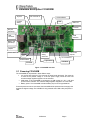
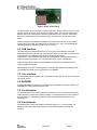
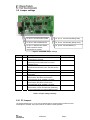
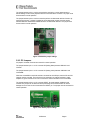
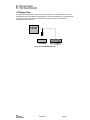
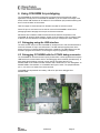
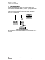
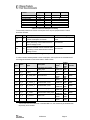
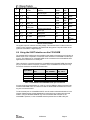
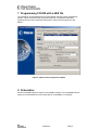
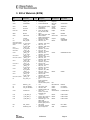
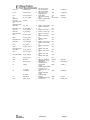
CC2430DB
Demonstration Board
User Manual
SWRU125
Page 1
Table of content
1
2
3
Introduction......................................................................................................................3
Definitions........................................................................................................................3
Kit content .......................................................................................................................3
3.1 Hardware.....................................................................................................................3
4
Getting started.................................................................................................................3
5
Hardware description CC2430DB....................................................................................4
5.1 Powering CC2430DB ..................................................................................................4
5.2 USB Interface..............................................................................................................5
5.3 User interface..............................................................................................................5
5.4 EEPROM.....................................................................................................................5
5.5 Accelerometer .............................................................................................................5
5.6 Potentiometer..............................................................................................................5
5.7 Light sensor.................................................................................................................6
5.8 I/O connectors.............................................................................................................6
5.9 Jumper settings...........................................................................................................7
5.9.1 P3 Jumpers ........................................................................................................7
5.9.2 P5 Jumpers ........................................................................................................8
5.10
Signal flow ..............................................................................................................9
6
Using CC2430DB for prototyping ..................................................................................10
6.1 Debugging using the USB interface ..........................................................................10
6.2 Debugging CC2430DB with the CC2430 debug connector .......................................10
6.3 Low power operation .................................................................................................11
6.4 Using the UART interface on the CC2430DB ............................................................13
7
Programming CC2430 with a HEX file...........................................................................14
8
Schematics....................................................................................................................14
9
Bill of Materials (BOM)...................................................................................................15
10 Document History ..........................................................................................................17
SWRU125
Page 2
1 Introduction
This manual contains reference information for the CC2430 DB hardware. The following tools,
which can be used with the kit, have their own user manual that can be downloaded from the
TI website:
- SmartRF® Studio
- Chipcon general packet sniffer
- IAR EW8051 C-compiler and C-Spy debugger (www.IAR.se)
The CC2430DB demonstration board includes a number of functions and applications that
allows quick testing of the RF interface and peripherals of the CC2430. It can for example be
used for:
•
•
•
Evaluation of SmartRF®04 products.
Measurement of current consumption. The kit is designed for low power operation,
and with an ampere meter the current consumption can be measured for all operating
modes.
Prototype development. The CC2430DB includes a USB interface that can be used
as emulator interface for the CC2430. Additionally, all I/O ports are available on pin
connector on the board to allow easy access for external applications.
2 Definitions
CC2430DB
USB MCU
Factory firmware
SoC
ICE
CC2430 Demonstration Board; described in this user manual
The Silicon Labs C8051F320 MCU used to provide a USB interface
on the CC2430DB
The firmware that is supplied programmed into the USB MCU from
the factory. This firmware supports SmartRF® Studio operation.
System on a Chip. A collective term used to refer to Chipcon ICs with
on-chip MCU and RF transceiver
In Circuit Emulator
3 Kit content
3.1 Hardware
The CC2430DB kit contains the following:
- 1 CC2430DB demonstration board
- 1 USB cable
- Quick start guide
- This document
4 Getting started
Make sure to install SmartRF® Studio before connecting the CC2430DB to a PC, as it installs
the required hardware drivers on the PC. SmartRF® Studio can be downloaded from the TI
web pages:
http://focus.ti.com/docs/toolsw/folders/print/smartrftm-studio.html
SWRU125
Page 3
5 Hardware description CC2430DB
Joystick
I/O connector A
CC2430 Reset
CC2430
debug
LED
Button S1
CC2430
DC jack
(Reverse)
USB
connector
PCB
Antenna
Battery clip
(Reverse)
Low current
jumpers
Power switch S3
USB MCU
debug
connector
Pot.
Low current
jumpers
I/O connector B
Accelerometer
Light sensor
EEPROM
USB MCU
Figure 1: CC2430DB overview
5.1 Powering CC2430DB
The CC2430DB can be powered in three different ways:
• 2.5 mm DC jack connector. This connector is placed under the board. The centre pin
is used for the positive voltage. A 4-10V DC power supply should be used. The
onboard voltage regulator supplies 3.3V to the board.
• USB power. If the CC2430DB is connected to a USB socket on a PC, it will draw
power from the USB bus. The onboard voltage regulator supplies 3.3V to the board.
• Battery power. The CC2430DB includes a battery clip for two AA type batteries
If several power sources are connected, the CC2430DB will be powered from the supply that
supplies the highest voltage. The USB MCU is only powered when USB or DC jack power is
used.
SWRU125
Page 4
Figure 2: Power switch setting
The Power Switch S3 must be set according to what power source is used. If DC jack or USB
power is applied, the switch should be set to the USB position. If the board is powered from
batteries, the switch should be set to the BATT position as shown in Figure 2. When either
DC power or batteries are used to power the board, the switch can be used as an on/off
switch.
When powering the CC2430DB from batteries, the CC2430 will work down to 1.8V. Please
note that when using USB, the voltage range is limited to 3.0V – 3.6V. The CC2430DB has
been designed for a temperature range of –40° C to +85° C.
5.2 USB Interface
The USB interface is used to interface to a PC to run the In-Circuit Emulator in the IAR
Embedded Workbench (IAR EW) and using SmartRF® Studio. The IAR EW can also be used
to reprogram the CC2430DB (see the IAR EW manual for more details).
Furthermore, it is also possible to reprogram the CC2430DB via the USB interface with the
Chipcon programming software, or to use the board for the Chipcon packet sniffer.
When connected to the USB port the CC2430DB is powered from the USB and no other
voltage supplies are required.
Please refer to the Chipcon Flash Programmer User Manual installed with SmartRF® Studio
for a detailed description of how to reprogram the CC2430DB.
5.3 User interface
The CC2430DB includes a joystick and a push button as user input devices, and two LEDs as
user output devices.
5.4 EEPROM
A 32Kbit EEPROM is included for non volatile storage of data that is frequently updated. The
EEPROM has 1 Million guaranteed write cycles.
5.5 Accelerometer
The accelerometer can be used to measure movements in 2 axes. It can also be used for tilt
measurements by measuring the earth’s gravitation. The accelerometer has a 20 ms start-up
time after power on. See the Analog Devices ADXL321 datasheet for details about the
accelerometer.
5.6 Potentiometer
The potentiometer controls the voltage on the analog input pin P0_7 of the CC2430. The
voltage, and thus the potentiometer position, can be measured with the CC2430 A/D
converter.
SWRU125
Page 5
5.7 Light sensor
A light dependent resistor (LDR) measures light level and gives an analog signal that is
measured by the CC2430 A/D converter. The light sensor resistance ranges from 5KΩ (light)
to 20MΩ (dark).
5.8 I/O connectors
The I/O connectors bring out all the signals from CC2430. These connectors allow easy
access to all CC2430 I/O pins. External circuitry can be connected to these connectors for
prototyping.
Pin
1
2
3
4
5
6
7
8
9
10
11
12
13
14
15
16
17
18
19
20
Function
VDD
VDD_SW_CONTROLLED1
P0_0/LDR
RESET_N
P0_1/BUTTON PUSH
P1_7/SO/MISO/UART_RD
P0_2/EE_SDA
P1_6/SI/MOSI/UART_TD
P0_3/EE_SCL
P1_5/SCLK/RTS
P2_1/DD
P1_4/CSN/SS/CTS
P2_2/DC
P2_0/JOY PUSH
P0_6/JOY
P1_2/VDD_SW_CTRL
P0_7/POT
P1_1/LED2
P1_0/LED1
GND
Table 1: I/O connector A (P6) pin-out
Pin
1
2
3
4
5
6
Function
P1_3/GPIO
DC_JACK_PWR
P0_4/ACC_X
VDD
P0_5/ACC_Y
GND
Table 2: I/O connector B (P7) pin-out
1
VDD_SW_CONTROLLED is controlled by the signal named VDD_SW_CTRL
SWRU125
Page 6
5.9 Jumper settings
P3, pin 5-6: Accelerometer self test
P5, pin 1-2: Connects DD (Debug Data)
P3, pin 3-4: SW controlled power
P5, pin 3-4: Connects DC (Debug Clock)
P3, pin 1-2: Replace with ampere
meter to measure current
consumption of CC2430
P5, pin 5-6: Connects RESET_N
Figure 3: CC2430DB Jumper settings
Header
P3
Pin
1-2
P3
3-4
P3
5-6
P4
P4
7-9
9-10
P5
1-2
P5
3-4
P5
5-6
Description
Replace with ampere meter to measure current
consumption of CC2430
SW controlled power. Can be removed when
performing current measurement to reduce
leakage current
Accelerometer self test. Mount to perform
accelerometer self test function. See also section
5.9.1.
Manual reset of USB MCU
Mount during power on to force USB MCU into
boot loader
Connects DD (Debug Data) between USB MCU
and CC2430. Should be removed when
connecting ICE to P8 “2430deb“ connector
Connects DC (Debug Clock) between USB MCU
and CC2430. Should be removed when
connecting ICE to P8 “2430deb” connector
Connects RESET_N signal between USB MCU
and CC2430. Can be removed when performing
current measurement to reduce leakage current
Default setting
Mounted
Mounted
Not mounted
Not mounted
Not mounted
Mounted
Mounted
Mounted
Table 3: Jumper settings summary
5.9.1 P3 Jumpers
The jumper between pin 1-2 on P3 can be replaced with an ampere meter to measure current
consumption of CC2430. The jumper must be mounted for normal operation.
SWRU125
Page 7
The jumper between pin 3-4 can be removed when performing current measurement to
reduce leakage current of the peripheral devices connected to the CC2430. The jumper must
be mounted for normal operation
The jumper between pin 5-6 can be mounted to perform accelerometer self test function. By
mounting this jumper, a voltage is applied to the accelerometer outputs. See the Analog
Devices ADXL321 datasheet for details about the accelerometer self test. The jumper must
be removed for normal operation.
Figure 4: Default P3 jumper settings
5.9.2 P5 Jumpers
All jumpers on header P5 must be mounted for normal operation.
The jumper between pin 1-2 on P5 connects DD (Debug Data) between USB MCU and
CC2430.
The jumper between pin 3-4 on P5 connects DC (Debug Clock) between USB MCU and
CC2430DB.
When the CC2430DB is used with emulator connected to the USB port, both the DD and DC
jumpers must be mounted. They should only be removed if an external emulator is used.
Chapter 6.2 gives instructions on how to connect the external emulator to the CC2430DB.
The jumper between pin 5-6 on P5 connects RESET_N signal between USB MCU and
CC2430. The jumper can be removed when performing current measurement to reduce
leakage current for the circuits connected to the RESET pin. The jumper must be mounted for
normal operation.
Figure 5: P5 default jumper settings
SWRU125
Page 8
5.10 Signal flow
The signal lines from the I/O connectors and the CC2430 run via 0Ω resistors to the various
peripherals on the CC2430DB. The peripherals can be disconnected from the CC2430 signal
pins by removing the 0Ω resistors. Please refer to Table 6 for a list of what resistors
correspond to which signals.
0 ohm
Figure 6: CC2430DB Signal flow
SWRU125
Page 9
6 Using CC2430DB for prototyping
The CC2430DB can be used for prototyping by programming the CC2430 with custom
applications. All I/O ports on the CC2430 are available on pin row header at the edge of the
board, and the USB interface can be used as In Circuit Emulator (ICE) interface allowing real
time in circuit emulation of the CC2430.
Table 6 on page 13 shows what pins on the MCU are used for various functions.
P6 and P7 pin-row connectors can be used to connect the CC2430DB to other PCB or
prototyping boards. See page 6 for the pin-out of these connectors.
0Ω resistors are included to isolate the CC2430 from the external components on the
CC2430DB. By removing these resistors, signals can be accessed on the pin headers. Refer
to section 5.10 and Table 6 for information about which pin corresponds to which resistor.
6.1 Debugging using the USB interface
The most common way to use the CC2430DB for development is to use the USB interface to
control the CC2430 on-chip In-Circuit Emulator. The USB interface supplies power to the
board, so there is no need for additional DC power or batteries. The USB interface can also
be used to program the CC2430 in circuit using the Chipcon programming software.
6.2 Debugging CC2430DB with the CC2430 debug connector
The CC2430DB can be used with the Chipcon packet sniffer or other applications that require
USB interface for communication with PC and debugging with an emulator simultaneously. In
these cases the SoC debug connector can be used for connecting the ICE. The
SmartRF04EB can be used as emulator interface with a cable from P14 “SoC debug/flash” on
SmartRF04EB to P8 “2430deb” on CC2430DB. See Figure 7 below. The jumpers between
pin 1-2, 3-4 and 4-5 on header P5 must be removed.
CC2430DB must be powered from battery, USB or DC jack when debugged from
SmartRF04EB.
Figure 7: CC2430 Debug Connector
SWRU125
Page 10
6.3 Low power operation
CC2430DB is designed for low power operation when running from batteries. Only the
CC2430 is powered in this mode, the USB MCU is not powered. The voltage to the peripheral
functions connected to the CC2430 is controlled by an I/O pin P1.2 (VDD_SW_CTRL) on the
CC2430. Table 4 lists the current consumption for each of the peripherals.
To obtain minimum current consumption with the CC2430DB, the VDD_SW_CTRL (P1.2)
output must be configured as output.
Figure 8: Voltage supply distribution
Table 4 below shows the current consumption for all modules and operation modes with 3.3V
supply voltage
SWRU125
Page 11
Active mode (mA)
Typical
Max
7,2
27
1
3
0,49
0,33
0,001
0.015
24
9mA
54mA
Device
CC2430
EEPROM
Accelerometer
Potentiometer
Light sensor
LEDs
Total
Power down mode (µA)
32KHz
Sleep
1µA
0.3µA
0
0
0
0
0
1µA
Table 4: Current consumption summary
To accurately measure the current consumption of the chip the jumpers listed in Table 5
should be removed.
Header
Pin
P3
1-2
P3
3-4
P5
5-6
Description
Replace with ampere meter to measure
current consumption of CC2430
SW controlled power. Can be removed
when performing current measurement to
reduce leakage current
Connects RESET_N signal between USB
MCU and CC2430. Can be removed when
performing current measurement to reduce
leakage current
Low power setting
Mounted, or connect ampere
meter
Not mounted
Not mounted
Table 5: Jumper setting for low power measurements
In order to achieve lowest possible current consumption, the I/O ports of the CC2430 should
be configured as listed in Power down state in Table 6 below.
2430
pin
Name
Schematic
Name
11
P0_0
P0_0/LDR
12
P0_1
P0_1/BUTTON
PUSH
Light dependent resistor
analog input
Push button interrupt active
low
13
P0_2
P0_2/EE_SDA
EEPROM SDA
14
P0_3
P0_3/EE_SCL
EEPROM SCL
15
P0_4
P0_4/ACC_X
Accelerometer x-axis
16
P0_5
P0_5/ACC_Y
Accelerometer y-axis
17
P0_6
P0_6/JOY
Joystick analog signal
18
P0_7
P0_7/POT
Potentiometer analog input
9
P1_0
P1_0/LED1
Green LED
8
P1_1
P1_1/LED2
Red LED
Description
Active
state2
IN
ANALOG
IN PULLUP
OUT
HIGH
OUT
HIGH
IN
ANALOG
IN
ANALOG
IN
ANALOG
IN
ANALOG
OUT
HIGH
OUT
HIGH
Power
down
state
OUT
LOW
0Ω ohm
resistor
R506
IN
OUT
LOW
OUT
LOW
OUT
LOW
OUT
LOW
OUT
LOW
OUT
LOW
OUT
HIGH
OUT
HIGH
2
R505
R504
R507
R508
R416
R430
Active state means that Software controlled VDD is on, this should only be enabled when
required by an I/O module
SWRU125
Page 12
6
P1_2
P1_2/VDD_SW
_CTRL
5
P1_3
P1_3/GPIO
4
P1_4
3
P1.5
2
P1_6
1
P1_7
48
P2_0
P2_0/Joy_push
46
P2_1
45
10
Voltage control for I/O
modules
Free I/O for controlling
external signal
OUT
HIGH
OUT
LOW
OUT
LOW
OUT
LOW
OUT
LOW
OUT
LOW
OUT
LOW
OUT
LOW
OUT
LOW
OUT
LOW
OUT
LOW
OUT
LOW
Joystick push interrupt
active high
IN
IN
P2_1/DD
Debug Data
IN
P2_2
P2_2/DC
Debug Clock
IN
RESET
RESET_N
Reset
P1_4/CSn/SS/
CTS
P1_5/SCLK/RT
S
P1_6/SI/MOSI/
UART_TD
P1_7/SO/MISO
/UART_RD
R305
R308
R306
R307
Jumper
P5
Jumper
P5
Jumper
P5
Table 6: Pinout CC2430
The joystick output is coded as an analog voltage. This has been done in order to save the
number of pins required on the MCU to interface with the joystick. The push function of the
joystick is connected to a digital input pin.
6.4 Using the UART interface on the CC2430DB
The CC2430 UART interface port is accessible on the header connectors as 3.3V signals. An
RS232 driver circuit is required to connect the UART interface on CC2430DB to a serial port
on a PC. The RS232 port on a SmartRF04EB can be connected to the CC2430DB to allow
applications to interface to a PC serial port.
Table 7 shows the connection between the CC2430DB and the SmartRF04EB. Both the P8
(10-pin) connector and the P6 (20-pin) connector on the CC2430DB can be used, but only
one of them should be connected at the same time.
Signal Name
RD
TD
RTS
CTS
GND
SmartRF04EB
P10
9
11
13
15
20
CC2430DB
P8, ”2430deb”
10
8
6
5
1
CC2430DB
P6, ”I/O A”
6
8
10
12
20
Table 7: CC2430ZDK to SmartRF04EB serial port connections
A jumper must be placed between pin 7 and pin 9 on the USB MCU debug connector P301
on the SmartRF04EB board. This will ensure that the Silabs USB controller does not force
any pins to erroneous levels.
To use the serial port on CC2430DB USART1 must be used on alternative location 2 in the
CC2430. Please see the CC2430 datasheet for instructions how to select serial port and
location. Using the SmartRF04EB will only work if the Silabs USB controller on the
CC2430DB is powered, i.e. the CC2430DB must be powered from a USB or DC jack.
SWRU125
Page 13
7 Programming CC2430 with a HEX file
The CC2430 can be programmed from the USB interface using the Chipcon programming
software. Figure 9 shows the flash programming interface. For additional information
regarding Chipcon Flash Programmer please refer to Chipcon Flash Programmer User
Manual.
Figure 9: Chipcon Flash programmer software
8 Schematics
See the CC2430DB Reference Design for CC2430DB schematics. The CC2430DB reference
design can be downloaded from the product page for CC2430DB on TI’s websites.
SWRU125
Page 14
9 Bill of Materials (BOM)
Ref.
Part name
Pcs/
unit
B1-2
1XAA_1_5V
2
Description
Mounting clip for one
AA battery cell
U500
24AA32A/SN
1
4 KB I2C EEPROM
U401
AD8544
1
Rail-to-rail quad opamp
18 g peak X,Y
accelerometer
U501
ADXL321
1
D100-101
BAT254
2
Q300
BC846
1
U300
C8051F320
1
U1
CC2430
C_1U_0402_
X5R_K_6P3
1
C71
C207;C281;C300;
C400;C471;C500;
C503
1
Diode, Si, Schottkey
BJT, Si, NPN, smallsignal
Silicon Labs 8051 USB
Microcontroller
Single-chip transceiver
and microcontroller
Capacitor 1uF, 0402,
X5R,10%, 6.3V
Manufacturer
Part number
Keystone
Microchip
Analog
Devices
Analog
Devices
24AA32A/SN
Philips
BAT254
Philips
BC846B
Silicon Labs
C8051F320
Chipcon
Murata
CC2430
GRM155R60
J105KE19D
murata
GRM21BR61A106K
Murata
GRM21
AD8544AR
ADXL321
C251;C271;C381
C_100N_0402
_X5R_K_10
C_100P_0402
_NP0_J_50
C_10N_0402
_X7R_K_25
C_10U_0805
_X5R_L_25
C_15P_0402
_NP0_J_50
C_220N_0402
_X5R_K_10
C_220N_0603
_X7R_K_50
C_33P_0402
_NP0_J_50
C_2U2_0603
_X5R_K_10
C_33N_0402
_X7R_K_25
C_4U7_0805
_X5R_K_6
C_5P6_0402
_NP0_J_50
C_68P_0402
_NP0_J_50
P2
DC_JACK_2.5
1
U101
EM6353_1_8V
1
Capacitor, 100n, 0402,
X5R, 10%, 10V
Capacitor, 100p, 0402,
NP0, 5% 50V
Capacitor, 10n, 0402,
X7R, 10%, 25V
Capacitor, 10u, 0805,
XR5, 15% 25V
Capacitor, 15p, 0402,
NP0, 5%, 50V
Capacitor, 220n, 0402,
X5R, 10%, 10V
Capacitor, 220n, 0603,
X7R, 10%, 50V
Capacitor, 33p, 0402,
NP0, 5%, 50V
Capacitor, 2u2, 0603,
X5R, 10%, 10V
Capacitor, 33n, 0402,
X7R, 10%, 25V
Capacitor, 4U7, 0802,
X5R, 10%, 6.3V
Capacitor, 5p6, 0402,
NP0, 5%, 50V
Capacitor, 68p, 0402,
NP0, 5% 50V
DC jack, 2.5mm center
pin
brown-out detector,
200ms delay,
SOT23-3 "beta" pinout,
1.8V
D1
LED_CL150GCD
1
LED, green, 1206
Citizen
CL150GCD
D2
LED_CL150URCD
1
LP2985-3.3V
1
Citizen
National
Semiconductor
CL150URCD
U100
LED, red, 1206
Voltage regulator, low
noise, 3.3 V
Inductor, 1n8, 0402,
Monolithic type,
+/-0.3 nH
Murata
LQG15-series
Inductor, 22n, 0402, 5%
Inductor, 6n8, 0402,
Monolithic type, +/-5%
Silonix CdS
photoconductive cell
5 kOhm (light) to 20 M
Ohm (dark)
2x10 pinrow, 2.54mm
pitch, through-hole
Murata
LQG15-series
Murata
LQG15-series
Silonix
NSL-19M51
AMP
5-0826632-0
C401
C101;C351;
C501-502
C102
C431;C441
C231;C411;C421
C241
C191;C211
C103
C104
C100
C341
7
1
4
1
2
3
1
2
1
1
1
1
3
L341
L_1N8_0402_S
1
L331
L_22N_0402_J
1
L321
L_6N8_0402_J
1
RP1
NSL_19M51
1
P6
PINROW_2X10
1
SWRU125
EM
Microelectronic
EM6353
LP2985AIM5-3.3
Page 15
P3;P5;P7
PINROW_2X3
3
P4;P8
PINROW_2X5
2
S1-2
PUSH_BUTTON
2
RT1
R303-304;
R311-312
R100;R305;R306307;
R308;R416;R430;
R504-508
R_0-10K_TRIM
1
R_0603
4
R_0_0603
12
2x3 pinrow, 2.54mm
pitch, through-hole
2x5 pinrow, 2.54mm
pitch, through-hole
Momentary pushbutton, SMD
10k trimming pot with
knob
Resistor, general, 0603;
Do not mount
AMP
0-0826632-3
AMP
0-0826632-5
Alps
BI
Technologies
SKHUAF
72PTR10K
R405;R410-412
R_100K_0402_F
4
Resistor, 0 ohms, 0603
Resistor, 100k, 0402,
1%
R413-415
R_10K_0402_F
3
Resistor, 10k, 0402, 1%
Koa
R300-302
R403-404;R407;
R501
R_1K0_0402_J
3
Koa
R_200K_0402_F
4
R409
R_220K_0402_F
1
Resistor, 1k, 0402, 5%
Resistor, 200k, 0402,
1%
Resistor, 220k, 0402,
1%
Resistor, 270 ohm,
0402, 1%
Resistor, 2k2, 0402, 2%
Resistor, 2 ohm, 0402,
1%
Resistor, 330k, 0402,
1%
Resistor, 43K, 0402,
1%
Resistor, 470k, 0402,
1%
Resistor, 4.7k, 0402,
2%
Resistor, 56K, 0402,
1%
Koa
MOS-FET, p-channel
Double switch, ALPS
SSSS222700
USB B-style PCBmount socket
Crystal,
32.000MHz,NX3225DA,
10/15ppm, 16 pF !
Temp range -30 - +85
deg C !
Crystal, 32.768 kHz,
12.5pF,
20/50 ppm,SMD
package
4-directional switch with
a centre push
Siliconix
SI9424DY
ALPS
SSSS222700
AMP
787780-1
NDK
NX3225DA
Epson
MC-306
Alps
skrhab_e010
R400;R440-441
R_270_0402_F
3
R502-503
R_2K2_0402_G
2
R241
R_2_0402_F
1
R406
R101;R261;R310;
R401;R420
R_330K_0402_F
1
R_43K_0402_F
5
R402
R_470K_0402_F
1
R102;R309;R509
R_4K7_0402_G
3
R221
R_56K_0402_F
1
Q100
SI9424DY
1
S3
SWITCH_6PIN
1
P1
USB_B
1
X1
X_32.000/
10/15/30/16
1
X2
X_32.768/
20/50/40/12
1
U400
skrhab_e010
1
SWRU125
Koa
Koa
Koa
Koa
Koa
Koa
Koa
Koa
Koa
Koa
Koa
Page 16
10 Document History
Revision
1.0
Date
2007-04-16 Initial release
SWRU125
Description/Changes
Page 17
IMPORTANT NOTICE
Texas Instruments Incorporated and its subsidiaries (TI) reserve the right to make corrections, modifications, enhancements,
improvements, and other changes to its products and services at any time and to discontinue any product or service without notice.
Customers should obtain the latest relevant information before placing orders and should verify that such information is current and
complete. All products are sold subject to TI’s terms and conditions of sale supplied at the time of order acknowledgment.
TI warrants performance of its hardware products to the specifications applicable at the time of sale in accordance with TI’s
standard warranty. Testing and other quality control techniques are used to the extent TI deems necessary to support this
warranty. Except where mandated by government requirements, testing of all parameters of each product is not necessarily
performed.
TI assumes no liability for applications assistance or customer product design. Customers are responsible for their products and
applications using TI components. To minimize the risks associated with customer products and applications, customers should
provide adequate design and operating safeguards.
TI does not warrant or represent that any license, either express or implied, is granted under any TI patent right, copyright, mask
work right, or other TI intellectual property right relating to any combination, machine, or process in which TI products or services
are used. Information published by TI regarding third-party products or services does not constitute a license from TI to use such
products or services or a warranty or endorsement thereof. Use of such information may require a license from a third party under
the patents or other intellectual property of the third party, or a license from TI under the patents or other intellectual property of TI.
Reproduction of information in TI data books or data sheets is permissible only if reproduction is without alteration and is
accompanied by all associated warranties, conditions, limitations, and notices. Reproduction of this information with alteration is an
unfair and deceptive business practice. TI is not responsible or liable for such altered documentation.
Resale of TI products or services with statements different from or beyond the parameters stated by TI for that product or service
voids all express and any implied warranties for the associated TI product or service and is an unfair and deceptive business
practice. TI is not responsible or liable for any such statements.
TI products are not authorized for use in safety-critical applications (such as life support) where a failure of the TI product would
reasonably be expected to cause severe personal injury or death, unless officers of the parties have executed an agreement
specifically governing such use. Buyers represent that they have all necessary expertise in the safety and regulatory ramifications
of their applications, and acknowledge and agree that they are solely responsible for all legal, regulatory and safety-related
requirements concerning their products and any use of TI products in such safety-critical applications, notwithstanding any
applications-related information or support that may be provided by TI. Further, Buyers must fully indemnify TI and its
representatives against any damages arising out of the use of TI products in such safety-critical applications.
TI products are neither designed nor intended for use in military/aerospace applications or environments unless the TI products are
specifically designated by TI as military-grade or "enhanced plastic." Only products designated by TI as military-grade meet military
specifications. Buyers acknowledge and agree that any such use of TI products which TI has not designated as military-grade is
solely at the Buyer's risk, and that they are solely responsible for compliance with all legal and regulatory requirements in
connection with such use.
TI products are neither designed nor intended for use in automotive applications or environments unless the specific TI products
are designated by TI as compliant with ISO/TS 16949 requirements. Buyers acknowledge and agree that, if they use any
non-designated products in automotive applications, TI will not be responsible for any failure to meet such requirements.
Following are URLs where you can obtain information on other Texas Instruments products and application solutions:
Products
Applications
Amplifiers
amplifier.ti.com
Audio
www.ti.com/audio
Data Converters
dataconverter.ti.com
Automotive
www.ti.com/automotive
DSP
dsp.ti.com
Broadband
www.ti.com/broadband
Interface
interface.ti.com
Digital Control
www.ti.com/digitalcontrol
Logic
logic.ti.com
Military
www.ti.com/military
Power Mgmt
power.ti.com
Optical Networking
www.ti.com/opticalnetwork
Microcontrollers
microcontroller.ti.com
Security
www.ti.com/security
Low Power
Wireless
www.ti.com/lpw
Telephony
www.ti.com/telephony
Video & Imaging
www.ti.com/video
Wireless
www.ti.com/wireless
Mailing Address: Texas Instruments, Post Office Box 655303, Dallas, Texas 75265
Copyright © 2007, Texas Instruments Incorporated