1
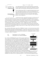
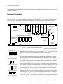
address $2000, and are allocated $300 words per program. They are read into the internal DSP memory spaces
P:APL_ADR to $1FF, X:COM_TBL to COM_TBL+15, and Y:0000 to Y:$00FF. The EEPROM memory map
is shown in Fig. 4-4, and the source code files "utilboot.asm" and "utilappl.asm" can be referred to for further
clarification. Currently an application program for testing the utility board is supplied, contained in the file
"utiltest.asm", and is assigned application number 1.
Application number zero is a special case and is designated for large application programs that cannot execute
in their entirety from internal DSP P: memory space. Instructions located at EEPROM address P:$200 up to
P:$1EE0) will be executed directly from EEPROM. Instructions from P:APL_ADR to P:$1FF will be read from
EEPROM into DSP P: memory by the ’LDA 0’ command. Its EEPROM memory map is also shown in Fig 4-4.
The PAL U31 has been designed into the current hardware revision 3B to generate DSP reset and interrupts
more reliably than earlier versions. The PAL has been programmed to reset the DSP to operating mode 2
wherein the DSP begins execution from EEPROM address $C000 after reset rather than reading the program
from byte-wide memory into DSP and then executing it, as is done in operating mode 1. Earlier revisions of the
DSP software than Rev. 2.25 can be executed on the current hardware revision 3B, but a different PAL will
need to be generated to reset the DSP to operating mode 1 instead.
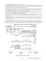
The jumper JP11 is installed in the default configuration as shown in Fig. 4-2 to enable the watchdog timer. It
contains a timer circuit that will reset the DSP unless the watchdog timer is itself reset more often than that. The
intention is to require the DSP to reset the watchdog timer more often than every 10 milliseconds as a sign that
it is properly functioning; otherwise the DSP will be reset. The timer circuit is reset with a simple read instruction from location $FFF7.
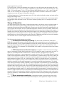
The two jumpers JP7 and JP8 supply power to the board from either the backplane or the CCD/User connector.
The default is to supply +/- 15 volt power from the backplane to the utility board. Some users may desire to
supply it through the CCD/User connector instead so the utility board can independently verify the integrity of
the backplane power supply before turning it on and powering up the CCDs. In that case the two jumpers on
JP7-8 should be moved to the 2-3 position, the separate power should be run to the CCD/User connector
through pins C01 (+15 V) and A01 (-15 V), and a sample of the backplane power before it is supplied to the
backplane should be run to several of the inputs AIN8-15 after being suitably divided so they are in the range
of +3 to -3 volts that the A/D requires. Note that the spacing of the pins of JP7-8 are larger than 0.10 inches so
standard jumpers cannot be installed - the intention of having soldered wires is to discourage accidental
re-configurations.
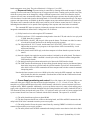
The utility board needs to be installed in either slot 1 or slot 6 of the VME system backplane if a power control
board is being used. Alternatively, the daisy-chained lines A21, A22 and B04 need to have jumpers attached to
them on the VMEbus backplane to connect them between the utility board and the power control board.
Board Checkout
The following procedure is followed in verifying operation of the board. The commands to be executed are
described later in this chapter.
(1) Visually inspect board: The correct ROM(s) should be installed; if there is only one ROM it should be in
the left-most socket. Check the DSP. The jumpers described above should be installed correctly, as should all
the resistors.
(2) Power supplies: The +5 should be available at the logic devices, and +/- 12 volts should be available at the
regulators and the analog components. With the power control board installed, and the utility board installed in
either slot 1 or 6, PON will turn on the analog voltages. If it doesn’t install jumpers on the power control lines
4-3
Utility board - Updated May 12, 1994