1
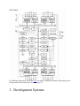
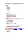
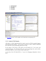
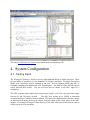
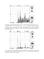
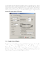
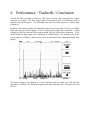
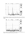
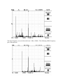
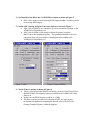
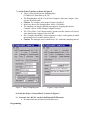
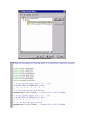
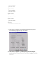
Narrow Band Filter Implementation On A Low Cost Microcontroller Issues and Performance ©2001 Erick L. Oberstar Michael J. Bauch Table of Contents 1. Project Summary 2. Atmel AVR Summary 3. Development Systems 3.1. Hardware – Atmel STK500 Starter Kit 3.2. Software Development Systems 3.2.1. CodeVision AVR C Compiler 3.2.2. Atmel AVR Studio Assembler/Debugger 4. System Configuration 4.1. Analog Input 4.2. Analog Output 4.3. Sampling Rate 5. DSP 5.1. 5.2. 5.3. Filter Design Fixed Point Representation Fixed Point Effects 6. Performance / Tradeoffs / Conclusion 7. Appendix 7.1. C Souce File 7.2. Matlab Souce Files 7.3. DSP on an AVR - Lab Procedure 7.4. Referenced Materials 1. Project Summary The purpose of this project was to investigate the issues relating to the implementation of a digital filter on a low cost microcontroller platform rather than an expensive and special purpose Digital Signal Processor (DSP) system. In particular a 1KHz center frequency, 500 Hz bandwidth narrow band filter was implemented. Issues relating to sampling rate, fixed point mathematics, and signal reconstruction were observed and investigated. Overall system performance was also observed. 2. Atmel AVR Summary Atmel's AVR microcontrollers have a RISC core running single cycle instructions and a welldefined I/O structure that limits the need for external components. Internal oscillators, timers, UART, SPI, pull-up resistors, pulse width modulation, ADC, analog comparator and watch dog timers are some of the features in AVR devices. AVR instructions are tuned to decrease the size of the program whether the code is written in C or Assembly. With on-chip in-system programmable Flash and EEPROM, the AVR is a reasonable choice to optimize for cost and get products to market quickly. The part selected to implement a simple 2nd order digital filter is the ATmega163. The ATmega163 belongs to the Atmel AVR family of 8-bit RISC microcontrollers. This part runs up to 8MHz, and has 16KB of FLASH (Program) memory, 512 byte of EEPROM (Nonvolatile Data Memory), 1KB of SRAM, 32 I/O lines, 17 hardware interrupts, 3 counter timers, an 8 channel 10-bit A/D, and various other on chip peripheral modules. Key features used by the filter project were: one counter timer for interrupt service routine timing; A/D converter for sampling an analog waveform; one counter timer for Pulse Width Modulation (PWM) timing for an inexpensive analog output; a hardware integer multiply; and a “C friendly” instruction set. Additional features from the Atmel Datasheet are: Features • High-performance, Low-power AVR ® 8-bit Microcontroller – 130 Powerful Instructions - Most Single Clock Cycle Execution – 32 x 8 General Purpose Working Registers – Fully Static Operation – Up to 8 MIPS Throughput at 8 MHz – On-chip 2-cycle Multiplier • Nonvolatile Program and Data Memories • Self-programming In-System Programmable Flash Memory – 16K Bytes with Optional Boot Block (256 - 2K Bytes) Endurance: 1,000 Write/Erase Cycles – Boot Section Allows Reprogramming of Program Code without External Programmer – Optional Boot Code Section with Independent Lock Bits – 512 Bytes EEPROM Endurance: 100,000 Write/Erase Cycles – 1024 Bytes Internal SRAM – Programming Lock for Software Security • Peripheral Features – Two 8-bit Timer/Counters with Separate Prescaler and Compare Mode – One 16-bit Timer/Counter with Separate Prescaler, Compare Mode, and Capture Mode – Real Time Clock with Separate Oscillator and Counter Mode – Three PWM Channels – 8-channel, 10-bit ADC – Byte-oriented 2-wire Serial Interface – Programmable Serial UART – Master/Slave SPI Serial Interface – Programmable Watchdog Timer with Separate On-chip Oscillator – Analog Comparator • Special Microcontroller Features – Power-on Reset and Programmable Brown-out Detection – Internal Calibrated RC Oscillator – External and Internal Interrupt Sources – Four Sleep Modes: Idle, ADC Noise Reduction, Power Save, and Power-Down • Power Consumption at 4 MHz, 3.0V, 25ο...C – Active 5.0 mA – Idle Mode 1.9 mA – Power-down Mode < 1 µA • I/O and Packages – 32 Programmable I/O Lines – 40-pin PDIP and 44-pin TQFP • Operating Voltages – 2.7 - 5.5V (ATmega163L) – 4.0 - 5.5V (ATmega163) • Speed Grades – 0 - 4 MHz (ATmega163L) – 0 - 8 MHz (ATmega163) The datasheet for the ATmega163 is included with this cd. Further feature specifications are available by following this link to the Atmel datasheet. The processor block diagram follows below: For additional information follow this link to an Atmel Corporation internal AVR training Power Point presentation located on the accompanying CD. 3. Development Systems 3.1 Hardware - Atmel STK500 Starter Kit The Atmel STK500 is a complete starter kit and development system for the AVR Flash microcontroller from Atmel Corporation. It is manufactured and sold by Atmel for the purposes of part evaluation and prototype development. The entire STK500 users guide can be found on this cd by following this link. The features for the STK500 listed below are from the AVR STK500 User Manual. Features • AVR Studio ® Compatible • RS232 Interface to PC for Programming and Control • Regulated Power Supply for 10 - 15V DC Power • Sockets for 8-pin, 20-pin, 28-pin and 40-pin AVR Devices • Parallel and Serial High-voltage Programming of AVR Parts • Serial In-System Programming (ISP) of AVR Parts • In-System Programmer for Programming AVR Parts in External Target System • Reprogramming of AVR Parts • 8 Push Buttons for General Use • 8 LEDs for General Use • All AVR I/O Ports Easily Accessible through Pin Header Connectors • Additional RS232 Port for General Use • Expansion Connectors for Plug-in Modules and Prototyping Area • On-board 2-Mbit DataFlash ® for Nonvolatile Data Storage AVR Studio, version 3.2 or newer, supports the STK500. For up-to-date information on this and other AVR tool products, please read the document “avrtools.pdf” (AVR Studio Users Guide). The newest version of AVR Studio, “avrtools.pdf”, and the user guide can be found in the AVR section of the Atmel Web site. 3.2 Software Development System Software was developed using a pair of applications. Application source code was developed using a third party C compiler called CodeVisionAVR (CVAVR). Source code debugging was performed using Atmel’s Integrated Development Environment (IDE) called AVR Studio. The hardware platform was programmed from the CVAVR compiler IDE using the AVR Studio programmer. 3.2.1 CodeVisionAVR (CVAVR) C Compiler CodeVisionAVR is a third party C compiler targeted at the Atmel AVR line of RISC microcontrollers. It is build by HP InfoTech, a Romanian one-man company. CVAVR is used for source code development. A list of CVAVR features copied from the HP InfoTech website (http://infotech.ir.ro/) is included below: Features • • • • • • • • 32 bit application, runs under Windows 95, 98, NT 4.0 and 2000 Easy to use Integrated Development Environment and C Compiler Editor with auto indentation and keywords highlighting Supported data types: bit, char, int, short, long, float, double AVR specific extensions for: Accessing the EEPROM & FLASH memory areas Bit level access to I/O registers Interrupt support Compiler optimizations: Peep-hole optimizer Advanced variables to register allocator, allows very efficient use of the AVR architecture Common Block Soubroutine Packing, replaces repetitive code sequences with calls to subroutines Loop optimization Branch optimization Subroutine call optimization Cross-jumping optimization Constant folding Store-copy optimization Dead code removing optimization Two memory models: TINY (8 bit data pointers for chips with up to 256 bytes of RAM) and SMALL (16 bit data pointers for chips with more than 256 bytes of RAM) for better code efficiency User selectable optimization for Size or Speed Possibility to insert assembler code directly in the C source file VERY EFFICIENT USE OF RAM: Constant character strings are stored only in FLASH memory and aren't copied to RAM, like in other compilers for the AVR • • • • • • • C Source level debugging, with COFF symbol file generation, allows variable watching and the use of the Terminal I/O in Atmel’s AVR Studio 3.22 Debugger Fully compatible with Atmel’s In-Circuit Emulators Supported chips: ATtiny22 AT90S2313 AT90S2323/2343 AT90S2333/4433 AT90S4414/8515 AT90S4434/8535 AT90S8534 ATmega603/103 ATmega161 ATmega163 ATmega32A FPSLIC AT94K10/20/40 Supplementary libraries for: Alphanumeric LCD modules for up to 4x40 characters Philips I²C Bus National Semiconductor LM75 Temperature Sensor Dallas DS1621 Thermometer/Thermostat Philips PCF8563 and PCF8583 Real Time Clocks Dallas DS1302 and DS1307 Real Time Clocks Dallas 1 Wire protocol Dallas DS1820/DS1822 Temperature Sensors SPI Power management Delays Built-in CodeWizardAVR Automatic Program Generator, allows you to write in a matter of minutes all the code needed for implementing the following functions: External memory access setup Chip reset source identification Input/Output Port initialization External Interrupts initialization Timers/Counters initialization Watchdog Timer initialization UART initialization and interrupt driven buffered serial communication with the following parameters: 7N2, 7E1, 7O1, 8N1, 8N2, 8E1 and 8O1 Analog Comparator initialization ADC initialization SPI Interface initialization I²C Bus, LM75 Temperature Sensor, DS1621 Thermometer/Thermostat, PCF8563, PCF8583, DS1302 and DS1307 Real Time Clocks initialization 1 Wire Bus and DS1820/DS1822 Temperature Sensors initialization LCD module initialization Built-in Serial Communication Terminal for debugging RS232, RS422, RS485 Built-in In-System AVR Chip Programmer, compatible with the Atmel STK500, Kanda Systems STK200 and STK300 development boards, Vogel Elektronic VTEC-ISP, Dontronics DT006, with automatic programming after successful compilation. Supported chips: AT90S1200 ATtiny12/15L/22 AT90S2313 AT90S2323/2343 AT90S2333/4433 AT90S4414/8515 AT90S4434/8535 ATmega603/103 ATmega161 ATmega163 ATmega32A A screen grab of the compiler is shown below: The full manual for the CVAVR compiler can be found on the accompanying CD. 3.2.2 Atmel AVR Studio AVR Studio is a Win32 application built by Atmel to provide an IDE for assembly language code generation and simulation. It also provides an interface to Atmel’s STK500 AVRFlash MCU Starter Kit for part programming and hardware testing. For the purpose of this project, AVR Studio was used primarily for C level source code simulation/debugging. The AVR Studio IDE can be used to step through code, watch variables, and stimulate registers as well as I/O pins in both assembly and C. A screen shot of the AVR Studio IDE in a C source level debugging configuration is shown below: The entire AVR Studio User Guide can be found on the accompanying CD. 4. System Configuration 4.1 Analog Input The ATmega163 features a 10-bit successive approximation analog to digital converter. There are two modes of operation: (1) Free Running (2) Single Conversion. In Single Converstion Mode, each conversion must be initiated by the user. In Free Running Mode, the ADC is constantly sampling and updating the ADC Data Register. The fifth bit of the ADCSR register selects between these modes. Any pin of PortA may be chosen as the ADC input via a multiplexer. The ADC supports single ended conversion between 0 and 5 volts. The conversion time ranges between 65 and 260 micro seconds. . The ADC may operate up to 15kSPS at maximum resolution and up to 76kSPS at 8-bit resolution. The successive approximation circuitry requires an input clock frequency that may be chosen from pre-scaled system clock values in the ADC module. According to ATmega163 Data Sheet p.98, the ADC clock must be less than or equal to 1MHz to provide 8 bit resolution. A worse case conversion rate is 25 ADC clock cycles. The conversion time must obviously be shorter than the sampling interval to produce relevant digital values. So 25 times the ADC clock period must be less than the sampling period or equivalently, the ADC clock frequency must be 25 times greater than the sampling rate. For a 12.048 kHz sampling rate, the ADC clock frequency must be greater than approximately .3012 MHz. An ADC clock frequency of 1MHz satisfies the upper boundary of the preceding paragraph and the lower boundary just mentioned. 4.2 Analog Output - Pulse Width Modulation A common and inexpensive D/A converter can be implemented using a PWM digital output and a simple/inexpensive analog filter. A full application-note (AN538 - written by Microchip Technology) describing PWM and the key issues regarding it is found on the accompanying CD . The principle concept of PWM is to vary the duty cycle of a square wave at some fundamental frequency. This PWM square wave is then low pass filtered at a corner frequency much less than the fundamental frequency of the square wave to pass output signals up to the corner frequency. For the Atmel ATmega163, Timer 1 was configured for PWM generation. Timer 1 on the Atmega163 is a 16-bit counter timer that can count at full system clock speed, a prescaled value of the system clock, or an external input clock. When configured in PWM mode, Timer 1 has two compare registers that provide 8, 9, or 10 bit resolution on the PWM output duty cycle. Timer 1 in PWM mode can be configured to have two independent PWM outputs. The duty cycle of each output is set by writing the 8, 9, or 10 least significant bits (depending on resolution) to the corresponding duty cycle register. For more detailed information on the counter timer one see page 36 in the ATmega163 datasheet included on the accompanying CD. For this application, Timer 1 was configured for PWM output in an 8-bit mode with frequency doubling enabled. Given the system oscillator frequency f TCK 1 the PWM output frequency in 8bit mode with frequency doubling is given by the equation: f 8MHz f PWM = TCK 1 = = 31.25KHz 256 256 This PWM mode was selected to make the PWM fundamental frequency as high as possible. This maximizes the possible bandwidth of the digitally filtered output signal. The PWM output signal was filtered using two sequential single pole RC filters. Both filters were designed for the same -3dB frequency to provide a second order filter. The RC filter corner frequency is given by the equation: 1 f -3dB = 2πRC A corner frequency of 2.5 KHz was desired. A resistor value of 150Ω and capacitor value of 0.47 µF were chosen giving f -3dB = 2.26 KHz . The spectrum of the unfiltered PWM signal (with no digital filter input signal) is shown below. This plot shows the PWM fundamental frequency at 31.25 KHz and the first harmonic at 2 f PWM . The PWM output is low pass filtered at f ALPF << f PWM to attenuate the high frequency contributions from the raw square wave signal while passing lower frequency components obtained by the pulse width modulation. The low pass filtered PWM signal without digital filter input is shown below. It is worth noting that the PWM output filter attenuates the fundamental ~22dB which corresponds to the expected attenuation because the plot is a power spectrum measurement rather than a voltage or current spectrum. 4.3 Sampling Rate The system utilized one of the counter timers with interrupt support on the Atmega163 for deterministic input signal sampling, input signal filtering, and output signal updating. Counter Timer 2 was configured to use the full 8 MHz system clock in an output compare mode with the output disconnected. The timer was configured to clear itself and generate an interrupt on a compare match. The Timer 2 compare register was loaded with a hex value that results in a 12.048 KHz interrupt rate with an 8 MHz system clock. 5. DSP 5.1 Filter Design In order to build a narrow-band digital filter, start with a simple second order continuous-time band pass filter: H (s) = sG ( s − s0)( s − s0*) As a narrow-band approximation (B<<f0) place the poles as shown below: s 0 = −πB + j 2πf 0 s 0 = −πB − j 2πf 0 where: B = Desired Band Width (based on 3dB attenuation) f0 =Desired Center frequency G = scale factor to control over all filter gain H ( s) = sG s 2 − s ( s 0 + s 0*) + s 0 s 0 * s0 + s0* = −2πB s 0 * s 0* = π 2 B 2 + 4π 2 f 0 2 Let p = Let q = H (s) = sG s 2 − ps + q Next apply the bilinear transform: 2 (1 − z −1 ) s= T (1 + z −1 ) T = sampling interval 2G 2G − z −2 4 2p 4 2p + + + + q) ( ) ( T q T −1 2 2 2 (1− z ) T T T T = H −1 8 4 2p T (1+ z ) − +q 2q − 2 2 −1 T T T z −2 1+ z + 4 2p 4 2p ( 2 + + q) ( 2 + + q) T T T T Equate the coefficients with the general second order digital infinite impulse response filter: b0 + b1z −1 + b2 z −2 H ( z) = 1 + a1z −1 + a 2 z −2 b0 = 8 T2 a1 = 4 2p + q) ( 2+ T T 2q − 2G 4 2p + q) T( 2 + T T b1 = 0 b2 = − 2G 4 2p T( 2 + + q) T T 4 2p − +q 2 T T a2 = 4 2p ( 2+ + q) T T Prewarping: 2 (1 − z −1 ) s= T (1 + z −1 ) The bilinear transform does not produce a perfectly linear relationship between analog and digital frequencies especially for higher frequencies: 2 (1 − e − jωd ) jω a = T (1 + e − jωd ) , s = jωa z = e jωd tan(πfdT ) fa = πT Therefore, in order to design for a center frequency (fd) and bandwidth (fd_max-fd_min) similar to that of the analog filter, the digital filter coefficients must be calculated with f0 = fa and B=Ba = fa_max – fa_min. Unity gain desired at center frequency: H ( j 2πfa ) = 2πfaG πBa π 2 Ba 2 + 16π 2 fa 2 Ba π 2 Ba 2 + 16π 2 fa 2 G= 2 fa Difference Equation: y[n ] = −a1 y[n − 1] − a 2 y[n − 2] + b0 x[n ] + b1x[n − 1] = b2 x[n − 2] 5.2 Fixed Point Representation To more accurately construct the digital filter, floating point data and coefficient values should be used. However there is significant processor overhead required to perform floating point calculations. Floating point overhead limits the effective sampling rate of the filter because interrupt service routine (ISR) takes extra time to execute thus lowering the highest possible ISR execution rate. To improve mathematical throughput and increase the ISR execution rate (i.e. increase sampling rate) calculations are performed using two’s complement signed fixed point representations. Q7 and Q6 8-bit fixed point representations for input samples and filter coefficients respectively, were chosen because the low cost microcontroller selected is natively 8-bit. Q7 numbers can represent fixed-point numbers ranging from –1 to 0.9921875 in increments 0.0078125 (-1 to 1 1/128). The 8-bit Q7 number bit weighting is shown below. The decimal place is between bits 6 and 7. Input samples are in a Q7 format. |s . | x | x | x | x | x | x | x | -1 | 1/2 | 1/4 | 1/8 | 1/16 | 1/32 | 1/64 | 1/128 Eight bit Q6 numbers can represent fixed point numbers ranging from –2 to 1.984375 in increments 0.015625 (-2 to 2 - 1/64). The Q6 representation bit weighting is shown below. The decimal place is between bits 5 and 6. Filter coefficients are in a Q6 format. | s | x. | x | x | x | x | x | x | -2 | 1 | 1/2 | 1/4 | 1/8 | 1/16 | 1/32 | 1/64 When a Q7 and Q6 number are multiplied (both 8 bit numbers) the result is a 16-bit Q13 number. Q13 numbers range from –4 to 3.9998779296875 in increments of 0.0001220703125 (4 to 4 – 1/8192). The Q13 representation bit weighting is shown below. | s | x | x. | x | x | x | x | x | x | x | x | x | x | x | x | x | | -4 | 2 | 1. | 1/2 | 1/4 | x | x | x | x | x | x | x | x | x | x | 1/8192 | The 16-bit Q13 number is scaled back to a Q7 representation for the digital filter’s output. This Q7 number is contained in the bit just left of the decimal place and the seven bits just below the decimal place. These Q7 bits are extracted by shifting the 16-bit Q13 number right six bits and selecting only the low byte of the 16-bit value. The resulting 8-bit Q7 number is shown below. 8-bit Q7 A critical detail is that the 8-bit Q7 & Q6 numbers must be a signed data type in C. This is important because when a product of a Q7 & Q6 number is calculated the 8-bit values must be sign extended to 16-bits to do the multiplication correctly. A point of caution: The CodeVision compiler contains switches to make “char” data types unsigned by default as well as to allow automatic promotion of “char” types to “int”. See the below project configuration block showing these switches and the correct settings. 5.3 Fixed Point Effects Fixed point representation effects several areas of the filter design/response. Since the filter coefficients are represented by 8-bit Q7 and Q6 fixed point format, the coefficients can only have quantum values. The worst case 8-bit Q7 coefficients can be off by ±1/256. The worst case 8bit Q6 coefficients can be off by ±1/128. As the center frequency or bandwidth of the filter are lowered the fixed point effects on the filter coefficients become more pronounced. Below is a Matlab plot showing a 1KHz center frequency, 500Hz bandwidth band pass filter who’s frequency response was generated using floating point coefficients. Below is a Matlab plot showing a 1KHz center frequency, 500Hz bandwidth band pass filter who’s frequency response was generated using the fixed point coefficients closest to the designed floating point filter coefficients. There are three apparent effects: amplitude scaling, a slight shift in center frequency, and a slight difference in the filter’s bandwidth. There may also be fixed point errors that are induced in the phase of the filtered signal. 6. Performance / Tradeoffs / Conclusion Overall, the filter performed as expected. The system was run with a sinusoid from a signal generator as an input. The filter output signal was monitored with an oscilloscope with an integrated spectrum analyzer. The following plots show the filter response at various input frequencies. In order to characterize the filter, the sinusoidal frequency was swept from 0.02 Hz up to 2.5KHz while observing the filtered output. At low frequencies the digital filter attenuated. At high frequencies (still less than the PWM output analog LPF) the digital filter attenuated. It was observed that the filter output was a maximum at 1.02KHz input. The frequency plot of the system output at 1.02KHz is shown below (after reconstruction filter) (Maximum digital filter output). The input frequency was adjusted in a lower direction until the output was -3db from the maximum at 1.02KHz. The following frequency plot shows that the lower –3dB corner occurs at 810 Hz. The input frequency was adjusted in an upper direction until the output was -3db from the maximum at 1.02KHz. The following frequency plot shows that the upper –3dB corner occurs at 1.24KHz. The input frequency was set beyond the upper -3db to 2KHz (Just below the analog filter corner frequency). The following 2KHz frequency plot is shown below. The input frequency was set below the lower -3db to 500Hz. The following 500Hz frequency plot is shown below. Overall, the digital filter performed as expected. There were slight discrepancies in the center frequency and filter bandwidth resulting from the quantized filter coefficients. A variety of tradeoffs were made throughout the design. The ATmega163 only operates up to 8MHz. This system clock dictated the maximum PWM fundamental frequency. The maximum PWM frequency in conjunction with the analog LPF’s transition bandwidth and maximum sampling rate dictated the maximum bandwidth signal that could possible reconstructed. The sampling rate was limited by the speed at which the interrupt service routine (containing the input sampling, filter in place, and output update code) could run. Initially with floating point filter coefficients this loop rate was around 6-7KHz. After the filter was converted to fixed point the loop rate achievable increased to 13 – 15KHz. In general the limiting factors are: 1. The analog output method is based on the system clock (PWM). If an external A/D was used the PWM limitations could be removed, and analog output filter corner frequency could be pushed farther out in frequency. 2. The sampling, filtering, and output interrupt service routine loop rate sets the maximum sampling rate. Therefore the analog signal I/O bandwidth is limited. This could be improved by an increased clock rate or improved multiply accumulate architecture inside the processor (like a DSP part would have). (Note: according to Atmel a 20MHz version of the ATmega163 is forthcoming) In summary the Atmel ATmega163 microcontroller is capable of simple audio band signal processing conditional on an external D/A converter and use of fixed point arithmetic subject to the fixed point effects. 7. Appendix 7.1 C Source Code /********************************************* This program was produced by the CodeWizardAVR V1.0.1.7b Standard Automatic Program Generator © Copyright 1998-2001 Pavel Haiduc, HP InfoTech S.R.L. http://infotech.ir.ro e-mail:[email protected] , [email protected] Project : Filter Version : 1.0 Date : 4/27/2001 Author : Erick L. Oberstar Michael J. Bauch Copywright 2001 Comments: This application uses and ATmega163 to implement a 2nd order digital filter Chip type : ATmega163L Clock frequency : 8.000000 MHz Memory model : Small Internal SRAM size : 1024 External SRAM size : 0 Data Stack size : 256 *********************************************/ #include <mega163.h> #include <delay.h> #include "float2Qpoint.h" #define PWM1DCReg OCR1AL char x1, x2, y0, y1, y2; // Filter State Variables // Filter State Variables are of Q7 form // Q7 can represent number from -1 to 1 - 1/128 // Decimal place is between bits 6 and 7 // | s| x| x| x| x| x| x| x // . // |-1|1/2|1/4|1/8|1/16|1/32|1/64|1/128 char x0; // x0 is a filter state variable that is used to copy // the 16bit a/d value it is right shifted 8-bits // and type cast to char to allow multlipication in filter algorithm char b0,b1,b2,a1,a2; // Filter Coefficients // Filter Coefficients are of Q6 form // Q6 can represent number from -2 to 2 - 1/64 // Decimal place is between bits 5 and 6 // | s| x| x| x| x| x| x| x // . // |-2| 1|1/2|1/4|1/8|1/16|1/32|1/64 int y0temp; // Temporary 16 bit filter accumulation // Filter multiply / accumulate result Variable is Q13 form // Q13 can represent number from -4 to 4 - 1/8192 // Decimal place is between bits 13 and 14 // |s|x|x|x| x|x|x|x| x|x|x|x| x|x|x|x // . #define ADC_VREF_TYPE 0x20 // Read the 8 most semnificative bits // of the ADC conversion result unsigned char read_adc(unsigned char adc_input) { ADMUX=adc_input|ADC_VREF_TYPE; ADCSR.6=1; while (ADCSR.4==0); ADCSR.4=1; //return ADCW; return ADCH; } // Timer 2 output compare interrupt service routine interrupt [TIM2_COMP] void timer2_comp_isr(void) { // Place your code here /* unsigned int input; // input variable contains return from read_adc input = read_adc(0); // read ad ch 0 PWM1DCReg = input>>8; */ // Read Analog Ch 0 & subtract half scale to remove "offset" x0 = read_adc(0); x0 = x0 - 0x80; // Subtract off DC offset y0temp = (int)a1*y1 + (int)a2*y2 + (int)b0*x0 + (int)b1*x1 + (int)b2*x2; accumulate to Q13 Number y0 = (char)((y0temp) >> 6); // Filter Multiply and // shift states y2 = y1; y1 = y0; x2 = x1; x1 = x0; PWM1DCReg = y0 + 0x80; // Add back DC offset and Update PWM register PORTB = ~PORTB; // Toggle output port to allow measurement of ISR / Sampling Rate } // Declare your global variables here void main(void) { // Declare your local variables here // Input/Output Ports initialization // Port A PORTA=0x00; DDRA=0x00; // Port B PORTB=0x00; DDRB=0xFF; // output for debugging // Port C PORTC=0x00; DDRC=0x00; //switch input for debugging // Port D PORTD=0x00; DDRD=0x20; // Timer/Counter 0 initialization // Clock source: System Clock // Clock value: Timer 0 Stopped // Mode: Output Compare // OC0 output: Disconnected TCCR0=0x00; TCNT0=0x00; // Timer/Counter 1 initialization // Clock source: System Clock // Clock value: 8000.000 kHz // Mode: 8 bit Pulse Width Modulation // OC1A output: Non-Inv. // OC1B output: Discon. // PWM output frequency is doubled // Noise Canceler: Off // Input Capture on Falling Edge TCCR1A=0x91; TCCR1B=0x09; TCNT1H=0x00; TCNT1L=0x00; OCR1AH=0x00; OCR1AL=0x00; OCR1BH=0x00; OCR1BL=0x00; // Timer/Counter 2 initialization // Clock source: System Clock // Clock value: 1000.000 kHz // Mode: Output Compare // OC2 output: Disconnected // Timer/Counter 2 is cleared on compare match TCCR2=0x0A; ASSR=0x00; TCNT2=0x00; OCR2=0x53; // External Interrupt(s) initialization // INT0: Off // INT1: Off GIMSK=0x00; MCUCR=0x00; // Timer(s)/Counter(s) Interrupt(s) initialization TIMSK=0x80; // Analog Comparator initialization // Analog Comparator: Off // Analog Comparator Input Capture by Timer/Counter 1: Off ACSR=0x80; SFIOR=0x00; // ADC initialization // ADC Clock frequency: 1000.000 kHz // ADC Voltage Reference: AREF pin // Only the 8 most semnificative bits of // the ADC conversion result are used ADMUX=ADC_VREF_TYPE; ADCSR=0x83; // For 1MHz A/D ClockFreq //ADCSR=0x81; // For 4Mhz A/D ClockFreq x0 = x1 = x2 = y0 = y1 = y2 = 0; // Initialize Filter State Variables // Filter Coefficients /* b0 = FloatToQ6(1.0); b1 = FloatToQ6(0.0); b2 = FloatToQ6(0.0); a1 = FloatToQ6(0.0); a2 = FloatToQ6(0.0); */ //1KHz filter b0 = FloatToQ6(0.109375); b1 = FloatToQ6(0.0); b2 = FloatToQ6(-0.109375); a1 = FloatToQ6(1.453125); a2 = FloatToQ6(-0.812500); //Real 1kHz Filter //b0 = FloatToQ6(0.11603539655267); b1 = FloatToQ6(0.0); //b2 = FloatToQ6(-0.11603539655267); a1 = FloatToQ6(1.51959288821994); a2 = FloatToQ6(-0.76989749559855); //2KHz filter /*b0 = FloatToQ6(0.04956754656797); b1 = FloatToQ6(0.0); b2 = FloatToQ6(-0.04956754656797); a1 = FloatToQ6(0.95473001076082); a2 = FloatToQ6(-0.90091007200971); */ // Global enable interrupts #asm("sei") // Place your code here while (1) { // Place your code here };// End of Main While Loop } // End of void Main(); 7.2 Matlab Souce Code From nbfilter.m close all clear all hold off % Digital Filter On Micro-controller Project (ATmega163L) % Atmel 8-Bit AVR % Written By Michael J. Bauch % copywright 2001 % y(n) = -a1*y(n-1) - a2*y(n-2) + b0*x(n) + b1*x(n-1) + b2*x(n-2) % <y> <y1> <y2> <x> <x1> <x2> % Narrow band digital filter fd = 1000; % Desired digital filter center frequency (Hz) fs = 22.05*10^3; % Sampling rate (samples/sec) T = 1/fs; % Sampling interval (seconds) Bd = 200; % Desired digital filter band width (Hz) % Added by elo fd = 1000; % Desired digital filter center frequency (Hz) fs = 12048; % Sampling rate (samples/sec) T = 1/fs; % Sampling interval (seconds) Bd = 500; % Desired digital filter band width (Hz) % added by elo end % Prewarping fa = tan(pi*fd*T)/(pi*T); famin = (tan(pi*(fd-(Bd/2))*T))/(pi*T); famax = (tan(pi*(fd+(Bd/2))*T))/(pi*T); Ba = famax - famin; G = (Ba/(2*fa))*sqrt(pi^2*(Ba^2 + 16*fa^2)); % Digital Filter Coefficients p = 2*pi*Ba; q = pi^2*Ba^2 + 4*pi^2*fa^2; b0 = 2*G/(T*(4/T^2 + 2*p/T + q)); b1 = 0; b2 = -b0; a1 = (2*q - 8/T^2)/(4/T^2 + 2*p/T + q); a2 = (4/T^2 - 2*p/T + q)/(4/T^2 + 2*p/T + q); y1 = 0; y2 = 0; x1 = 0; x2 = 0; N = 1000; % Number of Samples f = 1000; % Frequency of Sine Wave n = 0:1:N; t = n/fs; x = sin(2*pi*f*n/fs); for k=1:N+1 y(k) = -a1*y1 - a2*y2 + b0*x(k) + b1*x1 + b2*x2; y2 = y1; y1 = y(k); x2 = x1; x1 = x(k); end plot(t,x) hold on plot(t,y,'r') % Frequency Response figure(2) [H,W,S] = freqz([b0 b1 b2],[1 a1 a2],1024,fs); S.xunits = 'hz'; freqzplot(H,W,S); From float2q6.m % Written By Erick L. Oberstar % University of Wisconsin Madison % [email protected] % copywright 2001 function y = float2q6(x) y = [0 0 0 0 0 0 0 0]; if (x<0) y(1) = 1; x = 2 - abs(x); end if (x>=1) y(2) = 1; x = x - 1; end if (x>=(1/2)) y(3) = 1; x = x - (1/2); end if (x>=(1/4)) y(4) = 1; x = x - (1/4); end if (x>=(1/8)) y(5) = 1; x = x - (1/8); end if (x>=(1/16)) y(6) = 1; x = x - (1/16); end if (x>=(1/32)) y(7) = 1; x = x - (1/32); end if (x>=(1/64)) y(8) = 1; x = x - (1/64); end From q6FilterFreqResp2.m % This is used to plot the frequency response % of a Q6 fixed point quantized FIR filter % Written By Erick L. Oberstar % copywright 2001 %1KHz 500 HZ BW Bandpass Filter figure(1) % Ideal % Coefficients from nbfilter.m b0 = 0.11603539655267; b1 = 0; b2 = -0.11603539655267; a1 = -1.51959288821994; a2 = 0.76989749559855; num = [b0 b1 b2] den = [1 a1 a2] fs = 12048 n = 256 %Number of points in frequency response freqz(num,den,n,fs) figure(2) % fixed point effect on filter b0 = .125 %0.11603539655267; b1 = 0; b2 = -.125 %-0.11603539655267; a1 = -1.515625 %-1.51959288821994; a2 = .765625 %0.76989749559855; %b0 = 0.109375 %b2 = -0.109375 %a1 = -1.453125 %a2 = 0.812500 %a2 = .828125 num = [b0 b1 b2] den = [1 a1 a2] fs = 12048 n = 256 %Number of points in frequency response freqz(num,den,n,fs) %[h,f] = freqz(num,den,n,fs); %freqzplot(h,f) 7.3 DSP on an AVR - Lab Procedure Lab: Microcontroller Narrow Band Digital Filter Implementation Materials STK500 Board ATMEGA163 Chip CodeVisionAVR C Compiler ATMEL AVR Studio 3.22 8MHz Crystal Oscillator Resistor 150 Ohm (2) Capacitor .47 micro Farad (2) Hardware Configuration 1) Place the ATMEGA163 chip in the STK500 Socket, SKT3100A3 • be sure that only one AVR device is inserted in the sockets at a time • be sure that the notch on the chip matches the notch on the socket 2) Connect the ISP6PIN header to the red SPROG3 target ISP* header with the 6wire cable • an arrow on the connector points toward pin1 • the cable should not be twisted 3) Place the 8MHz crystal oscillator in the crystal socket 4) Position the OSCSEL (Oscillator Select) jumper across pins 2 and 3 * ISP: In-System Programming uses the AVR internal SPI (serial peripheral interface) to download code into the Flash and EEPROM memory of the AVR. ISP programming requires only Vcc, GND, RESET and three signal lines for programming (STK500 User Guide 3-8). Software Configuration 1) Open CodeVisionAVR C Compiler 2) Creat a New Project using CodeWizardAVR 3) Select the Chip and the Clock as shown in Figure 1 Figure 1 : Chip and Clock Select Figure 2: Port D Configuration 4) Set Data Direction Bits 4 and 5 of PORTD to Output as shown in Figure 2 • Bit 5 will be used for a non-inverting PWM output and Bit 4 could be used for an inverting PWM output 5) Set the ADC (Analog to Digital Converter) options as shown in Figure 3 • ADC clock at 1MHz is slow enough to give 8 bit resolution according to the ATMEGA163 Data Sheet p.98 • ADC clock at 1MHz is fast enough so that its frequency is greater than 25 times the sampling frequency. This guarantees that the worse case conversion time will occur within 1 sampling period according to the ATMEGA163 Data Sheet p.93 Figure 3: ADC Figure 4: Timer1 (PWM) 6) Set the Timer 1 options as shown in Figure 4 • Timer 1 clock will run the PWM at a frequency given by ClockValue/256 for the 8BIT PWM (2X frequency option) according to the ATMEGA163 Data Sheet p.41 • In this case, the PWM frequency will be 31.25 kHz • The duty cycle may be entered as a fraction of 0xFF in CmpA or may be dynamically updated by assigning the desired value to the OCR1AL (Output Compare Register) within the program. 7) Set the Timer 2 options as shown in Figure 5 • Timer 2 clock will dictate the Sampling Rate (ATMEGA163 Data Sheet p.44 -50) • The Sampling Rate will be: Clock Value/Compare (where the Compare value is given in hexidecimal) • Caution: The compare value must be between 0 and 255 • In the case shown, the Sampling Rate will be 12.048 kHz • The sampling rate may be updated in program by assigning the desired Compare value to OCR2 (Output Compare Resister) • The “Clear Timer 2 on Compare match” option resets the counter to 0 after its value matches the compare value of OCR2. • The “Compare Match IRQ” option designates a source code segment in which the interrupt service routine must be placed. • Caution: The interrupt service routine must “fit” within the sampling interval. Figure 5: Timer2 Sampling Rate Figure 6: Project Name 8) Name the Project “NarrowBand” as shown in Figure 6 9) “Generate Save & Exit” on the CodeWizardAVR File menu • the same name may be entered for all three saves Programming 1) Directly below the #include <mega163.h> , insert: #include "float2Qpoint.h" • this header file contains the function prototypes for the floating point to 8 bit Q7 and Q6 fixed point conversion routines 2) Declare the filter state variables and the filter coefficient variables next with the following lines: char x1, x2, y0, y1, y2; char x0; char b0,b1,b2,a1,a2; int y0temp; // filter state variables (Q7) // input (Q7) // filter coefficients (Q6) // accumulation variable (Q13) 3) The read_adc function must be modified to look exactly as it does below: • The ADCW was replaced with the ADCH so that the function will return an the top byte (or the 8 most significant bits) of the DC value produced by the ADC. The integer type definition of in the function header was also replaced with a character type definition. 4) Place the following code inside the interrupt service routine, “timer2_comp_isr”: // Read Analog Channel 0 (Port A, PIN 1 on the STK500), x0 = read_adc(0); // Assuming that the input signal ranges from digital 0 to 255, // we must subtract off half the scale to eliminate the dc offset x0 = x0 - 0x80; // Filter Multiply and accumulate to Q13 Number y0temp = (int)a1*y1 + (int)a2*y2 + (int)b0*x0 + (int)b1*x1 + (int)b2*x2; // Strip off a Q7 from a Q13 y0 = (char)((y0temp) >> 6); // Update state variables y2 = y1; y1 = y0; x2 = x1; x1 = x0; // Update PWM output compare register OCR1AL = y0 + 0x80; 5) Initialize all variables directly above the code, “// Global enable interrupts #asm("sei")” as follows: // Initialize Filter State Variables x0 = x1 = x2 = y0 = y1 = y2 = 0; // Set Filter Coefficients // The arguments of FloatToQ6( ) are second order narrow band digital // filter coefficients which may be changed as desired to meet design // requirements b0 = FloatToQ6(0.109375); b1 = FloatToQ6(0.0); b2 = FloatToQ6(-0.109375); a1 = FloatToQ6(1.453125); a2 = FloatToQ6(-0.812500); 6) Under Project->Configure on the CodeVisionAVR main menu, add the following two files to the project as shown below: 1) float2Qpoint.c 2) float2Qpoint.h The code for float2Qpoint.h is shown below: The code for float2Qpoint.c is given below: #include <math.h> //#include "float2Qpoint.h" //convert float to 8bit Q7 Number // Q7 can represent number from -1 to 1 - 1/128 // Decimal place is between bits 6 and 7 // | s| x| x| x| x| x| x| x // . // |-1|1/2|1/4|1/8|1/16|1/32|1/64|1/128 unsigned char FloatToQ7(float fpval) { unsigned char charval = 0; if (fpval < 0) { charval = charval||bitseven; } return; } //convert float to 8bit Q6 Number // Q6 can represent number from -2 to 2 - 1/64 // Decimal place is between bits 5 and 6 // | s| x| x| x| x| x| x| x // . // |-2| 1|1/2|1/4|1/8|1/16|1/32|1/64 unsigned char FloatToQ6(float fpval) { char charval = 0; if (fpval<0.0) { charval = charval|bitseven; fpval = 2.0 - fabs(fpval); } if (fpval>=1.0) { charval = charval|bitsix; fpval = fpval - 1.0; } if (fpval>=(1.0/2.0)) { charval = charval|bitfive; fpval = fpval - (1.0/2.0); } if (fpval>=(1.0/4.0)) { charval = charval|bitfour; fpval = fpval - (1.0/4.0); } if (fpval>=(1.0/8.0)) { charval = charval|bitthree; fpval = fpval - (1.0/8.0); } if (fpval>=(1.0/16.0)) { charval = charval|bittwo; fpval = fpval - (1.0/16.0); } if (fpval>=(1.0/32.0)) { charval = charval|bitone; fpval = fpval - (1.0/32.0); } if (fpval>=(1.0/64.0)) { charval = charval|bitzero; fpval = fpval - (1.0/64.0); } return charval; }// end of unsigned char FloatToQ6(float fpval) 7) Under Project->Configure on the CodeVisionAVR main menu, choose to automatically program the chip “After Make”: 8) Under Project->Configure->C Comiler on the CodeVisionAVR main menu be sure that “Promote Char to int” and “Char is unsigned” are both unchecked: 9) Make the Project and Program the Chip Testing 1) Apply 0-5V Signal: Attach SIGNAL to PORTA PIN 1 on the STK500 Attach GROUND to the GND PIN on the STK500 2) Build an analog low pass filter to attenuate all harmonics of the PWM in an attempt to reconstruct the digitally filtered signal: PORTD PIN 5 R STK500 Filtered Sig. R C GROUND C Output Ground R = 150 Ω C = .47 µF Corner Freq. = 2257.5 Hz 7.4 References CodeVisionAVR V1.01.6 User Manual Rev. H © 1998-2001 HP InfoTech S.R.L. ATMEL ATmega163/ATmega163L Data Sheets Advance Information Rev. 1142B-11/00 © Atmel Corporation 2000 AVR® STK500 User Guide http://courses.engr.wisc.edu/ecow/get/ece/432/professorm/homework/ece432h3.pdf