1
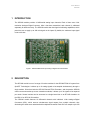
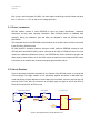
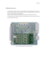
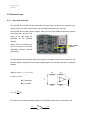
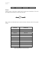
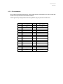
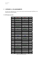
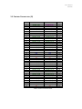
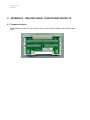
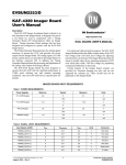
OP5000 Signal Conditioning & I/O Products
for RT-LAB Engineering Simulators
OP5340 Analog to Digital Converter Module
User Manual
Published by
Opal-RT Technologies, Inc.
1751 Richardson, suite 2525
Montréal (Québec) Canada
H3K 1G6
www.opal-rt.com
© 2005 Opal-RT Technologies, Inc.
All rights reserved
Printed in Canada
OP5340_user_manual.doc
Rev.A
User Manual
OP5340
1 INTRODUCTION
The OP5340 module provides 16 differential analog input channels. Each of them uses 16-bit
resolution Analog-to-Digital Converter. After it has been assembled, each channel is calibrated
separately for better accuracy. The OP5340 module has also signal conditioning capabilities, which
permit the user to apply up to 240 volts signal on the inputs. By default, the maximum input signal
is set to 40 volts.
Figure 1: OP5340 Differential Input Analog to Digital Converter Module
2 DESCRIPTION
The OP5340 module is one of a range of function modules for the OP5000 FPGA I/O system from
Opal-RT Technologies. It allows up to 16 analog signals to be sampled simultaneously through a
single module. Given that both the OP5130 External FPGA Processor, and the passive OP5220
carrier can accommodate up to two mezzanine modules; it allows up to 32 signals to be captured
per carrier. Several carriers can be connected to a single board slot on an RT-LAB simulator via
the OP5110 or OP5120 I/O interface.
The OP5340 module features 16 differential channels with individual 16-bit Analog-to-Digital
Converters (ADC), which ensures simultaneous signal capture from multiple channels, thus
eliminating the skew errors associated with multiplexed channels. Each ADC can sample up to 500
User Manual
OP5340
kS/s, giving a total throughput of 8 MS/s. On board signal conditioning provides offsets and gains
from +/- 100 mV to +/- 16 V as well as over-voltage protection.
2.1 OFFSET CALIBRATION
OP5340 module contains a serial EEPROM to store the module identification, calibration
information and any other important information. Each OP5340 module is calibrated after
assembly. During the calibration, gain and offset are adjusted to meet the OP5340 module
specification.
The information stored in the EEPROM can be acceded via an interface when module is connected
to the OP5130 or OP5220 carrier.
RT-LAB, Opal-RT’s simulation software, during the LOAD, reads the EEPROM contents of each
OP5340 (ADC) and OP5330 (DAC) module connected to the OP5110 FPGA PCI board. For each
module, the calibration parameters stored in the EEPROM are used to determine the gain and
offset values of each channel. At run time ADC values are read from the modules and DAC values
to be written to the modules are corrected using these gain and offset values.
2.2 CIRCUIT DIAGRAM
Figure 2 represents a simplified schematic of one channel of the OP5340 module. It is composed
of three stages. First stage consists of one operational amplifier that works in differential input
mode and permits the gain adjustment. Second stage, the level shifter, forms the signal for the A/D
converter input. Then, after the conversion to the digital type, the signal is sent to the OP5110
FPGA PCI board or OP5130 FPGA carrier.
Differential Amplifier
V in
Level Shifter
A / D Converter
+
+
-
VIN
V ref.
-
V ref.
REF
Figure 2: OP5340 Differential Input ADC Module circuit
OUT
Serial Data Out
User Manual
OP5340
2.3 ANALOG INPUT SPECIFICATIONS
2.3.1
TECHNICAL SPECIFICATIONS
Number of channels:
16 differentials
Resolution:
16 bits
Max. Sampling Frequency:
500 kS/s
Min Conversion / Acquisition Time: 2 µs per channel
Type of ADC:
2.3.2
8 x Dual ADC with 10 MBit/s Serial Output Transfer
NOMINAL INPUT RANGES (V)
Positive Full Scale
Negative Full Scale
+120.0
-120.0
+100.0
-100.0
+80.0
-80.0
+60.0
-60.0
+40.0
-40.0
+20.0
-20.0
Hardware default value
2.3.3
2.3.4
DC TRANSFER CHARACTERISTICS
No missing codes resolution:
14 bits min.
Integral nonlinearity (INL):
±8 LSB max.
Differential nonlinearity (DNL):
±1.5 LSB typ. (0 to +70°C)
CMRR:
90 dB
DYNAMIC CHARACTERISTICS
Bandwidth:
Small signal (-3 dB): 820 kHz
Large signal (1% THD): 55 kHz
System noise:
1.8 LSB rms (including quantization)
User Manual
OP5340
2.3.5
CALIBRATION
Programmable gain and offset calibration for each A/D.
Calibration factors are stored in on-board non-volatile memory (flash memory).
2.3.6
Recommended warm-up time:
5 min.
Calibration interval:
as required
PHYSICAL DIMENSIONS
6.73 cm x 12.70 cm (2.65" x 5.00")
I/O connector: 80-pin hi-speed header to carrier
2.3.7
2.3.8
ENVIRONMENTAL
Operating temperature:
0 to 70 °C
Storage temperature:
-55 to 85 °C
Relative humidity:
10 to 90%, no condensing
Maximum altitude:
2,000 m
PIN ASSIGNMENTS
See Appendix A.
User Manual
OP5340
2.4 MODULE INSTALLATION
The OP5340 ADC module can only be used with Opal-RT’s carrier boards type B. The position on
the carrier board is determined by the firmware version of the driving FPGA board. On the same
carrier two modules can be used simultaneously.
The figure 3 shows OP5340 module installed in the section B of the OP5130 active carrier.
Two polarized connectors fasten the module in the suitable position and four screws retain it for the
better connection with the carrier.
Figure 3: OP5340 Differential Input ADC Module position
User Manual
OP5340
2.5 BOARD SETTINGS
2.5.1
INPUT GAIN SELECTION
The OP5340 ADC module has user selectable input gain ability. By default, the maximum input
voltage is set to 40 volts but each channel can be changed separately up to 240 volts.
The OP5340 ADC module contains sockets, which permit to insert additional precision resistors
and change the input gain. The
image on the right shows the
placement
for
the
additional
resistors.
Please, refer to the table at the
Ch00 resistors
position
end of this section for the exact
relationship between channels
and resistors.
The next diagram illustrates input stage of one channel. The default values for the resistors R1 and
R2 were chosen to keep the maximum input voltage range of ±20 volts (40 volts) with no additional
resistors.
Vout full range = ±1 volt (2 volts)
R1
R2
Installed resistors:
V OUT
V IN
R1 = 499 kohms
R2 = 25 kohms
R1
R2
⎛ R2 ⎞
Vout = ⎜
⎟Vin
⎝ R1 ⎠
The surface mount resistors already installed on the OP5340 module give an attenuation of 20.
Vin
1 / 20
Vout
User Manual
OP5340
Input Gain Calculations
Next figure shows the complete circuit with resistor Rx as the axial insertable resistor by the user.
Rx
R1
R2
V IN
V OUT
+
R1
R2
Rx
⎛ R 2 ⎞⎛ Rx ⎞
Vout = ⎜
⎟⎜
⎟Vin
⎝ R1 ⎠⎝ R 2 + Rx ⎠
with already installed on board resistors R1=499k and R2=25k
Vout =
1 ⎛ Rx ⎞
⎜
⎟Vin
20 ⎝ 25 + Rx ⎠
User may define his own input Gain Value and calculate the corresponding Rx resistor value.
Following table gives popular value of maximum ranges and associated Rx resistor values (chosen
in 1% series range). To get the same unit of measurement, the model has to compensate for any
new gain value different from the original gain of 1/20. Last column gives the Gain to insert in the
input signal of the simulation model.
Input
Gain
Max Voltage
Input
Rx value
1% series range
Gain to insert
in the model
1/20
±20V (or 40V)
none
1
1/40
±40V (or 80V)
24.9 kohms
2
1/60
±60V (or 120V)
12.4 kohms
3
1/80
±80V (or 160V)
8.25 kohms
4
1/100
±100V (or 200V)
6.20 kohms
5
User Manual
OP5340
1/120
±120V (or 240V)
4.99 kohms
6
Example:
Added Rx resistor of 4.99 kohms in parallel with R2 resistor gives an attenuation of 120 so the
input voltage can be increase up to ±120 volts (or 240 volts).
Vin
1 / 120
Vout
Table 5 shows the relationship between channel and resistor references used for the input gain
changes.
Channel #
Resistor Rx
Channel 00
R164, R165
Channel 01
R180, R181
Channel 02
R166, R167
Channel 03
R182, R183
Channel 04
R168, R169
Channel 05
R184, R185
Channel 06
R170, R171
Channel 07
R186, R187
Channel 08
R172, R173
Channel 09
R188, R189
Channel 10
R174, R175
Channel 11
R190, R191
Channel 12
R176, R177
Channel 13
R192, R194
Channel 14
R178, R179
Channel 15
R193, R195
Table 5: Relation between channels and resistors
User Manual
OP5340
2.5.2
PIN ASSIGNMENTS
Only external screw terminal board or custom cable that are connected to the carrier board has
access to all input channels of the OP5340 module.
Table 6 gives the pin assignments when using OP5941 (76-pos) Screw Terminal board.
Pos #
Description
Pos #
Description
1
IN 00 +
17
IN 08 +
2
IN 00 -
18
IN 08 -
3
IN 01 +
19
IN 09 +
4
IN 01 -
20
IN 09 -
5
IN 02 +
21
IN 10 +
6
IN 02 -
22
IN 10 -
7
IN 03 +
23
IN 11 +
8
IN 03 -
24
IN 11 -
9
IN 04 +
25
IN 12 +
10
IN 04 -
26
IN 12 -
11
IN 05 +
27
IN 13 +
12
IN 05 -
28
IN 13 -
13
IN 06 +
29
IN 14 +
14
IN 06 -
30
IN 14 -
15
IN 07 +
31
IN 15 +
16
IN 07 -
32
IN 15 -
Table 6: Differential amplifier pin assignment for analog input
User Manual
OP5340
3
APPENDIX A - PIN ASSIGNMENTS
Use these pin assignments only if you are not using the carrier board type B (OP5220) or the
standard screw terminal (OP5941)
3.1 I/O CONNECTORS (J1)
1
3
5
7
9
11
13
15
17
19
21
23
25
27
29
31
33
35
37
39
G1
G3
G5
G7
41
43
45
47
49
51
53
55
57
59
61
63
65
67
69
71
73
75
77
79
SEL_+V
SEL_+V
+12V
NC
EXT_A/B_1
EXT_A/B_2
NC
NC
EXT_A/B_5
EXT_A/B_6
NC
NC
EXT_A/B_9
EXT_A/B_10
NC
NC
EXT_A/B_13
EXT_A/B_14
NC
NC
AGND
AGND
AGND
AGND
EXT_A/B_17
EXT_A/B_18
NC
NC
EXT_A/B_21
EXT_A/B_22
NC
NC
EXT_A/B_25
EXT_A/B_26
NC
NC
EXT_A/B_29
EXT_A/B_30
NC
NC
NC
+12V
SEL_+V
SEL_+V
SEL_-V
SEL_-V
-12V
NC
NC
NC
EXT_A/B_3
EXT_A/B_4
NC
NC
EXT_A/B_7
EXT_A/B_8
NC
NC
EXT_A/B_11
EXT_A/B_12
NC
NC
EXT_A/B_15
EXT_A/B_16
AGND
AGND
AGND
AGND
NC
NC
EXT_A/B_19
EXT_A/B_20
NC
NC
EXT_A/B_23
EXT_A/B_24
NC
NC
EXT_A/B_27
EXT_A/B_28
NC
NC
EXT_A/B_31
EXT_A/B_32
NC
-12V
SEL_-V
SEL_-V
Table 1 I/O Connectors Pinout
2
4
6
8
10
12
14
16
18
20
22
24
26
28
30
32
34
36
38
40
G2
G4
G6
G8
42
44
46
48
50
52
54
56
58
60
62
64
66
68
70
72
74
76
78
80
User Manual
OP5340
3.2 CONTROL CONNECTORS (J2)
1
3
5
7
9
11
13
15
17
19
21
23
25
27
29
31
33
35
37
39
G1
G3
G5
G7
41
43
45
47
49
51
53
55
57
59
61
63
65
67
69
71
73
75
77
79
+5V
MCTRL_A/B_1
MCTRL_A/B_2
MCTRL_A/B_3
MCTRL_A/B_4
MCTRL_A/B_5
+5V
MCTRL_A/B_6
MCTRL_A/B_7
MCTRL_A/B_9
MCTRL_A/B_11
MCTRL_A/B_13
+5V
MCTRL_A/B_15
MCTRL_A/B_17
MCTRL_A/B_19
MCTRL_A/B_20
MCTRL_A/B_21
MCTRL_A/B_23
+5V
GND
GND
GND
GND
+5V
MCTRL_A/B_25
MCTRL_A/B_27
MCTRL_A/B_29
MCTRL_A/B_30
MCTRL_A/B_31
MCTRL_A/B_33
+5V
MCTRL_A/B_35
MCTRL_A/B_37
MCTRL_A/B_39
MCTRL_A/B_40
MCTRL_A/B_42
+5V
MCTRL_A/B_44
MCTRL_A/B_46
MCTRL_A/B_48
MCTRL_A/B_49
MCTRL_A/B_51
+5V
+5V
EEPROM_SCL
EEPROM_SDA
EEPROM_WP
EEPROM_A2
EEPROM_A1
+5V
EEPROM_A0
MCTRL_A/B_8
MCTRL_A/B_10
MCTRL_A/B_12
MCTRL_A/B_14
+5V
MCTRL_A/B_16
MCTRL_A/B_18
CARD_ID_5
CARD_ID_4
MCTRL_A/B_22
MCTRL_A/B_24
+5V
GND
GND
GND
GND
+5V
MCTRL_A/B_26
MCTRL_A/B_28
CARD_ID_3
CARD_ID_2
MCTRL_A/B_32
MCTRL_A/B_34
+5V
MCTRL_A/B_36
MCTRL_A/B_38
CARD_ID_1
MCTRL_A/B_41
MCTRL_A/B_43
+5V
MCTRL_A/B_45
MCTRL_A/B_47
CARD_ID_0
MCTRL_A/B_50
MCTRL_A/B_52
+5V
Table 2 Control Connectors Pinout
2
4
6
8
10
12
14
16
18
20
22
24
26
28
30
32
34
36
38
40
G2
G4
G6
G8
42
44
46
48
50
52
54
56
58
60
62
64
66
68
70
72
74
76
78
80
User Manual
OP5340
4 APPENDIX B - RELATED SIGNAL CONDITIONING PRODUCTS
4.1 TERMINATION PANELS:
Model OP5941 is a dual 38-screw terminal made to connect field I/O signals to the OP53xx module
family.