1
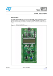
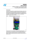
UM0970
User Manual
STM8L-DISCOVERY
Introduction
The STM8L-DISCOVERY helps you to discover the STM8L ultralow power features and to
develop and share your applications. It is based on an STM8L152C6T6 and includes an STLink embedded debug tool interface, LCD (24 segments, 4 commons), LEDs and push
buttons.
Figure 1.
September 2010
STM8L-DISCOVERY board
Doc ID 17693 Rev 1
1/29
www.st.com
Contents
UM0970
Contents
1
Quick start . . . . . . . . . . . . . . . . . . . . . . . . . . . . . . . . . . . . . . . . . . . . . . . . . 3
1.1
Getting started . . . . . . . . . . . . . . . . . . . . . . . . . . . . . . . . . . . . . . . . . . . . . . 3
1.2
System requirements . . . . . . . . . . . . . . . . . . . . . . . . . . . . . . . . . . . . . . . . . 3
1.3
Development toolchain . . . . . . . . . . . . . . . . . . . . . . . . . . . . . . . . . . . . . . . . 4
1.4
Demonstration software . . . . . . . . . . . . . . . . . . . . . . . . . . . . . . . . . . . . . . . 4
1.5
Order code . . . . . . . . . . . . . . . . . . . . . . . . . . . . . . . . . . . . . . . . . . . . . . . . . 4
2
Features . . . . . . . . . . . . . . . . . . . . . . . . . . . . . . . . . . . . . . . . . . . . . . . . . . . 5
3
Hardware and layout . . . . . . . . . . . . . . . . . . . . . . . . . . . . . . . . . . . . . . . . . 6
3.1
STM8L152C6T6 microcontroller . . . . . . . . . . . . . . . . . . . . . . . . . . . . . . . . 9
3.2
Embedded ST-Link . . . . . . . . . . . . . . . . . . . . . . . . . . . . . . . . . . . . . . . . . . 11
3.2.1
Using the ST-Link to program/debug the STM8L on board . . . . . . . . . . 12
3.2.2
Using the ST-Link to program/debug an external STM8L application . . 12
3.3
Power supply and power selection . . . . . . . . . . . . . . . . . . . . . . . . . . . . . . 13
3.4
LEDs . . . . . . . . . . . . . . . . . . . . . . . . . . . . . . . . . . . . . . . . . . . . . . . . . . . . 13
3.5
Push buttons . . . . . . . . . . . . . . . . . . . . . . . . . . . . . . . . . . . . . . . . . . . . . . 13
3.6
Built-in IDD measurement circuit . . . . . . . . . . . . . . . . . . . . . . . . . . . . . . . 14
3.6.1
Run mode . . . . . . . . . . . . . . . . . . . . . . . . . . . . . . . . . . . . . . . . . . . . . . . 14
3.6.2
Low power mode . . . . . . . . . . . . . . . . . . . . . . . . . . . . . . . . . . . . . . . . . . 14
3.6.3
Low power mode IDD measurement principle . . . . . . . . . . . . . . . . . . . . 15
3.6.4
Ibias current measurement procedure . . . . . . . . . . . . . . . . . . . . . . . . . . 16
3.7
Solder bridges . . . . . . . . . . . . . . . . . . . . . . . . . . . . . . . . . . . . . . . . . . . . . 16
3.8
LCD (24 segments, 4 commons) . . . . . . . . . . . . . . . . . . . . . . . . . . . . . . . 17
4
Extension connection . . . . . . . . . . . . . . . . . . . . . . . . . . . . . . . . . . . . . . . 19
5
Electrical schematics . . . . . . . . . . . . . . . . . . . . . . . . . . . . . . . . . . . . . . . 23
6
Revision history . . . . . . . . . . . . . . . . . . . . . . . . . . . . . . . . . . . . . . . . . . . 28
2/29
Doc ID 17693 Rev 1
UM0970
1
Quick start
Quick start
The STM8L-DISCOVERY is a low-cost and easy-to-use development kit to quickly evaluate
and start a development with an STM8L ultralow power microcontroller.
Before installing and using the product, please accept the Evaluation Product License
Agreement from www.st.com/stm8l-discovery.
For more information on the STM8L-DISCOVERY and for demonstration software visit
www.st.com/stm8l-discovery.
1.1
Getting started
1.
Check jumper positions on the board, JP1 and CN3 ON (Discovery selected).
2.
Connect the STM8L-DISCOVERY board to a PC with a USB cable to power the board.
Red LED LD2 (PWR) then lights up.
3.
Function 1 is executed and each click on user button B2 changes the executed function
as described in Table 1.
Table 1.
Functions
Function LED LD3/4
Bars
Value displayed
1
Blink
STM8L VDD voltage measured
2
Off
STM8L consumption measured in Run mode
3
Off
STM8L consumption measured in Low power mode, LCD on
4
Off
STM8L consumption measured in Low power mode, LCD off
5
Off
STM8L consumption measured in Halt mode, LCD off
To study or modify the DISCOVER project related to this demo, visit www.st.com/stm8ldiscovery and follow the tutorial. Discover the STM8L features, download and execute
programs proposed in the list of projects. This site also contains examples from which you
can develop your own applications.
1.2
System requirements
●
Windows PC (2000, XP, Vista)
●
A/Mini-B USB cable
Doc ID 17693 Rev 1
3/29
Quick start
1.3
1.4
UM0970
Development toolchain
●
IAR, Embedded Workbench® for STM8
●
STMicroelectronics, ST Visual Develop (STVD)
Demonstration software
Demonstration software is preloaded in the board's Flash memory. This demonstration uses
the built-in IDD measurement feature of the STM8L-DISCOVERY to automatically measure
and display on the LCD the consumption of the MCU in run and low power modes.
The latest versions of this demonstration source code and associated documentation can
be downloaded from www.st.com/stm8l-discovery.
1.5
Order code
To order the STM8L ultralow power Discovery, use the order code STM8L-DISCOVERY.
4/29
Doc ID 17693 Rev 1
UM0970
2
Features
Features
The STM8L-DISCOVERY offers the following features:
●
STM8L152C6T6 microcontroller, 32 KB Flash, 2 KB RAM, 1 KB EEPROM in 48-pin
LQFP
●
On-board ST-Link with selection mode switch to use the kit as a stand-alone ST-Link
(with SWIM connector for programming and debugging)
●
Two red LEDs; LD1 for USB communication, LD2 for 3.3 V power on
●
Designed to be powered by USB or an external supply of 5 V or 3.3 V
●
Can supply target application with 5 volts and 3 volts
●
Two user LEDs, LD3 and LD4 (green and blue)
●
Two push buttons (User and Reset)
●
IDD current measurement
●
LCD 28-pin DIP (24 segments, 4 commons)
●
Extension header for all QFP48 I/Os for quick connection to prototyping board for easy
probing
Doc ID 17693 Rev 1
5/29
Hardware and layout
3
UM0970
Hardware and layout
The STM8L-DISCOVERY is designed around the STM8L152C6T6 microcontroller in a 48pin LQFP package.
Figure 2 illustrates the connections between the STM8L152C6T6 and its peripherals (STLink, push button, LED, LCD and connectors).
Figure 3 and Figure 4 help you to locate these features on the STM8L-DISCOVERY.
Figure 2.
Hardware block diagram
Mini
USB
SWIM
Embedded
ST-LINK
STM8L152C6T6
I/O
RESET
Green LED
LD3
B1
RST
Blue LED
LD4
B2
USER
IDD
measurement
P2 Header
LCD (24 segments, 4 commons)
6/29
Doc ID 17693 Rev 1
P3 Header
I/O
P1 Header
I/O
UM0970
Figure 3.
Hardware and layout
Top layout
D2 diode
D1 diode
LD2
power
LD1
COM
ST-Link
CN2
SWIM connector
CN3
ST-Link/Discovery
selector
IDD module
LCD 24 segments
JP1
+5V
power supply
input
IDD measurement
+3.3V power supply
input
SB1,2
X2 crystal
STM8L152C6T6
B1
Reset button
B2
User button
LD4
LED blue
LD3
LED green
Doc ID 17693 Rev 1
7/29
Hardware and layout
Figure 4.
UM0970
Bottom layout
SB3,5,7,9
PRG-32
(RESERVED)
SB4,6,8,10
DEFAULT
SB11,12,14
IDD_Measurement
P2
connector
P1
connector
JP1
IDD
SB13,15
X3 crystal
SB17
B2-USER
SB16
B1-RESET
P3
connector
8/29
Doc ID 17693 Rev 1
UM0970
3.1
Hardware and layout
STM8L152C6T6 microcontroller
This 8-bit ultralow power MCU has 32 KB Flash, 2 KB RAM, 1 KB data EEPROM, RTC,
LCD, timers, USART, I2C, SPI, ADC, DAC and comparators.
Figure 5.
STM8L152C6T6 package
The STM8L152C6T6 8-bit microcontroller offers:
32 Kbytes of Flash memory
2 Kbytes RAM
1 Kbytes EEPROM
LQFP48 7 x 7 mm
This device provides the following benefits:
●
Ultralow power proprietary 130 nm technology:
Speed and power consumption independent of MCU power supply, Ultralow leakage
●
Ultralow power design (clock gating, low-power Flash with power-off capability):
Reduced overall Run and Wait mode current consumption by turning off clocks of
unused peripherals or Flash
●
Sub 1 µA hardware RTC and AWU system unit:
Ultralow power modes for applications requesting regular wake up
●
Range of Low power modes (up to 4):
Suitable for many applications from complete switch off to continuous monitoring at
ultralow frequency
●
Advanced and flexible clock system (multiple internal and external clock sources):
Switch and adjust frequency and clock sources on the fly depending on application
needs
●
Direct memory access on board (4-channel DMA):
Autonomy for peripherals, independent from core; can switch off Flash memory and
CPU (large current consumption contributors) while keeping peripherals active
●
Ultralow power and ultrasafe reset system POR/PDR; additional optional activation
BOR:
Integrated safety and security for application
●
Ultrafast wakeup from lowest Low power mode (4 µs):
Fast switching from Static and Dynamic power modes
●
Analog functional down to 1.8 V, programming down to 1.65 V:
Full functionality over the complete VDD range
For more information see the STM8L152C6T6 datasheet (Doc ID 15962) on the ST website.
Doc ID 17693 Rev 1
9/29
Hardware and layout
Figure 6.
10/29
UM0970
STM8L152C6T6 block diagram
Doc ID 17693 Rev 1
UM0970
3.2
Hardware and layout
Embedded ST-Link
The ST-Link programming and debugging tool is integrated on the STM8L-DISCOVERY.
The embedded ST-Link can be used in 2 different ways according to the jumper states (see
Table 2):
●
to program/debug the MCU on board,
●
to program/debug an MCU in an external application board using a cable connected to
SWIM connector CN2.
For information about debugging and programming features refer to ST-Link UM0627.
Note:
UM0627 contains information about all the ST-Link features. Usage in this situation is
restricted to STM8 devices and SWIM support.
Figure 7.
Typical configuration
Hardware requirements:
- USB cable type A to mini-B
- Computer with Windows 2000, XP or Vista OS
Development toolchain:
- IAR, Embedded Workbench® for STM8L
- STMicroelectronics, ST Visual Develop (STVD)
Table 2.
Jumper states
Jumper state
Description
Both CN3 jumpers ON
ST-Link functions enabled for on board programming (default)
Both CN3 jumpers OFF
ST-Link functions enabled for external application through CN2
connector (SWIM supported).
Doc ID 17693 Rev 1
11/29
Hardware and layout
3.2.1
UM0970
Using the ST-Link to program/debug the STM8L on board
To program the STM8L on board, simply plug in the two jumpers on CN3, as shown in
Figure 8 in red, but do not use the CN2 connector as that could disturb communication with
the STM8L152C6T6 of the STM8L-DISCOVERY.
Figure 8.
STM8L-DISCOVERY connections image
Jumpers on CN3
3.2.2
Using the ST-Link to program/debug an external STM8L application
It is very easy to use the ST-Link to program the STM8L on an external application. Simply
remove the 2 jumpers from CN3 as shown in Figure 9, and connect your application to the
CN2 debug connector according to Table 3.
Table 3.
Debug connector CN2 (SWIM)
Pin
12/29
CN2
Designation
1
VDD_TARGET
VDD from application
2
SWIM
SWIM data input/output
3
GND
Ground
4
SWIM_RST
SWIM reset
Doc ID 17693 Rev 1
UM0970
Hardware and layout
Figure 9.
ST-Link connections image
No jumpers on CN3
3.3
Power supply and power selection
The power supply is provided either by the host PC through the USB cable, or by external
power supply (5 V or 3.3 V). The D1 and D2 protection diodes allow the 5V and 3V3 pins to
be used independently as input or output power supplies (see Figure 3). The 5V and 3V3
pins can be used as an output power supply for use by an application board connected on
pin headers (P1 to P3). In such a case, the 3V3 pin provides only a 3V power supply and the
power consumption must be lower than 100 mA. The 5V and 3V3 pins can also be used as
an input power supply for the board when the USB connector is not connected to the PC.
3.4
3.5
LEDs
●
LD1 COM: Red LED indicates communication in progress between PC and ST-Link.
●
LD2 PWR: Red LED indicates that the board is powered.
●
LD3 PE7: Green LED is a user LED connected to the I/O PE7 of the STM8L152C6T6.
●
LD4 PC7: Blue LED is a user LED connected to the I/O PC7 of the STM8L152C6T6.
Push buttons
●
B1 RST: Push button is used to RESET the STM8L152C6T6.
●
B2 USER: User push button connected to the I/O PC1 of the STM8L152C6T6.
Doc ID 17693 Rev 1
13/29
Hardware and layout
3.6
UM0970
Built-in IDD measurement circuit
The STM8L-DISCOVERY built-in IDD measurement circuit allows the consumption of the
STM8L152C6T6 to be measured and displayed on the LCD Glass while the MCU is in Run
or Low power saving modes.
Note:
●
JP1 in ON position: STM8L152C6T6 is powered through IDD measurement circuit
(default).
●
JP1 in OFF position: STM8L152C6T6 is powered directly by +3V3, IDD measurement
circuit is bypassed.
When jumper JP1 is removed the current consumption of the STM8L152C6T6 can be
measured by connecting an ammeter between jumper JP1 pin 1 and pin 2.
For IDD measurement by the MCU itself, the circuit below is implemented on the STM8LDISCOVERY. Solder bridges SB11, SB12 and SB14 must be closed and a jumper must be
plugged between JP1 pin 2 and pin 3.
Figure 10. STM8L-DISCOVERY IDD measurement circuit
IDD
on
3
I/O
O/I
C
GND VCC
R18
2
10K
5
C11
1uF
+3V3
74H1G66STR
D
T1
STT5PF20V
+3V3
5
+3V3
3
2
3
G
0
T2
3
4
S
PF0
R17
SB11
4
IDD_Measurement
+3V3
5
1
2
6
STT5PF20V
G
2K(1%)
U6
5
1
2
6
R21
2(1%)
4
R20
1
4
3
2
4
+3V3
U4
MAX9938FEUK+
S
5
U7
74LX1G04CTR
1
2
3
4
5
6
7
8
U3
Q12 VCC
Q13
Q10
Q14
Q8
Q6
Q9
Q5
CLR
Q7
CI
Q4
CO
GND
CO
D
JP1
1
3
1
off
2
VDD_MCU
C12
100nF
16
15
14
13
12
11
10
9
PE6
SB12
+3V3
R26
10K
PC4
SB14
C13
1nF
M74HC4060TTR
R22
15K
IDD_WAKEUP
R19
47K
IDD_CNT_EN
R23
30K
Oscillator frequency 30KHz
3.6.1
Run mode
In Run mode, IDD current is measured using the operational amplifier MAX9938FEUK+ (U4)
connected to the 2Ω shunt resistor (R20). In this case IDD_CNT_EN remains high during
measurement, so R21 remains in short-circuit during the measurement because of transitor
T1 which remains ON permanently. The jumper JP1 must be connected between pins 2 and
3 of JP1.
3.6.2
Low power mode
In Low power modes (Halt or Active halt), the operational amplifier MAX9938FEUK+ (U4) is
connected to the 2KΩ shunt resistor (R21), controlled by the analogue switch STT5PF20V
(T1). In this case the counter 74HC4060 (U3) enabled by IDD_CNT_EN manages the
measurement timing according to Figure 11.
14/29
Doc ID 17693 Rev 1
UM0970
3.6.3
Hardware and layout
Low power mode IDD measurement principle
The principle used to measure a current when the STM8L152C6T6 is in Low power mode is:
1.
Configure ADC to measure voltage on the IDD_Measurement pin.
2.
Configure PE6 to serve as wakeup pin.
3.
Enter Low power mode after setting IDD_CNT_EN (PC4) signal low.
4.
IDD_WAKEUP rising edge wakes up the MCU after around 300 ms.
5.
Start ADC conversion as soon as possible after wakeup in order to measure the
voltage corresponding to Low power mode on capacitor C11.
6.
Reset the counter by programming IDD_CNT_EN high (in less than 70 ms after the
wakeup) to avoid the R21 2 KΩ resistor being connected later in Run mode.
The measurement timing is given in Figure 11. In Low power modes, the 2 KΩ resistor is
connected when T1 goes off after entering Low power mode. Q13 output of the counter
allows connection of the 2 KΩ resistor when the current IDD becomes very low.
Figure 11 shows how the counter and T1 ensure that, 150 ms after IDD_CNT_EN falling
edge, the shunt resistor R21 is connected between VDD_MCU and the power supply in
order to reduce the measurement range to 30 uA full scale. Then after another 150 ms for
current stabilization, R21 is shorted, the IDD measurement is stored in C11, and the MCU is
woken up. After wakeup the MCU can measure the IDD current corresponding to the Low
power mode stored in C11.
Figure 11. STM8L-DISCOVERY IDD Low power mode measurement timing diagram
The Low power mode measurement procedure can be used in Halt or Active halt mode if the
IDD current does not exceed 30 uA, otherwise the IDD measurement procedure in Run mode
should be used up to 30 mA.
Doc ID 17693 Rev 1
15/29
Hardware and layout
3.6.4
UM0970
Ibias current measurement procedure
In Low power mode the bias current of operational amplifier input (U4 pin 4) is not negligible
compared to IDD current (typical Ibias is ~240 nA). To obtain a reliable STM8L152 IDD
measurement it is mandatory to subtract the bias current from the IDD low power
measurement since this current is not sinked by the MCU. Ibias is measured during
production test and stored in the MCU EPROM. The demonstration software, Discover, uses
this value to display the correct IDD. The Ibias measurement procedure is part of the
demonstration software and can be launched if required.
The procedure for Ibias measurement (implemented in the Demo) is:
1.
Power off the board (disconnect the USB cable).
2.
Set jumper JP1 to OFF position (pins 1 and 2).
3.
Push down B2 (USER button), power on the board from the USB.
4.
Wait at least 1 second before releasing B2, the LCD displays the Ibias measurement.
5.
Power off the board (disconnect the USB cable).
6.
Set jumper JP1 to ON position (pins 2 and 3). The Ibias value is now stored. The bias
current is then subtracted from the IDD measurement performed in Low power mode.
3.7
Solder bridges
Table 4.
Solder bridge
Bridge
State(1)
Description
Off
PA2, PA3 are disconnected from P1
X2, C19, C20 and R24 provide a clock as shown in schematics
On
PA2, PA3 are connected to P1 (X2, C19, C20, R24 must not be fitted)
SB3,5,7,9
(DEFAULT)
On
Reserved, do not modify
SB4,6,8,10
(PRG-32)
Off
Reserved, do not modify
Off
PFO, PE6, PC4 are available and IDD module cannot be used
JP1 must be set to OFF
On
PFO, PE6, PC4 are used by IDD module
JP1 must be set to ON
SB13,15
(X3 crystal)
Off
PC5, PC6 are only connected to P2 (but do not remove X3, C21, C23, R27)
On
PC5, PC6 are connected to P2. X3, C21, C23 and R27 provide 32 KHz clock
SB16
(B1-RESET)
Off
PA1/RESET signal is only connected to P1
On
PA1/RESET signal is used by ST_LINK as SWIM_RST and also connected to P1
SB17
(B2-USER)
Off
PC1 is only connected to P2
On
PC1 is connected to P2 and push button B2 for user
SB1,2
(X2 crystal)
SB11,12,14
(IDD_Measurement)
1. Default state is in bold type.
16/29
Doc ID 17693 Rev 1
UM0970
3.8
Hardware and layout
LCD (24 segments, 4 commons)
This LCD allows the STM8L152C6T6 to display any information on six 14-segment digits
and 4 BARs, using all COMs. (See the LCD segment mapping in Figure 12 and pin
connections in Table 5.)
Note:
This LCD also supports six 8-segment digits by only using COM0 and COM1.
This configuration allows COM2 and COM3 to be used as I/O ports. In this case the 2 LCD
pins must not be plugged into the LCD socket. To proceed with this configuration, remove
the LCD carefully, slightly open the COM2 and COM3 pins (pin 13 and pin 14) of the LCD,
then replug it in the socket.
Characteristics overview:
Note:
●
24 segments and 4 commons
●
Drive method: multiplexed 1/4 duty, 1/3 bias
●
Operating voltage: 3 V
●
Operating temperature: 0 to 50°C
●
Connector: 28-pin DIL 2.54 mm pitch
When the LCD is plugged, all I/O ports listed in Table 5 are unavailable. To use one of these
as I/O, you must remove the LCD.
Figure 12. LCD segment mapping
Doc ID 17693 Rev 1
17/29
Hardware and layout
Table 5.
UM0970
LCD connections
STM8L152C6T6
Pin name
18/29
LCD
Pin
COM3
COM2
COM1
COM0
PA7_LCDSEG0
1
1N
1P
1D
1E
PE0_LCDSEG1
2
1DP
1COLON
1C
1M
PE1_LCDSEG2
3
2N
2P
2D
2E
PE2_LCDSEG3
4
2DP
2COLON
2C
2M
PE3_LCDSEG4
5
3N
3P
3D
3E
PE4_LCDSEG5
6
3DP
3COLON
3C
3M
PE5_LCDSEG6
7
4N
4P
4D
4E
PD0_LCDSEG7
8
4DP
4COLON
4C
4M
PD2_LCDSEG8
9
5N
5P
5D
5E
PD3_LCDSEG9
10
BAR2
BAR3
5C
5M
PB0_LCDSEG10
11
6N
6P
6D
6E
PB1_LCDSEG11
12
BAR0
BAR1
6C
6M
PD1_LCDCOM3
13
COM3
PA6_LCDCOM2
14
PA5_LCDCOM1
15
PA4_LCDCOM0
16
PB2_LCDSEG12
17
6J
6K
6A
6B
PB3_LCDSEG13
18
6H
6Q
6F
6G
PB4_LCDSEG14
19
5J
5K
5A
5B
PB5_LCDSEG15
20
5H
5Q
5F
5G
PB6_LCDSEG16
21
4J
4K
4A
4B
PB7_LCDSEG17
22
4H
4Q
4F
4G
PD4_LCDSEG18
23
3J
3K
3A
3B
PD5_LCDSEG19
24
3H
3Q
3F
3G
PD6_LCDSEG20
25
2J
2K
2A
2B
PD7_LCDSEG21
26
2H
2Q
2F
2G
PC2_LCDSEG22
27
1J
1K
1A
1B
PC3_LCDSEG23
28
1H
1Q
1F
1G
COM2
COM1
COM0
Doc ID 17693 Rev 1
Extension connection
4
UM0970
Extension connection
Male headers P1, P2 and P3 can connect the STM8L-DISCOVERY to a standard
prototyping/wrapping board. All GPI/Os of STM8L152C6T6 are available on it.
P1, P2 and P3 can also be probed by an oscilloscope, logical analyzer or voltmeter.
P1 pinout
Pin number Pin number
(P1)
(STM8L)
1
Main
function
Alternate function
LCD (U5)
3.3 V board power
supplied or supply
external application when
USB connected
+3V3
1
PA0
3
9/40
GND
4
2
PA1
I/O Reset
NRST/PA1(1)
5
3
PA2
I/O Port A2
PA2/OSC_IN/
[USART1_TX](3)/
[SPI1_MISO] (3)
6
4
PA3
I/O Port A3
PA3/OSC_OUT/
[USART1 _RX](3)/
[SPI1_MOSI](3)
I/O Port A4
PA4/TIM2_BKIN/
LCD_COM0(2)/
ADC1_IN2/
COMP1_INP
LCD_COM0
I/O Port A5
PA5/TIM3_BKIN/
LCD_COM1(2)/
ADC1_IN1/
COMP1_INP
LCD_COM1
LCD_COM2
8
5
6
PA4
PA5
I/O Port A0
PA0/[USART1_CK](3)/
SWIM/BEEP/
IR_TIM (7)
2
7
19/29
Board pin
name
Type
Table 6.
Ground
9
7
PA6
I/O Port A6
PA6/[ADC1_TRIG](3)/
LCD_COM2(2)/
ADC1_IN0/
COMP1_INP
10
8
PA7
I/O Port A7
PA7/
LCD_SEG0(2)(4)
LCD_SEG0
11
14
PE0
I/O Port E0
PE0(4)/
LCD_SEG1(2)
LCD_SEG1
12
15
PE1
I/O Port E1
PE1/TIM1_CH2N /
LCD_SEG2(2)
LCD_SEG2
13
16
PE2
I/O Port E2
PE2/TIM1_CH3N /
LCD_SEG3(2)
LCD_SEG3
14
17
PE3
I/O Port E3
PE3/LCD_SEG4(2)
LCD_SEG4
15
18
PE4
I/O Port E4
PE4/LCD_SEG5(2)
LCD_SEG5
Doc ID 17693 Rev 1
UM0970
Extension connection
Pin number Pin number
(P1)
(STM8L)
16
17
19
20
Board pin
name
PE5
PD0
18
21
PD1
19
9/40
GND
Table 7.
Type
P1 pinout (continued)
Main
function
Alternate function
I/O Port E5
LCD_SEG6
I/O Port D0
PD0/TIM3_CH2/
[ADC1_TRIG](3)/
LCD_SEG7(2)/
ADC1_IN2 2/
COMP2_INP/
COMP1_INP
LCD_SEG7
I/O Port D1
PD1/TIM3_TRIG/
LCD_COM3(2)/
ADC1_IN21/
COMP2_INP/
COMP1_INP
LCD_COM3
Ground
P2 pinout
Pin number Pin number
(P2)
(STM8L)
Pin name
1
+5V
2
NC
Main
function
Alternate function
9/40
GND
4
48
PE7
I/O Port E7
PE7/LCD_SEG27(2)
5
47
PE6
I/O Port E6
PE6/LCD_SEG26(2)/
PVD_IN
Ground
6
46
PC7
I/O Port C7
PC7/LCD_SEG25(2)/
ADC1_IN3/
COMP2_INM/
COMP1_INP
7
45
PC6
I/O Port C6
PC6/OSC32_OUT/
[SPI1_SCK](3)/
[USART1_RX](3)
8
44
PC5
I/O Port C5
PC5/OSC32_IN /
[SPI1_NSS](3)/
[USART1_TX](3)
I/O Port C4
PC4/[USART1_CK](3)/
I2C1_SMB/CCO/
LCD_SEG24(2)/
ADC1_IN4/COMP2_INM/
COMP1_INP
43
PC4
LCD (U5)
5 Volts board power
supplied or supply
external application when
USB connected
3
9
LCD (U5)
PE5/LCD_SEG6(2)/
ADC1_IN23/
COMP2_INP/
COMP1_INP
Type
Table 6.
Doc ID 17693 Rev 1
20/29
UM0970
Extension connection
P2 pinout (continued)
Pin number Pin number
(P2)
(STM8L)
10
42
Pin name
PC3
Type
Table 7.
Main
function
Alternate function
LCD (U5)
I/O Port C3
PC3/[USART1_TX](3)/
LCD_SEG23(2)/
ADC1_IN5/
COMP1_INP/
COMP2_INM
LCD_SEG23
LCD_SEG22
11
41
PC2
I/O Port C2
PC2/[USART1_RX](3)/
LCD_SEG22/
ADC1_IN6/
COMP1_INP/
VREF_OUT
12
38
PC1
I/O Port C1
PC1(4)/I2C1_SCL
13
37
PC0
I/O Port C0
PC0(4)/I2C1_SDA
I/O Port D7
PD7/TIM1_CH1N /
LCD_SEG21(2)/
ADC1_IN7/
RTC_ALARM/
VREF_OUT/
COMP1_INP
LCD_SEG21
I/O Port D6
PD6/TIM1_BKIN /
LCD_SEG20(2)/
ADC1_IN8/
RTC_CALIB/
VREF_OUT/
COMP1_INP
LCD_SEG20
I/O Port D5
PD5/TIM1_CH3 /
LCD_SEG19(2)/
ADC1_IN9/
COMP1_INP
LCD_SEG19
LCD_SEG18
14
15
16
36
35
34
PD7
PD6
PD5
17
33
PD4
I/O Port D4
PD4/TIM1_CH2 /
LCD_SEG18(2)/
ADC1_IN10/
COMP1_INP
18
32
PF0
I/O Port F0
PF0/ADC1_IN24/
DAC_OUT
19
9/40
GND
Doc ID 17693 Rev 1
Ground
21/29
Extension connection
P3 pinout
Pin number Pin number
(P3)
(STM8L)
1
2
3
4
5
6
7
8
9
10
22/29
22
23
24
25
26
27
28
29
30
31
Pin name
PD2
PD3
PB0
PB1
PB2
PB3
PB4
PB5
PB6
PB7
Type
Table 8.
UM0970
Main
function
Alternate function
LCD (U5)
I/O Port D2
PD2/TIM1_CH1 /
LCD_SEG8(2)/
ADC1_IN20/
COMP1_INP
LCD_SEG8
I/O Port D3
PD3/ TIM1_TRIG/
LCD_SEG9(2)/
ADC1_IN1 9/
COMP1_INP
LCD_SEG9
I/O Port B0
PB0/TIM2_CH1/
LCD_SEG10(2)/
ADC1_IN18/
COMP1_INP
LCD_SEG10
I/O Port B1
PB1/TIM3_CH1/
LCD_SEG11(2)/
ADC1_IN17/
COMP1_INP
LCD_SEG11
I/O Port B2
PB2/ TIM2_CH2/
LCD_SEG12(2)/
ADC1_IN16/
COMP1_INP
LCD_SEG12
I/O Port B3
PB3/TIM2_TRIG/
LCD_SEG13(2)/
ADC1_IN15/
COMP1_INP
LCD_SEG13
I/O Port B4
PB4/[SPI1_NSS](3)/
LCD_SEG14(2)/
ADC1_IN14/
COMP1_INP
LCD_SEG14
I/O Port B5
PB5/[SPI1_SCK](3)/
LCD_SEG15(2)/
ADC1_IN13/
COMP1_INP
LCD_SEG15
I/O Port B6
PB6/[SPI1_MOSI](3)/
LCD_SEG16(2)/
ADC1_IN12/
COMP1_INP
LCD_SEG16
I/O Port B7
PB7/[SPI1_MISO](3)/
LCD_SEG17(2)/
ADC1_IN11/
COMP1_INP
LCD_SEG17
Doc ID 17693 Rev 1
Electrical schematics
Electrical schematics
23/29
5
Figure 13. STM8L-DISCOVERY
IDD_measurement.SchDoc
U_Power
ST_LINK.SCHDOC
U_ST_LINK
P2
IDD_CNT_EN
IDD_Measurement
IDD_WAKEUP
IDD_CNT_EN
IDD_Measurement
IDD_WAKEUP
RESET#
ST_LINK_SWIM
EXT_5V
EXT_3V3
MCU.SchDoc
U_MCU
Doc ID 17693 Rev 1
PA[0..7]
PB[0..7]
PC[0..7]
PD[0..7]
PE[0..7]
PF0
RESET#
ST_LINK_SWIM
P1
1
2
3
4
5
6
7
8
9
10
11
12
13
14
15
16
17
18
19
Header 19
EXT_3V3
PA0
PA1 RST
PA2
PA3
PA4
PA5
PA6
PA7
PE0
PE1
PE2
PE3
PE4
PE5
PD0
PD1
IDD_CNT_EN
IDD_Measurement
IDD_WAKEUP
EXT_5V
PE7
PE6
PC7
PC6
PC5
PC4
PC3
PC2
PC1
PC0
PD7
PD6
PD5
PD4
PF0
GH08172_buttons.SchDoc
U_Power
PA[0..7]
PB[0..7]
PC[0..7]
PD[0..7]
PE[0..7]
PF0
RESET#
ST_LINK_SWIM
RESET#
ST_LINK_SWIM
EXT_5V
EXT_3V3
IDD_CNT_EN
IDD_Measurement
IDD_WAKEUP
PC3_LCDSEG23
PC2_LCDSEG22
PD7_LCDSEG21
PD6_LCDSEG20
PD5_LCDSEG19
PD4_LCDSEG18
PB7_LCDSEG17
PB6_LCDSEG16
PB5_LCDSEG15
PB4_LCDSEG14
PB3_LCDSEG13
PB2_LCDSEG12
PB1_LCDSEG11
PB0_LCDSEG10
PD3_LCDSEG9
PD2_LCDSEG8
PD0_LCDSEG7
PE5_LCDSEG6
PE4_LCDSEG5
PE3_LCDSEG4
PE2_LCDSEG3
PE1_LCDSEG2
PE0_LCDSEG1
PA7_LCDSEG0
PD1_LCDCOM3
PA6_LCDCOM2
PA5_LCDCOM1
PA4_LCDCOM0
1
2
3
4
5
6
7
8
9
10
11
12
13
14
15
16
17
18
19
Header 19
P3
Header 10
PD2
PD3
PB0
PB1
PB2
PB3
PB4
PB5
PB6
PB7
STMicroelectronics
Title:
STM8L-DISCOVERY
Number:MB913
Rev: B.2(PCB.SCH)
Date: 7/15/2010
Sheet 1
of
5
UM0970
1
2
3
4
5
6
7
8
9
10
Electrical schematics
LCD
15
COM1
COM2
16
COM0
COM3
17
17
12
U5
GH08172T
14
13
12
18
18
19
19
10
11
11
20
20
21
21
8
9
9
8
22
22
23
23
6
7
7
24
24
5
PA7_LCDSEG0
PE0_LCDSEG1
PE1_LCDSEG2
PE2_LCDSEG3
PE3_LCDSEG4
PE4_LCDSEG5
PE5_LCDSEG6
PB6_LCDSEG16
PB5_LCDSEG15
PB4_LCDSEG14
PB3_LCDSEG13
PB2_LCDSEG12
PA4_LCDCOM0
PA5_LCDCOM1
6
5
25
25
26
26
3
27
27
2
4
4
3
28
1
1
Doc ID 17693 Rev 1
2
28
PB7_LCDSEG17
PD4_LCDSEG18
PD5_LCDSEG19
PD6_LCDSEG20
PD7_LCDSEG21
PC2_LCDSEG22
PC3_LCDSEG23
10
24/29
Figure 14. LCD
PA6_LCDCOM2
PD1_LCDCOM3
PB1_LCDSEG11
PB0_LCDSEG10
PD3_LCDSEG9
PD2_LCDSEG8
PD0_LCDSEG7
STMicroelectronics
Title:
STM8L-DISCOVERY LCD
Number:MB915
Rev: B.2(SCH.PCB)
Date: 7/15/2010
Sheet 2
of
5
UM0970
UM0970
Figure 15. IDD measurement
IDD
VDD_MCU
U4
MAX9938FEUK+
3
1
4
3
4
R21
2(1%)
2K(1%)
2
R20
R18
2
10K
5
C11
1uF
+3V3
3
4
T1
STT5PF20V
0
+3V3
4
+3V3
T2
3
D
G
IDD_Measurement
SB11
74H1G66STR
5
+3V3
3
Doc ID 17693 Rev 1
2
S
PF0
R17
5
1
2
6
4
+3V3
I/O
O/I
C
GND VCC
S
U6
5
U7
74LX1G04CTR
Q12 VCC
Q13
Q10
Q14
Q8
Q6
Q9
Q5
CLR
Q7
CI
Q4
CO
GND
CO
M74HC4060TTR
5
1
2
6
STT5PF20V
C12
100nF
U3
1
2
3
4
5
6
7
8
G
JP1
D
1
2
on
3
1
off
16
15
14
13
12
11
10
9
PE6
IDD_WAKEUP
SB12
+3V3
R19
47K
R26
10K
PC4
IDD_CNT_EN
SB14
C13
1nF
R22
15K
R23
30K
Oscillator frequency 30KHz
25/29
Title:
STM8L-DISCOVERY IDD_Measurement
Number:MB915
Rev: B.2(SCH.PCB)
Date: 7/15/2010
Sheet 3
Electrical schematics
STMicroelectronics
LD3
R28
PE7
330
green
ST_LINK_SWIM
660
3
SB16
1
Must be close to the Crystal and ON
C24
100nF
X3
C21
6.8pF
4
B1
RESET (Black)
1
R27
0
U8
Doc ID 17693 Rev 1
X2
16MHz
PA4
PA5
PA6
PA7
PA4_LCDCOM0
PA5_LCDCOM1
PA6_LCDCOM2
PA7_LCDSEG0
PA3
SB1
R24
60
VDD_MCU
VDDA
R25
VDD_MCU
0
Not Fitted
C22
1uF
PE0
PE1
PE2
PE3
PE4
PE5
PD0
PD1
PD2
PD3
PB0
PE0_LCDSEG1
PE1_LCDSEG2
PE2_LCDSEG3
PE3_LCDSEG4
PE4_LCDSEG5
PE5_LCDSEG6
PD0_LCDSEG7
PD1_LCDCOM3
PD2_LCDSEG8
PD3_LCDSEG9
PB0_LCDSEG10
PA0
PA1
PA2
PA3
PA4
PA5
PA6
PA7
AVSS
VDD
VDDA
VREF+
VLCD
PE0
PE1
PE2
PE3
PE4
PE5
PD0
PD1
PD2
PD3
PB0
PE7
PE6
PC7
PC6
PC5
PC4
PC3
PC2
VSSIO
VDDIO
PC1
PC0
PD7
PD6
PD5
PD4
PF0
PB7
PB6
PB5
PB4
PB3
PB2
PB1
48
47
46
45
44
43
42
41
40
39
38
37
36
35
34
33
32
31
30
29
28
27
26
25
PE7
PE6
PC7
PC6
PC5
PC4
PC3
PC2
PC1
PC0
PD7
PD6
PD5
PD4
PF0
PB7
PB6
PB5
PB4
PB3
PB2
PB1
Must be close to the Crystal and ON
IDD_WAKEUP
SB13
IDD_CNT_EN
PC3_LCDSEG23
PC2_LCDSEG22
SB15
+3V3
User Button
VDD_MCU
R30
4K7
User_PB
SB17
PD7_LCDSEG21
PD6_LCDSEG20
PD5_LCDSEG19
PD4_LCDSEG18
3
20pF
1
2
3
4
5
6
7
8
9
10
11
12
13
14
15
16
17
18
19
20
21
22
23
24
2
PA0
PA1
SB2
B2
USER (Blue)
IDD_Measurement
PB7_LCDSEG17
PB6_LCDSEG16
PB5_LCDSEG15
PB4_LCDSEG14
PB3_LCDSEG13
PB2_LCDSEG12
PB1_LCDSEG11
4
PA2
1
Not Fitted
PA[0..7]
PB[0..7]
PC[0..7]
PD[0..7]
PE[0..7]
PF0
3
MC306-G-06Q-32.768 (manufacturer JFVNY)
C20
20pF
C23
6.8pF
4
2
C19
blue
RESET#
2
RESET#
LD4
R29
PC7
RESET
Electrical schematics
26/29
Figure 16. STM8L MCU
C25
100nF
SWIM
STM8L152C6T6
PA[0..7]
PB[0..7]
PC[0..7]
PD[0..7]
PE[0..7]
PF0
VDD_MCU
C18
1uF
C17
100nF
C16
100nF
VDDA
L1
BEAD
C14
1uF
C15
100nF
STMicroelectronics
Title:
LED
Number:MB915
Rev: B.2(PCB.SCH)
Date: 7/15/2010
Sheet 4
of
5
UM0970
STM8L-DISCOVERY MCU
ST_LINK_SWIM
RESET#
R12
SWIM_IN
R13
SWIM
48
47
46
45
44
43
42
41
40
39
38
37
220
1
2
C8
20pF
+3V3
8MHz
1
2
3
4
SWIM_PULLUP_CTL
5
OSC_IN
OSC_OUT 6
STM_RST 7
8
C10
9
100nF+3V3 AIN_1 10
M25_CS 11
U2_TX 12
R14
+3V3
100K
R16
4K7
SWIM_RST_IN
36
35
34
33
32
31
30
29
28
27
26
25
47
R7
R6
SWIM_RST
220
+3V3
VDD_2
VSS_2
JTMS
PA12
PA11
PA10
PA9
PA8
S2_MOSI
S2_MISO
S2_CK
PB12
13
14
15
16
17
18
19
20
SWIM_IN 21
22
SWIM
23
24
R15
4K7
VBAT
PC13
PC14
PC15
OSC_IN
OSC_OUT
/RST
VSSA
VDDA
PA0
PA1
U2_TX
U2_RX
U2_CK
T_JTCK
T_JTDO
T_JTDI
T_NRST
T_JRST
STM_JTMS
USB_DP
USB_DM
U1_RX
U1_TX
ST_LINK_LED
47
SB4
SB3
SB6
SB5
SB8
SB7
SB10
SB9
+3V3
STM_JTCK
SWCLK
STM_JTMS
SWDIO
CN2
1
2
3
4
SWIM
R11
10K
DISCOVERY
ST-LINK
CN3
T_JTMS
T_JTCK
Jumpers ON --> DISCOVERY Selected
Jumpers OFF --> ST-LINK Selected
Wired on Solder Side
JP3
COM
JP2
+3V3
ST_LINK_LED
R8
510
EXT_5V
D2
+5V
U5V
U1
+5V
BAT60JFILM
3
R3
1K5
C3
10uF
CN1
R5
22
R4
RED
D1
BAT60JFILM
LD1117S33TR
2
Vin
Vout
R1
1K
C1
10uF
USB_DM
USB_DP
LD2
RED
C2
100nF
+3V3
EXT_3V3
22
R2
100K
+3V3
5075BMR-05-SM
USB
C5
100nF
C6
100nF
C7
100nF
C4
100nF
STMicroelectronics
Title:
STM8L-DISCOVERY ST-LINK (SWIM only)
Number:MB915
Rev: B.2(PCB.SCH)
Date: 7/15/2010
Sheet 5
of
5
27/29
Electrical schematics
VCC
DD+
ID
GND
SHELL
1
2
3
4
5
0
LD1
PWR
U5V
+3V3
1
Doc ID 17693 Rev 1
+3V3
VDD_3
VSS_3
PB9
PB8
BOOT0
PB7
PB6
PB5
JNRST
JTDO
JTDI
JTCK
X1
U2_RX
U2_CK
S1_CK
S1_MISO
S1_MOSI
PB0
PB1
PB2/BOOT1
PB10
PB11
VSS_1
VDD_1
C9
20pF
U2
STM32F103C8T6
PRG-32
R10
680
1
2
3
4
+3V3
+3V3
SWIM_IN
SWIM_RST
SWIM_RST_IN
STM_JRST
STM_JTDO
STM_JTDI
STM_JTCK
SWIM_IN
SWIM
100K
DEFAULT
R9
UM0970
Figure 17. ST-Link (SWIM only)
Revision history
6
UM0970
Revision history
Table 9.
28/29
Document revision history
Date
Revision
24-Sep-2010
1
Changes
Initial release.
Doc ID 17693 Rev 1
UM0970
Please Read Carefully:
Information in this document is provided solely in connection with ST products. STMicroelectronics NV and its subsidiaries (“ST”) reserve the
right to make changes, corrections, modifications or improvements, to this document, and the products and services described herein at any
time, without notice.
All ST products are sold pursuant to ST’s terms and conditions of sale.
Purchasers are solely responsible for the choice, selection and use of the ST products and services described herein, and ST assumes no
liability whatsoever relating to the choice, selection or use of the ST products and services described herein.
No license, express or implied, by estoppel or otherwise, to any intellectual property rights is granted under this document. If any part of this
document refers to any third party products or services it shall not be deemed a license grant by ST for the use of such third party products
or services, or any intellectual property contained therein or considered as a warranty covering the use in any manner whatsoever of such
third party products or services or any intellectual property contained therein.
UNLESS OTHERWISE SET FORTH IN ST’S TERMS AND CONDITIONS OF SALE ST DISCLAIMS ANY EXPRESS OR IMPLIED
WARRANTY WITH RESPECT TO THE USE AND/OR SALE OF ST PRODUCTS INCLUDING WITHOUT LIMITATION IMPLIED
WARRANTIES OF MERCHANTABILITY, FITNESS FOR A PARTICULAR PURPOSE (AND THEIR EQUIVALENTS UNDER THE LAWS
OF ANY JURISDICTION), OR INFRINGEMENT OF ANY PATENT, COPYRIGHT OR OTHER INTELLECTUAL PROPERTY RIGHT.
UNLESS EXPRESSLY APPROVED IN WRITING BY AN AUTHORIZED ST REPRESENTATIVE, ST PRODUCTS ARE NOT
RECOMMENDED, AUTHORIZED OR WARRANTED FOR USE IN MILITARY, AIR CRAFT, SPACE, LIFE SAVING, OR LIFE SUSTAINING
APPLICATIONS, NOR IN PRODUCTS OR SYSTEMS WHERE FAILURE OR MALFUNCTION MAY RESULT IN PERSONAL INJURY,
DEATH, OR SEVERE PROPERTY OR ENVIRONMENTAL DAMAGE. ST PRODUCTS WHICH ARE NOT SPECIFIED AS "AUTOMOTIVE
GRADE" MAY ONLY BE USED IN AUTOMOTIVE APPLICATIONS AT USER’S OWN RISK.
Resale of ST products with provisions different from the statements and/or technical features set forth in this document shall immediately void
any warranty granted by ST for the ST product or service described herein and shall not create or extend in any manner whatsoever, any
liability of ST.
ST and the ST logo are trademarks or registered trademarks of ST in various countries.
Information in this document supersedes and replaces all information previously supplied.
The ST logo is a registered trademark of STMicroelectronics. All other names are the property of their respective owners.
© 2010 STMicroelectronics - All rights reserved
STMicroelectronics group of companies
Australia - Belgium - Brazil - Canada - China - Czech Republic - Finland - France - Germany - Hong Kong - India - Israel - Italy - Japan Malaysia - Malta - Morocco - Philippines - Singapore - Spain - Sweden - Switzerland - United Kingdom - United States of America
www.st.com
Doc ID 17693 Rev 1
29/29