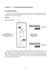
1
DIO-24 DIO-96/144 User Manual Version 2.4 Nov. 2011 Warranty All products manufactured by ICP DAS are warranted against defective materials for a period of one year from the date of delivery to the original purchaser. Warning ICP DAS assumes no liability for damages consequent to the use of this product. ICP DAS reserves the right to change this manual at any time without notice. The information furnished by ICP DAS is believed to be accurate and reliable. However, no responsibility is assumed by ICP DAS for its use, nor for any infringements of patents or other rights of third parties resulting from its use. Copyright Copyright © 2011 by ICP DAS. All rights are reserved. Trademark Names are used for identification only and may be registered trademarks of their respective companies. DIO-D24/DIO-96/DIO-144 User Manual (Ver.2.4, Nov. 2011, IMH-007-24) 1 Tables of Contents DIO-24 24-BIT COMPATIBLE DIO OPTO-22 BOARD.......................................................4 1. INTRODUCTION ..............................................................................................................4 1.1 FEATURES ......................................................................................................................4 1.2 APPLICATIONS ...............................................................................................................4 1.3 SPECIFICATIONS ............................................................................................................5 1.4 PRODUCT CHECK LIST ..................................................................................................6 2. HARDWARE CONFIGURATION ..................................................................................7 2.1 BOARD LAYOUT ............................................................................................................7 2.2 JUMPER SETTING ...........................................................................................................8 2.2.1 Interrupt Jumper Setting.............................................................................................8 2.2.2 Interrupt Status Setting ...............................................................................................8 2.2.3 Interrupt Trigger Edge Setting ...................................................................................8 2.3 BASE ADDRESS SETTING ...............................................................................................9 2.4 PIN ASSIGNMENTS .......................................................................................................13 3. PROGRAMMING ...........................................................................................................15 3.1 REGISTER ....................................................................................................................15 3.2 INTERRUPT HANDLING ................................................................................................17 3.3 OUTPUT LATCH ...........................................................................................................17 3.4 PROGRAM EXAMPLE ...................................................................................................18 4. SOFTWARE/HARDWARE INSTALLATION.............................................................19 4.1 SOFTWARE INSTALLING PROCEDURE .........................................................................19 4.2 HARDWARE INSTALLING PROCEDURE ........................................................................20 DIO-96/DIO-144 96/144-BIT OPTO-22 COMPATIBLE DIO BOARD........................23 5. SOFTWARE INSTALLATION .......................................................................................23 5.1 FEATURES....................................................................................................................23 5.2 APPLICATIONS .............................................................................................................23 5.3 SPECIFICATIONS ..........................................................................................................24 5.4 PRODUCT CHECK LIST ................................................................................................25 6. HARDWARE CONFIGURATION .....................................................................................26 6.1 BOARD LAYOUT ..........................................................................................................26 6.2 JUMPER SETTING .........................................................................................................27 DIO-D24/DIO-96/DIO-144 User Manual (Ver.2.4, Nov. 2011, IMH-007-24) 2 6.2.1 Interrupt Jumper Setting...........................................................................................27 6.2.2 Interrupt Status Setting .............................................................................................27 6.2.3 96-bit/144-bit Jumper Setting ...................................................................................27 6.3 BASE ADDRESS SETTING .............................................................................................28 6.3.1 96-bit Mode............................................................................................................28 6.3.2 144-bit Mode...........................................................................................................30 6.4 PIN ASSIGNMENTS .......................................................................................................32 7. PROGRAMMING ...........................................................................................................34 7.1 REGISTER ....................................................................................................................34 7.2 DATA FORMAT ............................................................................................................36 7.3 INTERRUPT HANDLING ................................................................................................38 7.4 OUTPUT LATCH ...........................................................................................................38 7.5 PROGRAM EXAMPLE ...................................................................................................39 8. SOFTWARE/HARDWARE INSTALLATION.............................................................40 8.1 SOFTWARE INSTALLING PROCEDURE ..........................................................................40 8.2 HARDWARE INSTALLING PROCEDURE .........................................................................41 APPENDIX: DAUGHTER BOARD.........................................................................................44 A1. DAUGHTER BOARD COMPARISON TABLE ...................................................................44 A2. DB-24P/24PD ISOLATED INPUT BOARD .....................................................................45 A3. DB-24R/24RD RELAY BOARD....................................................................................46 A4. DB-24PR/24PRD ........................................................................................................47 DIO-D24/DIO-96/DIO-144 User Manual (Ver.2.4, Nov. 2011, IMH-007-24) 3 DIO-24 24-bit Compatible DIO OPTO-22 Board 1. Introduction The DIO-24 provides 24 TTL digital I/O lines. The DIO-24 emulates 8255 mode 0 and has an increased output current of 15 mA (source) and 64 mA (sink) , allowing it to control LED, relay, etc. The DIO-24 consists of three 8 bit bidirectional ports and 2 input lines for interrupt enable and interrupt. The 8 bit ports are named port A(PA),port B(PB) and port C(PC). The port C can be split into two four bit. All ports are configured as inputs upon power-up or reset. The DIO-24 uses 4 consecutive I/O locations in I/O addressing space. The base address is selectable from 200 to 3FF hex. The interrupt signal can be connected to any of the interrupt levels 2 through 7. 1.1 Features 24 digital I/O lines Emulate 8255 mode (Basic input/output mode) Buffer output for higher driving capability than 8255 Register compatible to 724 series Programmable interrupt handling Output status readback 1.2 Applications Interfacing with any OPTO-22 compatible I/O module Digital I/O control Contact closure monitoring and alarm monitoring Useful with parallel interface devices DIO-D24/DIO-96/DIO-144 User Manual (Ver.2.4, Nov. 2011, IMH-007-24) 4 1.3 Specifications Model Name DIO-24 Digital Input Channels 24 (OPTO-22 compatible) Compatibility 5 V/TTL Input Voltage Logic 0: 0.8 V max. Logic 1: 2.0 V min. Response Speed 1.0 MHz (Typical) Digital Output Channels 24 (OPTO-22 compatible) Compatibility 5 V/TTL Output Voltage Logic 0: 0.4 V max. Logic 1: 2.4 V min. Output Capability Sink: 0.8 mA @ 0.8 V Source: -2.4 mA @ 2.0 V Response Speed 1.0 MHz (Typical) General Bus Type ISA I/O Connector 20-pin box header x 2 50-pin box header x 1 Dimensions (L x W x D) 182 mm x 110 mm x 22 mm Power Consumption 900 mA @ +5 V (typical) Operating Temperature 0 ~ 60 °C Storage Temperature -20 ~ 70 °C Humidity 5 ~ 85% RH, non-condensing DIO-D24/DIO-96/DIO-144 User Manual (Ver.2.4, Nov. 2011, IMH-007-24) 5 1.4 Product Check List The shipping package includes the following items: One DIO-24 card One software utility PCI CD. One Quick Start Guide It is recommended that you read the Quick Start Guide first. All the necessary and essential information is given in the Quick Start Guide, including: Where to get the software driver, demo programs and other resources. How to install the software. How to test the card. Attention! If any of these items is missing or damaged, contact the dealer from whom you purchased the product. Please save the shipping materials and carton in case you need to ship or store the product in the future. DIO-D24/DIO-96/DIO-144 User Manual (Ver.2.4, Nov. 2011, IMH-007-24) 6 2. Hardware Configuration 2.1 Board Layout CN1 CN2 J1 CN3 SW1 J2 J3 AT-BUS CN1 24-channel digital input/output (50-pin header, PA, PB, PC) CN2 16-channel digital input/output (20-pin header, PA, PB) CN3 8-channel digital input/output (20-pin header, PC) J1 Interrupt jumper setting J2 Interrupt status setting J3 Interrupt trigger edge setting SW1 Base address setting DIO-D24/DIO-96/DIO-144 User Manual (Ver.2.4, Nov. 2011, IMH-007-24) 7 2.2 Jumper Setting 2.2.1 Interrupt Jumper Setting 2.2.2 Interrupt Status Setting DIS: Interrupt disable (Default) PGM: Programmable interrupt enable, when PC-4 is low EN: Interrupt enable 2.2.3 Interrupt Trigger Edge Setting DIO-D24/DIO-96/DIO-144 User Manual (Ver.2.4, Nov. 2011, IMH-007-24) 8 2.3 Base address Setting For Example How to select 2 C 0 (Hex) OFF Æ 1 ON Æ 0 X Æ0 2 1 C 0 ON OFF OFF ON ON ON ON X 0 1 1 0 0 0 0 0 A8 A7 A6 A5 A4 A3 A2 X 0 The detail SW1 base addresses setting. Please refer to 24-bit Address Table, as follows: DIO-D24/DIO-96/DIO-144 User Manual (Ver.2.4, Nov. 2011, IMH-007-24) 9 24-Bit Address Table: ( * ): Default Setting ; X = don’t care I/O Address (Hex) 200-203 204-207 208-20B 20C-20F 1 A8 ON ON ON ON 2 A7 ON ON ON ON 3 A6 ON ON ON ON 4 A5 ON ON ON ON 5 A4 ON ON ON ON 6 A3 ON ON OFF OFF 7 A2 ON OFF ON OFF X X X X 210-213 214-217 218-21B 21C-21F ON ON ON ON ON ON ON ON ON ON ON ON ON ON ON ON OFF OFF OFF OFF ON ON OFF OFF ON OFF ON OFF X X X X 220-223 224-227 228-22B 22C-22F ON ON ON ON ON ON ON ON ON ON ON ON OFF OFF OFF OFF ON ON ON ON ON ON OFF OFF ON OFF ON OFF X X X X 230-233 234-237 238-23B 23C-23F ON ON ON ON ON ON ON ON ON ON ON ON OFF OFF OFF OFF OFF OFF OFF OFF ON ON OFF OFF ON OFF ON OFF X X X X 240-243 244-247 248-24B 24C-24F ON ON ON ON ON ON ON ON OFF OFF OFF OFF ON ON ON ON ON ON ON ON ON ON OFF OFF ON OFF ON OFF X X X X 250-253 254-257 258-25B 25C-25F ON ON ON ON ON ON ON ON OFF OFF OFF OFF ON ON ON ON OFF OFF OFF OFF ON ON OFF OFF ON OFF ON OFF X X X X 260-263 264-267 268-26B 26C-26F ON ON ON ON ON ON ON ON OFF OFF OFF OFF OFF OFF OFF OFF ON ON ON ON ON ON OFF OFF ON OFF ON OFF X X X X 270-273 274-277 278-27B 27C-27F ON ON ON ON ON ON ON ON OFF OFF OFF OFF OFF OFF OFF OFF OFF OFF OFF OFF ON ON OFF OFF ON OFF ON OFF X X X X 280-283 284-287 288-28B 28C-28F ON ON ON ON OFF OFF OFF OFF ON ON ON ON ON ON ON ON ON ON ON ON ON ON OFF OFF ON OFF ON OFF X X X X 290-293 294-297 298-29B 29C-29F ON ON ON ON OFF OFF OFF OFF ON ON ON ON ON ON ON ON OFF OFF OFF OFF ON ON OFF OFF ON OFF ON OFF X X X X 2A0-2A3 ON OFF ON OFF ON ON ON X DIO-D24/DIO-96/DIO-144 User Manual (Ver.2.4, Nov. 2011, IMH-007-24) 8 10 2A4-2A7 2A8-2AB 2AC-2AF ON ON ON OFF OFF OFF ON ON ON OFF OFF OFF ON ON ON ON OFF OFF OFF ON OFF X X X 2B0-2B3 2B4-2B7 2B8-2BB 2BC-2BF ON ON ON ON OFF OFF OFF OFF ON ON ON ON OFF OFF OFF OFF OFF OFF OFF OFF ON ON OFF OFF ON OFF ON OFF X X X X 2C0-2C3(*) 2C4-2C7 2C8-2CB 2CC-2CF ON ON ON ON OFF OFF OFF OFF OFF OFF OFF OFF ON ON ON ON ON ON ON ON ON ON OFF OFF ON OFF ON OFF X X X X 2D0-2D3 2D4-2D7 2D8-2DB 2DC-2DF ON ON ON ON OFF OFF OFF OFF OFF OFF OFF OFF ON ON ON ON OFF OFF OFF OFF ON ON OFF OFF ON OFF ON OFF X X X X 2E0-2E3 2E4-2E7 2E8-2EB 2EC-2EF ON ON ON ON OFF OFF OFF OFF OFF OFF OFF OFF OFF OFF OFF OFF ON ON ON ON ON ON OFF OFF ON OFF ON OFF X X X X 2F0-2F3 2F4-2F7 2F8-2FB 2FC-2FF ON ON ON ON OFF OFF OFF OFF OFF OFF OFF OFF OFF OFF OFF OFF OFF OFF OFF OFF ON ON OFF OFF ON OFF ON OFF X X X X 300-303 304-307 308-30B 30C-30F 310-313 314-317 318-31B 31C-31F 320-323 324-327 328-32B 32C-32F 330-333 334-337 338-33B 33C-33F 340-343 344-347 348-34B 34C-34F 350-353 354-357 358-35B 35C-35F OFF OFF OFF OFF OFF OFF OFF OFF OFF OFF OFF OFF OFF OFF OFF OFF OFF OFF OFF OFF OFF OFF OFF OFF ON ON ON ON ON ON ON ON ON ON ON ON ON ON ON ON ON ON ON ON ON ON ON ON ON ON ON ON ON ON ON ON ON ON ON ON ON ON ON ON OFF OFF OFF OFF OFF OFF OFF OFF ON ON ON ON ON ON ON ON OFF OFF OFF OFF OFF OFF OFF OFF ON ON ON ON ON ON ON ON ON ON ON ON OFF OFF OFF OFF ON ON ON ON OFF OFF OFF OFF ON ON ON ON OFF OFF OFF OFF ON ON OFF OFF ON ON OFF OFF ON ON OFF OFF ON ON OFF OFF ON ON OFF OFF ON ON OFF OFF ON OFF ON OFF ON OFF ON OFF ON OFF ON OFF ON OFF ON OFF ON OFF ON OFF ON OFF ON OFF X X X X X X X X X X X X X X X X X X X X X X X X DIO-D24/DIO-96/DIO-144 User Manual (Ver.2.4, Nov. 2011, IMH-007-24) 11 360-363 364-367 368-36B 36C-36F 370-373 374-377 378-37B 37C-37F 380-383 384-387 388-38B 38C-38F 390-393 394-397 398-39B 39C-39F 3A0-3A3 3A4-3A7 3A8-3AB 3AC-3AF 3B0-3B3 3B4-3B7 3B8-3BB 3BC-3BF 3C0-3C3 3C4-3C7 3C8-3CB 3CC-3CF 3D0-3D3 3D4-3D7 3D8-3DB 3DC-3DF 3E0-3E3 3E4-3E7 3E8-3EB 3EC-3EF 3F0-3F3 3F4-3F7 3F8-3FB 3FC-3FF OFF OFF OFF OFF OFF OFF OFF OFF OFF OFF OFF OFF OFF OFF OFF OFF OFF OFF OFF OFF OFF OFF OFF OFF OFF OFF OFF OFF OFF OFF OFF OFF OFF OFF OFF OFF OFF OFF OFF OFF ON ON ON ON ON ON ON ON OFF OFF OFF OFF OFF OFF OFF OFF OFF OFF OFF OFF OFF OFF OFF OFF OFF OFF OFF OFF OFF OFF OFF OFF OFF OFF OFF OFF OFF OFF OFF OFF OFF OFF OFF OFF OFF OFF OFF OFF ON ON ON ON ON ON ON ON ON ON ON ON ON ON ON ON OFF OFF OFF OFF OFF OFF OFF OFF OFF OFF OFF OFF OFF OFF OFF OFF OFF OFF OFF OFF OFF OFF OFF OFF ON ON ON ON ON ON ON ON OFF OFF OFF OFF OFF OFF OFF OFF ON ON ON ON ON ON ON ON OFF OFF OFF OFF OFF OFF OFF OFF ON ON ON ON OFF OFF OFF OFF ON ON ON ON OFF OFF OFF OFF ON ON ON ON OFF OFF OFF OFF ON ON ON ON OFF OFF OFF OFF ON ON ON ON OFF OFF OFF OFF ON ON OFF OFF ON ON OFF OFF ON ON OFF OFF ON ON OFF OFF ON ON OFF OFF ON ON OFF OFF ON ON OFF OFF ON ON OFF OFF ON ON OFF OFF ON ON OFF OFF DIO-D24/DIO-96/DIO-144 User Manual (Ver.2.4, Nov. 2011, IMH-007-24) ON OFF ON OFF ON OFF ON OFF ON OFF ON OFF ON OFF ON OFF ON OFF ON OFF ON OFF ON OFF ON OFF ON OFF ON OFF ON OFF ON OFF ON OFF ON OFF ON OFF X X X X X X X X X X X X X X X X X X X X X X X X X X X X X X X X X X X X X X X X 12 2.4 Pin Assignments The CN1 of DIO-24 emulate as Intel 8255 general purpose programmable peripheral interface. Figure shows DIO-24 I/O port equally block diagram. 8255 PPI DIO-24 Port A 8-bit CN1 Port B 8-bit Port C Two 4-bit DIO-24 Block diagram Note: When computer is powered on, the DIO-24 default status is input mode. DIO-D24/DIO-96/DIO-144 User Manual (Ver.2.4, Nov. 2011, IMH-007-24) 13 CN1: 50-Pin of box header PC_7 PC_6 PC_5 PC_4 PC_3 PC_2 PC_1 PC_0 PB_7 PB_6 PB_5 PB_4 PB_3 PB_2 PB_1 PB_0 PA_7 PA_6 PA_5 PA_4 PA_3 PA_2 PA_1 PA_0 +5V 1 3 5 7 9 11 13 15 17 19 21 23 25 27 29 31 33 35 37 39 41 43 45 47 49 2 4 6 8 10 12 14 16 18 20 22 24 26 28 30 32 34 36 38 40 42 44 46 48 50 GND GND GND GND GND GND GND GND GND GND GND GND GND GND GND GND GND GND GND GND GND GND GND GND GND CN2: 20-Pin of box header 1 3 5 7 PA 0 PA 2 PA 4 PA 6 PB 0 PB 2 PB 4 PB 6 GND Vcc 9 11 13 15 17 19 2 4 6 8 10 PA 1 PA 3 PA 5 PA 7 PB 1 PB 3 PB 5 PB 7 GND +12V 12 14 16 18 20 CN3 20-Pin of box header PC 0 PC 2 PC 4 PC 6 NC NC NC NC GND Vcc 1 3 5 7 9 11 13 15 17 19 2 4 6 8 10 12 14 16 18 20 PC 1 PC 3 PC 5 PC 7 NC NC NC NC GND +12V All Signals are TTL Compatible High (1) 2.0 ~ 5.0 V(Voltage over 5.0V will damage the device) None Define 2.0 V ~ 0.8 V Low(0) Under 0.8 V DIO-D24/DIO-96/DIO-144 User Manual (Ver.2.4, Nov. 2011, IMH-007-24) 14 3. Programming The DIO-24 emulates MODE 0 of the 8255, and Mode 0 of the 8255 provides basic input and output operations through each of the ports A, B and C. Output data is latched and input data follows the peripheral. Mode 0 of the 8255 PPI functions 16 different configurations Two 8-bit port and two 4 bit-ports Input are not latched Output are latched 3.1 Register The DIO-24 each port can be defined to input or output mode. Register Functions Address Register Read/Write Base+0 Port A R/W Base+1 Port B R/W Base+2 Port C R/W Base+3 CFG Write only CFG Register Format D7 D6 D5 1 1 0 X 0 X D4 D3 ? ? Port A Port C 1:Input 1:Input 0:Output 0:Output (High nibble) D2 0 X D1 D0 ? ? Port B Port C 1:Input 1:Input 0:Output 0:Output (Low nibble) DIO-D24/DIO-96/DIO-144 User Manual (Ver.2.4, Nov. 2011, IMH-007-24) 15 CFG Configurations Table D4 D3 D1 D0 CFG PA0-PA7 PC4-PC7 PB0-PB7 PC0-PC3 80H O O O O 81H O O O I 82H O O I O 83H O O I I 88H O I O O 89H O I O I 8AH O I I O 8BH O I I I 90H I O O O 91H I O O I 92H I O I O 93H I O I I 98H I I O O 99H I I O I 9AH I I I O 9BH I I I I DIO-D24/DIO-96/DIO-144 User Manual (Ver.2.4, Nov. 2011, IMH-007-24) 16 3.2 Interrupt Handling The Port C 0 can generate a hardware interrupt to computer. Use the interrupt you must set an IRQ level to be used. The J1 is used to select the IRQ level and the J2 is used to select the desired interrupt enable mode. Then the J3 is used to select rising edge trigger or falling edge trigger. 3.3 Output Latch The signal direction of DIO-24 is software programmable. When user turns on or reset computer, all ports are configured as input mode. When the DIO-24 is programmed as output mode, it does not output until program execute the output instruction. Output Enable Output Buffer Output Latch Data Bus External Input Buffer Signal Direction DIO-D24/DIO-96/DIO-144 User Manual (Ver.2.4, Nov. 2011, IMH-007-24) 17 3.4 Program Example The DIO-24 I/O card is very easy to programming input/ output function. Example (Quick Basic) Bas=&H2C0 ‘====== Init DIO-24 Port A and Port B Input mode Port C output mode ===== OUT Bas+3,&H92 ‘Reference Configuration table ‘================================================== PA = INP(Bas+0) PB = INP(Bas+1) ‘Read Port A Data OUT Bas+2 , &HFF ‘Rrite Data to Port C , set Channel 0-7 is high OUT Bas+3,&H80 OUT Bas+0, 0 OUT Bas+1, 0 OUT Bas+2, 0 ‘ Set Port A,B,C is Output Mode OUT Base+3,&H9B PA=INP(Bas+0) PB=INP(Bas+1) PC=INP(Bas+2) ‘ Set Port A,B,C is Input mode ‘Read Port B Data ‘ Write Data to Port A ‘ Write Data to port B ‘ Write Data to Port C ‘ Read Port A Data ‘ Read Port B Data ‘ Read Port C Data DIO-D24/DIO-96/DIO-144 User Manual (Ver.2.4, Nov. 2011, IMH-007-24) 18 4. Software/Hardware Installation The DIO-24 can be used in DOS and Windows 98/ME/NT/2K and 32-bit Windows XP/2003/Vista/7. The recommended installation procedure for windows is given in Sec. 4.1 ~ 4.2. Or refer to Quick Start Guide (CD:\NAPDOS\ISA\DIO\Manual\QuickStart\). http://ftp.icpdas.com/pub/cd/iocard/isa/napdos/isa/dio/manual/quickstart/ 4.1 Software Installing Procedure DIO-24 Windows driver (Windows 98/NT/2K and 32-bit Windows XP/2003/ Vista/7): Step 1: Insert the companion CD into the CD-ROM drive and after a few seconds the installation program should start automatically. If it doesn’t start automatically for some reason, double-click the AUTO32.EXE file in the NAPDOS folder on this CD. Step 2: Click the item: “Install Toolkits (Softwares)/Manuals”. Step 3: Click the item: “ISA Bus DAQ Card”. Step 4: Click the item: “DIO”. Step 5: Choose the “Install Toolkit for Windows 95/98、NT or 2000” for setup according to your PC platform and then install driver. Notes: 1. The DIO-24 Windows driver site location: http://ftp.icpdas.com/pub/cd/iocard/isa/napdos/isa/dio/dll/ 2. The Windows 2000 (Win2K) driver support Windows 2000 and 32-bit Windows XP/2003/Vista/7. DIO-D24/DIO-96/DIO-144 User Manual (Ver.2.4, Nov. 2011, IMH-007-24) 19 Step 6: Click “Next>” button to start installation. Step 7: Click “Next>” button to install driver into the default folder. Step 8: Click “Next>” button to continue installation. Step 9: Select “No, I will restart my computer late” and then click “Finish” button. 4.2 Hardware Installing Procedure Please set the base address, interrupt IRQ and interrupt status on the DIO-24 card before insert DIO-24 card into the ISA slot in the computer. For detailed base address and interrupt settings information refer to Section 2.2 “Jumper Setting” and 2.3 “Base Address Setting”. For example: base address is 0x2C0, Interrupt IRQ is 7. Step 1: Step 2: Step 3: Step 4: Step 5: Step 6: Shout down and power off your computer. Remove all covers from the computer. Select an empty ISA slot. Care fully insert your DIO-24 card into the ISA slot. Replace the PC covers. Power on the computer. DIO-D24/DIO-96/DIO-144 User Manual (Ver.2.4, Nov. 2011, IMH-007-24) 20 Adding Hardware Notes: adding hardware for working on Windows 2000 and 32-bit Windows XP/2003/Vista/7 only. Windows 95/98/Me/NT users should install correct version of the driver on the CD-ROM, and skip these “Adding Hardware” procedures. Step 7: Open the “Control Panel” by click the item “Start >> Settings >> Control Panel ”. Step 8: Double-click the item “Add Hardware” and click the “Next>” button. Step 9: Select the item “Yes, I have already connected the hardware” and click the “Next>” button. Step 10: Selection the item “Add a new hardware device” and click the “Next>” button. Step 11: Selection the item “Install the hardware that I manually select from a list [Advanced]” and click the “Next>” button. Step 12: Selection the item “Show All Devices” and click the “Next>” button. Step 13: Click the “Have Disk...” button. Step 14: Click the “Browse...” button to select the .Inf file default path is C:\DAQPRO\DIO_Win2K\Inf and click the “Open” and “OK” button. DIO-D24/DIO-96/DIO-144 User Manual (Ver.2.4, Nov. 2011, IMH-007-24) 21 Step 15: Selection then correct device from the “Models:” listbox and click the “Next>” button. Step 16: Click the “Next>” button and then click the “Finish” button. Modify the device properties Step 17: Double-click the “System” icon in the “Control Panel”. Step 18: Click the “Hardware” tab and then click the “Device Manager” button. Step 19: Click the “DAQCard” tab and then double-click “ICPDAS DIO-24 Digital I/O Card”. Step 20: Select the “Resources” tab and then setting as follows: 4. Change to base address set by SW1 1. Select I/O Range 5. Check the Conflict information 6. Select IRQ 2. Uncheck Complete 3. Click 7. Change to IRQ set by J1 8. Check the Conflict information DIO-D24/DIO-96/DIO-144 User Manual (Ver.2.4, Nov. 2011, IMH-007-24) 22 DIO-96/DIO-144 96/144-bit OPTO-22 Compatible DIO Board 5. Software Installation The DIO-144/96 provides 144/ 96 TTL digital I/O lines. It emulates six channel 8255 mode 0 (basic input /output mode) and has an increased output current of 15 mA (source) and 64 mA (sink) for controlling LED, relay, etc. The DIO-144/96 each connector consists of three 8-bit bi-directional ports and two input lines for interrupt enable and interrupt. The 8-bit ports are named port A (PA), port B (PB) and port C (PC). The port C can be split into two nibbles wide ports. All ports are configured as inputs upon power-up or reset. The DIO-144/96 uses 4 consecutive I/O locations in I/O addressing space. The base address is selectable by using an 8-position DIP switch from 200 to 3FF hex. The interrupt signal can be connected to any of the interrupt levels 2 through 15 available on the PC bus via a jumper. 5.1 Features 144/ 96 digital I/O lines OPTO-22 pin compatible Programmable interrupt handling Buffer output for higher driving capability than the 8255 Register compatible to 722 series 5.2 Applications Interfacing with any OPTO-22 compatible I/O module Digital I/O control Contact closure monitoring and alarm monitoring Useful with parallel interface devices DIO-D24/DIO-96/DIO-144 User Manual (Ver.2.4, Nov. 2011, IMH-007-24) 23 5.3 Specifications Model Name DIO-96 DIO-144 Channels 96 (OPTO-22 compatible) 144 (OPTO-22 compatible) Compatibility 5 V/TTL Input Voltage Logic 0: 0.8 V max. Logic 1: 2.0 V min. Response Speed 1.0 MHz (Typical) Digital Input Digital Output Channels 96 (OPTO-22 compatible) Compatibility 5 V/TTL Output Voltage Logic 0: 0.4 V max. Logic 1: 2.4 V min. Output Capability Sink: 0.8 mA @ 0.8 V Source: -2.4 mA @ 2.0 V Response Speed 1.0 MHz (Typical) 144 (OPTO-22 compatible) General Bus Type ISA I/O Connector 50-pin box header x 4 Dimensions (L x W x D) 182 mm x 120 mm x 22 mm Power Consumption 800 mA @ +5 V Operating Temperature 0 ~ 60 °C Storage Temperature -20 ~ 70 °C Humidity 5 ~ 85% RH, non-condensing 50-pin box header x 6 700 mA @ +5 V DIO-D24/DIO-96/DIO-144 User Manual (Ver.2.4, Nov. 2011, IMH-007-24) 24 5.4 Product Check List The shipping package includes the following items: One DIO-144/96 card One software utility PCI CD. One Quick Start Guide It is recommended that you read the Quick Start Guide first. All the necessary and essential information is given in the Quick Start Guide, including: Where to get the software driver, demo programs and other resources. How to install the software. How to test the card. Attention! If any of these items is missing or damaged, contact the dealer from whom you purchased the product. Please save the shipping materials and carton in case you need to ship or store the product in the future. DIO-D24/DIO-96/DIO-144 User Manual (Ver.2.4, Nov. 2011, IMH-007-24) 25 6. Hardware Configuration on 6.1 Board Layout JP5 JP4 JP3 JP2 JP1 JP0 JP7 SW1 JP6 (IRQ) ISA BUS DIO-144 only JP0 Interrupt status setting for CH0 JP1 Interrupt status setting for CH1 JP2 Interrupt status setting for CH2 JP3 Interrupt status setting for CH3 JP4 Interrupt status setting for CH4 JP5 Interrupt status setting for CH5 JP7 96-bit or 144-bit setting JP6 Interrupt jumper setting SW1 Base address setting DIO-D24/DIO-96/DIO-144 User Manual (Ver.2.4, Nov. 2011, IMH-007-24) 26 6.2 Jumper Setting 6.2.1 Interrupt Jumper Setting 6.2.2 Interrupt Status Setting D: Interrupt disable (Default) P: Programmable Interrupt enable, when PC-4 is low E: Interrupt enable 6.2.3 96-bit/144-bit Jumper Setting The DIO-144/96 provides 144/96 bit mode. The 144 bit mode (Channel 0-5) requires 24 consecutive locations in I/O address space, the 96 bit mode (Channel 0-3) requires 16 consecutive locations in I/O address space. J7 96-bit DIO-D24/DIO-96/DIO-144 User Manual (Ver.2.4, Nov. 2011, IMH-007-24) 27 6.3 Base Address Setting 6.3.1 96-bit Mode For Example How to select 2 C 0 (Hex) OFF Æ 1 ON Æ 0 2 C 0 OFF ON OFF OFF ON ON 1 0 1 1 0 0 A9 A8 A7 A6 A5 A4 The detail SW1 base addresses setting. Please refer to 96-Bit Address Table, as follows. DIO-D24/DIO-96/DIO-144 User Manual (Ver.2.4, Nov. 2011, IMH-007-24) 28 96-Bit Address Table: (*): Default Setting I/O Address 1 A9 2 A8 3 A7 4 A6 5 A5 6 A4 200 210 220 230 240 250 260 270 280 290 2A0 2B0 2C0 (*) 2D0 2E0 2F0 OFF ON ON ON ON ON OFF ON ON ON ON OFF OFF ON ON ON OFF ON OFF ON ON ON OFF OFF OFF ON ON OFF ON ON OFF ON ON OFF ON OFF OFF ON ON OFF OFF ON OFF ON ON OFF OFF OFF OFF ON OFF ON ON ON OFF ON OFF ON ON OFF OFF ON OFF ON OFF ON OFF ON OFF ON OFF OFF OFF ON OFF OFF ON ON OFF ON OFF OFF ON OFF OFF ON OFF OFF OFF ON OFF ON OFF OFF OFF OFF 300 310 320 330 340 350 360 370 380 390 3A0 3B0 3C0 3D0 3E0 3F0 OFF OFF OFF OFF ON ON ON ON ON ON ON OFF OFF OFF ON ON OFF ON OFF OFF ON ON OFF OFF OFF OFF ON OFF ON ON OFF OFF ON OFF ON OFF OFF OFF ON OFF OFF ON OFF OFF ON OFF OFF OFF OFF OFF OFF ON ON ON OFF OFF OFF ON ON OFF OFF OFF OFF ON OFF ON OFF OFF OFF ON OFF OFF OFF OFF OFF OFF ON ON OFF OFF OFF OFF ON OFF OFF OFF OFF OFF OFF ON OFF OFF OFF OFF OFF OFF DIO-D24/DIO-96/DIO-144 User Manual (Ver.2.4, Nov. 2011, IMH-007-24) 29 6.3.2 144-bit Mode For Example How to select 2 C 0 (Hex) OFF Æ 1 ON Æ 0 X Æ0 2 C 0 OFF ON OFF OFF ON X 1 0 1 1 0 0 A9 A8 A7 A6 A5 X The detail SW1 base addresses setting. Please refer to 144-Bit Address Table, as follows. DIO-D24/DIO-96/DIO-144 User Manual (Ver.2.4, Nov. 2011, IMH-007-24) 30 144-Bit Address Table: (*): Default setting I/O Address 1 A9 2 A8 3 A7 4 A6 5 A5 6 X 200 220 240 260 280 2A0 2C0 (*) 2E0 OFF ON ON ON ON X OFF ON ON ON OFF X OFF ON ON OFF ON X OFF ON ON OFF OFF X OFF ON OFF ON ON X OFF ON OFF ON OFF X OFF ON OFF OFF ON X OFF ON OFF OFF OFF X 300 320 340 360 380 3A0 3C0 3E0 OFF OFF OFF OFF ON ON ON ON ON OFF X X OFF OFF ON OFF ON X OFF OFF ON OFF OFF X OFF OFF OFF ON ON X OFF OFF OFF ON OFF X OFF OFF OFF OFF ON X OFF OFF OFF OFF OFF X DIO-D24/DIO-96/DIO-144 User Manual (Ver.2.4, Nov. 2011, IMH-007-24) 31 6.4 Pin Assignments The CN0 of DIO-144/96 emulates as Intel 8255 general purposes programmable peripheral interface. Figure shows DIO-144/96 I/O port equally block diagram. Port A 8-bit DIO-144 DIO- 96 Port B 8-bit CH0 Emulated 8255 circle Port C Two 4-bit VCC When the Interrupt controller gate is logic low, the interrupt controller will be enabled PC0 (Interrupt Signal) PC4 D P E Interrupt Controller JP0 (Interrupt controller Gate) IRQ Level JP6 DIO-D24/DIO-96/DIO-144 User Manual (Ver.2.4, Nov. 2011, IMH-007-24) 32 CN1: 50-Pin of box header for CH0~CH5 PC_7 PC_6 PC_5 PC_4 PC_3 PC_2 PC_1 PC_0 PB_7 PB_6 PB_5 PB_4 PB_3 PB_2 PB_1 PB_0 PA_7 PA_6 PA_5 PA_4 PA_3 PA_2 PA_1 PA_0 +5V 1 3 5 7 9 11 13 15 17 19 21 23 25 27 29 31 33 35 37 39 41 43 45 47 49 2 4 6 8 10 12 14 16 18 20 22 24 26 28 30 32 34 36 38 40 42 44 46 48 50 GND GND GND GND GND GND GND GND GND GND GND GND GND GND GND GND GND GND GND GND GND GND GND GND GND All Signals are TTL Compatible High (1) 2.0 ~ 5.0 V(Voltage over 5.0V will damage the device) None Define 2.0 V ~ 0.8 V Low(0) Under 0.8 V DIO-D24/DIO-96/DIO-144 User Manual (Ver.2.4, Nov. 2011, IMH-007-24) 33 7. Programming The DIO-144/96 offers six/four OPTO-22 connectors, which are emulated MODE 0 of the 8255. Mode 0 of the 8255 provides basic input and output operations through each of the ports A, B and C. Output data is latched and input data follows the peripheral. Mode 0 of the 8255 PPI Functions 16 different configurations Two 8-bit port and two 4-bit-ports Input are not latched Output are latched 7.1 Register 144 Bit Mode 96 Bit Mode I/O Address Channel 2C0 ~ 2DF 2C0 ~2CF CH0 ~ CH 5 CH0 ~CH3 144 Bit Mode I/O Register Default I/O Address: 0x2C0 (Hex) Address (Hex.) Base+0x00 Base+0x01 Base+0x02 Register CH0_Port A CH0_Port B CH0_Port C Read/Write R/W R/W R/W Base+0x03 CH0_CFG Write only Base+0x04 Base+0x05 Base+0x06 Base+0x07 CH1_Port A CH1_Port B CH1_Port C CH1_CFG R/W R/W R/W Write only Base+0x08 Base+0x09 Base+0x0A CH2_Port A CH2_Port B CH2_Port C R/W R/W R/W DIO-D24/DIO-96/DIO-144 User Manual (Ver.2.4, Nov. 2011, IMH-007-24) 34 Base+0x0B CH2_CFG Write only Base+0x0C Base+0x0D Base+0x0E Base+0x0F CH3_Port A CH3_Port B CH3_Port C CH3_CFG R/W R/W R/W Write only Base+0x10 Base+0x11 Base+0x12 Base+0x13 CH4_Port A CH4_Port B CH4_Port C CH4_CFG R/W R/W R/W Write only Base+0x14 Base+0x15 Base+0x16 Base+0x17 CH5_Port A CH5_Port B CH5_Port C CH5_CFG R/W R/W R/W Write only 96 Bit Mode I/O Register Default I/O Address : 0x2C0(Hex) Address (Hex.) Base+0x00 Base+0x01 Base+0x02 Register CH0_Port A CH0_Port B CH0_Port C Read/Write R/W R/W R/W Base+0x03 CH0_CFG Write only Base+0x04 Base+0x05 Base+0x06 Base+0x07 CH1_Port A CH1_Port B CH1_Port C CH1_CFG R/W R/W R/W Write only Base+0x08 Base+0x09 Base+0x0A Base+0x0B CH2_Port A CH2_Port B CH2_Port C CH2_CFG R/W R/W R/W Write only Base+0x0C Base+0x0D Base+0x0E Base+0x0F CH3_Port A CH3_Port B CH3_Port C CH3_CFG R/W R/W R/W Write only DIO-D24/DIO-96/DIO-144 User Manual (Ver.2.4, Nov. 2011, IMH-007-24) 35 7.2 Data Format The DIO-144/96 provides 6/4 channel opto-22 connectors and each channel have 3 digital input/output port. Each port could be programmed as input or output mode by CFG register. CFG Register Format D7 D6 D5 1 1 0 X 0 X D4 D3 ? ? Port A Port C 1:Input 1:Input 0:Output 0:Output (High nibble) D2 0 X D1 D0 ? ? Port B Port C 1:Input 1:Input 0:Output 0:Output (Low nibble) CFG Configurations Table D4 D3 D1 D0 CFG PA0-PA7 PC4-PC7 PB0-PB7 PC0-PC3 80H O O O O 81H O O O I 82H O O I O 83H O O I I 88H O I O O 89H O I O I 8AH O I I O 8BH O I I I 90H I O O O 91H I O O I 92H I O I O 93H I O I I 98H I I O O 99H I I O I 9AH I I I O 9BH I I I I DIO-D24/DIO-96/DIO-144 User Manual (Ver.2.4, Nov. 2011, IMH-007-24) 36 The DIO-144/96 each port can be CFG register initial to input port or output port. The port A and port B is 1 byte (1 byte = 8 bits) and the port C is 2 nibble byte (nibble byte = 4 bits). Input / Output Port Data Format Port_A Port_A_7 Port_A_6 Port_A_5 Port_A_4 Port_A_3 Port_A_2 Port_A_1 Port_A_0 D7 D6 D5 D4 D3 D2 D1 D0 Port_B Port_B_7 Port_B_6 Port_B_5 Port_B_4 Port_B_3 Port_B_2 Port_B_1 Port_B_0 D7 D6 D5 D4 D3 D2 D1 D0 Port_C Port_C_7 Port_ C _6 Port_ C _5 Port_ C _4 Port_ C _3 Port_ C _2 Port_ C _1 Port_ C _0 High High High High Low Low Low Low nibble3 nibble2 nibble1 nibble0 nibble3 nibble2 nibble1 nibble0 D7 D6 D5 D4 D3 D2 D1 D0 Example: Initialize 1. Initial channel 0 Port A input mode, Port B input mode, Port C output mode 1-1: Reference I/O register table: channel 0 CFG = Base + 0x03 1-2: Reference CFG format table: Port_A_I, Port_B_I, Port_C_O = 0x92 Note : Port_A_I means: Port A Input mode Port_C_O means: Port C Output mode 1-3: Output initial data to CFG register: outportb ( Base + 0x03 , 0x92); 1-4: Then you can reading data from Port A and Port B and output data to Port C of channel 0 2. Initial channel 1 port A output mode , port B output mode , port C input mode 2-1: Reference I/O register table: channel CFG = Base + 0x07 2-2: Reference CFG format table: Port_A_O, Port_B_O, Port_C_I = 0x89 2-3: Output initial data to CFG register: outputb (Base +0x07 , 0x89); 2-4: 3. Then you can output data to port A and port B and reading data from port C Other channel initialize as same as step 1 and step2. DIO-D24/DIO-96/DIO-144 User Manual (Ver.2.4, Nov. 2011, IMH-007-24) 37 7.3 Interrupt Handling The Port C_0 of each connector can generate a hardware interrupt to computer. Use the interrupt you must set the IRQ level to be used. The JP6 is used to select IRQ level and the JP0 ~ JP6 is used to select the desired interrupt enable mode. 7.4 Output Latch The DIO-144/96 signal direction is software programmable. When users turn on or reset computer, all ports are configured as input mode. When the DIO-144/96 is programmed as output mode, it does not output until program execute the output instruction. Output Enable External Output Latch Data Bus Output Buffer Input Buffer Signal Direction DIO-D24/DIO-96/DIO-144 User Manual (Ver.2.4, Nov. 2011, IMH-007-24) 38 7.5 Program Example The DIO-144/96 I/O card is very easy to programming input/Output function. Example (Quick Basic) Bas=&H2C0 ‘==== Init DIO-144/96 Port A and Port B Input mode Port C output mode ==== OUT Bas+3,&H92 ‘ Reference Configuration table ‘================================================== PA = INP(Bas+0) PB = INP(Bas+1) OUT Bas+2 , &HFF ’Read Port A Data ’Read Port B Data ’Write Data to Port C , set Channel 0 ~ 7 is high ‘================ initial channel 1 =================== OUT Bas+7,&H80 OUT Bas+4, 0 OUT Bas+5, 0 OUT Bas+6, 0 ‘ Set Port A,B,C is Output Mode ‘ Write Data to Port A ‘ Write Data to port B ‘ Write Data to Port C ‘====================initial channel 2 ==================== OUT Base+&HB,&H9B PA=INP(Bas+&H8) PB=INP(Bas+&H9) PC=INP(Bas+&HA) ‘ Set Port A,B,C is Input mode ‘ Read Port A Data ‘ Read Port B Data ‘ Read Port C Data DIO-D24/DIO-96/DIO-144 User Manual (Ver.2.4, Nov. 2011, IMH-007-24) 39 8. Software/Hardware Installation The DIO-144/96 can be used in DOS and Windows 98/ME/NT/2K and 32-bit Windows XP/2003/Vista/7. The recommended installation procedure for windows is given in Sec. 8.1 ~ 8.2. Or refer to Quick Start Guide (CD:\NAPDOS\ISA\DIO\Manual\QuickStart\). http://ftp.icpdas.com/pub/cd/iocard/isa/napdos/isa/dio/manual/quickstart/ 8.1 Software Installing Procedure DIO-144/96 Windows driver (Windows 98/NT/2K and 32-bit Windows XP/2003/ Vista/7): Step 1: Insert the companion CD into the CD-ROM drive and after a few seconds the installation program should start automatically. If it doesn’t start automatically for some reason, double-click the AUTO32.EXE file in the NAPDOS folder on this CD. Step 2: Click the item: “Install Toolkits (Softwares)/Manuals”. Step 3: Click the item: “ISA Bus DAQ Card”. Step 4: Click the item: “DIO”. Step 5: Choose the “Install Toolkit for Windows 95/98、NT or 2000” for setup according to your PC platform and then install driver. Notes: 3. The DIO-144/96 Windows driver site location: http://ftp.icpdas.com/pub/cd/iocard/isa/napdos/isa/dio/dll/ 4. The Windows 2000 (Win2K) driver support Windows 2000 and 32-bit Windows XP/2003/Vista/7. DIO-D24/DIO-96/DIO-144 User Manual (Ver.2.4, Nov. 2011, IMH-007-24) 40 Step 6: Click “Next>” button to start installation. Step 7: Click “Next>” button to install driver into the default folder. Step 8: Click “Next>” button to continue installation. Step 9: Select “No, I will restart my computer late” and then click “Finish” button. 8.2 Hardware Installing Procedure Please set the base address, interrupt IRQ and interrupt status on the DIO144/96 card before insert DIO-144/96 card into the ISA slot in the computer. For detailed base address and interrupt settings information refer to Section 6.2 “Jumper Setting” and 6.3 “Base Address Setting”. For example: base address is 0x2C0, Interrupt IRQ is 7. Step 1: Step 2: Step 3: Step 4: Step 5: Step 6: Shout down and power off your computer. Remove all covers from the computer. Select an empty ISA slot. Care fully insert your DIO-144/96 card into the ISA slot. Replace the PC covers. Power on the computer. DIO-D24/DIO-96/DIO-144 User Manual (Ver.2.4, Nov. 2011, IMH-007-24) 41 Adding Hardware Notes: adding hardware for working on Windows 2000 and 32-bit Windows XP/2003/Vista/7 only. Windows 95/98/Me/NT users should install correct version of the driver on the CD-ROM, and skip these “Adding Hardware” procedures. Step 7: Open the “Control Panel” by click the item “Start >> Settings >> Control Panel ”. Step 8: Double-click the item “Add Hardware” and click the “Next>” button. Step 9: Select the item “Yes, I have already connected the hardware” and click the “Next>” button. Step 10: Selection the item “Add a new hardware device” and click the “Next>” button. Step 11: Selection the item “Install the hardware that I manually select from a list [Advanced]” and click the “Next>” button. Step 12: Selection the item “Show All Devices” and click the “Next>” button. Step 13: Click the “Have Disk...” button. Step 14: Click the “Browse...” button to select the .Inf file default path is C:\DAQPRO\DIO_Win2K\Inf and click the “Open” and “OK” button. DIO-D24/DIO-96/DIO-144 User Manual (Ver.2.4, Nov. 2011, IMH-007-24) 42 Step 15: Selection then correct device from the “Models:” listbox and click the “Next>” button. Step 16: Click the “Next>” button and then click the “Finish” button. Modify the device properties Step 17: Double-click the “System” icon in the “Control Panel”. Step 18: Click the “Hardware” tab and then click the “Device Manager” button. Step 19: Click the “DAQCard” tab and then double-click “ICPDAS DIO-144 Digital I/O Card”. Step 20: Select the “Resources” tab and then setting as follows: 4. Change to base address set by SW1 1. Select I/O Range 5. Check the Conflict information 6. Select IRQ 2. Uncheck Complete 3. Click 7. Change to IRQ set by J6 8. Check the Conflict information DIO-D24/DIO-96/DIO-144 User Manual (Ver.2.4, Nov. 2011, IMH-007-24) 43 Appendix: Daughter Board A1. Daughter Board Comparison Table 20-pin flat-cable 50-pin flat-cable D-sub 37-pin DB-37 No No Yes DN-37 No No Yes ADP-37/PCI No Yes Yes ADP-50/PCI No Yes No DB-24P No Yes No DB-24PD No Yes Yes DB-16P8R No Yes Yes DB-24R No Yes No DB-24RD No Yes Yes DB-24C Yes Yes Yes DB-24PR Yes Yes No Db-24PRD No Yes Yes DB-24POR Yes Yes Yes DB-24SSR No Yes Yes The DIO-24 and DIO-144/96 offers 50 pin Opto-22 connector which could be connected to daughter board, such as: 1. DB-24PD: 24 OPTO-isolated Digital Input Terminal Board. 2. DB-24RD: 24 Relay Output Board 3. DB-24PRD: 24 Power Relay Output Board DIO-D24/DIO-96/DIO-144 User Manual (Ver.2.4, Nov. 2011, IMH-007-24) 44 A2. DB-24P/24PD Isolated Input Board The DB-24P/24PD is a 24-channel isolated digital input daughter board. The optically isolated inputs of the DB-24P/24PD consist of a bi-directional optocoupler with a resistor for current sensing. You can use the DB-24P/24PD to sense DC signal from TTL levels up to 24 V or use the DB-24P to sense a wide range of AC signals. You can use this board to isolate the computer from large common-mode voltage, ground loops and transient voltage spike that often occur in industrial environments. DIO-144/96/24 Opto-Isolated DIO-144/96/24 DB-24P AC or DC Signal 0 V to 24 V 50-pin flat-cable header D-sub 37-pin header Other specifications DB-24P Yes No DB-24PD Yes Yes Same DIO-D24/DIO-96/DIO-144 User Manual (Ver.2.4, Nov. 2011, IMH-007-24) 45 A3. DB-24R/24RD Relay Board The DB-24R/DB-24RD, 24-channel relay output board, consists of 24 form C relays for efficient switch of load by programmed control. The relay are energized by apply 12 V/24 V voltage signal to the appropriated relay channel on the 50-pin flat connector. There are 24 enunciator LEDs for each relay, light when their associated relay is activated. DIO-144/96/24 50-pin flat-cable header D-sub 37-pin header Other specifications DB-24R, DB-24RD DB-24PR,DB-24PRD DB-24POR DB-24SSR DB-24C DB-16P8R DB-24R Yes No DB-24RD Yes Yes Same 24 × Relay (120 V, 0.5 A) 24 × Power Relay (250 V, 5 A) 24 × Photo MOS Relay (350 V, 01 A) 24 × SSR (250 VAC, 4 A) 24 × O.C. (30 V, 100 mA) 16 × Relay (120 V, 0.5 A) + 8 × isolated input DIO-D24/DIO-96/DIO-144 User Manual (Ver.2.4, Nov. 2011, IMH-007-24) 46 A4. DB-24PR/24PRD DB-24PR DB-24POR DB-24C 24 × Power relay, 5 A/250 V 24 × Photo MOS relay, 0.1 A/350 VAC 24 × Open Collector, 100 mA per channel, 30 V max. The DB-24PR, 24-channel power relay output board, consists of 8 form C and 16 form A electromechanical relays for efficient switching of load programmed control. The contact of each relay can control a 5 A load at 250 VAC /30 VDC. The relay is energized by applying 5 V signal to the appropriate relay channel on the 20-pin flat cable connector (just used 16 relays) or 50-pin flat cable connector (OPTO-22 compatible, for DIO-24 series). Twenty-four enunciator LEDs, one of each relay, light when their associated relay is activated. To avoid overloading your PC power supply, this board needs a +12 VDC or +24 VAC external power supply. Normal Open Form A Relay Com. 50-Pin cable DB-24PR DIO-144/96/24 Notes: Channel : 8 form C relays (SPDT) and 16 form A relay Relay: Switch up to 5 A at 250 VAC / 5 A at 30 VDC DIO-D24/DIO-96/DIO-144 User Manual (Ver.2.4, Nov. 2011, IMH-007-24) 47