1
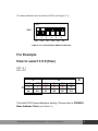
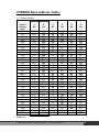
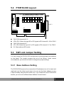
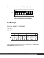
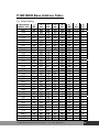
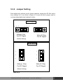
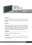
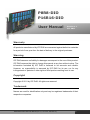
P8R8-DIO P16R16-DIO User Manual Version 1.7 Oct. 2011 Warranty All products manufactured by ICP DAS are warranted against defective materials for a period of one year from the date of delivery to the original purchaser. Warning ICP DAS assumes no liability for damages consequent to the use of this product. ICP DAS reserves the right to change this manual at any time without notice. The information furnished by ICP DAS is believed to be accurate and reliable. However, no responsibility is assumed by ICP DAS for its use, nor for any infringements of patents or other rights of third parties resulting from its use. Copyright Copyright © 2011 by ICP DAS. All rights are reserved. Trademark Names are used for identification only and may be registered trademarks of their respective companies. P8R8-DIO/P16R16-DIO User Manual (Ver.1.7, Oct. 2011, IMH-009-17) 1 Tables of Contents 1. INTRODUCTION ............................................................................................................................... 4 1.1 FEATURES AND APPLICATIONS ................................................................................................ 4 1.1.1 Features .................................................................................................................................. 4 1.1.2 Applications ....................................................................................................................... 4 1.2 PRODUCT CHECK LIST ............................................................................................................. 5 1.3 P8R8-DIO SPECIFICATIONS .................................................................................................... 6 2. P8R8-DIO INSTALLATION ............................................................................................................ 7 2.1 UNPACKING ............................................................................................................................. 7 2.2 P8R8-DIO LAYOUT ................................................................................................................ 8 2.3 SW1 AND JUMPER SETTING..................................................................................................... 8 2.3.1 Base Address Setting.......................................................................................................... 8 2.3.2 Jumper Setting ................................................................................................................. 11 2.4 PIN ASSIGNMENTS ................................................................................................................. 12 3. P8R8-DIO PROGRAMMING ........................................................................................................ 13 3.1 I/O ADDRESS MAP ................................................................................................................ 13 3.2 RELAY OUTPUT ..................................................................................................................... 14 3.2.1 Output Register ..................................................................................................................... 14 3.2.2 3.3 3.3.1 Using Relay Output ......................................................................................................... 15 ISOLATED INPUT .................................................................................................................... 16 Input Register .................................................................................................................. 16 3.3.2 Using Isolated Input............................................................................................................ 17 4. P16R16-DIO SPECIFICATIONS ................................................................................................... 18 5. P16R16-DIO INSTALLATION ...................................................................................................... 19 5.1 UNPACKING ........................................................................................................................... 19 5.2 P16R16-DIO LAYOUT .......................................................................................................... 20 5.3 SW1 AND JUMPER SETTING................................................................................................... 20 5.3.1 Base Address Setting........................................................................................................ 20 5.3.2 Jumper Setting ................................................................................................................. 24 5.4 PIN ASSIGNMENTS ................................................................................................................. 26 6. P16R16-DIO PROGRAMMING .................................................................................................... 28 6.1 I/O ADDRESS MAP ................................................................................................................ 28 6.2 RELAY OUTPUT ..................................................................................................................... 29 P8R8-DIO/P16R16-DIO User Manual (Ver.1.7, Oct. 2011, IMH-009-17) 2 6.2.1 Output Register................................................................................................................ 29 6.2.2 Using Relay Output............................................................................................................. 30 6.3 ISOLATED INPUT .................................................................................................................... 31 6.3.1 Input Register .................................................................................................................. 31 6.3.2 Using Isolated Input............................................................................................................ 32 7. TROUBLESHOOTING................................................................................................................... 33 7.1 8. PROBLEM ISOLATED .............................................................................................................. 33 SOFTWARE/HARDWARE INSTALLATION ....................................................................... 34 8.1 SOFTWARE INSTALLING PROCEDURE ........................................................................................... 34 8.2 HARDWARE INSTALLING PROCEDURE .......................................................................................... 35 P8R8-DIO/P16R16-DIO User Manual (Ver.1.7, Oct. 2011, IMH-009-17) 3 1. Introduction The P8R8-DIO/P16R16-DIO is an 8/16 isolated input and 8/16 relay output interface board designed for control and sensing applications. This interface board is easily installed in any PC/AT/XT or compatible computer. The P8R8-DIO/P16R16-DIO provides 8/16 electromechanical relay outputs and 8/16 optically isolated inputs. The P8R8-DIO/P16R16-DIO can be used in various applications including load switching, external switching, contact closure, etc. 1.1 Features and Applications 1.1.1 Features 8 relay outputs channels for P8R8-DIO 8 optically isolated inputs channels for P8R8-DIO 16 relay outputs channels for P16R16-DIO 16 optically isolated inputs channels for P16R16-DIO LED indicator for each relay output state AC/DC Signals Input AC Signal Input With Filter 1.1.2 Applications Factory Automation Laboratory Automation Security Control Product Test P8R8-DIO/P16R16-DIO User Manual (Ver.1.7, Oct. 2011, IMH-009-17) 4 1.2 Product Check List The shipping package includes the following items: One P8R8-DIO or P16R16-DIO series card One software utility ISA CD. One Quick Start Guide. It is recommended that you read the Quick Start Guide first. All the necessary and essential information is given in the Quick Start Guide, including: Where to get the software driver, demo programs and other resources. How to install the software. How to test the card. Attention! If any of these items is missing or damaged, contact the dealer from whom you purchased the product. Please save the shipping materials and carton in case you need to ship or store the product in the future. P8R8-DIO/P16R16-DIO User Manual (Ver.1.7, Oct. 2011, IMH-009-17) 5 1.3 P8R8-DIO Specifications Model Name P8R8-DIO Digital Input Isolation Voltage 5000 Vrms Channels 8 Compatibility Non-polarized OPTO-isolated Input Voltage Logic 0: 0 ~ 1 VAC/VDC Logic 1: 5 ~ 24 VAC/VDC Input Impedance 1.2 KΩ, 0.5 W Response Speed Without Filter: 0.045 MHz With Filter: 0.05 kHz Relay Output Relay Type 4 SPDT 4 SPST Channels 8 Contact Rating 0.3 A @ 120 VAC/ VDC 1 A @ 30 VDC Operating Time 5 ms (typical) Release Time 5 ms (typical) Insulation Resistance 100 MΩ Life Mechanical: 100,000 ops. (min.) Electrical: 100,000 at 1 A @ 30 V, resistive General Environmental I/O Connector Female DB37 x 1 Dimensions (L x W x D) 150 mm x 97 mm x 22 mm Power Consumption 160 mA @ +5 V (max.) 150 mA @ +12 V (max.) Operating Temperature 0 ~ 60 °C Storage Temperature -20 ~ 70 °C Humidity 5 ~ 85% RH, non-condensing P8R8-DIO/P16R16-DIO User Manual (Ver.1.7, Oct. 2011, IMH-009-17) 6 2. P8R8-DIO Installation This chapter describes the P8R8-DIO unpacking information; P8R8-DIO layout and the jumpers and switches settings for the P8R8-DIO configuration. 2.1 Unpacking CAUTION: Your P8R8-DIO card contains sensitive electronic components that can be easily damaged by static electricity. 1. The P8R8-DIO should be done on a grounded anti-static mat. 2. The user should wear an anti-static wristband, grounded at the same point as the anti-static mat. 3. Inspect the carton for obvious damage. Shipping and handing may cause damage to the board. Be sure there are no shipping and handling damages on the board before using. 4. After opening the carton, exact the system board and place it on a grounded anti-static surface and component side up. CAUTION: Do not apply power to the board if it has been damaged! 5. You are now ready to install your P8R8-DIO. P8R8-DIO/P16R16-DIO User Manual (Ver.1.7, Oct. 2011, IMH-009-17) 7 2.2 P8R8-DIO Layout LED CN 1 SW1 JP1-JP8 P8R8DIO CN1: DIO channels 0~7 JP1~JP8: Select the input AC or DC signals of D/I channel 0~7 SW1: Base address DIP switch 2.3 SW1 and Jumper Setting You can change the P8R8-DIO configuration by setting jumper and switches on the board. The board‘s jumpers are set at the factory. Under normal circumstances, you should not need to change the jumper settings. 2.3.1 Base Address Setting The P8R8-DIO requires two consecutive I/O addresses, one for output and read back and the other for input. You can set the base address on any 4-byte boundary using the DIP switch (SW1). If you install one more P8R8-DIO boards, you must set a different base address for each board. P8R8-DIO/P16R16-DIO User Manual (Ver.1.7, Oct. 2011, IMH-009-17) 8 The base address switch is preset at 300H (see Figure 2-1). ON SW1 1 2 3 A9 A8 A7 4 5 A6 6 A5 A4 Figure 2-1: Default Base Address 300 Hex For Example How to select 3 0 0 (Hex) OFF Æ 1 ON Æ 0 3 0 0 OFF OFF ON ON ON ON 1 1 0 0 0 0 1 A9 2 A8 3 A7 4 A6 5 A5 6 A4 The detail SW1 base addresses setting. Please refer to P8R8DIO Base Address Table (see Table 2-1). P8R8-DIO/P16R16-DIO User Manual (Ver.1.7, Oct. 2011, IMH-009-17) 9 P8R8DIO Base Address Table: (*): Default Setting SW1 Dip Switch Address (Hex) 1 A9 2 A8 3 A7 4 A6 5 A5 6 A4 200 210 220 230 240 250 260 270 280 290 2A0 2B0 2C0 2D0 2E0 2F0 OFF ON ON ON ON ON OFF ON ON ON ON OFF OFF ON ON ON OFF ON OFF ON ON ON OFF OFF OFF ON ON OFF ON ON OFF ON ON OFF ON OFF OFF ON ON OFF OFF ON OFF ON ON OFF OFF OFF OFF ON OFF ON ON ON OFF ON OFF ON ON OFF OFF ON OFF ON OFF ON OFF ON OFF ON OFF OFF OFF ON OFF OFF ON ON OFF ON OFF OFF ON OFF OFF ON OFF OFF OFF ON OFF ON OFF OFF OFF OFF 300 (*) 310 320 330 340 350 360 370 380 390 3A0 3B0 3C0 3D0 3E0 3F0 OFF OFF ON ON ON ON OFF OFF ON ON ON OFF OFF OFF ON ON OFF ON OFF OFF ON ON OFF OFF OFF OFF ON OFF ON ON OFF OFF ON OFF ON OFF OFF OFF ON OFF OFF ON OFF OFF ON OFF OFF OFF OFF OFF OFF ON ON ON OFF OFF OFF ON ON OFF OFF OFF OFF ON OFF ON OFF OFF OFF ON OFF OFF OFF OFF OFF OFF ON ON OFF OFF OFF OFF ON OFF OFF OFF OFF OFF OFF ON OFF OFF OFF OFF OFF OFF Table 2-1 P8R8-DIO/P16R16-DIO User Manual (Ver.1.7, Oct. 2011, IMH-009-17) 10 2.3.2 Jumper Setting Each digital input channel can be jumper selected, single-pole, RC filter with a time constant of 1.2 ms. Refer to the table 2-2 to see the list of jumper number and it’s corresponding digital input channel. JP 1 ~ JP 8 1 2 3 1 Without Filter For DC Signal 2 3 With AC Filter For AC Signal (Default Setting) Jumper Input Channels JP1 DI 0 JP2 DI 1 JP3 DI 2 JP4 DI 3 JP5 DI 4 JP6 DI 5 JP7 DI 6 JP8 DI 7 Table 2-2. If you are using AC input signals, you must short the AC FILTER jumper 1-2. If you are using DC input signals, the AC FILTER is optional. If the DC input signals response less than 20 μs, set the filter off. If you want a slow response (about 5 ~ 10 ms) for rejecting noise or contact bouncing, short the AC FILTER jumper 1-2.7 P8R8-DIO/P16R16-DIO User Manual (Ver.1.7, Oct. 2011, IMH-009-17) 11 2.4 Pin Assignments Figure 2-3: CN 1 pin assignments of the P8R8DIO connector. C ON1 NO 0 CO M 0 NC 0 NO 1 COM 1 NC 1 NO 2 COM 2 NC 2 NO 7 CO M 7 DI 0+ D I 1+ D I 2+ D I 3+ D I 4+ D I 5+ D I 6+ D I 7+ 1 2 3 4 5 6 7 8 9 10 11 12 13 14 15 16 17 18 19 20 21 22 23 24 25 26 27 28 29 30 31 32 33 34 35 36 37 NO 3 C OM NC 3 NO 4 C OM NO 5 CO M NO 6 CO M GN D DI 0DI 1DI 2DI 3DI 4DI 5D I 6D I 7- 3 4 5 6 NO n : Normally open. COM n : Common. NC n : Normally close. DI n : Digital input channel n. P8R8-DIO/P16R16-DIO User Manual (Ver.1.7, Oct. 2011, IMH-009-17) 12 3. P8R8-DIO Programming This chapter provides the I/O map of P8R8-DIO registers. Example programs and programming information are also included. 3.1 I/O Address Map The P8R8DIO boards occupy two consecutive addresses in the computer’s I/O space. The base address is selected by DIP switch. The I/O map is shown in Table 3-1. Base Address at 300 Hex Address Write Read Base + 0 Relay Output (CH 0 ~ CH 7) Read Back The Output Status Base + 1 NO FUNCTION DIGITAL INPUT (CH0 ~ CH7) Table 3-1. I/O Address Map. P8R8-DIO/P16R16-DIO User Manual (Ver.1.7, Oct. 2011, IMH-009-17) 13 3.2 Relay Output You write data to relays (CH0 - CH 7 ) as a single Byte. Each of the eight bits within a byte controls a single relay. A high bit (equal to1) energizes (closes the contacts of) a relay while a low bit (equal to 0) turns the relay off. 3.2.1 Output Register Relay Output register bits are assigned as shown in Table 3-2 Base Address at 300 Hex Base+0 D7 D6 D5 D4 D3 D2 D1 D0 Output Channel 7 6 5 4 3 2 1 0 Table 3-2. Relay Addresses in the Relay Output Register. For Example (Basic Language) REM : Set all relay output is ON , ( Output data FFh) Base=&h300 ‘ Set Base Address at 300 (Hex) Out Base , &hFF ‘ Set Relay Output (Ch 0 ~ Ch 7) On RB= Inp(Base) ‘ Read Back Relay Output Ch 0 ~ Ch 7 REM: Set relay output CH 3 is ON, Output data 8h (00001000 BIN) Out Base, &h8 ‘ Set relay output CH 3 ON (For C Language) outportb(0x300,0x0FF); /* Set all relay output is On*/ outportb(0x300,0x0); /* Set all relay output is Off*/ P8R8-DIO/P16R16-DIO User Manual (Ver.1.7, Oct. 2011, IMH-009-17) 14 3.2.2 Using Relay Output Basic Circuitry : (Current Rating < 0.3 A ), Refer to Fig. 3-1. P8R8DIO Relay COM NO Load AC/ DC Power Supply Figure 3-1. Heavy Loading Application ( > 0.3 A ), Refer to Figure.3-2. P8R8DIO Relay AC/ DC Power Supply Power Relay Contact Power Relay Heavy Loading Figure 3-2. P8R8-DIO/P16R16-DIO User Manual (Ver.1.7, Oct. 2011, IMH-009-17) 15 3.3 Isolated Input The digital input state is read as a single byte from the port at base address+1. Each of the eight bits within the byte corresponds to a particular digital input so that a high bit (equal to 1) represents a high state while a low bit (equal to 0) represents a low state. Register bits are assigned as shown in Table 3-3. 3.3.1 Input Register Base Address at 300 Hex Base + 1 D7 D6 D5 D4 D3 D2 D1 D0 Input Channel 7 6 5 4 3 2 1 0 Table 3-3 input addresses in the isolated control input Register. For Example (Basic Language) Base=&h300 ‘ Set Base Address at 300 (Hex) RIH=INP(Base+1) ‘ Read Isolated Input Ch 0 ~ Ch 7 ( C Language ) int rih; rih=inportb(0x301); P8R8-DIO/P16R16-DIO User Manual (Ver.1.7, Oct. 2011, IMH-009-17) 16 3.3.2 Using Isolated Input Basic Circuit Switch DI n + If Using AC Signal, the P8R8DIO JP1 must be shorted 1-2, refer to Chapter 2-3-2 5 ~ 24 VAC/VDC DI n Figure 3-3. n is the channel number The normal input voltage range is 5 ~ 24 VAC or VDC. The normal input range can be changed by choosing suitable resistor to limit the current through the opto-isolator to about 10 mA( If ). The default resistor is 1.2 kΩ / 0.5 W. Ri = 1.2 kΩ /0.5 W VIN 24 V If = 10 mA PC - 814 Figure 3-4. Ri = Vin / If Pw = Vin X If Calculation Example : If Vin = 120 V Then Ri = 120 (V) / 0.01 (A) = 12 kΩ Pw = 120 (V) X 0.01 (A) = 1.2 W The Ri Must Replace By 12 kΩ / 2 W (1.2 W) P8R8-DIO/P16R16-DIO User Manual (Ver.1.7, Oct. 2011, IMH-009-17) 17 4. P16R16-DIO Specifications Model Name P16R16-DIO Digital Input Isolation Voltage 5000 Vrms Channels 16 Compatibility Non-polarized OPTO-isolated Input-Voltage Logic 0: 0 ~ 1 VAC/VDC Logic 1: 5 ~ 24 VAC/VDC Input Impedance 1.2 KΩ, 0.5 W Response Speed Without Filter: 0.045 MHz With Filter: 0.05 kHz Relay Output Relay Type 8 SPDT 8 SPST Relay Output Channels 16 Contact Rating 0.3 A @ 120 VAC/VDC 1 A @ 30 VDC Operating Time 5 ms (typical) Release Time 5 ms (typical) Insulation Resistance 100 MΩ Mechanical: 100,000 ops. (min.) Electrical: 100,000 at 1 A @ 30 V, resistive Life General Environmental I/O Connector Female DB37 x 1 Dimensions (L x W x D) 175 mm x 121 mm x 22mm Power Consumption 200 mA @ +5 V (max.) 260 mA @ +12 V (max.) Operating Temperature 0 ~ 60 °C Storage Temperature -20 ~ 70 °C Humidity 5 ~ 85% RH, non-condensing 5. P16R16-DIO Installation This chapter describes the P16R16-DIO unpacking information; P16R16-DIO layout and the jumpers and switches settings for the P16R16-DIO configuration. 5.1 Unpacking CAUTION: Your P16R16-DIO card contains sensitive electronic components that can be easily damaged by static electricity. 6. The P16R16-DIO should be done on a grounded anti-static mat. 7. The user should wear an anti-static wristband, grounded at the same point as the anti-static mat. 8. Inspect the carton for obvious damage. Shipping and handing may cause damage to the board. Be sure there are no shipping and handling damages on the board before using. 9. After opening the carton, exact the system board and place it on a grounded anti-static surface & component side up. CAUTION: Do not apply power to the board if it has been damaged! 10. You are now ready to install your P16R16-DIO. P8R8-DIO/P16R16-DIO User Manual (Ver.1.7, Oct. 2011, IMH-009-17) 19 5.2 P16R16-DIO Layout LED 8 9 10 11 12 13 14 15 7 6 5 4 3 2 1 0 CON 2 CN1 S1 JP9-JP16 JP1-JP8 CN1: DIO channels 8~16 JP8~JP16: Select the input AC or DC signals of D/I channel 8~16 for CON 1 CN2: DIO channels 0~7 JP1~JP8: Select the input AC or DC signals of D/I channel 0~7 for CON 2 S1: Base address DIP switch 5.3 SW1 and Jumper Setting You can change the P16R16-DIO configuration by setting jumper and switches on the board. The board‘s jumpers are set at the factory. Under normal circumstances, you should not need to change the jumper settings. 5.3.1 Base Address Setting The P16R16-DIO requires four consecutive I/O addresses, two is for output and read back and the other‘s is for input. You can set the base address on any 4-byte boundary using the DIP switch (S1). If you install one more P16R16-DIO boards, you must set a different base address for each board. P8R8-DIO/P16R16-DIO User Manual (Ver.1.7, Oct. 2011, IMH-009-17) 20 The base address switch is preset at 300H (see Figure 2-1). ON SW1 1 2 3 4 5 6 7 8 A3 A4 A5 A6 A7 A8 A9 X Figure 2-1: Default Base Address 300 Hex For Example How to select 3 0 0 (Hex) OFF Æ 1 ON Æ 0 3 0 0 OFF OFF ON ON ON ON ON 1 1 0 0 0 0 0 7 A9 6 A8 5 A7 4 A6 3 A5 2 A4 1 A3 The detail SW1 base addresses setting. Please refer to P16R16-DIO Base Address Table (see Table 2-1). P8R8-DIO/P16R16-DIO User Manual (Ver.1.7, Oct. 2011, IMH-009-17) 21 P16R16DIO Base Address Table: (*): Default Setting S1 Dip Switch Address (Hex) 1 A3 2 A4 3 A5 4 A6 5 A7 6 A8 7 A9 8 X 200 208 210 218 220 228 230 238 240 248 250 258 260 268 270 278 280 288 290 298 2A0 2A8 2B0 2B8 2C0 2C8 2D0 2D8 2E0 2E8 2F0 2F8 ON ON ON ON ON ON OFF X OFF ON ON ON ON ON OFF X ON OFF ON ON ON ON OFF X OFF OFF ON ON ON ON OFF X ON ON OFF ON ON ON OFF X OFF ON OFF ON ON ON OFF X ON OFF OFF ON ON ON OFF X OFF OFF OFF ON ON ON OFF X ON ON ON OFF ON ON OFF X OFF ON ON OFF ON ON OFF X ON OFF ON OFF ON ON OFF X OFF OFF ON OFF ON ON OFF X ON ON OFF OFF ON ON OFF X OFF ON OFF OFF ON ON OFF X ON OFF OFF OFF ON ON OFF X OFF OFF OFF OFF ON ON OFF X ON ON ON ON OFF ON OFF X OFF ON ON ON OFF ON OFF X ON OFF ON ON OFF ON OFF X OFF OFF ON ON OFF ON OFF X ON ON OFF ON OFF ON OFF X OFF ON OFF ON OFF ON OFF X ON OFF OFF ON OFF ON OFF X OFF OFF OFF ON OFF ON OFF X ON ON ON OFF OFF ON OFF X OFF ON ON OFF OFF ON OFF X ON OFF ON OFF OFF ON OFF X OFF OFF ON OFF OFF ON OFF X ON ON OFF OFF OFF ON OFF X OFF ON OFF OFF OFF ON OFF X ON OFF OFF OFF OFF ON OFF X OFF OFF OFF OFF OFF ON OFF X ON ON ON ON ON OFF OFF X OFF ON ON ON ON OFF OFF X ON OFF ON ON ON OFF OFF X 300(*) 308 310 P8R8-DIO/P16R16-DIO User Manual (Ver.1.7, Oct. 2011, IMH-009-17) 22 318 320 328 330 338 340 348 350 358 360 368 370 378 380 388 390 398 3A0 3A8 3B0 3B8 3C0 3C8 3D0 3D8 3E0 3E8 3F0 3F8 OFF OFF ON ON ON OFF OFF X ON ON OFF ON ON OFF OFF X OFF ON OFF ON ON OFF OFF X ON OFF OFF ON ON OFF OFF X OFF OFF OFF ON ON OFF OFF X ON ON ON OFF ON OFF OFF X OFF ON ON OFF ON OFF OFF X ON OFF ON OFF ON OFF OFF X OFF OFF ON OFF ON OFF OFF X ON ON OFF OFF ON OFF OFF X OFF ON OFF OFF ON OFF OFF X ON OFF OFF OFF ON OFF OFF X OFF OFF OFF OFF ON OFF OFF X ON ON ON ON OFF OFF OFF X OFF ON ON ON OFF OFF OFF X ON OFF ON ON OFF OFF OFF X OFF OFF ON ON OFF OFF OFF X ON ON OFF ON OFF OFF OFF X OFF ON OFF ON OFF OFF OFF X ON OFF OFF ON OFF OFF OFF X OFF OFF OFF ON OFF OFF OFF X ON ON ON OFF OFF OFF OFF X OFF ON ON OFF OFF OFF OFF X ON OFF ON OFF OFF OFF OFF X OFF OFF ON OFF OFF OFF OFF X ON ON OFF OFF OFF OFF OFF X OFF ON OFF OFF OFF OFF OFF X ON OFF OFF OFF OFF OFF OFF X OFF OFF OFF OFF OFF OFF OFF X Table 2-1 P8R8-DIO/P16R16-DIO User Manual (Ver.1.7, Oct. 2011, IMH-009-17) 23 5.3.2 Jumper Setting Each digital input channel can be jumper selected, single-pole, RC filter with a time constant of 1.2 ms. Refer to Figure 2-2 to see the lost of jumper and it’s corresponding digital input channel number. JP 1 ~ JP 8 1 2 3 1 2 3 Without Filter For DC Signal With AC Filter For AC Signal (Default Setting) JP 9 ~ JP 16 3 3 2 2 1 1 Without Filter For DC Signal With AC Filter For AC Signal (Default Setting) Figure 2-2 P8R8-DIO/P16R16-DIO User Manual (Ver.1.7, Oct. 2011, IMH-009-17) 24 Jumper Input Channels Jumper Input Channels JP1 DI 0 JP9 DI 8 JP2 DI 1 JP10 DI 9 JP3 DI 2 JP11 DI 10 JP4 DI 3 JP12 DI 11 JP5 DI 4 JP13 DI 12 JP6 DI 5 JP14 DI 13 JP7 DI 6 JP15 DI 14 JP8 DI 7 JP16 DI 15 Table 2-2. If you are using AC input signals, you must short the AC FILTER jumper 1-2. If you are using DC input signals, the AC FILTER is optional. If the DC input signals response less than 20 μs, set the filter off. If you want a slow response (about 5 ~ 10 ms) for rejecting noise or contact bouncing short the AC FILTER jumper 1-2. P8R8-DIO/P16R16-DIO User Manual (Ver.1.7, Oct. 2011, IMH-009-17) 25 5.4 Pin Assignments CON1 CON2 Extender Cable NO n COM n NC n DI n P8R8-DIO/P16R16-DIO User Manual (Ver.1.7, Oct. 2011, IMH-009-17) : Normally Open. : common. : Normally closed. : Digital input channel n. 26 NC: Normally Closed COM: Common NO: Normally Open Figure 3-4. SPDT RELAY: Single Pole Double Throw. DI n +: Digital Input Jumper AC Filter DI n -: Digital Input PC - Figure 3-5. Isolated Input. P8R8-DIO/P16R16-DIO User Manual (Ver.1.7, Oct. 2011, IMH-009-17) 27 6. P16R16-DIO Programming This chapter provides the I/O map of P16R16-DIO registers. Example programs and programming information are also included. 6.1 I/O Address Map The P16R16DIO boards occupy four consecutive addresses in the computer’s I/O space. The base address is selected by DIP switch, The I/O map are shown in Table 3-1. P16R16DIO Base Address at 300 Hex Address Write Read Base + 0 Relay Output (CH 0 ~ CH 7) Read Back The Output Status Base + 1 Relay Output (CH 8 ~ CH15) Read Back The Output Status Base + 2 No Function Digital Input (CH0~CH7) Base + 3 No Function Digital Input (CH8~CH18) Table 3-1. P16R16DIO I/O Address Map. P8R8-DIO/P16R16-DIO User Manual (Ver.1.7, Oct. 2011, IMH-009-17) 28 6.2 Relay Output You write data to relays as a single Byte. Each of the eight bits within a byte controls a single relay. A high bit (equal to1) energizes (closes the contacts of) a relay while a low bit (equal to 0) turns the relay off. 6.2.1 Output Register Relay Output register bits are assigned as shown in Table 3-2. P16R16DIO Base Address at 300 Hex Base+0 D7 D6 D5 D4 D3 D2 D1 D0 Output Channel 7 6 5 4 3 2 1 0 Base+1 D7 D6 D5 D4 D3 D2 D1 D0 Output Channel 15 14 13 12 11 10 9 8 Table 3-2 P16R16DIO Relay Addresses in the Relay Output Register. Base+0 D7 D6 D5 D4 D3 D2 D1 D0 Read back channel 7 6 5 4 3 2 1 0 Base+1 D7 D6 D5 D4 D3 D2 D1 D0 Read back channel 15 14 13 12 11 10 9 8 Table 3-3. Relay output read back register. For Example (Basic Language) REM: Set all relay output is ON , ( Output data FFh) Base=&h300 Out Base , &hFF ‘ Set Base Address at 300 (Hex) ‘ Set Relay Output (Ch 0 ~ Ch 7) On Out Base +1, &hFF ‘ Set Relay Output (Ch 8 ~ Ch 15) On RBL= Inp(Base) ‘ Read Back Relay Output Ch 0 ~ Ch 7 RBH= Inp(Base+1) ‘ Read Back Relay Output Ch 8 ~ Ch 15 REM : Set relay output CH 3 is ON ,Output data 8h (00001000 BIN) Out Base,&h8 ‘ Set relay output CN2 D3 ON P8R8-DIO/P16R16-DIO User Manual (Ver.1.7, Oct. 2011, IMH-009-17) 29 6.2.2 Using Relay Output Basic Circuitry: (Current Rating < 0.3 A), Refer to Figure 3-1. P8R8DIO Relay COM NO Load AC/ DC Power Supply Figure 3-1. Heavy Loading Application (>0.3 A). Refer to Figure 3-2. P8R8DIO Relay AC/ DC Power Supply Power Relay Contact Power Relay Heavy Loading Figure 3-2. P8R8-DIO/P16R16-DIO User Manual (Ver.1.7, Oct. 2011, IMH-009-17) 30 6.3 Isolated Input The digital input state are read as a single byte from the port at base address+1 . Each of the eight bits within the byte corresponds to a particular digital input so that a high bit (equal to 1 ) represent a high state while a low bit (equal to 0) represent a low state . Register bits are assigned as shown in Table 3-3 6.3.1 Input Register Base Address at 300 Hex Base + 1 D7 D6 D5 D4 D3 D2 D1 D0 Input Channel 7 6 5 4 3 2 1 0 Table 3-3. input addresses in the isolated control input Register. For Example (Basic Language) Base=&h300 ‘ Set Base Address at 300 (Hex) RIH=Inp(Base+1) ‘ Read Isolated Input Ch 0 ~ Ch 7 P8R8-DIO/P16R16-DIO User Manual (Ver.1.7, Oct. 2011, IMH-009-17) 31 6.3.2 Using Isolated Input Basic Circuit Switch DI n + If Using AC Signal, the P16R16DIO JP1 must be shorted 1-2, ref. to chapter 2-3-2 5 ~ 24 VAC/ VDC DI n Figure 3-3, n is the channel number. The normal input voltage range is 5 ~ 24 VAC or VDC. The normal input range can be changed by choosing suitable resistor to limit the current through the opto-isolator to about 10 mA( If ). The default resistor is 1.2 kΩ / 0.5 W. Ri = 1.2 kΩ / 0.5 W VIN 24 V If = 10 mA Figure 3-4. PC - 814 Ri = Vin / If Pw = Vin X If Calculation Example: If Vin = 120 V Then Ri = 120 (V) / 0.01 (A) = 12 kΩ Pw = 120 (V) X 0.01 (A) = 1.2 W The Ri Must Replace By 12 kΩ / 2 W (1.2 W) P8R8-DIO/P16R16-DIO User Manual (Ver.1.7, Oct. 2011, IMH-009-17) 32 7. Troubleshooting If your P8R8DIO board is not operating properly, use the information in this chapter to isolate the problem. 7.1 Problem Isolated You can use an ohmmeter to check operation of the relay outputs and a low voltage power supply to check the isolated inputs. You can use DOS DEBUG program to exercise relay outputs or read the input ports, or you can use the INP and OUT commands of the BASIC language. For example, using DEBUG for a P8R8-DIO at a base address set to &H300 is as follows: O O O 300 FF 300 0 300 08 ‘Turn On all Relays. ‘Turn Off all Relays. ‘Turn On Bit D3 Relay. I I 300 301 ‘Read back Relay status ‘Read Digital Input Data P8R8-DIO/P16R16-DIO User Manual (Ver.1.7, Oct. 2011, IMH-009-17) 33 8. Software/Hardware Installation The can be used in DOS and Windows 98/ME/NT/2K and 32-bit Windows XP/2003/Vista/7. The recommended installation procedure for windows is given in Sec. 8.1 ~8.2. Or refer to Quick Start Guide (CD:\NAPDOS\ISA\DIO\Manual\QuickStart\). http://ftp.icpdas.com/pub/cd/iocard/isa/napdos/isa/dio/manual/quickstart/ 8.1 Software Installing Procedure P8R8DIO/P16R16DIO Windows driver (Windows 98/NT/2K and 32-bit Windows XP/2003/ Vista/7): Step 1: Insert the companion CD into the CD-ROM drive and after a few seconds the installation program should start automatically. If it doesn’t start automatically for some reason, double-click the AUTO32.EXE file in the NAPDOS folder on this CD. Step 2: Click the item: “Install Toolkits (Softwares)/Manuals”. Step 3: Click the item: “ISA Bus DAQ Card”. Step 4: Click the item: “DIO”. Step 5: Choose the “Install Toolkit for Windows 95/98、NT or 2000” for setup according to your PC platform and then install driver. Notes: 1. The P8R8DIO/P16R16DIO Windows driver site location: http://ftp.icpdas.com/pub/cd/iocard/isa/napdos/isa/dio/dll/ 2. The Windows 2000 (Win2K) driver support Windows 2000 and 32-bit Windows XP/2003/Vista/7. P8R8-DIO/P16R16-DIO User Manual (Ver.1.7, Oct. 2011, IMH-009-17) 34 Step 6: Step 7: Step 8: Step 9: Click “Next>” button to start installation. Click “Next>” button to install driver into the default folder. Click “Next>” button to continue installation. Select “No, I will restart my computer late” and then click “Finish” button. 8.2 Hardware Installing Procedure Please set the base address on the P8R8DIO/P16R16DIO card before insert P8R8DIO/P16R16DIO card into the ISA slot in the computer. For detailed base address information refer to Section 2.3.1 “P8R8DIO Base Address Setting” and 5.3.1 “P16R16DIO Base Address Setting”. For example: base address is 0x300. Step 1: Step 2: Step 3: Step 4: Step 5: Step 6: Shout down and power off your computer. Remove all covers from the computer. Select an empty ISA slot. Care fully insert your P8R8DIO/P16R16DIO card into the ISA slot. Replace the PC covers. Power on the computer. P8R8-DIO/P16R16-DIO User Manual (Ver.1.7, Oct. 2011, IMH-009-17) 35 Adding Hardware Notes: adding hardware for working on Windows 2000 and 32-bit Windows XP/2003/Vista/7 only. Windows 95/98/Me/NT users should install correct version of the driver on the CD-ROM, and skip these “Adding Hardware” procedures. Step 7: Open the “Control Panel” by click the item “Start >> Settings >> Control Panel ”. Step 8: Double-click the item “Add Hardware” and click the “Next>” button. Step 9: Select the item “Yes, I have already connected the hardware” and click the “Next>” button. Step 10: Selection the item “Add a new hardware device” and click the “Next>” button. Step 11: Selection the item “Install the hardware that I manually select from a list [Advanced]” and click the “Next>” button. Step 12: Selection the item “Show All Devices” and click the “Next>” button. Step 13: Click the “Have Disk...” button. Step 14: Click the “Browse...” button to select the .Inf file default path is C:\DAQPRO\DIO_Win2K\Inf and click the “Open” and “OK” button. P8R8-DIO/P16R16-DIO User Manual (Ver.1.7, Oct. 2011, IMH-009-17) 36 Step 15: Selection then correct device from the “Models:” listbox and click the “Next>” button. Step 16: Click the “Next>” button and then click the “Finish” button. Modify the device properties Step 17: Double-click the “System” icon in the “Control Panel”. Step 18: Click the “Hardware” tab and then click the “Device Manager” button. Step 19: Click the “DAQCard” tab and then double-click “ICPDAS P16R16-DIO Digital I/O Card” (or ICPDAS P8R8-DIO Digital I/O Card). Step 20: Select the “Resources” tab and then setting as follows: 4. Change to base address set by SW1 1. Select I/O Range 5. Check the Conflict information 2. Uncheck 3. Click Complete P8R8-DIO/P16R16-DIO User Manual (Ver.1.7, Oct. 2011, IMH-009-17) 37