1
Decision Guide and Development Process
Coherent Accelerator Processor Interface (CAPI) for POWER8 Systems
2.3
Physical Considerations
There are two key questions to answer to decide if your algorithm will work on the CAPI Developer Kit
FPGA from a physical standpoint.
Will your algorithm fit on the Developer Kit FPGA?
The IBM-supplied power service layer (PSL) co-resides on the FPGA with your acceleration engine. The
PSL handles communications, address translation, and caching of data for the accelerator to work with
the POWER8 core. The PSL comes as a preplaced entity on the FPGA and runs at 250 MHz. The PSL
uses just under 25% of the Stratix V FPGA’s adaptive look-up tables (ALUTs), arrays, and digital signal
processors (DSPs). For the complete device specifications, see
http://www.altera.com/devices/fpga/stratix-fpgas/stratix-v/stxv-index.jsp .
For estimation purposes, plan on your algorithm fitting in 70% of the overall ALUTs, arrays, and DSPs.
Table 1 shows the maximum remaining resources available for the accelerator functional unit (AFU) after
placing the PSL.
Table 1: FPGA Resources Available for the AFU
Item
Total Available for AFU
ALUTs
M20K memory blocks
DSP
341,548
1874
188
Does the Developer Kit Card have the necessary I/Os?
If your algorithm requires I/O resources in addition to logic blocks on the FPGA, see the specifications for
the CAPI Developer Kit card (http://www.nallatech.com/PCI-Express-FPGA-Cards/pcie-385n-alterastratix-v-fpga-computing-card.html). Generally, the card has DRAM and SFP+ 10 Gb connectors.
If either of these answers indicates that the CAPI Developer Kit will not work, you might still have options
if you can use the SFP+ connectors on the card to split your algorithm to an external engine. In this case,
the FPGA on the CAPI Developer Kit card contains logic for interfacing to the application through the PSL
and can contain some of your accelerator engine. The rest of the accelerator engine resides off card on
your own custom board, using the SFP+ high-speed connection to communicate between them.
3 CAPI Developer Kit Process
Best practices for creating a CAPI solution dictate using the rigorous development process outlined in this
section. The CAPI User’s Manual has additional details. After deciding to move forward with creating a
CAPI solution, plan on two phases: a high-level design (HLD) phase and an implementation phase.
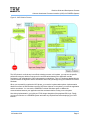
Figure 2 on page 8Figure 2: CAPI Solution Process shows the entire process in flowchart form.
20 October 2014
Page 7