1
US006389558B1
(12) United States Patent
(10) Patent N0.:
(45) Date of Patent:
Herrmann et al.
(54)
EMBEDDED LOGIC ANALYZER FOR A
PROGRAMMABLE LOGIC DEVICE
(75)
Inventors:
FOREIGN PATENT DOCUMENTS
Alan L. Herrmann, Sunnyvale; Greg
Notice:
2/1992
OTHER PUBLICATIONS
Joshua MarantZ, “Enhanced visibility and performance in
functional veri?cation by reconstruction”, Proceedings of
(US)
(*)
4042262
DE
P. Nugent, Menlo Park, both of CA
(73) Assignee:
US 6,389,558 B1
*May 14, 2002
the 35* annual conference on Design automation confer
Altera Corporation, San Jose, CA
(US)
ence, p. 164—169.
Charles Stroud et al. “Evaulation of FPGA resources for
Subject to any disclaimer, the term of this
patent is extended or adjusted under 35
built—in self—test of programmable logic blocks”, Proceed
U.S.C. 154(b) by 0 days.
ings of the 1996 ACM fourth international symposium on
?eld—programmable gate arrays, p. 107.
(List continued on neXt page.)
This patent is subject to a terminal dis
claimer.
Primary Examiner—Gilberto Barron, Jr.
Assistant Examiner—Christopher A. Revak
(74) Attorney, Agent, or Firm—Beyer Weaver & Thomas,
(21) Appl. No.: 09/610,787
Jul. 6, 2000
(22) Filed:
LLP
(57)
Related US. Application Data
ABSTRACT
A technique for embedding a logic analyZer in a program
mable logic device alloWs debugging of such a device in its
(63)
(60)
Continuation of application No. 08/958,435, ?led on Oct.
27, 1997, now Pat. No. 6,182,247.
Provisional application No. 60/029,277, ?led on Oct. 28,
1996.
embedded Within a PLD, it captures and stores logic signals,
and it unloads these signals through an interface to be
(51)
(52)
Int. Cl.7 ........................ .. G06F 17/50; G06F 11/25
vieWed on a computer. Using an electronic design automa
tion (EDA) softWare tool running on a computer system, an
actual operating conditions. A logic analyZer circuit is
US. Cl. ....................... .. 714/39; 714/725; 714/734;
engineer speci?es signals of the PLD to be monitored,
speci?es the number of samples to be stored, and speci?es
a system clock signal and a trigger condition that Will begin
the acquisition of data. The EDA tool then automatically
inserts the logic analyZer circuit into the electronic design of
702/117; 716/4
(58)
Field of Search ............................ .. 714/20, 31, 32,
714/25, 39, 45, 46, 724, 38, 725, 733, 734,
738; 702/58, 59, 81, 82, 84, 83, 117; 395/50005,
500.17; 716/4, 5, 6, 12, 16, 17, 14, 15;
703/17, 28; 717/5
the PLD Which is compiled and downloaded to con?gure the
PLD. Using an interface connected betWeen the PLD and the
computer, the EDA tool communicates With the embedded
logic analyZer in order to arm the circuit and to poll it until
an acquisition has been made. The EDA tool then directs the
References Cited
(56)
U.S. PATENT DOCUMENTS
4,696,004
4,788,492
4,835,736
4,847,612
5,036,473
5,058,114
A
A
A
A
A
A
9/1987
11/1988
5/1989
7/1989
7/1991
10/1991
logic analyZer to unload the data from its capture buffer and
then displays the data on the computer. The logic analyZer
Nakajima et al.
Schubert
circuit may then be rearmed to capture another sequence of
Easterday
Kaplinsky
sample values. The trigger condition may be changed With
out recompiling. The design may be recompiled With neW
Butts et al.
Kuboki et al.
logic analyZer parameters to debug a different portion.
27 Claims, 7 Drawing Sheets
(List continued on neXt page.)
f252
ELECTED/‘vac SYSTEM
PLD
f18
COMPUTER
SYSTEM
A
@254 ~76
USER
LOG/C
256f
W
262/11,
EMBEDDED
LOG/C
ANALYZER
266
264
70
L
260
US 6,389,558 B1
Page 2
2/2000 Patel et al.
12/2000 Zuveri et al.
1/2001 Herrmann et al.
..
6,247,147 B1 * 6/2001 Beenstra et al.
6,286,114 B1 * 9/2001 Veenstra et al. ............ ..
U.S. PATENT DOCUMENTS
5,124,588
5,329,470
5,365,165
5,425,036
5,452,231
5,568,437
5,572,712
5,629,617
5,640,542
5,661,662
5,717,695
5,717,699
5,764,079
5,821,771
5,870,410
5,960,191
6,014,334
6,016,563
>J
*
*
6/1992
7/1994
11/1994
6/1995
9/1995
10/1996
11/1996
5/1997
6/1997
8/1997
2/1998
2/1998
6/1998
10/1998
2/1999
9/1999
1/2000
1/2000
6,020,758 A
6,157,210 A
6,182,247 B1
Baltus et al.
Sample et al.
El-Ayat et al.
Lui et al.
Butts et al.
Jamal
Jamal
714/39
714/39
OTHER PUBLICATIONS
Robert R. Collins, “Overview of Pentium Probe Mode,”
(WWW.X86.org/articles/probemd/ProbeMode.htn), Aug. 21,
Uhling et al.
1998, 3 pages.
Robert R. Collins, “ICE Mode and the Pentium Processor,”
Whitsel et al.
Butts et al.
Manela et al.
(WWW.X86.org/ddj/Nov97/Nov97.htm), Aug. 21, 1998, 6
Haag et al.
pages.
Patel et al.
................. .. 326/40
Patel et al.
................. .. 326/38
Norman et al.
Sample et al.
Patel et al.
Fleisher
.......... ..
365/189.08
“Pentium® Pro Family Developer’s Manual,” vol. 1: Speci
?cations, Intel® Corporation, 1996, 9 pages.
Pentium® Processor User’s Manual, vol. 1, Intel Corpora
tion®, 1993, p. 11—3 .
* cited by examiner
U.S. Patent
May 14, 2002
US 6,389,558 B1
Sheet 1 0f 7
[7O
PROGRAMMABLE W76
LOG/C DEV/CE
{Ix/28 ~74
230 COMPUTER
SYSTEM
E/LE SERVER
PROGRAMMING
UN/ T
24\
k» 25
|
COMPUTER
SYSTEM
A
l
|
COMPUTER
SYSTEM
L15
$72
l
COMPUTER
SYSTEM
C
L22
f252
ELECTRON/C SYSTEM
"v76
PLD
r78
COMPUTER
SYSTEM
A
T72?
266
EMBEDDED
LOG/C
ANALYZER
l 260
70
FIG. 5
U.S. Patent
May 14, 2002
Sheet 2 0f 7
US 6,389,558 B1
BEGIN DESIGN OF
50
PROGRAMMABLE LOGIC
DEVICE
OBTAIN SYSTEM SPECIFICATION
/52
I
-——>
CREATE TOP LEVEL BLOCK DIAGRAM
/54
I
GENERATE DESIGN FILE TEMPLATES
[/56
I
P
D
IMPLEMENT BLOCK
/58
I
SIMULATE BLOCK
/60
I
<——
COMBINE BLOCKS
/62
I
<——-—
SIMULATE ENTIRE DESIGN
/64
I
COMPILE ENTIRE DESIGN
/ 56
I
(—
OPTIMIZE DESIGN PERFORMANCE
68
I
PROGRAM/CONFIGURE LOGIC DEVICE AND TEST IN SYSTEM
FIG. 2
/70
U.S. Patent
FIG. 3A
May 14, 2002
Sheet 3 0f 7
US 6,389,558 B1
100
BEGIN
/
EMBED LOGIC ANALYZER, CAPTURE AND
VIEW RESULTS
GENERATE DEVICE DESIGN AND COMPILE
/102
I
/104
PROGRAM DEVICE, PLACE DEVICE IN OPERATING CONDITIONS
AND OBSERVE MALFUNCTIONS
I
/106
ENABLE HARDWARE DEBUGGING FEATURE OF TOOL
I
SPECIFY SIGNALS TO BE MONITORED
—108
I
/110
SPECIFY NUMBER OF SAMPLES TO BE CAPTURED
I
SPECIFY A SYSTEM CLOCK SIGNAL
I
/112
114
/
SPECIFY A TRIGGER CONDITION UPON WHICH TO BEGIN ACQUISITION
U.S. Patent
May 14, 2002
Sheet 4 0f 7
US 6,389,558 B1
FIG 3B
100
COMPILE USER DEVICE DESIGN ALONG WITH
LOGIC ANALYZER DESIGN
1 16
/
(FIG. 4)
REPROGRAM DEVICE IN SYSTEM WITH NEWLY COMPILED DESIGN
/1 18
I
CONNECT DEBUGGING INTERFACE CABLE FROM DEVICE / 120
TO COMPUTER
I
USER ARMS EMBEDDED LOGIC ANALYZER
/122
I
EMBEDDED LOGIC ANALYZER CAPTURES SIGNALS AND
UPLOADS DATA TO COMPUTER
124
I
/ 126
USER VIEWS SIGNALS FROM LOGIC ANALYZER ON COMPUTER
U.S. Patent
May 14, 2002
Sheet 5 0f 7
US 6,389,558 B1
200
FIG. 4
BEGIN
COMPILE LOGIC ANALYZER
ALONG WITH USER DESIGN
/
ACCEPT USER DESIGN FILES
/202
I
GENERATE A FLATTENED NETLIST REPRESENTATION
OF USER DESIGN
PRODUCE GATE LEVEL REPRESENTATION OF
/204
/206
LOGIC ANALYZER CIRCUIT
I
208
CONNECT GATE LEVEL REPRESENTATION OF
LOGIC ANALYZER TO FLATTENED USER DESIGN
/210
PLACE AND ROUTE COMPLETE DESIGN
ASSEMBLE OUTPUT FILE
/212
U.S. Patent
May 14, 2002
Sheet 7 0f 7
US 6,389,558 B1
900 \
r914
CD-ROM
f9
10
Interface
908
f
902
K
SMaSS
torage
<——>
I
K906
I
Processor(s)
Primary
Storage
[904
Primary
Network
Connection
<_>
'<—
912)
FIG. 7
Storage
US 6,389,558 B1
1
2
EMBEDDED LOGIC ANALYZER FOR A
PROGRAMMABLE LOGIC DEVICE
Programmable logic devices refer to any integrated circuit
that may be programmed to perform a desired function and
include programmable logic arrays (PLAs), programmable
array logic (PAL), ?eld programmable gate arrays (FPGA),
This application is a continuation of U.S. patent appli
cation Ser. No. 08/958,435 ?led Oct. 27, 1997, noW U.S. Pat.
No. 6,182,247, Which in turn claims priority of provisional
complex programmable logic devices (CPLDs), and a Wide
variety of other logic and memory devices that may be
programmed. Often, such PLDs are designed and pro
grammed by an engineer using an electronic design auto
U.S. patent application No. 60/029,277, ?led Oct. 28, 1996,
entitled “Tools For Designing Programmable Logic
Devices.”
This application is related to U.S. patent application Ser.
Nos. 09/186,607 and 09/186,608, both entitled “Enhanced
Embedded Logic Analyzer,” both ?led Nov. 6, 1998, and is
also related to the folloWing applications ?led on Oct. 27,
1997: U.S. patent application Ser. No. 08/958,002, naming
10
B. Pedersen et al. as inventors, entitled “Generation Of
Sub-Net Lists For Use In Incremental Compilation”; U.S.
patent application Ser. No. 08/958,436, naming J. Tse et al.
as inventors, entitled “Fitting For Incremental Compilation
Of Electronic Designs”; U.S. patent application Ser. No.
08/958,670, naming D. Mendel as inventor, entitled “Paral
20
lel Processing For Computer Assisted Design Of Electronic
Devices”; U.S. patent application Ser. No. 08/958,626, nam
ing F. Heile et al. as inventors, entitled “Interface For
Compiling Design Variations In Electronic Design Environ
ments”; U.S. patent application Ser. No. 08/958,778, naming
25
30
cause intermittent failures in a PLD that are only evident
35
application Ser. No. 08/957,957, naming F. Heile et al. as
40
08/958,798, naming F. Heile as inventor, entitled “Local
Compilation In Context Within A Design Hierarchy”; and
U.S. patent application Ser. No. 08/958,431, naming F. Heile
as inventor, entitled “Electronic Design Automation Tool
For Display Of Design Pro?le”. The above related applica
closer or farther apart than What a PLD Will actually expe
rience in a real system.
In addition to the difficulties in generating a comprehen
sive simulation, other circuit board variables such as tem
perature changes, capacitance, noise, and other factors may
08/958,777, naming T. Southgate as inventor, entitled
“Method For Simulating A Circuit Design”; U.S. patent
inventors, entitled “Workgroup Computing For Electronic
Design Automation”; U.S. patent application Ser. No.
complex system. For example, a simulation may not be able
to provide timing characteristics that are similar to those that
Will actually be experienced by the hardWare PLD in a
running system; e.g., simulation timing signals may be
patent application Ser. No. 08/958,414, naming T. Southgate
as inventor, entitled “Method For Providing Remote Soft
Ware Technical Support”; U.S. patent application Ser. No.
ming the PLD and checking its functionality on the circuit
board or in the system for Which it is intended, it is important
to be able to debug the PLD because a design is not alWays
perfect the ?rst time. Before a PLD is actually programmed
With an electronic design, a simulation and/or timing analy
sis may be used to debug the electronic design. HoWever,
once the PLD has been programmed and is operating Within
a Working system, it is also important to be able to debug the
PLD in this real-World environment.
And although a simulation may be used to debug many
aspects of a PLD, it is nearly impossible to generate a
simulation that Will accurately exercise all of the features of
the hardWare PLD on an actual circuit board operating in a
T. Southgate as inventor, entitled “Method And Apparatus
For Automated Circuit Design”; U.S. patent application Ser.
No. 08/958,434, naming T. Southgate et al. as inventors,
entitled “Graphic Editor For Block Diagram Level Design
Of Circuits”; U.S. patent application Ser. No. 08/958,432,
naming T. Southgate et al. as inventors, entitled “Design File
Templates For Implementation Of Logic Designs”; U.S.
mation tool that takes the form of a softWare package.
In the course of generating a design for a PLD, program
45
When the PLD is operating Within a Working system. Still
further, it can be dif?cult to generate suf?ciently varied test
vectors to stress the PLD design to the point
bugs are likely to be observed. For example,
function can result When the PLD is presented
that the designer did not expect, and therefore
Where most
a PLD mal
With stimuli
did not take
into account during the design and simulation of the PLD.
Such malfunctions are dif?cult to anticipate and must be
debugged in the context of the complete system. Thus,
simulation of an electronic design is useful, but usually
cannot debug a PLD completely.
tions are incorporated herein by reference in their entireties
for all purposes.
One approach to debugging a hardWare device Within a
Working system is to use a separate piece of hardWare
FIELD OF THE INVENTION
on the pins of a hardWare device. (For example, the
The present invention relates generally to analysis of a
hardWare device in connection With a computer system.
More speci?cally, the present invention relates to a logic
analyZer that is automatically embedded Within a hardWare
device for purposes of debugging.
equipment called a logic analyZer to analyZe signals present
50
Company.) Typically, a number of probe Wires are connected
manually from the logic analyZer to pins of interest on the
hardWare device in order to monitor signals on those pins.
The logic analyZer captures and stores these signals.
55
BACKGROUND OF THE INVENTION
are designed and manufactured. In particular, electronic
design automation tools are useful in the design of standard
HoWever, the use of an external logic analyZer to monitor
pins of a hardWare device has certain limitations When it
comes to debugging such a device. For example, such an
external logic analyZer can only connect to and monitor the
external pins of the hardWare device. Thus, there is no Way
In the ?eld of electronics, various electronic design auto
mation (EDA) tools are useful for automating the process by
Which integrated circuits, multi-chip modules, boards, etc.,
HP1670A Series Logic AnalyZer from HeWlett-Packard
60
to connect to and monitor signals that are internal to the
hardWare device. Unfortunately, When programming a hard
Ware device such as a PLD, it Would be useful to be able to
integrated circuits, custom integrated circuits (e.g., ASICs),
monitor some of these internal signals in order to debug the
and in the design of custom con?gurations for program
mable integrated circuits. Integrated circuits that may be
programmable by a customer to produce a custom design for
PLD.
65
Although some custom hardWare devices may come ready
that customer include programmable logic devices (PLDs).
made With some internal debugging hardWare, this debug
ging hardWare is typically hardWired to route speci?c inter
US 6,389,558 B1
3
4
nal signals and cannot be readily changed by an engineer
a logic analyZer in a programmable logic device is disclosed
Who Wishes to look at other signals. Also, With such built-in
debugging it is not possible to choose any signal to monitor
that the engineer desires, nor can triggering signals and
manner.
triggering conditions be changed by the engineer. Because a
technique by Which a logic analyZer circuit is automatically
PLD by its very nature is a programmable device that an
embedded Within a PLD, by Which it captures and stores
engineer is attempting to program to perform a particular
function, it is important to the engineer to be able to
logic signals, and by Which it unloads these signals through
that alloWs debugging of such a device in a more ef?cient
The present invention provides both an apparatus and a
an interface to a computer. In a preferred embodiment,
customiZe monitored signals, trigger signals, and trigger
analysis of the signals is performed on the computer, With
conditions in order to ef?ciently debug any particular device.
the “on-chip” logic analyZer circuit serving only to acquire
Further, creating an electronic design for a PLD is an
the signals. The invention Works especially Well With a PLD
because, by its very nature, a PLD is able to be programmed
With a design, the design may be changed, and the PLD
iterative process that requires creative debugging by an
engineer Who may Wish to vieW almost any internal signal,
and Who may change his mind fairly frequently in the course
of debugging a PLD Within a system. KnoWn external and
programmed again and again. Thus, the logic analyZer
15
Afurther draWback to using an external logic analyZer or
hardWired predetermined debugging hardWare inside of a
custom chip is that often the number of internal signals that
on the chip.
In one embodiment of the invention, using an electronic
design automation (EDA) softWare tool running on a com
an engineer desires to monitor are greater than the number
of available pins on the device. For example, if there are
sixteen internal signals that an engineer Wishes to monitor
on a device, he is unable to do this using an external logic
analyZer if the device has only four pins available for
debugging.
25
In some cases, it is possible for an engineer to employ a
conventional logic analyZer to study an internal signal of a
PLD. This may be accomplished by, for example, an engi
neer modifying his design so that a normally internal signal
is routed temporarily to an output pin of the PLD. The design
is then recompiled. The engineer then attaches a probe to this
output pin in order to monitor the “internal” signal.
puter system, an engineer speci?es signals of the PLD to be
monitored, speci?es the number of samples to be stored, and
speci?es a system clock signal and a trigger condition that
Will begin the acquisition of data. The EDA tool then
automatically inserts the logic analyZer circuit into the
electronic design of the PLD Which is; compiled and doWn
loaded to con?gure the PLD. Using an interface connected
betWeen the PLD and the computer, the EDA tool commu
nicates With the embedded logic analyZer in order to arm the
circuit and to poll it until an acquisition has been made. The
Unfortunately, the engineer must recompile his design and
reprogram the PLD in order to vieW this internal signal.
Also, When debugging is complete, the engineer must again
circuit may be embedded in test designs or iterations in the
process of designing a ?nal PLD. Upon successful debug
ging of the PLD design, the PLD chip can be reprogrammed
Without the logic analyZer circuit, or the circuit can be left
internal logic analyZers do not provide this ?exibility.
35
reWrite the design to remove the internal signal from the
output pin, recompile the design and ?nally reprogram the
PLD again. This can be a tedious process.
Even if an engineer is successful in routing an internal
EDA tool then directs the logic analyZer to unload the data
from its capture buffer and then displays the data on the
computer. The logic analyZer circuit may then be rearmed to
capture another sequence of sample values.
The present invention provides many advantages over the
prior art. Use of an embedded logic analyZer in a PLD alloWs
debugging of the device in the system in Which it is
operating and under the actual conditions that might produce
a malfunction of the PLD. The technique of the present
signal to an output pin of a PLD, With certain integrated
circuit packages it may be extremely dif?cult to attach an
external logic analyZer. For an integrated circuit in a dual
in-line package it may be relatively straightforWard to attach
the probes of a logic analyZer to the top of the package as
invention automatically embeds a logic analyZer circuit into
a PLD so that an engineer may debug any logic function
Within the device. The embedded logic analyZer is able to
capture any internal signals speci?ed by the engineer; the
long as the package is in an easily accessible location on a 45 triggering condition can also include any speci?ed internal
signals. Through the use of memory Within the embedded
circuit board. HoWever, if the package is in a dif?cult to
logic analyZer and a serial interface to the computer, any
number and depth of signals can be monitored Within the
reach location because of device croWding, it may be
dif?cult to physically attach logic analyZer probes to par
device and then transmitted to the computer at a later time
for analysis. In one embodiment of the invention, as feW as
four pins on a PLD are used to program the embedded logic
ticular output pins of interest. Even more troublesome are
integrated circuits With roWs of miniature contacts located
on the top of the package (e.g., “?ip chips”). It is dif?cult to
analyZer and to transmit captured signal information to the
attach logic analyZer probes to particular outputs of interest
computer.
With this type of package. For an integrated circuit encased
Advantageously, While debugging a PLD design in a
in a ball grid array package With the contacts located on the
bottom of the package up against the circuit board, it may be
55
signals to monitor and/or neW triggering conditions. The
engineer can then reprogram the device While it is Within its
nearly impossible to attach logic analyZer probes to these
small contacts located on the underside of integrated circuit
intended system With a modi?ed logic analyZer circuit very
rapidly in order to debug a different portion of the device or
package. Thus, use of an external logic analyZer has short
comings even if an internal signal can be routed to a pin of
to change the triggering conditions. This ability to repro
gram an embedded logic analyZer on the ?y has many
advantages over built-in debugging hardWare on custom
a device.
Therefore, an apparatus and technique are desirable that
Would alloW a logic analyZer to ?exibly analyZe internal
signals of interest in an electronic design.
SUMMARY OF THE INVENTION
To achieve the foregoing, and in accordance With the
purpose of the present invention, a technique for embedding
system, an engineer may use the EDA tool to specify neW
chips that may not be dynamically reprogrammed. This
ability to reprogram also has advantages over external logic
65
analyZers that can only monitor the external pins of a
hardWare device. Furthermore, once an engineer has ?nished
debugging the device With the embedded logic analyZer, the
US 6,389,558 B1
5
6
EDA tool may be used to generate a ?nal con?guration
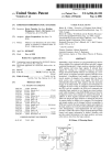
FIG. 5 is another vieW of the block diagram of FIG. 1,
shoWing a programmable logic device having an embedded
logic analyZer Within an electronic system.
FIG.6 is a block diagram of an embedded logic analyZer
circuit according to an embodiment of the present invention.
FIG. 7 is a block diagram of a typical computer system
suitable for implementing an embodiment of the present
invention.
output ?le Without the logic analyzer that represents the
engineer’s ?nal Working design. Thus, the logic analyZer
need not be part of the ?nal design and take up space on the
PLD.
The present invention is applicable to a Wide range of
hardWare devices, and especially to PLDs. A PLD in par
ticular may be implemented using a Wide variety of
technologies, including SRAM technology and EEPROM
technology. PLDs based upon SRAM technology are espe
10
cially advantageous in that they may have additional embed
ded memory that can be used by the embedded logic
analyZer to capture a large number of, and a greater depth of
In order to develop a design for programming an elec
tronic design such as a programmable logic device (PLD), a
signals. Furthermore, an embedded logic analyZer that is
designed and inserted automatically by an EDA tool means
that an engineer does not require an external logic analyZer
as a separate piece of equipment. Furthermore, the engineer
DETAILED DESCRIPTION OF THE
INVENTION
15
programmable logic development system is used. As used
herein, “electronic design” refers to circuit boards and
systems including multiple electronic devices and multi
may use the computer on Which he or she is creating a design
chip modules, as Well as integrated circuits. For
for the PLD to also control and con?gure the embedded
convenience, the folloWing discussion Will generally refer to
“integrated circuits”, or to “PLDs”, although the invention is
logic analyZer and to revieW its results.
In one embodiment of the present invention, a number of
pins on the PLD are dedicated interface pins for communi
cation With the user computer. Because these pins are
dedicated for the interface, and are knoWn ahead of time,
they may be routed to an easily accessible location or port
on a circuit board, such that a debugging interface cable may
be connected from the user computer to these pins extremely
not so limited.
Programmable Logic Development System
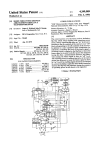
FIG. 1 is a block diagram of an embodiment of a
25
programmable logic development system 10 that includes a
computer netWork 12, a programming unit 14 and a pro
easily. This technique is especially advantageous Where pins
grammable logic device 16 that is to be programmed.
Computer netWork 12 includes any number of computers
or contacts of a particular integrated circuit in a package may
be dif?cult or nearly impossible to reach. Because the
connected in a netWork such as computer system A 18,
embedded logic analyZer of the present invention may be
system ?le server 23 all connected together through a
netWork connection 24. Computer netWork 12 is connected
via a cable 26 to programming unit 14, Which in turn is
connected via a programming cable 28 to the PLD 16.
computer system B 20, computer system C 22 and computer
con?gured to monitor any internal or external signals of the
PLD, all of these monitored signals are available for analysis
through these interface pins. In other Words, it is not
necessary to physically connect a probe to a particular
35
external pin of interest because any signal Within the PLD
can be monitored, stored Within the memory of the embed
netWork 12 need not be connected to programming unit 14
at all times, such as When a design is being developed, but
could be connected only When PLD 16 is to be programmed.
Programming unit 14 may be any suitable hardWare
ded logic analyZer and then later uploaded to the user
computer for analysis through these dedicated interface pins.
Additionally, an embedded logic analyZer can be used
With PLDs that are con?gured to near capacity. An engineer
can temporarily remove a portion of the design unrelated to
programming unit that accepts program instructions from
computer netWork 12 in order to program PLD 16. By Way
of example, programming unit 14 may include an add-on
the problem under analysis, embed a logic analyZer circuit,
and then debug the PLD. Once the PLD has been debugged,
the engineer may then remove the embedded logic analyZer
and reinsert that section of the design that he had temporarily
logic programmer card for a computer, and a master pro
gramming unit, such as are available from Altera Corpora
tion of San Jose, Calif. PLD 16 may be present in a system
or in a programming station. In operation, any number of
engineers use computer netWork 12 in order to develop
removed.
BRIEF DESCRIPTION OF THE DRAWINGS
programming instructions using an electronic-design auto
mation softWare tool. Once a design has been developed and
entered by the engineers, the design is compiled and veri?ed
before being doWnloaded to the programming unit. The
The invention, together With further advantages thereof,
may best be understood by reference to the folloWing
description taken in conjunction With the accompanying
draWings in Which:
FIG 1 is a block diagram of a programmable logic
development system according to one embodiment of the
present invention.
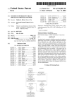
FIG. 2 is a ?oWchart of a design methodology used to
design a programmable logic device according to one
embodiment of the present invention.
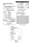
FIGS. 3A and 3B are a ?oWchart describing one technique
by Which signals are speci?ed for a logic analyZer to be
Alternatively, only one computer system could be directly
connected to programming unit 14. Furthermore, computer
55
programming unit 14 is then able to use the doWnloaded
design in order to program PLD 16.
For the purposes of debugging a PLD according to an
embodiment of the present invention, any of the computers
shoWn or others may be used to specify a logic analyZer
circuit and to compile such circuit along With a user’s
design. Furthermore, programming cable 28 may be used to
control the logic analyZer and to receive data from it, or a
separate debugging cable may be used to directly connect a
computer With device 16.
embedded Within a device so that the signals may be
captured and vieWed by a user.
Such a programmable logic development system is used
FIG. 4 is a ?oWchart describing a technique by Which a 65 to create an electronic design. Design entry and processing
occurs in the context of a “project”. A project includes a
logic analyZer may be compiled along With a user’s design
to embed the logic analyZer Within a hardWare device.
project ?le, design ?les, assignment ?les, and simulation
US 6,389,558 B1
7
8
?les, together With hierarchy information, system settings,
may need only add syntax de?ning a particular AND gate
and output ?les, Which includes programming ?les and
operation. Normal design, such as VHDL or other IEEE
report ?les. A project database may also exist, Which con
tains intermediate data structures and version information.
standard, requires large amounts of text to adequately set up
the design block.
A project contains one or more hierarchies of design
Those skilled in the art Will recogniZe that design ?le
entities and each design hierarchy tree has a root entity,
templates such as these can be used as starting points for the
design of the structural or functional entities needed by the
design. Thus, a design ?le template may serve as a reusable
Which is the topmost design entity in that hierarchy tree (the
top-level functional block). Other design entities in the
design hierarchy tree are called child entities. Also, a design
hierarchy may contain entities for Which there is no corre
object for different instances of a block in one or more
10
sponding design ?le, for example, in a top-doWn design
methodology. That part of a hierarchy Which contains such
not-yet-implemented entities is not compiled or simulated
until a design ?le is supplied for each entity. In this case,
template source ?les are automatically generated Which have
de?ned interfaces but empty bodies to assist in implement
ing these parts of a project. A user creates a design by
specifying and implementing functional blocks, as Will noW
be described in the context of an exemplary design meth
employed to reduce the amount of labor that the designer
must expend to generate the logic in the blocks. In one
embodiment, the generation of the design ?le templates is
done in such a Way that the templates can be updated later
15
Next, in step 58, each of the blocks of the top-level block
diagrams (i.e., blocks Within blocks). If changes are required
at the top-level then the top-level block diagram is updated
and the sub-designs are preferably automatically updated as
Design Methodology
to program a PLD. It should be appreciated that the present
invention may be practiced in the context of a Wide variety
Well.
Furthermore, a block may be compiled through to a ?tting
25
This sequence illustrates a style of design in Which an
engineer ?rst designs, then compiles and simulates, and then
returns to design again if the simulation results are not
satisfactory. In another style, an engineer may iterate
through a number of design folloWed by simulation loops
before ?nally compiling the complete design.
35
like. The multiple engineers Within a Work group Will use
this system speci?cation in order to create a design With the
EDA tool that Will then be used to program a PLD.
Concerning block implementation order, one or more of
the folloWing factors can be used to determine implemen
tation order: (1) the complexity of a block; (2) the uncer
tainty or risk associated With a block; and/or (3) hoW far
upstream and/or doWnstream in a given data-path the block
resides. Each of steps 60, 62, 64, 68 and 70 may also lead
back to this block implementation step for additional imple
mentation necessitated by later changes in the design.
Once the system speci?cation is obtained, creation of a
design using functional block diagrams is begun. In step 54
In step 60 a block is simulated functionally at the source
a top-level block diagram is created in Which connections
betWeen loWer-level designs blocks are speci?ed. In this
block, the target device, speed grade, and key timing
stage for a particular integrated circuit die to provide infor
mation about resource utiliZation, timing performance, etc.,
as required for a given design. As such, it is envisioned that
some timing optimiZation may be performed during step 58.
of design methodologies. By Way of example, the Work
group computing techniques and system of the present
invention Work Well With an electronic design automation
(EDA) softWare tool Within the frameWork of the method
ology of FIG. 2.
In step 52 a system speci?cation for the PLD to be
programmed is obtained. This speci?cation is an external
document or ?le that describes, for example, the device pin
names, the functionality of each of the pins, the desired
system functionality, timing and resource budgets, and the
if the top-level block diagram changes.
is implemented using the EDA tool. It is noted that for more
complicated designs, there may be additional levels of block
odology.
FIG. 2 shoWs a design methodology 50 for using a system
design speci?cation in order to develop a design With Which
designs. More importantly, design ?le templates Will be
45
level using a behavioral simulator and vectors generated by
using a VHDL or Verilog test bench, for example. The
requirements may be speci?ed. Those skilled in the art Will
recogniZe that this top-level block may also include blocks
that have already been developed or implemented or that
have been obtained from a third party provider. This top
simulation results can then be displayed or otherWise
presented/recorded as Waveforms, text or annotated onto the
source ?les. The designer may also return to step 58 to
level block may also be converted into an HDL ?le, or the
like, for use in other related design tools, such as an external
simulator.
compiled or a timing analysis performed.
Once the designer is satis?ed With the simulation results,
implement a block again. Also, at this point a block may be
Step 56 includes generating design ?le templates With the
EDA tool for all blocks present in the top-level block
diagram of step 54. After the designer has created a block
Which has not yet been implemented, the system may
55
generate a design ?le template. Such templates may display
a block in a WindoW format including, for example, a title,
a date, etc. around the boundaries. It may also include some
in step 62 the block is combined With other blocks and the
resulting group is simulated together. In some cases, it may
be useful to complete a full compilation to provide critical
resource and timing information. Also, output simulation
vectors from one block may-become the input simulation
vectors to the next block. The designer may also return to
step 54 to modify the top-level block or to step 58 to
implement a block again.
Next, in step 64, the entire design is simulated function
details of the functional content depicted Within the WindoW.
The design ?le templates may be in any speci?ed design
ally at the source level using a behavioral simulator.
format including VHDL, AHDL, Verilog, block diagram,
Preferably, the top-level block diagram is fully speci?ed
schematic, or other like format. In the case of a VHDL block
before simulation and shoWs complete design connectivity.
the template may also include much of the formatting and
necessary syntax for any VHDL block. The user need only
take the template and add the small portion of VHDL syntax
required to implement his function. For example, the user
Vectors can be generated using a VHDL or Verilog test
65
bench. Again, the simulation results can be displayed either
as Waveforms or annotated onto the source ?les. The
designer may also return to step 54 to modify the top-level
US 6,389,558 B1
10
block or to step 58 to implement a block again. In step 66
design ?les Will be augmented With a logic analyZer accord
the entire design is compiled through to a ?le containing the
ing to one embodiment of the present invention and is
described in greater detail in FIG. 4. This debugging feature
also alloWs the combined netlist to be processed and pro
grammed onto the device.
Next, the user is able to program the logic analyZer in
order to debug the device in any Way that the engineer
information needed to program a PLD to implement the
user’s design, such as to a “programming output ?le”.
A Wide variety of compile techniques may be used
depending upon the type of design being created. By Way of
example, a feW examples of compilation are presented
beloW. For a PLD, compilation includes the steps of
chooses. One such logic analyZer circuit is shoWn in FIG. 6;
synthesis, place and route, generation of programming ?les
the design for the logic analyZer may already be present
and simulation. For a traditional integrated circuit design
With a custom layout, compilation includes a layout version
schematic, a design rule checker and simulations. For inte
Within the EDA tool, or may be generated at any time. In step
108, the signals of interest of the device to be monitored are
grated circuit design using a high level design tool, compi
lation includes synthesis from a language such as VHDL or
Verilog, automatic place and route and simulations. For
15
speci?ed. These are the signals that a user Wishes to vieW in
order to track doWn the cause of the malfunction. The signals
may be those present on pins of the device, or any internal
signals or points Within the device. Often the nature of the
printed circuit boards, compilation includes automatic
routing, design rule checking, lumped parameter extraction
malfunction observed in step 104 Will provide a clue,
and simulation. Of course, other types of compilation and
mation about the problem. For example, if the malfunction
is associated With data output at a particular pin, the signals
to be monitored may be provided by logic upstream from the
suggesting signals that Would likely provide further infor
variations on the above are possible.
Within the context of the present invention, any of the
above compile techniques may be modi?ed in order to
produce an embedded logic analyZer. As Will be discussed in
greater detail beloW With reference to FIG. 4, the compila
tion of a PLD is modi?ed in order to insert a logic analyZer
into a user’s design.
pm.
These signals to be monitored may be speci?ed in a Wide
variety of Ways. By Way of example, a hierarchical path
FolloWing compilation in step 66, in step 68 the timing
name for each signal may be speci?ed, or a graphical user
interface may be used to vieW a particular design ?le and to
select a signal or point from Within that ?le to be monitored.
checker inside the compiler is used to determine if the
At this time, the user may also specify Which pins of the
performance goals for the design have been met. Also,
device Will be used as an interface to the user computer, i.e.,
timing simulations are used to check performance details. In
addition, other analysis tools such as a design pro?ler and/or
layout editor can be used to further optimiZe the perfor
mance of the design. Preferably, optimiZation is not per
embedded logic analyZer Within the PLD and to upload
captured information from the logic analyZer to the user
formed prior to step 68 because full compilation is usually
In step 110, the number of samples to be captured are
25
those pins to be used to send control information to the
computer.
required to establish the location of one or more critical 35 speci?ed. In other Words, the depth of the capture buffer is
paths Within the design. The designer may also return to step
54 to modify the top-level block or to step 58 to implement
speci?ed and this, in turn, indicates hoW many clock pulses
of data Will be acquired by the logic analyZer. In one
a block again.
embodiment of the invention, a PLD that includes embedded
memory blocks (such as any of the FLEX 10K family of
devices available from Altera Corporation) Works Well for
implementing the present invention. The embedded memory
Next, in step 70 the device is programmed/con?gured
using programming unit 14 and tested in the system. Again,
the designer may also return to step 54 to modify the
top-level block or to step 58 to implement a block again.
blocks are easily programmed to provide relatively large
buffers (as part of the logic analyZer circuit) for the storage
While methodology 50 presents a top-doWn design process,
it may also be used to support a bottom-up type methodol
ogy. NoW that a general design methodology has been
described by Which an engineer may develop a design for a
PLD, a technique for embedding a logic analyZer Within a
of captured information. Embedded memory devices are not,
45
PLD Will noW be discussed.
Embedded Logic AnalyZer
hoWever, necessary for the buffering of information cap
tured. Although devices Without embedded memory may be
used With the present invention, they just do not lend
themselves as easily to creation of relatively large buffers. In
devices Without embedded memory, buffers may be imple
mented over multiple cells, using available memory from
each cell.
The ?oWchart of FIGS. 3A and 3B describe one possible
technique by Which a user may utiliZe the present invention
in order to embed a logic analyZer Within a PLD to capture
desired signals and to vieW the results on a computer. In step
In step 112, a system clock signal is speci?ed for use by
the logic analyZer. Any of a variety of signals available
Within the device may be speci?ed as a system clock signal.
102 a user generates a design for a device and compiles the 55 A device clock signal that is relevant to the signals being
design into an output ?le. AWide variety of EDA tools may
be used to generate and compile a design for a PLD. By Way
monitored Will typically be chosen as a system clock signal.
of example, the technique disclosed in US. patent Applica
condition may include any number of trigger signals to
monitor and the logic levels that those trigger signals must
In step 114, the trigger condition is speci?ed. A trigger
tion Serial No. 60/029,277 may be used.
In step 104, the compiled output ?le is used to program
have in order for the logic analyZer to trigger. I.e., the trigger
the device and the device is placed under operating
condition describes a particular state of the device. When the
conditions, such as on a printed circuit board or Within a
logic analyZer is triggered, it begins acquisition of data for
the signals being monitored. Any number of trigger signals
suitable electronic system. At this step, an engineer may
observe malfunctions With the device. If so, then in step 106
a hardWare debugging feature of the EDA tool is enabled.
This enablement Will alloW the EDA tool to perform netlist
augmentation. That is, the engineer’s design in various
65
or trigger states may be speci?ed to de?ne the trigger
condition. Atrigger may be as simple as one signal changing
state, or may be a complex pattern of signals or a sequence
of patterns that must occur before the logic analyZer is
US 6,389,558 B1
11
12
triggered. Also, a trigger condition need not be speci?ed in
all cases; if not, the logic analyzer triggers immediately upon
being armed. Advantageously, the trigger condition can be
as if an external logic analyZer had been able to be connected
to these signals.
FIG. 4 is a ?oWchart 200 that describes a technique by
changed at any time by the user through the use of the EDA
tool, and a neW trigger condition can be doWnloaded to the
embedded logic analyZer in the device Without having to
recompile all of the device design ?les. By alloWing trigger
conditions to be changed rapidly for a device Within a
system, debugging is much more ef?cient.
Once the user has speci?ed hoW he Wishes the embedded
logic analyZer to function, the complete design is compiled.
10
circuits. The embodiment of FIG. 4 illustrates hoW the
present invention may be used With one such compilation
In step 116, the user issues a compile command in order to
compile the user’s device design along With the logic
analyZer design that has been speci?ed. In a preferred
embodiment of the invention, the user’s design ?les are not
modi?ed during this process. The logic analyZer design is
incorporated into the output ?les produced. In one speci?c
technique, although it is contemplated that the present
invention is applicable to any of a Wide variety of compi
15
as a PLD. These design ?les may often specify the design
implement step 116.
elements for the design. In many design environments, the
design elements are arranged in a hierarchy, from root entity
The result of this step is a neW output ?le that includes the
user design With an embedded logic analyZer. Atechnique by
to leaf entities. In such cases, if the design uses a particular
Which an EDA tool may insert a custom logic analyZer in a
25
reprogrammed using the neW output ?le.
register in numerous locations throughout the design, there
may be only one ?le containing the implementation of this
design, yet the complete design may reference that one ?le
in numerous locations. Examples of such electronic design
?les are discussed above With reference to FIGS. 1 and 2.
In step 120, the user connects a debugging interface cable
from the device to the user computer. The interface cable
may be the same cable used to program the device or it may
be a dedicated cable for debugging. In one embodiment of
Step 204 takes these user design ?les and generates a
?attened netlist representation of the user design. In other
Words, should the design ?les include a hierarchy, this
hierarchy is “?attened out” so that each entity referenced in
the design is duplicated as many times as it is used. Using
the above example, if a particular register is used tWice in the
design hierarchy, yet only one ?le exists to describe this
the invention, the debugging cable connects to pins that have
been speci?ed by the user in step 108 as being dedicated to
the logic analyZer circuit. In other Words, if the user has
speci?ed the pins to Which the debugging cable Will be
connected, the cable should be connected to those pins. In an
alternative embodiment, the user does not have the option to
lation techniques.
In step 202 an EDA tool accepts the user design ?les
necessary to describe an electronic design for a device such
embodiment, the process shoWn in FIG. 4 may be used to
user design Will be discussed in greater detail beloW With
reference to FIG. 4. Once the neW output ?le has been
generated, then in step 118 the device Within its system is
Which a logic analyZer circuit may be automatically inserted
into, and automatically compiled along With, a user design.
The technique of FIG. 4 is a suitable technique by Which step
116 of FIG. 3B may be implemented (in the context of PLD
compilation). It should be appreciated that a variety of
compilation techniques may be used With the various EDA
tools, for PLD design as Well for other types of integrated
35
register, this step ?attens out the design by producing tWo
such ?les for the register. The representation of the user
design in this step is preferably a synthesiZed technology
mapped database that Will be appreciated by those of skill in
specify the “debugging pins,” rather the system speci?es
them automatically. The signals from these pins may be
routed to an easily accessible location or port on the board
the art. At this point in the compile process, a synthesiZed
to Which the debugging cable may easily attach. The cable
netlist of the user design has been created in a ?attened state.
Typically, generation of such a netlist is referred to as a
Will be used to transmit instructions from the computer to the
“synthesis” step in the compilation process, after elaboration
embedded logic analyZer, and also to upload captured infor
has occurred.
mation from the logic analyZer to the computer. In a pre
ferred embodiment of the invention, the cable is a serial
In step 206, a gate level representation of the logic
interface and uses as feW as four pins on the device. As 45 analyZer circuit is produced. The logic analyZer circuit may
take a Wide variety of forms. By Way of example, logic
discussed beloW, FIG. 5 shoWs a PLD containing both a user
analyZer circuit 260 of FIG. 6 may be used, although it
should be appreciated that a logic analyZer circuit may be
implemented in many Ways While still performing the func
tionality of the circuit shoWn in FIG. 6. In a preferred
embodiment of the invention, a logic analyZer circuit is
design and an embedded logic analyZer Within an electronic
system. A cable is shoWn connecting the electronic system
to an external computer.
In step 122 the user through the EDA tool arms the
embedded logic analyZer With an appropriate command.
included in the EDA tool so that a gate level representation
may be produced automatically. Alternatively, a user could
be alloWed to specify a custom circuit. This gate level
This may be at the time When the user begins execution of
the system in Which the device is operating, although arming
need not occur contemporaneously With system operation.
Preferably, the user manipulates the system to duplicate
previous malfunctions that the user Wishes to analyZe. In
step 124, once the trigger condition is satis?ed, the embed
ded logic analyZer Will capture the signals speci?ed up to a
speci?ed depth and store them in a memory of the logic
55
samples to be captured speci?ed in step 110, and the trigger
signals and a trigger condition as speci?ed in step 114. Those
of skill in the art Will appreciate the process by Which a gate
level representation of a particular circuit is produced.
The actual gate level representation of a particular logic
analyZer. The logic analyZer is then able to upload this stored
information over the serial interface cable to the user’s
computer. In step 126 the user is able to graphically vieW
these signals received from the logic analyZer. In one
embodiment, the signals are presented in a Waveform vieW
annotated With the names of the signals. Thus, by vieWing
representation takes into account each logic element of the
circuit, along With the number and names of the signals to
monitor speci?ed by the user in step 108, the number of
65
analyZer circuit Will depend upon the particular device in
Which the logic analyZer Will be embedded. By Way of
example, the hardWare device in Which to embed the logic
these signals of interest on a computer, a user is able to
analyZer may include any of the PLD devices available from
ef?ciently debug a hardWare device in much the same Way
Altera Corporation. In particular, any of the FLEX 10K,
US 6,389,558 B1
13
14
FLEX 8000, MAX 9000, or MAX 7000 devices Work Well.
Each of these particular devices may have different features
that Would affect hoW a gate level representation for a logic
system. PLD 16 has been con?gured With a user logic design
256 and an embedded logic analyZer 260. User logic 256 is
con?gured With a design according to the methodology
analyZer is produced. For example, for a FLEX 10K device
described in FIG. 2, or any other suitable design method
With relatively large embedded memory sections, this
embedded memory is particularly Well suited for implement
ing a large FIFO (?rst in ?rst out) memory for the logic
ology. Embedded logic analyZer 260 has been incorporated
into PLD 16 according to one embodiment of the invention
described in FIGS. 3A and 3B.
analyZer. For a device such as the FLEX 8000 Without
embedded memory, the memory elements (such as SRAM
?ip-?ops) of logic cells may be used for the memory of the
logic analyZer but the FIFO buffer may have to be divided
10
Logical connections 262 alloWs signals from user logic
256 to be transmitted to logic analyZer 260. These signals
may include a system clock, trigger signals, signals to
monitor, etc. Pins of PLD 16 are used to connect debug
over multiple cells if the memory in a single cell is not
interface signals 264 from the logic analyZer to correspond
sufficiently large to accommodate the buffer. Similarly, a
ing connections 266 in electronic system 252. Cable 28 is
used to connect these debug interface signals to computer
18. Alternatively, computer 18 may be directly connected to
PLD 16 to transmit debug interface signals 264 to the PLD.
In this manner, computer 18 transmits commands and other
information to embedded logic analyZer 260, and receives
device based upon EEPROM technology may also use one
or more of its logic cells for the logic analyZer’s buffer. A
device having large embedded memory Works particularly
15
Well With the present invention because of the larger capac
ity for signal storage. Thus, step 206 produces a represen
tation for a logic analyZer circuit that is to be connected to
the user’s design.
In step 208 the gate level representation of the logic
20
analyZer circuit from step 206 is connected to the ?attened
representation of the user design of step 204. This step
makes the logic connections from the inputs of the logic
analyZer (trigger signals, system clock, signals to monitor)
to lines providing the actual signals speci?ed in the user’s
25
design. As those signals have previously been speci?ed in
steps 108 through 114, the EDA tool is able to ?nd the
particular signal lines Within its database representation of
the electronic design and to make the appropriate connection
to an input of the logic analyZer.
In addition, this step makes appropriate connections from
the logic analyZer to an interface to the user’s computer. In
the embodiment of FIG. 6, discussed beloW, this interface
30
information from the logic analyZer Without directly inter
rupting or affecting the functional operation of electronic
system 252. PLD 16 is thus con?gured to perform both the
functions of user logic 256 and embedded logic analyZer
260.
FIG. 6 is a block diagram of embedded logic analyZer 260
according to one embodiment of the present invention. A
logic analyZer to be embedded Within a PLD may be
implemented in a Wide variety of manners depending upon
the type of PLD, signal type and number to be monitored,
depth of data desired, memory available, control signals
from the user’s computer and preferences of the designing
engineer, etc. By Way of example, logic analyZer 260 is one
particular example of hoW such a logic analyZer may be
implemented. The embedded logic analyZer is controlled by
the user from a computer external to the PLD and operates
includes four signals available at the logic analyZer, namely: 35 to capture any of a variety of internal signals that the user
serial data in, mode select, debug clock, and serial data out.
Wishes.
Of course, another embodiment of a logic analyZer circuit
Once logic analyZer 260 has been programmed into a
PLD, it receives a variety of inputs from signals Within the
PLD. Collectively, these signals are called logic
connections, or system interface signals 262. Signals to
may use different signals and/or a greater or feWer number
of interface signals. In a preferred embodiment of the
invention, these interface signals to and from the logic
40
monitor 302 are those signals internal to the PLD that the
analyZer are connected to four dedicated pins on the PLD
reserved for this purpose. Thus, a user Will knoW to Which
four pins the debugging cable should be attached. As noted,
these pins not only control the embedded logic analyZer, but
also receive data from it. In other embodiments, the four pins
may be routed to another part of the circuit board for easy
attachment of a cable. In this fashion, the logic for the logic
analyZer circuit created in step 206 is connected to the user
design and to interface pins of the PLD for communication
With the user computer.
user had speci?ed in step 108 to be monitored by the logic
analyZer. System clock 304 is the system clock speci?ed in
step 112 that the user Wishes to clock input to the logic
45
analyZer. Trigger signals 306 are those signals speci?ed in
step 114 that the user Wishes to compare to a trigger
In step 210 the complete design created in step 208 is
placed and routed in a fashion that Will be appreciated by
condition 308 that Was also speci?ed in step 114.
Logic analyZer 260 also communicates With an external
computer from Which it receives commands and other
information, and to Which it transfers information including
the current status of logic analyZer 260 and data captured
from the PLD. Such communication may take place in a
those of skill in the art. The output of the place and route step
is then input to step 212 in Which the output ?le is
Wide variety of forms. By Way of example, in the embodi
ments shoWn, communication takes place over four pins of
50
assembled. This output ?le may then be doWnloaded to a 55 the PLD using a serial interface constituting a debug inter
PLD in order to program it. Once a PLD has been pro
face 264. Of course, any number of pins may be used to
perform a similar function.
grammed With this ?le, a user may begin use of the embed
ded logic analyZer in order to debug the device.
FIG. 5 is another vieW of programmable logic develop
ment system 10 of FIG. 1, shoWing a programmable logic
Pins 320 and 322 transmit signals “serial data in” and
“mode select” from the computer to the logic analyZer.
60
“Serial data out” pin 326 transmits data or status information
tially shares one or more electronic connections 254 With the
from logic analyZer 260 to the external computer. The
“debug clock” pin 324 is connected to a debug clock signal
provided by the external computer, Which is used to syn
chroniZe the serial transmission of commands, data and
other information from the external computer to the logic
analyZer, and from the logic analyZer to the external com
other components and elements that make up the electronic
puter.
device having an embedded logic analyZer Within an elec
tronic system. System 10 shoWs an electronic system 252
connected to computer system A 18 via cable 28 or other
connective appliance. Electronic system 252 includes PLD
16, a component of the electronic system. PLD 16 poten
65
US 6,389,558 B1
15
16
Furthermore, a variety of commands may be issued by the
computer to the logic analyzer. In one speci?c embodiment,
counter 338 to step through addresses in memory 342. This
signal 352 is also sent to shift register 344 to enable it to
the logic analyzer recognizes four commands from the
convert the data Words from memory 342 into a serial
external computer. The computer may issue an “arm” com
mand to arm the logic analyzer, a “set trigger” command to
format. Signal 352 is also sent to serial data multiplexer 384
to alloW the serial data output signal 398 from shift register
344 to drive the serial data out pin 326. Upon receipt of a
“read status” command, debug mode state machine 330
set the value of trigger condition 308, an “unload data”
command to direct the logic analyzer to upload its data, or
sends a read status signal 392 to status register 382. When
a “read status” command in order to determine the current
status of the logic analyzer. Also, other information may be
transmitted from the external computer to the logic analyzer,
including information to prepare or con?gure the logic
analyzer. In this embodiment, the external computer can
transmit data to trigger register 380 in order to set the value
of trigger condition 308.
The logic analyzer may also transmit information to the
computer using these interface pins. For example, in this
10
15
embodiment, the current state of trigger state machine 332
may be “armed”, “running”, or “full”. A data value repre
senting the current state of trigger state machine 332 may be
transmitted to the computer using these pins.
It should be understood that in preferred embodiments,
the computer to Which pins 320, 322, 324 and 326 (or any
other pins in alternative embodiments) are connected per
forms the analysis function of the logic analyzer. The
circuitry provided on the PLD interior merely provides the
data acquisition component of the logic analyzer. Of course,
the logic necessary for data analysis could be provided on
trigger register 380. Trigger register 380 may be imple
mented as a shift register Which converts serial data from the
25
the PLD, and the serial data loaded into the trigger register
is used to modify the individual signals of trigger condition
308. This method is advantageous because it permits the
default trigger condition to be active Without loading the
trigger register at all.
merely to (a) control the state of the logic analyzer and (b)
vieW information output by the logic analyzer.
NoW that the inputs and outputs to the logic analyzer have
been described, its functionality Will noW be explained. In
Trigger state machine 332 may be implemented in a Wide
variety of Ways; in a preferred embodiment, state machine
this embodiment of the invention, logic analyzer 260
35
plexer 340, a memory 342, a shift register 344, a trigger
register 380, a status register 382 and a serial data multi
plexer 384. Of course, variations on the design of the logic
analyzer may be present depending upon a variety of factors
mentioned above.
In operation, debug mode state machine 330 receives
“complete, memory full”. The “never armed” state occurs
When the logic analyzer is ?rst embedded in a device and the
user has not yet armed it. The “armed and Waiting for
trigger” state occurs once the user delivers an “arm”
45
analyzer is full (depending upon the number of samples that
Trigger comparator 334 compares trigger signals 306 and
55
machine 332. Thus, based upon its various inputs, state
machine 332 is maintained in one of the four states and also
data into a trigger condition 308 Which is then sent to trigger
machine 330 sends a signal 352 to enable read address
their associated logic state to trigger condition 308. When
the tWo match, a trigger has occurred and logic 334 issues
“start” signal 356 to state machine 332. If trigger state
machine 332 is armed then upon receipt of “start” signal
356, state machine 332 issues a “running” signal 360 to
enable counter 336 to step through addresses in memory
342. The “running” signal 360 is also sent to memory 342,
enabling memory 342 to capture and store the signals to
monitor 302. Once counter 336 has reached the last address
in memory 342, it issues “last address” signal 358 to state
signal 390 to trigger register 380, enabling it to receive data
from serial data in pin 320. Trigger register 380 converts this
comparator 334.
Upon receipt of an “unload data” command, state
command, and the “triggered and running” state occurs once
a trigger condition is met. When the memory of the logic
the user Wishes to capture), then the trigger state machine
enters the “complete, memory full” state.
operation occurs noW folloWs.
Auser is able to issue the commands “arm”, “set trigger”,
“unload data”, and “read status” from a computer via signals
present on debug interface 264. Debug mode state machine
330 receives and processes these commands and may be
implemented in any suitable fashion. Upon receipt of an
“arm” command, state machine 330 sends an “arm” signal
350 to trigger state machine 332. Upon receipt of a “set
trigger” command, state machine 330 sends a set trigger
332 is a synchronous state machine. The inputs to state
machine 332 are system clock 304, “arm” signal 350, a
“start” signal 356 and a “last address” signal 358. State
machine 332 has four states: “never armed”; “armed and
Waiting for trigger”; “triggered and running”; and
commands from the user computer and processes them.
When the logic analyzer is armed and a trigger occurs,
trigger state machine 332 alloWs Write address counter 336
to step through memory addresses in memory 342 thus
storing signals 302. When the user Wishes to upload data
from the logic analyzer, state machine 330 directs read
address counter 338 to step through addresses in memory
342 and thus outputs data serially to the user computer via
shift register 344. A more detailed explanation of hoW
serial data in signal 320 into a parallel format, Which is
stored as trigger condition 308. Alternatively, serial data
from serial data in signal 320 could be used to select the
value of trigger condition 308 using any suitable method.
For example, in one speci?c embodiment, a particular value
of trigger condition 308 is established as the default value
before the logic analyzer is compiled and programmed into
the PLD, in Which case the external computer Would be used
includes a debug mode state machine 330, a trigger state
machine 332, a trigger comparator 334, a Write address
counter 336, a read address counter 338, an address multi
this signal is present, status register 382 shifts the values of
status bits out on output signal 396, through serial data
multiplexer 384 to serial data out pin 326. In this fashion, the
external computer may issue commands to the logic
analyzer, transmit data to the logic analyzer, and receive data
from the logic analyzer via debug interface 264. In
particular, the external computer may determine the status of
the logic analyzer at any time via debug interface 264.
When the user has issued a “set trigger” command, debug
mode state machine 330 sends “set trigger” signal 390 to
65
indicates this state via state signals 360, 386 and 388 to
status register 382.
Write address counter 336 passes its address through
address multiplexer 340 before being delivered as address
368 to memory 342. Address multiplexer 340 may be any
suitable type of multiplexer. The “running” signal 360 from
US 6,389,558 B1
17
18
state machine 332 also serves as a select signal to address
provides additional data storage capacity and may also
include any of the computer-readable media described
multiplexer 340 to control Whether Write addresses or read
addresses are passed through to memory 342. When trigger
state machine 332 is in the “running” state it sends the
“running” signal 360 to address multiplexer 340, causing it
beloW. Mass storage device 908 may be used to store
programs, data and the like and is typically a secondary
storage medium (such as a hard disk) that is sloWer than
to connect the Write address 366 to the address 368 of
memory 342. OtherWise the read address 394 is connected
to address 368 of memory 342.
primary storage. It Will be appreciated that the information
retained Within mass storage device 908, may, in appropriate
cases, be incorporated in standard fashion as part of primary
In this example, memory 342 has a Width representing
symbolically the depth, or number of samples to store in
memory, While the height of memory 342 represents sym
bolically the siZe of a Word stored. The number of samples
stored in memory 342 also indicates the siZes of counters
336 and 338. Memory 342 may be implemented in a Wide
variety of Ways. By Way of example, in one embodiment of
the invention, logic analyZer 260 is embedded in a FLEX
10K PLD available from Altera Corporation. This particular
PLD contains embedded SRAM memory in Which it is
useful to implement memory 342. Of course, memory 342
may be implemented in many other types of PLDs that do
not contain extra embedded memory. In this example,
memory 342 is implemented as a ?rst-in ?rst-out (FIFO)
10
one or more input/output devices such as such as video
monitors, track balls, mice, keyboards, microphones, touch
15
telecommunications netWork using a netWork connection as
is contemplated that the CPU might receive information
from the netWork, or might output information to the net
Work in the course of performing the above-described
When the user has issued an “unload data” command, 25
debug mode state machine 330 sends “unload data” signal
352 to enable read address counter 338 to begin counting.
Address 394 passes through address multiplexer 340 to
select successive Words in memory 342. A Word at a time
Shift register 344 (also called a parallel-to-serial converter)
may be of any siZe and implemented in any fashion. Words
of any siZe may also be stored in memory 342 and trans
mitted to an external computer either via serial or a parallel
35
372 and shifts out a bit at a time using debug clock 324
functioning as a bit clock. Load enable signal 372 is sent by
read address counter 338 to shift register 344 each time the
value of address 394 is changed, to cause shift register 344
to load the corresponding data Word 370 from memory 342.
Read address counter 338 increments address 394 every N
media such as ?optical disks; and hardWare devices that are
such as ROM and RAM devices. Examples of program code
include both machine code, such as produced by a compiler,
and ?les containing higher level code that may be executed
by the computer using an interpreter.
Although the foregoing invention has been described in
in data Word 370. Successive Words from memory 342 are
shifted serially out via serial data signal 398, through serial
45
“unload data” signal 352 is active, serial data multiplexer
384 connects shift register output signal 398 to serial data
out pin 326. OtherWise it connects status register output
signal 396 to serial data out pin 326. In this manner, signals
some detail for purposes of clarity of understanding, it Will
be apparent that certain changes and modi?cations may be
practiced Within the scope of the appended claims. For
instance, a logic analyZer may be embedded in any suitable
device or circuit board that lends itself to being pro
grammed. Also, the present invention is applicable to any
type of EDA tool that is able to compile a user design.
stored in memory 342 after a trigger condition may even
tually be transferred to an external computer.
Although only one example of compilation of a logic
analyZer is presented, variations on this compile technique
Computer System Embodiment
may occur depending upon the device for Which the design
55
system 900 includes any number of processors 902 (also
referred to as central processing units, or CPUs) that are
coupled to storage devices including primary storage 906
(such as random access memory, or RAM) and primary
storage 904 (such as a read only memory, or ROM). As is
Well knoWn in the art, primary storage 904 acts to transfer
data and instructions uni-directionally to the CPU and
primary storage 906 is used typically to transfer data and
instructions in a bi-directional manner. Both of these pri
mary storage devices may include any suitable of the 65
computer-readable media described beloW. A mass storage
device 908 is also coupled bi-directionally to CPU 902 and
media such as hard disks, ?oppy disks, and magnetic tape;
optical media such as CD-ROM disks; magneto-optical
specially con?gured to store and execute program code,
cycles of debug clock 324 Where N is the number of signals
FIG. 7 illustrates a computer system 900 in accordance
With an embodiment of the present invention. Computer
method steps.
In addition, embodiments of the present invention further
relate to computer storage products With a computer read
able medium that have program code thereon for performing
various computer-implemented operations. The media and
program code may be those specially designed and con
structed for the purposes of the present invention, or they
may be of the kind Well knoWn and available to those having
skill in the computer softWare arts. Examples of computer
readable media include, but are not limited to: magnetic
370 is transferred from memory 342 into shift register 344.
data multiplexer 384 to serial data out pin 326. When
sensitive displays, transducer card readers, magnetic or
paper tape readers, tablets, styluses, voice or handWriting
recogniZers, biometrics readers, or other computers. CPU
902 optionally may be coupled to another computer or
shoWn generally at 912. With such a netWork connection, it
memory. Memory 342 stores signals 302 When “running”
signal 360 enables the memory for Writing.
interface. Shift register 344 is loaded via load enable signal
storage 906 as virtual memory. A speci?c mass storage
device such as a CD-ROM 914 passes data uni-directionally
to the CPU.
CPU 902 is also coupled to an interface 910 that includes
is being compiled and still take advantage of the present
invention. Furthermore, the speci?c logic analyZer circuit
shoWn is exemplary; other circuits may also be used to
implement a logic analyZer. An interface to the logic ana
lyZer from a computer may use any number of pins and any
type of protocol such as serial, parallel, etc. Therefore, the
described embodiments should be taken as illustrative and
not restrictive, and the invention should not be limited to the
details given herein but should be de?ned by the folloWing
claims and their full scope of equivalents.
We claim:
1. Aprogrammable logic development system arranged to
debug a programmable logic device (PLD), said system
comprising:
US 6,389,558 B1
19
20
11. A method as recited in claim 10 Wherein said PLD is
a PLD including
a logic analyzer integrated With user logic, and
a ?eld programmable gate array (FPGA).
interface pins;
12. A method as recited in claim 10 Wherein said logic
analyZer includes a trigger register for storing a trigger
condition, and Wherein said trigger condition may be modi
a computer having software arranged to deliver control
signals to said integrated logic analyZer via said inter
face pins; and
?ed by a user Without recompiling said modi?ed electronic
design.
a communication medium in electrical communication
13. A method as recited in claim 10 Wherein said modi?ed
betWeen said computer and said interface pins of said
PLD, said communication medium being arranged to
deliver said control signals to said PLD.
electronic design includes
control logic arranged to communicate betWeen said logic
analyZer and interface pins of said PLD.
2. A system as recited in claim 1 Wherein said PLD is a
14. A method as recited in claim 10 Wherein said elec
?eld programmable gate array (FPGA).
tronic design and said logic analyZer are represented using
a hardWare description language (HDL).
3. A system as recited in claim 1 Wherein said integrated
logic analyZer includes a trigger register for storing a trigger
condition, and Wherein said control signals include signals
arranged to modify said trigger condition, Whereby said
15. A method as recited in claim 10 Wherein said step of
compiling includes the sub-steps of:
synthesiZing said modi?ed electronic design; and
placing and routing said modi?ed electronic design.
trigger condition may be modi?ed by said user Without
recompiling said user logic.
4. A system as recited in claim 1 further comprising:
a circuit board on Which is mounted said PLD.
20
5. Asystem as recited in claim 1 Wherein said PLD further
includes
control logic arranged to communicate betWeen said
integrated logic analyZer and said interface pins of said
PLD, Wherein said control signals are delivered to said
25
integrated logic analyZer via said control logic as Well
16. A method as recited in claim 10 further comprising:
receiving a name of a trigger signal, said trigger signal
corresponding to one of said internal signals;
connecting said trigger signal to a trigger input of said
logic analyZer, such that When said compiled design is
doWnloaded to said PLD and said trigger signal
matches a trigger condition said logic analyZer is
arranged to begin storing data from said selected inter
nal signals.
as said interface pins.
6. A system as recited in claim 1 Wherein said commu
nication medium is a cable.
17. A method as recited in claim 10, Wherein said logic
analyZer includes a ?rst trigger condition, said method
7. Asystem as recited in claim 6 Whereby internal signals
of said user logic are captured by said integrated logic
analyZer and transmitted to said computer via said cable for
further comprising:
programming said PLD With said compiled design; and
sending a second trigger condition to said logic analyzer
vieWing by a user.
8. A method of compiling a logic analyZer along With an
electronic design for a programmable logic device (PLD),
said method comprising:
receiving an electronic design for a programmable logic
device (PLD), said electronic design including a plu
35
design, Whereby said logic analyZer is arranged to
begin monitoring said selected internal signals upon
occurrence of said second trigger condition.
18. Amethod as recited in claim 10, Wherein said selected
rality of internal signal lines;
internal signals include original signals, said method further
comprising:
receiving a representation of a logic analyZer to be
integrated With said electronic design;
connecting selected internal signal lines of said electronic
design to inputs of said logic analyZer; and
a step of performing the function of compiling said
programming said PLD With said compiled design such
that said logic analyZer is integrated Within said PLD;
receiving names of neW internal signals, said neW internal
45
electronic design along With said logic analyZer to
produce a compiled design suitable for programming
nals;
said PLD.
neW internal signals are connected to said inputs of said
logic analyZer; and
reprogramming said PLD With said recompiled modi?ed
electronic design, Whereby said logic analyZer is
said PLD.
arranged to monitor said neW internal signals.
19. A method as recited in claim 10, Whereby said logic
analyZer is arranged to store data from said selected internal
signal lines When said compiled design is doWnloaded to
10. A method of compiling a logic analyZer along With an
electronic design for a programmable logic device (PLD),
said method comprising:
receiving an electronic design for a programmable logic
device (PLD), said electronic design including a plu
said PLD.
20. A method of retrieving data stored in a logic analyZer
integrated Within a logic device, said method comprising:
rality of internal signal lines;
producing a representation of a logic analyZer to be
compiling an electronic design Which includes a logic
integrated With said electronic design;
modifying said electronic design to include said logic
analyZer;
programming a logic device With said compiled electronic
analyZer;
design, said logic analyZer being integrated Within said
connecting selected internal signal lines of said electronic
design to inputs of said logic analyZer; and
compiled design for programming said PLD.
signals being different from said original internal sig
recompiling said modi?ed electronic design such that said
9. A method as recited in claim 8, Whereby said logic
analyZer is arranged to store data from said selected internal
signal lines When said compiled design is doWnloaded to
compiling said modi?ed electronic design to produce a
integrated Within said PLD to replace said ?rst trigger
condition Without recompiling said modi?ed electronic
logic device;
65
arming said logic analyZer in said logic device such that
said logic analyZer is arranged to capture internal
signals of said logic device;
US 6,389,558 B1
21
22
issuing a command to said logic analyzer in said logic
device to transfer said captured signals; and
user circuitry including interior circuitry that is not
directly connected to I/O pins of said PLD;
receiving said captured internal signals from said logic
logic analyZer circuitry integrated Within said PLD such
analyZer such that said signals may be displayed on a
that a portion of said interior circuitry is connected to
user computer.
said logic analyZer circuitry; and
21. A method as recited in claim 20 Wherein said logic
control logic arranged to communicate betWeen said
device is a ?eld programmable gate array (FPGA).
22. A method as recited in claim 20 Wherein said logic
analyZer includes a trigger register that stores a trigger
integrated logic analyZer and said pins of said PLD,
Whereby said integrated logic analyZer is arranged to
condition, said method further comprising:
issuing a command to modify said trigger condition
Without recompiling said electronic design.
municate said data via said pins.
capture data from said interior circuitry and to com
26. A PLD as recited in claim 25 Wherein said PLD is a
23. A method as recited in claim 20 Wherein said elec
tronic design and said logic analyZer are represented using
a hardWare description language (HDL).
24. A method as recited in claim 20 Wherein said logic
device is a programmable logic device (PLD).
25. A programmable logic device (PLD) comprising:
user circuitry representing one iteration of an electronic
design in a design process to create a ?nal PLD, said
?eld programmable gate array (FPGA).
15
27. A PLD as recited in claim 25 Wherein said logic
analyZer includes a trigger register for storing a trigger
condition, and Wherein said trigger condition may be modi
?ed by a user Without recompiling said electronic design.
*
*
*
*
*