1
US006286114B1
(12) United States Patent
(10) Patent N0.:
(45) Date of Patent:
Veenstra et al.
(54)
ENHANCED EMBEDDED LOGIC ANALYZER
(75) Inventors: Kerry Veenstra, San Jose; Krishna
Rangasayee; Alan L. Herrmann, both
of Sunnyvale, all of CA (US)
US 6,286,114 B1
Sep. 4, 2001
OTHER PUBLICATIONS
Robert R. Collins, “OvervieW of Pentium Probe Mode,”
(WWW.X86.org/articles/probemd/ProbeMode.htn), Aug. 21,
1998, 3 pages.
Robert R. Collins, “ICE Mode and the Pentium Processor,”
(73) Assignee: Altera Corporation, San Jose, CA
(US)
(WWW.X86.org/ddj/Nov97.htm), Aug. 21, 1998, 6 pages.
“Pentium® Pro Family Developer’s Manual,” vol. 1: Speci
?cations, Intel® Corporation, 1996, 9 pages.
(*)
Subject to any disclaimer, the term of this
patent is extended or adjusted under 35
Pentium® Processor User’s Manual, vol. 1, Intel Corpora
tion®, 1993, p. 11—3.
U.S.C. 154(b) by 0 days.
* cited by examiner
Notice:
Primary Examiner—Robert Beausoleil
(21) Appl. No.: 09/186,607
Nov. 6, 1998
(22) Filed:
Assistant Examiner—Scott T. Baderman
(74) Attorney, Agent, or Firm—Beyer Weaver & Thomas,
LLP
Related US. Application Data
(63)
(60)
(57)
ABSTRACT
Continuation-in-part of application No. 08/958,435, ?led on
Embedding a logic analyzer in a programmable logic device
Oct. 27, 1997, now Pat. NO. 6,182,247.
Provisional application No. 60/065,602, ?led on Nov. 18,
alloWs signals to be captured both before and after a trigger
condition (breakpoint). A logic analyzer embedded Within a
PLD captures and stores logic signals. It unloads these
1997.
(51)
(52)
Int. Cl.7 .................................................... .. G06F 11/25
(58)
Field of Search ................................ .. 714/39, 34, 30,
US. Cl. .......................... .. 714/39; 714/725; 714/734;
703/ 16
714/725, 733, 734; 703/16, 15, 17, 28
U.S. PATENT DOCUMENTS
4,835,736
5/1989 Easterday.
5,058,114 * 10/1991
5,568,437
5,572,712
5,640,542 *
5,717,699 *
5,764,079
5,821,771
5,870,410
Kuboki etal. ....................... .. 371/19
10/1996 Jamal.
11/1996 Jamal.
6/1997 Whitsel et al. .................... .. 395/500
2/1998 Haag et al. ....................... .. 371/222
6/1998 Patel et al. .
10/1998 Patel et al. .
2/1999 Norman et al. .
5,960,191 *
9/1999
6,014,334
1/2000 Patel et al. .
6,016,563 *
1/2000
6,020,758
2/2000 Patel et al. .
Sample et al. ................ .. 395/50049
Fleisher .............................. .. 714/725
6,157,210 * 12/2000 Zaveri et al.
6,182,247 *
1/2001
326/40
Herrmann et al. ................... .. 714/39
design of the PLD Which is compiled and downloaded to
con?gure the PLD. Using an interface connected betWeen
the PLD and the computer, the EDA tool commands the
embedded logic analyzer to run. Signals are stored continu
ously While running in a ring buffer RAM memory. Once the
breakpoint occurs, more samples are captured if desired, in
addition to those signals captured before breakpoint. The
EDA tool directs the logic analyzer to unload the data from
its capture buffer for display on a computer. The breakpoint
and sample number can be changed Without recompiling. A
JTAG port controls the logic analyzer. Inputs and outputs of
the logic analyzer are routed to unbonded JTAG-enabled I/O
cells. Alternatively, a user-implemented test data register
provides a J TAG-like chain of logic elements through Which
control and output information is shifted. Stimulus cells
provide control information to the logic analyzer, and sense
cells retrieve data from the logic analyzer.
FOREIGN PATENT DOCUMENTS
40 42 262
puter system, an engineer speci?es signals of the PLD to be
monitored, a breakpoint, total number of samples to be
stored, number of samples to be captured after the break
point occurs, and a system clock signal. The EDA tool
automatically inserts the logic analyzer into the electronic
References Cited
(56)
signals for vieWing on a computer. Using an electronic
design automation (EDA) softWare tool running on a com
20 Claims, 15 Drawing Sheets
7/1992 (DE).
I
252
ELECTRONIC SYSTEM
18
16
2
@954 ~
COMPUTER
SYSTEM
A
256
—T
28
User
Logic
262%}
Embedded
()fé) Logic
264
Anz<(llyzer
U.S. Patent
Sep. 4, 2001
Sheet 1 0f 15
US 6,286,114 B1
10
16
PROGRAMMABLE (J
g
LOGIC DEVICE
{PM 28
,14
PROGRAMMING UNIT
23% COMPUTER
SYSTEM
|:||_E SERVER
S
24
\
26
COMPUTER
SYSTEM
A
COMPUTER
SYSTEM
B
18
COMPUTER
SYSTEM
C
2O
22
FIG. 1
I
252
ELECTRONIC SYSTEM
18
‘\‘\f
2
COMPUTER
SYSTEM
A
PLD
N4 /\J16
25\6/\ Luosgeig
28
266
262A}
Embedded
5
(I? Logic
26 4
10
Ana(lyzer
\
260 )
FIG. 5
12
U.S. Patent
Sep. 4, 2001
Sheet 2 0f 15
US 6,286,114 B1
Begin Design of
Programmable Logic
Device
Obtain System
Specification
N
52
l
Create Top Level Block
Diagram
N
54
l
Generate Design File
Templates
56
N
l
>
>
Implement Block
N58
l
Simulate Block
N60
l
<————————-—
Combine Blocks
N62
l
<_— Simulate Entire Design
N64
i
Compile Entire Design
N
66
l
<—-—--__
Optimize Design
Performance
68
r\/
l
Program/Configure Logic
Device and Test in System N
FIG. 2
U.S. Patent
Sep. 4, 2001
Sheet 3 0f 15
US 6,286,114 B1
100
Begin
Embed Logic Analyzer, Capture
and View Result
Generate Device Design
N102
and Compile
Program Device, Place Device in
104
Operating Conditions and
N
Observe Malfunctions
Enable Hardware
N106
Debugging Feature of Tool
_
108
Specify S|gnals to be
Monitored
_
t
Spec|fy Number of
(\J
110
(\_1
Samples to be Captured
.
l
Signal
Specify a System Clock
i
112
(\J
114
Specify a Breakpoint
N
Specify Number of Samples
Needed Prior to Breakpoint
/\.1
115
FIG. 3A
U.S. Patent
Sep. 4, 2001
Sheet 4 0f 15
US 6,286,114 B1
/
Compile User Device Design Along
with Logic Analyzer Design
100
16
(FIG. 4)
l
Reprogram Device in System with
Newly Complied Design
N118
l
Connect Debugging interface Cable From N120
Device to Computer
l
User Sets Embedded Logic Analyzer to
N122
Run
_>
Logic Analyzer Begins Capturing Data
r\/
124
126
Breakpoint
Occurs?
128
More
Samples to Store After
Yes
Breakpoint?
Store Number of
Samples Desired N130
by User After
Breakpoint
l
Dump Data From Sample Memory to
Computer
N132
User Views Signals From Logic
N134
Analyzer on Computer
FIG. 3B
U.S. Patent
Sep. 4, 2001
Sheet 5 0f 15
US 6,286,114 B1
'/ 200
Begin Compile
Logic Analyzer Along with
User Desi n
202
Accept User Design Files
l
Generate a Flattened Netlist
204
(\J
Representation of User Design
l
Produce Gate Level
Representation of Logic
206
N
Analyzer Circuit
l
208
Connect Gate Level
Representation of Logic Analyzer N
to Flattened User Design
l
210
Place and Route Complete (\J
Design
‘
Assemble Output File
FIG. 4
2
212
U.S. Patent
Sep. 4, 2001
CONTROL
LOGIC
Sheet 6 0f 15
<1F>
\
US 6,286,114 B1
EMBEDlDED
LOG C
ANALYZER
274
u
275
JTAG Port
N272
TCLK TMS TDI TDO
PLD
\16
FIG. 6
280
\./\
281
290
[\J
DATAIN [15:01»
L-> DATA OUT [15:0]
\/\
zszmsET DELAY
283 DELAY [6:0]
284
—>
->
—> NUM SAMPLES [7:0]
—>TRlGGERED/\/292
BREAKPO|NT —>
W
285 NEXTREQ
—>
STOPREQ
286%
—>
287 RUNREQ
\/\
288 DONE DUMP
\/\
289 CLOCK
\/\
—>
\/\
CLEAR
291
/\/
‘—> RUN/\j 293
E b dd d
r.“ e e
Logic Analyzer
-——>
_>
_>
\
2 0
FIG. 7
U.S. Patent
Sep. 4, 2001
Sheet 12 0f 15
US 6,286,114 B1
6 5m
.QE3
68ia.o%52<s38§5m
96&80.
6m
I+
U.S. Patent
Sep. 4, 2001
Sheet 14 0f 15
l
US 6,286,114 B1
/870
|
892
N
Decoder
TDl(UserA)——> A1 »——> A0 ——>TDO(UserA)
12
l—___
| I I I
03 D2 D1 Do |
V
86Gb
D
8600
Logic
T
Analyzer
260a
860a
888
862
V /
862b
862
8620
Logic
Analyzer
26Gb
T
886
l
860d
Q
|
D2
860
/
l
\
\l
a
862d
m
864
864b
D1
8640
T
Logic
Analyzer
l
8648
260°
864d
890
TDO (User B)
884
._—I
l_
I
y
866b
866
8660 /
Logic
DO
Analyzer
260d
866a
882
866d
TDI (User B)
\
850
CLOCK (User B)
2880
FIG. 1 7A
U.S. Patent
Sep. 4, 2001
Sheet 15 0f 15
US 6,286,114 B1
Select
892
896
TDO (User A) L
MUX
JTAG Port
TDO (User B)
807
a
272
890
894
FIG. 17B
910
w\
9&8
Mass
I
914
g
(_‘,[)_ROM
Interface
l
i
I
906
I
Storage
I
Primary
Storage
Processor(s)
Network
Connection
9i
Primary
Storage
902
FIG. 18
904
US 6,286,114 B1
1
2
ENHANCED EMBEDDED LOGIC ANALYZER
further, it can be dif?cult to generate suf?ciently varied test
vectors to stress the PLD design to the point Where most
bugs are likely to be observed. For example, a PLD mal
function can result When the PLD is presented With stimuli
that the designer did not expect, and therefore did not take
into account during the design and simulation of the PLD.
Such malfunctions are dif?cult to anticipate and must be
This application claims priority of US. provisional
patent application No. 60/065,602, ?led Nov. 18, 1997,
entitled “Enhanced Embedded Logic Analyzer” Which is
incorporated by reference. This application is a
continuation-in-part of US. patent application No. 08/958,
435, ?led Oct. 27, 1997, now US. Pat. No. 6,182,247
entitled “Embedded Logic AnalyZer For A Programmable
Logic Device” Which is incorporated by reference.
10
One approach to debugging a hardWare device Within a
Working system is to use a separate piece of hardWare
This application is related to US. patent application No.
09/186,608 ?led on the same date hereWith, entitled
equipment called a logic analyZer to analyZe signals present
“Enhanced Embedded Logic Analyzer,” Which is hereby
on the pins of a hardWare device. (For example, the
incorporated by reference.
15
hardWare device in order to monitor signals on those pins.
The logic analyZer captures and stores these signals.
20
device for purposes of debugging.
external logic analyZer can only connect to and monitor the
external pins of the hardWare device. Thus, there is no Way
25
Ware device such as a PLD, it Would be useful to be able to
are designed and manufactured. In particular, electronic
design automation tools are useful in the design of standard
and in the design of custom con?gurations for program
mable integrated circuits. Integrated circuits that may be
programmable by a customer to produce a custom design for
that customer include programmable logic devices (PLDs).
Programmable logic devices refer to any integrated circuit
that may be programmed to perform a desired function and
monitor some of these internal signals in order to debug the
30
nal signals and cannot be readily changed by an engineer
35
triggering conditions be changed by the engineer. Because a
40
conditions in order to ef?ciently debug any particular device.
automation tool that takes the form of a softWare package.
In the course of generating a design for a PLD, program
Will actually be experienced by the PLD in a running system;
Further, creating an electronic design for a PLD is an
45
iterative process that requires creative debugging by an
engineer Who may Wish to vieW almost any internal signal,
and Who may change his mind fairly frequently in the course
of debugging a PLD Within a system. KnoWn external and
internal logic analyZers do not provide this ?exibility.
50
55
A further draWback to using an external logic analyZer or
hardWired predetermined debugging hardWare inside of a
custom chip is that often the number of internal signals that
an engineer desires to monitor are greater than the number
of available pins on the device. For example, if there are
sixteen internal signals that an engineer Wishes to monitor
on a device, he is unable to do this using an external logic
analyZer if the device has only four pins available for
debugging.
In some cases, it is possible for an engineer to employ a
60
e.g., simulation timing signals may be closer or farther apart
than What a PLD Will actually experience in a real system.
In addition to the difficulties in generating a comprehen
sive simulation, other circuit board variables such as tem
perature changes, capacitance, noise, and other factors may
engineer is attempting to program to perform a particular
function, it is important to the engineer to be able to
customiZe monitored signals, trigger signals, and trigger
grammed by a design engineer using an electronic design
PLD in this real-World environment.
And although a simulation may be used to debug many
aspects of a PLD, it is nearly impossible to generate a
simulation that Will accurately exercise all of the features of
the PLD on an actual circuit board operating in a complex
system. For example, a simulation may not be able to
provide timing characteristics that are similar to those that
Who Wishes to look at other signals. Also, With such built-in
debugging it is not possible to choose any signal to monitor
that the engineer desires, nor can triggering signals and
PLD by its very nature is a programmable device that an
complex programmable logic devices (CPLDs), and a Wide
ming the PLD and checking its functionality on the circuit
board or in the system for Which it is intended, it is important
to be able to debug the PLD because a design is not alWays
perfect the ?rst time. Before a PLD is actually programmed
With an electronic design, a simulation and/or timing analy
sis may be used to debug the electronic design. HoWever,
once the PLD has been programmed and is operating Within
a Working system, it is also important to be able to debug the
PLD.
Although some custom hardWare devices may come ready
made With some internal debugging hardWare, this debug
ging hardWare is typically hardWired to route speci?c inter
include programmable logic arrays (PLAs), programmable
array logic (PAL), ?eld programmable gate arrays (FPGA),
variety of other logic and memory devices that may be
programmed. Often, such PLDs are designed and pro
to connect to and monitor signals that are internal to the
hardWare device. Unfortunately, When programming a hard
Which integrated circuits, multi-chip modules, boards, etc.,
integrated circuits, custom integrated circuits (e.g., ASICs),
HoWever, the use of an external logic analyZer to monitor
pins of a hardWare device has certain limitations When it
comes to debugging such a device. For example, such an
BACKGROUND OF THE INVENTION
In the ?eld of electronics, various electronic design auto
mation (EDA) tools are useful for automating the process by
HP1670A Series Logic AnalyZer from HeWlett-Packard
Company.) Typically, a number of probe Wires are connected
manually from the logic analyZer to pins of interest on the
FIELD OF THE INVENTION
The present invention relates generally to analysis of a
hardWare device in connection With a computer system.
More speci?cally, the present invention relates to a logic
analyZer that is automatically embedded Within a hardWare
debugged in the context of the complete system. Thus,
simulation of an electronic design is useful, but usually
cannot debug a PLD completely.
65
conventional logic analyZer to study an internal signal of a
PLD. This may be accomplished by, for example, an engi
neer modifying his design so that a normally internal signal
is routed temporarily to an output pin of the PLD. The design
is then recompiled. The engineer then attaches a probe to this
output pin in order to monitor the “internal” signal.
Unfortunately, the engineer must recompile his design and
cause intermittent failures in a PLD that are only evident
reprogram the PLD in order to vieW this internal signal.
When the PLD is operating Within a Working system. Still
Also, When debugging is complete, the engineer must again
US 6,286,114 B1
3
4
rewrite the design to remove the internal signal from the
registers are in an incorrect state When the interrupt occurs.
output pin, recompile the design and ?nally reprogram the
Other situations in Which it Would be desirable to capture
signal data before a speci?c trigger condition are also
PLD again. This can be a tedious process.
Even if an engineer is successful in routing an internal
possible.
signal to an output pin of a PLD, With certain integrated
circuit packages it may be extremely dif?cult to attach an
external logic analyZer. For an integrated circuit in a dual
in-line package it may be relatively straightforWard to attach
the probes of a logic analyZer to the top of the package as
long as the package is in an easily accessible location on a
circuit board. HoWever, if the package is in a dif?cult to
reach location because of device croWding, it may be
Various prior art efforts present partial solutions, but each
have their draWbacks. For example, external logic analyZers
available from the HeWlett-Packard Company alloW capture
of signal data before a trigger condition (or breakpoint)
occurs. Unfortunately, these external logic analyZers suffer
10
Sunnyvale, Calif. provides tWo probes Within a program
dif?cult to physically attach logic analyZer probes to par
ticular output pins of interest. Even more troublesome are
integrated circuits With roWs of miniature contacts located
on the top of the package (e.g., “?ip chips”). It is dif?cult to
mable logic device that are able to monitor tWo different
15
attach logic analyZer probes to particular outputs of interest
With this type of package. Some integrated circuit are
encased in a ball grid array package With the contacts located
on the bottom of the package up against the circuit board; for
signals, but these signals must be prespeci?ed by the user
and may not be ?exibly reassigned to other signals. In
addition, the Actel probes provide constant monitoring of
particular signals, but do not alloW capture of relevant signal
data in relation to a speci?ed breakpoint.
Therefore it Would be desirable to have an apparatus and
technique that Would alloW a logic analyZer embedded
Within a programmable logic device to ?exibly capture
internal signals both before and after a speci?ed breakpoint.
these packages, it may be nearly impossible to attach logic
analyZer probes to these small contacts located on the
underside of the package. Thus, use of an external logic
analyZer has shortcomings even if an internal signal can be
routed to a pin of a device.
from many of the disadvantages associated With external
logic analyZers discussed above. Actel Corporation of
Furthermore, it Would be desirable to have an apparatus
25
US. patent application No. 08/958,435 entitled “Embed
ded Logic AnalyZer For A Programmable Logic Device”
discloses an advantageous apparatus and techniques that
alloW an embedded logic analyZer to ?exibly analyZe inter
and technique that Would ef?ciently and ?exibly control a
logic analyZer embedded Within a programmable logic
device. As explained beloW, although various options are
available for controlling such an embedded logic analyZer,
none of the prior art techniques are optimal. By Way of
background, a brief explanation of the design and manufac
turing phases of a PLD and a circuit board Will be provided
nal signals of interest in an electronic design, such as Within
a programmable logic device (PLD). Nevertheless, there is
room for improvement in the analysis of internal signals of
?rst.
a PLD for debugging purposes.
For example, some logic analyZers alloW a user to specify
a trigger condition and a set of trigger signals that must
designs a PLD and programs such a device using an elec
As described earlier in this section, a design engineer
35
satisfy that trigger condition before the logic analyZer is
triggered into the capture of data. Such logic analyZers are
useful When it is desirable to capture and analyZe signal data
that occurs immediately after a particular trigger condition
(such as a failure of the device). It is often desirable,
hoWever, to capture signals for later analysis that occur
before the trigger condition. For the most part, these logic
analyZers that begin data capture based upon satisfaction of
a trigger condition are unable to provide captured signals
before the trigger condition because the logic analyZer is
only designed to begin capture upon an error, failure or other
tronic design automation tool. In the course of this design
phase, the design engineer may perform numerous design
program-debug iterations before the design is complete and
the PLD ready for mass manufacturing. The design engineer
often uses a simulation and/or a timing analysis to assist in
debugging the electronic design of the PLD. It is also
conceivable that a design engineer Would use an embedded
45
logic analyZer (such as disclosed in US. patent application
No. 08/958,435) to troubleshoot the design. Once the design
of the PLD is complete to the design engineer’s satisfaction,
the design is handed off to a product engineer for the
manufacturing phase.
trigger condition. Because these errors and/or failures are
In the manufacturing phase, a product engineer designs a
unanticipated, these type of logic analyZers are unable to
anticipate the trigger condition, and hence, are unable to
begin capturing data before the trigger condition occurs.
In some debugging situations, it can be extremely advan
tageous to capture signals that occur before the trigger
manufacturing ?oW for the mass production of an electronic
circuit board or other electronic device that incorporates one
or more PLDs. During the manufacturing phase, it Will be
necessary to test the board itself and may also be necessary
to retest the PLD. In the beginning of the manufacturing
conditions occurs. For example, When debugging a PCI bus
phase, any number and type of hardWare components and
any number of PLDs are soldered to a board. Once on the
interface, a situation may occur in Which the interface enters
an illegal state. Traditional logic analyZers Would be able to
55
using a J TAG port located on the PLD. It is also possible that
detect that illegal state and immediately begin capturing
signal data for later analysis. It Would be extremely
desirable, hoWever, to begin capturing signal data before the
a particular PLD be programmed by itself before placement
on a board using a special socket and a programming unit.
A full board test may then be performed to test the traces,
bus interface enters the illegal state in order to determine
Why the
example,
desirable
interrupt
bus has entered this illegal state. In another
When an interrupt occurs, it can be extremely
to knoW the history of certain registers before the
occurs. In other Words, once the interrupt is
solder connections, and other physical interfaces betWeen
components on the board. It should be pointed out that a
board test may also be performed before any devices on the
board are programmed or con?gured. It is common to use a
JTAG port of a PLD or other device to test the traces and
received, data capture may begin, but the registers may
already be in an incorrect state. It Would be extremely
desirable to be able to capture and analyZe signal data before
the interrupt occurs in order to determine Why certain
board, a PLD is most often programmed (or con?gured)
65
solder connections of a board during this board test. Once
physical connections are tested, a complete functional test of
the board is then formed to test the overall functionality of
US 6,286,114 B1
5
6
the board (i.e., to ensure that particular inputs produce the
outputs expected). At this point, if a failure is detected it may
monitored, speci?es the number of samples to be captured,
speci?es a system clock signal, and speci?es not only a
breakpoint, but also the number of samples needed prior to
be necessary to debug a particular PLD While on the board.
For failures more difficult to track doWn, it may even be
necessary to remove a PLD from the board to be debugged.
the breakpoint. (Alternatively, total samples could be speci
?ed and/or samples needed after a breakpoint.) The EDA
tool then automatically inserts the logic analyZer circuit into
the electronic design of the PLD Which is compiled and
In these circumstances, as previously explained, it is desir
able to have an embedded logic analyZer Within the PLD to
facilitate debugging. During any debugging of the PLD
using an embedded logic analyZer, it is necessary in some
fashion to control the embedded logic analyZer, i.e., to
provide it With commands and data and to receive captured
data and status from it. Although various options are
available, none are currently optimal.
For example, it may be possible to use existing input/
output pins of a device to provide a control interface.
10
15
Unfortunately, a particular design may not have enough
extra input/output pins available through Which an interface
doWnloaded to con?gure the PLD. Using an interface con
nected betWeen the PLD and the computer, the EDA tool
communicates With the embedded logic analyZer in order to
instruct the logic analyZer to run and to begin capturing data.
Once a breakpoint occurs, the logic analyZer determines if
more samples need to be captured after the breakpoint. The
EDA tool then directs the logic analyZer to unload the data
from sample memory and then displays the data on the
computer. The logic analyZer circuit may then run again to
capture another sequence of sample values.
In one speci?c embodiment of the invention, the logic
can be provided to control an embedded logic analyZer. It
analyZer captures data from speci?ed signal lines continu
can be undesirable to require that a customer purchasing a
ously in a ring buffer, or similar memory structure that
overWrites earlier stored data When full. In this fashion,
relevant data is stored continuously before a breakpoint
occurs, thus, the stored data may be vieWed later by a user
PLD not use a certain number of input/output pins simply
because the PLD may not have been designed correctly and
might have to be debugged at some point.
Intel Corporation of Santa Clara, Calif. uses a JTAG port
to control access to speci?ed debug registers for help in
debugging a central processing unit (CPU). Because a CPU
is a knoWn design, it is knoWn beforehand exactly hoW many
Who Wishes to vieW signals occurring before the breakpoint.
Once the breakpoint occurs, a counter keeps track of hoW
25
Often, a JTAG port is used either to program a PLD or to
assist With testing a circuit board on Which PLDs are located.
debug registers Will be needed and control is simpler. With
a PLD, hoWever, each user-implemented design Will be
Advantageously, it is realiZed that a JTAG port has tradi
tionally been unused during the design and debugging of a
custom; it is unknown ahead of time What that design Will be
particular PLD. Thus, it is further realiZed that a JTAG port
on a PLD is under utiliZed and may be used during debug
and hoW many debug registers might be needed. Different
designs Will require different debug registers. Thus the
straightforWard technique used by Intel With a knoWn design
of a CPU Would not be appropriate With a PLD.
Therefore, an apparatus and technique are further desir
able that Would provide simple, ef?cient and ?exible control
of an embedded logic analyZer. It Would further be desirable
for such a control apparatus and technique to alloW testing
ging of a PLD as a means of communicating With and
controlling an embedded logic analyZer of the present inven
35
tion. Advantageously, the standard JTAG port is used to
facilitate debugging of a programmable logic device that
includes an embedded logic analyZer. Use of a JTAG port
avoids adding dedicated debugging control pins. In a ?rst
embodiment for controlling an embedded logic analyZer
using a JTAG port, inputs and outputs of the logic analyZer
of a PLD on a circuit board in a real-World environment.
are routed to unbonded JTAG-enabled I/O cells. Cells that
SUMMARY OF THE INVENTION
To achieve the foregoing, and in accordance With the
purpose of the present invention, a technique for embedding
a logic analyZer in a programmable logic device is disclosed
that alloWs capture of speci?ed signal data both before and
after a speci?ed breakpoint. Also disclosed are techniques
for controlling an embedded logic analyZer using a JTAG
many additional samples of data (if any) need be collected.
Will provide control signals are tricked into thinking they are
in INTEST mode so that signals may be input, yet the rest
of the device operates as in a real-World environment. In a
45
port.
The present invention provides both an apparatus and a
technique by Which a logic analyZer circuit is automatically
second embodiment, a user-implemented test data register
provides a J TAG-like chain of logic elements through Which
control and output information is shifted. Stimulus cells
provide control information to the logic analyZer, and sense
cells retrieve data from the logic analyZer.
The present invention provides many advantages over the
embedded Within a PLD, by Which it captures and stores
prior art. Use of an embedded logic analyZer in a PLD alloWs
debugging of the device in the system in Which it is
logic signals both before and after a breakpoint, and by
operating and under the actual conditions that might produce
Which it unloads these signals through an interface to a
a malfunction of the PLD. The technique of the present
computer. In a preferred embodiment, analysis of the signals
is performed on the computer, With the “on-chip” logic
analyZer circuit serving only to acquire the signals. The
invention automatically embeds a logic analyZer circuit into
55
a PLD so that an engineer may debug any logic function
Within the device. The embedded logic analyZer is able to
invention Works especially Well With a PLD because, by its
capture any internal signals speci?ed by the engineer; the
very nature, a PLD is able to be programmed With a design,
breakpoint can also include any speci?ed internal signals.
Through the use of memory Within the embedded logic
the design may be changed, and the PLD programmed again
and again. Thus, the logic analyZer circuit may be embedded
in test designs or iterations in the process of designing a ?nal
PLD. Upon successful debugging of the PLD design, the
PLD chip can be reprogrammed Without the logic analyZer
analyZer and an interface to the computer, any number and
depth of signals can be monitored Within the device and then
transmitted to the computer at a later time for analysis. In
one embodiment of the invention, a JTAG port is used to
program the embedded logic analyZer and to transmit cap
circuit, or the circuit can be left on the chip.
In one embodiment of the invention, using an electronic 65 tured signal information to the computer.
Advantageously, While debugging a PLD design in a
design automation (EDA) softWare tool running on a com
system, an engineer may use the EDA tool to specify neW
puter system, an engineer speci?es signals of the PLD to be
US 6,286,114 B1
8
7
signals to monitor and/or neW breakpoints. The engineer can
then reprogram the device While it is Within its intended
system With a modi?ed logic analyzer circuit very rapidly in
order to debug a different portion of the device or to change
the triggering conditions. This ability to reprogram an
FIG. 2 is a ?oWchart of a design methodology used to
design a programmable logic device according to one
embodiment of the present invention.
FIGS. 3A and 3B are a ?oWchart describing one technique
by Which a logic analyZer is programmed, embedded Within
embedded logic analyZer on the ?y has many advantages
a device, captures data and dumps data for vieWing by a user.
FIG. 4 is a ?oWchart describing a technique by Which a
over built-in debugging hardWare on custom chips that may
not be dynamically reprogrammed. This ability to reprogram
also has advantages over external logic analyZers that can
only monitor the external pins of a hardWare device.
Furthermore, once an engineer has ?nished debugging the
device With the embedded logic analyZer, the EDA tool may
logic analyZer may be compiled along With a user’s design
10
shoWing a programmable logic device having an embedded
logic analyZer Within an electronic system.
be used to generate a ?nal con?guration output ?le Without
the logic analyZer that represents the engineer’s ?nal Work
ing design. Thus, the logic analyZer need not be part of the
FIG. 6 is a more detailed block diagram of a program
15
?nal design and take up space on the PLD.
The present invention is applicable to a Wide range of
hardWare devices, and especially to PLDs. A PLD in par
FIG. 8 is a block diagram of an embedded logic analyZer
circuit according to one embodiment of the present inven
tion.
FIG. 9 is a symbolic vieW of the operation of the control
technologies, including SRAM technology and EEPROM
technology. PLDs based upon SRAM technology are espe
cially advantageous in that they may have additional embed
ded memory that can be used by the embedded logic
analyZer to capture a large number of, and a greater depth of
state machine of the embedded logic analyZer.
25
designed and inserted automatically by an EDA tool means
that an engineer does not require an external logic analyZer
as a separate piece of equipment. Furthermore, the engineer
FIG. 10 is a table indicating the states and corresponding
state outputs of the control state machine according to one
embodiment.
FIG. 11 illustrates a ?rst embodiment by Which a JTAG
port controls an embedded logic analyZer using unbonded
I/O cells.
may use the computer on Which he or she is creating a design
for the PLD to also control and con?gure the embedded
logic analyZer and to revieW its results.
In one embodiment of the present invention, a number of
pins on the PLD are dedicated interface pins for communi
cation With the user computer. Because these pins are
dedicated for the interface, and are knoWn ahead of time,
they may be routed to an easily accessible location or port
mable logic device having an embedded logic analyZer.
FIG. 7 illustrates an embedded logic analyZer shoWing its
inputs and outputs according to one embodiment of the
present invention.
ticular may be implemented using a Wide variety of
signals. Furthermore, an embedded logic analyZer that is
to embed the logic analyZer Within a hardWare device.
FIG. 5 is another vieW of the block diagram of FIG. 1,
35
FIG. 12 illustrates a prior art JTAG-enabled I/O cell.
FIG. 13 illustrates a JTAG-enabled I/O cell according to
the ?rst embodiment of FIG. 11.
FIG. 14 illustrates a second embodiment by Which a
JTAG port controls an embedded logic analyZer using a test
data register.
on a circuit board, such that a debugging interface cable may
FIG. 15 illustrates a stimulus cell that is an element of the
be connected from the user computer to these pins extremely
easily. This technique is especially advantageous Where pins
test data register of FIG. 14.
or contacts of a particular integrated circuit in a package may
be dif?cult or nearly impossible to reach. Because the
data register of FIG. 14.
FIG. 16 illustrates a sense cell that is an element of the test
embedded logic analyZer of the present invention may be
FIGS. 17A and 17B illustrate an alternative embodiment
con?gured to monitor any internal or external signals of the
PLD, all of these monitored signals are available for analysis
in Which any number of logic analyZers embedded Within a
through these interface pins. In other Words, it is not
device are controlled using a JTAG port.
45
necessary to physically connect a probe to a particular
external pin of interest because any signal Within the PLD
FIG. 18 is a block diagram of a typical computer system
suitable for implementing an embodiment of the present
invention.
can be monitored, stored Within the memory of the embed
ded logic analyZer and then later uploaded to the user
DETAILED DESCRIPTION OF THE
INVENTION
computer for analysis through these dedicated interface pins.
Additionally, an embedded logic analyZer can be used
With PLDs that are con?gured to near capacity. An engineer
can temporarily remove a portion of the design unrelated to
In order to develop a design for programming an elec
tronic design such as a programmable logic device (PLD), a
programmable logic development system is used. As used
the problem under analysis, embed a logic analyZer circuit,
and then debug the PLD. Once the PLD has been debugged,
the engineer may then remove the embedded logic analyZer
and reinsert that section of the design that he had temporarily
removed.
55
herein, “electronic design” refers to circuit boards and
systems including multiple electronic devices and multi
chip modules, as Well as integrated circuits. For
convenience, the folloWing discussion Will generally refer to
“integrated circuits”, or to “PLDs”, although the invention is
BRIEF DESCRIPTION OF THE DRAWINGS
not so limited.
The invention, together With further advantages thereof,
may best be understood by reference to the folloWing
Programmable Logic Development System
description taken in conjunction With the accompanying
draWings in Which:
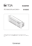
programmable logic development system 10 that includes a
FIG. 1 is a block diagram of a programmable logic
development system according to one embodiment of the
present invention.
FIG. 1 is a block diagram of an embodiment of a
65
computer netWork 12, a programming unit 14 and a pro
grammable logic device 16 that is to be programmed.
Computer netWork 12 includes any number of computers