1
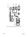
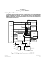
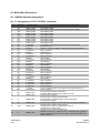
Bit
Name
0
EARB
1
IP
2
BDRV
3
BDIS
4:5
BPS
9:10
DBGC
11
DBPC
12
ATWC
13:14
EBDF
16
PRPM
17:18
SC
19
ETRE
20
FLEN
23
CLES
28:30
ISB
31
DME
Description
0: internal arbitration
1: external arbitration
Interrupt table location after reset
0: MSR(IP) =1
1: MSR(IP) =0
0: reduced drive strength of bus pins
1: full drive strength of bus pins
0: bank 0 is bootable
1: memory controller inactive
Boot port size
00: 32-bit
01: 8-bit
10: 16-bit
11: reserved
Debug pin configuration (IWP,BI,BG,BR,BB)
(6.13.1.1)
Debug pin configuration
0: BDM
1: JTAG
Address type <> Write enable
0: /WE
1: AT
External bus division factor
00: CLKOUT = GCLK2
01: CLKOUT = GCLK2/2
Peripheral mode enable
0: normal
1: external master
Single chip select
00: extended chip, 32-bit data
01: extended chip, 16-bit data
10: single chip, show cycle (address)
11: single chip
Extended table relocation
0: off
1: on
0: internal flash disabled (boot external)
1: internal flash enabled
0: little endian swap logic inactive
1: little endian swap logic active
Initial internal space base (6.12.1.2)
0: dual mapping disabled
1: dual mapping enabled
Var. 1
0
0
1
0
00
10
0
0
00
0
00
0
1
0
00
0
Table 4-1 Hard reset configuration word
MOTOROLA
4-20
EVB555
Quick Reference