1
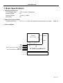
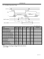
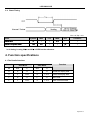
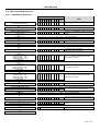
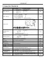
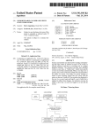
LCD12864-COG
LCD Module User Manual
Rev.
01
Descriptions
Prelimiay Release
Date
2008-08-07
LCD12864-COG
Table of Content
1. Bsaic Specifications……………….………………………………………………3
Display Specifications………………………..……………………………………………………………….3
1.2 Mechanical Specifications………………..…………………………………………………………………..3
1.3 Circuit Diagram…..………………………..…………………………………………………………………..3
1.4 Terminal Function…..…………………..……………………………………………………………………..4
1.1
2. Absolute Maximum Ratings...…….………………………………………………5
3. Electrical Characteristics………….………………………………………………5
3.1
3.2
3.3
3.4
DC Characteristics……..………………..…………………………………………………………………….5
LED Backlight Circuit.(NC)……………..…………………………………………………………………….5
AC Characteristics.…….…………………..………………………………………………………………….6
Reset Timing…………….………………..……………………………………………………………………8
4. Function specifications……………………………………………………………8
4.1
4.2
4.3
4.4
4.5
4.6
The Parallel Interface…………………….……………………………………………………………………8
Basic Setting……………………………….…………………………………………………………………..9
Resetting the LCD module………………….…………………………………….…………………………..9
Display Memory Map………………………………….………………………….……………………………9
Display Commands…………..…………………….…………………………….…………………………..10
Basic Operating Sequence…………...………………………….……………….………………………….11
5. Inspection Standards………………….……………………….………………….12
6. Handling Precautions………..…………………………………….………………13
6.1
6.2
6.3
6.4
6.5
6.6
6.7
Mounting method………………………………………………………….……….………………………….13
Cautions of LCD handling and cleaning……………………………………….….………………………...13
Caution against static charge……………………………………….…………….………………………….13
Packaging……………………………………………………….…………………….………………………..13
Caution for operation…………………………….……………………………….……………………………13
Storage…………………………………………….…………………………….………………………………13
Safety…………………………………………….……………………………….……………………………..13
Page 2 of 14
LCD12864-COG
1. Bsaic Specifications
1.1 Display Specifications
1>LCD Display Mode
2>Viewing Angle
3>Driving Method
4>Backlight
: FSTN, Positive, Transflective
: 6H
: 1/64 Duty, 1/9 Bias
: NC
1.2 Mechanical Specifications
1>Outline Dimension
: 39.5 x 31.1 x 2.0mm (See attached Outline Drawing for Details
PAGE14)
1.3 Circuit Diagram
COM63
LCD Panel
……
128 x 64 Pixels
……
SEG127
VDD
VSS
V0~V4
CAP2-,CAP2+,CAP1+,CAP1-,CAP3+
DB0~DB7
C86,VOUT,/RD,/WR,A0,/RES,/CS1
SEG0
COM0
ST7565R Cortrol/Driver IC
Page 3 of 14
LCD12864-COG
1.4 Terminal Function
Pin No.
Pin Name
Function
28
VDD
27
P/S
26
C86
21~25
V0,V1,V2,V3,V4
16-20
C2-,C2+,C1+,C1-,C3+
15
VOUT
14
VSS
6-13
D0-D7
5
/RD
Read (/RD ) control signal input.
4
/WR
Write (/WR ) control signal input.
3
A0
2
/RES
Reset
1
/CS1
chip selection input
Power supply voltage (Positive)
MPU interface selection pin
LCD driving voltages.
When internal DC-DC voltage converter is used, external
capacitor is connected between these pins.
positive voltage supply pin of the chip.
Negative power supply,0V
8bit Date bus
Data/Command control
Page 4 of 14
LCD12864-COG
2. Absolute Maximum Ratings
Items
Symbol
MIN.
MAX.
Unit
Condition
Supply Voltage
VDD
-0.3
+3.3
V
VSS = 0V
Input Voltage
VIN
-0.3
VDD+0.3
V
VSS = 0V
Operating Temperature
TOP
-10
+60
℃
No Condensation
Storage Temperature
Tst
-20
+70
℃
No Condensation
3. Electrical Characteristics
3.1
DC Characteristics
Vss = 0V,Top = 25℃
Items
Symbol
MIN.
TYP.
MAX.
Unit
Operating Voltage
VDD
2.8
3.0
3.3
V
VDD
Input High Voltage
VIH
0.8 x VDD
-
VDD
V
Input Low Voltage
VIL
VSS
-
0.2 x VDD
V
/CS1,/RES,A0,/WR,
/RD,D0~D7,C86
Output High Voltage
VOH
0.8 x VDD
-
VDD
V
D0~D7
Output Low Voltage
VOL
VSS
-
0.2 x VDD
V
D0~D7
Input Leakage Current
ILI
-1.0
-
1.0
µA
VDD
Output Leakage Current
ILo
-3.0
-
3.0
µA
VDD
3.3
Condition
AC Characteristics
3.3.1 8080 Mode System Bus Timing
Vss = 0V,Top = 25℃
Page 5 of 14
LCD12864-COG
Items
Symbol
MIN.
TYP.
MAX.
Unit
Condition
System cycle time
Tcyc8
500
-
-
ns
-
Address setup time(A0)
Taw8
10
-
-
ns
-
Address hold time(A0)
Tah8
10
-
-
ns
-
Control Low Pulse wide(/RD)
tcclr
275
-
-
ns
-
Control Low Pulse wide(/WR)
tcclw
275
-
-
ns
-
Control High Pulse wide(/RD)
tcchr
225
-
-
ns
-
Control High Pulse wide(/WR)
tcchw
225
-
-
ns
-
Data steup time
Tds8
50
-
-
ns
-
Data hold time
Tdh8
10
-
-
ns
-
/RD access time(*a)
Tacc8
-
-
200
ns
-
Output disable time(*a)
Tch8
15
-
150
ns
-
Note:
*a. all timing is using 20﹪ and 80﹪ of VDD as the reference.
Page 6 of 14
LCD12864-COG
3.3.2
6800 Mode System Bus Timing
Vss = 0V,Top = 25℃
Items
Symbol
MIN.
TYP.
MAX.
Unit
Condition
System cycle time
Tcyc6
500
-
-
ns
-
Address setup time(A0)
Taw6
10
-
-
ns
-
Address hold time(A0)
Tah6
10
-
-
ns
-
Control Low Pulse wide(/RD)
tcclr
275
-
-
ns
-
Control Low Pulse wide(/WR)
tcclw
275
-
-
ns
-
Control High Pulse wide(/RD)
tcchr
225
-
-
ns
-
Control High Pulse wide(/WR)
tcchw
225
-
-
ns
-
Data steup time
Tds6
50
-
-
ns
-
Data hold time
Tdh6
10
-
-
ns
-
/RD access time(*a)
Tacc6
-
-
200
ns
-
Output disable time(*a)
Tch6
15
-
150
ns
-
Note:
*a. all timing is using 20﹪ and 80﹪ of VDD as the reference.
*b. CL = 100pF
Page 7 of 14
LCD12864-COG
3.4
Reset Timing
Vss = 0V,Top = 25℃
Items
Reset time
Reset Low pules width
Symbol
MIN.
TYP.
MAX.
Unit
Condition
Tr
-
-
2.5
µS
-
Trw
2.5
-
-
µS
-
Note:
*a. all timing is using 20﹪ and 80﹪ of VDD as the reference.
4. Function specifications
4.1 The Parallel Interface
Shared
6800 Mode
8080 Mode
Function
A0
R/W
E
/RW
H
H
H
H
L
H
Reads the display data
H
L
HÆL
H
LÆH
Writes the display data
L
H
H
L
H
L
L
HÆL
H
LÆH
Staus read
Write Command data
Page 8 of 14
LCD12864-COG
4.2 Basic Setting
To drive the LCD module correctly and provide normally display, please use the following seting
1> ADC = 0 (normal)
2> SHL select = 1(reverse)
3> LCD Bias Select = 1/9
4> Initial Display Line = 0
5> Entire Display ON/OF = OFF(normal)
6> Reverse Display ON/OF = OFF(normal)
7> Set Power Control Set:
Voltage follower = ON,voltage converter = ON,Voltage regulator = ON
8> Display ON/OF =ON
4.3
Resetting the LCD module
The LCD module should be initialized bu using /RES terminal.
While turning on the VDD and VSS power supply, maintain /RES terminal at LOW level, After the
Power supply stabilized, release the reset terminal(/RES = High)
4.4
Display Memory Map
Page 9 of 14
LCD12864-COG
4.5
Display Commands
Code
D6
D5
D4
D3
D2
D1
Display ON/OFF
0
1
0
1 0
1
0
1
1
1
2
Display start line set
0
1
0
0 1
Display start address
Set the display RAM display start line address
3
Set Page Address
0
1
0
1 0
1
1
Page address
Set the display RAM Page address
0
1
0
0 0
0
1
Col. Add
Set the upper-4-bit of column address counter
4
Ser Column Address
(Upper-4 bits)
Ser Column Address
(Lower-4 bits)
0
1
0
0 0
0
0
Col. Add
Set the low-4-bit of column address counter
0
1
6
Write Display Data
1
1
0
Write Data
Write data into the display RAM
7
Read Display Data
1
0
1
Read Data
Read data from the display RAM
8
ADC Select
0
1
0
1 0
1
0
0
0
0
ADC
Set the display RAM address SEG output
Correspondence
ADC = 0,Normal. ADC = 1,Reverse
9
Normal/Reverse Display
0
1
0
1 0
1
0
0
1
1
REV
REV = 0, Normal
REV = 1, Reverse
10
Entire Display ON/OFF
0
1
0
1 0
1
0
0
1
0
EON
EON = 0, Normal
EON = 1, Entire display ON
11
Set LCD Bias
0
1
0
1 0
1
0
0
0
1
BIAS
0
0
DON
0
0
Bias = 0, 1/9 Bias
Bias = 1, 1/7 Bias
12
Set Read-Modify-Write
0
1
0
1 1
1
0
0
0
0
0
Enter the “Read-Modify-Write” mode
13
Reset Read-Modify-Write
0
1
0
1 1
1
0
1
1
1
0
Clear the “Read-Modify-Write” mode
14
Reset
0
1
0
1 1
1
0
0
0
1
0
15
SHL S elect
0
1
0
1 1
0
0
*
*
*
Resets the LCD module
Set the COM scanning direction
SHL = 0, Normal
SHL = 1, Flipped in y-direction
* = don’t care terms
VF
Read Staus
VR
5
VC
0
DON=0,display off
DON=1,display on
SHL
Status
D0
/WR
1
D7
/RD
Instrctions
A0
No.
Function
Read the status data
Set the power circuit operation mode
VF : LCD Supply Voltage Follower
VR : LCD Supply Voltage Regulator
VF : LCD Supply Voltage Converter
(1 = ON, 0 = OFF)
16
Power Control Set
0
1
0
0 0
1
0
1
17
Regulator Resistor Select
0
1
0
0 0
1
0
0
Electronic volume mode set
0
1
0
1 0
0
Electronic volume register set
0
1
0
*
*
-
-
-
-
-
-
-
-
-
-
Compound instruction
Display OFF + Entire Display ON
1
0
1 1
1
0
0
0
1
1
Non-operation command
18
19
Power Save
20
NOP
0
Ratio
Set the built-in resistor ratio (Rb/Ra)
0 0 0 0 1
Electronic
Control value
Set reference voltage mode
Set reference voltage register
Note:
*a. For the details of the Display Commands, please refer to ST7565R data sheet
Page 10 of 14
LCD12864-COG
4.6 Basic Operating Sequence
4.6.1 Initialization Sequence
Turn on Power Supply VDD & VSS While
maintaining /RES at LOW
D1
D0
A0
D7
D6
D5
D4
D3
D2
Code Function
Note
hex
-
-
-
-
-
-
-
-
-
-
-
-
-
-
-
-
-
-
-
-
-
-
Release the /RES Reset Signal
(/RES = High)
-
-
-
-
-
-
-
-
-
-
See AC Characteristics section for timing
details
LCD Bias = 1/9
0
1
0
1
0
0
0
1
0
A2H
LCD Characteristics
ADC = Normal
0
1
0
1
0
0
0
0
0
A0H
No flip on x-direction (SEG)
SHL = Reverse
0
1
1
0
0
1
0
0
0
C8H
Flip on y- direction (COM)
Initial Display Line = 0
0
0
1
0
0
0
0
0
0
40H
i.e. Display RAM “Page 0-D0”
Matched to top line of the LCD
0
0
0
1
0
1
1
0
0
2CH
Turn on the internal Voltage Converter and
wait until VOUT stable
-
-
-
-
-
-
-
-
-
-
0
0
0
1
0
1
1
1
0
2EH
-
-
-
-
-
-
-
-
-
-
0
0
0
1
0
1
1
1
1
2FH
-
-
-
-
-
-
-
-
-
-
Regulator Resistor Select
0
0
0
1
0
0
1
0
1
25H
Set the built-in resistor ratio to middle
Set Reference Voltage Mode
Set Reference Voltage Resistor
0
0
1
0
0
0
0
1
0
0
0
0
0
0
0
0
1
0
81H
20H
Set to the middle of the range it may be adjused
For achieving the best display contrast
Display ON
0
1
0
1
0
1
1
1
1
AFH
Turn on the LCD display
Set Page Address = 0
0
1
0
1
1
0
0
0
0
B0H
Specify the display data RAM page address to
00H
Set Column Address (Upper -4bit = 0)
Set Column Address (Lower-4bit =4)
0
0
0
0
0
0
0
0
1
0
0
0
0
1
0
0
0
0
10H
04H
Specify the display data RAM column address
to 00H
Write Display Data
1
Wait until power supply is stabilized
Power Control
Voltage Follower = OFF
Voltage Regulator = OFF
Voltage Converter = ON
Delay 50ms
Power Control
Voltage Follower = OFF
Voltage Regulator = OFF
Voltage Converter = ON
Delay 50ms
Power Control
Voltage Follower = OFF
Voltage Regulator = OFF
Voltage Converter = ON
Delay 50ms
Display Data
Turn on the internal Voltage Regulator and
wait until VOUT stable
Turn on the internal Voltage Follower and
wait until VOUT stable
-
Write Other Display Data
Page 11 of 14
LCD12864-COG
5. Inspection Standards
Item
Criterion for defects
(1) Non display
(2) Vertical line is deficient
(3) Horizontal line is deficient (4) Cross line is deficient
Size Φ(mm)
Acceptable number
Φ≤0.3
Ignore (note)
0.3<Φ≤0.45
3
0.45<Φ≤0.6
1
0.6<Φ
0
Length (mm) Width (mm)
Acceptable number
L≤10
W≤0.03
Ignore
5.0≤L≤10 0.03<W≤0.04
3
5.0≤L≤10 0.04<W≤0.05
2
1.0≤L≤10 0.05<W≤0.06
2
1.0≤L≤10 0.06<W≤0.08
1
L≤10 0.08<W
follows 2) point defect
Defects separate with each other at an interval of more than 20mm
1) Display on inspection
2) Black/White spot
3) Black/White line
Major
Minor
Minor
Minor
4) Display pattern
5) Spot-like contrast
irregularity
6) Bubbles in polarizer
7) Scratches and dent on the
polarizer
8) Stains on the surface of
LCD panel
9) Rainbow color
10) Viewing area
encroachment
11) Bezel appearance
12) Defect of land
contact
Defect type
surface
13) Parts mounting
14) Part alignment
15) Conductive foreign
matter (solder ball,
solder hips)
16) Bezel flaw
17) Indication on name plate
(sampling indication label)
A+B≤0.28 0<C D+E≤0.25 F+G≤0.25
2
2
2
Note: 1) Up to 3 damages acceptable
2) Not allowed if there are two or more pinholes every three-fourth inch.
Size Φ(mm)
Acceptable Number
Φ≤0.7
Ignore (note)
0.7<Φ≤1.0
3
1.0<Φ≤1.5
1
1.5<Φ
0
Note: 1) Conformed to limit samples.
2) Intervals of defects are more than 30mm.
Size Φ(mm)
Acceptable Number
Φ≤0.4
Ignore (note)
0.4<Φ≤0.65
2
0.65<Φ≤1.2
1
1.2<Φ
0
Scratches and dent on the polarizer shall be in the accordance with “2)
Black/white spot”, and “3) Black/White line”.
Stains which cannot be removed even when wiped lightly
with a soft cloth or similar cleaning.
No rainbow color is allowed in the optimum contrast on state within the active
area.
Polarizer edge or line is visible in the opening viewing area due to polarizer
shortness or sealing line.
Rust and deep damages that are visible in the bezel are rejected.
Minor
Evident crevices that are visible are rejected.
Minor
(1)
(2)
(3)
(1)
(2)
(1)
(2)
(3)
Failure to mount parts
Parts not in the specifications are mounted
For example: Polarity is reversed, HSC or TCP falls off.
LSI, IC lead width is more than 50% beyond pad outline.
More than 50% of LSI, IC leads is off the pad outline.
0.45<Φ, N≥1
0.3<Φ≤0.45, N≥1, Φ: Average diameter of solder ball (unit: mm)
0.5<L, N≥1, L: Average length of solder chip (unit: mm)
Bezel claw missing or not bent
(1) Failure to stamp or label error, or not legible.(all acceptable if legible)
(2) The separation is more than 1/3 for indication discoloration, in which the
characters can be checked.
Minor
Minor
Minor
Minor
Minor
Minor
Minor
Minor
Minor
Minor
Minor
Page 12 of 14
LCD12864-COG
6. Handling Precautions
6.1 Mounting method
A panel of LCD module made by our company consists of two thin glass plates with polarizers that easily get damaged.
And since the module in so constructed as to be fixed by utilizing fitting holes in the printed circuit board (PCB), extreme care
should be used when handling the LCD modules.
6.2
Cautions of LCD handling and cleaning
When cleaning the display surface, use soft cloth with solvent (recommended below) and wipe lightly.
-Isopropyl alcohol
-Ethyl alcohol
-Trichlorotriflorothane
Do not wipe the display surface with dry or hard materials that will damage the polarizer surface.
Do not use the following solvent:
-Water
-Ketene
-Aromatics
6.3 Caution against static charge
The LCD module use C-MOS LSI drivers. So we recommend you:
Connect any unused input terminal to Vdd or Vss. Do not input any signals before power is turned on, and ground your body,
work/assembly areas, assembly equipment to protect against static electricity.
6.4
Packaging
-Module employs LCD elements, and must be treated as such. Avoid intense shock and falls from a height.
-To prevent modules from degradation, do not operate or store them exposed direct to sunshine or high temperature/humidity.
6.5 Caution for operation
-It is an indispensable condition to drive LCD module within the limits of the specified voltage since the higher voltage over the
limits may cause the shorter life of LCD module.
-An electrochemical reaction due to DC (direct current) causes LCD undesirable deterioration so that the uses of DC (direct
current) drive should be avoided.
-Response time will be extremely delayed at lower temperature than the operating temperature range and on the other hand at
higher temperature LCD module may show dark color in them. However those phenomena do not mean malfunction or out of
order of LCD module, which will come back in the specified operating temperature.
6.6 Storage
In the case of storing for a long period of time, the following ways are recommended:
-Storage in polyethylene bag with the opening sealed so as not to enter fresh air outside in it. And with not desiccant.
-Placing in a dark place where neither exposure to direct sunlight nor light is. Keeping the storage temperature range.
-Storing with no touch on polarizer surface by any thing else.
6.7 Safety
-It is recommendable to crash damaged or unnecessary LCD into pieces and to wash off liquid crystal by either of solvents
such as acetone and ethanol, which should be burned up later.
-When any liquid leaked out of a damaged glass cell comes in contact with your hands, please wash it off well at once with
soap and water.
Page 13 of 14
LCD12864-COG
Page 14 of 14