1
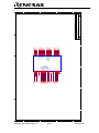
Powerful Processors – Easy to Use™
QSK26A Quick
Start Kit
User’s Manual
Rev. 1.0
January 2006
www.renesas.com
Table of Contents
1.0 Introduction ............................................................................................................................................. 3
2.0 Contents of Product Package................................................................................................................. 4
2.1. QSK26A Quick Start Kit Item List ...................................................................................................... 4
2.1.1. CD-ROM...................................................................................................................................... 4
3.0 Limited Guarantee and Support ............................................................................................................. 5
4.0 System Connectivity ............................................................................................................................... 6
4.1. Host Computer Requirements ........................................................................................................... 7
4.2. QSK26A Board .................................................................................................................................. 7
4.3. Software Development Tools ............................................................................................................ 7
4.3.1. HEW (High-performance Embedded Workshop)........................................................................ 7
4.3.2. NC30WA Evaluation Version C Compiler ................................................................................... 7
4.3.3. HEW Debug Interface ................................................................................................................. 7
4.3.4. FoUSB (Flash-over-USB™) Programmer ................................................................................... 7
5.0 Hardware ................................................................................................................................................ 8
5.1. QSK26A Board .................................................................................................................................. 8
5.2. QSK26A Board Block Diagram.......................................................................................................... 9
5.3. M16C/26A Group of MCUs................................................................................................................ 9
5.4. QSK26A Board Jumper Configuration............................................................................................. 10
5.4.1. JP1: MCU (U4) Power............................................................................................................... 10
5.4.2. Default Jumper Settings ............................................................................................................ 10
5.5. LCD (Liquid Crystal Display) ........................................................................................................... 10
6.0 System Operation & Limitations ........................................................................................................... 11
6.1. Kernel (ROM Monitor) Introduction.................................................................................................. 11
6.2. Pin and Peripheral Limitations......................................................................................................... 11
6.3. Memory Map.................................................................................................................................... 12
6.4. Register Operation Limitations ........................................................................................................ 12
6.5. Limitations on Interrupts - Vectors that Reside in the Hardware Vector Table ............................... 13
6.6. Stop or Wait Mode Limitations......................................................................................................... 13
6.7. User Program’s Real-Time Capability (Very Important – Please Read) ......................................... 13
6.8. Performing Debug Using Symbols .................................................................................................. 13
7.0 QSK26A Board Specifications.............................................................................................................. 15
7.1. Hardware Specifications.................................................................................................................. 15
7.2. QSK26A Power & Run LED Status ................................................................................................. 15
7.3. Power Supply Requirements ........................................................................................................... 15
7.4. Operating Environment.................................................................................................................... 16
Appendix A. Troubleshooting Guide........................................................................................................... 17
A.1 Manual Installation ........................................................................................................................... 17
A.2 USB Driver Problems ....................................................................................................................... 17
A.3 Debugging Problems........................................................................................................................ 18
A.3.1 Erratic Debug Behavior.............................................................................................................. 18
A.3.2 Can’t Connect to Target............................................................................................................. 18
A.3.3 Can’t Debug in HEW.................................................................................................................. 19
A.3.4 Issues that May Arise During Debug Operations ...................................................................... 19
Appendix B. Updating the QSK26A Board’s In-Circuit Debugger & Programmer Firmware .................... 21
Appendix C. Reference Manuals................................................................................................................ 23
Appendix D. Expansion Headers................................................................................................................ 24
Appendix E. QSK26A Printed Circuit Board............................................................................................... 31
Appendix F. Other Resources .................................................................................................................... 33
QSK26A User’s Manual Rev 1.0
January 2006
1.0 Introduction
The QSK26A Quick Start Kit (QSK) is a low-cost development environment for evaluating M16C/26A
group microcontrollers (MCU) and Renesas software development tools.
The kit comes with a complete software development tool chain for Renesas MCUs, including Highperformance Embedded Workshop (HEW), which includes Integrated Development Environment (IDE),
Graphical User Interface (GUI) and Software Debugger; NC30WA C-compiler, assembler and linker; and
Flash-over-USB™ (FoUSB) Programming software.
The QSK26A board features on-board in-circuit debugging and programming support (ICD), eliminating
the need for an external ICD unit. All that is required for in-circuit debugging and programming with the
QSK26A is a USB connection to a PC and the included development tool software.
A real-time, source-level debug environment is implemented using the HEW4 software debug interface in
conjunction with the QSK26A board. The Flash-over-USB™ (FoUSB) Programmer software allows insystem programming of the QSK26A board’s M16C/26A Flash MCU.
QSK26A User’s Manual Rev 1.0
3/ 33
January 2006
2.0 Contents of Product Package
This section describes the contents of the QSK26A product package. When unpacking your QSK26A,
please check to see that all items listed below are included.
2.1. QSK26A Quick Start Kit Item List
Table 2-1 lists the items included in the QSK26A.
Table 2-1 QSK26A Item List
Item Name
QSK26A Board
6’ Mini USB Cable
CD-ROM
Quantity
1
1
1
Remarks
M16C/26A QSK Board with integrated in-circuit
debugging and programming support
Connects QSK26A board to Host PC
Auto-install program
HEW (IDE & debugger)
NC30WA (C-compiler, assembler, and linker)
FoUSB Programmer
USB drivers
Manuals
Tutorials
Sample programs
2.1.1. CD-ROM
The CD-ROM contains the electronic manuals and software necessary for developing programs. Your
computer must have a web browser — like Mozilla Firefox, Netscape® Browser or Microsoft® Internet
Explorer — to view the help files, and Adobe® Acrobat® Reader® to view the manuals.
Insert the enclosed CD into your computer and the installer should auto-start. The installer program
will create C:\Renesas and C:\Workspace folders on your machine. NC30WA, FoUSB
Programmer, Documentation, sample code, and other QSK-related files are in the C:\Renesas
folder. HEW is installed in the C:\Program Files\Renesas folder by default.
If the installer program does not start, browse to the CD’s root folder and double-click on
QSK-installer.exe to start the installation.
QSK26A User’s Manual Rev 1.0
4/ 33
January 2006
3.0 Limited Guarantee and Support
Renesas Technology America, Inc., warrants the QSK26A to be free from component or assembly
defects for a period of 180 days from the date of purchase. Settlement is limited to repair or replacement
of the product only. Renesas Technology America, Inc., does not assume any liability arising out of the
application or use of any product, circuit or procedure described herein. No other liability or warranty
applies, expressed or implied. Software warranty is limited to replacement of the CD only. While every
attempt has been made to ensure accurate documentation, Renesas Technology America, Inc., cannot
be held responsible for errors or omissions, and reserves the right to make changes without prior notice.
“Flash-over-USB” is a trademark of Renesas Technology America, Inc. All other trademarks are the
properties of their respective owners.
Support for the QSK26A kit is provided via the following channels only:
1. Online User Forums at www.renesasunivsersity.com
2. Digikey Technical Support: www.digikey.com, click the “Contact Us” link
3. Renesas Technical Support Center, email at [email protected]
QSK26A User’s Manual Rev 1.0
5/ 33
January 2006
4.0 System Connectivity
The following lists the hardware and software products required for using the QSK26A Quick Start Kit.
•
•
•
•
Host Computer (supplied by user)
QSK26A Board
Mini USB cable
Software Tools (HEW IDE, NC30 Compiler/Linker, FoUSB Programmer)
Figure 4-1: QSK26A System Connectivity
QSK26A User’s Manual Rev 1.0
6/ 33
January 2006
4.1. Host Computer Requirements
The minimum requirement to be able to use the software that comes with the QSK26A is a PC with a
USB port and Microsoft Windows 98, Me, 2000, or XP.
4.2. QSK26A Board
The QSK26A board provides an evaluation and development environment for the M16C/26A group
MCUs. See section “5.0 Hardware” for more details.
4.3. Software Development Tools
The installer program installs all the development tools. For details on installation, see the QuickStart
Guide or instructions in Appendix A of this manual. A brief description of all the included tools follows.
Please refer to the individual tool manuals for detailed information.
4.3.1. HEW (High-performance Embedded Workshop)
HEW provides a Graphical User Interface (GUI) that integrates the software development tools and
includes the C-compiler, assembler, linker, debugger and editor.
4.3.2. NC30WA Evaluation Version C Compiler
The evaluation version of the M3T-NC30WA C-compiler is provided with the same functionality as the
commercial version except that link size will be restricted to 64 kBytes after 60 days from when you
begin using the compiler. Contact your local sales representative if you wish to purchase a full license.
4.3.3. HEW Debug Interface
HEW communicates with a kernel (i.e. a ROM monitor program) on the target MCU through the ICD.
This debug interface provides a highly efficient evaluation environment. Features include:
•
•
•
•
•
Source-level debugging for assembly and C language
Single-step command (unlimited breakpoints)
Run command with 6 breakpoints* for the M16C/26A
RAM monitor function
C variable “watch” window
*Note: The number of breakpoints will vary depending on the M16C Flash MCU used.
4.3.4. FoUSB (Flash-over-USB™) Programmer
The Flash-over-USB Programmer application provides In-System Programming capability for the
starter kit or any target board using an M16C family Flash MCU (e.g. R8C, M16C, M32C). Please see
the RTA-FoUSB-MON User’s Manual for more details.
QSK26A User’s Manual Rev 1.0
7/ 33
January 2006
5.0 Hardware
5.1. QSK26A Board
Figure 5-1 shows the QSK26A Board with major components identified.
Figure 5-1: QSK26A Board
QSK26A User’s Manual Rev 1.0
8/ 33
January 2006
5.2. QSK26A Board Block Diagram
The QSK26A board incorporates an M30260F8AGP (48-pin QFP) from the M16C/26A group of
microcontrollers, designated as IC101. Figure 5-2 shows the QSK26A block diagram.
Figure 5-2: QSK26A Block Diagram
5.3. M16C/26A Group of MCUs
The M16C/26A group of 16-bit single-chip Flash microcontrollers (MCU) is part of the M16C/Tiny family
and utilizes an M16C/60 series CPU core. The hardware and software manuals for the M16C/26A group
of microcontrollers can be found in the C:\Renesas\QSK26A\Docs folder on your PC or from the Start
menu (Start > Programs > Renesas > QSK26A > Document Descriptions) after QSK software installation.
QSK26A User’s Manual Rev 1.0
9/ 33
January 2006
5.4. QSK26A Board Jumper Configuration
5.4.1. JP1: MCU (U4) Power
5.4.2. Default Jumper Settings
Table 5-1: Default Jumper Settings
Jumper
JP102: MCU Power Measurement
JP103: Oscillator Stop Detection
Default
Setting
Open*
Open*
* Both JP102 and JP103 are unpopulated and bypassed by 0Ω resistors. If the 0Ω resistors are
removed and jumpers installed, the default setting for both jumpers would be “closed”.
Referring to the schematics in Appendix E, you can see that jumper JP102 is bypassed by R122, a
0Ω resistor. To measure the MCU current, you need to remove R122, install a jumper header in
location JP102 and measure the current into the MCU by hooking up a multi-meter (in DC current
mode) between the two header contacts. After measurement, place a jumper over the two contacts.
JP103 is bypassed also by a 0Ω resistor: R131. By removing R131, then installing a jumper header in
location JP103 and placing a jumper over the header, the MCU oscillator works normally. Removing
the jumper will stop the oscillator. This can be used to test the MCU’s integrated Oscillator Stop
Detection feature.
5.5. LCD (Liquid Crystal Display)
The LCD is a 2-line by 8-character display with a KS0066 controller IC.
QSK26A User’s Manual Rev 1.0
10/ 33
January 2006
6.0 System Operation & Limitations
The QSK26A provides sophisticated on-board debugging features at a low cost. The QSK26A’s in-circuit
debugging and programming circuitry (ICD) cannot be disconnected for use with other M16C based
boards. For M16C boards without on-board debugging/programming circuitry, Renesas offers the
functionally equivalent, standalone RTA-FoUSB-MON in-circuit debugger/programmer. You can find
detailed information on the RTA-FoUSB-MON and its functionality in the RTA-FoUSB-MON user’s manual.
The QSK26A does have some limitations when used with the HEW software debugger and the board’s
ICD circuit. Section 6.1 introduces the kernel (ROM monitor) program and its purpose. The limitations
when this kernel is running with the user program are listed in Table 6-1.
Table 6-1: System Limitations when Debugging
Item
Please Refer To
6.2 Pin and Peripheral Limitations
6.3 Memory Map
User Limitations
6.4 Register Operation Limitations
6.5 Limitations on Interrupts - Vectors that Reside in the Hardware
Vector Table
6.6 Stop or Wait Mode Limitations
The kernel cannot be run in STOP or WAIT modes. Do not use these
Debugger Limitations
modes when debugging your program
6.7 User Program’s Real-Time Capability
6.1. Kernel (ROM Monitor) Introduction
During debug, a small program called a kernel is uploaded to the M16C/26A (M30260F8AGP) MCU. The
kernel communicates with HEW through the ICD portion of the QSK26A board regarding MCU status
during user code debugging operations.
There are no special steps required in the user program to make use of the ICD portion. The operation of
the kernel is transparent to the user, but there are some limitations. These are discussed from section 6.2
onward.
After starting a HEW debug session, the ICD uploads the kernel to the M16C/26A if it does not already
exist (e.g. on a blank device or a device that was programmed with the FoUSB Programmer). After
downloading the kernel, the M16C/26A is ready to download user code.
Connecting the QSK26A board without starting HEW will not affect the signal lines connected between
the ICD MCU (M37641F8) and the M16C/26A; the ICD MCU keeps the signal lines in high-impedance
state. The ICD MCU only drives the pins after HEW or the FoUSB Programmer attempts to connect.
After completing program debug and verification with HEW, you can create an image of your code in Intel
(.hex) or Motorola (.mot) file formats. This image can be programmed into the M16C/26A using the
FoUSB Programmer. This procedure erases the kernel and leaves only the user program.
6.2. Pin and Peripheral Limitations
SIO/UART1 pins are used for communication between the M16C/26A kernel on the QSK26A board and
the board’s ICD MCU (M37641F8). Do not connect these pins to any other circuit, as SIO/UART1 cannot
be used in the user program while using the Debugger.
QSK26A User’s Manual Rev 1.0
11/ 33
January 2006
6.3. Memory Map
The amount and locations of memory used by the kernel on the QSK26A board’s M16C/26A MCU are
shown in Figure 6-1.
Figure 6-1: M30260F8AGP Memory Map with the Kernel Program
Note: The kernel occupies memory associated with special-page vector numbers 18-19 and 192-255. The
user reset vector is re-mapped to address FFFD8h by the kernel.
6.4. Register Operation Limitations
Table 6-2 lists the limitations on register operation. The registers are inhibited from any modification. If
register contents are modified in any way, kernel operation cannot be guaranteed.
Table 6-2: Limitations on Register Operation
Register Name
User and Interrupt Stack Pointers
UART1 Transmit/Receive Mode Register
UART1 Transmit/Receive Control Register 0
UART1 Transmit/Receive Control Register 1
UART1 Interrupt Control Register 0
UART Transmit/Receive Control Register 2
UART1 Transmit Buffer Register
QSK26A User’s Manual Rev 1.0
Restriction
RAM memory range 0B80H – 0BFFH is used by
the kernel. Do not set stacks in this area.
Do not change.
Do not change.
Do not change bits 0 and 2.
Do not write to this register.
12/ 33
January 2006
UART1 Receive Buffer Register
Port 6 and Port 6 DDR
Do not read this register.
To prevent changes on P6_4 data and direction,
use read-modify-write only instructions (BSET,
BCLR, AND, OR, etc.).
6.5. Limitations on Interrupts - Vectors that Reside in the Hardware Vector Table
Table 6-3 lists the limitations on hardware interrupt (i.e. fixed) vector addresses.
Table 6-3: Interrupt Vector Addresses
Interrupt Cause
M16C/26A Vector Address
Undefined
FFFDCh ~ FFFDFh
Overflow
FFFE0h ~ FFFE3h
BRK Instruction
FFFE4h ~ FFFE7h
Address Match
FFFE8h ~ FFFEBh
Single-step
FFFECh ~ FFFEFh
Watchdog Timer
FFFF0h ~ FFFF3h
DBC
FFFF4h ~ FFFF7h
NMI
FFFF8h ~ FFFFBh
RESET
FFFFCh ~ FFFFFh
Kit Specification
User available
User available
User inhibited
User inhibited
User inhibited
User available (Note 1)
User inhibited
User available
Reset vector (Note 2)
NOTES:
(1) The Watchdog Timer vector is shared with the oscillation stop and voltage detection interrupts.
The vector is available for oscillation stop and voltage detection interrupts, but you must avoid using
the vector for watchdog timer interrupts.
(2) The kernel transparently relocates the Reset vector to FFFD8h.
6.6. Stop or Wait Mode Limitations
The kernel cannot be run in STOP or WAIT modes. Do not use these modes when debugging your
program.
6.7. User Program’s Real-Time Capability (Very Important – Please Read)
Please be aware that while the kernel is in a “STOP” state, the hardware peripherals will continue to run.
Therefore, interrupts may not be serviced properly. In addition, the watchdog timer will not be serviced
and will likely time out if active.
While the kernel is in a “RUN” state, there is no overhead on the application code unless a RAM monitor
window is open. This window requires periodic communication with the MCU. This communication
suspends normal application operation while servicing the request (approximately 2000 BCLK cycles for
each 16 Bytes of data displayed in the window are used per window update). The user must determine
whether this behavior is acceptable.
6.8. Performing Debug Using Symbols
Normally when a new project is created using HEW, debugging symbols are enabled. If you are unable to
view the source properly during debug, add the debug option [-g] in HEW before compiling the programs.
To enable the [-g] option, perform the following:
•
•
•
•
Open the workspace and project in HEW.
Select ‘Renesas M16C Standard Toolchain’ from the Options pull-down menu.
Click on the [Link] tab.
Select ‘Output’ under the ‘Category’ list box.
QSK26A User’s Manual Rev 1.0
13/ 33
January 2006
•
•
Click on the checkbox for [-g] ‘Outputs source debug information…’
Click on the <OK> button
For more information, see the HEW user’s manual.
QSK26A User’s Manual Rev 1.0
14/ 33
January 2006
7.0 QSK26A Board Specifications
7.1. Hardware Specifications
Table 7-1 lists the specifications of the QSK26A Board.
Table 7-1: QSK26A Board Specifications
Item
Specification
MCU
M30260F8AGP
Clocks
Main Clock: crystal 10 MHz, PLL, or ring oscillator
Sub Clock: 32.768 kHz crystal
Memory
RAM: 2kB (1920 Bytes user available due to kernel)
High E/W Data Block: 2kB × 2
Flash ROM: 62kB (63,744 Bytes)
Connectors
[J101-J104]: Four 25-pin, single row, measurement test points connected to
the MCU pins. Can also be used to connect your own expansion boards via
2×25 headers.
[J205]: Mini-USB connector, used for in-circuit debugging and programming
Jumpers
Switches
LEDs
LCD
[JP102]: MCU Power for Icc Measurements
[JP103]: Oscillator Stop detection
[S101]: Pushbutton (connected to P8_3)
[S102]: Pushbutton (connected to P8_2)
[S103]: Pushbutton (connected to P8_1)
[S104]: Pushbutton (connected to Reset)
[D101] (Red): Run LED (in-circuit debugging/programming activity)
[D102] (Green): Power
[D103] (Red): User output (connected to P8_0)
[D104] (Yellow): User output (connected to P7_4)
[D105] (Green): User output (connected to P7_2)
2-line × 8-character LCD with KS0066 controller IC
7.2. QSK26A Power & Run LED Status
The green Power LED (D102) and the red Run LED (D101) indicate operating status of the QSK26A
board. The board’s M37641F8HP MCU that controls the In-Circuit Debugging and Programming
functionality of the board also controls both LEDs. For the LEDs to function as per the table below, it is
necessary that the M37641F8HP MCU is programmed with the correct MCU Monitor Image (MMI) for the
QSK26A. Boards shipped from the factory have the correct MMI loaded. In case your board’s MMI ever
gets
corrupted,
see
”Appendix
B
Updating
the
QSK26A
Board’s
In-Circuit Debugger & Programmer Firmware” for help.
QSK26A Status
No Power (USB cable disconnected)
Connected, USB not enumerated (driver not installed)
Connected, USB enumerated
KD30 Software Debugger running
Power LED
(green)
Off
Blinking
On, Solid
On, Solid
Run LED
(red)
Off
Off
Off
On, Solid
7.3. Power Supply Requirements
The QSK26A Board is powered by the USB bus. It will draw about 50mA with no LEDs on.
QSK26A User’s Manual Rev 1.0
15/ 33
January 2006
7.4. Operating Environment
Table 7-2 lists the environmental conditions for using and storing the QSK26A board. Store the board in a
conductive bag inside the original factory packaging.
Table 7-2: Operating and Storage Environments
Environmental Condition
Ambient Temperature
Operating
0 to 55°C
(No corrosive gas allowed)
Storage
-30 to 75°C
(No corrosive gas allowed)
QSK26A User’s Manual Rev 1.0
16/ 33
Ambient Humidity
30 to 80% (non-condensing)
30 to 80% (non-condensing)
January 2006
Appendix A. Troubleshooting Guide
This section discusses possible problems you may encounter while installing the development tool
software, USB drivers, or running the HEW debugger and FoUSB Programmer applications. This section
also discusses the countermeasures and solutions to resolve these problems.
If, for any reason, you cannot resolve the problem, further assistance is available via the following support
channels:
1. Online User Forums at www.renesasunivsersity.com
2. Digikey Technical support: www.digikey.com, click the “Contact Us” link
3. Renesas Technical Support Center, email at [email protected]
A.1 Manual Installation
Before connecting the QSK26A to your PC, the driver files (.inf and .sys) and executables must be copied
to the C:\Renesas\FoUSB directory.
To do this, run FoUSB_Vx.xx.exe in the \Tools\FoUSB directory of the CD. After the FoUSB
Programmer installation, assuming the default directory was used, you should find a
C:\Renesas\FoUSB folder. The Windows USB drivers can be found under the USB Drivers subfolder,
i.e. fousb.inf, fousb.sys (driver files to run FoUSB Programmer), usbmon.inf, and usbmon.sys
(driver files to run HEW).
A.2 USB Driver Problems
This part discusses how to fix common problems that may occur with USB driver installation. The most
common problem is that Windows did not properly install the USB drivers, so the QSK26A is not
recognized. An indication of this problem is the QSK26A’s red Power LED blinking. When the driver is
installed properly, the red Power LED will be on solid.
Before trying the following steps, try restarting your PC to see if this resolves the problem. You can check
the USB Driver status using the Windows Device Manager (Start > Control Panel > System Properties >
Hardware > Device Manager > Universal Serial Bus controllers). If the “Renesas FoUSB ICD” appears
under the Universal Serial Bus controllers with no red X or yellow exclamation point, the driver was
installed properly.
NOTE: If you are using Windows 2000 or XP, you will need Administrator privileges to be able to
install the drivers.
For cases where “Renesas FoUSB ICD” appears with a red X or yellow exclamation point in the Windows
Device Manager, please try the following:
1. Open the Windows Device Manager (Start > Control Panel > System Properties > Hardware >
Device Manager > Universal Serial Bus controllers).
2. Double-click on ‘Renesas FoUSB ICD’. A Renesas FoUSB ICD Properties dialog box appears.
3. Click on the [Driver] tab and click the <Update Driver> button.
4. Select ‘Display a list…’ and click on the <Have Disk> button.
5. Browse to the C:\Renesas\FoUSB\USB Drivers directory and install the usbmon.sys
driver.
6. If this process does not work, please follow the instructions below.
QSK26A User’s Manual Rev 1.0
17/ 33
January 2006
If you encounter problems on installing the drivers, you can try the following:
Windows 2000
a. Copy the fousb.inf and usbmon.inf files from the C:\Renesas\FoUSB\USB
Drivers folder to the \WINNT\INF folder.
b. Copy the fousb.sys and usbmon.sys files from the C:\Renesas\FoUSB\USB
Drivers folder to the \WINNT\SYSTEM32\drivers folder.
Windows 98 or XP
a. Copy the fousb.inf and usbmon.inf files from the C:\Renesas\FoUSB\USB
Drivers folder to the \WINDOWS\INF folder.
b. Copy the fousb.sys and usbmon.sys files from the C:\Renesas\FoUSB\USB
Drivers folder to the \WINDOWS\SYSTEM32\drivers folder.
A.3 Debugging Problems
This section discusses the causes of common problems and countermeasures to resolve them. The
common problems encountered with debugging are:
• Erratic debug behavior
• Can’t connect to target
• Issues that may come up during debug operations
• Can’t debug in HEW
A.3.1 Erratic Debug Behavior
HEW allows you to launch multiple instances of itself. However, if more than one instance of HEW is open
during a debug session, erratic behavior can result. Running the FoUSB Programmer at the same time as
HEW can result in erratic debug behavior also. Furthermore, having more than one QSK26A board or a
Renesas external ICD installed can also cause erratic problems or cause HEW to crash.
A.3.2 Can’t Connect to Target
If the message “Can’t connect with the target” is displayed when attempting to connect, there are several
reasons that may have caused this message to appear. Each cause and its corresponding
countermeasure is discussed below.
•
The QSK26A board is not connected correctly.
Unplug the QSK26A board from the USB cable. Then connect the QSK26A board back to your PC’s
USB port via the supplied mini USB cable. Please see section “4.0 System Connectivity”.
•
The QSK26A board has no power (Power LED of the QSK26A is off).
The QSK26A board’s power is supplied via the USB bus. Check that your USB cable is not broken.
Check that your PC’s USB port is working correctly. If you connect the QSK26A via a USB hub, check
the connectivity between the hub and your PC. If you use a self-powered hub, check the power
supply of your hub.
•
USB was not selected on the HEW Init dialog box.
QSK26A User’s Manual Rev 1.0
18/ 33
January 2006
Please select ‘USB’ from the Init dialog box that is displayed right after you start a debug session.
•
The selected MCU on the ICD board and the actual target MCU (M16C/26A) do not match.
Close the error message by clicking on the <OK> button, then click on the <Cancel> button of the Init
window. Make sure you select ‘M30260F8A.mcu’. If the MCU loaded on the ICD is different, HEW will
re-program the ICD to match it.
•
The target MCU is damaged.
Try a different target board and see if HEW will connect. You may have a damaged board or MCU.
A.3.3 Can’t Debug in HEW
HEW 4.0 is the first version of HEW to integrate the M16C debug interface. If you have inadvertently
installed an older version of HEW, you will need to uninstall it and re-install HEW4.
A.3.4 Issues that May Arise During Debug Operations
While debugging user code, some issues may come up because the limitations discussed in section “6.0
QSK26A User’s Manual Rev 1.0
19/ 33
January 2006
System Operation & Limitations” were not satisfied. The common issues are listed in Table A.3, including
the countermeasures.
Table A.3
Problem
After
stepping
a
few
instructions, HEW cannot
“stop”
Breakpoints do not seem to
work
HEW locks up (cannot stop
program) or Communication
error message is displayed
•
•
•
•
•
•
Download problems
•
Possible Cause/s and Solution
Changes were made to the UART1 Special Function
Registers (SFRs). Do not change UART1 SFRs in your
code.
System is in “FreeRun” mode. Change the RUN mode to
“Sampling” from the “Init” window (Emulator System icon).
Changes were made to the UART1 SFRs. Do not change
UART1 SFRs in your code.
Ensure that no limitations in Section 6 were violated.
Re-initialize the system without closing debug session. See
note below.
Do a hardware reset. User-program runaway may be
corrupting the kernel (RAM, interrupt vectors, flags, etc.).
Close the debug session, hit the reset button on the QSK
board to reset the board, then restart.
HEW project was not set up properly (startup files missing or
out of order, files added to wrong member, etc.). Try
creating a new project and adding your source files to it. For
details, please see the HEW User’s Manual.
To re-initialize the system without closing a debug session, try the following:
•
•
•
•
Click the <OK> button on the error dialog box to close it.
When an Exit dialog box appears, click the <Cancel> button to close it.
Press the reset button on the QSK26A board.
Click the HEW Reset icon.
After initialization, debugging can resume. However, it is recommended that you download your program
again before debugging.
QSK26A User’s Manual Rev 1.0
20/ 33
January 2006
Appendix B. Updating the QSK26A Board’s
In-Circuit Debugger & Programmer Firmware
This section discusses how to update the firmware of the QSK26A board’s M37641F8 MCU, which is
used to implement the board’s in-circuit debugging (ICD) and programming functionality. Under normal
circumstances, you should never have to perform this update, unless the ICD MCU’s memory becomes
accidentally corrupted.
The M37641F8 MCU has a boot mode that can be used to program the MCU’s user Flash area. The
procedure to activate the boot mode to re-program the Flash firmware is described in the following steps.
1. Unplug the QSK26A board unit from the USB cable.
2. Locate the contact labeled “BOOT” on connector J103 and, if not done already, solder a 2-pin,
2.54mm (0.100 mil) jumper header into the “BOOT” and the adjacent “VCC” contact hole to the
right.
3. Shunt the jumper header with a 2.54mm (0.100 mil) jumper, thus connecting the BOOT signal to
Vcc. This will force the M37641F8 MCU to run in boot mode when it is powered up.
Figure 7-1: Boot Jumper Location
4. Plug the USB cable back in. The M37641F8 MCU will now be in boot mode and will communicate
as a USB device to the PC. In boot mode, the M37641F8 MCU uses a different USB Driver than
the In-Circuit Debugger/Programmer application, so you will need to load another USB Driver
when doing this procedure for the first time. The Windows New Hardware Wizard should
automatically start and guide you through the installation of the required USB driver. The driver is
located in C:\Renesas\FOUSB\USB Drivers.
5. Open the Flash-over-USB program. Note that the MCU device name displayed in green on the
front screen will change automatically to M37641F8 without having to select that device.
6. Click on the <Load MMI> button on the right. This opens a chip selection window.
QSK26A User’s Manual Rev 1.0
21/ 33
January 2006
Figure 7-2: Load MMI Button
7. Select the M16C/Tiny Series > M16C/26A Group > M30260F8A part and click the <OK> button to
load the selected MCU Monitor Image (MMI) to the ICD MCU.
Figure 7-3: Chip Selection Window
8. Unplug the USB Cable and remove the jumper connecting the BOOT signal to Vcc. Reconnect
the QSK26A board to your PC with the USB cable.
9. After you connect the QSK26A board back to the PC, the FoUSB Programmer should show the
target MCU device name you selected earlier.
QSK26A User’s Manual Rev 1.0
22/ 33
January 2006
Appendix C. Reference Manuals
Item
Title
Description
QSK26A Quick Start Guide
Document that will help you get started on using the
QSK26A Starter Kit.
2.
3.
QSK26A User’s Manual
QSK26A Board Schematic
3.
5.
7.
QSK26A Board BOM
M16C/20/60 Series C-Language
Programming Manual
M16C/20/60 Series Assembly
Language Programming Manual
HEW User’s Manual
8.
9.
10.
AS30 User’s Manual
NC30 User’s Manual
RTA-FoUSB-MON User’s Manual
This document.
Schematic diagram for the RF Sniffer and QSK
boards.
Bill of materials for the QSK board.
ANSI C-language programming guide for the
M16C/20/60 series MCUs.
Assembly language programming guide for the
M16C/20/60 series MCUs.
Document that describes installation and operation
of this Integrated Development Environment for
Renesas’ Tools.
Guide for AS30 assembler.
Guide for NC30WA C-compiler.
Information
on
in-circuit
debugging
and
programming
1.
6.
NOTE:
The installer will copy all these manuals during installation. They can be viewed using the Document
Descriptions file by clicking on Start > Programs > Renesas > QSK26A > Document Descriptions.
QSK26A User’s Manual Rev 1.0
23/ 33
January 2006
Appendix D. Expansion Headers
The M30260F8AGP MCU on the QSK26A target board is housed in a 48-pin QFP package. Pin 1 of the
package is identified by the number ‘1’ on the board’s top silkscreen. Connectors J101 to J104, located
on the long sides of the board, provide access to almost all of the MCU’s pins. You can use J101 to J104
as test points to check MCU signals or, by mounting your own headers, to connect your own expansion
board. The silkscreen identifying the connectors is at the top of the QSK26A board. The following table
shows the mapping of J101 to J104 pins to MCU pins and signal names.
48
QFP
MCU
Pin
11,47
Vcc
1
2
3
4
5
6
7
8
100
QFP
MCU
Pin
16,
62,99
88
86
84
82
80
78
76
48
QFP
MCU
Pin
9,44
Gnd
2
3
4
5
6
7
8
100
QFP
MCU
Pin
14,
64,96
87
85
83
81
79
77
75
na
na
na
na
na
na
na
P00/D0
P02/ D2
P04/ D4
P06/ D6
P10/ D8
P12/ D10
P14/D12
na
na
na
na
na
na
36
P01/ D1
P03/ D3
P05/ D5
P07/ D7
P11/ D9
P13/ D11
P15/ D13/ INT3
9
74
35
P16/ D14/ INT4
9
73
34
P17/ D15/ INT5
10
11
72
na
P20/A0/ D 0
71
na
P21/ A1/ D1
70
na
P22/ A2/ D 2
10
11
69
na
P23/ A3/ D 3
12
68
na
P24/ A4/ D 4
12
67
na
P25/ A5/ D 5
13
66
na
P26/ A6/ D 6
13
65
na
14
63
na
14
61
na
15
16
17
18
19
20
60
58
56
54
52
50
na
na
na
na
na
na
P30/ A8/ D 8
P32/ A10
P34// A12
P36// A14
P40// A16
P42// A18
P44/ CS 0
P27/ A7/ D 7
P31/ A9
15
16
17
18
19
20
59
57
55
53
51
49
na
na
na
na
na
na
P33// A11
P35// A13
P37// A15
P41// A17
P43// A19
P45/ CS 1
21
48
na
P46/ CS 2
21
47
na
P47/ CS 3
22
23
24
46
44
42
na
na
na
22
23
24
45
43
41
na
na
na
P51/ WRH / BHE
P53/BCLK
25
40
na
P50/ WRL / WR
P52/ RD
P54/ HLDA
P56/ALE
25
39
na
P57/ RDY /CLKOUT
J101
Pin
1
J102
Pin
MCU Function
QSK26A User’s Manual Rev 1.0
24/ 33
MCU Function
P55/ HOLD
January 2006
48
QFP
MCU
Pin
11,47
2
100
QFP
MCU
Pin
16,
62,99
9
Vcc
1
4
CNVss
2
100
QFP
MCU
Pin
14,
64,96
12
3
4
5
97
94
92
45
42
40
P100/AN0
P102/AN2
P104/AN4/ KI0
3
4
5
95
93
91
43
41
39
6
90
38
6
89
37
3
1
na
na
P106/AN6/ KI2
P90/TB0in
P92/TB2in
P94/DA1/TB4in
P96/ANEX1/SOUT4
7
8
9
10
7
5
3
1
7
8
9
10
6
4
2
100
2
48
na
na
P107/AN7/ KI3
P91/TB1in
P93/DA0/TB3in
P95/ANEX0/CLK4
P97/ AD Trg /SIN4
11
22
17
P80/TA4out/U
11
21
16
P81/TA4in/ U
12
20
15
P82/ INT0
12
19
14
P83/ INT1
13
18
13
17
12
14
15
16
na
30
28
6
25
23
P84/ INT2
P86/Xcout
P70/TxD2/SDA/TA0out
P72/CLK2/TA1out/V
13
14
15
16
na
29
27
5
24
22
P85/ NMI / SD
P87/Xcin
P71/RxD2/SCL/TA0in/ TB5in
P73/ CTS 2 / RTS 2 /TA1in
17
18
19
26
24
38
21
19
33
17
18
19
25
23
37
20
18
32
/V
P75/TA2in/ W
P77/TA3in
P61/CLK0
20
21
36
34
31
29
20
21
35
33
30
28
P63/TxD0
P65/CLK1
22
23
24
32
na
16,
62,99
16,
62,99
27
na
11,47
P74/TA2out/W
P76/TA3out
P60/ CTS 0 / RTS 0
P62/RxD0
P64/ CTS1 / RTS1 /
/CLKS1
P66/RxD1
BOOT*
Vcc
22
23
24
26
na
9,44
P67/TxD1
BYTE
Gnd
11,47
Vcc
25
31
8
14,
64,96
14,
64,96
9,44
Gnd
J103
Pin
1
25
J104
Pin
MCU Function
48
QFP
MCU
Pin
9,44
7
MCU Function
Gnd
RESET
P101/AN1
P103/AN3
P105/AN5/ KI1
* The BOOT pin on J103 is connected to the M37641F8HP MCU that controls In-Circuit Debugging and
Programming. If connected to the adjacent Vcc pin, it forces the M37641F8HP MCU into Boot Mode to
enable firmware updates.
QSK26A User’s Manual Rev 1.0
25/ 33
January 2006
•
Board Schematic & BOM
Note: The QSK26A board is referred to as RDECEUDK26A on the board's silkscreen.
The circuit board schematic and Bill-Of-Materials (BOM) are available as separate PDF documents. They
can be viewed via Start > Programs > Renesas > QSK26A > Board Hardware, or by browsing to the
folder C:\Renesas\QSK26A\Docs and opening the files:
QSK26A_RevB.pdf
QSK26A_BOM_RevB.pdf
QSK26A User’s Manual Rev 1.0
26/ 33
January 2006
A
B
C
D
5
5
VCC
1
2
3
4
5
6
7
8
9
10
11
12
13
14
15
16
17
18
19
20
21
22
23
24
25
CON2 5
J101
C201
0.1uF
P0_0
P0_2
P0_4
P0_6
P1_0
P1_2
P1_4
P1_6
P2_0
P2_2
P2_4
P2_6
P3_0
P3_2
P3_4
P3_6
P4_0
P4_2
P4_4
P4_6
P5_0
P5_2
P5_4
P5_6
VCC
LCD Contrast
R201
1K
P0_0
P0_2
P0_4
P0_6
P1_0
P1_2
P1_4
P1_6
P2_0
P2_2
P2_4
P2_6
P3_0
P3_2
P3_4
P3_6
P4_0
P4_2
P4_4
P4_6
P5_0
P5_2
P5_4
P5_6
P0_1
P0_3
P0_5
P0_7
P1_1
P1_3
P1_5
P1_7
P2_1
P2_3
P2_5
P2_7
P3_1
P3_3
P3_5
P3_7
P4_1
P4_3
P4_5
P4_7
P5_1
P5_3
P5_5
P5_7
DB0
DB1
DB2
DB3
Vo
Vcc
LCD101
TM82ADA-6
7
8
9
10
3
2
4
RS
EN
R/ W
DB4
DB5
DB6
DB7
LCD Module
1
2
3
4
5
6
7
8
9
10
11
12
13
14
15
16
17
18
19
20
21
22
23
24
25
CON2 5
J102
4
Vss
27/ 33
1
QSK26A User’s Manual Rev 1.0
January 2006
P6_0
P6_1
4
6
5
R202 R203
10K 10K
P9_0
P9_1
P9_2
P9_3
11
12
13
14
P0_1
P0_3
P0_5
P0_7
P1_1
P1_3
P1_5
P1_7
P2_1
P2_3
P2_5
P2_7
P3_1
P3_3
P3_5
P3_7
P4_1
P4_3
P4_5
P4_7
P5_1
P5_3
P5_5
P5_7
3
3
1
2
3
4
5
6
7
8
9
10
11
12
13
14
15
16
17
18
19
20
21
22
23
24
25
CON2 5
J103
CN Vss
P10_0
P10_2
P10_4
P10_6
P9_0
P9_2
P9_4
P9_6
P8_0
P8_2
P8_4
P8_6
P7_0
P7_2
P7_4
P7_6
P6_0
P6_2
P6_4
P6_6
VCC
CNVss
P10_0
P10_2
P10_4
P10_6
P9_0
P9_2
P9_4
P9_6
P8_0
P8_2
P8_4
P8_6
P7_0
P7_2
P7_4
P7_6
P6_0
VCC
P6_2
P6_4
P6_6
BOOT
2
1
2
3
4
5
6
7
8
9
10
11
12
13
14
15
16
17
18
19
20
21
22
23
24
25
CON2 5
J104
2
RESET
P10_1
P10_3
P10_5
P10_7
P9_1
P9_3
P9_5
P9_7
P8_1
P8_3
P8_5
P8_7
P7_1
P7_3
P7_5
P7_7
P6_1
P6_3
P6_5
P6_7
BYTE
RDE CE _2662P_C R
Wednesday, August
17, 2005
:
Document Number
Connectors
Renes as Te chnology America
Date
Size
B
Title
RE SET
P10_1
P10_3
P10_5
P10_7
P9_1
P9_3
P9_5
P9_7
P8_1
P8_3
P8_5
P8_7
P7_1
P7_3
P7_5
P7_7
P6_1
P6_3
P6_5
P6_7
BYT E
1
heet
S
1
1
of
4
Re v
1.2
A
B
C
D
A
B
C
D
5
Note : Place LED's on TOPLayer
Power
Red
D102
R205
470
VCC
1
2
1
2
R207
470
+
Run
C208
2.2 uF
1
10K
R220
R218
1K
R212
*
1
1
R221
10K
VCC
16
8
63
64
65
66
67
31
32
33
34
35
36
37
38
39
40
41
42
43
44
45
46
47
48
49
50
51
52
53
54
18
19
20
21
22
LPF
/RESET
P7_4
P7_3
P7_2
P7_1
P7_0
P3_7
P3_6
P3_5
P3_4
P3_3
P3_2
P3_1
P3_0
P1_7
P1_6
P1_5
P1_4
P1_3
P1_2
P1_1
P1_0
P0_7
P0_6
P0_5
P0_4
P0_3
P0_2
P0_1
P0_0
P4_4
P4_3
P4_2
P4_1
P4_0
BOOT
MCU MODE
Vcc = BOOT MODE
OPEN = USER MODE
C207
2
* R25-R28 to
identify
board rev.
R213
*
R210
10K
Q201
FDV304P
4
C202
2.2 uF
CNVss Control
+
C209 0.1uF
680 pF
C204
0.1uF
R209
10K
2
1
2
641_Reset
R216
10K
VCC
Green
D101
R206
470
C203
0.1uF
3
3
24 MHz
C211
18pF
!RTS1/P8_7
!CTS1/P8_6
URXD1/P8_5
UTXD1/P8_4
STXD/P8_3
SRXD/P8_2
SCLK/P8_1
SRD/P8_0
P2_7
P2_6
P2_5
P2_4
P2_3
P2_2
P2_1
P2_0
USB_DUSB_D+
EXT_CAP/PW R
2
Y201
C210
18pF
1
U201
M37641F8HP
P6_7
P6_6
P6_5
P6_4
P6_3
P6_2
P6_1
P6_0
P5_7
P5_6
P5_5
P5_4
P5_3
P5_2
XCout/P5_1
XCin/P5_0
72
Vcc
VCC
23
24
25
26
27
28
29
30
55
56
57
58
59
60
61
62
69
68
70
1
2
3
4
5
6
9
10
73
74
75
76
77
78
79
80
R2 x2
1M
R2X1
1M
C206
0.1uF
+
VCC
C205
2.2 uF
R217
4.7K
1
2
3
2
6
5
4
R204
R219
47K
R214
4.7K
6
5
4
U202
STF202-30
VCC
1
2
3
2
TP101
TEST POINT
1
4
14
VCC
7
1
2
15
AVCC
Xin
12
1
5
2
3
71
Vss2
CNVSS
17
11
Vss1
2
R208
1
2
3
4
5
1
2
3
4
5
USB
J205
MNC20-5K5P10
62P EPM
SCLK
RX
TX
BUSY
P6_5
P6_7
P6_6
P6_4
RESET
CNVSS
P5_0
Tx of MCU
Rx of MCU
P5_0
P8_6
RDE CE _2662P_C R
S
Wednesday, August
17, 2005
1
heet
2
R4 or R7 varies
depending on build.
Verify with BOM!!!
FoU SB_D ebugger_Cir cuits
Document Number
1
of
4
Note: Place USB connector on BOTTOMlayer
Renes as Te chnology America
Date:
Size
B
Title
R215
4.7K
RESET
CNVss
CE
R211 RESISTOR
26A EPM
RE SISTOR _1
6
7
8
9
6
7
8
9
AVSS
Xout
13
1
28/ 33
2
1
2
QSK26A User’s Manual Rev 1.0
January 2006
Re v
1.2
A
B
C
D
QSK26A User’s Manual Rev 1.0
29/ 33
January 2006
A
B
C
D
5
5
4
4
7
13
10
8
RESE T
P8_4
XIN
XOUT
9
4
36
35
34
P1_5
P1_6
P1_7
CNVSS
45
43
42
41
40
39
38
37
44
46
47
11
P10_0
P10_1
P10_2
P10_3
P10_4
P10_5
P10_6
P10_7
VREF
MCU_POWER
Vss
CNVss
Xout
Xin
P84
RESET
3
P15/INT3/ADtrg
P16/INT4
P17/INT5
P100/AN0
P101/AN1
P102/AN2
P103/AN3
P104/AN4/KI0
P105/AN5/KI1
P106/AN6/KI2
P107/AN7/KI3
AVss
Vref
AVcc
Vcc
3
P60/CTS0/RTS 0
P61/CLK0
P62/RxD0
P63/TxD0
P64/CTS1/RTS 1
P65/CLK1
P66/RxD1
P67/TxD1
P90/TB0in
P91/TB1in
P92/TB2in
P93
M30262
P85/NMI
P86/Xcout
P87/Xcin
P80/TA4out/U
P81/TA4in/U
P82/INT0
P83/INT1
P70/TxD2/TA0out
P71/RxD2/TA0in
P72/CLK2/TA1out/V
P73/CTS2/RTS2/TA1in/ V
P74/TA2out/W
P75/TA2in/W
P76/TA3out
P77/TA3in
IC101
12
6
5
17
16
15
14
25
24
23
22
21
20
19
18
33
32
31
30
29
28
27
26
3
2
1
48
P8_5
P8_6
P8_7
P8_0
P8_1
P8_2
P8_3
P7_0
P7_1
P7_2
P7_3
P7_4
P7_5
P7_6
P7_7
P6_0
P6_1
P6_2
P6_3
P6_4
P6_5
P6_6
P6_7
P9_0
P9_1
P9_2
P9_3
2
2
1
heet
3
RDE CE _2662P_C R
S
Wednesday, August
17, 2005
Document Number
M16C_26A_Sc hematic
Renes as Te chnology America
Date:
Size
B
Title
1
of
4
1.2
Re v
A
B
C
D
A
B
C
D
1
FI DUCI AL
FI DUCI AL
5
Z2
P8_0
P8_1
P8_2
P8_3
P8_4
P8_5
P7_0
P7_1
P7_2
P7_3
P7_4
P7_5
P7_6
P7_7
Z1
TP102
TEST POINT
VCC
1
S102
VREF
FIDUCI AL
Z5
TP103
TEST POINT
S103
R126
10K
2
RESI STOR
R132
R125
10K
VCC
FI DUCI AL
Z4
R124
10K
S101
FIDUCI AL
Z3
NMI
R123
10K
VCC
4
1
4
1
4
1
FI DUCI AL
Z6
C120
0.1uF
4
2
R135
10K
Vref
D103
RE D
R127
680
t
AN0
AN1
RT101
10K
R133
10K
D104
YELLOW
R128
680
P10_2
P10_3
P10_4
P10_5
P10_6
P10_7
Vr ef
P10_0
P10_1
JP102
2
P5_0
P5_1
P5_2
P5_3
P5_4
P5_5
P5_6
P5_7
CN Vss
30
29
28
27
26
25
24
23
P7_0
P7_1
P7_2
P7_3
P7_4
P7_5
P7_6
P7_7
P10_0
P10_1
P10_2
P10_3
P10_4
P10_5
P10_6
P10_7
P9_0
P9_1
P9_2
P9_3
P9_4
P9_5
P9_6
P9_7
CNVSS
CN Vss
P9_0
P9_1
P9_2
P9_3
P9_4
P9_5
P9_6
P9_7
38
37
36
35
34
33
32
31
P6_0
P6_1
P6_2
P6_3
P6_4
P6_5
P6_6
P6_7
BYTE
9
98
97
95
94
93
92
91
90
89
7
6
5
4
3
2
1
100
22
21
20
19
18
17
46
45
44
43
42
41
40
39
P5_0
P5_1
P5_2
P5_3
P5_4
P5_5
P5_6
P5_7
P8_0
P8_1
P8_2
P8_3
P8_4
P8_5
3
3
MCU_POWER
BYT E
CNVss
VREF
P100/AN0
P101/AN1
P102/AN2
P103/AN3
P104/AN4/KI0
P105/AN5/KI1
P106/AN6/KI2
P107/AN7/KI3
P90/TB0in/CLK3
P91/TB1in/SIN3
P92/TB2in/SOUT 3
P93/DA0/TB3in
P94/DA1/TB4in
P95/ANEX0/CLK 4
P96/ANEX1/SOU T4
P97/ADTrgSIN4
P80/TA4out/U
P81/TA4in/U
P82/INT0
P83/INT1
P84/INT2
P85/NMI
P70/TxD2/SDA/TA0out
P71/RxD2/SCL/T A0in/TB5in
P72/CLK2/TA1out/V
P73/CTS2/RTS2/TA1in/ V
P74/TA2out/W
P75/TA2in/W
P76/TA3out
P77/TA3in
P60/CTS0/RTS 0
P61/CLK0
P62/RxD0
P63/TxD0
P64/CTS1/RTS1/CLKS1
P65/CLK1
P66/RxD1
P67/TxD1
P50/WRL/WR
P51/WRH/BH E
P52/RD
P53/BCLK
P54/HLDA
P55/HOLD
P56/ALE
P57/RDY/CLKOU T
U103
RESISTOR
MCU_POWER
1
R122
P6_0
P6_1
P6_2
P6_3
P6_4
P6_5
P6_6
P6_7
C112
2.2 uF
R136
10K
D105
GREEN
R129
680
+
VCC
R137
10K
P0_0
P0_1
P0_2
P0_3
P0_4
P0_5
P0_6
P0_7
88
87
86
85
84
83
82
81
12
13
15
11
10
P1_0
P1_1
P1_2
P1_3
P1_4
P1_5
P1_6
P1_7
P2_0
P2_1
P2_2
P2_3
P2_4
P2_5
P2_6
P2_7
P3_0
P3_1
P3_2
P3_3
P3_4
P3_5
P3_6
P3_7
P4_0
P4_1
P4_2
P4_3
P4_4
P4_5
P4_6
P4_7
80
79
78
77
76
75
74
73
72
71
70
69
68
67
66
65
63
61
60
59
58
57
56
55
M30626
RESET
Xout
Xin
P86/XCout
P87/XCin
P00(D0)
P01(D1)
P02(D2)
P03(D3)
P04(D4)
P05(D5)
P06(D6)
P07(D7)
P10/D8
P11/D9
P12/D10
P13/D11
P14/D12
P15/D13/INT3
P16/D14/INT4
P17/D15/INT5
P20/A0 (/D0)
P21/A1 (/D1)
P22/A2 (/D2)
P23/A3 (/D3)
P24/A4 (/D4)
P25/A5 (/D5)
P26/A6 (/D6)
P27/A7 (/D7)
P30/A8 (/D7)
P31/A9
P32/A10
P33/A11
P34/A12
P35/A13
P36/A14
P37/A15
54
53
52
51
50
49
48
47
0.1uF
P40/A16
P41/A17
P42/A18
P43/A19
P44/CS0
P45/CS1
P46/CS2
P47/CS3
C214
0.1uF
C213
MCU_POWER
16
VCC
VSS
14
1
62
VCC
VSS
64
1
3
99
AVCC
AVSS
96
4
P0_0
P0_1
P0_2
P0_3
P0_4
P0_5
P0_6
P0_7
P1_0
P1_1
P1_2
P1_3
P1_4
P1_5
P1_6
P1_7
P2_0
P2_1
P2_2
P2_3
P2_4
P2_5
P2_6
P2_7
P3_0
P3_1
P3_2
P3_3
P3_4
P3_5
P3_6
P3_7
P4_0
P4_1
P4_2
P4_3
P4_4
P4_5
P4_6
P4_7
2
S104
XIN
XOUT
2
RESE T
RESE T
Date:
B
Size
Title
C121
0.1uF
See BOM
C118
18pF
Y103
C119
18pF
Det
JP103
R131 Cl ock
RE SISTOR
Stp _2
1
1
1
heet
Y102
4
of
32kHz
C116
18pF
RDECE_266 2P_C R
Wednesday, August
17, 2005
S
Document Number
SKP_Circ uits
Renesa s Technology America
RESET
P8_7
P8_6
R134
100K
VCC
D106
BAT54C
0.1uF
C215
2
5
1
2
BYT E
8
3
1
2
1
30/ 33
2
QSK26A User’s Manual Rev 1.0
January 2006
4
1 .2
Re v
C117
18pF
A
R130
RESI STOR _2
B
C
D
Appendix E. QSK26A Printed Circuit Board
Figure E-1: PCB Top View
QSK26A User’s Manual Rev 1.0
31/ 33
January 2006
Figure E-2: PCB Bottom View
QSK26A User’s Manual Rev 1.0
32/ 33
January 2006
Appendix F. Other Resources
1.
2.
For updates and other evaluation tools, and sample programs for the QSK26A Kit, see:
www.renesasuniversity.com.
Renesas microcontroller application notes and sample programs can be viewed at Renesas
Technology America’s website: http://www.renesas.com
QSK26A User’s Manual Rev 1.0
33/ 33
January 2006