1
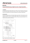
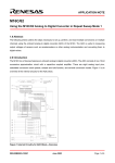
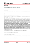
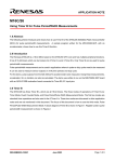
APPLICATION NOTE
M16C/26
Using the A-D Converter In Single Sweep Mode
1.0 Abstract
The following document outlines the steps necessary to setup, perform and read a single sweep conversion
using the onboard analog to digital converter (ADC) of the M16C. The ADC is useful in measuring output
voltages of sensors such as accelerometers or other analog instrumentation and converting them to digital
values.
2.0 Introduction
The Renesas M30262 is a 16-bit MCU based on the M16C/60 series CPU core. The MCU features up to 64K
bytes of Flash ROM, 2K bytes of RAM and 4K bytes of Virtual EEPROM. The peripheral set includes UARTS,
Timers, DMA, and GPIO. The M16C/26 features an onboard analog to digital converter (ADC). The ADC
consists of one 10-bit successive approximation circuit with a capacitive coupled amplifier. There are eight
analog input pins, selectable conversion clock speeds, sample and hold function, and several conversion modes.
Table 1 shows the performance of the ADC and Figure 1 shows a diagram of the ADC block.
Table 1 ADC Performance
Item
Performance
Method of A-D Conversion
Successive approximation (capacitive coupling amplifier)
Analog input voltage
0V to AVcc (Vcc)
Operating clock fAD
fAD, fAD2, fAD3, fAD4, fAD6, or fAD6 or fAD12 where fAD=f(Xin)
Resolution
8-bit or 10-bit (selectable)
Operating modes
One-shot mode, repeat, single sweep mode, repeat mode, repeat sweep mode 0 and
repeat sweep mode 1.
Analog input pins
8 pins AN0 to AN7
A-D conversion start
condition
Software trigger: A-D conversion starts when the A-D conversion start flag changes to “1”
Conversion speed per pin
Without sample and hold function 8-bit resolution: 49 fAD cycles, 10-bit resolution: 59 fAD
cycles. With sample and hold function 8-bit resolution: 28 fAD cycles, 10-bit resolution:33 fAD
cycles.
REU05B0033-0100Z
External trigger (can be retriggered): A-D conversion starts when the A-D conversion start
flag is “1” and the ADTRG/P15 input (shared with INT3) changes from “H” to “L”
June 2003
Page 1 of 8
M16C/26
Using the A-D Converter In Single Sweep Mode
Figure 1 ADC Block Diagram
3.0 Single Sweep Mode Description
In single sweep mode, multiple pins of the ADC can be selected as the input source. Once triggered, a single
conversion takes place on the selected pins and the results are stored in the ADC result registers corresponding
to the selected channels. An interrupt is generated signifying the completion of the conversions. An overview of
the registers that will be used in this example is shown below. These registers are detailed in the included
sample code. For specific details, consult the MCU datasheet. Figure 2 and Figure 3 show the control registers
for the ADC in Single Sweep Mode.
REU05B0033-0100Z
June 2003
Page 2 of 8
M16C/26
Using the A-D Converter In Single Sweep Mode
Figure 2 ADC Control Registers in Single Sweep Mode
REU05B0033-0100Z
June 2003
Page 3 of 8
M16C/26
Using the A-D Converter In Single Sweep Mode
Figure 3 ADC Control Registers
REU05B0033-0100Z
June 2003
Page 4 of 8
M16C/26
Using the A-D Converter In Single Sweep Mode
4.0 Example Program
The following example program demonstrates how to perform a conversion using the ADC with the following
configuration.
• Single sweep conversion
• 10 bit mode
• Analog inputs 0-3 used
• Sample and hold enabled
• Internal Vref
• Conversion clock used will be fAD/4 (When f(Xin) is greater than 10 MHz, fAD must be divided)
• Software conversion start
5.0 Reference
Renesas Technology Corporation Semiconductor Home Page
http://www.renesas.com
E-mail Support
[email protected]
Data Sheets
• M16C/26 datasheets, M30262eds.pdf
User’s Manual
• M16C/20/60 C Language Programming Manual, 6020c.pdf
• M16C/20/60 Software Manual, 6020software.pdf
• Writing interrupt handlers in C for the M16C Application Note
• MSV30262-SKP or MSV-Mini26-SKP Quick start guide
• MSV30262-SKP or MSV-Mini26-SKP Users Manual
• MDECE30262 or MSV-Mini26-SKP Schematic
REU05B0033-0100Z
June 2003
Page 5 of 8
M16C/26
Using the A-D Converter In Single Sweep Mode
6.0 Software Code
The sample software provided was written in C and compiled using the KNC30 compiler. The program performs
one conversion on reset. This code could be modified to use a timer for the trigger of the ADC to provide multiple
conversions at specific intervals. The example program was written to run on the MSV30262 Starter Kit but could
be modified to a user application.
/**********************************************************************
* DESCRIPTION: single_sweep.c
*
*
* PURPOSE: Outlines how to use the M16C/26 ADC in single sweep *
* mode. On reset, program stores the results of the conversions*
* in variables that can be examined using KD30 or similar tool.*
******************************************************************/
#include "sfr26.h"
int TempStore0 = 0x0000; // Location where ADC0 result is stored
int TempStore1 = 0x0000; // Location where ADC1 result is stored
int TempStore2 = 0x0000; // Location where ADC2 result is stored
int TempStore3 = 0x0000; // Location where ADC3 result is stored
#pragma INTERRUPT ADCInt // compiler directive telling where
// the ADC interrupt is located
void ADCInt(void);
/*
** main
* PARAMETERS: None
* DESCRIPTION: Main function. Where program execution starts.
* Sets up the ADC then waits for interrupt to occur.
* RETURNS: Nothing
*/
void main (void){
REU05B0033-0100Z
June 2003
Page 6 of 8
M16C/26
Using the A-D Converter In Single Sweep Mode
adcon0 = 0X10;
/*
00010000; /* AN0, single sweep mode, software trigger, fAD/4
||||||||______Analog input select bit 0
|||||||_______Analog input select bit 1
||||||________Analog input select bit 2
|||||_________A/D operation mode select bit 0
||||__________A/D operation mode select bit 0
|||___________Trigger select bit
||____________A/D conversion start flag
|_____________Frequency select bit 0 */
adcon1 = 0X39;
/*
00111001; /* 10 bit mode, fAD/1, Vref connected, AN0-3
||||||||______A/D sweep pin select bit 0
|||||||_______A/D sweep pin select bit 1
||||||________A/D operation mode select bit 1
|||||_________8/10 bit mode select bit
||||__________Frequency select bit 1
|||___________Vref connect bit
||____________Reserved
|_____________Reserved */
adcon2 = 0X01;
/*
00000001; /* Sample and hold enabled, fAD/4
||||||||______Sample and hold select bit
|||||||_______Reserved
||||||________Reserved
|||||_________Reserved
||||__________Frequency select bit 2
|||___________Reserved
||____________Reserved
|_____________Reserved */
adic = 0X01;
/*
00000001; /* Enable the ADC interrupt
||||||||______interrupt priority select bit 0
|||||||_______interrupt priority select bit 1
||||||________interrupt priority select bit 2
|||||_________interrupt request bit
||||__________reserved
|||___________reserved
||____________reserved
|_____________reserved */
_asm ("
fset i") ;
adst = 1;
while (1){}
// globally enable interrupts
// Start a conversion here
// Program waits here forever
}
REU05B0033-0100Z
June 2003
Page 7 of 8
M16C/26
Using the A-D Converter In Single Sweep Mode
/*
** ADCInt
* PARAMETERS: None
* DESCRIPTION: Interrupt routine of the ADC. Here the converted value is
*
loaded into a variable and masked off to show the result.
* RETURNS: Nothing
*/
void ADCInt(void){
TempStore0= ad0 & 0x03ff;
// Mask off the upper 6 bits of the
// variable leaving only the result
// in the variable itself
TempStore1= ad1 & 0x03ff;
// Mask off the upper 6 bits of the
// variable leaving only the result
// in the variable itself
TempStore2= ad2 & 0x03ff;
// Mask off the upper 6 bits of the
// variable leaving only the result
// in the variable itself
TempStore3= ad3 & 0x03ff;
// Mask off the upper 6 bits of the
// variable leaving only the result
// in the variable itself
}
In order for this program to run properly, ADC interrupt vector needs to point to the interrupt function, ADCInt.
The ADC interrupt vector in “sect30.inc” must be modified as shown below.
;;;;;;;;;;;;;;;;;;;;;;;;;;;;;;;;;;;;;;;;;;;;;;;;;;;;;;;;;;;;;;;;;;;;;;;;;
;
File Name: sect30.inc
;
Content:
Section include file for MSV30262-SKP.
;
Copyright 2003 Renesas Technology America, Inc.
;
All rights reserved
;=========================================================================
;
$Log:$
;=========================================================================
:
:
.lword dummy_int
; DMA1(for user)(vector 12)
.lword dummy_int
; Key input interrupt(for user)(vect 14)
.glb
_ADCInt
.lword _ADCInt
; A-D(for user)(vector 14)
.lword dummy_int
; uart2 transmit(for user)(vector 15)
.lword dummy_int
; uart2 receive(for user)(vector 16)
:
:
REU05B0033-0100Z
June 2003
Page 8 of 8
Keep safety first in your circuit designs!
• Renesas Technology Corporation puts the maximum effort into making semiconductor products
better and more reliable, but there is always the possibility that trouble may occur with them. Trouble
with semiconductors may lead to personal injury, fire or property damage.
Remember to give due consideration to safety when making your circuit designs, with appropriate
measures such as (i) placement of substitutive, auxiliary circuits, (ii) use of nonflammable material or
(iii) prevention against any malfunction or mishap.
Notes regarding these materials
• These materials are intended as a reference to assist our customers in the selection of the Renesas
•
•
•
•
•
•
•
Technology Corporation product best suited to the customer's application; they do not convey any
license under any intellectual property rights, or any other rights, belonging to Renesas Technology
Corporation or a third party.
Renesas Technology Corporation assumes no responsibility for any damage, or infringement of any
third-party's rights, originating in the use of any product data, diagrams, charts, programs, algorithms,
or circuit application examples contained in these materials.
All information contained in these materials, including product data, diagrams, charts, programs and
algorithms represents information on products at the time of publication of these materials, and are
subject to change by Renesas Technology Corporation without notice due to product improvements
or other reasons. It is therefore recommended that customers contact Renesas Technology
Corporation or an authorized Renesas Technology Corporation product distributor for the latest
product information before purchasing a product listed herein.
The information described here may contain technical inaccuracies or typographical errors.
Renesas Technology Corporation assumes no responsibility for any damage, liability, or other loss
rising from these inaccuracies or errors.
Please also pay attention to information published by Renesas Technology Corporation by various
means, including the Renesas Technology Corporation Semiconductor home page
(http://www.renesas.com).
When using any or all of the information contained in these materials, including product data,
diagrams, charts, programs, and algorithms, please be sure to evaluate all information as a total
system before making a final decision on the applicability of the information and products. Renesas
Technology Corporation assumes no responsibility for any damage, liability or other loss resulting
from the information contained herein.
Renesas Technology Corporation semiconductors are not designed or manufactured for use in a
device or system that is used under circumstances in which human life is potentially at stake. Please
contact Renesas Technology Corporation or an authorized Renesas Technology Corporation product
distributor when considering the use of a product contained herein for any specific purposes, such as
apparatus or systems for transportation, vehicular, medical, aerospace, nuclear, or undersea
repeater use.
The prior written approval of Renesas Technology Corporation is necessary to reprint or reproduce in
whole or in part these materials.
If these products or technologies are subject to the Japanese export control restrictions, they must be
exported under a license from the Japanese government and cannot be imported into a country other
than the approved destination.
Any diversion or reexport contrary to the export control laws and regulations of Japan and/or the
country of destination is prohibited.
Please contact Renesas Technology Corporation for further details on these materials or the
products contained therein.