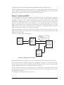
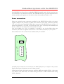
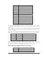
1
HUNT ENGINEERING
Chestnut Court, Burton Row,
Brent Knoll, Somerset, TA9 4BP, UK
Tel: (+44) (0)1278 760188,
Fax: (+44) (0)1278 760199,
Email: [email protected]
http://www.hunteng.co.uk
http://www.hunt-dsp.com
HUNT ENGINEERING
HECPCI9
6U CompactPCI, HEART based
HERON Module Carrier
USER MANUAL
Hardware Rev B
Document Rev D
M. Siggins 30-6-06
COPYRIGHT
This documentation and the product it is supplied with are Copyright HUNT
ENGINEERING 2002. All rights reserved. HUNT ENGINEERING maintains a policy
of continual product development and hence reserves the right to change product
specification without prior warning.
WARRANTIES LIABILITY and INDEMNITIES
HUNT ENGINEERING warrants the hardware to be free from defects in the material and
workmanship for 12 months from the date of purchase. Product returned under the terms
of the warranty must be returned carriage paid to the main offices of HUNT
ENGINEERING situated at BRENT KNOLL Somerset UK, the product will be repaired
or replaced at the discretion of HUNT ENGINEERING.
If HUNT ENGINEERING decides that there is any evidence of
electrical or mechanical abuse to the hardware, then the customer shall have no
recourse to HUNT ENGINEERING or its agents. In such circumstances HUNT
ENGINEERING may at its discretion offer to repair the hardware and charge for
that repair.
Exclusions -
Limitations of Liability - HUNT
ENGINEERING makes no warranty as to the fitness of
the product for any particular purpose. In no event shall HUNT
ENGINEERING’S liability related to the product exceed the purchase fee actually
paid by you for the product. Neither HUNT ENGINEERING nor its suppliers
shall in any event be liable for any indirect, consequential or financial damages
caused by the delivery, use or performance of this product.
Because some states do not allow the exclusion or limitation of incidental or consequential
damages or limitation on how long an implied warranty lasts, the above limitations may not
apply to you.
TECHNICAL SUPPORT
Technical support for HUNT ENGINEERING products should first be obtained from
the comprehensive Support section www.hunteng.co.uk/support/support.htm on the
HUNT ENGINEERING web site. This includes FAQs, latest product, software and
documentation updates etc. Or contact your local supplier - if you are unsure of details
please refer to www.hunteng.co.uk for the list of current re-sellers.
HUNT ENGINEERING technical support can be contacted by emailing
[email protected], calling the direct support telephone number +44 (0)1278 760775,
or by calling the general number +44 (0)1278 760188 and choosing the technical support
option.
2
HUNT ENGINEERING HECPCI9 USER MANUAL
TABLE OF CONTENTS
INTRODUCTION.......................................................................................................... 6
GETTING STARTED ................................................................................................... 8
INSTALLATION ........................................................................................................................................ 8
LEARN HOW TO USE YOUR SYSTEM.......................................................................................................... 9
USING YOUR HECPCI9............................................................................................ 10
HEART ................................................................................................................................................ 12
Nodes ............................................................................................................................................... 12
Features........................................................................................................................................... 12
Stage 1: Configuring HEART .......................................................................................................... 13
Configurations that cannot be achieved .......................................................................................................14
Inter board connection modules...................................................................................................................15
Stage 2: Reading and Writing HEART connections ........................................................................ 15
FPGA modules.............................................................................................................................................16
C6000 modules ............................................................................................................................................16
GDIO modules.............................................................................................................................................17
PCI bus ........................................................................................................................................................17
HERON SERIAL BUS (HSB) ................................................................................................................... 17
HARDWARE RESET ................................................................................................................................ 18
UDP reset ........................................................................................................................................ 18
Software Reset (Code Composer Studio)......................................................................................... 18
PROCESSOR JTAG CONNECTOR ............................................................................................................ 19
CONFIG ................................................................................................................................................. 19
I/OS ....................................................................................................................................................... 20
MULTIPLE BOARD SYSTEMS ............................................................................... 21
IN SAME HOST MACHINE ....................................................................................................................... 21
Installation....................................................................................................................................... 21
Accessing each board ...................................................................................................................... 21
IN SEPARATE HOST MACHINES .............................................................................................................. 21
PROCESSOR JTAG................................................................................................................................. 21
HSB ...................................................................................................................................................... 22
EMBEDDED SYSTEMS WITH THE HECPCI9..................................................... 23
POWER CONNECTIONS ........................................................................................................................... 23
RESET.................................................................................................................................................... 24
C6000 MODULES ................................................................................................................................... 24
MODULES WITH FPGA.......................................................................................................................... 24
GDIO MODULES ................................................................................................................................... 24
HEART CONFIGURATION ..................................................................................................................... 24
JTAG .................................................................................................................................................... 25
MOUNTING THE HECPCI9 .................................................................................................................... 25
HARDWARE DETAILS ............................................................................................. 27
POWER SUPPLIES ................................................................................................................................... 27
BOARD NUMBER SWITCH ...................................................................................................................... 27
MODULE IDS ......................................................................................................................................... 28
HEART ................................................................................................................................................ 28
FIFO CLOCK.................................................................................................................................. 28
Slot ordering.................................................................................................................................... 28
Calculating Latency......................................................................................................................... 29
Multi cast connections ..................................................................................................................... 30
FIFO flushing .................................................................................................................................. 30
Non Blocking connections ............................................................................................................... 30
LEDS.................................................................................................................................................... 30
3
HUNT ENGINEERING HECPCI9 USER MANUAL
DEFAULT ROUTING JUMPERS ................................................................................................................ 31
EMBEDDED POWER CONNECTOR ........................................................................................................... 32
JTAG HEADER ...................................................................................................................................... 32
UNCOMMITTED MODULE INTERCONNECT CONNECTOR ........................................................................ 33
INTER BOARD CONNECTION MODULE .................................................................................................... 34
ACHIEVABLE SYSTEM THROUGHPUT.............................................................. 35
MODULE TO MODULE COMMUNICATIONS ............................................................................................. 35
PCI COMMUNICATIONS ......................................................................................................................... 35
COMMUNICATIONS BETWEEN THE HERON SYSTEM & THE HOST PC. 36
HUNT ENGINEERING API ............................................................................................................... 36
USE of the API................................................................................................................................. 37
DSP SIDE SUPPORT ................................................................................................................................ 37
COMMUNICATIONS BETWEEN HERON MODULES....................................... 39
PHYSICAL DIMENSIONS OF THE BOARD......................................................... 40
FITTING MODULES TO YOUR HECPCI9............................................................ 41
INSTALLING YOUR HECPCI9 HARDWARE ...................................................... 42
SOFTWARE................................................................................................................. 43
DSP PROGRAM ...................................................................................................................................... 43
HOST SIDE PROGRAMS ........................................................................................................................... 43
INSTALLATION OF TOOLS ....................................................................................................................... 44
API IDENTIFIERS FOR THE HECPCI9 .................................................................................................... 45
SERVER/LOADER IDENTIFIERS ............................................................................................................... 45
CODE COMPOSER IDENTIFIERS .............................................................................................................. 45
TROUBLESHOOTING .............................................................................................. 46
HARDWARE ........................................................................................................................................... 46
HOST MACHINE BIOS........................................................................................................................... 46
SOFTWARE ............................................................................................................................................ 46
API................................................................................................................................................... 46
Server/Loader .................................................................................................................................. 47
Code Composer Studio .................................................................................................................... 47
CE MARKING ............................................................................................................. 48
TECHNICAL SUPPORT............................................................................................ 49
APPENDIX A: DETAILS OF THE PCI INTERFACE ........................................... 50
ADDRESS SPACES AND ACCESS MODES ................................................................................................ 50
Configuration Space........................................................................................................................ 50
PCI Vendor ID and Device ID ........................................................................................................ 51
Latency Timer.................................................................................................................................. 51
OPERATION SPACE ................................................................................................................................ 51
Offsets from the Assigned Base Address.......................................................................................... 51
RESET Control ................................................................................................................................ 53
FIFO Access .................................................................................................................................... 54
Empty or Full FIFOs ....................................................................................................................... 54
PCI Burst Transfers......................................................................................................................... 54
PCI Master Mode ............................................................................................................................ 55
Interrupts ......................................................................................................................................... 55
Software Reset Register, offset 0380h ............................................................................................. 55
General Control Register, offset 0340h........................................................................................... 56
General Status Register, offset 0340h ............................................................................................. 56
General Interrupt Register, offset 0341h......................................................................................... 58
Module Information, offset 0380h ................................................................................................... 58
4
HUNT ENGINEERING HECPCI9 USER MANUAL
FIFO Data, offsets 0000h-02FFh.................................................................................................... 60
Inbound FIFO Flags, offset 0300h .................................................................................................. 60
Outbound FIFO Flags, offset 0301h ............................................................................................... 62
FIFOn Write Interrupts, even offsets 0344h-034Eh ........................................................................ 63
FIFOn Read Interrupts, odd offsets 0345h-034Fh.......................................................................... 64
Master Mode Queue Engine, offset 0360h-0377h ........................................................................... 64
Master Mode Interrupt Register, offset 0342h ................................................................................ 65
Master Mode Interrupt Mask Set Register, offset 0342h ................................................................. 66
Master Mode Interrupt Mask Clear Register, offset 0343h............................................................. 67
HSB Data, offset 03A0h................................................................................................................... 68
HSB Control Register, offset 03A1h ................................................................................................ 68
HSB Status Register, offset 03A1h................................................................................................... 69
HSB Slave Address, offset 03A2h .................................................................................................... 69
HSB Master Address, offset 03A3h.................................................................................................. 70
HSB Interrupt Register, offset 03A4h .............................................................................................. 70
HSB Timing Register A, offset 03A5h.............................................................................................. 71
HSB Timing Register B, offset 03A6h.............................................................................................. 71
JTAG Control Register, offset 0381h .............................................................................................. 72
8990 Base Address, offset 03C0h .................................................................................................... 72
JTAG Register, offset 03E0h ........................................................................................................... 73
PCI Data Test Register, offset 0320h .............................................................................................. 73
Special Test Register, offset 03F0h ................................................................................................. 74
Test Information Register, offset 03F0h .......................................................................................... 74
APPENDIX B: DEFINITION OF HEART CONTROL REGISTERS .................. 76
DIRECT SLOT ADDRESSES ..................................................................................................................... 76
SECONDARY ADDRESSES ...................................................................................................................... 76
COMMAND BYTE ................................................................................................................................... 77
FPGA REGISTER ADDRESS ................................................................................................................... 77
Heart-to-Module FPGAs ................................................................................................................. 77
Timeslots Registers......................................................................................................................................78
FIFOx Almost Empty Offset Registers........................................................................................................78
FIFOx UMI Reset Registers ........................................................................................................................78
UMIx Almost-Empty Register....................................................................................................................78
Module-to-Heart FPGAs ................................................................................................................. 79
Timeslots Registers......................................................................................................................................79
FIFOx UMI Reset Registers ........................................................................................................................79
UMIx Almost-Full Register.........................................................................................................................80
HEART “ZAP” ..................................................................................................................................... 80
FPGA REGISTER DATA BYTE ............................................................................................................... 80
EXAMPLE .............................................................................................................................................. 80
5
HUNT ENGINEERING HECPCI9 USER MANUAL
Introduction
The HERON module is a module defined by HUNT ENGINEERING to address the
needs of our customers for real time DSP systems. The HERON module is defined both
mechanically and electrically by a separate HERON module specification that is available
from the HUNT ENGINEERING CD, via the “technology documents” section from the
CD browser, or online from http://www.hunteng.co.uk and going to the user area.
The HERON module specification also defines the features that a HERON module carrier
like the HECPCI9 must provide. HERON stands for Hunt Engineering ResOurce Node,
which tries to make it clear that the module is not for a particular processor, or I/O task,
but is intended to be a module definition that allows “nodes” in a system to be
interconnected and controlled whatever their function. In this respect it is not like the TIM40 specification which was specific to the ‘C4x DSP.
As the HECPCI9 was developed, HUNT ENGINEERING have developed HERON
processor modules that carry various members of the TMS320C6000 family of DSP
processors from TI, and new HERON-IO and HERON-FPGA modules. In addition to
these modules, the HERON specification is a super-set of the pre-existing HUNT
ENGINEERING GDIO module, so the some of the GDIO modules from our C4x
product range can also be used in HERON systems.
The HERON module connects to the carrier board through several standard interfaces.
•
The first is a FIFO input interface, and a FIFO output interface. This is to be used for
the main inter-node communications. (It is used for this on the HECPCI9 and also for
connection to the HOST PC via the PCI bus).
•
The second is an asynchronous interface that allows registers etc to be configured from
a HERON module. This is intended for configuring communication systems, or
perhaps to control some function specific peripherals on the carrier board. (This
interface is not used on the HECPCI9).
•
The third is a JTAG (IEEE 1149.1) interface for running processor debug tools. (This is
implemented on the HECPCI9)
•
The last is the general control such as reset, power etc. (of course these are provided by
the HECPCI9).
HUNT ENGINEERING defined the HERON modules in conjunction with HEART –
the Hunt Engineering Architecture using Ring Technology. This is a common architecture
that we have adopted for our HERON carriers. It provides good real time features such as
low latency and high bandwidth, along with software re-configurability of the
communication system, multicast, multiple board support etc., etc.
However, it is not a requirement of a HERON module carrier that it implements such
features. In fact our customers could develop their own module carrier and add our
HERON modules to it. Conversely our customers could develop application specific
HERON modules themselves and add them to our systems.
The HECPCI9 implements all of the HEART features using dedicated FPGAs that cannot
be considered in the same way as the FPGA on a HERON module. These have their
function fixed by HUNT ENGINEERING at build time. The HECPCI9 is 6U
6
HUNT ENGINEERING HECPCI9 USER MANUAL
CompactPCI card format, interfacing to 33MHz 32bit PCI bus on J1.
The PCI interfaces to a HEART node just like the modules. This means that there are 6
FIFOs in each direction that can be connected to the HEART communications system.
These FIFOs can be accessed as a PCI target interface or a ‘master-mode’ interface allows
the hardware on the HECPCI9 to transfer data between these FIFOs and the host PC’s
memory without the need for the host PC’s processor to copy the data.
The PCI bus also has access to the control functions such as reset, module type, Heron
Serial Bus etc. These are only available as PCI target devices.
Also the PCI bus can access the JTAG test bus controller, allowing debug tools such as
Code Composer to be used without external hardware.
The PCI interface of the HECPCI9 should be accessed using the HUNT ENGINEERING
API software, which provides a consistent interface between software tools and application
programs that run on the host machine and ALL HUNT ENGINERING module carriers.
The HUNT ENGINEERING API has two implementations, a full “development and
target” implementation and a “target only” implementation. The difference is that a
“development and target” API supports the use of development tools, like Code Composer.
This limits these Operating systems to those where Code Composer and the TI Code
Generation tools will run. These are operating systems such as Win 95/98/ME and Win
NT/2000/XP. A “target only” implementation is one where the Module carrier can be
accessed to load and communicate with a pre-developed DSP application. In this case the
HUNT ENGINEERING server/loader tool can also be provided for that operating
system to enable the system to be booted and controlled. These are operating systems such
as Linux, RTOS-32 etc.
For details of operating systems supported at any time please access
http://www.hunteng.co.uk
7
HUNT ENGINEERING HECPCI9 USER MANUAL
Getting Started
The HECPCI9 is a card that plugs into a Peripheral Slot of a CompactPCI host computer.
Any modules that your system has should be fitted to the HECPCI9 and their retaining nuts
fitted, before the HECPCI9 is installed in your host machine (see a later section of this
manual for details).
Normally the default routing jumpers would not be used, and software will be used to
configure the connections between the nodes in your system. If you want to use the default
routing jumpers see the section that discusses them later in this manual.
The PCI bus is by design a "plug 'n play" type bus, so the board is not assigned a base
address by the user, but is assigned this by the host computer’s PCI BIOS or operating
system. After this configuration stage software can interrogate the BIOS or operating
system to establish what the base addresses are.
The HECPCI9, however, provides a switch with which to select the “board number” in the
system. This is the number that the API software uses to access the board. Make a note of
the setting of this switch, and ensure that if you have several HECPCI9s in your system,
that they all have unique switch settings.
In a PC it is necessary that the BIOS has enabled the PCI slot that you are trying to use, and
that bus mastering is enabled and an interrupt is allowed for this slot. Of course all BIOS
setup menus are different, and there will be different options available. The HECPCI9
requires that the slot be enabled so that the base addresses can be assigned, and that bus
mastering and interrupts are enabled to allow the best performance out of any application
code capable of using them.
Installation
The HECPCI9 should be fitted to your cCPI rack (see a later section for advice).
If the machine boots properly then follow the software installation section of the HUNT
ENGINEERING CD.
If you are using Windows 95 or Windows 98/ME the operating system will detect that new
hardware has been installed and will ask you for the device drivers. Choose the option that
lets you continue without installing the drivers, and let the HUNT ENGINEERING
software installation install the drivers.
You can follow the movie provided on how to install your system, found on the HUNT
ENGINEERING CD under the Getting Started section. What this shows you how to do
is:If you have purchased C6000 modules for your system, you will need to install Code
Composer Studio at this point.
Next you should run the install option found under getting started on the HUNT
ENGINEERING CD. First this program will install the HUNT ENGINEERING
Application Programming Interface (API) and run the confidence checks provided with it.
(See the API user manual for details).
Next it will install the HUNT ENGINEERING Software developers pack which is
8
HUNT ENGINEERING HECPCI9 USER MANUAL
required only if you have C6000 modules in your system.
Learn how to use your system
Then, you should follow the movie that explains HEART and how to use it. This is
fundamental to being able to use the HECPCI9. The following section of this manual
explains more about using HEART.
Then there are Getting started examples for C6000s and FPGAs, and tutorials about using
the software tools. You should follow the tutorials that are relevant to your system to learn
how to use it, and get the best use of it.
There are many examples provided on the HUNT ENGINEERING CD, and this is the
best place to start developing your application program.
9
HUNT ENGINEERING HECPCI9 USER MANUAL
Using your HECPCI9
J5 I/O connector.
Used for external
modules
Power connectors for
embedded use (not
normally fitted)
HERON
SLOT 4
HERON
SLOT 2
HERON
SLOT 3
J4 I/O connector.
Used for external
modules
UMI
connector
HERON
SLOT 1
JTAG
header
Power supplies
J1 PCI
connector
Board
number
switch
The HECPCI9 provides four HERON module sockets, each of which can be populated or
left empty. Each module site can accept any 32-bit HERON module, or a subgroup of the
16-bit GDIO modules. The HECPCI9 will automatically configure for the correct module
type without the need for setting any jumpers or software.
The hardware does not impose any limitation on the positions of modules, but the data
paths between modules in a complicated system may only be achievable with a certain
module order. In the first instance fit the modules in whatever order you like.
The connectivity of the HECPCI9 is programmable in software. Once programmed it has
point to point connections between the module sites provided by virtual FIFOs. Each
FIFO is 32-bits wide, but can switch into a 16 bit wide mode if a 16-bit module is detected
by the hardware (see the HERON specification for details of how this is done). Each FIFO
can accept a clock rate of between 60 and 100MHz, allowing a maximum transfer speed
into and out of those FIFOs of 4x100Million bytes/second.
The virtual part of the FIFOS is the ring part of HEART. You do not need to know how
this works, so it is not described here. If you are curious you can read the technology
document from the HUNT ENGINEERING CD, via the “technology documents” section
from the CD browser, or online from http://www.hunteng.co.uk and going to the user
area.
10
HUNT ENGINEERING HECPCI9 USER MANUAL
HEART allows you to connect the output FIFO from one node to the input FIFO of
another, using a time slot that provides a guaranteed bandwidth. Each time slot has a
bandwidth of 66.6 Million bytes/sec. If that is not enough you can allocate more than one
(up to 6) time slots to that connection. Once the virtual FIFO is connected the number of
time slots allocated defines the maximum achievable bandwidth through it.
In reality some other factor will define the bandwidth, perhaps the sample rate of an A/D,
or the speed a processor module can process the data. It is not advisable to allocate more
time slots than are needed, as the resources in a system are finite. This means that if you
allocate excess bandwidth to a connection you might find that your system connectivity is
impossible to achieve.
Once the virtual FIFO is connected, C6000 processor modules will access them using
HERON-API, FPGA based modules will access them using the FIFO access components
(VHDL) provided by HUNT ENGINEERING.
11
HUNT ENGINEERING HECPCI9 USER MANUAL
HEART
The Hunt Engineering Architecture using Ring Technology (HEART) is a novel
communications system that forms the inter-node connections of the HECPCI9. It allows
the connections on your HECPCI9 to be configured in software rather than the
conventional use of cables that are messy, unreliable and low performance. Details of that
architecture can be read elsewhere, as a user does not need to know them. Here we must
describe the features it provides and how to use them.
Nodes
Your system is made up of nodes. We use that term because it does not differentiate
between processor modules, FPGA modules, I/O modules, connections between boards or
even Host computer connections (PCI bus interface in the case of the HECPCI9). HEART
treats all of these “nodes” as equal. The HEART architecture considers each “board” to
have 6 nodes, and there can be as many boards as you need in your system.
Features
HERON modules are designed to be interfaced to carrier boards that provide synchronous
FIFOs.
HEART provides these FIFOs in a way that allows the FIFOs to be connected using
software. We talk about these connections as virtual FIFOs, but they are in fact two FIFOs,
each with one end connected to a HERON module socket and the other end connected to
HEART which transports data between them.
HEART is used in two phases. The first phase is to make the connections in your system.
This is equivalent to placing a phone call – not a real time operation, more of a system
configuration phase.
Once the connection is made, the virtual FIFO operates exactly like a hardware FIFO,
where each module uses the status flags provided at the module socket to determine if and
when data can be transferred. The HEART part of that connection is transparent, and the
12
HUNT ENGINEERING HECPCI9 USER MANUAL
connection operates in real time (guaranteed bandwidth and calculable latency).
There are additional features that are useful in a real time Digital Signal Processing system
such as Multi-cast data paths, FIFO flush, programmable FIFO flags etc. These are for the
advanced user, and are discussed more fully later in this manual.
Stage 1: Configuring HEART
To use HEART you first need to decide the connections that you need between the nodes
in your system. It is an idea to draw your system as a block diagram, where each block
represents a node in your system. Now draw connections between your nodes. Each
connection should represent a data or control path. There can be more than one connection
between the same nodes if the system needs it, e.g. one for data flow and one for control
data. Actually there can be connections that send the same data from one place to many
(multi-cast). If your system needs more than 4 modules, or physically separate sub-units
then you’ll have more than one board in your drawing.
You must label the connections with FIFO numbers at each end. You cannot re-use the
same FIFO number more than once in each direction for each node. Then choose slot
numbers for each node.
So you may end up with a drawing like :-
Node A
(Slot1)
Needs
100Mbytes/sec
Node B
0
0
2
(Slot2)
1
0
1
3
4 (Slot3)
Node D
0
0
(Host)
0
Node C
Example of Requirements sketch.
Remember that the host PCI interface is also a node, and should be drawn in this sketch.
Notice that the choice of FIFO number is not important as long as it is not used more than
once. Notice also that the FIFO number of each end does not have to be the same, and that
a high bandwidth connection is still allocated only one FIFO.
Now you need to enter your connections into the “network file”. Full details of this can be
found in the Server/Loader user manual. The same file format is used by the Server/Loader
and the heartconf utility.
An example of a file that defines the above is:-
13
HUNT ENGINEERING HECPCI9 USER MANUAL
# For HUNT ENGINEERING's Device Driver API use:
# BD API
Board_type
Board_Id
Device_Id
#---------------------------------------------------------------------# Using API
BD API HEP9A 0 0
#
# Nodes description
# ND BD_nb ND_NAME ND_Type CC-id HERON-ID filename(s)
#------------------------------------------------------------------c6
0
NodeA
ROOT
(0)
00000001 mydspprog.out
fpga 0
NodeB
normal
00000002
fpga 0
NodeD
normal
00000003
ibc 0
pcif 0
ibc1
NodeC
normal
normal
0x06
0x05
#-----------------------------------------------# Number of the link connected to the host system
# HOSTLINK PORT
#-----------------------------------------------TOHOST
0
FROMHOST 0
#-------------------------------------------------------------------#
from:slot fifo to:slot
fifo
timeslots
#-------------------------------------------------------------------heart
heart
heart
heart
NodeA
NodeA
NodeC
NodeD
0
1
0
3
NodeB
NodeB
NodeD
NodeB
0
1
0
2
1
1
1
2
BDCAST MyData NodeB 0 1
LISTEN MyData NodeC 0
LISTEN MyData NodeD 4
Notice the multi-cast connection is set using BDCAST and LISTEN entries, and that the
connection between Node D and Node B allocates 2 timeslots to give enough bandwidth
for the 100Mbyte/sec connection.
The HeartConf or the Server/Loader program will translate this file into a set of
connections.
If there is no error message then you don’t need to do any more.
Configurations that cannot be achieved
If you receive an error message when you run HeartConf or the Server/Loader, of which
there are many kinds, you need to read the message carefully to see what might be the
cause.
If your message is of the type “Cannot place HEART statement……” or “Cannot place
BDCAST statement…” then it may be because you have tried to use more resources than
are available at a particular point in your system.
In that case you need to look at the way you have placed your nodes in the system.
Taking our diagram of HEART, and adding the slot numbers in the order that they are
connected on the HECPCI9, we can draw the connections in our example system above:-
14
HUNT ENGINEERING HECPCI9 USER MANUAL
In our case the segments that are most heavily loaded have only 4 timeslots used, so there is
no problem, but you can see that moving the module from Slot 1 into Slot 4 would mean
only one segment has 4 timeslots loaded. This could free up some resources for other parts
of your system, which might be critical if your system was more complicated.
Inter board connection modules
When you have more than one board in your system, you simply draw the connections
between them as connections through the inter board I/O node.
The specification of the inter board module will govern how many connections are possible
and what bandwidth they support. It is normally advisable to minimise the connections
between boards in the same way that we have just shown it is better to move NodeA into
slot 4 above. You may find it better to move certain modules from one board to another to
reduce the number of connections required.
Stage 2: Reading and Writing HEART connections
Once you have configured your HEART connections, they can be treated as FIFOs. These
FIFOs are point to point in one direction at a time. There are flags available to determine if
there is room to write data into one end, and different flags available to determine if data
can be read from the other end.
Multi-cast connections are the same, just that the HEART communications system puts a
copy of the data into each receiving FIFO.
By default the FIFOs operate in blocking mode. That is, if the receiver stops reading, the
FIFO will eventually become full. Then the sender will not be able to write any more as the
FIFO flags will indicate that there is no space.
There are some advanced options discussed later in this manual, but most users should use
15
HUNT ENGINEERING HECPCI9 USER MANUAL
the connections made in Stage1 like this – each one is essentially a single point to point
FIFO.
FPGA modules
A HERON module that has a user configurable FPGA, has the pins of the HERON
module connected to the pins of the FPGA. So the “program” for the user FPGA needs to
correctly interpret the FIFO signals to access the FIFOs.
Normally this will be done using the Hardware Interface Layer that HUNT
ENGINEERING provides for these modules.
The FPGA has a separate 32 bit data path for Input and Output FIFOs, so can read one
FIFO and Write one FIFO at the same time. If the “Almost” flag shows that there are
many things that can be done, i.e. an Input FIFO is not Almost Empty, or an Output FIFO
is not Almost Full, the FPGA can transfer data at the rate of one 32bit word per FIFO
clock. The FIFO clock of the HECPCI9 must be between 60 and 100MHz, so the transfer
can take place at between 240 and 400 Million bytes per second. Normally the HEART
connection will not be configured for this much bandwidth, so eventually the Almost flag
will be asserted. Then the transfers must check the “limit” flag before each transfer. The
data is then transferred more slowly than one data item per clock depending on the logic
used.
The Hardware Interface Layer provided for the FPGA by HUNT ENGINEERING takes
care of these things automatically, while presenting to the user a simple friendly interface.
C6000 modules
A HERON module with a C6000 processor will have registers where the flags of the FIFOs
can be read, and separate addresses in its memory map where each FIFO can be
read/written. The hardware will have features that allow the DMA engines of the processor
to access these FIFOs. The users program for the processor must include the software that
accesses the FIFOs using DMAs or direct processor access. The software needed will be
different depending on the Module hardware design.
Normally the HERON-API software will be used to access these FIFOs, linked into the
user program for the DSP.
C6000 processors usually have only one memory bus connected to the FIFOs, so it is not
possible to read a FIFO and write a FIFO at the same time. That is any bus cycle can be
either a read or a write but not both. Transfers can occur in both directions at once, by
alternating the direction of the cycles, but this means the 240 to 400Million Bytes/second of
the HERON interface is shared between reads and writes.
Usually to get the most efficient access of the FIFOs, the processor will use the “Block”
flags to indicate that it is possible to transfer a block of data. On the HECPCI9 the Block
flags indicate that it is possible to transfer 64 words (32 bits wide). With the right hardware
on the module it is possible to DMA data on consecutive FIFO clocks during this burst,
but at the end of a burst the processor will need to take some actions to enable the next
burst. When the transfer size is below the block size, the processor must transfer the data
one word at a time, testing the limit flag between each transfer. This means it will take at
least one cycle to read the flags, and another to access the FIFO data. In reality the C6000
architecture does not allow these processor driven accesses to be achieved in a single cycle
and each one may take a few tens of cycles. This makes the transfer of small blocks of data
16
HUNT ENGINEERING HECPCI9 USER MANUAL
quite inefficient. To help alleviate this problem the HECPCI9 provides “Almost” flags that
are programmable. Then if a connection will always be used to transfer a small block that
has a constant size, the Almost flag can be set to indicate that a transfer of that size can take
place. Then the processor only has to test one flag in order to transfer the whole block.
Functions in HERON-API handle these issues for you, allowing you to use read and write
calls to start transfers and then offering you a choice of ways that you can be informed
when the transfer has completed. HERON-API offers you a consistent interface regardless
of the hardware design of the particular module you are using.
GDIO modules
GDIO modules have a subset of the HERON module pins only. They are 16 bit modules
with no user programmability. They can only access FIFO #0 of the module slot, and this
access is made by the hardware of the module.
Typically GDIO module transfers cannot be blocked, and data will be lost if the FIFO
reaches its limit (full or empty), but this is not always the case.
The HECPCI9 automatically detects that the module is a 16 bit version, and packs two of
these 16 bit entities into each 32 bit word. The first 16 bit item is the lowest 16 bits of the
32 bit word. This is only implemented on FIFO #0 as this is the only one connected to a
GDIO interface.
The “other” end of the FIFO connection will be accessed as the normal 32 bit interface.
PCI bus
The PCI bus has access to the Host node of HEART. This means that the six input and six
output FIFOs can be accessed by the Host PC using the PCI bus. The PCI bus has only
one data path, so it is possible to perform a read or a write but not both in the same cycle.
Transfers can occur in both directions at once, by alternating the direction of the cycles, but
this means the 133 Million Bytes/second of the PCI bus is shared between reads and writes
The Host PC can use various flags to determine how many 32 bit words can be transferred
at a time. It can also use the PCI Master Mode hardware of the HECPCI9 to program
hardware controlled transfers in a “DMA like” way.
The HUNT ENGINEERING Host API is usually used to access the PCI devices, as it
provides the most efficient use of the PCI hardware from any of the supported Host PC
operating systems. In all of these Operating Systems the software interface provided to the
users program and the development tools is the same. It is even consistent between
different HERON Module carriers.
Heron Serial Bus (HSB)
The HECPCI9 provides a Heron Serial Bus that runs between the Nodes. This provides a
non-real time interface for configuration type messages.
On the HECPCI9 HSB is also connected to the FPGAs that implement HEART, and it is
this interface that is used to configure your HEART connections. Normally HEART is
configured using HeartConf or the Server/Loader tools on your Host PC. These tools
access HSB using the HOST-API software to ensure that there are no resource conflicts.
It is also possible however to configure the HEART connections from a C6000 or FPGA
17
HUNT ENGINEERING HECPCI9 USER MANUAL
module. This is useful when the HECPCI9 is being used as an embedded Module Carrier,
but it can also be used by “advanced” users to reconfigure your system during operation.
Great care must be taken when doing this so it should not be attempted unless you
understand the consequences of what you are doing.
A C6000 module would access the HSB using functions provided in the HERON-API, and
an FPGA module would access HSB using the HE_USER interface in the Hardware
Interface layer provided.
HSB can be used for other system configuration or control messages, i.e. it is used by the
hrn_fpga utility to download the user configuration from the PC to an FPGA module.
It must be remembered though that the HSB is not only slow, it is also arbitrated, so it
cannot be relied upon for real time operation unless your system is carefully defined so that
arbitration failures will never occur.
Hardware Reset
Before the HECPCI9 can be used, it must receive a Hardware reset. Actually, the
HECPCI9 generates such a reset on power up. This is generated using a CR delay so that
the reset remains asserted for some time after the power supplies are stable. This is useful
for when the HECPCI9 is being used “stand alone” in an embedded system.
The reset can be re-asserted via the PCI bus reset, or a register in the address space of the
PCI interface.
The HOST-API function HE_RESET allows control of this register based function.
This reset initialises all of the HECPCI9 circuitry and the modules on it into a known state.
This includes disconnecting and emptying the FIFO connections between the modules.
It applies the Module Reset signal to all of the modules fitted to the HECPCI9, including
inter board modules that might propagate that reset to other boards in your system.
Module Reset however does not “clear” the contents of an FPGA based module.
When the reset is asserted the LED on the back of the HECPCI9 labelled “RESET” will
light up. When the reset is removed it will no longer be lit.
When running a tool like the HUNT ENGINEERING server/loader, the reset LED will
flash for a short time when the system is reset prior to booting.
UDP reset
Each HERON module has a UDP reset pin that it can assert. It is not usual for a processor
module to assert this, but a communications module like the HEGD7 can drive this signal.
This is used to reset the board in preparation for remote booting via that communications
module. The UDP reset line from each HERON module slot is simply ORed with the PCI
reset to generate the hardware reset signal.
Software Reset (Code Composer Studio)
Code Composer Studio has a menu that allows “DSP reset”. This must never be confused
with the hardware reset controlled via the PCI bus – it is not the same thing. The Code
Composer “DSP reset” simply resets some of the internal registers of the DSP but will
NOT empty HEART FIFOs. It will also only affect the DSP where the menu is selected,
18
HUNT ENGINEERING HECPCI9 USER MANUAL
and cannot affect any I/O boards in the system.
The reset LED will not flash when a DSP reset is made from Code Composer Studio.
HUNT ENGINEERING provides a Reset Plug-in for Code Composer Studio that allows
you to use the Hardware Reset from within Code Composer. This does affect all of the
modules, and clear the HEART FIFOs.
Processor JTAG connector
The Processor JTAG connector is provided to allow access to the JTAG connections of the
HERON modules, from an external emulator, in order to run Code Composer Studio, (the
development environment for the ‘C6000 processors). These connections are not used by
FPGA modules, but are connected to a C6000 processor on a C6000 HERON module.
The design of the HERON module means that the HECPCI9 can determine if a HERON
slot does not contain a module, or contains a module that does not implement JTAG.
The HECPCI9 hardware will therefore be automatically configured correctly for the
HERON modules fitted.
Code Composer Studio needs to be configured to understand how many processors there
are in the chain. When this is done please note that the hardware JTAG chain is connected
to slot 1, then slot 2 then slot 3 and finally slot 4. Different versions of Code Composer
Studio list these in different orders during setup so be careful when setting CCS up
manually.
The connector is a standard 14 way JTAG connector as used by TI on their emulators such
as the XDS510, XDS560, and also by compatible emulators from other companies. This
includes the HEPC9 from HUNT ENGINEERING.
The connector on the HECPCI9 is a simple 0.1 inch header in a 7x2 configuration. It
accepts the standard connector on most emulators, but beware that the C6000 JTAG chain
is a 3.3V one. For this reason 5V JTAG emulators should not be used.
The JTAG header on the HECPCI9 can also be used to connect multiple boards together
in the same JTAG chain. See the later sections in this manual for details on using this
header.
Config
There is a system wide Config signal that is open collector and hence requires a pull up to
be provided by the carrier board. The HECPCI9 provides this pull up. Each processorbased module will drive this signal low after a Hardware reset. It can then be released under
software control after booting.
The Config signal is provided for any hardware that needs to be disabled until the entire
system has booted. If there is any hardware that uses this feature it will not function until all
processors have removed their config signal.
The Config is buffered and used to control an LED labelled "CONFIG" on the back of the
HECPCI9. This LED will illuminate when the config signal is asserted (low).
19
HUNT ENGINEERING HECPCI9 USER MANUAL
I/Os
There are some “Uncommitted Module Interconnect” (UMI) signals defined by the
HERON specification, which are simply connected to all modules.
These are intended to connect control signals between modules, for example a processor
module can (via software) drive one of these signals with one of is timer outputs. Then if an
I/O or FPGA module is configured to accept its clock input from one of these signals, it is
possible to implement a system with a programmable clock. There will be other uses for
these signals that are module design dependent.
The HECPCI9 pulls these signals high with 10K resistors.
The HECPCI9 also connects these four signals to the UMI connector near the rear edge of
the board.
20
HUNT ENGINEERING HECPCI9 USER MANUAL
Multiple board systems
You can fit multiple HECPCI9s into your system. They can be in the same Host PC, or in
separate machines or racks. Usually these multiple boards will be connected using an Inter
board module. The specification of that module will define what is and is not possible, but
as a minimum it will be possible to route HEART connections to and from that Inter board
module, which will be connected by that module to the other Module carrier in your system.
In same Host machine
In the case where you are installing more than one HECPCI9 in the same Host PC, all you
need to remember is to set the red board switch to a different setting on each board.
Installation
The HOST-API will access multiple boards in your system. The recommended way to
install multiple boards is to begin by installing a single board only. When that installation
has completed and all the confidence checks have passed, then you can shut down your PC
and fit the other boards. When the system is powered up the new boards should be detected
and the drivers installed. It is then advisable to use the Confidence checks from the
ProgramsÆHUNT ENGINEERING Æ group to check each board individually.
Accessing each board
When installation is completed, the PCI bus will have allocated separate resources to each
board. These boards can be accessed using HOST-API.
To specify which board to access the “Board number” variable in the open calls to HOSTAPI need to be set to the same setting that you selected on the Board switch of that board.
In separate Host machines
When the boards of your system are in separate host PCs, it is still a good idea to choose
different board numbers, in case the inter board modules you have connect the HSB. HSB
uses a combination of the Board number and the slot number to form its addresses.
Processor JTAG
The HECPCI9 JTAG header allows you to connect multiple boards together in the same
JTAG chain. It is not always necessary to do this as Code Composer can be run separately
on each board, but if you want to run a single Code Composer session across multiple
boards you need to connect the JTAG chain as one single chain.
The JTAG header on the HECPCI9 can be used as an input or an output – selected via the
PCI bus. On reset the HECPCI9 configures the JTAG chain to be a slave of the JTAG
header, i.e. the header is an input, and it is used to drive the JTAG paths of the HECPCI9.
When the HOST-API resets the HECPCI9 the board is set to use the on board circuitry to
control the JTAG chain. This is the “normal” mode of operation.
21
HUNT ENGINEERING HECPCI9 USER MANUAL
In the multiple board situation you need to set the first board as a Master board, and have
the following boards as slaves. For details of how to do that see the Windows HOST-API
user manual.
Note that the “default” after reset is to be a slave of the JTAG header – the setting required
by all except the first board in your system. This allows the multiple board JTAG to be
supported even if the host PC does not have access to the JTAG switch on those boards.
An example of this is using a Master board in a PC to debug an embedded board that has
no connection to a PCI bus.
HSB
The HSB can be connected between multiple boards in a system, but that would be a
capability of the Inter board module. Refer to the user documentation of your particular
Inter board module for details.
22
HUNT ENGINEERING HECPCI9 USER MANUAL
Embedded systems with the HECPCI9
The HECPCI9 can be used as an embedded HERON module carrier. In this case there are
no connections to the PCI bus necessary. The HEART will run to provide communications
and the modules will operate just the same as when the assembly is fitted to a PC.
Power connections
There are optional power connectors provided on the HECPCI9 that allow the power
supplies needed to be powered via cables and connectors. The main connector provides
+5V and +12V using a standard PC Disk drive connector. The HECPCI9 uses only the +5
power and generates +3.3V and +2.5V from this. The +12V is used by some modules but
not all – check the user manuals for each module for details.
Very few modules use –12V, so normally it is enough to use just the Disk drive type
connector, but there is a separate connector for –12V is that is necessary in your system.
The connections to the connectors are marked clearly on the PCB:-
GND
-12V
+12V
+5V
GND
GND
Normally these connectors are not fitted to the HECPCI9, but if you request it they can be
fitted at the factory, otherwise you can fit them yourself.
If fitted at the factory, the larger connector would be AMP part number 350211-1 (the same
as is fitted to a PC disk drive). A suitable mating connector is AMP 1-480424 with crimp
AMP 1-480426-0.
23
HUNT ENGINEERING HECPCI9 USER MANUAL
The smaller connector would be fitted with a latching KK type connector Molex part
number 22-04-1021. A suitable mating connector is Molex 22-01-1023 with crimp type 0850-0032.
Reset
The HECPCI9 automatically generates a reset signal following power up. This means that
the system will be properly initialised if you simply “switch on” the power.
If you feel the need for an external reset signal, there is a small 2-pin jumper above the J1
connector on the HECPCI9. It is misleadingly labelled JTAG, but is in fact a reset input.
The connector its pin 2 connected to ground. The other pin, pin 1, (identified with the silkscreen square around it), is an input to the PCI FPGA on the HECPCI9, pulled to 3.3V
with a 10K resistor. When the two pins are connected together the HECPCI9 will be reset,
but the same can be achieved by driving a logic signal onto this connector. A low level is
taken as a reset.
There is a certain amount of de-glitching applied to this signal to allow the direct
connection of a switch that might exhibit some contact bounce. Any low level of less than
100nS will be ignored. After the low level is detected the reset will be held low for
approximately 0.2S. Any low pulses during that time will re-start the timing of the 0.2S.
C6000 modules
A C6000 HERON module boots the processor from some on board FLASH ROM.
Normally this is a pre-boot that initialises the hardware and starts to accept a boot stream
from a FIFO.
In an embedded system there is no way to boot your application program onto the module
using the FIFOs. In this case you must program your application into the on board FLASH
ROM. Utilities and instructions that help you do this can be found on the HUNT
ENGINEERING CD.
Modules with FPGA
Modules that have FPGAs can have PROMS fitted to them that initialise the FPGA with
your application program. You need to refer to the user manual of the particular module
that you are using for details of the options provided and how to use them.
GDIO modules
GDIO modules do not require any programming but are simply hardware that starts to run
after reset.
HEART configuration
Even in an embedded system the HEART connections need to be initialised. Simple
systems might be able to use the Default Routing Jumpers discussed in a later section of this
manual.
24
HUNT ENGINEERING HECPCI9 USER MANUAL
Most systems however will need to “nominate” a module in the system to perform this
initialisation.
A C6000 module can use the HERON-API functions to access the HSB, and hence have
the HEART initialisation embedded in the application software.
A module with an FPGA can use the HE_USER interface in the Hardware Interface Layer
to initiate HSB messages. In this way the HEART configuration can be stored in a ROM
component in the FPGA.
JTAG
The HECPCI9 defaults to using the JTAG header as an input that will master the JTAG
chain. Hence an embedded HECPCI9 can accept a JTAG input from another HECPCI9 or
a TI XDS510 or XDS560 without requiring any further set up.
Mounting the HECPCI9
The HECPCI9 is supplied with hardware for fitting it into a CompactPCI host machine.
This can be removed when the board is to be embedded. Two screws hold front panel.
When these have been removed, the fixing holes can be used to mount the HECPCI9 in
your system. Because of the height of the HECPCI9 it is also recommended that one or
more fixings are used in the centre of the board. The Module Fixing positions can be used
for this purpose.
T
U
V
W
X
M
L
K
J
I
H
E
G
F
D
C
B
A
N
O
P
25
Q
R
S
HUNT ENGINEERING HECPCI9 USER MANUAL
Reference
Description
Dimension
A
Bottom edge to lower panel fixing
5.5 mm
B
Bottom edge to Slots 1 and 2 top outer fixing
37.5 mm
C
Bottom edge to Slots 1 and 2 top inner fixing
42.5 mm
D
Bottom edge to lower centre panel fixing
94.5 mm
E
Bottom edge to Slots 1 and 2 bottom inner fixing
115 mm
F
Bottom edge to Slots 1 and 2 bottom outer fixing
120 mm
G
Bottom edge to Slots 3 and 4 bottom outer fixing
132.77 mm
H
Bottom edge to Slots 3 and 4 bottom inner fixing
137.77 mm
I
Bottom edge to upper centre panel fixing
138.85 mm
J
Bottom edge to Slots 3 and 4 top inner fixing
210.27 mm
K
Bottom edge to Slots 3 and 4 top outer fixing
215.27 mm
L
Bottom edge to upper panel fixing
227.85 mm
M
Board height
233.35 mm
N
Left edge to panel fixings
3.57 mm
O
Left edge to Slot 2 right side fixings
18.726 mm
P
Left edge to Slot 2 left side fixings
72.726 mm
Q
Left edge to Slot 1 right side fixings
84.776 mm
R
Left edge to Slot 1 left side fixings
138.776 mm
S
Left edge to rear optional mounting holes
140.07 mm
T
Left edge to Slot 4 left side fixings
17.226 mm
U
Left edge to Slot 4 left side fixings
73.226 mm
V
Left edge to Slot 3 right side fixings
85.266 mm
W
Left edge to Slot 3 right side fixings
139.266 mm
X
Board length
160 mm
26
HUNT ENGINEERING HECPCI9 USER MANUAL
Hardware Details
The following sub-sections provide details on the hardware such as connector pinouts and
signal levels etc, but they are placed here, as the "system" configurer does not normally need
this information. It is, however, necessary for a user who needs to develop compatible
hardware or for use in system troubleshooting.
Power supplies
The HECPCI9 is a 6U CompactPCI peripheral board. It is a 5V only card as defined by the
CompactPCI specification – it makes no connection to the backplane 3.3V supply.
Connection IS made to the +12V and –12V supplies, for possible use by modules, although
the HECPCI9 does not use these supplies itself.
Voltage
Typical (& measured)
Maximum
+5V
2.7A
4.0A
+12V
0
0
-12V
0
0
Remember when calculating system power that the power requirements of each module
must be added to these.
Board Number Switch
The only user configurable option on the HECPCI9 is the board number switch. This
switch can be turned by hand and a hexadecimal number between 0 and F is displayed to
indicate its current setting.
The number selected by this switch is the “board number” that must be used when
accessing this board using the HUNT ENGINEERING API software. This is achieved by
the driver layer of the API reading the switch value, and using this to identify this card to
the upper layers of the API.
The value of this switch is also used by the HERON processing modules when they are
booted. This is to make sure that they do not boot from data intended for another
processor. Refer to the user manual of the relevant HERON processing module for details.
The HSB also uses the board number setting to address the nodes.
There is no restriction on the setting of this switch other than there cannot be two boards
on the same PCI bus with the same setting of this switch.
27
HUNT ENGINEERING HECPCI9 USER MANUAL
Module IDs
Each node of the HECPCI9 has a slot number assigned to it, as defined in the HERON
specification. The combination with the Board number switch and this slot ID allows the
module to identify itself uniquely in the system.
The boot prom of the HERON processing modules use this for boot purposes as does the
HSB for addressing particular nodes.
Node
Slot ID assigned
HERON slot 1
1
HERON slot 2
2
HERON slot 3
3
HERON slot 4
4
Host node
5
Inter board module
6
HEART devices
7
HEART
How to use HEART is described in the earlier sections of this manual.
How HEART works is described for the interested reader in a separate technical document
that can be found on the HUNT ENGINEERING CD. Please note that it is not necessary
to understand how HEART works – this is just background information.
FIFO CLOCK
The FIFO clocks on the HECPCI9 are according to the 100MHz FIFO timings shown in
the HERON module specification. The clock has a minimum frequency of 60MHz and a
maximum frequency of 100MHz.
The clocks from each module, and the read and write clocks can all have different
frequencies with any phase relationship.
Slot ordering
To make the signal routing on the HECPCI9 simpler and reliable the HEART devices are
connected in an order that is perhaps not what you expected. The HEART is connected as
:ÆHost node Æ Slot1 Æ Slot3 Æ Inter board node Æ Slot 4 Æ Slot2 Æ Host node
This should not affect how you use HEART, but is sometimes important to understand if
your system configuration uses a lot of resources.
It is also important to understand this ordering if you need to calculate the Latency between
nodes.
28
HUNT ENGINEERING HECPCI9 USER MANUAL
Calculating Latency
One feature of HEART is that the latency of a communication is controlled within limits
that can be calculated. The way that the connections of HEART are pre-connected means
that there are no arbitration delays. It is also not possible that a connection will fail to
connect – it is already connected before the data is sent.
The use of FIFOs means that the latency varies depending on how you use them. For
example if you use a block flag to determine when to write, that write may be delayed until
there is space.
If we consider the simple case of using the limit (full and empty) flags, and a connection
that has no data in either FIFO, we can calculate the limits of the latency as follows:1. Writing a data item to the FIFO will take two FIFO clocks.
2. That data will be available to the HEART system after 13 cycles of 100MHz
3. The time slots travel around the HEART ring constantly, so the longest wait for a
slot will be five 100MHz clocks, the data will be placed onto the ring in the sixth
clock at the latest.
4. The data is clocked around the ring constantly, and takes 4 clocks to pass through
each node that is not receiving the data. For the sending node it takes one clock to
be passed on, and on the receiving node it takes one clock to be received.
5. The data is written into the FIFO on the next 100MHz clock.
6. That data will flow through the FIFO, in 6 cycles of 100MHz,
7. The Empty flag will be set after 3 cycles of the FIFO clock.
8. The data item can be read on the next FIFO clock.
i.e. items 1, 7 and 8 make a total of 6 clock cycles at the FIFO clock. Items 2,3,4,5 and 6
make a total of 20+(4*number of nodes passed)+(up to 5) clock cycles at 100MHz.
Any inter-board connections will add to this latency, the exact amount will be dependent on
the module design. Refer to the user documentation of the module for a precise definition.
The calculations above show that there is a very small amount of uncertainty, and even if we
take the maximum spread that we can achieve with a single board we see :Adjacent slots using maximum FIFO clocks (minimum latency): 260ns to 310ns
From slot to itself using minimum FIFO clock frequency (maximum latency) 500ns to
550ns.
29
HUNT ENGINEERING HECPCI9 USER MANUAL
Multi cast connections
It is possible to use “special” connections with HEART, where more than one receiver can
receive the data sent by one node. This is achieved because the receiver of a time slot does
not destroy the data, it continues around the HEART.
As you can see from the earlier sections of this manual this is achieved by specifying the
sender and each receiver separately in the network file for your system.
FIFO flushing
A special feature of the HEART is that the FIFOs in a connection can be cleared by a
module asserting one of its UMI lines. In that case the clearing event is programmed for a
FIFO using the HSB configuration registers. Multiple FIFOs can be programmed to
“flush” on the same UMI line, so sending and receiving halves of the same connection can
be cleared, or even, multiple connections cleared without asserting the hardware reset.
Normally this feature will be selected by the HEART configuration tool. Once this setting is
selected for a particular FIFO, the flushing can take place by writing the UMI as an output
from a C6000 module or simply driving the UMI line from an FPGA.
For definitions of those registers see the appendix of this manual.
Non Blocking connections
Another feature of HEART is to allow receivers to “listen” to a connection but not block
that connection if the FIFO becomes full. This can be useful if the sender has no way of
stopping the transmission, or if the node is simply monitoring data and it does not matter if
data is lost. Often this will be used in conjunction with the FLUSH feature.
This selection is also made via the HSB control registers in the HEART device, and is also
normally selected by the HEART configuration tool.
For definitions of those the HSB registers see the appendix of this manual.
LEDS
There are many LEDS on the reverse side of the HECPCI9, most of them are used to
indicate if the FPGAs that form the HEART are properly configured from their PROMS.
Next to each FPGA that should flash briefly on power up, but then remain off. This shows
that the FPGA has configured. If at any time one of these LEDs is illuminated, try
powering your system off (that is switch off, not re-boot) and back on again. If the LED is
still illuminated then there is a hardware fault and you should contact Technical support at
your supplier.
At the front edge of the board, on the reverse side, there are five more LEDS:
Two of these LEDS are labelled 2.5V and 3.3V. These are normally illuminated to indicate
that their respective power supply circuits are functioning. If either of these is not
illuminated then the Power supply is not working. This could be because you short-circuited
a connection and the safety feature has activated to prevent damage to your hardware. If at
any time one of these LEDs is not illuminated, try powering your system off (that is switch
30
HUNT ENGINEERING HECPCI9 USER MANUAL
off, not re-boot) and back on again. If the LED is still not illuminated then there is a
hardware fault and you should contact Technical support at your supplier.
There is another LED labelled “SYNC LOSS”. This is illuminated if the HEART ring is
receiving corrupted control data. This normally indicates that there is a failure of the
hardware. If at any time one of these LEDs is illuminated, try powering your system off
(that is switch off not re-boot) and back on again. If the LED is still illuminated then there
is a hardware fault and you should contact Technical support at your supplier.
The remaining two LEDs are indicators of the state of the Reset and Config lines. They are
labelled “RESET” and “CONFIG” and illuminate when the respective signal is asserted
(low).
Default Routing Jumpers
The default routing jumpers are provided by HERON modules and GDIO modules as built
for use in HERON systems. These are the longer pins on the topmost HERON connector
of the module. These pins protrude above the HERON/GDIO module when it is fitted to
the HECPCI9 to which jumper links can be fitted.
|Å output
Æ|Å input
5
0 5 4 3 2 1 0
4 3 2 1
Æ|
On the HECPCI9 these jumpers are used to select which the connections of timeslots to
FIFO #0 following a hardware reset.
For example with the jumpers as fitted in the diagram, Input FIFO#0 will be receive data
from time slot 1, and Output FIFO#0 will write data to time slot 1.
If more than one jumper is fitted at the same time then all of those time slots will be used
by FIFO#0, to form a higher bandwidth connection.
When using the development tools supplied with the HECPCI9 it is not necessary to use
the default routing jumpers at all. Any connections required by the tools will be configured
by them in software, and the connections that you define in your network file will then be
configured for you by that tool. In fact the default setting on Heartconf and the
Server/Loader is to disconnect any default connections before making its own connections.
If you want to disable this feature it is necessary to disable HEART zapping in the tool you
are using.
The default routing jumpers can be useful in a small number of cases if the system requires
only simple connections. If all connections can be made using FIFO #0, then using the
default routing jumpers can remove the need to configure HEART. This is not sensible in a
C6000 system using Server/Loader as that will make its own connections for booting which
may clash with your selections. Really this is useful in a simple embedded system.
31
HUNT ENGINEERING HECPCI9 USER MANUAL
Embedded Power connector
The embedded power connector is not normally fitted to the HECPCI9. It is not necessary
when the HECPCI9 is fitted to a host PC as the power is connected using the PCI
connector in that case.
It is intended to simplify the use of an HECPCI9 in an embedded system. The details are
described in the earlier sections of this manual that discusses embedded use of the
HECPCI9.
JTAG header
There is a 14 way JTAG header on the HECPCI9, just above the J1 PCI connector.
*
JTAG
This connector is the standard pinning for a 14 way JTAG header so it accepts the cable
supplied with a TI XDS510 or 560 for example.
TMS
* O
O
TRST
TDI
O
O
GDN
PD
O
TDO_RET
O
O
GND
TCK_RET
O
O
GND
TCK
O
O
GND
EMO0
O
O
EMU1
32
Polarisation
HUNT ENGINEERING HECPCI9 USER MANUAL
The same connector can be used to drive JTAG signals so that a one to one cable can be
used to connect between two HECPCI9s. In this case the “mode” of this connector must
be set differently on each of the boards.
The “Mode” is set to use this connector as an input that drives the JTAG chain of the
modules, following each hardware reset.
The Test Bus Controller on the HECPCI9 can be used to master just its own modules, or
its own modules and the slave board(s) via this connector. In this case this connector is
used as an output.
The Mode is selected via the PCI bus, normally using Host API functions.
For details of the registers see the PCI appendix of this manual.
All of the signals are protected against Electro Static Discharge and over voltage to 3.3V.
The devices used are Harris SP723 parts.
This protects the inputs to IEC1004-2 level 4, and provides over voltage limiting to the
range 0 to +3.3V.
Uncommitted Module Interconnect Connector
As per the HERON module specification there are four signals that are connected between
the HERON modules. They are uncommitted in that they serve no fixed purpose, but
HERON modules can provide functions that use these signals.
For example a HERON processor module might drive one of its timers onto one of these
signals. A HERON-IO module might then be configured to use this as its sample clock.
In such an example it is easy to see that the same timer could be used to provide the sample
clock of a HERON-IO module on another board.
For these reasons the four uncommitted Module interconnect signals are provided unbuffered on a connector on the HECPCI9. This is situated on the rear edge of the board
between the two Compact PCI connectors. It is a 2mm pitch connector that is angled to
accept its cable “flush” with the pcb. This connector is a MOLEX type 877333-0820, which
requires MOLEX type 50394 crimp terminals together with MOLEX type 51110-0860
crimp housing for the cable termination.
The pin out is as follows
GND GND GND GND
O O O O
O O O O
0 1 2 3
Module interconnects
These signals are pulled high by a 10K resistor to 3.3V on the HECPCI9.
33
HUNT ENGINEERING HECPCI9 USER MANUAL
All of the signals are protected against Electro Static Discharge and over voltage to 3.3V.
The devices used are Harris SP723 parts.
This protects the inputs to IEC1004-2 level 4, and provides over voltage limiting to the
range 0 to +3.3V.
Inter Board connection module
Inter-board modules for the HECPCI9, do not connect directly with the HECPCI9.
Instead, the connections between the HECPCI9 and CPCI9-EM2 are made via the J4 and
J5 CompactPCI connectors, when a CPCI9-EM2 is fitted to the rP4 and rP5 connectors on
the rear side of the backplane, as a Rear Panel I/O board.
The inter-board modules are specific to the HECPCI9 and are used to provide inter board
connections using a HEART node. Connections may be made between multiple
HECPCI9s, and HEPC9s.
To reduce the build cost of the HECPCI9 there are not dedicated HEART devices on the
HECPCI9 for this module. The Ring data is simply pipelined past the slot when no interboard module is fitted. In this case extra registers are inserted into the ring at that position
to maintain the right number of data items on the ring.
When a module is fitted to this slot, those pipeline registers are disabled and the ring data is
passed through the inter board module. In that case an FPGA on the module provides the
correct pipeline so that the number of registers on the ring has not changed.
The specification of this external module will not be published, and all inter board modules
will be designed and manufactured by HUNT ENGINEERING.
For this reason the dimensional and electrical details of this interface do not need to be
discussed here.
34
HUNT ENGINEERING HECPCI9 USER MANUAL
Achievable System Throughput
In a HERON system there are many factors that can affect the achievable system
throughput. It must be remembered at all times that the part of the system that has the
lowest limit on bandwidth will govern the throughput of the system.
The FIFOs on the HECPCI9 are 32 bits wide, and have a maximum clock rate of 100MHz.
This leads to a bandwidth limit of 400Million bytes/second. The HEART connection
between the ends of the FIFOS will be made using timeslots that provide increments of
66Million bytes/second.
Module to Module Communications
The clock for the FIFO is generated by the HERON or GDIO module, so in fact this
400Million bytes/second will not be achieved unless the module provides the maximum
clock frequency of 100MHz, AND the module performs accesses in consecutive clock
cycles.
For the bandwidth that will be achieved in each connection in your system you must check
the bandwidth limits of the modules at each end of the FIFO as well as the limit of the
FIFO.
This module to module communication should use the HERON-API software supplied by
HUNT ENGINEERING to protect user software.
Examples when using two HERON4 modules with HERON-API are :1 timeslot
66Mbytes/sec with dedicated DMA, 51Mbytes/sec with non-dedicated
3 (or more) timeslots 232Mbytes/sec with dedicated DMA, 113Mbytes/sec with nondedicated
For more detailed discussions of this topic please refer to the HUNT ENGINEERING
web site.
PCI Communications
The PCI communications throughput is dependent on the Xilinx design for the HECPCI9,
the API drivers and libraries, and the Host PC performance.
The Xilinx has been designed to be capable of 132Mbytes/second peak on the PCI bus.
It has also been designed to use the PCI Master Mode, and allow queuing of transactions so
that the PCI bus can be utilised almost all of the time even when the Host Operating system
is responding to interrupts etc.
An example of a P3-800 running windows NT is 65Mbytes/sec (one timeslot)
100Mbytes/sec with 3 or more timeslots. This can be affected by the host operating system
as well as things like the processor/memory speed of the PC or even the PCI chipset used.
For more detailed discussions of this topic please refer to the HUNT ENGINEERING
web site.
35
HUNT ENGINEERING HECPCI9 USER MANUAL
Communications Between the HERON System &
the Host PC
The host computer connection to the HECPCI9 is the PCI bus. The PCI interface of the
HECPCI9 has been implemented in a custom FPGA.
HUNT ENGINEERING API
The Host computer side of the HECPCI9 PCI interface is fully supported by the HUNT
ENGINEERING API software, which consists of a driver layer and a library layer. This
software comes free of charge with your hardware – see the HUNT ENGINEERING CD
for the software, the installation utilities and the documentation.
User program
Development tool
Library layer
API
Driver layer
HARDWARE
The Library layer provides an interface to the development tools and user “host side
application” programs which is the same simple interface for all HUNT ENGINEERING
hardware.
The driver layer provides an interface that is optimised for each operating system, and host
board.
Thus the API provides an interface between the hardware and “host side” software that
remains the same regardless of hardware type or revision, and also regardless of operating
system.
This brings you a well-supported interface coupled to maximum performance for those
36
HUNT ENGINEERING HECPCI9 USER MANUAL
operating systems that the HUNT ENGINEERING API supports. (see the separate API
user manual).
HUNT ENGINEERING will support you fully if you use the API, but cannot guarantee
to help you if you attempt to provide your own device driver support. If you require
support for an operating system that is not currently supported by the API then please
contact us for advice -- we would prefer to add standard support to the API for you than
to support you writing your own drivers. Of course there are limited resources for doing
this so we reserve the right to decline.
USE of the API
The API uses a simple asynchronous communications model, which we briefly discuss here
– for full details refer to the latest HUNT ENGINEERING API user manual.
First the device must be claimed by performing an Heopen() on the device. This function
takes a board identifier, (hep9a in the case of the HECPCI9), a board number (as set by the
board number switch) and a device number. In the case of the HECPCI9 there are eight
devices:description
Device number
FIFO A
0
FIFO B
1
JTAG
2
HSB
3
FIFO C
6
FIFO D
7
FIFO E
8
FIFO F
9
The function returns a file descriptor if the call is successful, or else an API error code.
If the system is to be booted, a reset must be performed using Hereset() on the file
descriptor given by the open call.
A write to the FIFO can be started using the Hewrite() function on the file descriptor.
A read from the FIFOS can be started using the Heread() function on the file descriptor.
Both the read and write functions will return immediately, with either a successful status, an
in-progress status or an error. The in-progress status allows the host side application to
continue processing of previous data while the hardware access is taking place.
The status of an I/O can be tested at any time using the HEestforIO() function, or the
host program can be blocked until it is complete by using the HEwaitforIO() function.
DSP side support
The DSP module accesses the DSP side of the HOST FIFOS in exactly the same manner as
37
HUNT ENGINEERING HECPCI9 USER MANUAL
the inter-module FIFOS. See the next section for details.
38
HUNT ENGINEERING HECPCI9 USER MANUAL
Communications between HERON Modules
The HERON modules communicate using the HEART FIFO connections that have been
configured.
Each type of HERON processor module will have its own method of addressing the
FIFOS, so it is important to use the HERON-API software provided with the hardware.
This software comes free of charge with your hardware – see the HUNT ENGINEERING
CD for the software, and the documentation.
The HERON-API follows a similar method to the host side API, bringing a standard set of
functions to manage your inter-module communications in the most efficient way
supported by your hardware.
The HERON-API determines which HERON module the functions should be compiled to
use by a simple #include in the DSP program.
Again an asynchronous model is used allowing a communication to be requested and
processing of previous data to continue while the communication takes place. To achieve
this processor DMA is used wherever possible.
See the separate documentation on the HERON-API for details.
39
HUNT ENGINEERING HECPCI9 USER MANUAL
Physical Dimensions of the Board
The HECPCI9 is 233.35mm
CompactPCI front panel.
by 160mm overall, and is supplied with a standard
The 0mm limit on component height of motherboard components under the module site is
not violated by the HECPCI9.
The maximum height of the components on the back of the HECPCI9 is 2mm.
40
HUNT ENGINEERING HECPCI9 USER MANUAL
Fitting Modules to your HECPCI9
Fitting HERON modules to your HECPCI9 is very simple.
Ensure that the HECPCI9 does NOT have power applied when fitting modules, and
normal anti-static precautions should be followed at all times.
Each HERON slot has four positions for fixing pillars
Primary pillars
Secondary pillars
HERON module
The HECPCI9 has spacing pillars fitted to the primary location for each HERON slot. The
pillars for the secondary locations are supplied as an accessory. The reason for this is that
the legacy GDIO modules cannot be fitted if the secondary pillars are in place.
The HERON modules are asymmetric about their connectors, so if a module is fitted
entirely the wrong way round, the module does not line up with the markings on the
HECPCI9. In particular, notice the triangles on the silk screen of the HERON modules and
the HERON slots of the HECPCI9. These should be overlaid when the module is fitted.
The HERON connectors are polarised, preventing incorrect insertion. So if more than a
gentle force is needed to push the module home, check to make sure that it is correctly
aligned. Take care not to apply excessive pressure to the centre of the module as this could
stress the module’s PCB unnecessarily.
Normally the primary fixings will be enough to retain the modules, simply fit the nylon
bolts supplied in the accessory kit to the top thread of each mounting pillar.
HERON module
Nylon
nut
HECPCI9
If the environment demands, the secondary fixing pillars can be fitted to modules that allow
their use.
41
HUNT ENGINEERING HECPCI9 USER MANUAL
Installing your HECPCI9 Hardware
The HECPCI9 is a card that plugs into a peripheral slot of a CompactPCI rack. The
HECPCI9 comes configured ready to be fitted in your machine. If you have modules to add
to it that have not been supplied at the same time by HUNT ENGINEERING, you should
follow the instructions on fitting the module to your HECPCI9 before starting the
installation of the HECPCI9.
First, remove all power from the host. Choose a vacant slot that has sufficient space around
it for any special modules or cables that you have and remove the blank front panel (if
fitted) from this slot.
Push the HECPCI9 into the chosen slot, ensuring that it locates in the top and bottom card
guides. Push the HECPCI9 fully home.
DO NOT use excessive force on either the HECPCI9 or the rack. Switch the power on and
it should boot normally. If it doesn't then re-check that the HECPCI9 is pushed fully home
in the host computer.
Now you may install the software for the system. First follow the movie on the HUNT
ENGINEERING CD about that.
42
HUNT ENGINEERING HECPCI9 USER MANUAL
Software
In most cases development tools will have been supplied by HUNT ENGINEERING, and
will comprise:
HUNT ENGINEERING API
Interface software between the PCI interface
of the HECPCI9 and the Host machine
software (for all supported operating
systems)
HUNT ENGINEERING server/loader
Loader -- The tool that will boot a system
with an arbitrary number of processors.
Server – Tool that provides STDIO access
to the Host machine’s I/O devices, from
within a DSP program.
HUNT ENGINEERING HERON-API
Interface between DSP application software
and the HECPCI9 FIFOs.
HUNT ENGINEERNG HeartConf
A program (like the Server/Loader that
configures the HEART network from a text
file that you provide.
DSP program
The DSP program will be written in the C language, possibly with certain functions written
in assembler and called from C. The HERON-API library will be used for communication
to other modules, and the host machine.
When the DSP program is written it will be compiled using the TI Code Generation Tools
and Code Composer Studio.
The compiled DSP program can be loaded onto the DSPs in two ways:
1. Via Code Composer. This method uses the serial scan chain of the DSP (JTAG)
to load the programs onto all of the processors. This can be useful during
debug, but cannot be supported in an embedded system, particularly using a
host operating system other than windows or Solaris.
2. Via the HUNT ENGINEERING server/loader. This tool uses a text based
configuration file to define which programs should be loaded onto which
processors. The loading tales place over the Host FIFOs, after which the
STDIO functions of the server can be used. This method is supported under
operating systems that are defined as having “target only” support. This means
that there is no support for compiling or debugging the DSP code, but it can be
loaded via the Server/Loader and HUNT ENGINEERING API.
Host side programs
Part of the Server/Loader is a host side program, which communicates with the hardware
(PCI interface) using the HUNT ENGINEERING API software. The HECPCI9 is totally
43
HUNT ENGINEERING HECPCI9 USER MANUAL
compatible with the HEPC9, so the same software is used.
A User application written using Microsoft Visual C++ or Borland C++ (for an MS
Windows system) can directly access the PCI interface using the API. Other compilers may
be supported where that I more appropriate for “target only” support.
It is essential that all accesses to the PCI interface are made through the API software, as
directly accessing the hardware would bypass the device locking used by the various tools.
Also Users of the API are protected against hardware version changes, and operating
system upgrades and new versions of the API with the same interface will be issued by
HUNT ENGINEERING to take care of those.
Installation of tools
To install all of the software discussed in this section, simply run the dsp_cd.exe in the root
of the HUNT ENGINEERING CD, and choose the “install” option found under
“Getting Started”. This will guide you through the installation of the tools in the correct
order, and will perform confidence checks as it goes, ensuring no problems are found.
For the documentation of the HUNT ENGINEERING API, Server/Loader and
HERON-API please choose “documentation library” and “user manuals” after running the
.exe in the root of the HUNT ENGINEERING CD.
For the documentation on the TI Code Composer Studio please refer to the TI CD.
NB when using Windows NT you must log in with Administrator privileges to be able to
perform the installations.
The installation of the software from the HUNT ENGINEERING CD will set some
environmental variables in your system.
The environmental HEAPI_DIR will indicate the choice you made during installation to
place the HUNT ENGINEERING API. This directory has subdirectories that can always
be accessed using the path from the HEAPI_DIR directory.
The environmental HESL_DIR will indicate the choice you made during installation of the
HUNT ENGINEERING Server/Loader.
The environmental HEAPIJTAG will be set to the board that you selected during
installation, so that the Code Composer driver will correctly access that board.
The environmental HEAPIHSB will be set to the board that you selected during
installation, so that the FPGA configuration tools driver will correctly access that board.
44
HUNT ENGINEERING HECPCI9 USER MANUAL
API identifiers for the HECPCI9
The HUNT ENGINEERING API uses a file descriptor to control exclusive access to a
particular device. This allows sharing of a hardware resource between multiple programs in
a safe manner – where one program cannot simply seize a device and use it if another
program is using it.
In order to do this the HEOpen() function (in the API) accepts a string to define the board
type, a board number to handle multiple boards in the same host machine, and multiple
devices for the various interfaces.
The settings that the API uses for the HECPCI9 are:Board type
Hep9a
Board number
0 to 0xF according to the “board number”
switch setting.
Supported Devices
FifoA, FifoB, FifoC, FifoD, FifoE and
FifoF – the FIFO connections to and from
HEART . These devices must be used to
assert the HERON module reset using the
HEReset() funtion.
Jtag – the interface to the JTAG Test Bus
Controller used by Code Composer.
HSB – the interface to Heron Serial Bus
Server/Loader identifiers
The HUNT ENGINEERING Server/Loader uses the API to access the hardware and the
same identifiers are used in the Server/Loader network file to identify the HECPCI9. e.g
# For HUNT ENGINEERING's Device Driver API use:
# BD API
Board_type
Board_Id
Device_Id
BD
hep9a
0
0
API
In the network file set up accesses to the HECPCI9 with the board switch set to 0, using
the Host FIFO number 0 (i.e. the only one!).
Code Composer identifiers
Code Composer accesses the HECPCI9 first through a Code Composer Studio driver and
then the HUNT ENGINEERING API.
Use the Autoconfigure CCS tool found under the Programs Æ HUNT ENINEERING
group to correctly configure Code Composer Studio for use with the HECPCI9.
The HEAPIJTAG environmental is used to define which board to use, so
HEAPIJTAG hep9a 0
would use HECPCI9 with the board switch set to 0.
45
HUNT ENGINEERING HECPCI9 USER MANUAL
Troubleshooting
The following sections attempt to cover all likely problems. Please check through this
section before contacting technical support.
Hardware
If the Hardware has been installed according to the Instructions there is very little that can
be wrong:-
• If the API returns an error on opening a newly installed board check the setting on the
“Board Number” switch is set to the same board number as you are using in software.
• If the open call to the API is successful, but the booting of the system fails there is
probably a mistake in the network file.
Host Machine BIOS
It is necessary in some host machines to configure the BIOS settings for each PCI slot. In
particular pay attention to the following:-
• PCI slot enable – if this setting is offered then of course it must be set to on for the PCI
slot that the HECPCI9 is fitted to.
• PCI bursting – this should be enabled for optimum performance when accessed as a
target.
• PCI Master mode – This should be enabled to allow the HECPCI9 to use Master mode
to transfer the data in the most efficient way
• PCI Interrupt – there is usually an automatic setting for this, which is the best option. It
should only be set manually in cases of extreme problems
Software
As long as the software has been installed using the installation program supplied on the
HUNT ENGINEERING CD, there should be little problem with the software installation.
API
In MS windows there are four registry switches. These should be set to the best setting by
the installation, but they can be overridden manually if necessary. Under Win 95/98 you can
access these through the StartÆSettings ÆControl Panel ÆSystem Æ Device manager
ÆHuntEngClass ÆHECPCI9 ÆOptions menus.
Under Win95/98 these switches are:-
• UseInterrupts – set on by default but off if an interrupt is not available
• UseMasterMode – set on by default, but off if Master Mode does not work in this Host
46
HUNT ENGINEERING HECPCI9 USER MANUAL
• UseJTAG – set on by default, no practical use on HECPCI9, for historical purposes
only.
• UseVxd – set on by default, if set to off then the board will be directly accessed by the
Dll, which is less efficient as it will not use interrupts or Master Mode
Under Win NT a separate program must be run to change these settings (see the separate
API documentation for instructions). NB you must log into Win NT with Administrator
privileges to be able to change these settings.
Under Win NT the UseVxd switch is NOT implemented, as it is not possible to access the
hardware without the NT kernel mode driver – the Kdd.
For troubleshooting other operating system installations please refer to the separate API
user documentation on the HUNT ENGINERING CD or web site.
Server/Loader
If the pre-compiled example programs do not run, then it is likely that there is an error in
your network file.
If the pre-compiled examples run, but your own program does not, then you should check
the following:-
• There MUST be a call to Bootloader() at the beginning of your program.
• You MUST link to the Stdio library that has been compiled with the same memory
model as your program.
Code Composer Studio
There are really only a few error messages that are commonly produced by Code Composer
Studio. The first is “Can’t initialise target DSP”. This message is give for almost all errors in
the settings.
Possible problems are:1. The Code Composer Studio setup menu has not been configured correctly. Run the
Autoconfigure CCS option from the Programs Æ HUNT ENGINEERING group.
2. The environmental variable HEAPIJTAG is either not set or set incorrectly.
Code Composer Studio often issues other error messages during use such as Cannot clear
breakpoint used for end of program detection. This is often only recoverable by closing
Code Composer Studio, issuing a JTAG Reset and re-starting Code Composer Studio.
Another common error is “failed to verify memory at xxxx”. This is often because a
program that has been compiled for a different module type is being loaded in error. Recreate the project for the correct module type if that is the case. Another cause can be that
the Module hardware settings have been corrupted by the previous program (particularly
when you are debugging and your program has crashed). To overcome this use the Reset
plug in to perform a proper hardware reset that will re-initialise your hardware.
47
HUNT ENGINEERING HECPCI9 USER MANUAL
CE marking
The HECPCI9 has not been marked with a CE mark, because it cannot be certified on its
own.
However tests have been performed to ensure that a system fitted with an HECPCI9 would
achieve compliance for CE marking.
This statement is made after making some simple assumptions about the system
environment, which although reasonable to make, cannot be guaranteed in every system
situation. The immense flexibility of the HUNT ENGINEERING product range means
that individual systems should be marked in accordance with the directives after assembly.
The main assumptions made by HUNT ENGINEERING when CE marking the
HECPCI9 are as follows:1. The host computer in which the HECPCI9 is installed is properly assembled with EMC
and LVD in mind and ideally should itself carry the CE mark.
2. Any cabling between boards or peripherals is either entirely inside the case of the host
computer, or has been assembled and tested in accordance with the directives. The I/O
connectors on the HECPCI9 (UMI and JTAG) are protected against static discharge in
case they are routed outside the case of the Host PC.
HUNT ENGINEERING are able to perform system integration in accordance with these
directives if you are unsure of how to achieve compliance yourself.
48
HUNT ENGINEERING HECPCI9 USER MANUAL
Technical Support
Technical support for HUNT ENGINEERING products should first be obtained from
the comprehensive Support section www.hunteng.co.uk/support/index.htm on the HUNT
ENGINEERING web site. This includes FAQs, latest product, software and
documentation updates etc. Or contact your local supplier - if you are unsure of details
please refer to www.hunteng.co.uk for the list of current re-sellers.
HUNT ENGINEERING technical support can be contacted by emailing
[email protected], calling the direct support telephone number +44 (0)1278 760775,
or by calling the general number +44 (0)1278 760188 and choosing the technical support
option.
49
HUNT ENGINEERING HECPCI9 USER MANUAL
APPENDIX A: Details of the PCI Interface
The main interface on the HECPCI9 is the Host FIFOs interface. This interface provides
six bi-directional data paths between the host PCI bus and HEART. There is also an
interface to a JTAG Test Bus Controller, the Heron Serial Bus and some simple I/Os such
as the Software Reset control, and Module Information register.
All of these features are accessible through the HUNT ENGINEERING API, which is the
only supported way to access the HECPCI9.
Details of the PCI interface are provided here as information only and are subject to change
on future revisions of the HECPCI9.
Host access to all of the interfaces of the HECPCI9 is done through the Xilinx ‘Host’
FPGA. This performs as a PCI target interface for all registers and the FIFOs, but also
provides a Master Mode Queue Engine for accessing the FIFOs.
Address Spaces and Access Modes
The PCI device on the HECPCI9 provides a 64 byte, Type 00h PCI Configuration Space
Header. Within this configuration header important configuration values can be read (and
written by the host operating system and BIOS). These values include the Vendor ID and
Device ID values that declare the card as a HUNT ENGINEERING HECPCI9, the
system supplied base address to be used for all target accesses, the assigned interrupt line,
and bus latency values. The PCI device supports Configuration Read and Configuration
Write cycles to the configuration header.
The PCI device on the HECPCI9 requests a single 4Kbyte area of memory-mapped
operation space. All target accesses to the HECPCI9 must be made within the 4KByte
address region allocated by the system configuration software. The base address for this
region will be contained in the Base Address Register 0 located at byte-address offset 10h in
the configuration header. The PCI device supports Memory Read and Memory Write cycles
to operation space.
All valid memory locations in operation space can be accessed using a Ready Single Read
cycle or a Ready Single Write cycle, where one 32-bit word is transferred. In addition all six
HEART FIFO connections support Burst accesses, up to a maximum of 128 32-bit words
per burst access.
The six bi-directional HEART FIFO connections provided by the PCI device support
target access using the Memory Read and Memory Write command types. In addition, the
target device contains a Master Mode Queue Engine. The Master Mode Queue Engine can
be programmed to perform Master Mode accesses to and from all six HEART FIFO
connections. The Master Mode transfers are performed as Memory Read and Memory
Write commands.
Configuration Space
The Configuration Space of the HECPCI9 PCI device is a standard Type 00h configuration
header. Importantly, this region contains the Vendor ID and Device ID, a base address
register needed for the operation space, interrupt information and latency timer value.
50
HUNT ENGINEERING HECPCI9 USER MANUAL
The Configuration Space of the HECPCI9 can be accessed by PCI configuration cycles. In
order to access the configuration space of the HECPCI9 it is necessary for such an
application to interface to the PCI BIOS of that machine.
It is recommended that anyone intending to access the configuration space of the
HECPCI9 obtain a copy of the PCI 2.2 Specification.
PCI Vendor ID and Device ID
The HECPCI9 identifies itself uniquely with the Vendor ID 10EEh and the Device ID
D100h.
Latency Timer
The HECPCI9 implements a programmable Latency Timer within the configuration
header. The Latency Timer is used to govern how long a PCI Master can have the bus. The
system BIOS, and possibly also a higher level OS heuristic software, can set this timer value
to an appropriate value to share bus bandwidth between various resources in the system.
In calculating the timer value to be assigned such software will read the Minimum Grant
(MIN_GNT) register and Maximum Latency (MAX_LAT) register which is an indication
by the device of how much bandwidth it needs. The MIN_GNT and MAX_LAT registers
are located at the end of configuration space.
Operation Space
Offsets from the Assigned Base Address
The PCI BIOS in a PCI host machine will assign the HECPCI9 a single base address in its
memory space using the PCI “plug and play” features.
The HECPCI9 requests a memory space of 4Kbytes, or 0400h 32-bit words. The various
HECPCI9 registers are addressed as offsets into that 4Kbyte space, from the base address
register assigned by the BIOS or operating system.
Location
PC Double- Access type
Word offset
FIFO 0
0000h
Read/Write + Burst
FIFO 1
0080h
Read/Write + Burst
FIFO 2
0100h
Read/Write + Burst
FIFO 3
0180h
Read/Write + Burst
FIFO 4
0200h
Read/Write + Burst
FIFO 5
0280h
Read/Write + Burst
Inbound (HEART to PCI) FIFO Flags
0300h
Read
Outbound (PCI to HEART) FIFO Flags
0301h
Read
PCI Data Test Register
0320h
Read/Write
51
HUNT ENGINEERING HECPCI9 USER MANUAL
General Control Register
0340h
Write
General Status Register
0340h
Read
General Interrupt Register
0341h
Read/Write
Master Mode Interrupt Register
0342h
Read and Clear
Master Mode Interrupt Mask Set Register
0342h
Write
Master Mode Interrupt Mask Clear Register
0343h
Write
FIFO 0 Write Interrupts (PCI to HEART)
0344h
Write
FIFO 0 Read Interrupts (HEART to PCI)
0345h
Write
FIFO 1 Write Interrupts (PCI to HEART)
0346h
Write
FIFO 1 Read Interrupts (HEART to PCI)
0347h
Write
FIFO 2 Write Interrupts (PCI to HEART)
0348h
Write
FIFO 2 Read Interrupts (HEART to PCI)
0349h
Write
FIFO 3 Write Interrupts (PCI to HEART)
034Ah
Write
FIFO 3 Read Interrupts (HEART to PCI)
034Bh
Write
FIFO 4 Write Interrupts (PCI to HEART)
034Ch
Write
FIFO 4 Read Interrupts (HEART to PCI)
034Dh
Write
FIFO 5 Write Interrupts (PCI to HEART)
034Eh
Write
FIFO 5 Read Interrupts (HEART to PCI)
034Fh
Write
Module Information
0380h
Read
Software Reset Register
0380h
Write
JTAG Control Register
0381h
Write
HSB Data
03A0h
Read/Write
HSB Control Register
03A1h
Write
HSB Status Register
03A1h
Read
HSB Slave Address
03A2h
Write
HSB Master Address
03A3h
Write
HSB Interrupt Register
03A4h
Write
HSB Timing Register A
03A5h
Write
HSB Timing Register B
03A6h
Write
8990 Base Address
03C0h
Read/Write
JTAG Register
03E0h
Read/Write
Special Test Register
03F0h
Write
Test Information Register
03F0h
Read
FIFO 0 Master Mode Rd Queue – Address
0360h
Write
52
HUNT ENGINEERING HECPCI9 USER MANUAL
FIFO 0 Master Mode Rd Queue – Count
0361h
Write
FIFO 1 Master Mode Rd Queue – Address
0362h
Write
FIFO 1 Master Mode Rd Queue – Count
0363h
Write
FIFO 2 Master Mode Rd Queue – Address
0364h
Write
FIFO 2 Master Mode Rd Queue – Count
0365h
Write
FIFO 3 Master Mode Rd Queue – Address
0366h
Write
FIFO 3 Master Mode Rd Queue – Count
0367h
Write
FIFO 4 Master Mode Rd Queue – Address
0368h
Write
FIFO 4 Master Mode Rd Queue – Count
0369h
Write
FIFO 5 Master Mode Rd Queue – Address
036Ah
Write
FIFO 5 Master Mode Rd Queue – Count
036Bh
Write
FIFO 0 Master Mode Wr Queue – Address
036Ch
Write
FIFO 0 Master Mode Wr Queue – Count
036Dh
Write
FIFO 1 Master Mode Wr Queue – Address
036Eh
Write
FIFO 1 Master Mode Wr Queue – Count
036Fh
Write
FIFO 2 Master Mode Wr Queue – Address
0370h
Write
FIFO 2 Master Mode Wr Queue – Count
0371h
Write
FIFO 3 Master Mode Wr Queue – Address
0372h
Write
FIFO 3 Master Mode Wr Queue – Count
0373h
Write
FIFO 4 Master Mode Wr Queue - Address
0374h
Write
FIFO 4 Master Mode Wr Queue – Count
0375h
Write
FIFO 5 Master Mode Wr Queue - Address
0376h
Write
FIFO 5 Master Mode Wr Queue – Count
0377h
Write
RESET Control
The HECPCI9 provides many reset sources. These sources include two software controlled
resets, the PCI system reset, a power-up reset, a hardware reset control located at a jumper
site, and the user-defined-pin (or UDP) resets.
Very soon after power is first applied to the host machine in which a HECPCI9 has been
installed, the PCI RST# signal will be asserted. This signal is also asserted whenever the
reset button of the host PC is pressed. This is the System Reset. Asserting the System Reset
will reset the HEART FIFO connections, all HSB logic, all of the control logic inside the
Xilinx ‘Host’ FPGA, the HERON Module slots, and the JTAG Test Bus Controller (TBC).
In addition to the PCI provided power up System Reset, the HECPCI9 is also reset by a
‘Power-Up Reset’ function that is generated internally by the Xilinx ‘Host’ FPGA. This
reset will reset the HEART FIFO connections, all HSB logic and the module slots, although
it does not affect the state of the JTAG TBC. This reset is provided for embedded users of
the HECPCI9, where the host connection to PCI does not exist.
53
HUNT ENGINEERING HECPCI9 USER MANUAL
Once the host PC has booted and the operating system is running, the recommend way to
reset the board is to use the software controlled resets. The first of these is the Software
Reset which is controlled through the Software Reset register. This reset must be asserted
by software in order to reset all of the FIFO connections, all HSB logic and the module
slots. It will not affect the JTAG TBC. The Software Reset register is at offset 0380h.
The second software controlled reset is the Master Mode Reset. The Master Mode Reset is
used to specifically clear the Master Mode Queue Engine. Asserting this reset will clear all
master mode queues and will cancel any master mode operation in progress. Please note,
for normal operation it is recommended that this reset is asserted in parallel with the
assertion of the Software Reset. That is, whenever the Software Reset is to be asserted, the
Master Mode Reset should be asserted too. This reset is controlled in the General Control
register at offset 0340h.
The last two interrupt sources are the Reset Switch that is provided on the header
(mistakenly) labelled ‘JTAG’, and the UDP reset signals that are driven by each module slot.
While the two pins of the Reset Switch header are shorted together or while any of the
UDP Reset signals are asserted (driven low), then the HEART FIFO connections will be
reset, along with all HSB logic and the module slots. The JTAG TBC will remain
unaffected.
FIFO Access
The HECPCI9 FIFOs are 32 bits wide, and provide flags to show their status. These flags
can be accessed via the Inbound FIFO Flags register and the Outbound FIFO Flags
register.
Empty or Full FIFOs
When performing a read or a write between the host and the HECPCI9 FIFOs, it is
essential that proper attention be paid to the availability of space to write or data to read. It
is easy to create situations in software where data can be lost, by writing to a full location, or
reading from any empty one. By using the flags it is possible to guarantee completely safe
operation of the HECPCI9.
PCI Burst Transfers
In transferring data to and from the FIFOs it is possible to perform PCI Burst cycles. This
is a more efficient way of accessing the FIFOs than the Single access method, although it is
not as efficient as Master Mode. In this way, used as a target interface the FIFOs can
theoretically be accessed at 132Millionbytes/second. That is, data can be both written and
read at the rate of one 32-bit word every PCI cycle. In practise however, the total data rate
will be less than this figure as there will time required to arbitrate for the bus and to begin
and end an access cycle.
The HUNT ENGINEERING API attempts to use bursts when accessing the FIFOs as a
target interface, but settings in the PC BIOS or chipset can prevent the host from bursting.
The bursts must NEVER be more than 128 words long, as the address is auto-incremented
by the PCI chipset, and attempting to perform a burst of more than that length will cause
the address to pass the end of a FIFO location. Furthermore, just as with the Single FIFO
read and write access, the transfer of data must be governed by the availability of space or
data, according to the values in the Inbound and Outbound Flags registers.
54
HUNT ENGINEERING HECPCI9 USER MANUAL
PCI Master Mode
The FIFOs on the HECPCI9 can be accessed using Master Mode. This means that the
Xilinx PCI device on the HECPCI9 transfers data to and from the host machine’s memory
using a hardware DMA. Using this mode allows the host CPU to continue to run other
programs while the HECPCI9 is transferring data.
The use of Master Mode is controlled by the Master Mode Queue Engine. This engine
allows up to four transfers to be queued at any time, for all six FIFOs in both directions.
Therefore, it is possible for the HECPCI9 to be programmed to perform both master mode
write and master mode read operations concurrently, although at any one time on the PCI
bus, only one operation can be performed.
Using Master Mode it is theoretically possible to achieve 132Mbytes/second on the PCI
bus. The HUNT ENGINEERING API will always try to use Master Mode if possible. For
a description of how to use the queue engine, please refer to the section on the Master
Mode Queue Engine.
Interrupts
The HECPCI9 can be programmed to generate interrupts on many different events such as
the completion of a master-mode transfer, or on a FIFO flag condition. The use of
interrupts on the HECPCI9 allows the user to create programs in a manner that makes full
use of the host CPU, only beginning transfers when prompted by the HECPCI9.
The PCI device on the HECPCI9 is able to generate PCI bus interrupts by asserting the
PCI bus signal INTA#. INTA# is a multi-sourced, wire-ORed signal on the PCI bus and is
driven by an open drain output on the Xilinx ‘Host’ FPGA. It is used as a shared level
driven interrupt.
Once the HECPCI9 asserts INTA#, it remains asserted until the interrupt source is cleared
by correctly servicing the interrupt.
The interrupt sources can be
a) Software Generated – for hardware test and driver installation test. This interrupt is
controlled using the General Interrupt Register at offset 0341h.
b) Master Mode Transfer Completion – when the transfer count has reached zero showing
that the one of the queued transfers has completed. These interrupts are controlled
using the General Interrupt Register, and the Master Mode Interrupt Mask Set and
Mask Clear registers at offsets 0342h and 0343h.
c) FIFO Flag Transition – to allow you to wait for data to arrive from a HEART FIFO, or
to wait for space to become available to write to a HEART FIFO. These interrupts are
controlled using the FIFO Write Interrupt and FIFO Read Interrupt registers starting at
address offset 0344h.
d) HSB Event – to allow you to wait for a HSB event, such as when a message byte has
been sent or received, or when the start of a new incoming message is detected. These
interrupts are controlled using the HSB Interrupt register at offset 03A4h.
Software Reset Register, offset 0380h
The Software Reset register is a 1-bit register that is used to set the state of the Software
Reset. To assert the Software Reset a word must be written to this register with bit 0 set
55
HUNT ENGINEERING HECPCI9 USER MANUAL
high, and to de-assert the Software Reset a word must be written to this register, with bit 0
set low.
General Control Register, offset 0340h
Bit
Function
0
Clear Abort
1
Global Master Mode Enable
2
Master Mode Reset
3-31
Always set to zero
If a master mode access is performed and no device is able to respond to that access, a
MASTER ABORT condition is generated. In the case of a MASTER ABORT being
received by the HECPCI9, the MASTER ABORT RECEIVED bit in the General Status
register will become set and no further master mode transfers will be possible. Such a
condition may happen if a master mode transfer has been set up for an invalid address.
To clear this condition and allow a new master mode transfer to be performed, the CLEAR
ABORT bit must be set to one, and then set to zero. Doing so will also clear the MASTER
ABORT RECEIVED bit in the General Status register.
The Global Master Mode Enable bit must be set high to enable all master mode transfers,
and set low to disable all master mode transfers.
The Master Mode Reset bit must be set high to reset the master mode engine. By setting
this bit high, the queues will be emptied and any master mode transfer in progress will be
aborted. This bit must be set low to de-assert the master mode reset.
On the assertion of PCI reset, all bits in the General Control register are cleared.
General Status Register, offset 0340h
Bit
Function
0
Master Abort Received
1
Master Mode Enable
2
Master Mode Interrupt
3
Software Interrupt Flag
4
FIFO 0 Write Interrupt
5
FIFO 1 Write Interrupt
6
FIFO 2 Write Interrupt
7
FIFO 3 Write Interrupt
8
FIFO 4 Write Interrupt
9
FIFO 5 Write Interrupt
56
HUNT ENGINEERING HECPCI9 USER MANUAL
10
FIFO 0 Read Interrupt
11
FIFO 1 Read Interrupt
12
FIFO 2 Read Interrupt
13
FIFO 3 Read Interrupt
14
FIFO 4 Read Interrupt
15
FIFO 5 Read Interrupt
16
Full Flag - FIFO 0 Master Read Queue
17
Full Flag - FIFO 1 Master Read Queue
18
Full Flag - FIFO 2 Master Read Queue
19
Full Flag - FIFO 3 Master Read Queue
20
Full Flag - FIFO 4 Master Read Queue
21
Full Flag - FIFO 5 Master Read Queue
22
Full Flag - FIFO 0 Master Write Queue
23
Full Flag - FIFO 1 Master Write Queue
24
Full Flag - FIFO 2 Master Write Queue
25
Full Flag - FIFO 3 Master Write Queue
26
Full Flag - FIFO 4 Master Write Queue
27
Full Flag - FIFO 5 Master Write Queue
28-31
returns zero
If a master mode access is performed and no device is able to respond to that access, a
MASTER ABORT condition is generated. In the case of a MASTER ABORT being
received by the HECPCI9, the MASTER ABORT RECEIVED bit will become set and no
further master mode transfers will be possible. Such a condition may happen if a master
mode transfer has been set up for an invalid address.
To clear this condition and allow a new master mode transfer to performed, the CLEAR
ABORT bit must be set to one in the General Control register, and then set to zero.
The Master Mode Enable bit reflects the state of global Master Mode Enable bit in the
General Control register.
The Master Mode Interrupt will be set high when a master mode transfer has completed.
Once asserted, this bit will remain high until a read is performed from the Master Mode
Interrupt register. While this bit is asserted (set high), the PCI interrupt line will be asserted.
The Software Interrupt Flag bit will be set high while the Software Interrupt bit is set in the
General Interrupt register. While this bit is asserted (set high), the PCI interrupt line will be
asserted.
The FIFOn Write Interrupt and FIFOn Read Interrupt bits will each be set high if an
interrupt condition has been reached for the associated FIFO number. If any of these bits
are set high, a read will be required from one or more of the interrupt registers from address
offset 0344h to 034Fh, to find out the exact interrupt condition that has occurred.
57
HUNT ENGINEERING HECPCI9 USER MANUAL
For example, if bit 12 is set high (FIFO 2 Read Interrupt) then a further read is required
from address offset 0349h (FIFO 2 Read Interrupt register).
While any of the FIFO interrupt bits are asserted (set high), the PCI interrupt line will be
asserted.
For each FIFO, in each direction of data transfer, there is a queue for master mode
transfers. For each FIFO up to four master mode transfers can be queued at any one time.
The queue Full Flags indicate when no more transfers can be put in the queue for any given
FIFO.
Bits 16 to 27 of the General Status register indicate the state of the queue Full Flags for
master reads to FIFOs 0 to 5, and for master writes for FIFOs 0 to 5. When a Full Flag is
set low, the queue for that FIFO (read or write) is not empty. When set high the queue is
full.
General Interrupt Register, offset 0341h
Bit
Function
0-1
Always set to zero
2
Master Mode Interrupt Mask
3
Software Interrupt
4-31
Always set to zero
To global enable master mode interrupts, the Master Mode Interrupt Mask must be set to
one. Similarly to globally disable master mode interrupts, this bit must be cleared. Reading
this bit returns the state of the Master Mode Interrupt Mask.
The Software Interrupt bit in the General Interrupt register is provided to test basic
interrupt functionality. By setting this bit, the PCI interrupt line should become asserted,
and the installed interrupt service routine should be run by the host operating system. Once
set, this bit will keep the PCI interrupt line asserted until it is cleared by the interrupt service
routine. Reading this bit returns the state of the Software Interrupt bit.
On the assertion of PCI reset, all bits in the General Interrupt register are cleared.
Module Information, offset 0380h
Bit
Function
0
Slot 1 Module Fitted
1
Slot 1 Module Has Processor
2
Slot 1 Module Supports HSB
3
Slot 1 Module Supports JTAG
4
Slot 1 Data Width 32/16
5
Slot 2 Module Fitted
58
HUNT ENGINEERING HECPCI9 USER MANUAL
6
Slot 2 Module Has Processor
7
Slot 2 Module Supports HSB
8
Slot 2 Module Supports JTAG
9
Slot 2 Data Width 32/16
10
Slot 3 Module Fitted
11
Slot 3 Module Has Processor
12
Slot 3 Module Supports HSB
13
Slot 3 Module Supports JTAG
14
Slot 3 Data Width 32/16
15
Slot 4 Module Fitted
16
Slot 4 Module Has Processor
17
Slot 4 Module Supports HSB
18
Slot 4 Module Supports JTAG
19
Slot 4 Data Width 32/16
20
Inter-board Module Fitted
21
Inter-board Module Has Processor
22
Inter-board Module Supports HSB
23
Inter-board Module Supports JTAG
24
Inter-board Module Data Width 32/16
25-26
Returns zero
27
Config
28
Carrier ID 0
29
Carrier ID 1
30
Carrier ID 2
31
Carrier ID 3
The Module Information register contains information about which module slots are
occupied, and what fitted modules are capable of. It also indicates the state of the system
wide Config signal, and contains the setting of the 4-bit board ID switch.
For the four HERON module slots, and the fifth inter-board connection slot, the
information is interpreted as follows.
Module Information Entry
Definition when Low
Definition when High
Module Fitted
Module is fitted
module not fitted
Module Has Processor
Has a processor
does not have a processor
Module Supports HSB
No HSB support
HSB supported
59
HUNT ENGINEERING HECPCI9 USER MANUAL
Module Supports JTAG
JTAG supported
no JTAG support
Data Width 32/16
32-bit data width
16-bit data width
The state of the system wide Config signal can be read in bit 27 of the Module Information
register. When bit 27 is low, the Config signal is low, which means Config is asserted. When
this bit is high, Config is de-asserted.
Bits 28 to 31 represent the setting of the four bit Carrier ID switch.
FIFO Data, offsets 0000h-02FFh
There are six HEART FIFO connections numbered 0 to 5. Each FIFO must be accessed
either directly in combination with the FIFO flag information in the Inbound FIFO Flags
and Outbound FIFO Flags registers, or indirectly through using the Master Mode Queue
Engine. When using the queue engine the state of the FIFO flags are automatically
monitored by the queue engine before data transfer begins.
FIFO 0 is accessed at address offset 0000h to 007Fh. For a Single Ready access over PCI,
or for a Burst access, the address offset 0000h must be used.
FIFO 1 is accessed at address offset 0080h to 00FFh. For a Single Ready access over PCI,
or for a Burst access, the address offset 0080h must be used.
FIFO 2 is accessed at address offset 0100h to 017Fh. For a Single Ready access over PCI,
or for a Burst access, the address offset 0100h must be used.
FIFO 3 is accessed at address offset 0180h to 01FFh. For a Single Ready access over PCI,
or for a Burst access, the address offset 0180h must be used.
FIFO 4 is accessed at address offset 0200h to 027Fh. For a Single Ready access over PCI,
or for a Burst access, the address offset 0200h must be used.
FIFO 5 is accessed at address offset 0280h to 02FFh. For a Single Ready access over PCI,
or for a Burst access, the address offset 0280h must be used.
Inbound FIFO Flags, offset 0300h
Bit
Function
0
Internal FIFO 0 Empty Flag
1
Internal FIFO 1 Empty Flag
2
Internal FIFO 2 Empty Flag
3
Internal FIFO 3 Empty Flag
4
Internal FIFO 4 Empty Flag
5
Internal FIFO 5 Empty Flag
6
Internal FIFO 0 Full Flag
7
Internal FIFO 1 Full Flag
8
Internal FIFO 2 Full Flag
60
HUNT ENGINEERING HECPCI9 USER MANUAL
9
Internal FIFO 3 Full Flag
10
Internal FIFO 4 Full Flag
11
Internal FIFO 5 Full Flag
12
FIFO 0 Block Flag
13
FIFO 1 Block Flag
14
FIFO 2 Block Flag
15
FIFO 3 Block Flag
16
FIFO 4 Block Flag
17
FIFO 5 Block Flag
18
External FIFO 0 Empty Flag
19
External FIFO 1 Empty Flag
20
External FIFO 2 Empty Flag
21
External FIFO 3 Empty Flag
22
External FIFO 4 Empty Flag
23
External FIFO 5 Empty Flag
24
External FIFO 0 Almost Empty Flag
25
External FIFO 1 Almost Empty Flag
26
External FIFO 2 Almost Empty Flag
27
External FIFO 3 Almost Empty Flag
28
External FIFO 4 Almost Empty Flag
29
External FIFO 5 Almost Empty Flag
30-31
Returns zero
The Inbound FIFO Flags represent the state of FIFOs used for transferring data from
HEART to the host, over the PCI bus. The PCI device on the HECPCI9 contains 15 word
deep FIFOs internally. There is one 15-word FIFO for each HEART FIFO connection. In
addition to the internal FIFOs, there are six much larger external FIFOs, again one external
FIFO for each HEART FIFO connection.
Data transferred from HEART to PCI first travels through the external FIFO and then
through the internal FIFO.
Bits 0 to 5 represent the state of the empty flags for the six internal FIFOs. If the flag is set
low, the corresponding FIFO is empty. If the flag is set high, one word can be read from
the corresponding FIFO.
Bits 6 to 11 represent the state to the full flags for the six internal FIFOs. If the flag is set
high, the FIFO is not full. If the flag is set low, the corresponding FIFO is full, and so 15
words can be read.
Bits 12 to 17 represent the combined state of the internal full flag and external block ready
flag. If the flag is set high, the block flag is de-asserted. If the flag is set low, the block flag is
61
HUNT ENGINEERING HECPCI9 USER MANUAL
asserted and 79 words can be read.
Bits 18 to 23 represent the empty flags for the external FIFOs. If the empty flag is set low
the external FIFO is empty. If the empty flag is set high the external FIFO is not empty.
Bits 24 to 29 represent the almost empty flags for the external FIFOs. If the almost empty
flag is set low, the external FIFO is almost empty. If the almost empty flag is set high the
external FIFO is not almost empty.
Outbound FIFO Flags, offset 0301h
Bit
Function
0
Internal FIFO 0 Full Flag
1
Internal FIFO 1 Full Flag
2
Internal FIFO 2 Full Flag
3
Internal FIFO 3 Full Flag
4
Internal FIFO 4 Full Flag
5
Internal FIFO 5 Full Flag
6
Internal FIFO 0 Empty Flag
7
Internal FIFO 1 Empty Flag
8
Internal FIFO 2 Empty Flag
9
Internal FIFO 3 Empty Flag
10
Internal FIFO 4 Empty Flag
11
Internal FIFO 5 Empty Flag
12
FIFO 0 Block Flag
13
FIFO 1 Block Flag
14
FIFO 2 Block Flag
15
FIFO 3 Block Flag
16
FIFO 4 Block Flag
17
FIFO 5 Block Flag
18
External FIFO 0 Full Flag
19
External FIFO 1 Full Flag
20
External FIFO 2 Full Flag
21
External FIFO 3 Full Flag
22
External FIFO 4 Full Flag
23
External FIFO 5 Full Flag
24
External FIFO 0 Almost Full Flag
62
HUNT ENGINEERING HECPCI9 USER MANUAL
25
External FIFO 1 Almost Full Flag
26
External FIFO 2 Almost Full Flag
27
External FIFO 3 Almost Full Flag
28
External FIFO 4 Almost Full Flag
29
External FIFO 5 Almost Full Flag
30-31
Returns zero
The Outbound FIFO Flags represent the state of FIFOs used for transferring data from the
host to HEART. The PCI device on the HECPCI9 contains 15 word deep FIFOs
internally. There is one 15-word FIFO for each HEART FIFO connection. In addition to
the internal FIFOs, there are six much larger external FIFOs, again one external FIFO for
each HEART FIFO connection.
Data transferred from PCI to HEART first travels through the internal FIFO and then
through the external FIFO.
Bits 0 to 5 represent the state of the full flags for the six internal FIFOs. If the flag is set
low, the corresponding FIFO is full. If the flag is set high, one word can be written to the
corresponding FIFO.
Bits 6 to 11 represent the state to the empty flags for the six internal FIFOs. If the flag is set
high, the FIFO is not empty. If the flag is set low, the corresponding FIFO is empty, and so
15 words can be written.
Bits 12 to 17 represent the state of the external block free flag. If the flag is set high, the
block flag is de-asserted. If the flag is set low, the block flag is asserted and 64 words can be
written.
Bits 18 to 23 represent the full flags for the external FIFOs. If the full flag is set low the
external FIFO is full. If the full flag is set high the external FIFO is not full.
Bits 24 to 29 represent the almost full flags for the external FIFOs. If the almost full flag is
set low, the external FIFO is almost full. If the almost full flag is set high the external FIFO
is not almost full.
FIFOn Write Interrupts, even offsets 0344h-034Eh
The six FIFO Write Interrupt registers located at even address offsets, starting at 0344h are
defined as follows.
Bit
Function
0
Internal FIFO n Not Full Interrupt
1
Internal FIFO n Empty Interrupt
2
FIFO n Block Interrupt
The FIFO n Write Interrupt register is used to enable interrupts on certain flag conditions
when writing data to FIFO n (where n is 0 to 5).
To enable an interrupt when an internal outbound FIFO becomes not full, bit 0 must be set
to one. To disable this interrupt, this bit must be cleared. When this interrupt has been
63
HUNT ENGINEERING HECPCI9 USER MANUAL
received, the FIFO flags, read at address 0301h, will indicate that at least one word can be
written to FIFO n.
To enable an interrupt when an internal outbound FIFO becomes empty, bit 1 must be set
to one. To disable this interrupt, this bit must be cleared. When this interrupt has been
received, the FIFO flags, read at address 0301h, will indicate that at least 15 words can be
written to FIFO n.
To enable an interrupt when a block flag becomes asserted, bit 2 must be set to one. To
disable this interrupt, this bit must be cleared. When this interrupt has been received, the
FIFO flags, read at address 0301h, will indicate that 64 words can be written to FIFO n.
On reset, all interrupt enable bits are cleared.
FIFOn Read Interrupts, odd offsets 0345h-034Fh
The six FIFO Read Interrupt registers located at odd address offsets, starting at 0345h are
defined as follows.
Bit
Function
0
Internal FIFO n Not Empty Interrupt
1
Internal FIFO n Full Interrupt
2
FIFO n Block Interrupt
The FIFO n Read Interrupt register is used to enable interrupts on certain flag conditions
when reading data from FIFO n (where n is 0 to 5).
To enable an interrupt when an internal inbound FIFO becomes not empty, bit 0 must be
set to one. To disable this interrupt, this bit must be cleared. When this interrupt has been
received, the FIFO flags, read at address 0300h, will indicate that at least one word can be
read from FIFO n.
To enable an interrupt when an internal inbound FIFO becomes full, bit 1 must be set to
one. To disable this interrupt, this bit must be cleared. When this interrupt has been
received, the FIFO flags, read at address 0300h, will indicate that at least 15 words can be
read from FIFO n.
To enable an interrupt when a block flag becomes asserted, bit 2 must be set to one. To
disable this interrupt, this bit must be cleared. When this interrupt has been received, the
FIFO flags, read at address 0300h, will indicate that 79 words can be read from FIFO n.
On reset, all interrupt enable bits are cleared.
Master Mode Queue Engine, offset 0360h-0377h
The Master Mode Queue Engine contains 12 FIFOs. Each FIFO acts as a queue for
transfers on a particular HEART FIFO for reading data or writing data.
For target based transfers, that is, PCI accesses initiated by the host, a read means data is
transferred from HEART to the host, and a write means data is transferred from the host to
HEART.
When the HECPCI9 PCI device becomes master, a Master Read operation transfers data
from the host to HEART, and a Master Write operation transfers data from HEART to the
64
HUNT ENGINEERING HECPCI9 USER MANUAL
host.
The first six queues, master mode Queue FIFOs 0 to 5, are used for queuing Master Read
operations. The next six queues, master mode Queue FIFOs 6 to 11 are used for queuing
Master Write Operations.
The function of each queue is shown below.
Queue
Number
Queue
Addresses
Operation
Direction of Transfer
0
0360-0361h
Master Read
Host to HEART
1
0362-0363h
Master Read
Host to HEART
2
0364-0365h
Master Read
Host to HEART
3
0366-0367h
Master Read
Host to HEART
4
0368-0369h
Master Read
Host to HEART
5
036A-036Bh
Master Read
Host to HEART
6
036C-036Dh
Master Write
HEART to Host
7
036E-036Fh
Master Write
HEART to Host
8
0370-0371h
Master Write
HEART to Host
9
0372-0373h
Master Write
HEART to Host
10
0374-0375h
Master Write
HEART to Host
11
0376-0377h
Master Write
HEART to Host
Each queue is programmed via two consecutive addresses. The first, even, address must be
programmed with a 32-bit value that represents the PHYSICAL ADDRESS for that master
mode operation. For example, address 0360h must be written with the physical address for
a master read to HEART FIFO 0.
The second, odd, address must be programmed with a 16-bit value in the bottom half of the
word that is the transfer count (in 32-bit words) of the master mode operation. The top half
of the word should be written as zero. For example, address 0361h must be written with the
transfer count for a master read to HEART FIFO 0.
When programming the address and count, the address MUST be written first, following by
the transfer count. This is because the transfer count access will result in the queue
incrementing to the next empty position.
Each queue can store up to four transfers at any one time. The top half of the General
Status registers contains the state of the full flags for each master mode queue.
Software used to fill the queue must read the General Status register between programming
each address-count pair to check whether the queue has becoming full. Once the queue is
full, no more master mode transfers must be programmed for that FIFO until the queue
space becomes available on the completion of a master mode transfer.
Master Mode Interrupt Register, offset 0342h
65
HUNT ENGINEERING HECPCI9 USER MANUAL
Bit
Function
1:0
FIFO 0 Master Read Interrupt Count
3:2
FIFO 1 Master Read Interrupt Count
5:4
FIFO 2 Master Read Interrupt Count
7:6
FIFO 3 Master Read Interrupt Count
9:8
FIFO 4 Master Read Interrupt Count
11:10
FIFO 5 Master Read Interrupt Count
13:12
FIFO 0 Master Write Interrupt Count
15:14
FIFO 1 Master Write Interrupt Count
17:16
FIFO 2 Master Write Interrupt Count
19:18
FIFO 3 Master Write Interrupt Count
21:20
FIFO 4 Master Write Interrupt Count
23:22
FIFO 5 Master Write Interrupt Count
24-31
Undefined
The Master Mode Interrupt register contains 12, 2-bit counters. Each 2 bit counter provides
a count of the number of master mode transfers that have completed for a given FIFO in
one direction.
When this register is read, all counters are cleared, therefore this location must be accessed
with care. When one read is made, the state of all 12 counts must be processed before the
read value is discarded.
Each 2-bit counter will increment when one master mode transfer completes. When the
count reaches 3, the transfer count will hold at that value. This is shown in the table below.
Count bit 1
Count bit 0
Number of Transfers Completed
0
0
Zero
0
1
One
1
0
Two
1
1
Three or more
During normal operation, the count returned will be in the range of 0 to 2. If a count of
three is every reached, this must be used as an indication that the response time of the
interrupt service routine is too long, and will mean that interrupts may be lost.
Master Mode Interrupt Mask Set Register, offset 0342h
Bit
Function
0
Set FIFO 0 Master Read Interrupt Mask
1
Set FIFO 1 Master Read Interrupt Mask
66
HUNT ENGINEERING HECPCI9 USER MANUAL
2
Set FIFO 2 Master Read Interrupt Mask
3
Set FIFO 3 Master Read Interrupt Mask
4
Set FIFO 4 Master Read Interrupt Mask
5
Set FIFO 5 Master Read Interrupt Mask
6
Set FIFO 0 Master Write Interrupt Mask
7
Set FIFO 1 Master Write Interrupt Mask
8
Set FIFO 2 Master Write Interrupt Mask
9
Set FIFO 3 Master Write Interrupt Mask
10
Set FIFO 4 Master Write Interrupt Mask
11
Set FIFO 5 Master Write Interrupt Mask
12-31
Always set to zero
The Master Mode Interrupt Set register contains bits to enable interrupts for each master
mode transfer. To enable a master mode interrupt for a given FIFO, the corresponding bit
must be set high. All bits that are set low have no effect. In order to clear an interrupt mask,
the Master Mode Interrupt Clear register must be used.
When the interrupt mask bit has been set high, a PCI interrupt will happen when a transfer
completes for the FIFO and direction of transfer. A transfer is considered complete when
the last word has been transferred and the transfer count reaches zero.
On the assertion of PCI reset, all of the Master Mode Interrupt masks are cleared.
Master Mode Interrupt Mask Clear Register, offset 0343h
Bit
Function
0
Clear FIFO 0 Master Read Interrupt Mask
1
Clear FIFO 1 Master Read Interrupt Mask
2
Clear FIFO 2 Master Read Interrupt Mask
3
Clear FIFO 3 Master Read Interrupt Mask
4
Clear FIFO 4 Master Read Interrupt Mask
5
Clear FIFO 5 Master Read Interrupt Mask
6
Clear FIFO 0 Master Write Interrupt Mask
7
Clear FIFO 1 Master Write Interrupt Mask
8
Clear FIFO 2 Master Write Interrupt Mask
9
Clear FIFO 3 Master Write Interrupt Mask
10
Clear FIFO 4 Master Write Interrupt Mask
11
Clear FIFO 5 Master Write Interrupt Mask
12-31
67
Always set to zero
HUNT ENGINEERING HECPCI9 USER MANUAL
The Master Mode Interrupt Clear register contains bits to disable interrupts for each master
mode transfer. To disable a master mode interrupt for a given FIFO, the corresponding bit
must be set high. All bits that are set low have no effect. In order to set an interrupt mask,
the Master Mode Interrupt Set register must be used.
With an interrupt mask bit set high, a PCI interrupt will happen when a transfer completes
for the FIFO and direction of transfer. A transfer is considered complete when the last
word has been transferred and the transfer count reaches zero.
On reset, all of the Master Mode Interrupt masks are cleared.
HSB Data, offset 03A0h
The HSB device within the HECPCI9 PCI device has two data registers. One is used to
store outbound data bytes, and one is used to receive inbound data bytes.
To load a data byte into the outbound data register, a write access must be made to the HSB
Data location with the data written in the bottom byte of the 32-bit word, and all other
bytes set to zero. A data byte must only be loaded into this register when the HSB Full Flag
is not asserted. The HSB Full Flag is read from the HSB Status Register.
To read a data byte from the inbound data register, a read access must be made from the
HSB Data location. A data byte must only be read when the HSB Empty Flag is not
asserted. The HSB Empty Flag is read from the HSB Status Register.
The data byte read from the inbound register is present in the third byte of the word (bits
16 to 23 of the 32-bit PCI word). All other bytes are undefined.
HSB Control Register, offset 03A1h
Bit
Function
0-4
Set to zero
5
6-31
Send Message
Set to zero
The HSB Control register contains a single bit that is used to control when a message is to
be sent on the HERON Serial Bus (HSB). This bit must be used as follows.
The first step in sending a message is to check that the HSB device is in an idle state, and
that there is no current error condition on HSB. This is done by reading the HSB Status
register to check that Message OK bit is asserted (set high) and that the outbound data
register is not full (HSB Full Flag set high).
Next, the HSB Slave and HSB Master registers must be correctly programmed with the
slave ID and master ID to be used by the message to be sent.
With this done message sending can begin by loading the first data byte into the outbound
data register, and by setting the Send Message bit high.
Multiple data bytes may be sent by waiting for the HSB Full Flag to become high (indicating
a byte has been sent) and then writing a new byte to the outbound data register. When all
data bytes have been successfully sent the Send Message bit must be de-asserted (set low) to
end the message.
68
HUNT ENGINEERING HECPCI9 USER MANUAL
If during message transmission an error occurs, then the Message OK bit will become deasserted (set low). In this case the Send Message bit must be cleared to allow the HSB
device to return to the idle state.
HSB Status Register, offset 03A1h
Bit
Function
0-23
Undefined
24
HSB Empty Flag
25
HSB Full Flag
26
Message Received
27
End Of Message
28
Message OK
29
Send Message
30-31
Returns zero
The HSB Empty Flag indicates the state of the inbound data register. When this bit is set
low, the Empty Flag is asserted, indicating the inbound register is empty. When this bit is
set high, the Empty Flag is de-asserted indicating that a data byte can be read from the
inbound data register.
The HSB Full Flag indicates the state of the outbound data register. When this bit is set
low, the Full Flag is asserted, indicating the outbound register is full. When this bit is set
high, the Full Flag is de-asserted indicating that a data byte can be written to the outbound
data register.
The Message Received bit indicates when an inbound HSB message is being received by the
HECPCI9 PCI device. When set low, no message is being received and when set high a
message is being received.
When a message sending process has been completed by the send message bit being set
low, the sending process must check the state End Of Message bit to ensure that HSB has
returned to an idle state. This is done by waiting for the End Of Message bit to become
asserted (set high).
The Send Message bit in the HSB Status register reflects the state of the Send Message bit
set in the HSB Control register.
HSB Slave Address, offset 03A2h
The HSB Slave Address register must be programmed with the slave address to be used by
the HSB device that is contained in the HECPCI9 PCI device. The slave address defines the
address that must be used by any other device on HSB when sending a message to the PCIHSB device.
The Slave Address must be programmed at the point at which the HSB device is initialised.
The Slave Address must be set up as follows.
69
HUNT ENGINEERING HECPCI9 USER MANUAL
Bit
Value
0
Always set to zero
1
Slot ID 0
2
Slot ID 1
3
Slot ID 2
4
Carrier ID 0
5
Carrier ID 1
6
Carrier ID 2
7
Carrier ID 3
8-31
Always set to zero
For the PCI-HSB device, the Slot ID must always be set to 5, therefore bit 1 should be set
high, bit 2 should be set low and bit 3 should be set high.
HSB Master Address, offset 03A3h
The HSB Master Address must be programmed with a value that represents the ID of the
intended recipient of the next message sent over HSB.
The Master Address must be programmed before the Message Send bit is set high in the
HSB Control register. The Master Address must be set up as follows.
Bit
Value
0
Always set to zero
1
Destination Slot ID 0
2
Destination Slot ID 1
3
Destination Slot ID 2
4
Destination Carrier ID 0
5
Destination Carrier ID 1
6
Destination Carrier ID 2
7
Destination Carrier ID 3
8-31
Always set to zero
HSB Interrupt Register, offset 03A4h
Bit
Function
0
HSB Not Empty Interrupt Enable
1
HSB Not Full Interrupt Enable
70
HUNT ENGINEERING HECPCI9 USER MANUAL
2
HSB Message Received Interrupt
3
HSB End Of Message Interrupt
4
HSB Message Not OK Interrupt
5-31
Always set to zero
The HSB Interrupt register allows interrupts to be enabled for five different conditions
when sending or receiving HSB messages.
To enable an interrupt when the HSB inbound data register becomes not empty, bit 0 must
be set high. To disable this interrupt bit 0 must be set low. When this interrupt is received, it
indicates that there is one data byte to read from the HSB data location.
To enable an interrupt when the HSB outbound data register becomes not full, bit 1 must
be set high. To disable this interrupt bit 1 must be set low. When this interrupt is received it
indicates that there is space to write a data byte to the HSB data location.
To enable an interrupt when a message is received bit 2 must be set high. To disable this
interrupt bit 2 must be set low. When this interrupt is received a HSB message is being
received and processing must be started to read data from the inbound data register.
To enable an interrupt when the End Of Message condition is reached bit 3 must be set
high. To disable this interrupt bit 3 must be set low. When this interrupt is received the End
Of Message bit has become set indicating that a message sending process has successfully
completed and HSB is idle.
To enable an interrupt on an error condition with HSB, bit 4 must be set high. To disable
this interrupt bit 4 must be set low. When this interrupt is received an error has occurred
during the transmission of an HSB message, and the message will need to be re-sent.
HSB Timing Register A, offset 03A5h
The HSB Timing Register A is used, along with Timing Register B to control the
performance of the HSB device contained within the HECPCI9 PCI device. The Timing A
Register is a 6-bit register (located at the bottom of the 32-bit PCI word) that is used to set
the length, in PCI Clock Periods, of the Tsu:sta HSB parameter. The Tsu:sta parameter
governs the bit rate of data transmission when sending a message.
On reset, this register defaults to the value 0047h. This value is the only value that has been
tested with the HECPCI9. For correct operation, this register value must not be changed.
HSB Timing Register B, offset 03A6h
The HSB Timing Register B is used, along with Timing Register A to control the
performance of the HSB device contained within the HECPCI9 PCI device. The Timing B
Register is a 3-bit register (located at the bottom of the 32-bit PCI word) that is used to set
the length, in PCI Clock Periods, of the Tsu:dat HSB parameter. The Tsu:dat parameter
governs the relationship between the change in the data line to the following rising edge in
the clock line.
On reset, this register defaults to the value 0002h. This value is the only value that has been
tested with the HECPCI9. For correct operation, this register value must not be changed.
71
HUNT ENGINEERING HECPCI9 USER MANUAL
JTAG Control Register, offset 0381h
Bit
Function
0
JTAG Mode Select 0
1
JTAG Mode Select 1
2
JTAG Clock Select 0
3
JTAG Clock Select 1
4
Test Mode
5-31
Set to zero
The JTAG Mode Select bits are used to set how the JTAG connections are made between
the PCI device, the JTAG chain running through the module slots and the XDS510
connector labelled 'JTAG'.
Mode 0 is the default power-up state of the JTAG signals. In this mode, the JTAG chain
running through the modules is controlled by a XDS510 cable connected to the XDS510
connector as a JTAG input.
Mode 1 connects the 8990 JTAG Controller device on the HECPCI9 to the JTAG chain.
In this mode, the connector labelled 'JTAG' has no function.
Mode 2 connects the 8990 JTAG Controller device to the JTAG chain on the HECPCI9,
and to a remote chain via the connector labelled 'JTAG'. The serial data path first travels
through the module chain on the HECPCI9 and is then fed out on the connector. In this
mode, the JTAG connector functions as a JTAG Output.
The following table shows how to set the JTAG mode.
Mode Select 1
Mode Select 0
JTAG Mode
0
0
Mode 0
0
1
Mode 1
1
0
Mode 2
The JTAG Clock Select bits are used to set the JTAG ‘Tck’ clock frequency. The default
setting is 10MHz, set with Clock Select 0 set low and Clock Select 1 set low. To half the Tck
frequency to 5MHz, set Clock Select 0 high and Clock Select 1 low. To quarter the
frequency to 2.5MHz set Clock Select 0 high and Clock Select 1 high.
The Test Mode bit when set low gives normal JTAG operation, according to the state of
the Mode Select 0 and Mode Select 1 bits. When this bit is set high, the Special Test
Register is used to define the state of the JTAG signals on the chain running through the
module slot and on the connector labelled 'JTAG'. For normal operation, this bit must be
left as zero.
8990 Base Address, offset 03C0h
The 8990 Base Address is the start of a region of JTAG control registers. It is expected that
most users of the JTAG interface will be using the debugger software that has been written
72
HUNT ENGINEERING HECPCI9 USER MANUAL
for the HECPCI9, and will therefore not be concerned with the registers and bit settings at
these locations.
The JTAG interface comprises of two main parts.
1. The 8990 Test Bus Controller which is accessed at the address 03C0h upwards.
2. The JTAG Register accessed at address 03E0h.
When accessing the 8990 Test Bus Controller, successive registers within the 8990 are
accessed are successive PCI word offsets. For more details, please refer to the 8990 Data
Sheet if necessary.
JTAG Register, offset 03E0h
The JTAG Register is provided as a single register addition to the 8990 Test Bus Controller
and as such forms part of the JTAG interface (please see the preceding section).
Writing the register effects two bits as follows.
Bit
Function
0-7
Always set to zero
8
9-14
15
16-31
JTAG Software Reset, set high to reset
Always set to zero
JTAG SBM Off
Always set to zero
The sense of these signals is inverted before being driven to the 8990. Reading the JTAG
register presents the following bits.
Bit
0
1-2
Function
XTPLD signal
Returns zero
3
SBMINT signal
4
SBMRDY signal
5-7
8
9-14
15
16-31
Returns zero
Software Reset
Returns zero
SBM Off
Returns zero
PCI Data Test Register, offset 0320h
The PCI Data Test register is provided for testing purposes. By reading and writing this
register, all 32 PCI data bits can be tested to ensure that the data bus between the PCI
connector and the PCI device is good.
73
HUNT ENGINEERING HECPCI9 USER MANUAL
The PCI Data Test register is a simple, 32-bit register. Once the address 0320h has been
written with a value, that value can be read back from the same address. If any bits differ in
the word read, from the word written, then a hardware fault exists between the PCI bus and
the PCI device on the HECPCI9.
Special Test Register, offset 03F0h
Bit
Function
0
TDI to Module Slots
1
TCLK to Module Slots
2
TMS to Module Slots
3
TRST to Module Slots
4-7
Always set to zero
8
TDI to JTAG Connector
9
TCLK to JTAG Connector
10
TMS to JTAG Connector
11
TRST to JTAG Connector
12-31
Always set to zero
The Special Test register is used to test the integrity of the JTAG chain that runs through
the module slots, as well as the connection between the JTAG logic and connector labelled
'JTAG'.
By setting bits 0 to 3 the state of the signals TDI, TCLK, TMS and TRST can be set for the
JTAG chain that runs through the module slots. The state of each signal is directly set by
the state of the corresponding bit in this register.
By setting bits 8 to 11 the state of the signals TDI, TCLK, TMS, and TRST can be set for
the JTAG chain to the connector labelled 'JTAG'. The state of each signal is directly set by
the state of the corresponding bit in this register.
The setting of this register has no effect unless the Test Mode has been selected in the
JTAG Control register.
Test Information Register, offset 03F0h
Bit
Function
0
TDO from Module Slots
1
EMU0 from Module Slots
2
EMU1 from Module Slots
3
UDP0
4
UDP1
74
HUNT ENGINEERING HECPCI9 USER MANUAL
5
UDP2
6
UDP3
7
UDP4
8
TDO from JTAG Connector
9
TCLK_RET from JTAG Connector
10
EMU0 from JTAG Connector
11
EMU1 from JTAG Connector
12
UMI0
13
UMI1
14
UMI2
15
UMI3
16-31
Undefined
When the Test Mode has been selected in the JTAG Control register, the state of the signals
TDO, EMU0 and EMU1 can be read for the JTAG chain running through the module
slots. Bits 0, 1 and 2 directly indicate the state of the signals TDO, EMU0 and EMU1
respectively.
Similarly, when in Test Mode, the state of the signals TDO, TCK_RET, EMU0 and EMU1
from the JTAG connector can be directly read in bits 8, 9, 10 and 11 respectively.
Bits 3 to 7 reflect the state of the UDP Reset signals for each of the four module slots and
the fifth inter-board connection module. This enables the UDP Reset lines to be tested by
module driving the signals both high and low, and the state of these signals being read by
the HECPCI9 PCI device and compared with what was expected.
Please note, while in Test Mode, the UDP Reset levels will not affect the Board Reset.
During normal operation, if a UDP Reset line is driven low, the Board Reset will become
asserted.
Bits 12, 13, 14 and 15 directly reflect the state of the Uncommitted Module Interconnect
(UMI) lines 0, 1, 2 and 3 respectively.
75
HUNT ENGINEERING HECPCI9 USER MANUAL
APPENDIX B: Definition of HEART Control
Registers
The Heron Serial Bus is used extensively by the Heart architecture for the configuration of
the high-speed communication channels, and other functions. This configuration may be
carried out by either a processing module, or the host interface. I.e. any HSB Bus Master.
Normally the configuration will be performed by the Host PC using the software tools
provided. This section provides details of the registers and how to access them in case you
need to configure your HEART system from your own software.
Given the 4-bit board address and the 3-bit slot address adopted for directly accessing the
host and module slots themselves, it is clear that some indirect addressing is needed to
access the Heart FPGAs of the HECPCI9. We therefore use a slot address of 7, which is
acknowledged by ALL Heart FPGA devices. A secondary address scheme is then used to
access a particular FPGA that responds to address/data pairs, while all other devices read
the address/data pairs and ignore them.
Direct Slot Addresses
0
Reserved
1
Module Slot 1
2
Module Slot 2
3
Module Slot 3
4
Module Slot 4
5
Host
6
External Module Slot
7
ALL Heart FPGA devices
Secondary Addresses
The secondary address is formed from the 4-bit slot address in the least significant 4 bits,
plus 1 bit in bit position 3 to signify whether it is the Heart-to-Module FPGA being
addresses, (0), or the Module-to-Heart FPGA. (1). Bits 5,6 and 7 are reserved and must be
programmed as ‘0’. All valid secondary addresses are listed in the table below.
0x01
Heart-to-Module FPGA for Module Slot 1
0x02
Heart-to-Module FPGA for Module Slot 2
0x03
Heart-to-Module FPGA for Module Slot 3
0x04
Heart-to-Module FPGA for Module Slot 4
0x05
Heart-Host FPGA
76
HUNT ENGINEERING HECPCI9 USER MANUAL
0x09
Module-to-Heart FPGA for Module Slot 1
0x0A
Module-to-Heart FPGA for Module Slot 2
0x0B
Module-to-Heart FPGA for Module Slot 3
0x0C
Module-to-Heart FPGA for Module Slot 4
0x0D
Host-to-Heart FPGA
0x16
“Zap” all HEART connections – all FPGAs
Command Byte
The command byte used to signify a HEART configuration message is 0x07.
FPGA Register Address
Within each FPGA, there are many registers that may be addressed.
Heart-to-Module FPGAs
There are five FPGAs that take data from the Heart ring, to be read by the Module (or
host), and they each have an identical set of registers, addressed as follows.
0x00
Fifo 0 Timeslots Register. [6..0]
0x01
Fifo 1 Timeslots Register. [6..0]
0x02
Fifo 2 Timeslots Register. [6..0]
0x03
Fifo 3 Timeslots Register. [6..0]
0x04
Fifo 4 Timeslots Register. [6..0]
0x05
Fifo 5 Timeslots Register. [6..0]
0x06
Fifo 0 Almost Empty Offset Register. [5..0]
0x07
Fifo 1 Almost Empty Offset Register. [5..0]
0x08
Fifo 2 Almost Empty Offset Register. [5..0]
0x09
Fifo 3 Almost Empty Offset Register. [5..0]
0x0A
Fifo 4 Almost Empty Offset Register. [5..0]
0x0B
Fifo 5 Almost Empty Offset Register. [5..0]
0x0C
Fifo 0 UMI Reset [3..0]
0x0D
Fifo 1 UMI Reset [3..0]
0x0E
Fifo 2 UMI Reset [3..0]
0x0F
Fifo 3 UMI Reset [3..0]
0x10
Fifo 4 UMI Reset [3..0]
0x11
Fifo 5 UMI Reset [3..0]
77
HUNT ENGINEERING HECPCI9 USER MANUAL
0x12
UMI 0 Almost-Empty Register [5..0]
0x13
UMI 1 Almost-Empty Register [5..0]
0x14
UMI 2 Almost-Empty Register [5..0]
0x15
UMI 3 Almost-Empty Register [5..0]
Timeslots Registers
These registers, one for each FIFO, define which timeslot, or timeslots, on the ring, data is
extracted from and put into the appropriate FIFO. Bit 0 for timeslot 0, up to bit 5 for
timeslot 5. Multiple timeslots may be selected.All bits are active high, and are cleared at
reset.
Bit 6 of this register is the Blocking Disable Bit. It controls the behaviour of data transfer
into the FIFO should it become almost full.
By default, the transfer is BLOCKING, meaning that should the FIFO become almost full,
the FPGA(s) sending data around the ring towards this FIFO, will suspend sending data
into the timeslot connected to this FIFO, until the almost full condition becomes inactive
again. If a particular timeslot is re-used at another point on the ring, then that transfer will
be unaffected by the blocking operation. For this mode of operation, the Blocking Disable
Bit of the timeslots register must be ‘0’.
A NON-BLOCKING transfer may also be programmed for a particular FIFO, meaning
that even if the FIFO becomes full, data transfer still takes place. This ensures that current
or ‘live’ data is always available on the ring. For this mode of operation, the Blocking
Disable Bit of the timeslots register must be ‘1’.
The Blocking Disable Bit is cleared at reset.
6
5
Blocking TimeSlot5
Disable
4
3
2
1
0
TimeSlot4
TimeSlot3
TimeSlot2
TimeSlot1
TimeSlot0
FIFOx Almost Empty Offset Registers
These 6-bit registers program the offset at which the almost empty flag for a particular
FIFO becomes active/inactive. Valid offsets that may be used are 2 to 63. This value is set
to 4 at reset.
N.B. Programming this register effectively resets the FIFO.
FIFOx UMI Reset Registers
These 4-bit registers allow one (or more) active UMI signals to flush the FIFO by activating
its reset signal. Bit 0 to bit 3, are used to select UMI0 to UMI3 respectively. All bits are
active high, and are cleared at reset. Multiple UMI signals may be selected to provide an
‘OR’ functionality of active UMI signals to reset the FIFO. UMI signals are active LOW.
UMIx Almost-Empty Register
These 6-bit registers program which, if any, Almost Empty flags connect to a particular
UMI signal. Bit 0 for FIFO 0 AE, up to bit 5 for FIFO5 AE. These bits are active high, and
are cleared at reset.
78
HUNT ENGINEERING HECPCI9 USER MANUAL
Multiple bits may be set to provide an ‘OR’ functionality of active Almost Empty flags to
drive the UMI signal low.
When there are no bits set for a particular UMI signal, the UMI signal is undriven by the
FPGA.
Module-to-Heart FPGAs
There are five FPGAs that take data written from the Module (or host) , and write it onto
the Heart communications ring, and they each have an identical set of registers, addressed
as follows.
0x00
Fifo 0 Timeslots Register. [5..0]
0x01
Fifo 1 Timeslots Register. [5..0]
0x02
Fifo 2 Timeslots Register. [5..0]
0x03
Fifo 3 Timeslots Register. [5..0]
0x04
Fifo 4 Timeslots Register. [5..0]
0x05
Fifo 5 Timeslots Register. [5..0]
0x0C
Fifo 0 UMI Reset [3..0]
0x0D
Fifo 1 UMI Reset [3..0]
0x0E
Fifo 2 UMI Reset [3..0]
0x0F
Fifo 3 UMI Reset [3..0]
0x10
Fifo 4 UMI Reset [3..0]
0x11
Fifo 5 UMI Reset [3..0]
0x12
UMI 0 Almost-Full Register [5..0]
0x13
UMI 1 Almost-Full Register [5..0]
0x14
UMI 2 Almost-Full Register [5..0]
0x15
UMI 3 Almost-Full Register [5..0]
Timeslots Registers
These registers, one for each FIFO, define which timeslot, or timeslots, on the ring, data is
written into from the appropriate FIFO. Bit 0 for timeslot 0, up to bit 5 for timeslot 5.
Multiple timeslots may be selected. All bits are active high, and are cleared at reset.
5
4
3
2
1
0
TimeSlot5
TimeSlot4
TimeSlot3
TimeSlot2
TimeSlot1
TimeSlot0
FIFOx UMI Reset Registers
These 4-bit registers allow one (or more) active UMI signals to flush the FIFO by activating
its reset signal. Bit 0 to bit 3, are used to select UMI0 to UMI3 respectively. All bits are
active high, and are cleared at reset. Multiple UMI signals may be selected to provide an
‘OR’ functionality of active UMI signals to reset the FIFO. UMI signals are active LOW.
79
HUNT ENGINEERING HECPCI9 USER MANUAL
UMIx Almost-Full Register
These 6-bit registers program which, if any, Almost Full flags connect to a particular UMI
signal. Bit 0 for FIFO 0 AF, up to bit 5 for FIFO5 AF. These bits are active high, and are
cleared at reset.
Multiple bits may be set to provide an ‘OR’ functionality of active Almost Full flags to drive
the UMI signal low.
When there are no bits set for a particular UMI signal, the UMI signal is un-driven by the
FPGA.
HEART “Zap”
This secondary address followed by any data will cause all FPGAs to disconnect all
connections including any set by default routing jumpers.
FPGA Register Data Byte
This is the data to be written to the addressed register.
Example
This example illustrates the programming sequence for configuring output FIFO 2 of
Module Slot 4 of Board 12, to use timeslot 3.
Address Heart FPGAs on board 12.
0xC7
Address Module-to-Heart FPGA of Slot 3
0x0B
Command byte
0x07
Address of FIFO2 Timeslots Register
0x02
Data pattern to select timeslot 3
0x08
80
HUNT ENGINEERING HECPCI9 USER MANUAL