1
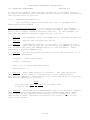
Sol
SYSTEMS
MANUAL,
6200 Hollis Street
Emeryville, CA. 94608
Phone: (415) 652-8080
Copyright 1976,
1977, Processor Technology
Third Printing, June, 1977
Manual No.106000
Corporation
PREFACE
This new edition of the Sol Systems Manual contains many
revisions and additions. Its release coincides with the release
of a new "2708" Personality Module, and the Revision E version
of the main circuit board: Sol-PC. The new "Sol-PC Rev E" has
several improvements: resistors have been added which increase
the reliability of the cassette motor relays, jumper options have
been added, and traces moved to improve performance. Many
improvements which had been accumulating as update information
have been integrated into the text. Section VII, Operating
Procedures, and Appendix 5, IC Pin Configurations, are now
included. A subsection, Modification for 625 Line Video, has
been added. If your copy is missing Section VIII, Theory of
Operation, it will be available soon. New divider pages with
plastic-coated tabs are included to make it easier to flip to
frequently referenced sections.
Much effort has gone towards making this manual complete
and accurate. The process of updating and revision always
continues, however, and we invite your input. If you should
find an error, or have suggestions for improving any of our
documentation, please submit your suggestions in writing to our
Technical Documentation Department, and they will be given
thorough consideration.
The three-ring binder you are holding, is an "easel" binder.
The cover is hinged from side to side, as well as down the binding, so that it may form its own "easel" stand. To use this
feature, lay the manual open on a table. Bend the full width of
the manual along the creased hinge, until a resistance to further
bending is felt. Then set the manual up on the table, with the
bottom of the pages down against the table, and the top inclining
away from you. It is supported from falling by the portion of
the binder you have bent back. In this position your hands are
free for building, making measurements, or troubleshooting.
The first part of this manual you should read is at the
very end: the Updates section. Integrate this information into
your manual before you begin.
CONTENTS OUTILNE
Detailed contents precede each section.
I
INTRODUCTION and GENERAL INFORMATION
II
Sol POWER SUPPLY ASSEMBLY and TEST
III
Sol-PC ASSEMBLY and TEST
IV
PERSONALITY MODULE ASSEMBLY
V
KEYBOARD ASSEMBLY and TEST
VI
Sol CABINET-CHASSIS ASSEMBLY
VII
OPERATING PROCEDURES
VIII THEORY OF OPERATION
IX
SOFTWARE
X
DRAWINGS
APPENDICES
UPDATES
PROCESSOR
Sol TERMINAL COMPUTER
TECHNOLOGY
TM
CORPORATION
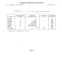
LIST OF ILLUSTRATIONS
TITLE
PAGE
2-1
2-2
2-3
2-4
2-5
2-6
2-7
sol-20 fan closure plate assembly . . . . . . . .
Coaxial cable preparation . . . . . . . . . . . .
Aluminum heat sink installation . . . . . . . . .
Sol-10 power supply subchassis assembly . . . . .
Sol-20 power supply subchassis assembly . . . . .
Sol-PC power connector and voltage measurements .
Sol-20 power connector and voltage measurements .
II-7
II-9
II-12
II-15
II-16
II-19
II-19
3-1
3-2
3-3
3-4
3-5
3-6
3-7
3-8
3-9
3-10
3-11
Identification of components . . . . . . . . . .
Clock circuit waveforms . . . . . . . . . . . . .
Test probe for Steps 16B and 25B . . . . . . . .
Coaxial cable preparation . . . . . . . . . . . .
Display section timing waveforms . . . . . . . .
Bending selected pins on U42, 59 and 75 . . . . .
U14 through U21 socket jumpers . . . . . . . . .
Display circuits test pattern . . . . . . . . . .
CPU Functional Test No. 1 display . . . . . . . .
CPU Functional Test No. 2 display . . . . . . . .
Personality module bracket/guide installation . .
III-5
III-15
III-16
III-19
III-21
III-23
III-24
III-25
III-29
III-31
III-31
4-l
4-2
R1 through R4 installation . . . . . . . . . . .
Handle bracket (Sol-1045) installation . . . . .
IV-4
IV-5
6-l
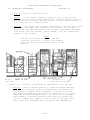
Types of screws used in Sol cabinet-chassis
. . . . . . . . . . . . . . . . . . . .
assembly
Brackets used in Sol cabinet-chassis assembly . .
Sol-20 with covers removed . . . . . . . . . . .
Sol-20 with covers removed . . . . . . . . . . .
Sol-PC coaxial cable connector assembly . . . . .
Backplane board (Sol-BPB) installation . . . . .
Backplane board (Sol-BPB) installation . . . . .
Protective foot pad installation . . . . . . . .
VI-4
VI-4
VI-11
VI-11
VI-14
VI-16
VI-17
VI-20
FIGURE
6-2
6-3
6-4
6-5
6-6
6-7
6-8
7-l
7-2
7-3
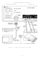
Connecting the basic Sol system . . . . . . . . . VII-6
Sol control switch settings for terminal mode . .
VII-7
Location Of positioning adjustments, VR1 and VR2
VII-8
PROCESSOR
TECHNOLOGY
CORPORATION
Sol TERMINAL COMPUTERTM
TABLE
PAGE
TITLE
FIGURE
7-5
7-6
7-7
7-8
ILLUSTRATIONS/TABLES
Connecting
Connecting
Connecting
Connecting
Sol
Sol
Sol
Sol
to two
SDI to
SDI to
PDI to
cassette recorders . . .
current loop device such
communications modem . .
parallel device . . . .
. . . .
as TTY
. . . .
. . .
TITLE
VII-29
VII-31
VII-31
VII-32
PAGE
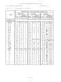
2-1 Sol Regulator Parts List . . . . . . . . . . . . . . . .
2-2 Sol-10 Power Supply Parts List . . . . . . . . . . . . .
2-3 Sol-20 Power Supply Parts List . . . . . . . . . . . . .
II-2,3
II-4
II-4
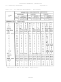
3-1
Sol-PC Parts List . . . . . . . . . . . . . . . . . .
III-2,3,4
4-1
PM2708 Personality Module Parts List
IV-1
5-1
Sol Keyboard Parts List . . . . . . . . . . . . . . .
V-2,3
6-l
6-2
Sol-10 Cabinet-Chassis Parts List . . . . . . . . . .
Sol-20 Cabinet-Chassis Parts List . . . . . . . . . .
VI-2
VI-3
7-l
7-2
7-3
7-4
7-5
Sol Operating Controls and Their Functions . . . . .
Baud Rate Selection with Switch S3 . . . . . . . . .
VII-2
VII-15
Word Length Selection with S4-2 & 3
. . . . . . . .
Sol Keyboard Assignments . . . . . . . . . . . . . .
Control Character Symbols and Definitions . . . . . .
VII-15
VII-18
VII-23
. . . . . . . .
I
INTRODUCTION and GENERAL INFORMATION
1.1
Introduction . . . . . . . . . . . . . . . .
I-1
1.2
General Information
I-2
1.2.1
1.2.2
1.2.3
1.2.4
1.2.5
. . . . . . . . . . . .
Sol-PC Description .
Receiving Inspection
Warranty Information
Replacement Parts .
Factory Service . .
.
.
.
.
.
.
.
.
.
.
.
.
.
.
.
.
.
.
.
.
.
.
.
.
.
.
.
.
.
.
.
.
.
.
.
I-1
I-2
I-2
I-2
I-2
PROCESSOR
TECHNOLOGY CORPORATION
Sol-PC SINGLE BOARD TERMINAL COMPUTERTM
1.1
SECTION I
INTRODUCTION
This manual supplies the information needed to assemble,
test and use the Sol-PC Single Board Terminal Computer. We suggest
that you first scan the entire manual before starting assembly.
Then make sure you have all the parts and components listed in the
"Parts List" (Table 3-l) in Section III. When assembling the module,
follow the instructions in the order given.
Should you encounter any problem during assembly, call on us
for help if necessary.
If your completed module does not work properly , recheck your assembly step by step. Most problems stem from
poor soldering, backward installed components, and/or installing
the wrong component. Once you are satisfied that the module is correctly assembled, feel free to ask for our help.
1.2
GENERAL
1.2.1
Sol-PC
INFORMATION
Description
The Sol-PC is a single board microcomputer/terminal built
around an 8080 microprocessor.
Support circuitry permits full implementation of every 8080 function.
It features both parallel and serial communications interfaces, a keyboard interface, an audio cassette interface, a video
display generator, 1024 8-bit words of system RAM (random access
memory), 1024 8-bit words of display RAM, and a plug-in personality
module with up to 2048 bytes of ROM (read only memory) stored program, and bus compatibility with all Processor Technology hardware
Power requirements for the Sol-PC are + 5 V
and firmware products.
dc +-5% at 2.5 A, +12 V dc +-5% at 150 mA and -12 V dc +-5% at 200 mA.
Parallel interfacing is eight bits each for input and output
plus control handshaking signals, and the output bus is tristated
TTL for bidirectional interfaces. The serial interface circuit includes both asynchronous RS-232 and 20 mA current loop provisions,
75 to 9600 baud (switch selectable).
Seven-level ASCII encoded, TTL keyboard interfacing requires a 2 to 10 usec strobe pulse after data is stable. The dual
rate, 300 or 1200 bps (bits per second), audio cassette interface is
program controlled and self clocking with phase-lock loop. It
includes automatic level control in both the record and playback
modes.
Recording is CUTS/Byte standard compatible, asynchronously
Manchester coded at 1200/2400 Hz or 600/1200 Hz.
The video display circuitry generates sixteen 64 character
lines from data stored in an on-card 1024 8-bit word display RAM.
Alphanumeric and control characters (the full 128 upper and lower
case plus control ASCII character set) are displayed black on white
I-l
PROCESSOR
Sol-PC SINGLE BOARD TERMINAL
TECHNOLOGY
CORPORATION
COMPUTERTM
SECTION I
Solid video inversion cursors, with
or reverse (switch selectable).
switch selectable blink, are programmable. The display output is
standard EIA, 1.0 to 2.5 V p-p with composite negative sync, with a
nominal bandwidth of 7 MHz.
It can consequently be used to drive any
standard video monitor.
(A monochrome TV, converted for video input,
can also be used.
See Appendix VI.)
Included on the card are 1024 words of static, low power system RAM capable of full speed operation and a plug-in personality
module which contains the software control program. Three personality
modules are available for Sol:
CONSOLTM --allows simple terminal operations plus
direct control of the basic computer functions for
entering or examining data in any memory location,
or executing a program stored at a known location
in memory.
SOLEDTM --allows advanced terminal operations with
CONSOL plus screen, file and cassette tape editing/
transmission operations.
SOLOSTM --allows
operation.
1.2.2
Receiving
full
stand-alone
terminal-computer
Inspection
When your kit arrives, examine the shipping container for
signs of possible damage to the contents during transit.
Then inspect the contents for damage.
(We suggest you save the shipping
materials for use in returning the kit to Processor Technology
should it become necessary to do so.)
If your Sol-PC kit is damaged,
please write us at once describing the condition so that we can take
appropriate action.
1.2.3
Warranty
Information
In brief, parts which fail because of defects in materials or
workmanship are replaced at no charge for 3 months for kits, and one
year for assembled products, following the date of purchase. Also,
products assembled by the buyer are warranted for a period of 3
months after the date of purchase; factory assembled units carry a
one year warranty. Refer to Appendix I for the complete "Statement
of Warranty".
1.2.4
Replacement
Parts
Order replacement parts by component nomenclature (DM8131 IC
or lN2222 diode, for example) and/or a complete description (680 ohm,
1/4 watt, 5% carbon resistor, for example).
I-2
PROCESSOR
TECHNOLOGY
CORPORATION
Sol-PC SINGLE BOARD TERMINAL COMPUTERTM
1.2.5
SECTION I
Factory Service
In addition to in-warranty service, Processor Technology also
provides factory repair service on out-of-warranty Processor Technology products. Before returning the unit to us, first obtain our
authorization to do so by writing us a letter describing the problem.
After you receive our authorization to return the unit, proceed as
follows:
1.
Write a description of the problem.
2.
Pack the unit with the description in a container
suitable to the method of shipment.
3 . Ship prepaid to Processor Technology Corporation,
6200 Hollis Street, Emeryville, CA 94608.
Your unit will be repaired as soon as possible after receipt
and return shipped to you prepaid.
(Factory service charges will not
exceed $20.00 without prior notification and your approval.)
I-3
II
Sol POWER SUPPLY ASSEMBLY and TEST
2.1
Introduction . . . . . . . . . . . . . . . .
II-1
2.2
Parts and Components . . . . . . . . . . . .
II-1
2.2.1
2.2.2
Sol Regulator (Sol-REG) . . . . .
Power Supply Subchassis and
Components . . . . . . . . . . . .
II-1
Assembly Tips. . . . . . . . . . . . . . . .
II-5
2.3.1
2.3.2
Electrical . . . . . . . . . . . .
Mechanical . . . . . . . . . . . .
II-5
II-5
2.4
Assembly Precautions . . . . . . . . . . . .
11-5
2.5
Required Tools, Equipment and Materials
. .
II-6
2.6
Orientation
. . . . . . . . . . . . . . . .
II-6
Sol-REG PC Board . . . . . . . . .
Fan Closure Plate . . . . . . . .
II-6
II-6
2.3
2.6.1
2.6.2
2.7
Assembly-Test
2.7.1
2.7.2
2.7.3
. . . . . . . . . . . . . . .
Fan Closure Plate Assembly . . . .
Sol-REG Assembly and Test . . . .
Power Supply Subchassis Assembly
and Test . . . . . . . . . . . . .
II-2
II-6
II-7
II-10
II-14
PROCESSOR
TECHNOLOGY
CORPORATION
SECTION II
Sol POWER SUPPLY
2.1
INTRODUCTION
The Sol power supply consists of a regulator board plus additional chassis-mounted components. This section covers assembly
and test of the complete power supply.
2.2
PARTS AND COMPONENTS
2.2.1
Sol Regulator (Sol-REG)
Check all parts and components against the appropriate
"Parts List", Tables 2-1, 2-2 and 2-3.
If you have difficulty in
identifying any parts by sight, refer to Figure 3-1 on Page III-5
in Section III of this manual.
2.2.2
Power Supply Subchassis and Components
In addition to the Sol-REG, you will need the following
parts and components supplied with the Sol Cabinet-Chassis Kit.
Check these parts against the appropriate "Parts List(s)", Tables
6-l and 6-2, in Section VI and separate them from the other cabinetchassis parts.
Fan Closure Plate
Power Supply Subchassis (L-shaped)
4 each 4-40 x 3/16 Machine Screw
4 each 4-40 x 5/16 Machine Screw
4 each 4-40 Hex Nut
10 each #4 Lockwasher
14 each 6-32 x 1/2 Machine Screw
14 each 6-32 Hex Nut
16
3
3
3
11
each
each
each
each
each
#6 Lockwasher
8-32 x 1/2 Machine Screw
8-32 Hex Nut
#8 Lockwasher
#6 x 1/4 Sheet Metal Screw
1 each #6 x 5/16 Sheet Metal Screw
2 each #4 Solder Lug
2 each 1/4" Spacer, 4-40 Tapped
Rev A
II-1
PROCESSOR
TECHNOLOGY
CORPORATION
Sol POWER SUPPLY
SECTION II
Table 2-1.
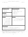
INTEGRATED
1
1
1
Sol Regulator Parts List.
CIRCUITS**
DIODES and RECTIFIERS
1458 (U2)
7812 (U1)
7912 (U3)
1
1
1
MDA101A (FWB2)
MDA970-1 (FWB1)
IR106B2 or MCR106-2 (SCR1)
2 1N4001 (D3 & 4)
TRANSISTORS
1 1N4148 (D2)
1 1N5231B (D1)
2 2N2222 (Q2 & 3)
1 T1P41 (Q1)
RESISTORS
1
1
1
2
4
1
1
1
ohm,
or
68
ohm,
330
ohm,
1 K ohm,
10 K ohm,
56 K ohm,
1690
ohm,
4020
ohm,
CABLE
0.1
CAPACITORS
3 watt,
5 watt,
1/4 watt,
1/4 watt,
1/4 watt,
1/4 watt,
1/4 watt,
1/4 watt,
1/4 watt,
5%
5%
5%
5%
5%
5%
5%
5%
5%
2
3
.1 ufd, disc
15
ufd, tantalum dipped
2
2500
ufd, tubular electrolytic
1 "18,000
ufd, electrolytic
ASSEMBLIES
1 *Single wire, 3" (Fuse Holder to Power Switch)
1 *Single wire, 3 1/4 (Power Switch to Commoning Block)
1 Two wire, 10" (C8 to Regulator Board)
*Chassis-mounted component
**When identifying IC's, you can iqnore prefix and suffix characters
in the IC nomenclature since these vary with the manufacturer.
For
example a 1458CP, 1458CPI and MC1458N are all 1458 IC's.
This
applies to all Parts Lists in this manual.
II-2
PROCESSOR
TECHNOLOGY
CORPORATION
SECTION II
Sol POWER SUPPLY
Table 2-1.
Sol Regulator Parts List (Continued).
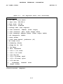
MISCELLANEOUS
1 Sol REG Circuit Board
1 Heat Sink, 690-220-P
1 Heat Sink, 203-AP
1 Heat Sink, aluminum
1 Package Heat Sink Compound
2 Coax Connector, female* (Video Output)
1
1
1
1
1
Coax Connector, male (Video Output Cable)
Coax Connector Adapter Sleeve (Video Output Cable)
*AC Receptacle, female
*Fuse Holder
*SPST Power Switch, pushbutton (S5)
1
2
1
4
3
1
1
2
1
2
3
5
1
AC Power Cord
*Commoning Blocks
*Clamp for C8, 11/2"
Tie Wraps
Mica Insulators
4-40 x 7/16 screw
4-40 x 5/8 screw
4-40 Hex Nut
6-32 x 1/2 screw, metal
6-32 x 1/2 screw, Nylon
6-32 Hex Nut
#4 Lockwasher, internal tooth
Length Solder
*Chassis-mounted
component
II-3
PROCESSOR
TECHNOLOGY
CORPORATION
SECTION II
Sol POWER SUPPLY
Table 2-2.
Sol-10 Power Supply Parts List.
The Sol-10 Power Supply Kit includes all Sol-REG parts listed in
Table 2-l plus the following components:
.__-_--------------------------------------------------------------.
1 *Power Transformer, T1
1 *Fuse, 3 amp Slo-Blo (F1)
*Chassis-mounted
component
Table 2-3.
Sol-20 Power Supply Parts List.
The Sol-20 Power Supply Kit includes all Sol-REG parts listed in
Table 2-l plus the following components:
,------------------_---------------------------------------------
RESISTORS
CAPACITORS
1 *39 ohm, 2 watt, 5%
RECTIFIERS
1 *54,000 ufd, electrolytic
TRANSFORMERS
1 *MDA980-1 (FWB3)
1 *Power Transformer, T2
MISCELLANEOUS
1 *Fan
1 *Fan Guard
1 *Fuse,
3
amp Slo-Blo
*Chassis-mounted
1 5-wire Cable Assembly
1 *Clamp for C9, 21/2"
2 *#l0 solder lug, internal tooth
component
II-4
PROCESSOR
TECHNOLOGY
SECTION II
Sol POWER SUPPLY
2.3
ASSEMBLY TIPS
2.3.1
Electrical
CORPORATION
For the most part the assembly tips given in Paragraph 3.2
of Section III (Page III-l) apply to assembling the Sol regulator
board and power supply.
In addition, scan Section II completely before you start to
assemble the power supply.
2.3.2
Mechanical
1.
If you do not have the proper screwdrivers (see Paragraph 2.5), we recommend that you buy them rather than using a knife
point, a blade screwdriver on a Phillips screw, and other makeshift
means. Proper screwdrivers minimize the chances of stripping
threads, disfiguring screw heads and marring decorative surfaces.
2.
To assure a correct fit and tight assembly, be sure you
use the screws specified in the instructions.
3.
Lockwashers are widely used in the power supply assembly
so that screws will not loosen when subjected to stress or vibration.
When a lockwasher is specified, do not omit it and make sure you
install it correctly.
4. Some instructions call for prethreading holes. This is
done to make assembly easier by giving you maximum working space for
installing relatively hard-to-drive sheet metal screws. If you bypass prethreading instructions you will only make subsequent
cabinet-chassis assembly more difficult.
To prethread a hole, insert specified screw in the hole
and position it as straight as possible. While holding the screw in
this position, drive it into the metal with the proper screwdriver.
If started straight the screw will continue to go straight into the
metal so that the head and sheet metal surfaces are in full contact.
5.
The diameter of the shank (threaded portion) of a screw
increases in relation to its number. For example, a 6-32 screw is
larger in diameter than a 4-40 screw. Also, a #8 lockwasher is
larger than a #4 lockwasher.
6.
Heat sink compound is supplied with this kit in a small
clear plastic package. It is a thick white substance which improves
transfer between components and their heat sinks. To use
the compound, pierce a small hole near the edge of the top surface
of the plastic package, using a pin or sharp knife point. Squeezing
the package will cause a small amount of the compound to ooze out
Rev B
II-5
PROCESSOR
TECHNOLOGY
CORPORATION
SECTION II
Sol POWER SUPPLY
out of the hole, which may then be applied with a toothpick or small
screwdriver blade. Spread a thin film of the compound on the mating
surfaces of both the heat-generating component and the heat sink
surface which it will contact. Then assemble as directed.
2.4
ASSEMBLY
PRECAUTIONS
The precautions concerning soldering and the installation
and removal of integrated circuits given in Paragraph 3.3 of Section
III (Page 111-6) also apply to assembling the Sol regulator board.
2.5
REQUIRED TOOLS, EQUIPMENT AND MATERIALS
The following tools, equipment and materials are recommended
for assembling the Sol regulator board:
1.
2.
3.
4.
5.
6.
7.
8.
9.
Needle nose pliers
Diagonal cutters
Sharp knife
Screwdriver, thin 1/4" blade
Screwdriver, #2 Phillips
Controlled heat soldering iron, 25 watt
60-40 rosin-core solder (supplied)
Volt-ohm meter
Ruler
2.6
ORIENTATION
2.6.1
Sol-REG PC Board
Location C5 (2500 ufd capacitor) will be located in the lower
right-hand corner of the circuit board when locations SCR1, Q1 and
FWB1 are positioned along the top of the board. In this position
the component (front) side of the board is facing up and the
horizontal legends will read from left to right; the other legends
will read from bottom to top. Subsequent position references
related to the Sol-REG board assume this orientation.
2.6.2
Fan Closure Plate
The large circular cutout will be located in the upper right
quadrant of the plate when the heavy guage doubler plate is facing
UP. In this position the rectangular cutouts are on the left, the
front side of the plate is facing down, the back side is facing up,
you
and the small circular cutout is
- at- the- bottom. We suggest
2.7
Rev B
ASSEMBLY-TEST
NOTE: Instructions that apply only to the Sol-20 are
preceded by an asterisk. Skip these instructions
if you are assembling a Sol-lo.
II-6
PROCESSOR TECHNOLOGY CORPORATION
Sol POWER SUPPLY
2.7.1
SECTION II
Fan Closure Plate Assembly
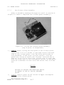
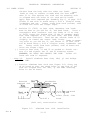
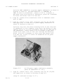
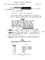
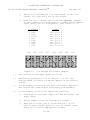
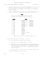
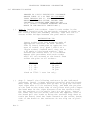
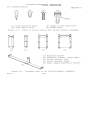
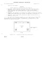
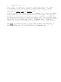
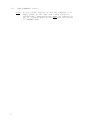
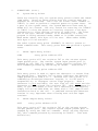
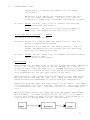
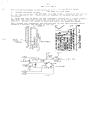
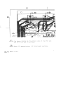
Refer to Assembly Drawings dn Pages X-1 and 2 in Section X.
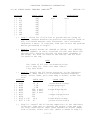
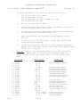
(Figure 2—1 shows a completed fan closure plate assembly.)
Figure 2—1. Sol-20 fan closure plate assembly.
(Top of plate in foreground.)
*( ) Step 1. Mount cooling fan and guard to fan closure plate.
Insert four 6—32 x ½” binder or pan head screws from back
side of fan closure plate. (Use the holes positioned in
each quandrant of the large circular cutout.) Slip fan
guard over screws on front side of plate. Position fan so
that air flow will be from front to back side of plate and
with its leads next to the rectangular cutouts in the place.
Place #6 lockwasher on each screw and secure with 6—32 hex
nut.
WARNING
FAILURE TO INSTALL FAN GUARD MAY RESULT
IN DAMAGE TO THE Sol AND/OR PERSONAL
INJURY.
( )
ReVB
Step 2. Install power on-off switch in upper rectangular
cutout in fan closure plate.
(Step 2 continued on Page il-S.)
11—7
PROCESSOR
TECHNOLOGY
CORPORATION
SECTION II
Sol POWER SUPPLY
Bend four retainer tabs on switch in and position switch
with terminals facing front side of fan closure plate. Push
switch unit from back side of plate through mounting hole
and bend retainer tabs outward if needed to hold switch in
place.
( ) Step 3. Install commoning blocks (Item 6 on drawing on Page
X-l) on front side of fan closure plate, one on each side of
on-off switch.
Position each block with terminal #1 at top and terminal #5
at bottom and attach each block to front side of fan closure
Insert
plate with two 6-32 X 1/2 binder or pan head screws.
screws from back side of plate, place block over screws, on
front side of plate, put #6 lockwasher on each screw and
secure with 6-32 hex nut.
( ) Step 4. Install fuse holder in mounting hole located between
the two rectangular cutouts in the fan closure plate.
Insert fuse holder from back side of plate, poition large
tab at top, next to on-off switch,and secure holder to plate
with the large lockwasher and nut supplied with holder.
( ) Step 5. Install AC Power cord receptacle on fan closure
plate.
Position receptacle on front side of fan closure plate over
the rectangular cutout below fuse holder. Orient receptacle
with green lead at the botton and align the receptacle and
closure plate mounting holes. Insert two 6-32 x 1/2 binder or
pan head screws from back side of plate through each mounting hole, put #6 lockwasher on each screw and secure with
6-32 hex nut. Be sure receptacle is properly seated in cutout before tightening to avoid damage.
( ) Step 6.Install female coaxial connector on fan closure plate.
Insert connector from front side of plate so that the threaded
end projects through to the back side. Then insert four 4-40
X 5/16 binder or pan head screws from back side of plate
through the four connector and plate mounting holes. Place #4
lockwasher on each screw except the upper one which is closest
to the
(Leave
- AC
- receptacle. Secure with 4-40 hex nuts.
upper nut closest to receptacle loose.)
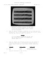
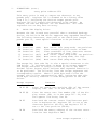
( ) Step 7.
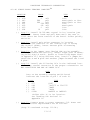
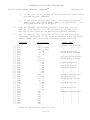
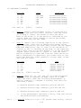
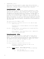
Prepare RG59/U coaxial cable.
Cut a 13" piece of coaxial cable from that supplied with the
Sol-PC kit. Strip away one inch of the outer insulation at
both ends to expose shield. Unbraid shield at one end and
twist it into a single lead. Do the same thing at the other
end. Tin shield lead at each end and solder a #4
lug to each lead. Then remove 1/2" of the inner conductor
insulation at both ends.
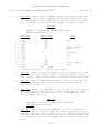
(See Figure 2-2.)
Rev B
II-8
PROCESSOR
TECHNOLOGY
CORPORATION
SECTION II
Sol POWER SUPPLY
Figure 2-2.
Coaxial cable preparation.
( ) Step 8. Connect coaxial cable to coaxial connector installed in Step 6.
Solder inner conductor on one end to the pin of the connector. Remove hex nut on upper connector mounting Screw
closest to AC receptacle, place lug (coaxial shield) on
screw and reinstall hex nut.
( ) Step 9.
Connect fan closure plate wiring.
( ) Install the 3" power switch-to-commoning block cable
supplied with your Sol-REG kit. Connect the female
spade lug end to the upper terminal of the on-off switch
and the commoning block lug end to the #1 terminal of
the commoning block closest to the fan. NOTE: To install
commoning block lugs, position lug with its open side
facing away from the terminal numbers on the block. Then
gently push lug into appropriate terminal receptacle until
it is fully seated.
( ) Install the 3 1/4" fuse holder-to-power switch cable supplied with your Sol-REG kit.
(This cable has female
spade lugs at both ends.) Connect one end to the bottom
terminal of the on-off switch and the other to the
longer male spade lug on the fuse holder.
( ) Connect the AC receptacle wire closest to the fan to the
other fuse holder lug. NOTE: The green AC receptacle
wire will be connected later.
( ) Connect other AC receptacle wire to terminal #4 on the
commoning block furthest away from the fan.
*( ) Connect upper wire of fan cord to terminal #3 of the
commoning block closest to fan.
*( ) Connect lower wire of fan cord to terminal #5 of commoning block furthest from fan.
( ) Put fan closure assembly aside.
II-9
Rev B
PROCESSOR
TECHNOLOGY
CORPORATION
SECTION II
Sol POWER SUPPLY
2.7.2
Sol-REG Assembly and Test
Circuit references, values and outlines are printed on the
component side of the board to assist in assembly.
( ) Step 10. Visually check Sol-REG board for solder bridges
(shorts) between traces, broken traces and similar defects.
If visual inspection reveals any defects, return the board
to Processor Technology for replacement. If the board is
not defective, proceed to next paragraph.
( ) Step 11. Install the following resistors in the indicated
locations. Bend leads to fit distance between mounting
holes, insert leads, pull down snug to board, solder and
trim.
LOCATION
R1
R2
R3
R4
R5
R6
R7
R8
R9
R10
R11
R12
VALUE
.1,
330
10
10
1
68
10
1
56
10
1690
4020
(ohms)
3 watt
5 watt
K
K
K
K
K
K
K
COLOR CODE
none
orange-orange-brown
brown-black-orange
"
"
"
brown-black-red
blue-gray-black
brown-black-orange
brown-black-red
green-blue-orange
brown-black-orange
bronw-blue-white-brown
yellow-black-red-brown
step 12. Install U2 (1458) in its location between C2 and C3.
U2 is positioned with pin 1 in the lower left-hand corner and
soldered into place. See "Loading DIP Devices" in Appendix IV.
Step 13. Install diodes D1
Bend leads to fit
(1N4001).
insert leads, pull down snug
SURE to position D1 with its
D2 and D3 with their cathode
cathode at the top.
(1N5231B), D2 (1N4148), D3 and D4
distance between mounting holes,
to board, solder and trim. BE
cathode (dark band) to the left,
at the bottom, and D4 with its
( ) Step 14. Install the following capacitors in the indicated
locations. Take care to observe the proper value, type and
orientation, if applicable, for each installation. Bend
leads outward on solder (back) side of board, solder and
trim.
(See NOTE on Page 11-11.
II-10
Rev B
PROCESSOR
TECHNOLOGY
CORPORATION
SECTION II
Sol POWER SUPPLY
NOTE
Disc capacitor leads are usually coated
with wax during the manufacturing proAfter inserting leads through
cess.
mounting holes, remove capacitor and
clear the holes of' any wax. Reinsert
and install.
LOCATION
- C1
C2
C3
C6
C7
VALUE (ufd)
15
.1
.1
15
15
TYPE-
ORIENTATION
Tantalum
Disc
Disc
Tantalum
Tantalum
"+" lead bottom right
None
None
"+" lead right
"+" lead left
Step 15.
Install 2500 ufd capacitors in locations C4 and
C5.
Bend leads to fit distance between mounting holes,
Be
insert leads, pull down snug to board, solder and trim.
sure to install C4 with its "+" lead to the right and C5
with its " + " lead to the left.
Install Q2 and Q3 (2N2222) in their locations.
step 16.
The emitter lead (closest to tab on can) of Q2 is oriented
toward the left and the base lead toward the bottom. The
emitter lead of Q3 is oriented toward the bottom and the
base lead toward the right.
Step 17.
Read assembly tip 6, on page 11-5.
Apply heat
sink compound to the inside of the small black "starshaped" cooling fin, and install it, with the cylinderical
grip down, on Q2 by slipping it down onto the can. Be
sure heat sink does not touch any other component on the
board.
Step 18.
Install bridge rectifier FWB 2 (MDA1O1A) in its
location at the bottom of the board.
Apply heat sink
compound, per Assembly tip 6 on page 11-5. Position FWB2
with its "+" lead at the top and its "-" lead at the bottom,
insert leads, solder and trim.
Step 19.
Install large heat sink, U1 and U3 in their locations on the bottom left corner of the circuit board.
( ) Position large black heat sink, (flat side to board) over
the square foil area in the lower left corner of the PC
board. Orient sink so that the two triangular cutouts in
the sink are over the two triangles of mounting holes in
the board.
Rev B
( ) Position U1 (7812) on heat sink and observe how leads must
be bent to fit mounting holes. Note that the center lead
must be bent down approximately 0.2 inches.
II-11
PROCESSOR
TECHNOLOGY
CORPORATION
Sol POWER SUPPLY
SECTION II
further from the body than the other two leads. Bend
leads so that no contact is made with the heat sink
when Ul is flat against the sink and its mounting hole
is aligned with the holes in the sink and PC board.
Apply heat sink compound per Assembly Tip 6, on page 11-5.
Fasten U1 and sink to board using a 6-32 x 1/2 metal screw,
lockwasher and nut.
Insert screw from back (solder) side
of board and drive nut finger tight.
( ) Position U3 (7912) on heat sink, determine how leads
must be bent as you did for U1, and bend leads.
Place a
rectangular mica insulator over the leads of U3 so that
it fully covers the bottom side of the U3 package. Apply
heat sink compound to U3, the heat sink, and both sides
of the mica insulator.
Bend the two outside leads of U3
slightly in toward the center lead, insert leads in mounting holes as you did for U1, and fasten U3 to heat sink
and PC board using a 6-32 x 1/2 Nylon screw, lockwasher and
nut.
Insert screw from back (solder) side of board and
drive nut finger tight.
( ) Position heat sink, U1 and U3 as needed to obtain correct fit and tighten the U1 and U3 mounting screws.
REMEMBER, NO LEADS CAN CONTACT THE SINK. Solder all
leads and trim if required.
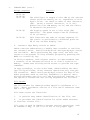
( ) Step 20.
Install aluminum heat sink, SCR1, Q1 and bridge
rectifier EWB1.
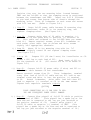
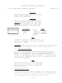
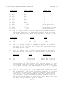
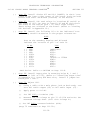
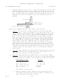
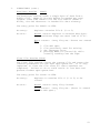
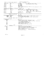
( ) Position aluminum heat sink (see Figure 2-3) along top
of PC board so that the three holes in one side of the
sink are aligned with the SCR1, Q1 and FWB1 mounting
holes in the PC board.
Lockwasher
Heatsink
Compound and
Insulator
ePC Board
Solder (back) Side
4-40 x 7/16 Screw
(Left end, cross-section view)
Figure 2-3.
Rev
B
Aluminum heat sink installation.
II-12
PROCESSOR
TECHNOLOGY
CORPORATION
SECTION II
Sol POWER SUPPLY
( ) Position Q1 (TIP41), with component nomenclature up, on
heat sink so hole in Q1 package is aligned with the holes
in sink and PC board. Observe how the leads of Q1 must
be bent down to fit the pads for Q1 and bend them accordingly. Apply heat sink compound to Q1, the heat sink,
and both sides of the rectangular mica insulator. Place
mica insulator between heat sink and Q1, insert leads
(emitter lead to right) and fasten Q1, insulator and heat
sink to board with a 6-32 x 1/2 Nylon screw, lockwasher
and nut. Insert screw from back (solder) side of board
and drive nut finger tight.
( ) Position FWB1 (MDA970-1), with "+" lead to the right, on
heat sink, determine how leads must be bent as you did
for Q1, and bend leads. Apply heat sink compound. Insert
leads ("+" lead to right) and fasten FWB1 and heat sink
to PC board with a 4-40 x 5/8 screw, lockwasher and nut.
Insert screw from back (solder) side of board and drive
nut finger tight.
( ) Position SCR1 (IR106B2 or MCR106-2) on heat sink with
component nomenclature up and prepare it for installation as you did Q1 and FWB1.
Apply heat sink compound
to SCR1, the heat sink, and both sides of the circular
mica insulator. Place the mica insulator between the heat
sink and SCR1, insert leads and fasten SCR1, insulator and
heat sink to PC board with a 4-40 x 7/16" screw, lockwasher
and nut. Insert screw from back (solder) side of board and
drive nut finger tight.
( ) Check alignment of heat sink, SCR1, Q 1 and FWB2 and
tighten the three mounting screws. Solder all leads
and trim if required. Wipe off excess heat sink compound,
if necessary. NOTE: The heat sink may have to be
repositioned when you mount the Sol-REG on the power
supply subchassis. This will require that you loosen the
mounting screws for SCR1, Q1 and FWB2 and retighten them
after repositioning the heat sink.
( ) Step
21.
Connect two wire cable assembly (C8 to Regulator
Board cable) to regulator. Tin ends without lugs and solder
green (+) lead to pad X2 and white (-) lead to pad X3.
Test Sol-REG for short circuits. Check for continuity between FWB1 (MDA970-1) mounting screw and the following points:
(The resistance should be greater than 20 ohms
in all cases.)
D3, top lead
x2
Q1, Base
T2
Q1, Collector
D4, top lead
T1
D1, right-hand lead
*D3, bottom lead
*D4, bottom lead
Q1, Emitter
R1, left-hand lead
*Resistance will be initially low due to C4 and C5, but it
should increase to greater than 20 ohms after a few seconds.
( ) Step 22.
Rev B
II-13
PROCESSOR
TECHNOLOGY
CORPORATION
SECTION II
Sol POWER SUPPLY
( ) Step 23.
2.7.3
Set Sol-REG to one side.
Power Supply Subchassis Assembly and Test
( ) Step 24. Mount transformer (T1 for Sol-lo, T2 for Sol-20) on
power supply subchassis (L-shaped chassis).
Position transformer as shown in drawing on Page X-2 and attach
it to the subchassis with three 8-32 x 1/2 binder or pan head
screws, #8 lockwashers and 8-32 hex nuts. Insert screws from
bottom and outer side of chassis as shown. Place lockwasher
on each screw and secure loosely with hex nuts. Slide transformer as close as possible to the edge of the chassis and
tighten nuts.
NOTE
- Only one of the holes in the side wall is
used. Use the one that lines up with the
transformer mounting tab.
( ) Step 25.
Prepare transformer leads.
( ) Twist the two black wires together except for the last
two inches at the commoning block lug end.
( ) Twist the two green wires together for their full length.
( ) Twist the two yellow wires together for their full
length.
*( ) Twist the two blue wires together for their full length.
Connect Sol-PC power cable (4-wire cable which
connects to J10 on Sol-PC) to Sol-REG. Tin ends of cable
and solder green lead to pad X9, white lead to pad X1, red
lead to pad X7 and white-yellow lead to pad X8.
( ) Step 26.
*( ) Step 27.
Connect Sol-20 DC power cable (5 wire) to Sol-REG.
Tin ends of cable and solder white lead to pad X4 (above R8),
red-white lead to pad X5 (between C5 and F W B 2 ) and yellowwhite lead to pad X6 (left of C5).
( ) Step 28.
Connect
transformer leads to Sol-REG.
( ) Solder green leads to pads T1 and T2, white-yellow lead
to pad T3 and yellow leads to pads T4 and T5 on Sol-REG
circuit board.
( ) Step 29.
Prethread the three Sol-REG heat sink mounting
holes in the power supply subchassis shown in drawing on
page X-2 with #6 x 5/16 sheet metal screws. Remove screws.
Rev
B
II-14
PROCESSOR TECHNOLOGY CORPORATION
Sol POWER SUPPLY
SECTION II
( )
Step 30. Place #4 lockwashers on two 4-40 x 3/16 binder or
pan head screws. Insert these screws from the bottom side
of the power supply subchassis through the two mounting holes
located near the middle of the bottom of the power supply
subchassis, one on each side. Place another *4 lockwasher
on the screws and drive each screw tightly into a 4—40 x ¼
tapped spacer.
( )
Step 31. Position Sol—REG PC board with top edge over the
previously installed spacers. Place #4 lockwashers on two
4—40 x 3/16 binder or pan head screws and drive screws t
through Sol-REG board into spacers.
( )
Step 32. Attach heat sink on Sol—REG to power supply subchassis as shown in drawing on Page X-2. At this point use
only the two side screws which you used in Step 29 to pre—
thread the holes. (The middle screw will be installed
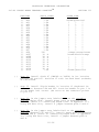
later.) Place a #6 lockwasher on each screw before driving
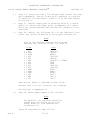
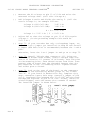
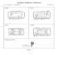
it through the sink into the subchassis. Figure 2—4 shows
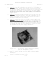
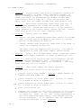
an assembled Sol—lO power supply subchassis.
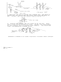
Figure 2—4.
Sol-lO power supply subchassis assembly.
(Rear of subchassis at left.)
*( ) SteP 33. Install bridge rectifier FWB3 on power supply
subchassis.
(Step 33 continued on Page 11-16.)
Rev B
11—15
PROCESSOR TECHNOLOGY CORPORATION
Sol POWER SUPPLY
SECTION II
Position FWB3 (MDA980-l) on power supply subchassis as shown in
drawing on Page X-2. BE SURE NEGATIVE (-) TERMINAL OF
FWB3 is next to transformer. Insert a 6—32 x. ½ binder or
pan head screw from bottom of subchassis, place #6 lockwasher
on screw and secure with 6—32 hex nut.
*( ) Step 34. Connect blue transformer wires to unmarked terminals of FWB3.
*( ) Step 35. Install large (2½”) mounting ring for C9 (54,000
ufd capacitor) on side wall of power supply subchassis as
shown in drawing on Page X-2.
Position ring over the three mounting holes in the side wall
of subchassis so the clamping screw faces the bottom of subchassis and so it will be accessible from the Sol—REG end of
the subchassis. Insert three 6—32 x ½ binder or pan head
screws from outer side of side wall through the mounting
holes. Place #6 lockwasher on each screw and secure with
6-32 hex nut. Figure 2-5 shows an assembled Sol-20 power
supply subchassis.
Figure 2-5.
( )
Sol—20 power supply subchassis assembly.
(Rear of subchassis at left.)
Step 36. Install small (1½”) mounting ring for C8 (18,000
ufd capacitor) as shown in drawing on Page X—2.
(Step 36 continued on Page 11—17.)
Rev B
11—16
PROCESSOR
TECHNOLOGY
CORPORATION
Sol POWER SUPPLY
SECTION II
Position ring over the two mounting holes located between
FWB3 and the Sol-REG so that the clamping screw is positioned
between the transformer and FWB3. Insert two 6-32 x 1/2 binder
or pan head screws from bottom side of chassis through the
mounting holes. Place #6 lockwasher on each screw and secure
with 6-32 hex nut. (Refer to Figure 2-4.)
( ) Step 37.
Route Sol-PC power cable between C8 mounting ring
and the transformer, mount C8 in its mounting ring, and
(See Figure 2-4.)
tiqhten clamping-screw.
( ) Step 38.
Connect white wire of C8 cable to negative (-)
terminal of C8 and green wire to positive (+) terminal of
(This cable was soldered to the Sol-REG when you assemC8.
bled it.) Remove terminal screws, place #1O lockwasher on
each screw, place cable lugs on screws and drive screws
tightly into appropriate terminals.
*( ) Step 39.
Mount C9 in its mounting ring with its "+"
terminal slightly toward C8 and tighten clamping screw.
(See Figure 2-5.)
*( ) S t e p
40.
Prepare R13 (39 ohm 2 watt) for installation on C9.
Solder a #10 lug to each lead of R13. Bend leads of R13 to
fit the terminals of C9.
(R13 should fit on C9 as shown in
Figure 2-5.)
*( ) Step 41.
Connect Sol-20 DC power cable (5 wire) and R13 to
C9. Route cable between C8 and transformer.
Remove terminal screws from C9.
Place lockwasher, terminal
screw, blue lead of Sol-20 DC cable and one R13 lead on one
terminal screw and drive it into the positive (+) terminal
on C9.
Attach lockwasher, white cable lead and other R13
lead to negative (-) terminal on C9 in the same manner.
Tighten both capacitor terminals tightly.
CAUTIONLOOSE CONNECTIONS ON C9 CAN LEAD TO ARCING AND SUBSEQUENT POWER SUPPLY DAMAGE.
*( ) Step 42.
Connect blue pigtail of Sol-20 DC cable to positive
(+) terminal of FWB3.
(This pigtail has a spade lug at its
free end and is connected to the lug you just attached to
the positive terminal of C9.) Connect white pigtail of
Sol-20 DC cable to negative (-) terminal of FWB3.
(This
pigtail has a spade lug at its free end and is connected to
the lug you just attached to the negative terminal of C9.)
PROCESSOR TECHNOLOGY
CORPORATION
SECTION II
Sol POWER SUPPLY
( ) Step 43. Connect green lead from AC receptacle (mounted on
fan closure plate) to power supply subchassis assembly as
(Use the #6 x 1/4 sheet metal
shown in drawing on Page X-2.
screw with which you prethreaded the middle Sol-REG heat
sink mounting hole in Step 29.) Place lug on screw and
drive screw into the middle Sol-REG heat sink mounting hole.
( ) Step 44. Route black transformer leads along side wall of
power supply subchassis out toward the Sol-REG heat sink.
(See Figure 2-4.) Attach one lead to pin 2 of the commoning
block (mounted on fan closure plate) nearest the fan.
Attach
other lead to pin 3 of the other commoning block.
( ) Step 45.
Install cable tie wraps.
( ) Install one wrap around the wires that connect to Sol-REG
pads T1,2,3,X2 and X3 as shown in the Detail A - Wiring
portion of the drawing on Page X-2.
*( ) Install another wrap around the leads from C9 as shown in
Detail B of drawing on Page X-2.
Use them as
Two other wraps are supplied with your kit.
appropriate to make your power supply cabling neater.
( ) Step 46.
Using a #6 x 1/4 sheet metal screw, attach fan closure
plate to power supply subchassis as shown in Drawing No. X-2.
( ) Step 47.
Push on-off switch in and out to determine the OFF
position (switch mechanically out). With switch in OFF
Then plug
position, connect AC power cord to AC receptacle.
power cord into 110 V ac outlet.
( ) Step 48.
Test power supply for proper operation.
Make sure on-off switch is in OFF position.
Install fuse in fuse holder.
REMOVE FUSE WITH POWER ON.
CAUTION:
NEVER INSTALL OR
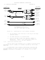
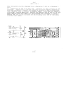
Check connector on Sol-PC power cable (4 wire) to insure
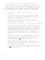
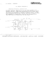
it is wired as shown in Figure 2-6.
Check connector on Sol-20 power cable (5 wire) to insure
it is wired as shown in Figure 2-7.
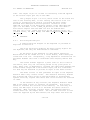
Turn on-off switch ON.
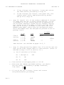
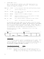
Measure the voltages at the Sol-PC connector at the points
indicated in Figure 2-6. The voltages must be as given
in Figure 2-6. NOTE:
Do not take voltage measurements at
any other points in the power supply, even through they may
It is important that the indicator
be more accessible.
voltages be available at the connector.
II-18
Rev B
PROCESSOR
TECHNOLOGY
CORPORATION
Sol POWER SUPPLY
SECTION II
*( ) Measure the voltages at the Sol-20 connector at the
points indicated in Figure 2-7. The voltages must be
within the ranges given in Figure 2-7.
(See preceding
NOTE.)
( ) If the power supply fails any of the preceding tests,
locate and correct the cause before proceeding.
If the power supply is operating correctly, turn on-off
switch OFF, disconnect power cord, set power supply to one
side and go on to Section III.
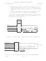
---------
Red
-----
White/Yellow
Green
White
1----- ;
+12 V dc
-----12
V
dc
(+ .6 v)
I
<
(+.6V)
+5 V dc
(Ground) ----,
q (5 .25 v)
Figure 2-6.
Sol-PC power connector and voltage measurements.
Yellow/White
Red/White
Blue
White (Gnd 1)
White
(Gnd
2)
----L
Figure 2-7.
Rev B
+7.5 to 11 V dc
1
Sol-20 power connector and voltage measurements.
II-19
III
Sol-PC ASSEMBLY and TEST
3.1
Parts and Components . . . . . . . . . . . .
III-1
3.2
Assembly Tips
. . . . . . . . . . . . . . .
III-1
3.3
Assembly Precautions . . . . . . . . . . . .
III-6
3.3.1
3.3.2
Handling MOS Integrated Circuits . .
Soldering . . . . . . . . . . . . . .
III-6
III-6
3.3.3
3.3.4
Power Connection (J10)
Installing and Removing
Circuits . . . . . . .
Installing and Removing
Module . . . . . . . .
Use of Clip Leads . . .
.
III-6
.
III-6
.
.
III-6
III-7
. .
III-7
3.3.5
3.3.6
. . . . . .
Integrated
. . . . . .
Personalit
. . . . . .
. . . . . .
3.4
Required Tools, Equipment and Materials
3.5
Orientation (Sol-PCB)
. . . . . . . . . . .
III-7
3.6
Sol-PC Assembly-Test Procedure . . . . . . .
III-7
3.6.1
3.6.2
3.6.3
3.6.4
III-8
III-9
III-9
III-40
Circuit Board Check . . . . . .
Personality Module Assembly . .
Sol-PCb Assembly and Test . . .
Modification for 625 Line Video
.
.
.
.
.
.
.
.
.
.
.
.
PROCESSOR
TECHNOLOGY
Sol-PC SINGLE BOARD TERMINAL COMPUTERTM
3.1
CORPORATION
SECTION III
PARTS AND COMPONENTS
Check all parts and components against the "Parts List" on
Pages III-2 through III-4 (Table 3-l). If you have difficulty in
identifying any parts by sight, refer to Figure 3-l on Page 111-5.
3.2
ASSEMBLY TIPS
1.
Scan Sections III and IV in their entirety before you
start to assemble your Sol-PC kit.
2.
In assembling your Sol-PC, you will be following an integrated assembly-test procedure. Such a procedure is designed to
progressively insure that individual circuits and sections in the
Sol-PC are operating correctly. IT IS IMPORTANT THAT YOU FOLLOW THE
STEP-BY-STEP INSTRUCTIONS IN THE ORDER GIVEN.
3.
Assembly steps and component installations are preceded
by a set of parentheses. Check off each installation and step as
you complete them. This will minimize the chances of omitting a
step or component.
4.
When installing components, make use of the assembly aids
that are incorporated on the circuit boards and the assembly drawings.
(These aids are designed to assist you in correctly installing the
components.)
a. The circuit reference (R3, C10 and U20, for example)
for each component is silk screened on the PC boards
near the location of its installation.
b.
Both the circuit reference and value or nomenclature
(1.5K and 74H00,
for example) for each component are
included on the assembly drawings near the location
of its installation.
5 . To simplify reading resistor values after installation,
install resistors so that the color codes or imprints read from left
to right and top to bottom as appropriate (boards oriented as defined
in Paragraph 3.5 on Page 111-7).
6. Unless specified otherwise, install components, especially
disc capacitors, as close as possible to the boards.
7 . Should you encounter any problem during assembly, call
on us for help if needed.
III-1
PROCESSOR
TECHNOLOGY
CORPORATION
Sol-PC SINGLE BOARD TERMINAL COMPUTERTM
Table 3-1.
INTEGRATED
SECTION III
Sol-PC Parts List.
CIRCUITS
1
AM0026 or DMO026 (U104)
1
4N26 (U39)
1
5
8T94 (U58)
8T97 (U67,68,77,80,81)
2
1
2
1
1
1458CP or 1558CP (U56,108)
1489A (U38)
TMS6O11NC (U51,69)
MCM6574 or MCM6575 (U25)
4001 (U102)
2
1
1
4013 (U100,113)
4019 (U111)
4023 (u98)
1
1
4024 (U86)
4027 (U101)
3
1
4029 (U1,11,84)
4030 (U99)
2
2
1
1
3
2
4
4046 (U85,110)
4049 (U88,109)
4520 (U112)
74H00 (U91)
74LS00 (U44,48,55)
74LS02 or 9LS02 (U53,60)
74LS04 (U24,45,49,54)
TRANSISTORS
74S04 (U92)
7406 (U57,87)
74LS10 (U47,61)
74LS20 (U23,59,83)
74LS86 (U74)
74LS109 (U43,52,63,64,70,
72,73,75)
74LS136 (U22)
4
7
1
1
16
1
74LS138 (U34,35,36)
74LS157 (U12,30,32)
74LS163 or 25LS163
(U28,31,33,40)
74166 (U41)
74173 (U95,96)
74175 (U97)
74LS175 or 25LS175
(U2,13,26,27,42,76,90,93,106
74LS253 (U65,66,78,79)
74LS367 (U29,37,50,71,89,
94,107)
8080, 8080A or 9080A (U105)
8836 or 8T380 (U46)
91L02APC or 2102L1PC
(U3 10, U14 - 21)
93L16 (U62)
DIODES
2 2N2222 (Q4 & Q5)
2 2N2907 or 2N3460 (Q1 & Q2)
1 2N4360 (Q3)
9 1N4148 or 1N914 (D1,D3 - 10)
1 1N5231B Zener Diode (D11)
4 1N4001 (D2,12,13,14)
CRYSTAL
1 14.318 MHz in HC-18/U Case
(XTAL)
RELAYS
2 DIP Reed, Sigma 19l-TE1A15S
(K1 & K2)
III-2
PROCESSOR TECHNOLOGY CORPORATION
TM
501-PC SINGLE BOARD TERMINAL COMPUTER
(Continued)
SECTION III
Table 3-1. Sd—PC Parts List (Continued).
RESISTORS
2
6.8
2 47
1 75
1 100
3 100
1 200
13 330
1 330
3 470
2 470
9 680
63
1.5K
1
3.3K
6
5.6K
32 10 K
1 15 K
2 39 K
1 47 K
3 50 K
4 100 K
2 150 K
2
1 M
1
2.2M
2
3.3M
ohm,
ohm,
ohm,
ohm,
ohm,
ohm,
ohm,
ohm,
ohm,
ohm,
ohm,
ohm,
ohm,
ohm,
ohm,
ohm,
ohm,
ohm,
ohm,
ohm,
ohm,
ohm,
ohm,
ohm,
½ watt, 5%
¼ watt, 5%
¼ watt, 5%
¼ watt, 5%
½ watt, 5%
¼ watt, 5%
¼ watt, 5%
½ watt, 5%
¼ watt, 5%
½ watt, 5%
¼ watt, 5%
¼ watt, 5%
¼ watt, 5%
¼ watt, 5%
¼ watt, 5%
¼ watt, 5%
¼ watt, 5%
¼ watt, 5%
Potentiometer
¼ watt, 5%
¼ watt, 5%
¼ watt, 5%
¼ watt, 5%
¼ watt, 5%
CAPACI TORS
1
10
1 330
1 470
3 680
6
2
2
37
12
1
1
1
.001
.001
.01
.047
.1
.1
.68
1
5
15
1
100
pfd,
pfd,
pfd,
pfd,
disc
disc
disc
monolythic or disc
ceramic (labeled
681 and usually
blue)
ufd,
ufd,
ufd,
ufd,
Ufd,
ufd,
ufd,
ufd, tantalum dipped
(usually orange or
red)
ufd, tantalum dipped
(usually orange or
red)
ufd, aluminum
electrolytic
CONNECTORS
1
1
2
1
2
2
1
1
1
Rev A
25-pin Female, AMP206584—2 (J1)
25—pin Male, AMP206604—1 (J2)
20—pin Header, 3M3492-2002 (J3 & J4)
30-pin Right Angle Edge Connector, VIKING 3KH15/1JKC15 (J5)
Miniature Phone Jack (J6 & J7)
Subminiature Phone Jack (J8 & J9)
7-pin Male Locking Molex Connector (J1O)
100—pin Edge Connector, TI H322150-0306A (J11)
Molex-type DC Power Cable, mates with JlO (prefabricated)
III-3
PROCESSOR TECHNOLOGY CORPORATION
Sol-PC SINGLE BOARD TERMINAL COMPUTERTM
SECTION III
Table 3-1. Sal—PC Parts List (Continued).
MISCELLANEOUS
1 Sol—PCB Circuit Board
length of #24 bare wire
2 8-pin DIP Socket
29 14-pin DIP Socket
74 16-pin DIP Socket
1 24-pin DIP Socket
3 40-pin DIP Socket
16 Augat Pins on Carrier
2 DIP Switch, 6 position (Sl & S4)
2 DIP Switch, 8 position (S2 & S3)
1 4-foot Length 72-ohm Coaxial Cable
1 Tie Wrap for Coaxial Cable
2 Mounting Bracket, Sol-1040
2 Card Guide, SAEl250F
10 #4 Lockwasher, internal tooth
2 #4 Insulating Washer
4 4-40 x ¼ Binder Head Screw
6 4-40 x 7/16 Binder Head Screw
2 4-40 x 5/8 Binder Head Screw
10 4-40 Hex Nut
1 Length Solder
1 Manual
1 Personality Module Kit (See Section IV for contents.)
III-4
PROCESSOR
TECHNOLOGY CORPORATION
TM
Sol-PC SINGLE BOARD TERMINAL COMPUTER
3.3
ASSEMBLY
3.3.1
Handling MOS Integrated Circuits
SECTION III
PRECAUTIONS
Many of the IC's used in the Sol-PC are MOS devices. They can
be damaged by static electricity discharge. Always handle MOS IC's
so that no discharqe will flow throuqh the IC. Also, avoid unnecessary handling and wear cotton--rather than synthetic--clothing when
you do handle these IC's.
3.3.2
Soldering
1.
**IMPORTANT**
Use a fine tip, low-wattage
iron, 25 watts maximum.
DO NOT use excessive amounts of solder.
2.
and as quickly as possible.
Use only 60-40 rosin-core solder.
3.
solder or externally applied fluxes.
DO solder neatly
NEVER use acid-core
To prevent solder bridges, position iron tip so that it
4.
does p not m touch
adjacent
pins and/or
- traces
- - - simultaneously.
- 5.
DO NOT press tip of iron on pad or trace.
To do so can
cause the pad or trace to "lift" off the board and permanently damage
the board.
6.
The Sol-PC uses circuit boards with plated-through holes.
Solder flow through to the component (front) side of the board can
produce solder bridges.
Check for -such- bridqes
after
- you -install
each component.
7.
The Sol-PC circuit boards have integral solder masks (a
lacquer coating) that shield selected areas on the boards.
This mask
minimizes the chances of creating solder bridges during assembly. DO,
however, check all solder joints for possible bridges.
Additional pointers on soldering are provided in Appendix
8.
IV of this manual.
Power Connection (J1O)
NEVER connect the DC power cable to the Sol-PC when power
supply is energized. To do so can damage the Sol-PC.
3.3.3
Installing and Removing Integrated Circuits
NEVER install or remove integrated circuits when power is
applied to the Sol-PC. To do so can damage the IC.
3.3.4
3.3.5
Installing and Removing Personality Module
NEVER install or remove the plug-in personality module when
power is applied to the Sol-PC. To do so can damage the module.
Rev A
III-6
PROCESSOR
TECHNOLOGY
Sol-PC SINGLE BOARD TERMINAL
COMPUTERTM
3.3.6
CORPORATION
SECTION III
Use of Clip Leads
TARE CARE when using a clip lead to establish a ground connection when testing the Sol-PCB circuit board. Make sure that the
clip makes contact only with the ground bus on the perimeter of the
board.
3.4
REQUIRED TOOLS, EQUIPMENT AND MATERIALS
The following tools, equipment and materials are recommended
for assembling and testing the Sol-PC:
3.5
1.
Needle nose pliers
2.
Diagonal
3.
Screwdriver
4.
Sharp knife
5.
Controlled heat soldering iron, 25 watt
6.
60-40 rosin-core solder (supplied)
7.
Small amount of #24 solid wire
8.
Volt-ohm
9.
Video monitor or monochrome TV converted for video input.
cutters
meter
10.
IC test clip (optional)
11.
Oscilloscope
ORIENTATION
(optional)
(Sol-PCB)
Location J5 (personality plug-in module connector) will be
located in the upper right-hand area of the circuit board when location J1O (power connector) is positioned at the bottom of the board.
In this position the component (front) side of the board is facing
up and all IC legends (U1 through U10, U22 through U24, etc.) will
Subsequent position references related to
read from left to right.
the Sol-PCB assume this orientation.
3.6
Sol-PC
ASSEMBLY-TEST
PROCEDURE
The Sol-PC is assembled and tested in sections and/or circuits. You will first test the Sol-PCB circuit board for shorts
(solder bridges) between the power buses and ground. After assembling
III-7
PROCESSOR
TECHNOLOGY CORPORATION
Sol-PC SINGLE BOARD TERMINAL COMPUTERTM
SECTION III
the personality module (see Section IV), the clock and display control
circuits are assembled. The bus, CPU, decoder and memory circuits are
then assembled, followed by the parallel and serial input/output (I/O)
and audio cassette I/O sections.
CAUTION
THE Sol-PC USES MANY MOS INTEGRATED
THEY CAN BE DAMAGED BY
CIRCUITS.
STATIC ELECTRICITY DISCHARGE. HANDLE
THESE IC's SO THAT NO DISCHARGE FLOWS
AVOID UNNECESSARY
THROUGH THE IC.
HANDLING AND WEAR COTTON, RATHER THAN
SYNTHETIC, CLOTHING WHEN YOU DO HANDLE
MOS IC's.
(STATIC CHARGE PROBLEMS ARE
MUCH WORSE IN LOW HUMIDITY CONDITIONS.)
3.6.1
Circuit Board Check
( ) Visually check Sol-PCB board for solder bridges (shorts)
between traces, broken traces and similar defects.
( ) Check board to insure that the +5-volt-bus, +12 volt-bus
and -12-volt bus are not shorted to each other or to
ground.
Using an ohmmeter, on "OHMS X 1K" or "OHMS X 10K"
scale, make the following measurements (refer to Sol-PC
Assembly Drawing X-3).
( ) +5-volt Bus Test.
Measure between positive and negative mounting pads for C58.
There should be no
continuity. (Meter reads close to "infinity" ohms.)
( ) +12-volt Bus Test.
Measure between positive and negative mounting pads for C59.
There should be no
continuity.
( ) -12-volt Bus Test.
Measure between positive and negative mounting pads for C60.
There should be no
continuity.
( ) 5/12/(-12) Volt Bus Test.
Measure between positive
mounting pads for C58 and C59, between positive pad
for C58 and negative pad for C60, and between positive pad for C59 and negative pad for C60. You should
measure no continuity in any of these measurements.
If visual inspection reveals any defects, or you measure
continuity in any of the preceding tests, return the
board to Processor Technology for replacement.
If the
board is not defective, proceed to next paragraph.
Rev A
III-8
PROCESSOR
TECHNOLOGY
CORPORATION
Sol-PC SINGLE BOARD TERMINAL COMPUTERTM
3.6.2
Personality
Module
SECTION III
Assembly
Since the personality module is required for testing the SolPC in the later stages of its assembly,
we suggest that you assemble
the personality module first.
In so doing, your Sol-PC assembly will
proceed uninterrupted.
Assembly instructions for the personality
module are provided in Section IV of this manual.
If you wish to wait to assemble the personality module until
it is needed, go on to Paragraph 3.6.3.
3.6.3
Sol-PCB Assembly and Test
Refer to Sol-PC assembly drawing X-3.
Install DIP sockets.
Install each socket in the in( ) Step 1.
dicated location with its end notch oriented as shown on the
circuit board and assembly drawinq.
Take care not to create
solder bridges between the pins and/or traces.
(Refer to
footnotes at end of this step before installing U105.)
INSTALLATION TIP
Insert socket pins into mounting pads of
appropriate location.
On solder (back)
side of board, bend pins at opposite corners of socket (e.g., pins 1 and 9 on a
16-pin socket) outward until they are at
a 45 angle to the board surface.
This
secures the socket until it is soldered.
Repeat this procedure with each socket
until all are secured to the board.
Then
solder the unbent pins on all sockets.
Now straighten the bent pins to their
original position and solder.
LOCATION
(
(
(
(
(
(
(
(
(
(
(
(
(
(
Rev B
)
)
)
)
)
)
)
)
)
)
)
)
)
)
TYPE SOCKET
16 pin
U1 through 21
14 pin
U22 through 24
U25
24 pin
U26 through 37
16 pin
U38
14 pin
U39
None
U40 through 43
16 pin
U44 through 49
14 pin
U50
16 pin
U51
40 pin
U52
16 pin
U53 through 55
14 pin
U56
8 pin
U57 through 61
14 pin
(Continued on Page III-10.)
III-9
PROCESSOR TECHNOLOGY CORPORATION
Sol-PC SINGLE BOARD TERMINAL COMPUTERTM
LOCATION
(
(
(
(
(
(
(
(
(
(
(
(
(
(
(
(
(
(
(
(
(
(
)
)
)
)
)
)
)
)
)
)
)
)
)
)
)
)
)
)
)
)
)
)
SECTION III
TYPE SOCKET
U62 through 68
U69
U70 through 73
U74
U75 through 81
U82#
U83
U84,85
U86,87
U88 through 90
U91,92
U93 through 97
U98 through 100
UlOl
U102
U103*
U104
U105*
U106,107
UlOB
U109 through 112
U113
16 pin
40 pin
16 pin
14 pin
16 pin
None#
14 pin
16 pin
14 pin
16 pin
14 pin
16 pin
14 pin
16 pin
14 pin
None#
None
40 pin
16 pin
8 pin
16 pin
14 pin
#Spare locations, not used.
*Note that U105 notch is positioned at the top.
( )
Step 2. Install the following capacitors in the indicated
locations. Take care to observe the proper value, type and
orientation, if applicable, for each installation. Bend
leads outward on solder (back) side oiI board, solder and
trim.
NOTE
Disc capacitor leads are usually coated
with wax during the manufacturing process. After inserting leads through
mounting holes, remove capacitor and
clear the holes of any wax. Reinsert
and install.
LOCATION
(
(
(
(
(
(
(
(
)
)
)
)
)
)
)
)
Cl
C2
C3
C4
C5
C6
C7
C8
VALUE (ufd)
.047
.047
.047
.047
.047
.047
.047
.047
TYPE
Disc
”
”
”
”
”
”
”
111—10
ORIENTATION
None
”
”
”
”
”
”
”
PROCESSOR TECHISIOLOGY CORPORATION
Sol-PC SINGLE BOARD TERMINAL COMPUTERTM
LOCATION
(
(
(
(
(
(
VALUE (ufd)
.047
.047
.047
.047
TYPE
ORIENTATION
)
)
)
)
)
)
C10
C11
C13
C14
C15
C16
( )
Step 3. Check for +5-volt bus to ground shorts. Using an
ohmmeter, measure between positive and negative mounting
pads for C58. There should be no continuity. If there is,
find and correct the problem before proceeding to Step 4.
15
.047
Disc
“
“
“
Tantalum
Disc
SECTION III
None
“
“
“
“+” lead bottom
None
( ) Step 4. Install the following capacitors in the indicated
locations. Take care to observe the proper value1 type and
orientation, if applicable, for each installation. Bend
leads outward on solder (back) side of board, solder and
trim. (refer to NOTE in Step 2.)
LOCATION
(
(
(
(
(
(
(
(
(
(
(
(
(
(
(
(
(
)
)
)
)
)
)
)
)
)
)
)
)
)
)
)
)
)
C19
C20
C21
C24
C25
C26
C33
C38
C40
C41
C42
C45
C56
C58
C59
C60
C65
VALUE (ufd)
.047
.047
.047
.047
.047
.047
.047
.047
15
.047
.047
.047
.047
15
15
15
.047
TYPE
Disc
“
“
“
“
“
“
“
Tantalum
Disc
“
“
“
Tantalum
Tantalum
Tantalum
Disc None
ORIENTATION
None
“
“
“
“
“
“
“
+” lead
None
“
“
“
“+” lead
“+” lead
“+” lead
bottom
top
top
top
( ) Step 5. Check for +5-volt bus to ground shorts. Using an
ohmmeter, measure between the positive and negative leads of
C58. You should measure at least 100 ohms. Less than 100
ohms indicates a short. If required, find and correct the
problem before proceeding to Step 6. NOTE: In this and
subsequent resistance measurements, any value greater than
the minimum may normally occur, even much higher, unless
otherwise indicated.
( ) Step 6. Install the following capacitors in the indicated
locations. Take care to observe the proper value and type
for each installation. Bend leads outward on solder (back)
side of board, solder and trim. (Refer to NOTE in Step 2.)
(Step 6 continued on Page 111—12.)
Rev A
111—11
PROCESSOR TECHNOLOGY CORPORATION
Sol-PC SINGLE BOARD TERMINAL COMPUTERTM
LOCATION
(
(
(
(
(
(
(
(
(
)
)
)
)
)
)
)
)
)
VALUE (ufd)
C9
C12
C17
C18
C22
C23
C27
C28
C46
SECTION III
TYPE
.047
.047
.047
.047
.047
.047
.047
.047
.047
Disc
“
“
“
“
“
“
“
“
ORIENTATION
None
“
“
“
“
“
“
“
“
( )
Step 7. Check for +5-volt bus to ground shorts. Using an
ohmmeter, measure between the positive and negative leads of
C58. You should measure some resistance. Zero resistance
indicates a short. If required, find and correct the problem
before proceeding to Step 8.
( )
Step 8. Install diodes D8 (1N4148 or 1N914), D11 (1N5231B)
and D12 (1N4001) in their locations (in the area below U90
through U92). Position D8 with its dark band (cathode) to
the right, Dll with its band at the bottom, and D12 with
its band at the top.
NOTE
The leads of D12 and its mounting holes
are a snug fit. Take care when installing this diode.
( )
Step 9. Install the following resistors in the indicated
locations. Bend leads to fit distance between mounting
holes, insert leads, pull down snug to board, solder and
trim.
LOCATION
VALUE ohms
COLOR CODE
(
(
(
(
(
(
(
(
(
(
)
)
)
)
)
)
)
)
)
)
( )
R104
R105
R106
R130
R131
R132
R133
R134
R135 & 136
R137 & 138
10 K
1.5K
1.5K
100, ½ watt
100, ½ watt
100, ½ watt
330
330
10 K
47
brown-black-orange
brown-green-red
“
“
“
brown—black—brown
“
“
“
“
“
“
orange-orange-brown
“
“
“
brown-black-orange
yellow—violet—black
Step 10. Install the following capacitors in the indicated
locations. Take care to observe the proper value and type
for each installation. Bend leads outward on solder (back)
side of board, solder and trim. (Refer to NOTE in Step 2.)
111—12
PROCESSOR TECHNOLOGY CORPORATION
Sol-PC SINGLE BOARD TERMINAL COMPUTERTM
LOCATION
(
(
(
(
(
(
(
)
)
)
)
)
)
)
VALUE
C39
C43
C44
C61
C62
C63
C64
SECTION III
TYPE
.1
ufd
pfd
pfd
.001 ufd
.68 ufd
.1
ufd
10
pfd
Disc
Monolythic or Disc
Monolythic or Disc
Disc
Monolythic
Disc
Disc
680
680
( )
Step 11. Install 14.318 MHz crystal in its location just
above C61. Insert leads and pull down until the case is
1/16" above the front surface of the board. Solder quickly
and trim.
( )
Step 12. Install male Molex connector in location
J10. Position conncctor so the locking clip is facing
the crystal (XTAL), insert shorter pins in mounting
holes and solder.
( )
Step 13. In the jumper area labeled CLK on the assembly
drawing (between U90 and U91), install Augat pins in mounting holes A,B,C,D and E. (Refer to "Installing Augat Pins"
in Appendix IV.) Using #24 bare wire, install a jumper between the A and B pins and another jumper between the D and
E pins.
( )
Step 14. Install the following IC’s in the indicated locations. Pay careful attention to the proper orientation. DO
NOT SUBSTITUTE FOR ANY OF THESE IC’s.
NOTE
Dots on the assembly drawing and PC board
indicate the location of pin 1 of each IC.
IC NO.
(
(
(
(
(
)
)
)
)
)
U77
U90
U91
U92
U104*
TYPE
8T97
74L5175 or 25L5175
74H00
74S04
AM0026 or DM0026*
*Solder this IC in its location.
See "Loading DIP Devices" in
Appendix IV.
( )
Step 15. Connect power to power connector J10. Power and
interconnection requirements are as follows:
(Step 15 continued on Page 111-14.)
111—13
PROCESSOR TECHNOLOGY CORPORATION
Sol-PC SINGLE BOARD TERMINAL COMPUTERTM
SECTION III
CAUTION 1
NEVER CONNECT POWER CABLE TO J10 WITH
POWER SUPPLY ENERGIZED.
CAUTION 2
MAKE SURE POWER CABLE CONNECTOR MATES
EXACTLY WITH J10; THAT IS, PIN 1 TO
PIN 1, PIN 2 TO PIN 2, ETC. ANY OTHER
MATING RELATIONSHIP WILL “BLOW” THE
IC’ s.
1 2 3 4 5 6 7
(J10, Top View)
J10 PIN NO.
1
2and6
3and5
4
7
POWER
Ground
+5Vdc+5%,
2 Amax
-l2Vdc+5%, 300mAmax
+l2Vdc+5%, l00mAmax
Ground
NOTE
Though not labeled on the connector, J10
pins are designated 1 through 7, reading
from left to right.
( )
Step 16. Check clock circuits. If you have an oscilloscope,
use part A of this step. If you do not, use part B.
A.
( )
Oscilloscope Check
Using an oscilloscope, check for the waveforms given in
Figure 3-2 on Page 111-15 at the indicated observation
points and in the order given. The waveforms shown in
Figure 3—2 approximate actual waveforms. If any waveforms
are incorrect, determine and correct the cause before proceeding with assembly.
NOTE
Irregularities up to 1 volt are acceptable on positive portions of waveforms.
Negative portions, however, should be
relatively flat.
B.
Volt-ohm Meter Check
( )
Using the test probe shown in Figure 3-3 on Page 111-16,
set meter to DC volts and make the following measurements:
(Volt-ohm Meter Check continued on Page 111—16.)
111—14
PROCESSOR TECHNOLOGY CORPORATION
Sol-PC SINGLE BOARD TERMINAL COMPUTERTM
CHECK POINT
SIGNAL
( )
U77,
Pin 7
Oscillator
Output
( )
U91,
Pin 6
Clock
Divider
Output
SECTION III
WAVEFORM
14.3 MHz square wave. (This is not a
perfect square wave. It in fact more
resembles a poor sine wave.)
4V
70
ns
430 ns
Gnd
4V
( )
U91,
Pin 11
Clock
Divider
Output
270 ns
230 ns
Gnd
12V
( )
U104,
Pin 7
CPU
Clock
01
70
ns
430 ns
Gnd
12V
( )
U104,
Pin5
CPU
Clock
02
270 ns
230 ns
Gnd
Figure 3—2. Clock circuit waveforms.
111—15
PROCESSOR TECHNOLOGY CORPORATION
Sol-PC SINGLE BOARD TERMINAL COMPUTERTM
SECTION III
Figure 3-3. Test probe for Steps 16B and 25B.
NOTE 1
The probe shown in Figure 3-3 can be
made using parts supplied with your
Sol-PC kit. Since these parts will
be used later in the Sal-PC assembly,
DO NOT shorten the leads or otherwise
alter the components. Assemble the
probe using tack soldering technique.
NOTE 2
Make sure you have a good ground connection between the meter, probe and
Sol—PCB.
( )
At pin 7 of U77 you should measure 1.5 V dc or
higher. (A significantly lower reading indicates
a faulty oscillator circuit.)
( )
At pin 6 of U91 you should measure 0.25 V dc or
higher. (A significantly lower reading indicates
a faulty clock divider, U90.)
( )
At pin 11 of U91 you should measure 1.25 V dc or
higher. (A significantly lower reading indicates
a faulty clock divider, U90.)
( )
At pin 5 of U104 you should measure 4 V dc or higher.
(A significantly lower reading indicates a problem
with U104.)
( )
At pin 7 of U104 you should measure 8 V dc or higher.
(A significantly lower reading indicates a problem
with U104.)
( )
If any voltages are incorrect, correct the problem
before proceeding; if correct, turn off the power
supply and disconnect the power cable.
Rev B
111-16
PROCESSOR TECHJWLOGY CORPORATION
Sol-PC SINGLE BOARD TERMINAL COMPUTERTM
( )
Step 17. Install the following resistors in the indicated
locations. Bend leads to fit distance between mounting holes,
insert leads, pull down snug to board, solder and trim.
LOCATION
(
(
(
(
(
(
(
(
(
(
(
(
(
(
(
(
(
(
(
(
(
(
(
(
(
(
(
(
(
(
(
(
(
(
(
(
(
(
(
(
(
(
(
(
(
)
)
)
)
)
)
)
)
)
)
)
)
)
)
)
)
)
)
)
)
)
)
)
)
)
)
)
)
)
)
)
)
)
)
)
)
)
)
)
)
)
)
)
)
)
SECTION III
R1
R2
R3
R4
R5
R6
R7
R8
R9
R10
R11
R16
R17
R19
R30
R80*
R81
R82
R83
R84
R85
R86
R87
R88
R89
R90
R96
R97
R98
R99
RlOO
RlOl
R102
R103
R120
R121
R122
R123
R124
R125
R126
R127
R128
R129
VRl & VR2
VALUE (ohms)
1.5K
1.5K
1.5K
1.5K
1.5K
1.5K
1.5K
1.5K
1.5K
1.5K
1.5K
1.5K
1.5K
1.5K
1.5K
330, ½ watt
75
200
1.5K
3.3M
1.5K
1.5K
330
680
1.5K
1.5K
1.5K
1.5K
10 K
1.5K
10 K
1.5K
3.3M
1.5K
100 K
10 K
10 K
39 K
1.5K
1.5K
39 K
10 K
3.3K
10 K
50 K
COLOR CODE
brown-green-red
”
”
”
”
”
”
”
”
”
”
”
”
”
”
”
”
”
”
”
”
”
”
”
”
”
”
”
”
”
”
”
”
”
”
”
”
”
”
”
”
”
”
orange-orange-brown
violet—green-black
red-black-brown
brown-green-red
orange—orange—green
brown-green-red
”
”
”
orange-orange-brown
blue-gray-brown
brown-green-red
”
”
“
”
”
”
”
”
”
brown-black-orange
brown-green-red
brown-black-orange
brown-green-red
orange-orange-green
brown-green—red
brown-black-yellow
brown-black-orange
”
”
”
orange-white-orange
brown-green—red
”
”
”
orange-white-orange
brown-b1ack-orange
orange—orange-red
brown-black-orange
Potentiometer
*The leads of R80 and its mounting holes form a snug
fit. Take care when installing this resistor.
Rev A
111—17
PROCESSOR TECHNOLOGY CORPORATION
Sol-PC SINGLE BOARD TERMINAL COMPUTERTM
SECTION III
( ) Step 18. Install the following capacitors in the indicated
locations. Take care to observe the proper value and type
for each installation. Bend leads outward on solder (back)
side of board, solder and trim. (Refer to NOTE in Step 2.)
CAUTION
REFER TO FOOTNOTE AT END OF THIS STEP BEFORE
INSTALLING C31.
LOCATION
(
(
(
(
(
(
(
(
(
(
(
)
)
)
)
)
)
)
)
)
)
)
C31*
C32
C34
C35
C36
C37
C52
C53
C54
C55
C57
*Install
VALUE
TYPE
100
ufd
Aluminum Electrolytic
ufd
Disc
680
pfd
Monolythic or Disc
.1
ufd
Mylar Tubular
.1
ufd
Disc
.1
ufd
Disc
.001 ufd
Mylar Tubular
.01 ufd
Mylar Tubular
.001 ufd
Disc
.001 ufd
Disc
.1
ufd
Disc
with “+” lead at the top.
.1
C31
( )
Step 19. Install Q2 (2N2907 or 2N3460) in its location below
and to the right of U88. The emitter lead (closest to tab on
can) is oriented toward the left of the board and the base is
oriented toward the bottom. Push straight down on transistor
until it is stopped by the leads. Solder and trim.
( )
Step 20. Install diodes D9 and DlO (1N4148 or 1N914) in
their locations below U88. Position D9 with its dark band
(cathode) to the left and DlO with its band to the right.
( )
Step 21. Install coaxial cable, composite video output. (See
Figure 3-4 for details on how to prepare cable.)
( )
Strip away about 1¼” of the outer insulation to expose
shield. Unbraid shield, gather and twist into a single
lead. Then strip away the inner conductor insulation,
leaving about ¼” at the shield end.
CAUTION
WHEN PREPARING AND INSTALLING SHIELD, BE
SURE BITS OF BRAID DO NOT FALL ONTO BOARD.
SUCH DEBRIS CAN CREATE HARD-TO-FIND SHORT
CIRCUITS.
( )
Insert inner conductor in mounting hole P1 (left side of
board), solder and trim.
111—18
PROCESSOR
TECHNOLOGY CORPORATION
Sol-PC SINGLE BOARD TERMINAL COMPUTERTM
SECTION III
Outer
Inner Conduct0
Figure 3-4.
Insulation
Coaxial cable preparation.
( ) Insert twisted shield in mounting hole P2, solder and
trim.
Using the two large holes to the right of VR1 and
VR2, tie cable to board with tie wrap (see CAUTION below).
CAUTION
AFTER INSTALLATION, FINE BITS OF THE BRAID
FROM THE SHIELD MAY WORK LOOSE AND FALL
ONTO THE BOARD AND CREATE HARD-TO-FIND
SHORT CIRCUITS. TO PREVENT THIS, COAT ALL
EXPOSED BRAID WITH AN ADHESIVE AFTER SOLDERING AND TIEING. USE AN ADHESIVE SUCH
AS SILICONE, CONTACT CEMENT OR FINGERNAIL
POLISH. DO NOT
- USE
- WATER BASE ADHESIVES.
( )
S1 on
Step 22.
Install 6-position DIP switch in location
left end of board.
Position Switch No. 1 at the bottom.
( )
Step
23.
Install
20-pin
header
in
location
J4
Position header so
sion connector) between U28 and U29.
(An arrow on the conpin 1 is in the lower right corner.
nector points to pin 1.)
Install the following IC's in the indicated locaPay careful attention to the proper orientation.
NOTE
Dots on the assembly drawing and PC
board indicate the location of pin 1
of each IC.
IC NO.
TYPE
- 74LS163
74LS163
74LS163
74LS163
74LS109
74LS10
74LS04
or
or
or
or
25LS163
25LS163
25LS163
25LS163
(Step 24 continued on Page 111-20.)
III-19
(video
PROCESSOR
TECHNOLOGY CORPORATION
Sol-PC SINGLE BOARD TERMINAL COMPUTERTM
IC NO.
(
(
(
(
(
(
(
(
)
)
)
)
)
)
)
)
SECTION III
TYPE
U59
U60
U62
U74
U75
U87
U88*
U102*
74LS20
74LS02 or 9LS02
93L16
74LS86
74LS109
7406
4049*
4001*
*MOS device.
Refer to CAUTION on Page 111-8.
( ) Step 25. Apply power to Sol-PC and check display section
timing chain operation. If you have an oscilloscope, use
part A of this step. If you do not, use part B.
A.
Oscilloscope
Check
( ) Using an oscilloscope, check for the waveforms given
in Figure 3-5 at the indicated observation points and
in the order given. The waveforms shown in Figure
3-5 approximate actual waveforms. If any waveforms
are incorrect, determine and correct the cause before
proceeding with assembly.
NOTE
Irregularities up to 1 volt are acceptable on positive portions of waveforms.
Negative portions, however, should be
relatively flat.
B.
Volt-ohm Meter Check
( ) Using the test probe made in Step 16B, measure the
voltage at pin 12 of U28. You should measure approximately 1 V dc. If you get a significantly lower
reading, find and correct the cause before you proceed with assembly.
( ) Turn off power supply and disconnect power connector.
( ) Step 26. Check synchronization circuits.
( ) Set all S1 switches to OFF.
( ) Connect Sol-PC video output cable to video monitor.
SEE CAUTION ON PAGE III-22 BEFORE CONNECTING MONITOR.
(Step 26 continued on Page 111-22.)
III-20
PROCESSOR
TECHNOLOGY
CORPORATION
Sol-PC SINGLE BOARD TERMINAL COMPUTERTM
SECTION III
WAVEFORM
CHECK POINT
4 V
ti*O+ 250 ns -1
( ) U28, Pin 12
Gnd
( ) U47, Pin 8
(
) U59,
Pin8
ns
+i
<
600
-9f-
550 ns
64 us
<
( )
800
>
us
>
62 us
>
16.2 ms
>
U43,Pin9
( ) U88, Pin 10
( ) U88, Pin 4
Figure 3-5.
Rev A
+
* 4 us
<
C- 0.6 ms
<
Display section timing waveforms.
III-21
PROCESSOR
TECHNOLOGY CORPORATION
TM
Sol-PC SINGLE BOARD TERMINAL COMPUTER
SECTION III
CAUTION
DO NOT CONNECT THE Sol-PC VIDEO OUTPUT
TO A MONITOR OR TV RECEIVER THAT IS NOT
EQUIPPED WITH AN ISOLATION TRANSFORMER.
(SEE PAGE AVI-7 IN APPENDIX VI.)
( ) Set VR2 (VERT) and VR1 (HORIZ) on the Sol-PC to their midrange settings. Turn monitor on and apply power to the
Sol-PC.
( ) The display raster will be pulled in. Using the monitor
Vertical Hold, you should be able to obtain a slow roll
(black horizontal bar moves slowly down the screen) and
a stationary raster. Using the monitor Horizontal Hold,
you should be able to adjust for an out of sync raster
(numerous black lines cutting across the raster) and a
If you cannot obtain these conditions,
stable raster.
locate and correct the cause before proceeding.
NOTE
For a stable presentation, a few monitors (especially modified TV sets) may
require a higher sync amplitude than
In such
that supplied by the Sol-PC.
cases, increase sync amplitude by reDO NOT
ducing the value of R80.
DECREASE R80 BELOW 225 OHMS.
( ) If the synchronization circuits are operating correctly,
turn monitor and power supply off, disconnect the power
cable and go on to Step 27.
( ) Step 27. Install the following IC's in the indicated locations.
Pay careful attention to the proper orientation.
NOTE
Dots on the assembly drawing and PC
board indicate the location of pin 1
of each IC.
(Step 27 continued on Page 111-23.)
III-22
PROCESSOR TECHNOLOGY CORPORATION
Sol-PC SINGLE BOARD TERMINAL COMPUTERTM
IC NO.
(
(
(
(
(
(
(
(
(
(
(
(
(
(
(
(
)
)
)
)
)
)
)
)
)
)
)
)
)
)
)
)
SECTION III
TYPE
U1*
U2
U1l*
U12
U13
U25*
U26
U27
U29
U30
U32
U41
U42
U44
U61
U89
4029*
74L5175
4029*
74L5157
74L5175
MCM6574
74L5175
74L5175
74L5367
74L5157
74LSl57
74166
74L5175
74L500
74L510
74L5367
or
25L5175
or
or
or
or
25L5175
MCM6575*
25L5175
25L5175
or
25L5157
or
25L5175
*MOS device. Refer to CAUTION on Page 111-8.
( ) Step 28. Check display circuits.
( )
Set Si switches as follows:
No. 1 through 5:
No. 6:
( )
OFF
ON
Remove U42 and bend pin 6 out 450 to its normal position.
(See Figure 3—6.) Re—install U42 with pin 6 out of the
socket.
Bend desired pin
out 450 to
vertical.
Figure 3-6.
(U59 shown).
( )
Bending selected pins on U42, 59 and 75
Remove U59 and bend pin 4 in same manner as U42. Reinstall U59 with pin 4 out of the socket.
(Step 28 continued on Page 111—24.)
111—23
PROCESSOR TECHNOLOGY CORPORATION
Sol-PC SINGLE BOARD TERMINAL COMPUTERTM
( )
SECTION III
Remove U75 and bend pin 5 in same manner as U42. Reinstall U75 with pin 5 out of the socket.
( ) Using #24 wire, install the following TEMPORARY jumpers
in the sockets for U14 through U21. Double check jumpers
after installing for correctness. (See Figure 3—7.)
IC SOCKET
(
(
(
(
(
(
(
(
)U14
)UlS
)1J16
)U17
)U18
)U19
)U20
)U21
U14
U15
JUMPER
Pin
Pin
Pin
Pin
Pin
Pin
Pin
Pin
U16
U17
l2
12
l2
12
l2
12
l2
l2
U18
to
to
to
to
to
to
to
to
6
5
4
8
2
7
1
l6
U19
U20
U21
Figure 3-7. U14 through U21 socket jumpers.
( )
Turn monitor on and apply power to Sol-PC.
( )
Momentarily ground pin 1 of U2 and pin 5 of U75. The
display shown in Figure 3-8 should appear on the monitor
screen.
( )
If the display circuits do not pass this test, determine
and correct the cause before proceeding with assembly.
( )
If the display circuits are operating correctly:
( )
Turn monitor and power supply off and disconnect the
power cable.
( )
Remove jumpers from U14 through U21 sockets.
( )
Bend pin 6 on U42, pin 4 on U49 and pin 5 on U75
back to their normal position arid re-install these
three IC’s in their appropriate sockets.
111—24
PROCESSOR TECHNOLOGY CORPORATION
Sol-PC SINGLE BOARD TERMINAL COMPUTERTM
SECTION III
Figure 3-8. Display circuits test pattern
with 6575 character generator as U25. 6574
is the same except graphic control characters are displayed.
( )
Step 29. Install 91LO2APC or 21O2L1PC IC’s in locations U14
through U21. Dots on the assembly drawing and PC board legend
indicate the location of pin 1 of each IC.
CAUTION
IC’s U14 THROUGH U21 ARE MOS DEVICES. REFER TO CAUTION ON PAGE 111-8 BEFORE YOU
INSTALL THESE IC’s.
( )
( )
( )
Step 30. Install the following resistors in the indicated
locations. Bend leads to fit distance between mounting
holes, insert leads, pull down snug to board, solder and
trim.
LOCATION
VALUE (ohms)
R12
R18
1.5K
10 K
(Step 30 continued on Page 111—26.)
Rev A
111—25
COLOR CODE
brown-green-red
brown-black-orange
PROCESSOR TECHNOLOGY CORPORATION
Sol-PC SINGLE BOARD TERMINAL COMPUTERTM
LOCATION
(
(
(
(
(
(
(
(
(
(
(
(
(
(
(
(
(
(
(
(
(
(
(
(
(
(
)
)
)
)
)
)
)
)
)
)
)
)
)
)
)
)
)
)
)
)
)
)
)
)
)
)
R20
R31
R32
R33
R34
R35
R36
R41
R50
R51
R52
R53
R54
R55
R56
R57
R58
R107
R108
R109
R110
R111
R112
R113
R114
R11S
VALUE (ohms)
1.5K
1.5K
1.5K
1.5K
1.5K
1.5K
1.5K
1.5K
1.5K
1.5K
1.5K
1.5K
1.5K
1.5K
1.5K
1.5K
330
10 K
10 K
10 K
10 K
10 K
10 K
10 K
10 K
1.5K
SECTION III
COLOR CODE
brown-green-red
“
“
“
“
“
“
“
“
“
“
“
“
“
“
“
“
“
“
“
“
“
“
“
“
“
“
“
“
“
“
“
“
“
“
“
“
“
“
“
“
“
“
“
“
“
orange-orange-brown
brown-black-orange
“
“
“
“
“
“
“
“
“
“
“
“
“
“
“
“
“
“
brown-green-red
( )
Step 31. Install diode D7 (1N4148 or 1N914) in its location
between U46 and U47. Position D7 with its dark band (cathode)
at the bottom.
( )
Step 32. Install 20-pin header in location J3 (keyboard interconnect) between U64 and U65. Position header so pin 1 is
in the upper left corner. (An arrow on the connector points
to pin 1.)
( )
Step 33. In the jumper area labeled PHTM on the assembly
drawing (below U64), install Augat pins in mounting holes
F and G. (Refer to “Installing Augat Pins” in Appendix IV.)
Using #24 bare wire, install a jumper between pins F and G.
( )
Step 34. In the jumper area labeled RST on the assembly
drawing (between U76 and U77), install Augat pins in mounting
holes N and P. (Refer to “Installing Augat Pins” in Appendix
IV.) Using #24 bare wire, install a jumper between pins N
and P.
111—26
PROCESSOR
TECHNOLOGY CORPORATION
Sol-PC SINGLE BOARD TERMINAL COMPUTERTM
SECTION III
( ) Step 35.
Install the following IC's in the indicated locations. Pay careful attention to the proper orientation.
NOTE
Dots on the assembly drawing and PC board
indicate the location of pin 1 of each IC.
IC NO.
74LS04
8T380 or 8836
74LS00
74LS367
74LS04
74LS109
74LS109
8T97
8T97
74LS175
74LS367
74LS367
U45
U46
U48
U50
U54
U63
U64
U67
U68
U76
U94
U107
( ) Step 36. Apply power to Sol-PC and make the following voltage
measurements:
MEASUREMENT
POINT
VOLTAGE*
Pin 11 of U105 Socket
Pin 20 of U105 Socket
Pin 28 of U105 Socket
-5 V dc +- .25v
+5 V dc +- .25v
+12 V dc +- .6 V
Pin
Pin
+5 V dc +- .25V
-12 V dc +- .6 V
1 of
2 of
U51
U51
Socket
Socket
*All voltages referenced to ground.
( ) If any voltages are incorrect, locate and correct the
cause before going on to Step 37.
( ) If voltages are correct, turn power supply off, disconnect power cable and go on to Step 37.
( ) Step 37.
Install the following IC's in the indicated locations. Pay careful attention to the proper orientation.
NOTE
Dots on the assembly drawing and PC board
indicate the location of pin 1 of each IC.
(Step 37 continued on Page 111-28.)
Rev A
III-27
PROCESSOR
TECHNOLOGY
CORPORATION
Sol-PC SINGLE BOARD TERMINAL COMPUTERTM
SECTION III
IC NO.
( ) U51* TMS6011NC*
( ) U105*# 8080,808OA or 9080A*#
*MOS device.
Refer to CAUTION on Page 111-8.
#Note that pin 1 of this IC is in the upper
left corner( )
Step
38.
Perform Functional Test No. 1 of CPU circuits.
( ) Set S1 switches as follows:
No. 1 through 5:
No.
6:
OFF
ON
( ) Turn monitor on and apply power to Sol-PC.
( ) Momentarily ground pin 1 of U2. You should see a full
display (64 characters x 16 lines) on the monitor.
( ) Momentarily ground pin 2 of U75. The display should
blank while pin 2 of U75 is grounded. When you remove
the ground, the display shown in Figure 3-9 on Page
III-29 should appear.
NOTE
The pattern shown in Figure 3-9 (delete
characters) results from all bits of the
If you do not see
DIO Bus being high.
the delete characters, one or more bits
Consult the
of the DIO bus are low.
MCM6575 or MCM6574 pattern, as appropriate, in Section VIII of this manual
to determine which bits are low.
( ) If the test fails, determine and correct the cause before
proceeding with assembly.
( ) If the Sol-PC passes this test, turn monitor and power
supply off, disconnect power cable and proceed to Step 39.
( )
Step
tions.
39.
Install the following IC's in the indicated locaPay careful attention to the proper orientation.
(Step 39 continued on Page 111-29.)
III-28
PROCESSOR TECHNOLOGY CORPORATION
Sol-PC SINGLE BOARD TERMINAL COMPUTERTM
SECTION III
NOTE
Dots on the assembly drawing and PC board
indicate the location of pin 1 of each IC.
IC NO.
TYPE
( )U80
( )U81
8T97#
8T97#
#DO NOT substitute.
Figure 3-9.
( )
CPU Functional Test No. 1 display,
6574 or 6575 character generator (U25)
Step 40. Perform Functional Test No. 2 of CPU circuits.
( )Check that Sl switches are set as specified in Step 38.
( )Turn monitor on and apply power to Sol-PC.
( )Momentarily ground pin 1 of U2 and pin 2 of U75. The
display shown in Figure 3-10 on Page 111-31 should
appear on the monitor.
( )If the test fails, determine and correct the cause before proceeding with assembly.
( )If the Sol-PC passes this test, turn monitor and power
supply off, disconnect power cable and proceed to Step 41.
Rev A
III-29
PROCESSOR TECHNOLOGY CORPORATION
Sol-PC SINGLE BOARD TERMINAL COMPUTERTM
( )
SECTION III
Step 41. Install the following IC’s in the indicated locations. Pay careful attention to the proper orientation.
NOTE
Dots on the assembly drawing and PC board
indicate the location of pin l of each IC.
IC NO.
(
(
(
(
(
(
(
( )
)
)
)
)
)
)
)
TYPE
U65
U66
U78
U79
U93
U106
U70
74LS253
74LS253
74LS253
74LS253
74LS175
74LS175
74LS109
Step 42. Turn monitor on, apply power to Sol-PC and perform
the test described in Step 40, except ground ~in S of U75 instead of pin 2. You should get the same results.
( )If the test fails, determine and correct the cause before
proceeding with assembly.
( )If the Sol-PC passes this test, turn monitor and power
supply off, disconnect power cable and proceed to Step 43.
( )
(
(
(
(
)
)
)
)
( )
Rev A
Step 43. Install the following resistors in the indicated
locations. Bend leads to fit distance between mounting
holes, insert leads, pull down snug to board, solder and
trim.
LOCATION
R13
R14
R15
R60
VALUE (ohms)
1.5K
1.5K
1.5K
1.5K
COLOR CODE
brown-green-red
“
“
“
“
“
“
“
“
“
Step 44. Using two 4-40 x 5/8 binder head screws, two #4
insulating washers, two lockwashers and hex nuts, install
30-pin right angle edge connector in location J5. Insert
screws from back (solder) side of board and place an insulating washer on each screw on front (component) side of
board. Position connector with socket side facing right,
place over screws and seat pins in mounting holes. Then
place lockwasher on each screw, start nuts and tighten.
Solder pins to board.
III—30
PROCESSOR
TECHNOLOGY
CORPORATION
Sol-PC SINGLE BOARD TERMINAL COMPUTERTM
SECTION III
Step 45. Using four 4-40 x 1/4 binder head screws, lockwashers
( ) -and hex nuts, install two brackets (Sol-1040) for personality
Position brackets over the
module in area to right of J5.
Insert screws from
mounting holes as shown in Figure 3-11.
front (component) side of board, place lockwasher on each
screw on back (solder) side of board, start nuts and tighten.
Figure 3-10.
,
CPU Functional Test No. 2 display,
6575 character generator (U25).
6574 displays: 9 090 9oetc.
Bracket
(Sol-1040)
,
Guide ( SAE1250F)----j
-40 x &- Screw
Sol-P 'CB 7.
of Board
Side
Figure 3-11.
Personality module bracket/guide
installation (Viewed from right
end of Sol-PCB).
III-31
PROCESSOR TECHNOLOGY CORPORATION
Sol-PC SINGLE BOARD TERMINAL COMPUTERTM
SECTION III
( )
Step 46. Attach plastic card guide (SAEl25OF) to each of the
brackets installed in Step 45. (See Figure 3-11.) Insert
posts on guides into bracket holes and push in until they
snap into place.
( )
Step 47. Install the following IC’s in the indicated locations. Pay careful attention to the proper orientation.
NOTE
Dots on the assembly drawing and PC board
indicate the location of pin 1 of each IC.
IC NO.
(
(
(
(
(
(
(
(
(
(
(
(
(
(
(
(
(
)
)
)
)
)
)
)
)
)
)
)
)
)
)
)
)
)
U3*
U4*
U5*
U6*
U7*
U8*
U9*
U1O*
U22
U23
U24
U34
U35
U36
U53
U71
U83
TYPE
91LO2APC
91LO2APC
91LO2APC
91LO2APC
91LO2APC
91LO2APC
91LO2APC
91LO2APC
74LS136
74LS20
74LS04
74LS138
74LS138
74LS138
74LS02 or
74LS367
74LS20
or
or
or
or
or
or
or
or
21O2L1PC*
21O2L1PC*
2102L1PC*
21O2L1PC*
21O2L1PC*
21O2L1PC*
21O2L1PC*
2102L1PC*
9LS02
*MOS device. Refer to CAUTION on Page III-8.
( ) Step 48. Test memory and decoder circuits.
( ) Set Sl switches as specified in Step 38.
( ) Turn monitor on and apply power to Sol-PC.
( ) Ground pin 1 of U2. You should see the same display as
shown in Figure 3-10 on Page III—31. In this case, however, there should be a vertical “flickering” movement
with an apparent flicker rate of approximately three
times per second.
( ) Turn Switch No. 1 of 51 to ON. The flicker should stop.
(Step 48 continued on Page III-33.)
Rev A
III—32
PROCESSOR TECI~OLOGY CORPORATION
Sal-PC SINGLE BOARD TERMINAL COMPUTERTM
SECTION III
( )
If the test fails, determine and correct the cause before
proceeding with assembly.
( )
If the Sol—PC passes this test, turn monitor and power
supply off, disconnect power cable, set Switch No. 1 of
S1 to OFF and go on to Step 49.
( )
Step 49. Assemble personality module if you have not yet
done so. (See Section IV.) If you have, go to Step 9 in
Section IV and complete the personality module assembly.
( )
Step 50. Install the following resistors in the indicated
locations. Bend leads Co fit distance between mounting holes,
insert leads, pull down snug to board, solder and trim.
LOCATION
(
(
(
(
(
(
(
(
(
(
(
(
(
(
(
(
(
(
(
(
(
(
(
(
(
(
(
(
(
(
(
(
(
)
)
)
)
)
)
)
)
)
)
)
)
)
)
)
)
)
)
)
)
)
)
)
)
)
)
)
)
)
)
)
)
)
R21
R22
R23
R24
R25
R26
R27
R28
R29
R37
R38
R39
R40
R42
R43
R44
R45
R46
R47
R48
R49
R59
R61
R62
R63
R64
R65
R66
R67
R68
R69
R70
R71
VALUE (ohms)
470
470, ½ watt
470, ½ watt
1.5K
10 K
10 K
470
10 K
10 K
1.5K
1.5K
5.6K
1.5K
1.5K
1.5K
1.5K
330
5.6K
10 K
10 K
1.5K
1.5K
1.5K
5.6K
5.6K
330
330
330
330
330
330
330
330
(Step 50 continued on Page III-34.)
III—33
COLOR CODE
yellow—violet-brown
“
“
“
“
“
“
brown-green—red
brown-black-orange
“
“
“
yellow-violet-brown
brown—black-orange
“
“
“
brown-green—red
“
“
“
green-blue-red
brown-green-red
“
“
“
“
“
“
“
“
“
orange-orange-brown
green-blue-red
brown-black-orange
“
“
“
brown-green-red
“
“
“
“
“
“
green-blue-red
“
“
“
orange—orange—brown
“
“
“
“
“
“
“
“
“
“
“
“
“
“
“
“
“
“
“
“
“
PROCESSOR TECHNOLOGY CORPORATION
Sol-PC SINGLE BOARD TERMINAL COMPUTERTM
(
(
(
(
(
(
(
(
(
(
(
(
(
LOCATION
VALUE (obms)
)
)
)
)
)
)
)
)
)
)
)
)
)
680
680
680
680
680
680
680
680
5.6K
1.5K
10 K
15 K
1.5K
R72
R73
R74
R75
R76
R77
R78
R79
R92
R93
R94
R95
R116
SECTION III
COLOR CODE
blue-gray-brown
”
”
”
”
”
”
”
”
”
”
”
”
”
”
”
”
”
”
”
”
”
green—blue—red
brown-green-red
brown-black-orange
brown-green-orange
brown—green—red
( ) Step 51. Install the following capacitors in the indicated
locations. Take care to observe the proper value and type
for each installation. Bend leads outward on solder (back)
side of board, solder and trim. (Refer to NOTE in Step 2.)
LOCATION
VALUE
( )
( )
C29
C30
( )
Step 52. Install diodes Dl (1N4148 or 1N914), D2 (1N4001)
and D3 through D6 (1N4148 or 1N914) in their locations in
the area of U39. Position all diodes with their dark band
(cathode) to the right.
( )
Step 53. Install the following DIP switches in the indicated locations. Take care to observe proper orientation.
LOCATION
330
.1 ufd
pfd
TYPE
TYPE
8-position
8-position
6-position
Disc
Disc
ORIENTATION
( )
( )
( )
S2
S3
S4
( )
Step 54. Install Q1 (2N2907 or 2N3460) in its location between U55 and U56. The emitter lead (closest to tab on can)
is oriented toward the bottom and the base lead toward the
right. Push straight down on transistor until it is stopped
by the leads. Solder and trim.
( )
Step 55. Using two 4-40 x 7/16 binder head screws, hex nuts
and lockwashers, install 25—pin female connector in location
J1 (serial I/O interface). Position connector with socket
side facing right and insert pins into their holes in the
circuit board. Insert screws fro~n back (solder) side of
board, place lockwasher on each screw, start nuts and tighten. Then solder connector pins to board.
111—34
Switch No. 1 at top
Switch No. 1 at top
Switch No. 1 at top
PROCESSOR TECHNOLOGY CORPORATION
Sol-PC SINGLE BOARD TERMINAL COMPUTERTM
SECTION III
( )
Step 5.6. Using two 4-40 x 7/16 binder head screws1 hex nuts
and lockwashers, install 25—pin male connector in location
J2 (parallel I/O interface). Install J2 in the same manner
as you did Jl.
( )
Step 57. Install Augat pins in mounting holes K, L and M.
(Refer to “Installing Augat Pins” in Appendix IV.) These
holes are located between u85 and U86. No juniper will be
installed.
( )
Step 58. Install the following IC’s in the indicated locations. Pay careful attention to the proper orientation.
NOTE
Dots on the assembly drawing and PC board
indicate the location of pin 1 of each IC.
IC NO.
(
(
(
(
(
(
(
(
(
(
(
(
(
(
(
(
)
)
)
)
)
)
)
)
)
)
)
)
)
)
)
)
TYPE
U37
U38*
U39#
U52
U55
U56
U57
U58
U72
U73
U84*
U85*
U86*
U95
U96
U97
74L5367
1489A*
4N26#
74L5109
74L500
1458CP or 1558CP
7406
8T94
74L5109
74L5109
4029*
4046*
4024*
74173
74173
74175
*MOS device. Refer to CAUTION on Page III-8.
#Solder this IC in its location. See “Loading
DIP Devices” in Appendix IV.
( )
Step 59. Check input/output (I/O) circuits.
NOTE
The parallel I/O interface should be
tested with the device you will be
using. Refer to “I/O Interfacing”
in Section VII.
(Step 59 continued on Page III-36.)
Rev A
III—35
PROCESSOR TECHNOLOGY CORPORATION
Sol-PC SINGLE BOARD TERMINAL COMPUTERTM
SECTION III
To check the serial I/O circuits, proceed as follows:
( )
( )
Set
Set
Set
Set
( )
Set all S4 switches to OFF.
( )
Connect Sol—PC video output cable to monitor, turn monitor on and apply power to Sol-PC.
( )
Set Sol-PC to local by depressing LOCAL key on keyboard
to turn keyboard indicator light on.
( )
Data entered from the keyboard should appear on the
monitor.
( )
If the Sol—PC fails this test, locate and correct the
cause before proceeding.
( )
If the Sol-PC passes this test, turn monitor and power
supply off, disconnect power cable and video output cable
and go on to Step 60.
Rev A
)
)
)
)
)
)
)
)
)
)
)
)
)
)
)
)
)
)
)
)
)
)
as in previous test,
switches all OFF,
switches all OFF, except S3-1 ON,
switches all OFF
Step 60. Install the following resistors in the indicated
locations. Bend leads to fit distance between mounting
holes, insert leads, pull down snug to board, solder and
trim.
LOCATION
(
(
(
(
(
(
(
(
(
(
(
(
(
(
(
(
(
(
(
(
(
(
S1
S2
S3
S4
R117
Rll8
R119
R139
R140
R141
R142
R143
R144
R145
R146
R147
R148
R149
R150
R151
R152
R153
R154
R155
R156
VR3
VALUE (ohms)
10 K
10 K
10 K
l.0M
10 K
150 K
10 K
1 M
47 K
10 K
10 K
2.2M
100 K
100
470
5.6K
150 K
100 K
100 K
6.8, ½ watt
6.8, ½ watt
50 K
III—36
COLOR CODE
brow-n-black-orange
“
“
“
“
“
“
brown—black-green
brown-black-orange
brown-green-yellow
brown-black-orange
brown-black-green
yellow-violet-orange
brown-black-orange
“
“
“
red-red-green
brown-black-yellow
brown-black-brown
yellow—violet—brown
green-blue—red
brown—green—yellow
brown-black-yellow
“
“
“
blue-grey-gold
blue-grey-gold
Potentiometer
PROCESSOR TECHNOLOGY CORPORATION
Sol-PC SINGLE BOARD TERMINAL COMPUTERTM
( )
SECTION III
Step 61. Install the following capacitors in the indicated
locations. Take care to observe the proper value and type
for each installation. Bend leads outward on solder (back)
side of board, solder and trim. (Refer to NOTE in Step 2.)
CAUTION
REFER TO FOOTNOTE AT END OF THIS STEP
BEFORE INSTALLING C67.
LOCATION
(
(
(
(
(
(
(
(
(
(
(
(
(
(
)
)
)
)
)
)
)
)
)
)
)
)
)
)
VALUE (ufd)
TYPE
C47
.001
Disc
C48
.047
“
C49
.001
“
C50
.01
Mylar TQbular
C51
.1
Disc
C66
.1
“
C67*
1
Tantalum
C68
.1
Disc
C69
.1
“
C70
.1
“
C71
.001
“
C72
.001
Mylar Tubular
C73
.047
Disc
C74
470
pfd
*Install C67 with “+” lead at top right.
( )
Step 62. Install miniature phone jacks in locations J6 and
J7 located to the right of UlOl. Position J6 and J7 with
jack facing right, insert pins in mounting holes and solder.
( )
Step 63. Install subminiature phone jacks in locations J8
and J9 in lower right corner of board. Install J8 and J9
as you did J6 and J7.
( )
Step 64. Install Q3 (2N4360) in its location to the left of
C67. Install Q3 with its flat “side” at the bottom. Push
straight down on transistor until it is stopped by the
leads, solder and trim.
CAUTION
THE 2N4360 IS STATIC SENSITIVE. REFER TO
CAUTION ON PAGE III-8.
( )
Step 65. Install Q4 and Q5 (2N2222) in their locations
above and to the left of U108. For both transistors, the
emitter lead (closest to tab on can) is oriented toward the
left and the base lead toward the right. Push straight down
on transistor until it is stopped by the leads, solder and
trim.
III—37
PROCESSOR TECHNOLOGY CORPORATION
Sol-PC SINGLE BOARD TERMINAL COMPUTERTM
SECTION III
( )
Step 66. Install diodes Dl3 and Dl4 (lN400l) in their locations in the lower right corner of the board. Position both
diodes with their dark band (cathode) at the bottom.
( )
Step 67. Install DIP reed relays in locations K1 and K2 to
the right of U113. Be sure to install Kl and K2 with their
end notch at the bottom )pin 1 in lower right corner).
These relays are soldered to the board. (Refer to “Loading
DIP Devices” in Appendix IV.)
( )
Step 68. Install the following IC’s in the indicated locations. Pay careful attention to the proper orientation.
NOTE
Dots on the assembly drawing and PC board
indicate the location of pin 1 of each IC.
IC NO.
(
(
(
(
(
(
(
(
(
(
(
)
)
)
)
)
)
)
)
)
)
)
TYPE
U69*
U98*
U99*
U100*
U10l*
U10S
U109*
U110*
U111*
U112*
U113*
TMS6011NC*
4023*
4030*
4013*
4027*
1458CP or 1558CP
4049*
4046*
4019*
4520*
4013*
*MOS device. Refer to CAUTION on Page III-8.
( )
Step 69. Install
(located to left
in Appendix IV.)
tween pins I and
Augat pins in mounting holes H, I and J
of C70). (Refer to “Installing Augat Pins”
Using #24 bare wire, install a jumper beJ.
( )
Step 70. Adjust VR3.
( )
Using a cable with a male phono jack on both ends, connect ACI audio output (J6) to ACI audio input (J7).
( )
Apply power to Sol-PC.
( )
Set VR3 fully clockwise (CW).
( )
Measure the DC voltage at pin 13 of U11O and write the
measured voltage down. (Call this Voltage A.)
( ) Set VR3 fully counterclockwise (CCW).
(step 70 continued on Page III—39.)
III—38
PROCESSOR TECHNOLOGY CORPORATION
Sol-PC SINGLE BOARD TERMINAL COMPUTERTM
SECTION III
( )
Measure the DC voltage at pin 13 of UllO and write the
measured voltage down. (Call this Voltage B.)
( )
Add Voltages A and B and divide the sum by 2. (Call the
result Voltage C.) An example follows:
Voltage A (VR3 full CW):
Voltage B (VR3 full CCW):
3.45 V dc
1.80 V dc
A + B = 5.25 V dc
Voltage C = 5.25 V dc / 2
= 2.63 V dc
( )
Adjust VR3 so that the voltage at pin 13 of UllO equals
Voltage C. (In the preceding example this would be
2.63 V dc.)
( )
Step 71. If your recorder has only a microphone input, remove the I-to-J jumper you installed in Step 69 and install
a jumper (#24 bare wire is recommended) between the I and H
pins.
Otherwise, leave the I—to—J jumper in and go on to Step 72.
( )
Step 72. Install 100-pin edge connector, Jll. Using two
4-40 x 7/16 binder head screws, install 100-pin edge connector in location Jil (center of PC board). Seat the pins
in the mounting holes. Then thread screws from front (component) side of board into the threaded inserts that are
pre-installed in the Jll mounting holes. Tighten screws
and solder pins to board.
( )
Step 73. Look on the rear of the board, on the component
side, where the Personality Module plugs in, for a mark
“Rev E”. If your board is marked this way, complete this
step, otherwise ignore this step. Connect a jumper of #24
a.w.g. insulated wire between pin 13 of U107 and the feed—
through pad adjacent to pin 21 of U105. Solder, check for
solder bridges, and trim excess wire strands if needed.
The installed jumper is shown below.
Solder side of board shown
Rev A
III—39
PROCESSOR TECHNOLOGY CORPORATION
Sal-PC SINGLE BOARD TERMINAL COMPUTERTM
SECTION III
3.6.4 Modification for 625 Line Video
The European televisions standard defines a raster of 625
lines at a field rate of 50 Hz. The horizontal rate of the U.S.
standard, 15,750 Hz., is maintained. Only the number of scan lines
on the screen is increased.
The Video Display Generator section may be modified f or the
50 Hz. standard by following the additional steps below. The effect
of the modification is to increase the modulus of the counter U62 to
eight during VDISP. This results in four extra character lines (52
scan lines) between the bottom and top of the display area, for
a total of 312 scan lines per field and 624 scan lines per frame.
The field rate should be close enough to 50 Hz. to reduce
any swim effects to less than 0.1 Hz. Some difficulty may be
encountered in obtaining centering of the display within the frame.
This is because the stand-off time to VSYNC from the bottom of the
display is unchanged from the 60 Hz. standard. If objectionable,
increase the value of resistor Rl00 which is in series with the VPOS
control.
To convert for 50 Hz., perform these additional steps:
( )
Locate U62 on the component side legend. Find pin 5
of this IC on the component (front) side of the board.
Cut the “V”-shaped trace connecting pin 5 to the nearby pad designated “AF”, using a sharp exacto blade or
scribe, so that there is no continuity between these
pads.
( )
Bend a small piece of bare wire, such as a resistor
clipping, into a loop to form a jumper between pad
“AF”, and the adjacent pad “AG”. Insert the jumper,
pull close to the board, solder, and trim the leads.
If this modification is made, change the schematic, X-18, to
show that pin 5 of U62 now connects to pin 4 (ground), instead
of pin 6 as shown.
III—40
IV
PERSONALITY MODULE ASSEMBLY
4.1
Parts and Components . . . . . . . . . . . .
IV-1
4.2
Assembly Tips
. . . . . . . . . . . . . . .
IV-1
4.3
Assembly Precautions . . . . . . . . . . . .
IV-1
4.4
Required Tools, Equipment and Materials
. .
IV-1
4.5
Orientation
. . . . . . . . . . . . . . . .
IV-1
4.6
Assembly-Test
4.6.1
4.6.2
. . . . . . . . . . . . . . .
IV-2
Circuit Board Check . . . . . . . . .
Assembly-Test Procedure . . . . . . .
IV-2
IV-2
PROCESSOR TECHNOLOGY CORPORATION
Sol PERSONALITY MODULE
4.1
SECTION IV
PARTS AND COMPONENTS
When ordering your Sol, you selected one of two types of Personality Modules: CONSOL Or SOLOS. The outer carton of your kit is
stamped with the Personality Module type. Both use the same PC board
marked 2708, assembly #107000, and differ only in the type of ROM’s
and their programming. (An alternative PC board marked 5204 and designed for type 5204 EPROM’s is also available but not supplied with
this kit. Schematic diagram X—4 and assembly drawing X20 refer to this
alternative board.) Check all parts against Table 4-1 below. If you
have difficulty identifying any parts, refer to Figure 3-1 on page 1115.
One of two kits, using the same PC board: 2708-0 or 2708-1 may be supplied. The 2708-0 version uses one 9216 masked ROM which has no window
on top of the IC package. The 2708-1 version uses two 2708 EPROM’s
which have windows.
Table 4-1. PM2708 Personality Module Parts List.
1
1 or 2*
1
0 or 2*
3 or 4*
0 or 2*
1
PM2708 PC Board
9216 ROM or 2708 EPROM’s
with Personality program
74LS08
1.N523]B Zener Diode
10K ohm, ¼ watt, 5% Res.
100 ohm, ½ watt, 5% Res.
.047-ufd Disc Ceramic
1 or 4*
1 or 2*
1
1
2
l-ufd Capacitor,
Tantalum Dipped
24-pin DIP Socket
14-pin DIP Socket
Handle Bracket (Sol—1045)
2—56X1/8 Binder Head
Screw
*
These are the quantities of parts used in the 2708—1 version.
4.2
ASSEMBLY TIPS
For the most part the assembly tips given in Paragraph 3.2 of
Section III (Page III-1) apply to assembling the personality module.
4.3
ASSEMBLY PRECAUTIONS
For the most part the assembly precautions given in Paragraph
3.3 in Section III (Page III—6) apply.
4.4
REQUIRED TOOLS, EQUIPMENT AND MATERIALS
The following tools, equipment and materials are recommended for
assembling the personality module.
1.
2.
3.
4.
4.5
Needle nose pliers
Diagonal cutters
Screwdriver
Soldering iron, 25 watt
5.
6.
60—40 rosin—core solder
(supplied)
Small amount of #24
solid wire
ORIENTATION
Capacitor location C2 will be located in the upper left hand
corner of the board when the edge connector is positioned at the
Rev C
IV-1
PROCESSOR TECHNOLOGY CORPORATION
Sol PERSONALITY MODULE
SECTION IV
left end of the board. In this position the component (front) side
of the board is facing up. Subsequent position references related
to the personality module circuit board assume this orientation.
4 . 6
ASSEMBLY—TEST
4.6.1
Circuit Board Check
( )
Visually check circuit board for broken traces, shorts
(solder bridges) between traces and similar defects.
( )
Check circuit board to insure that the +5—volt bus, +12
volt bus and -12-volt bus are not shorted to each other
or to ground. Using an ohmmenter, make the following measurements (refer to personality module assembly drawing
in Scction X)
( )
+5 volt Bus Test. On Ul, measure between pin 12,
(ground) and pin 24 (+5 volts). There should be
no continuity.
( )
-5 volt Bus Test. On Ul and U2, measure between
pin 12 (ground) and pin 21 (-5 volts) . Thcrc
should be no continuity.
( )
+12 volt Bus Test. Also on Ul, measure between
pin 12 (ground) and the bottom edge connector pin
on the component side of the board marked Al.
( )
Inter—bus Test. On Ul, measure between pins 12 and
21, then between edge connector pin Al and pins 21,
then 12. There should be no continuity in any of
these measurements.
If visual inspection reveals any defect, or you measure
continuity in any of the preceding tests, return the
board to Processor Technology for replacement. If the
board is not defective, proceed to next paragraph.
4.6.2
Assembly-Test Procedure
Refer to personality module assembly drawing X-6.
CAUTION
THE MEMORY IC’S USED ON THE PERSONALITY
MODULE ARE MOS DEVICES. THEY CAN BE
(CAUTION continued on Page IV-3)
Rev B
IV-2
PROCESSOR TECHNOLOGY CORPORATION
Sol PERSONALITY MODULE
SECTION IV
DAMAGED BY SIATIC ELECTRICITY DISCHARGE.
HANDLE THESE IC’s SO THAT NO DISCHARGE
FLOWS THROUGH THE IC. AVOID UNNECESSARY
HANDLING AND WEAR COTTON, RATHER THAN
SYNTHETIC, CLOTHING WHEN HANDLING MOS
IC’s. (STATIC DISCHARGE PROBLEMS ARE MUCH
WORSE IN LOW HUMIDITY CONDITIONS.)
( )
Step 1. Install DIP sockets. Install each socket in the
indicated location with its end notch oriented as shown on
the circuit board and assembly drawing. Take care not to
create solder bridges between the pins and/or traces.
INSTALLATION TIP
Insert socket pins into mounting pads of
appropriate Location. On back (solder)
side of hoard, bend pins at opposite corners of socket (e.g. pins 1 and 9 on a
16—pin socket) outward until they are at
a 45 angIe to the board surface. This
secures the socket until it is soldered.
Repeat this procedure with each socket
until all are secured to the board. Then
solder the pins on all sockets.
LOCATION
( )
( )
( )
TYPE SOCKET
U1
U2*
U3
24 pin
24 pin*
14 pin
*Used on 2708— 1 vers ion only.
( )
Step 2. Install the following resistors in the indicated
locations. Instal I these resistors parallel with the board.
Bend leads by using needle nose pliers to grip the resistor
lead right next to tlie resistor body, and bend the portion
of the lead on the other side of the pliers with your finger.
The bend must he the right distance from the resistor body
for the resister to Fit easily into its two holes. Insert
the leads into the two holes, and from the opposite side of
the hoard poll the leads to bring the resistor body down to
touch the hoard, head the leads outward on the solder (back)
side of the board so the resistors do not slip out of position.
Rev C
IV-3
PROCESSOR TECHNOLOGY CORPORATION
Sol PERSONALITY MODULE
SECTION IV
LOCATION
VALUE
(
(
(
(
(
(
100 ohms
100 ohms
10K
10K
10K
10K
)
)
)
)
)
)
R1*
R2*
R3
R4*
R5
R6
*not used on
2708-0
COLOR CODE
brown—black—brown
brown-black-brown
brown-black-orange
brown-black-orange
brown-black-orange
brown—black—orange
version
( )
Step 3. Install 1N5231B Zener Diodes in locations Z1,
and Z2 if you have the 2708-1 version. Form the leads
as in Step 2. Insert the diodes so that the white
band on the diode is in the position indicated by the
legend. Bend the leads outward to retain the diodes,
then solder and trim the leads.
( )
Step 4. Install the following capacitors in the indicated locations. Take care to observe the proper value,
type and orientation for each installation. On the dipped
tantalum capacitors, the “+” lead is the one which is
closest to the “+” marking on the body of the capacitor.
Insert this lead in the hole marked “+” on the PC board
legend. After inserting C5, remove it from the board
before soldering to clear wax from the leads and holes.
After inserting all capacitors, pull them close to the
board and bend the leads outward to secure them. Solder
and trim all leads.
LOCATION
( ) C1*
( ) C2
( ) C3*
( ) C4*
( ) C5
*not used on
( )
VALUE (ufd)
1
1
1
1
.047
TYPE
Dipped Tantalum
Dipped Tantalum
Dipped Tantalum
Dipped Tantalum
Disc Ceramic
2708—0 version
Step 5. Check for +5, ±12, and -12 volt bus—to-ground
shorts. Using an ohmmeter on OHMS times 1K or OHMS
times 10K scale, make the following measurements. A
typical reading is 1 Megohm. A reading less than 10K
indicates a short.
( ) Measure between edge connector pins A2 and A15.
( ) Measure between edge connector pins A14 and A15.
( ) Measure between edge connector pins Al and A15.
( ) If any measurement indicates a short, find and correct
the problem before proceeding.
Rev C
( ) Step 6. Using two 2-56 x 1/8" binder head screws, install
IV-4
PROCESSOR TECHNOLOGY CORPORATION
Sol PERSONALITY MODUL
SECTION IV
handle bracket (Sol-lO 45) . Position bracket on front (component) side of board at the right end as shown in Figure
4-2. Align bracket holes with mounting holes in board, insert screws from back (solder) side of board and drive into
bracket. No nuts are needed since the bracket holes are
tapped.
B racket
Right End of
PC Board
2—56 x 1/8 Screw
Figure 4-2. Handle bracket (Sol-1045) installation.
( )
Step 7. If you have a 2708-0 version with the 9216 ROM
(windowless) , omit this step. If you have the 2708-1 version, find the area above the Ul socket where the legend
reads “-5V 21 CO 19 +12V.” This legend designates five PC
pads in a row directly underneath. On the back (solder)
side of the board, there is a small trace which connects
the “CO” and “21” pad. Cut this trace with a sharp knife
or scribe point so there is no longer continuity between
these pads. Form the clipping from a resistor lead, or
other small bare wire into a loop and insert this jumper
between the “-5V” pad and the “21” pad. Solder and trim
the leads. Next find the two pads between C2 and R6, with
legend “-16” under the right pad of the pair. On the back
(solder) side of the board, cut the trace which connects
these pads.
( )
Step 8. Stop assembly at this point and proceed with Sol-PC
assembly and test up through Step 48. (See Section III.)
Then go on to Step 9 of this procedure.
( )
Step 9. Plug personality module into J5 on Sol-PC, apply
power to Sol—PC and make the following voltage measurements
on the personality module, with respect to chassis ground:
MEASUREMENT POINT
Pin
Pin
Pin
Pin
Pin
VOLTAGE
24 of Ul, U2
14 of U3
21*of Ul, U2
12 of Ul, U2
7 of U3
+5 V dc ± 5%
+5 V dc ± 5%
-5 V dc ± 5%
Ground
Ground
*For 2708-1 version only
( )
Rev C
Measure between edge connector pin B14 and pin B15.
You should measure more than 1M ohms. A reading less
than 10K ohms indicates a short.
IV-5
PROCESSOR TECHNOLOGY CORPORATION
Sol PERSONALITY MODULE
( )
SECTION IV
( )
If any voltages are incorrect, locate and correct
the cause before proceeding to Step 10.
( )
If the voltages are correct, turn power off, disconnect power cable, unplug personality module
and go on to Step 10.
Step 10. Install IC’s in the sockets numbered Ul through
U3. Make sure the dot or notch indicating pin 1 on the
IC package is in the correct position as indicated on
the PC board component legend and the assembly drawing
X-6. Socket U2 is left empty on 2708—0 versions (9216
ROM with no window). As shown in the table, the 2708
EPROM’s have paper labels with the designation shown,
while 9216 ROM’s have the designation printed on the IC
package itself.
2708—0
version
2708—1
version
IC NO.
( ) U1*
( ) U2*
( ) U3
( ) U1*
( ) U2
( ) U3
TYPE
2708
2708
74LS08
9216
Empty
74LS08
CONSOL
C
Empty
----
IC LABEL
SOLOS
S4
S5
-SOLOS
---
*MOS devices. See CAUTION on pages IV-2, 3.
( )
Step 11. Plug personality module into J5 on Sol-PC and connect Sol-PC video output cable to video monitor. (Refer to
CAUTION on Page III-22 in Section III.)
( ) Set S1 switches as follows:
No. 1 through 4:
No. 5:
ON
No. 6:
OFF
OFF
( ) Turn monitor on and apply power to Sol-PC
( ) With both the CONSOL and SOLOS modules, you should
see the cursor, preceded by a prompt character,
like this:
( ) If you do not see a cursor, locate and correct
the problem before proceeding.
Rev C
IV-6
PROCESSOR TECHNOLOGY CORPORATION
Sol PERSONALITY MODULE
Rev B
SECTION IV
( )
If a blinking cursor is present, the ENter and DUmp
commands should operate as described in Section IX
of this manual.
( )
If the ENter and Dump commands do not operate correctly, locate and correct the problem before proceeding.
( )
If the personality module is operating correctly,
turn monitor and power off, disconnect power cable
and video output cable and go on to Step 50 in Section
III. (The personality module can be left plugged in.)
IV-7
V
KEYBOARD ASSEMBLY and TEST
5.1
Parts and Components . . . . . . . . . . . .
V-1
5.2
Assembly Tips
. . . . . . . . . . . . . . .
V-1
5.3
Assembly Precautions . . . . . . . . . . . .
V-1
5.4
Required Tools, Equipment and Materials
. .
V-1
5.5
Orientation
. . . . . . . . . . . . . . . .
V-1
5.6
Assembly-Test
5.6.1
5.6.2
. . . . . . . . . . . . . . .
V-3
Circuit Board Check . . . . . . . . .
Assembly-Test Procedure . . . . . . .
V-3
V-3
PROCESSOR TECHNOLOGY CORPORATION
Sol KEYBOARD
5.1
SECTION V
PARTS AND COMPONENTS
Check all parts and components against the “Parts List”,
Table 5-1. If you have difficulty in identifying any parts by
sight, refer to Figure 3—1 on Page Ill—S in Section III of this
manual.
5.2
ASSEMBLY TIPS
For the most part the assembly tips given in Paragraph 3.2
of Section III (Page III—1) apply to assembling the Sol keyboard.
In addition, be sure your hands are clean before handling
the circuit board, especially the area containing the keyboard
switch pads.
5.3
ASSEMBLY PRECAUTIONS
For the most part the assembly precautions given in Paragraph 3.3 in Section III (Page III-6) apply to assembling the Sol
keyboard.
5.4
REQUIRED TOOLS, EQUIPMENT AND MATERIALS
The following tools, equipment and materials are recommended for assembling the personality module:
5.5
1.
Needle nose pliers
2.
Diagonal cutters
3.
Screwdriver (thin blade)
4.
Controlled heat soldering iron, 25 watt
5.
60—40 rosin—core solder (supplied)
ORIENTATION
Light emitting diode location LED3 will be located in the
lower left—hand corner of the board when locations JI and U4 through
U16 are at the top of the board. In thin position the component
(front) side of the board is facing up and all horizontal reading
legends will read from left to right. Subseqeent position references related to the keyboard circuit board assume this orientation.
V-1
PROCESSOR TECHNOLOGY CORPORATION
Sol KEYBOARD
SECTION V
Table 5—I. Sol Keyboard Parts List.
INTEGRATED CIRCUITS
1
555 (U3)
1
74LS30 (U25)
1
2101 or 9101 (U20)
2
7442 (U17 & 21)
2
4051A (U19 & 22)
5
74LS74 (U8,9,ll,l5,26)
4
74LS00 (U4,10,14,16)
2
7493 (U6,U5)
1
74LS04 (U23)
1
74LSI32 (U7)
1
7406 (U24)
2
74LS175 (Ul,U2)
2
74LS10 (U13 & 27)
1
8334, 9334 or 83L34 (U12)
1
8574, 74S287, or 82S129 (U18)
TRANSISTORS
6
2N3640
3
2144274
RESISTORS
DIODES (ZENER)
DIODES (LIGHT EMITTING)
1 1N5221B (D1)
3 MV5752 (LED1,2,3)
CAPACITORS
1
10
ohm, ¼ watt, 5%
2
220
pfd, disc
3
150
ohm, ¼ watt, 5%
1
470
pfd, disc
1
390
ohm, ¼ watt, 5%
1
.0022
ufd, disc
1
680
ohm, ¼ watt, 5%
2
.01
ufd, disc
7
1
K ohm, ¼ watt, 5%
5
.047
ufd, disc
10
1.5K ohm, ¼ watt, 5%
1
.1
ufd, Mylar tubular
1
2.2K ohm, ¼ watt, 5%
2
5
3
K ohm, ¼ watt, 5%
2
33
K ohm, ¼ watt, 5%
2
68
K ohm, ¼ watt, 5%
2
2
2.2K ohm resistor network
33
Rev A
K ohm resistor network
V-2
15
ufd, tantalum
dipped
PROCESSOR TECHNOLOGY CORPORATION
Sol KEYBOARD
SECTION V
Table 5-1. Sol Keyboard Parts List (Continued).
MISCELLANEOUS
1
Sol-KBD Printed Circuit Board
1
8—pin DIP Socket
17 14—pin DIP Socket
8
16—pin DIP Socket
1
22—pin DIP Socket
1
20—pin Header, 3M3492—2002
1
9-3/4" 20-conductor Rainbow Cable Assembly
1
70-key (Sol-lO) or 85-key (Sol-2O) Keyboard Assembly
1
Plastic Insert (Sol—lO) for Key Pad
18 Torx Screw (Similar to #4 by 3/8" sheet metal screws.)
3
Fiber Spacer
1
Length Solder
5.6
ASSEMBLY-TEST
5.6.1
Circuit Board Check
( )
Visually inspect circuit board for obvious flaws. (The
design of the board includes numerous unconnected traces
and traces that are shorted to each other.)
( )
Check circuit board to insure that the +5—volt bus is
not shorted to ground. Using an ohmmeter, measure between the GND and +5V pads located in the upper left
corner of the board. There should be no continuity.
If no visual inspection reveals any defect, or you measure
continuity between the GND and +5v pads, return the board
to Processor Technology for replacement. If the board is
not defective, proceed to next paragraph.
5.6.2
Assembly-Test Procedure
Refer to keyboard assembly drawing X-7.
Rev A
V-3
PROCESSOR TECHNOLOGY CORPORATION
Sol KEYBOARD
SECTION V
CAUTION
SOME MOS INTEGRATED CIRCUITS ARE USED ON
THE Sol KEYBOARD. THEY CAN BE DAMAGED
BY STATIC ELECTRICITY DISCHARGE. HANDLE
MOS IC’s SO THAT NO DISCHARGE FLOWS
THROUGH TEE IC. AVOID UNNECESSARY HANDLING AND WEAR COTTON, RATHER THAN SYNTHETIC, CLOTHING WHEN YOU DO HANDLE MOS IC’s.
(STATIC CHARGE PROBLEMS ARE MUCH WORSE IN
LOW HUMIDITY CONDITIONS.)
( )
Step 1. Install DIP sockets. Install each socket in the
indicated location with its end notch oriented as shown on
the circuit board and assembly drawing. Take care not to
create solder bridges betwean the pins and/or traces.
(Refer to “Installation Tip” on Page 111—9 in Section III.)
LOCATION
(
(
(
(
(
(
(
(
(
( )
)
)
)
)
)
)
)
)
)
TYPE SOCKET
U1 and 2
U3
U4 through U11
U12
U13 through U16
U17 through U19
U20
U21 and 22
U23 through U27
16
8
14
16
14
16
22
l6
14
pin
Pin
pin
pin
pin
pin
pin
pin
pin
Step 2. Install the following Capacitors in the indicated
locations. Take care. to observe the proper value, type and
orientation (if applicable) for each installation. Insert
leads, pull down snug to board, bend leads outward on solder
(back) side of board, solder and trim.
NOTE
Disc capacitor leads em usnally coated
with wax during the manufacturing process. After inserting leads through
mounting holes, remove capacItor and
clear the holes of any wax. Reinsert
and install.
LOCATION
( )
( )
( )
C1
C2
C3
VALUE
15
ufd
.047 ufd
.1
ufd
TYPE
Tantalum
Disc
Mylar:
(Continued on Page V-5.
V—4
ORIENTATION
“+” lead top
None
“
PROCESSOR TECHNOLOGY CORPORATION
Sal KEYBOARD
SECTION V
LOCATION
(
(
(
(
(
(
(
(
(
(
(
)
)
)
)
)
)
)
)
)
)
)
VALUE
C4
C5
C6
C7
C8
C9
C10
C11
C12
C13
C14
( )
.01
.047
.047
.0022
470
220
220
.01
.047
.047
15
)
)
)
)
)
)
)
)
)
)
)
)
)
)
)
)
)
)
)
)
)
)
)
)
)
)
)
)
)
ufd
ufd
ufd
ufd
pfd
pfd
pfd
ufd
ufd
ufd
ufd
ORIENTATION
Disc
“
“
“
“
“
“
“
“
“
Tantalum
None
“
“
“
“
“
“
“
“
“
“+” lead top
Step 3. Install the following resistors in the indicated
locations. Bend leads to fit distance between mounting
holes, insert leads, pull down snug to board, solder and
trim.
LOCATION
(
(
(
(
(
(
(
(
(
(
(
(
(
(
(
(
(
(
(
(
(
(
(
(
(
(
(
(
(
TYPE
R1
R2
R3
R4
R5
R6
R7
R8
R9
Rl0
R11
R12
R13
R14
R15
R16
R17
R18
R19
R20
R21
R22
R23
R24
R25
R26
R27
R28
R29
VALUE (ohms)
COLOR CODE
150
150
150
68 K
560 K
33 K
1 K
1.5K
3 K
3 K
3 K
3 K
1.5K
1.5K
1.5K
1 K
390
1 K
10
1 K
1 K
3 K
1 K
1 K
1.5K
680
33 K
1.5K
1.5K
brown-green-brown
“
“
“
“
“
“
blue-gray-orange
green-blue-yellow
orange—orange—orange
brown-black-red
brown-green-red
orange-black—red
“
“
“
“
“
“
“
“
“
brown-green-red
“
“
“
“
“
“
brown-black-red
orange-white-brown
brown-black-red
brown-black-black
brown-black-red
“
“
“
orange-black-red
brown-black-red
“
“
“
brown-green—red
blue-gray-brown
orange—orange-orange
brown-green—red
“
“
“
(Continued on Page V-6.)
V-5
PROCESSOR TECHNOLOGY CORPORATION
Sol KEYBOARD
LOCATION
(
(
(
(
(
)
)
)
)
)
R30
R31
R32
R33
R34
SECTION V
VALUE (ohms)
1.5K
1.5K
68 K
1.5K
2.2K
COLOR CODE
brown—green—red
“
“
“
blue-gray-orange
brown—green-red
red-red-red
( )
Step 4. Install Zener diode D1 (1N5221B) in its location to
the left of R17. Position Dl with its dark band (cathode)
at the bottom.
( )
Step 5. Install Q1, Q2 and Q9 (2N4274) and Q3 through Q8
(2N3640) in their respective locations at the top center of
the board. The emitter lead (closest to flat side of case)
is oriented toward the right of the board and the base is
oriented toward the top. Insert leads until transistor is
approximately 3/16" above surface of circuit board, solder
and trim.
( )
Step 6. Install resistor networks RX1 and RX3 (2.2K ohms)
and RX2 and RX4 (33K ohms) in their respective locations
just above the keyboard pads. Install each network so that
the dot on its package is positioned next to the foil square
on the circuit board. Recheck values before soldering.
CAUTION
THESE RESISTOR NETWORKS ARE DELICATE.
HANDLE WITH CARE.
( )
Step 7. Install light emitting diodes LED1, 2 and 3
(MV5752) in their respective locations in the lower left
corner of the circuit board. Insert leads through fiber
spacer, position each diode with its cathode lead (longer
lead and/or the lead next to flat edge of LED package) at
the bottom, insert leads into mounting holes in circuit
board, pull down so that spacer and LED are snug to board,
solder and trim. (If fiber spacers are not supplied with
your kit, install LED’s so they are approximately 3/16"
above surface of circuit board.)
( )
Step 8. Install 20-pin header in location J1 (upper left
corner of board). Position header so pin 1 is in the lower
left corner. (An arrow on the header points to pin 1.) Solder.
( )
Step 9. Using an ohmmeter, measure between GND and +5V pads
in upper left corner of the board. You should measure some
resistance. Zero resistance indicates a short. If re—
qu.ired, find and correct the problem before proceeding to
Step 10.
Rev B
V-6
PROCESSOR TECHNOLOGY CORPORATION
Sol KEYBOARD
( )
SECTION V
Step 10. Install the following IC’s in the indicated locations. Pay careful attention to the proper orientation.
NOTE
Dots on the assembly drawing and PC
board indicate the location of pin I
of each IC.
IC NO.
(
(
(
(
(
(
(
(
(
(
(
(
(
(
(
(
(
(
(
(
(
(
(
(
(
(
(
)
)
)
)
)
)
)
)
)
)
)
)
)
)
)
)
)
)
)
)
)
)
)
)
)
)
)
TYPE
U1
U2
U3
U4
U5
U6
U7
U8
U9
U10
U11
U12
U13
U14
U15
U16
U17
U18
U19*
U20*
U21
U22*
U23
U24
U25
U26
U27
74LS175
74LS175
555
74LS00
7493
7493
74LS132
74LS74
74LS74
74LS00
74LS74
8334,9334 or 83L34
74LS10
74LS00
74LS74
74LS00
7442
8574, 74S287, or 82S129
4051A*
2101 or 9101*
7442
4051A*
74LS04
7406
74LS30
74LS74
74LS10
( )
*MOS device. Refer to CAUTION on Page V-4.
Step 11. Connect 20-conductor ribbon cable between J1 on
keyboard to J3 on Sol—PC so that cable goes left from J3.
( )
Step 12. Check keyboard operation.
( )
Set S1 switches on Sol-PC as follows:
No. 1 through 4:
Rev B
No. 5:
ON
No. 6:
OFF
V-7
OFF
PROCESSOR TECHNOLOGY CORPORATION
Sol KEYBOARD
SECTION V
( )
Connect TV monitor to Sol-PC.
( )
With personality module installed, apply power to
Sol-PC.
( )
Using a CLEAN finger, touch key pad #62 (MODE SELECT).
( )
You should get a carriage return and line feed and see a
greater than” sign (
) on the screen above the cursor.
NOTE
You may have to touch pad #62 several
times to obtain the specified display.
( )
( )
If you are unable to obtain the specified display,
locate and correct the problem before proceeding.
( )
if the keyboard is operating correctly, turn monitor and
Sol-PC power off, disconnect 20—conductor ribbon cable
at Jl on the keyboard and go on to Step 13.
Step 13. Place keyboard assembly carefully over key pads on
PC board. Be sure the three LED’s fit in the holes in the
sheet metal. Carefully align holes in PC board, 18 in all,
with threaded mounting holes on bottom of keyboard assembly.
Insert Torx screws from solder (back) side of board and,
using a thin-blade screwdriver, drive into keyboard assembly
mounbing holes. Drive screws evenly and tighten just enough
to hold keyboard assembly in place.
CAUTION:
DO NOT OVERTIGHTEN THESE SCREWS
( )
Step 14. Reconnect 20-conductor ribbon cable to Jl on keyboard.
( )
Step 15. Test keyboard for proper operation.
Rev A
( )
Apply power to monitor and Sol-PC.
( )
Strike MOdE SELECT key.
( )
Strike UPPER CASE key. Indicator light should come on.
( )
Strike UPPER CASE key again. Indicator light should go
off.
( )
Strike LOCAL key. Indicator light should come on.
( )
Strike LOCAL key again. Indicator light should go off.
V-8
PROCESSOR TECHNOLOGY CORPORATION
Sol KEYBOARD
SECTION V
(Step 15 continued.)
( )
Strike SHIFT LOCK key. Indicator light should come on.
( )
Strike either SHIFT key. Indicator light should go off.
( )
Verity operation of all alphanumeric keys. (As you
strike each key you should observe the corresponding
character on the monitor.)
( )
Should the keyboard fail any of the preceding checks,
locate and correct the problem before proceeding.
( )
If the keyboard passes all of the preceding tests,
congratulations on a job well done.
At this point you have successfully assembled the Sol keyboard and
tested it for proper operation. It is now ready for use with the
Sol—PC Single Board Terminal ComputerTM
Having completed the Sol keyboard, power supply, Sol-PC and personality module, you are now ready to assemble the Sol cabinet—chassis.
Cabinet—chassis assembly instructions are provided in Section VI.
Rev A
V-9
PROCESSOR TECHNOLOGY CORPORATION
Sol OPERATING PROCEDURES
7.1
SECTION VII
INTRODUCTION
Information in this section will help you to become familiar
with the operation of your Sol Terminal ComputerTM. Following brief
explanations of the operating controls and the two basic operating
modes, you will put your Sol through some simple operations. This
should sufficiently acquaint you with the keyboard and control
switches so that you will feel at ease with your Sol. In addition,
you will have performed functional tests of all Sol sections except
the parallel data interface.
Detailed descriptions of the control switches are also
provided to allow you to gain greater proficiency in their use. For
the same reason, individual keyboard key descriptions are also given.
They are intended to be used along with the BASIC/5 and SOLOS Users'
Manuals (or if applicable the CONSOL description in Section IX of
this manual).
The balance of this section supplies instructions for 1)
connecting typical peripheral devices to the serial and parallel data
interfaces (J1 and J2), 2) using audio cassette recorders, and 3)
changing the fuse.
7.2
THE OPERATING CONTROLS
Sol operating controls are identified and their functions
briefly defined in Table 7-1 on Page VII-2. Unless noted otherwise,
the location of each control is shown on the Sol-PC assembly drawing
in Section X, Page X-3.
7.3
7.3.1
BASIC OPERATING MODES
Command Mode
In this mode Sol operates as a stand alone computer under
control of the program (software) contained in the personality module
and additional software that is stored in the Sol, stored either in a
read only memory (ROM) that is plugged into the computer or the Sol
random access memory (RAM). (For a description of the CONSOL and
SOLOS Personality Modules, refer to Section IX in this manual and the
SOLOS Users' Manual respectively.)
With the SOLOS Personality Module installed, the computer is
in the command mode when power is applied to the Sol. Command mode
is a sort of "home base" from which excursions may be made into other
programs. An analysis of three levels of programs will make the
concept of command mode more understandable.
At the lowest level of software are the instructions which the
8080 CPU (central processing unit), the brains of the computer,
VII-1
PROCESSOR TECHNOLOGY CORPORATION
Sol OPERATING PROCEDURES
SECTION VII
Table 7-1. Sol Operating Controls and Their Functions.
CONTROL
FUNCTION
ON-OFF Switch
Connects and disconnects primary power to Sol.
(See Figure 7-1)
RST (Restart)
Permits manual restart of Sol without turning
Switch, S1-1
power off. (Useful for test purposes.)
BLANK Switch,
Determines if control characters are displayed
S1-3
or not.
POLARITY Switch,
Selects normal (white characters on black
S1-4
background) or reverse video display.
BLINK-SOLID
Selects blinking, nonblinking or no cursor.
Switches, S1-5 & 6
SSW0 – 7
Permits direct data entry to processor.
S2-1 through 8
BAUD RATE Switches,
Sets operating speed of serial data interface
S3-1 through 8
(SDI).
PS & PI Switches
Selects no parity, even parity or odd parity
S4-1 & 5
for SDI.
WLS-1 & 2 Switches,
Selects number of data bits in transmitted
S4-2 & 3
word for SDI.
SBS Switch,
Determines number of stop bits in transmitted
S4-4
word for SDI.
F/!H Switch,
Selects half or full duplex operation for SDI.
S4-6
Keyboard
Data entry, mode selection, command input and
(See Figure 7-4)
cursor control.
can understand and run. All programs must ultimately be reduced to
this basic level to be operated on by the computer. In the case of
the 8080 microprocessor, the program is in an "object code" or
"machine language", since the "machine" or 8080 CPU understands it.
The SOLOS program contained in the personality module is stored in
this machine language form, and the computer can therefore run
directly from this program. Since the SOLOS program is contained in
permanent ROM which is plugged directly into the computer, the SOLOS
program is always available, and is automatically selected whenever
the power switch of the Sol is turned on. There is also provision for
returning at all times to the command mode of SOLOS. From the command
mode other programs may be brought in for various operations or stored
on cassette tape. The contents of the computer's memory may be
displayed or changed. The command mode also performs "housekeeping"
functions such as setting the rate at which data is read from tape, or
the rate at which characters are displayed on the video monitor.
VII-2
PROCESSOR TECHNOLOGY CORPORATION
Sol OPERATING PROCEDURES
SECTION VII
The command mode allows the introduction of the second level
of software. This level includes higher-level language programs such
as BASIC/5 or FOCAL in which complex application programs may be more
easily written. These are called higher level languages because they
permit the user to write programs in a form much closer to human
languages such as English. However, programs written in these
languages must be translated into the more basic machine language
before they can be run. Besides higher level languages, this second
level of software includes programs such as the TREK 80 and GAMEPAC
video games and the ALS-8 program (a software package used for
developing programs), all of which are offered by Processor
Technology Corporation. Through the facilities of the command mode,
these second level programs are transferred (loaded) into memory from
cassette tape or other storage media, and then "executed" (used).
These programs may also exist in ROM or EPROM (erasable programmable
ROM) memory which is plugged into the computer to make them instantly
available like the SOLOS program. All first and second level
programs are stored in the computer as binary object code.
Let us illustrate the concept of the second level of programs
with an example, BASIC/5. Using the "XEQ" command available in the
SOLOS command mode, we load the BASIC/5 program into the computer's
memory from cassette tape. With this command BASIC/5 is ready for
use as soon as the tape has stopped moving. The control of the
computer is now taken over by the BASIC/5 program now in memory, and
SOLOS is no longer in command. All the features of BASIC/5 language
are now available to us, with a new set of commands and rules. Since
the CPU of the computer only understands the machine language of the
first level of software, the BASIC/5 program must translate the
commands and data we enter to this lower level. BASIC/5 does this as
we go. While we are using BASIC/5, we still have access to some of
the commands and features of SOLOS, although they may have a modified
form while we are in BASIC/5. We will load and use BASIC/5 later in
this section.
The third level of software consists of programs written
using the higher order languages of the second level programs. A
program written in BASIC/5 is on this third level. This program only
makes sense to the computer while the computer has BASIC/5 in memory
and control has been transferred to the BASIC/5 program. Third level
programs written in any high level language are often called
"applications programs" since they are usually written in order to
fit a specific application need.
The ALS-8 Program Development System is another second level
program. A program to be developed within ALS-8 would then be a
third-level application program. The ALS-8 also includes an
Assembler which takes a program written on the third level in
"assembly" language, and translates it to object code which the
computer can run. The object code version then resides in memory and
can be run in another operation. For a further discussion, of types
of software see the article "Your Personal Genie" in Appendix VIII of
this manual.
VII-3
PROCESSOR TECHNOLOGY CORPORATION
Sol OPERATING PROCEDURES
7.3.2
SECTION VII
Terminal Mode
Sol operates as a CRT terminal in this mode, capable of sending
keyboard data to an output port and displaying data received at the
serial input port on an external video monitor via the Sol video
display circuitry. When Sol is "hard-wired" to another computer or
connected to a modem, the terminal mode is used for data entry, data
retrieval, inquiry/response and monitoring and control applications.
Capabilities in the terminal mode depend on the personality
module used. Both CONSOL and SOLOS Personality Modules permit
operation as a CRT terminal. CONSOL 1) initializes Sol in the terminal
mode whenever you turn the power on or initiate a system reset, 2)
sends keyboard data to the serial data interface (SDI) only, and 3)
provides simple stand-alone computer capabilities. SOLOS, on the other
hand, 1) enters the terminal mode when given the "TERM" (terminal)
command, 2) sends keyboard data to any output port available with the
"SET 0" (set out) command, and 3) duplicates CONSOL functions while
providing additional capabilities.
7.4
GETTING ACQUAINTED WITH Sol
One of the best ways to get acquainted with your Sol is to use
it. After connecting a cassette recorder and video monitor to your
Sol, you will operate the system in the terminal mode to become
familiar with the keyboard and the functions of the video display
switches. You will then switch to the command mode and perform some of
the basic computer operations.
7.4.1
Monitor and Cassette Recorder Connections
The basic Sol system consists of the Sol, a video monitor for
display (e.g., the Processor Technology PT-872 TV-Video Monitor by
Panasonic) and a cassette recorder for external storage (e.g., the
Panasonic Model RQ-413S).
To connect these three system components, you will need the
following cables:
Audio In & Out Cables -- two cables of shielded wire fitted
with miniature phone plugs at both ends.
Motor 1 Cable -- one cable pair, such as speaker wire, fitted
with subminiature phone plugs at both ends. (An identical
cable for Motor 2 is needed if you use two recorders.)
Video Cable -- one RG59/U coaxial cable fitted with a PL259 UHF
male connector on one end and a monitor-compatible connector on
the other.
Connect the basic Sol system as follows (refer to Figure 7-1 on
Page VII-6):
VII-4
PROCESSOR TECHNOLOGY CORPORATION
Sol OPERATING PROCEDURES
( ) Step 1.
SECTION VII
Remove top and keyboard covers from Sol.
( ) Step 2. Plug one end of Audio In Cable into Audio IN jack
(J7) on Sol rear panel, and plug other end into MONITOR or
EARPHONE jack on recorder.
( ) Step 3. Plug one end of Audio Out Cable into Audio OUT jack
(J6) on Sol rear panel, and plug other end into AUXILIARY or
MICROPHONE jack on recorder. (The AUXILIARY input is
preferred and recommended over the MICROPHONE input.)
NOTE
If your recorder has only a microphone
jack, remove the I-to-J jumper installed
in Step 69 in Section III and install a
jumper between I and H.
( ) Step 4. Plug one end of Motor I Cable into Motor I jack (J8)
on Sol rear panel, and plug other end into REMOTE jack on
recorder.
( ) Step 5. Connect PL259 UHF connector on Video Cable to video
output connector on Sol rear panel, and connect other end to
video monitor input connector.
( ) Step 6. Make sure monitor, recorder and Sol power switches
are in their OFF position. Then connect AC power cord to AC
receptacle on Sol rear panel and connect Sol, monitor and
recorder to appropriate power source.
7.4.2
Terminal Mode Operation
The following procedure assumes your Sol is equipped with a
SOLOS personality module.
( ) Step 7. Set Sol control switches as follows (see Figure 7-2
on Page VII-7):
RST Switch (S1-1): OFF
S1-2 (spare): OFF
BLANK Switch (S1-3): OFF (display control characters)
POLARITY Switch (S1-4): OFF (reverse video display)
BLINK Switch (S1-5): OFF (solid cursor)
SOLID Switch (S1-6): ON (solid cursor)
(Step 7 continued on Page VII-7.)
VII-5
PROCESSOR TECHNOLOGY CORPORATION
Sol OPERATING PROCEDURES
Figure 7-1.
SECTION VII
Connecting the basic Sol system
VII-6
PROCESSOR TECHNOLOGY CORPORATION
Sol OPERATING PROCEDURES
SECTION VII
1 2 3 4 5 6 7 8
1 2 3 4 5 6
1 2 3 4 5 6 7 8
ON
6 5 4 3 2 1
Figure 7-2.
REAR
OF Sol
FRONT OF Sol
Sol control switch settings for terminal mode.
(Step 7 continued.)
SSW Switches (S2-1 - 8): OFF
BAUD RATE Switches (S3-1 - 8): S3-4 ON, all others OFF
(300 Baud)
SDI Switches (S4-1 - 6):
OFF (selects full duplex operation,
8 data bits, 2 stop bits and no
parity)
VII-7
PROCESSOR TECHNOLOGY CORPORATION
Sol OPERATING PROCEDURES
( ) Step 8.
SECTION VII
Turn Sol and monitor on.
( ) Step 9. If the monitor display raster is out of sync (black
horizontal bar moves slowly down screen, numerous black lines cut
across raster, or both), adjust monitor vertical and horizontal
hold controls for a stable raster.
( ) Step 10. You should see a prompt character followed by the cursor
( >n ) in the upper left corner of the screen. If you don't,
adjust VRI and VR2 (see Figure 7-3) to move the prompt character
and cursor onto the screen. (With CONSOL, only the cursor will
appear on the screen.)
NOTE
Use VR1 (horizontal position) and VR2
(vertical position) to center the display
page (16 lines, 64 characters/line) on the
screen.
4- Left
Figure 7-3.
VRI (Horizontal)
Location of positioning adjustments, VRI and VR2.
( ) Step II. Enter terminal mode by 1) pressing UPPER CASE key
to turn the indicator light on (Alphabetic characters are
now entered as upper case, regardless of SHIFT key status,
but dual character keys do respond to SHIFT key.), 2) typing
TERM and 3) pressing RETURN key. (If your Sol is equipped
with CONSOL, it entered terminal mode when you turned the
Sol on.) "TERM" will appear on the screen as you type, and
the cursor will disappear when you press the. RETURN key.
VII-8
PROCESSOR TECHNOLOGY CORPORATION
Sol OPERATING PROCEDURES
SECTION VII
NOTE: All commands must be given in upper case characters in
order to be recognized, and the RETURN key must be pressed after a
command so that SOLOS can execute the command (MODE SELECT
excepted).
( ) Step 12. Set for local operation by pressing LOCAL key to turn
indicator light on. Set for lower case operation by pressing
UPPER CASE again (indicator light out).
( ) Step 13. Press each of the alphanumeric, punctuation and symbol
keys. As each is pressed, the lower case character in the
UNSHIFTED column of Table 7-4 should appear on the screen. Read
Section 7.7 on page VII-17 to become familiar with Table 7-4.
NOTE: If the MODE SELECT key is pressed, SOLOS will return to the
command mode and display a prompt character followed by the
cursor. In this case return to terminal mode by typing "TERM" in
upper case letters, followed by a carriage return.
( ) Step 14. Press SHIFT LOCK key to return keyboard to shifted
operation (indicator light will go out) and repeat Step 13. Each
corresponding upper case character should appear from the SHIFTED
column of Table 7-4.
( ) Step 15. Use the control sequences given in Table 7-4 on Page VII18 to generate the indicated control characters. Control
characters are generated by pressing the CTRL (control) key and,
while holding it depressed, pressing the desired key given in the
first column of the table. As the table shows in the last two
columns, the symbol generated by a control sequence depends on
whether a 6574 or 6575 character generator (U25) is installed in
your Sol. Two examples follow:
CONTROL SEQUENCE
CTRL and I
6574 SYMBOL
à
x
CTRL and 5 or %
6575 SYMBOL
HT
EQ
( ) Step 16. Change video display polarity by setting POLARITY Switch
(SI-4) to ON and observe the effect on the display. It should
change from black characters on a white background to white
characters on a black background.
( ) Step 17. Switch from non-blinking cursor to a blinking cursor by
setting SOLID Switch (SI-6) to OFF and BLINK Switch (SI-5) to ON
in that order. You should see a rectangular solid cursor that
blinks on and off approximately two times per second. Never put
SI-5 and SI-6 ON at the same time.
( ) Step 18. Blank control characters by setting BLANK Switch (SI-3)
to ON. Any control characters generated (refer to Step should not
appear on the screen.
Up to this point, keyboard data has been processed by the CPU,
transmitted out through the serial channel output, looped back
VII-9
PROCESSOR TECHNOLOGY CORPORATION
Sol OPERATING PROCEDURES
SECTION VII
to the serial channel input and then displayed on the video monitor.
You have consequently just "tested" the CPU, serial channel and display
section functions in your Sol.
7.4.3
Command Mode Operation
The following operations assume your Sol is equipped with a
SOLOS personality module.
Using the Cassette Recorder. The following procedure for loading a
program from cassette tape into Sol memory provides a good example of
how to use an audio cassette recorder with Sol. In this example you
will use the BASIC/5 cassette supplied with your Sol.
( ) Step 19.
Set POLARITY (S1-4) and BLANK (S1-3) Switches as desired.
( ) Step 20.
Replace top and keyboard covers.
( ) Step 21. Load BASIC/5 cassette in recorder. If required, fully
rewind tape. (This can be done by disconnecting the REMOTE plug from
the recorder and using the REWIND control on the recorder.) After
rewinding, reconnect REMOTE plug.
( ) Step 22. Set the following recorder controls and indicator, if so
equipped, as indicated:
Transport:
Volume:
Tone:
press STOP control
midrange
top of range (maximum treble)
Tape Counter:
0
( ) Step 23. Press PLAY control on recorder. The tape should not
move. If it does, there is a malfunction in the remote control
circuitry or cabling. (With the Sol off, there should be no continuity
between the REMOTE plug contacts.)
NOTE
The tape head must be clean to reliably read
a tape or write on tape.
( ) Step 24. If needed, press MODE SELECT key on Sol to enter command
mode. (Remember SOLOS initializes in the command mode while CONSOL
initializes in the terminal mode whenever Sol is turned on.) You
should see a prompt character followed by the cursor ( >n ) on the
left of the screen.
VII-10
PROCESSOR TECHNOLOGY CORPORATION
Sol OPERATING PROCEDURES
( ) Step 25.
SECTION VII
Type the XEQ command as follows:
XEQ BASIC
( ) Step 26. Press the RETURN key on Sol. The cursor should disappear
and the tape should advance. The display should not change
otherwise. NOTE: With certain cassette recorders or cassettes
there may be a misreading of the tape when the splice joining the
leader to the tape passes the tape head. In this case an ERROR
message will appear and the tape will stop. To resume tape
"loading", retype the XEQ BASIC command. If further difficulty is
encountered, try different cassette recorder volume settings until
a reliable setting is found.
( ) Step 27. If the tape has loaded successfully, in approximately two
minutes BASIC/5 will display five lines of text ending with:
SOL BASIC 5
READY
( ) Step 28. BASIC/5 is now ready for use. Refer to your BASIC/5
User's Manual. Become familiar with both BASIC/5 and the Sol
keyboard. Try some exercises in BASIC/5.
Dump Operation. The dump operation displays memory data in
hexadecimal on the video monitor. It can also be used with the
appropriate SET command to output memory data to a hard-copy device
(e.g., a printer). As an example, dump the first part of the SOLOS
personality module (C000 through C0E0) as follows:
( ) Step 29. Set UPPER CASE key so that the indicator is on. If you
are still in BASIC/5, type the BASIC/5 command "BYE" at the
beginning of a command line to re-enter SOLOS command mode.
BASIC/5 remains in memory and may be returned to by typing a
command line: "EXEC 0".
( ) Step 30.
Type the DUMP command as follows:
DUMP C000 C0E0
( ) Step 31. Press RETURN key. Lines of 16 bytes of hexadecimal data
will scroll (move) rapidly up the screen until the last address
(C0E0) is displayed. At this point the display will stop
scrolling.
VII-11
PROCESSOR TECHNOLOGY CORPORATION
Sol OPERATING PROCEDURES
SECTION VII
Enter Operation. The enter operation is used to enter hexadecimal
data from the keyboard into available Sol memory. As an example, enter
16 bytes of data, starting at address C900 and ending at address C90F,
as follows:
( ) Step 32.
Type the ENTER command as follows:
ENTER C900
( ) Step 33. Press RETURN key. The monitor should display a
colon (:) prompt character at the start of the next line.
( ) Step 34.
Type the following data:
II 22 33 44 55 66 77 88 99 00 AA BB CC DD EE FF/
NOTE
The slash (/) terminates the enter function.
( ) Step 35. If you made a mistake in typing the above line of
data, refer to Paragraph 7.8.3 on Page VII-25. If you made no
mistakes, press RETURN key.
The data entered in Step 34 now resides in locations C900
through C90F in the Sol memory.
( ) Step 36. To verify that the data did indeed enter Sol memory,
simply give your Sol this DUMP command:
DUMP C900 C90F
Then press RETURN key. The line of data you entered in Step
35 should be displayed on the monitor screen, preceded by the
starting address.
( ) Step 37. Using your SOLOS User's Manual, experiment with the
other commands until you feel at home with your Sol.
The preceding command mode operations used the CPU, personality
module, audio cassette interface (ACI) and the Sol RAM. You have
consequently just tested the functions of these sections.
7.5
OPERATING CONTROLS IN DEPTH
Unless indicated otherwise, the location of the controls
described in this paragraph are shown on the Sol-PC assembly drawing in
Section X, Page X-3.
VII-12
PROCESSOR TECHNOLOGY CORPORATION
Sol OPERATING PROCEDURES
7.5.1
SECTION VII
ON-OFF Switch (See Figure 7-1 on page VII-6.)
Push this switch in to turn your Sol on. In the ON position
the switch remains locked in its "in" position. To turn your Sol off,
push the switch again. This releases the locking mechanism, and the
switch will return to its OFF ("out") position.
7.5.2
Restart (RST) Switch, S1-1
This switch permits you to restart your Sol without turning the
power off. You should normally leave it in its OFF, or run, position.
Set it to ON and then OFF to initialize the Sol circuitry and reset the
CPU program counter to zero. (A manual restart with this switch
performs the same function as turning the power on or pressing a
keyboard generated restart: UPPER CASE key with REPEAT key.)
7.5.3
Control Character Blanking (BLANK) Switch, S1-3
Set this switch to its ON position if you do not want control
characters (see Table 7-4 on Page VII-18) to be displayed on the
screen. In the OFF position, control characters are displayed.
7.5.4
Video Display (POLARITY) Switch, S1-4
If you want a normal video display (white characters on a black
background), set this switch to its ON position. In the OFF position,
black characters will be displayed on a white background (reverse video
display).
7.5.5
Cursor Selection (BLINK, SOLID) Switches, S1-5 & 6
CAUTION
DO NOT SET S1-5 AND S1-6 TO THEIR ON
POSITIONS AT THE SAME TIME. TO DO SO MAY
DAMAGE YOUR Sol.
ON.
If you want the cursor to blink, set S1-6 to OFF and S1-5 to
The cursor will blink on and off about two times per second.
Set S1-5 to OFF and S1-6 to ON if you want a non-blinking
(solid) cursor.
With both S1-5 and S1-6 in their OFF positions, there will be
no cursor display.
7.5.6
Sense (SSW0 - 7) Switches, S2-1 through S2-8
These eight switches are normally left in the OFF position.
They are used to manually enter data into the CPU. (They serve the
same function as the front panel sense switches on the Altair 8800 and
IMSAI 8080.)
VII-13
PROCESSOR TECHNOLOGY CORPORATION
Sol OPERATING PROCEDURES
SECTION VII
S2-1 is the least significant data bit (D100) and S2-8 is the
most significant data bit (DIO7). To pull a DIO bit low (when the
program tests SSW0 - 7), set the switch associated with the bit to ON.
An open (OFF) switch pulls the associated DIO bit high when the program
tests SSW0 - 7.
NOTE
The configuration of SSW0 - 7 is tested
by the CPU only when it executes an
input port FF instruction. Otherwise,
the Sense Switches have no bearing on
Sol operation.
7.5.7
Baud Rate Switches, S3-1 through S3-8
The setting of the Baud Rate Switches determines the operating
speed of the Serial Data Interface (SDI). Assuming you have not
installed any of the K, L and M jumper options, you can select any one
of eight Baud rates. Table 7-2 on page VII-15 defines Baud rate as a
function of S3-1 through S3-8.
CAUTION
DO NOT SET MORE THAN ONE S3 SWITCH TO THE
ON POSITION AT THE SAME TIME. TO DO SO
CAN DAMAGE YOUR Sol.
7.5.8
Parity (PS, PI) Switches, S4-1 & 5
With these two switches you can select no parity, parity, even
parity or odd parity for data handled through the SDI (J1).
Set S4-5 (PI) to its ON position if you want a parity bit.
When OFF, there will be no parity bit. (A stop bit immediately follows
the data if no parity bit is selected.)
S4-1 (PS) selects even or odd parity if S4-5 is ON. It
otherwise has no affect. For even parity, set S4-1 to ON. Set S4-1
OFF for odd parity.
7.5.9
Data Word Length (WLS-I & 2) Switches, S4-2 & 3
Use these two, switches to select the number of bits, excluding
parity, in the transmitted word for the SDI. You have a choice of 5,
6, 7 or 8 bits. Table 7-3 defines word length as a function of S4-2
and S4-3.
7.5.10
Stop Bit Selection (SBS) Switch, S4-4
Set this switch to ON if you want one stop bit transmitted out
of the SDI. In the OFF position, two stop bits are transmitted unless
you have selected a five bit word length. In that case 1.5 stop bits
are transmitted.
VII-14
PROCESSOR TECHNOLOGY CORPORATION
Sol OPERATING PROCEDURES
Table 7-2.
SECTION VII
Baud Rate Selection With Switch S3.
BAUD RATE
75
110**
150
300
600
1200
2400
4800***
SWITCH S3 CONFIGURATION*
S3-1
S3-2
S3-3
S3-4
S3-5
S3-6
S3-7
S3-8
ON,
ON,
ON,
ON,
ON,
ON,
ON,
ON,
all
all
all
all
all
all
all
all
others
others
others
others
others
others
others
others
OFF
OFF
OFF
OFF
OFF
OFF
OFF
OFF
*Set no more than one switch to ON at the
same time.
**Rate required by standard 8-level TTY’s
(Teletype Machine).
***Assumes K-to-M jumper on Sol-PC is not
installed. With K-M jumper in and L-M trace
on back side of Sol-PC cut, SDI operates at
9600 Baud when S3-8 is ON and all others
OFF.
NOTE FOR REV D Sol-PC BOARDS: With S3-7 ON and
all others OFF, Baud rate is either 2400 (K-toM jumper not installed) or 4800 (K-M jumper in
and L-M trace on back side of Sol-PC cut).
With S3-8 ON and all others OFF, Baud rate is
9600.
Table 7-3.
Word Length Selection With S4-2 & 3.
WORD LENGTH
(Number of Bits)
5
6
7
8
7.5.11
SWITCH SETTINGS
S4-2
S4-3
ON
ON
ON
OFF
OFF
ON
OFF
OFF
Full/Half Duplex (F/H) Switch, S4-6
Set this switch to ON if you want half duplex operation in
the terminal mode. In half duplex operation, data transmitted out
the SDI (J1) is "looped back" and received by the SDI for subsequent
VII-15
PROCESSOR TECHNOLOGY CORPORATION
Sol OPERATING PROCEDURES
SECTION VII
display on the monitor. Use this type of operation when your Sol works
with an external computer that does not "echo" data back to the Sol.
For full duplex: operation in the terminal mode, set S4-6 to
OFF. Only received data is displayed in full duplex operation. Use
full duplex when Sol's transmitted data need not be displayed. (Note
that transmitted data from the Sol, if echoed back, is displayed as
received data.)
NOTE
If no Baud rate is selected, data will not
be transmitted out of the SDI.
7.5.12
Keyboard
The keyboard is an output device that produces ASCII (American
Standard Code for Information Interchange) encoded data. It is
hardwired to an input port on the Sol and is used for data entry.
ASCII data is interpreted by the Sol as data and/or commands as
determined by the current system monitor program. The monitor program
may be in the personality module, ALS-8, Sol RAM memory or some memory.
7.6
THE KEYBOARD, GENERAL DESCRIPTION
The Sol Terminal Computer has ASCII 96-character keyboard. Its
key arrangment conforms with the QWERTY (standard typewriter) format.
As shown in the photo on page X-26, there are also 12 control keys
(including five basic cursor controls) and seven special function keys.
A 15-key arithmetic pad, available as an option on the Sol-10, is
provided as standard equipment on the Sol-20.
7.6.1
Operating Features
The Sol keyboard features N-key rollover. That is, several
keys can be pressed at the same time without loss of characters or
commands. Key entries, however, are in the order of actual key
closures. (The keyboard circuitry includes a scanning circuit that
prevents simultaneous key operation.)
7.6.2
Keyboard Indicators
Three keys (SHIFT LOCK, UPPER CASE and LOCAL) have indicator
lights to indicate keyboard/terminal status. When any of these keys is
pressed to turn an indicator light on, the light remains on after the
key is released to show that the status persists. Pressing the key
again turns the light out to indicate the change in status.
VII-16
PROCESSOR TECHNOLOGY CORPORATION
Sol OPERATING PROCEDURES
7.7
SECTION VII
INDIVIDUAL KEY DESCRIPTIONS
The exact function of most keys on the Sol keyboard is
determined by the software used (e.g., the personality module). Others
have predefined functions that are common to the CONSOL and SOLOS
Personality Modules. (Note that any key that generates a code can be
redefined by a program to perform a specific funstion.)
The code
generated by each key on the keyboard and the corresponding character,
or symbol, produced by the Sol's character generator (U25) are given in
Table 7-4 on Pages VII-18 through VII-21.
Table 7-4 has two main headings: 1) KEY which identifies the
keys on the Sol keyboard and 2) HEXADECIMAL CODE/CHARACTER GENERATION
which specifies for each key the hexadecimal code generated by the
keyboard and the symbol produced by the Sol's character generator. The
second heading is divided into three major categories: UNSHIFTED,
SHIFTED and CONTROL. UNSHIFTED defines the results when operating the
keys unshifted (lower case), SHIFTED provides the same information when
they are operated shifted (upper case), and CONTROL defines the results
of control sequences (refer to Paragraph 7.7.7 on Page VII-22). Within
each of these three categories you will find the hexadecimal code
generated and the symbol displayed in response to that code by either
of the two possible character generators that can be supplied with your
Sol, the 6574 and 6575. Some keys move the cursor without displaying a
new character.
Looking at the "W" entry on Page VII-18 and reading across the
table, we see that:
1.
Pressing "W" unshifted would generate the code 77 and
either character generator (6574 or 6575) produces a lower case "W"
(w). Do not actually press the keys at this point.
2.
Pressing "W" shifted would generate the code 57 and either
character generator would produce an upper case "W" (W).
3.
Pressing CTRL (control) and "W", whether shifted or
unshifted, generates the code 17 which causes the 6574 to produce the
graphic symbol “-|”) for the ASCII "end of transmission block" control
character and the 6575 to produce a two-character mnemonic (EB) for
that same control character.
In the following paragraphs, each key function is described in
terms of its role in the terminal mode only and assumes the control
character display option is enabled and the LOCAL indicator light is
on. Many key functions differ from these descriptions in SOLOS command
modes BASIC/5, ALS-8, etc. As an aid to learning each key location, we
suggest that you keep the keyboard photo, X-26, in view as you study
these functions.
7.7.1
Alphanumeric-Punctuation-Symbol Keys
These keys enter the applicable character into the Sol.
VII-17
PROCESSOR TECHNOLOGY CORPORATION
Sol OPERATING PROCEDURES
Table 7-4.
SECTION VII
Sol Keyboard Assignments.
VII-18
PROCESSOR TECHNOLOGY CORPORATION
Sol OPERATING PROCEDURES
Table 7-4.
SECTION VII
Sol Keyboard Assignments.
(Continued)
*See notes at end of this table. Page VII-21.
VII-19
PROCESSOR TECHNOLOGY CORPORATION
Sol OPERATING PROCEDURES
Table 7-4.
SECTION VII
Sol Keyboard Assignments.
(Continued)
VII-20
PROCESSOR TECHNOLOGY CORPORATION
Sol OPERATING PROCEDURES
KEY#
SPECIAL KEYS
LOAD
MODE SELECT
↑
←
→
↓
HOME CURSOR
CLEAR
SECTION VII
HEXADECIMAL CODE/CHARACTER GENERATION
UNSHIFTED
SHIFTED
CONTROL
Symbol
Symbol
Symbol
HEX.
HEX.
HEX.
Displayed*
Displayed*
Displayed*
Code
Code
Code
6574 6575
6574 6575
6574 6575
8C
80
97
81
93
9A
8E
8B
None
None
None
None
None
None
None
None
FF
None
None
None
None
None
None
None
8C
80
97
81
93
9A
8E
8B
None
None
None
None
None
None
None
None
FF
None
None
None
None
None
None
None
8C
80
97
81
93
9A
8E
8B
None
None
None
None
None
None
None
None
FF
None
None
None
None
None
None
None
#Vertical line between characters indicates dual character key.
*Character generated is displayable and transmittable. “None” means no
code is generated or no symbol is displayed. Return is defined in
Section 7.7.11, and line feed in Section 7.7.12, on page VII-24.
7.7.2
Space Bar
Pressing the Space Bar, shifted or unshifted, generates the
ASCII space code (20) and moves the cursor one space to the right.
7.7.3
Arithmetic Pad Keys
Except for the division symbol key (), these keys enter the
applicable character into the Sol. The division symbol key enters a
forward slash (/) character. SHIFT does not affect these keys.
The arithmetic pad is useful for entering large amounts of
numerical data. Each key in the pad duplicates its corresponding
numeric, period (decimal point), dash (minus), plus (addition),
asterisk (multiplication) and forward slash (division) key in the
"typewriter" group of keys. That is, pressing one of the pad keys does
the same thing as pressing its corresponding key in the "type-writer"
group.
VII-21
PROCESSOR TECHNOLOGY CORPORATION
Sol OPERATING PROCEDURES
7.7.4
SECTION VII
ESCAPE Key
Pressing ESCAPE, shifted or unshifted, generates the ASCII
escape character (1B). The character is displayed.
7.7.5
BREAK Key
Pressing BREAK, shifted or unshifted, forces the SDI output
line to a space level for as long as the key is depressed. No
character is displayed. (Some communications systems use this
feature.)
7.7.6
TAB Key
Pressing TAB, shifted or unshifted, generates the ASCII
horizontal tab character (09). The character is displayed.
7.7.7
Control (CTRL) Key
CTRL, shifted or unshifted, is used with alphanumeric,
punctuation and symbol keys to initiate functions or generate the
characters defined in Table 7-4. Table 7-5 defines the ASCII control
characters. The characters in Table 7-5 are not always displayed on
the video monitor.
A control sequence (e.g., CTRL plus J, which produces ASCII
line feed) requires that CTRL be pressed first and held down while the
other key or keys are pressed in sequence.
7.7.8
SHIFT Key and SHIFT LOCK Key/Indicator
The SHIFT key generates no code and is thus not displayed. It
is interpreted as a direct internal operation, and when pressed
specifically shifts the keyboard from lower case to upper case and from
the lower to upper character on dual character keys as on a typewriter.
The keyboard remains in upper case as long as SHIFT is held down.
Pressing SHIFT LOCK to turn the indicator light on
electronically locks the SHIFT key in the upper case position. Again,
no code is generated and no character is displayed. Pressing SHIFT
returns the keyboard to lower case and causes the SHIFT LOCK indicator
light to go out.
7.7.9
UPPER CASE Key/Indicator
Pressing this key, shifted or unshifted, to turn the indicator
light on activates the upper case keyboard function so that all
alphabetic characters entered from the keyboard, regardless of SHIFT
key status, are transmitted as upper case characters.
(Dual character
keys, however, do respond to the SHIFT key.) With the indicator light
on, the Sol keyboard essentially simulates a teletype (TTY) keyboard.
Pressing UPPER CASE to turn the indicator light off returns the
keyboard to normal SHIFT key operation.
VII-22
PROCESSOR TECHNOLOGY CORPORATION
Sol OPERATING PROCEDURES
Table 7-5.
SECTION VII
Control Character Symbols and Definitions.
VII-23
PROCESSOR TECHNOLOGY CORPORATION
Sol OPERATING PROCEDURES
7.7.10
SECTION VII
LOCAL Key/Indicator
The LOCAL key internally connects the SDI output to the SDI
input and disables serial transmission. No character is displayed.
Pressing LOCAL, shifted or unshifted, to turn the indicator light on
sets Sol for local operation. Keyboard entries are not transmitted,
but they are "looped back" to the SDI input for display. That is, Sol
is not on "line". Pressing LOCAL to turn the light off ends local
operation. This corresponds to the local/line operation of a TTY.
7.7.11
RETURN Key
Pressing RETURN, shifted or unshifted, generates the ASCII
carriage return character (0D), which is not displayed, and moves the
cursor to the start of the line on which it resided prior to RETURN
being depressed. (This is the same action as a TTY carriage return.)
RETURN also erases all data in the line to the right of the cursor.
7.7.12
LINE FEED Key
Pressing LINE FEED, shifted or unshifted, generates the ASCII
line feed character (0A), which is not displayed, and moves the cursor
vertically downward one line. (This is the same action as a TTY line
feed.) Line feed action does not erase any data in the line to the
right of the cursor.
7.7.13
LOAD Key
The LOAD key character is displayed, but the key is nonfunctional with CONSOL and SOLOS. The code generated by this key is
8C, and it may be used by a program to meet a specific need.
7.7.14
REPEAT Key
The REPEAT key generates no character and is consequently not
displayed. Pressing REPEAT, shifted or unshifted, and another key at
the same time causes the other key to repeat at an approximate rate of
15 times per second as long as both keys are held down. Pressing
REPEAT at the same time as UPPER CASE performs a restart. See Section
7.5.2 on page VII-13.
7.7.15
MODE SELECT Key
Pressing this key, shifted or unshifted, generates the code 80
and causes Sol to enter the command mode.
7.7.16
CLEAR Key
Pressing CLEAR, shifted or unshifted, erases the entire screen
and moves the cursor to its "home" position (upper left corner of the
screen).
VII-24
PROCESSOR TECHNOLOGY CORPORATION
Sol OPERATING PROCEDURES
7.7.17
SECTION VII
Cursor Control (HOME CURSOR and Arrows) Keys
Five keys control basic cursor movement. They are HOME CURSOR
and the four keys with arrows. None are affected by SHIFT status, and
none are displayed or transmitted.
Pressing HOME CURSOR moves the cursor to its home position--the
first character position in the upper left corner of the screen.
To move the cursor up, down, left or right, press the
applicable "arrow" key. Each time you press a key the cursor moves one
unit in the direction you wish--one space horizontally or one line
vertically. These keys may be used with REPEAT. The cursor will not
move across any margin of the screen with these four keys.
7.8
BASIC OPERATIONS
7.8.1
Switching From Terminal To Command Mode
To switch from terminal to command mode, simply press the MODE
SELECT key. Sol enters the command mode, issues a prompt character
( > ) and waits for a command input.
7.8.2
Switching From Command To Terminal Mode
To switch from command to terminal mode, press UPPER CASE, TERM
and RETURN in that order. Sol enters the terminal mode and all
keyboard data will be sent to the SDI output and ail data received
(including "looped back" data) will appear on the screen.
7.8.3
Entering Commands In The Command Mode
The various commands for CONSOL and SOLOS are described in
Section IX of this manual and the SOLOS Users' Manual respectively.
You can place more than one command on the screen. For each
command, use the arrowed cursor control keys to position the cursor at
the start of a new line and begin the new command line with a prompt
character ( > ).
A command is executed when you press the RETURN key, and all
characters on the line to the left of the cursor are interpreted as the
command. This means that if more than one command line is on the
screen, you can execute any one of them as follows:
position the
cursor with the arrowed cursor control keys to the right of the desired
command and press RETURN.
Should you make a mistake when entering a command, there are
two ways to correct it:
(Paragraph 7.8.3 continued on Page VII-26.)
VII-25
PROCESSOR TECHNOLOGY CORPORATION
Sol OPERATING PROCEDURES
7.8.4
SECTION VII
1.
If you see the error immediately (the error is to the
immediate left of the cursor), press the DEL key
(unshifted) to erase the mistake. Then make the
correction.
2.
If the error is more than one character position to the
left of the cursor, use the arrowed cursor control keys
to position the cursor over the mistake.
Then make the
correction
Keyboard Restart
To perform a keyboard restart, press the UPPER CASE and REPEAT
keys at the same time. This key combination performs the same function
as a power on initialization or setting the RST switch to ON. Use the
keyboard restart to return to SOLOS/CONSOL from 1) a program which does
not recognize the MODE SELECT key or 2) a program that is stuck in an
endless loop.
7.9
Sol-PERIPHERAL INTERFACING
7.9.1
Audio Cassette Recorders
Your Sol is capable of controlling one or two recorders. The
interconnect requirements for one recorder were previously covered in
Paragraph 7.4.1 in this section.
Since the Sol has only one audio input and one audio output
jack, however, the interconnect requirements for two recorders are
somewhat different than for one.
You will need two "Y" adapters, one to feed the single Sol
audio output to the AUXILIARY input of two recorders and the other to
feed the MONITOR output of two recorders to the single Sol audio input.
(If you intend to use the Audio In and Out cables described in
Paragraph 7.4.1 in this section, miniature phone jack-to-two miniature
phone plug adapters are required.) Since the recorder outputs are most
likely unbalanced, we also suggest that you incorporate 1000 ohm
resistors in the MONITOR adapter as shown in Figure 7-5 on Page VII-29.
Figure 7-5 also illustrates, in schematic form, how to connect two
recorders to your Sol.
When using two recorders you may read or write to both under
program control as well as read one tape while writing on the other.
If you intend to read one tape while writing on the other, however, you
may have to disconnect the MONITOR plug from the write unit, with the
need for disconnect being determined by the recorder design. The
MONITOR disconnect must be made if the recorder has a
VII-26
PROCESSOR TECHNOLOGY CORPORATION
Sol OPERATING PROCEDURES
SECTION VII
"monitor" output in the record mode.
do, for example.)
(Panasonic RQ-413S and RQ-309DS
NOTE 1
Recorders on which the "monitor" jack is
labeled MONITOR usually provide a monitor
output in the record mode. If the jack
is labeled EAR or EARPHONE, the recorder
usually does not provide a monitor output
in the record mode.
NOTE 2
To determine if your recorder provides a
monitor output in the record mode, install
a blank tape, plug earphone into "monitor
jack and microphone into MICROPHONE jack,
set recorder controls to record, and speak
into microphone while listening with the
earphone. If you hear yourself through
the earphone, your recorder does provide a
monitor output in the record mode.
Write Operations. Other than placing the recorder(s) in the
record mode, loading the cassette(s) and making sure that the head(s)
is on tape (not leader), no manual operations are needed to write on
tape.
In the case of two recorders, however. Unit 1 and 2 must be
specified in the SAVE command in order to select the desired recorder.
A default selects Unit 1. Refer to your SOLOS Users' Manual for
instructions on how to use tape commands.
Read Operations. In order to read a specific file on tape, you
must start the tape at least two seconds ahead of that file. This
delay allows the Sol audio cassette interface circuitry and the
recorder playback electronics to stabilize after power is turned on.
Since all file searches are in the forward direction, the simplest
approach is to fully rewind the cassette(s) before a read operation
unless you know that the file of interest is advanced at least two
seconds. (See Paragraph 7.4.3, Step 21 for instructions on how to
rewind the tape.)
For a read operation, proceed as follows:
1.
Load cassette(s) as just described.
2.
If only one recorder is used, set its volume control
at midrange. With two recorders, set both volume
controls at their high end.
VII-27
PROCESSOR TECHNOLOGY CORPORATION
Sol OPERATING PROCEDURES
Sol
CONNECTIONS
(J6)
Audio
OUT
SECTION VII
RECORDER
CONNECTIONS
CABLING
(A)
Shielded Cable
(A)
R1
(J7)
Audio
IN
AUXILIARY
Input
(A) (Unit 1)
(A)
AUXILIARY
Input
(A) (Unit 2)
MONITOR
(Unit 1)
(A)
MONITOR
(Unit 2)
R2
(J8) (B)
Motor
1
(J9) (B)
(B)
Speaker Wire
(B)
Motor
2
REMOTE
(Unit 1)
REMOTE
(Unit 2)
(A) Miniature Phone Plug
(B) Subminiature Phone Plug
R1 = R2 = 1000 ohms, 1/4 watt
Figure 7-5.
7.9.2
Connecting Sol to two cassette recorders
3.
Set recorder(s) tone control(s) at the top of the range
(maximum treble).
4.
Set PLAY control(s) for playback mode.
5.
Give Sol the GET or "GET, then Execute" command as
appropriate. (Refer to your SOLOS Users' Manual for
instructions on how to use tape commands.)
Serial Data Interface (SDI)
The Sol Serial Data Interface (J1) is capable of driving an RS232 device, such as a modem, or a current loop device, such as the
ASR33 TTY.
S3 (Baud Rate) and S4 (Parity, Word Length, Stop Bits and
Full/Half Duplex) are used to select the various serial interface
options as described in Paragraphs 7.5.7 through 7.5.11 in this
section.
VII-28
PROCESSOR TECHNOLOGY CORPORATION
Sol OPERATING PROCEDURES
SECTION VII
Set S3 switches to select the Baud rate required by the modem
or current loop device. (Standard 8-level TTY's operate at 110 Baud,
S3-2 ON and all other S3 switches OFF.) For standard 8-level TTY's and
most modems, set all S4 switches OFF. (This selects eight data bits,
two stop bits, no parity bit and full duplex operation for the SDI.
Figures 7-6 and 7-7 show examples of current loop and modem
interconnections to the Sol SDI connector (Jl). The ASR33 TTY is used
to illustrate a current loop interconnect, and the Bell 103 modem is
used to illustrate a modem interconnect.
When operating in the terminal mode and full duplex. Sol
keyboard data is transmitted out on Pin 2 of Jl and date received on
Pin 3 of Jl is displayed on the video monitor. In the command mode,
SOLOS set in and out commands can be used to channel output data and
input data through the SDI. (Refer to your SOLOS Users' Manual for
instructions on how to use the set commands.)
In either mode, the LOCAL key directly controls the SDI. With
the LOCAL indicator light on, received data is ignored and keyboard
data is not transmitted. It is, however, looped back for display on
the video monitor. With the LOCAL light off, received data is
displayed and keyboard data is transmitted but not displayed unless it
is echoed back.
7.9.3
Parallel Data Interface (PDI)
The Sol Parallel Data Interface (J2) is used to drive parallel
devices such as paper tape readers/punches and line printers. It
provides eight output data lines, eight input data lines, four
handshaking signals and three control signals. The latter allow up to
four devices to share the PDI connector.
(See Appendix VII for J2
pinouts.)
The port address for parallel input and output data is FD
(hexadecimal), and the control port address for the PDI is FA
(hexadecimal). PXDR is available at bit 2 of port FA. When this bit
is set to 0, the external device is ready to receive a byte of data.
PDR is available at bit I of port FA, with 0 indicating the external
device is ready to send a byte of data. Parallel Unit Select (PUS) is
controlled by bit 4 of port FA. The input and output enable lines are
available for tri-stating an external two-way data bus.
Use of the three control signals is optional and is unnecessary
when only one device is connected to the PDI connector.
(Paragraph 7.9.3 continued on Page 31.)
VII-29
PROCESSOR TECHNOLOGY CORPORATION
Sol OPERATING PROCEDURES
CAUTION:
Figure 7-6.
SECTION VII
PINS 1 AND 2 ON TTY BARRIER STRIP
CARRY 120 V ac LINE VOLTAGE.
Connecting Sol SDI to current loop device such as TTY.
*Available at bit 1 of port F8. Terminal mode
software (SOLOS et al) does not use this signal
and transmits data whether or not the modem is
ready.
**Sol is wired so that DTR indicates a ready
condition whenever power is on.
Figure 7-7.
Connecting Sol SDI to communications modem.
VII-30
PROCESSOR TECHNOLOGY CORPORATION
Sol OPERATING PROCEDURES
SECTION VII
In Figure 7-8, the Oliver OP80 Manual Paper Tape Reader is
used to illustrate a typical PDI interconnect.
7.10
CHANGING THE FUSE
Sol is protected with a 3.0 amp Slo-Blo fuse housed on the
rear panel (see Figure 7-1 on Page VII-6). To remove the fuse,
turn Sol off, disconnect power cord, turn fuse post cap one quarter
turn counterclockwise, pull straight out and remove fuse from cap.
To install a fuse, insert fuse in cap, push in and turn
one-quarter turn clockwise.
(J2)
Sol PDI
CONNECTOR
Rev D* Rev E*
ID0
1
ID1
16
ID2
2
ID3
15
ID4
3
ID5
14
ID6
4
ID7
13
IAK
5
DR
6
-
2
POWER
SUPPLY
+
8
2
NOTE:
9
+5 V dc is not available at J2. The use of an external
+5 V dc power supply with its ground connected to Pin 1
of J2 (Sol chassis ground) is recommended.
*Sol-PC Board
Figure 7-8.
Connecting Sol PDI to parallel device.
VII-31
VIII
THEORY OF OPERATION
8.1
INTRODUCTION . . . . . . . . . . . . . . . . . . . VIII-1
8.2
OVERVIEW . . . . . . . . . . . . . . . . . . . . . VIII-1
8.3
BLOCK DIAGRAM ANALYSIS, Sol-PC . . . . . . . . . .
8.3.1 Functional Elements And Their Relationships
8.3.2 Typical System Operation . . . . . . . . .
Keyboard Data Entry and Display . . . . . .
SDI/UART Transfer and Display . . . . . . .
8.4
POWER SUPPLY CIRCUIT DESCRIPTION . . . . . . . . . VIII-6
8.5
Sol-PC
8.5.1
8.5.2
8.5.3
8.5.4
8.5.5
8.6
KEYBOARD . . . . . . . . . . . . . . . . . . . . . VIII-38
8.6.1 Block Diagram Analysis . . . . . . . . . . VIII-38
8.6.2 Circuit Description . . . . . . . . . . . . VIII-39
CIRCUIT DESCRIPTIONS
CPU and Bus . . . . .
Memory and Decoder .
Input/Output . . . .
Display Section . . .
Audio Tape I/O . . .
.
.
.
.
.
.
.
.
.
.
.
.
.
.
.
.
.
.
.
.
.
.
.
.
.
.
.
.
.
.
.
.
.
.
.
.
.
.
.
.
.
.
.
.
.
.
.
.
.
.
.
.
.
.
.
.
.
.
.
.
.
.
.
.
.
.
VIII-3
VIII-3
VIII-5
VIII-5
VIII-6
VIII-8
VIII-8
VIII-14
VIII-18
VIII-22
VIII-33
TABLES AND ILLUSTRATIONS
TABLE
TITLE
8-1
FIGURE
PAGE
Port Decoder (U35 & U36) Outputs and
Their Functions . . . . . . . . . . . . . . . . . VIII-17
TITLE
PAGE
8-1
Clock Generator Timing . . . . . . . . . . . . . . VIII-11
8-2
Example of uppercase character (I) display . . . . VIII-24
8-3
Example of lowercase character (p) display . . . . VIII-24
8-4
Video Display timing . . . . . . . . . . . . . . . VIII-27
8-5
6574 Character Generator ROM pattern . . . . . . . VIII-30
8-6
6575 Character Generator ROM pattern . . . . . . . VIII-31
Copyright ©1977, Processor Technology Corporation
PROCESSOR TECHNOLOGY CORPORATION
Sol THEORY OF OPERATION
8.1
SECTION VIII
INTRODUCTION
This section concerns itself with the hardware aspects of the
Sol Terminal ComputerT.M.. It specifically deals with the operation of
the power supply and the logic associated with the Sol-PC and keyboard. Descriptions of software and the operation of the circuitry
contained in the multitude of integrated circuits (IC's) used in the
Sol fall outside the scope of this section. In some cases, references
to other publications or sections in this manual are provided when it
is felt that additional information will contribute to a better understanding of how Sol operates. Should the reader wish to delve
further into the operation of a specific IC, we suggest that he study
the appropriate data sheet for that IC.
The section begins with an overview of the Sol design. A
block diagram analysis then provides the reader with an understanding
of the relationship between the functional elements of the Sol-PC.
This analysis sets the stage for detailed descriptions of the circuitry that makes up these elements. The section concludes with a
block diagram analysis and circuit description of the keyboard.
8.2
OVERVIEW
The Sol Terminal ComputerT.M. as the name implies, is both a
terminal and computer. It is designed around the S-100 bus structure
used in other 8080 microprocessor-based computers and incorporates
all of the circuitry needed to perform either function. In essence,
Sol combines a central processor unit (CPU) with several S-100 peripheral modules--memory, keyboard input interface (including the keyboard), video display output interface plus audio cassette tape,
parallel, and serial input/output (I/O) interfaces. Sol-20 also includes a five-slot backplane board for adding other memory and I/O
modules that are compatible with the S-100 bus.
An 8080 microprocessor (the CPU) is the "brain" of the Sol.
It controls the functions performed by the other system components,
obtains (fetches) instructions stored in memory (the program), accepts (inputs) data, manipulates (processes) data according to the
instructions and communicates (outputs) the results to the outside
world through an output port. (For information on 8080 operation,
refer to the "Intel® 8080 Microcomputer Systems User's Manual.")
As shown in the Sol Simplified Block Diagram on Page X-24 in
Section X, data and control signals travel between the CPU and the
rest of the Sol over three buses: 1) a 16-line Address Bus, 2) an
eight-line Bidirectional Data Bus, and 3) a 28-line Control Bus which
is interfaced to the CPU with support logic circuitry. (Note that
the use of a bidirectional data bus permits eight lines to do the
work of 16, eight input and eight output.) These three buses account
for the bulk of the S-100 Bus which connects the Sol to expansion
memory and I/O modules.
VIII-1
PROCESSOR TECHNOLOGY CORPORATION
Sol THEORY OF OPERATION
SECTION VIII
In the Sol-20, the S-100 Bus structure takes the form of a
five-slot backplane board. It consists of a printed circuit board
with 100 lines (50 on each side) and five edge connectors on which
like-numbered pins are connected from one connector to another.
Functionally, the Sol version of the S-100 Bus is comprised of:
1.
Sixteen output address lines from the CPU which are input
to all external memory and I/O circuitry. (Direct memory
access (DMA) devices must generate addresses on these
lines for DMA transfers.)
2.
Eight data input/output lines that transfer data between
external memory and I/O devices and the CPU or DMA devices. (These eight lines are paralleled with eight
other bus lines.)
3.
Eight status output lines from the CPU support logic:
Memory and I/O devices use status signals to obtain information concerning the nature of the CPU cycle. (DMA
devices must generate these signals for DMA transfers.)
4.
Nine processor command and control lines:
Six of these
are output signals from the CPU support logic; three of
them are input signals to the CPU support logic from
memory and I/O devices. (In a DMA transfer, the DMA device assumes control of these lines.)
5.
Five disable lines:
Four of these are supplied by a DMA
device to disable the tri-state drivers on the CPU outputs during DMA transfers. The fifth is a derivative of
the DBIN output from the CPU, and it is used to disable
any memory addressed in Page ft. Use of this disable is
optional with a jumper.
6.
Two input lines to the CPU support logic which are used
for requesting a wait period. One is used by memory and
I/O devices and the other by external devices.
7.
Six power supply lines which supply power to expansion
modules.
8.
Three clock lines.
9.
Four special purpose signal lines.
10.
Thirty-one unused lines.
Definitions for each S-100 Bus line, as used in the Sol, are
provided on Pages AVII-3 through AVII-6 in Appendix VII.
In addition to the S-100 Bus structure, Sol also uses an
eight-line keyboard input port, an eight-line parallel input port,
VIII-2
PROCESSOR TECHNOLOGY CORPORATION
Sol THEORY OF OPERATION
SECTION VIII
an eight-line parallel output port, an eight-line sense switch logic
input port, and a unidirectional eight-line internal data bus.
The use of a unidirectional (input) data bus accommodates
Sol's internal low-drive memory and I/O devices that do not meet the
heavy drive requirement of the bidirectional data bus. The low-drive
requirement of the internal bus also allows using the tri-state capabilities of the UART's (Universal Asynchronous Receiver/Transmitter)
in the serial and audio cassette I/O circuits without additional
drivers.
All CPU data and address lines are buffered through tri-state
drivers to support a larger array of memory and I/O devices than
would otherwise be possible with the 8080 output drive capability.
Data input to the CPU is selected by a four-input multiplexer from
the Keyboard Port, Parallel Port, Bidirectional Data Bus and Internal
Data Bus. The Internal Data Bus is the source of all data input to
the CPU from Sol's internal memory, the serial interface and the
cassette interface. The Bidirectional Data Bus is the source of all
data fed to memory and I/O, both internal and external. It is also
the source of data input to the CPU from eight internal sense switches as well as from external memory and I/O.
8.3
BLOCK DIAGRAM ANALYSIS, Sol-PC
8.3.1
Functional Elements And Their Relationships
As can be seen in the Sol block diagram on Page X-24 in Section X, timing signals for Sol are derived from a crystal controlled
oscillator that produces a "dot clock" frequency of 14.31818 MHz.
(This frequency, four times that of the NTSC color burst, provides
compatibility with color graphics devices.) The dot clock is applied
directly to the Video Display Generator circuit and divided in the
Clock Generator to provide φ1, φ2 and CLOCK. CLOCK synchronizes all
control inputs to the 8O8O; φ1 and φ2 are the nonoverlapping, two
phase clocks required by the 8O8O.
Memory internal to the Sol is divided between 2K of ROM (Read
Only Memory), 1K of System RAM (Random Access Read/Write Memory) and
1K of Display RAM. The ROM permanently stores the instructions that
direct the CPU's activities. (To enhance Sol's versatility, this
particular memory is on a plug-in "personality module". Thus, Sol
can be easily optimized for a particular application by plugging in a
personality module that contains a software control program designed
for the task. The CONSOL and SOLOS programs, which are described in
Section IX, are examples of such personality modules.) Display RAM
stores data for display on a video monitor, and the System RAM provides temporary storage for programs and data. All memories are addressed on the Address Bus (ADR0-15) and, except for the Display RAM,
input data to the CPU on the Internal Data Bus (INT0-7). Data entry
into both RAM's is done on the Bidirectional Data Bus (DIO0-7).
VIII-3
PROCESSOR TECHNOLOGY CORPORATION
Sol THEORY OF OPERATION
SECTION VIII
As can be seen, Sol's internal memory consists of four contiguous 1024-byte pages. There are two pages (C0 and C4, hexadecimal
or hex) of ROM, with Page C0 at hex addresses C000 through C3FF and
Page C4 at hex addresses C400 through C7FF. System RAM (Page C8) is
at hex addresses C800 through CBFF, and Display RAM (Page CC) is at
hex addresses CC00 through CFFF.
The six high order bits of the address are decoded in the
Address Page and I/O Port Decoder to supply the required four memory
page selection signals. The I/O Port Decoder portion of this circuit decodes the eight high order address bits to provide outputs
that control Data Input Multiplexer switching, Data Bus Driver enablement and I/O port selection.
The video display section consists of the Video Display Generator and Display RAM. The RAM is a two-port memory, with the CPU
having the higher priority. Screen refresh circuitry in the Video
Display Generator controls the second port to call up data as needed
for conversion by a character generator ROM into video output signals.
Other circuitry generates horizontal and vertical sync and blanking
signals as well as cursor and video polarity options.
A 1200 Hz signal, extracted from dot clock by a divider in
the Video Display Generator, drives the Baud Rate Generator. This
generator supplies the receive and transmit clocks for the serial
data interface (SDI/UART) and provides ail frequencies required for
Baud rates between 75 and 9600. It also supplies clock signals to
the Cassette Data Interface (GDI).
A UART controls data flow through the Serial Data Interface
(SDI/UART) and provides for compatibility between the Sol and a data
communications system, be it RS-232 standard or a 20 ma current loop
device. In the transmit mode, parallel data on the Bidirectional
Data Bus is converted into serial form for transmission. Received
serial data is converted in the receive mode into parallel form for
entry into the CPU on the Internal Data Bus. SDI/UART status is also
reported to the CPU on the Internal Data Bus. The SDI/UART channel
is enabled by the port strobe from the Address Page and I/O Port
Decoder.
Circuitry within the GDI derives timing signals from clocks
supplied by the Baud Rate Generator. The Cassette Data UART functions to 1) convert parallel data on the Bidirectional Data Bus into
serial audio signals for recording on cassette tape, and 2) convert
serial audio signals from a cassette recorder into parallel data for
entry into the CPU from the Internal Data Bus. Note that Cassette
Data UART status is also reported to the CPU on the Internal Data
Bus. Again, a UART performs the necessary parallel-to-serial and
serial-to-parallel conversions. Other GDI circuitry performs the
needed digital-to-audio and audio-to-digital conversions and provides
the signals that allow motor control for two recorders. As with the
SDI/UART, the Cassette Data UART is enabled by a port strobe from the
Address Page and I/O Port Decoder.
VIII-4
PROCESSOR TECHNOLOGY CORPORATION
Sol THEORY OF OPERATION
SECTION VIII
Output data from the CPU that is channeled through the Parallel Port (PP) is latched from the Bidirectional Data Bus by the parallel strobe from the Address Page and I/O Port Decoder. This data
is made available at P2, the PP connector. Parallel input data
(PID0-7) on P2, however, is fed directly to the Data Input Multiplexer for entry into the CPU.
As can be seen, keyboard data (KBD0-7) from J3 is also fed
directly to the Data Input Multiplexer. The keyboard data ready
flag, though, is input to the CPU on the internal data bus.
The remaining internal source of data input to the CPU is
the Sense Switch Logic, with the data being input on the Bidirectional Data Bus. This is an eight-switch Dual Inline Package (DIP)
array that lets the CPU read an eight-bit word when it issues the
sense switch strobe via the Address Page and I/O Port Decoder. The
sense switch data source is available to interact with the user's
software.
CPU Support Logic accepts six control outputs from the CPU,
status information from the CPU's data bus and control signals from
the Control Bus. It controls traffic on the data buses by generating signals to 1) select the type of internal or external device
(memory or I/O) that will have bus access and 2) assure that the device properly transfers data with the CPU.
8.3.2
Typical System Operation
Basic Sol system operation is as follows: The CPU fetches
an instruction and in accordance with that instruction issues an
activity command on the Control Bus, outputs a binary code on the
Address Bus to identify the memory location or I/O device that is to
be involved in the activity, sends or receives data on the data bus
with the selected memory location or I/O device, and upon completion
of the activity issues the next activity command.
Let's now look at some typical operating sequences.
Keyboard Data Entry and Display. Assume the "A" and SHIFT
keys on the keyboard are pressed. The keyboard circuitry converts
the key closures into the 7-bit ASCII (American Standard Code for
Information Interchange) code for an "A" {1000001) and sends a keyboard-data-ready status signal to the CPU on the Internal Data Bus.
The monitor program in ROM repetitively "looks" for the status
signal. When it finds this signal the program enters its keyboard
routine and enables the transfer by switching the Data Input Multiplexer to the keyboard bus via the Address Page and I/O Port Decoder.
Following program instructions, the CPU addresses the Display
RAM on the Address Bus to determine where the next character is to
appear on the screen. It then stores the ASCII code for the "A" at
the appropriate location in the Display RAM and adds one to the cursor position in readiness for the next character.
(Addressing is
VIII-5
PROCESSOR TECHNOLOGY CORPORATION
Sol THEORY OF OPERATION
SECTION VIII
done over the Address Bus; cursor position and the "A" enter the Display RAM on the Bidirectional Data Bus.) The CPU is now finished
with the transfer, and will issue the next activity command.
When the refresh control circuitry calls up (addresses) the
"A" from the Display RAM, the character generator ROM decodes the
ASCII-coded "A" that is input from the Display RAM and generates the
"A" dot pattern (see Figure 8-5 and 6) in parallel form. The ROM
output is serialized into a video signal and combined with a composite sync signal to provide an Electronic Industries Association
(EIA) composite video signal for display on an external video monitor.
SDI/UART Transfer and Display. A data transfer through the
SDI/UART is similar to a keyboard entry, but data can be transferred
in either direction.
Assume the SDI/UART wants to transfer an "A" from a modem to
the CPU for display on a video monitor. The ASCII code for the "A",
received in serial form from the modem on the serial data input of
the SDI connector (Jl), is fed to the SDI/UART. In the receiver section of the UART the serial data is converted into parallel form and
placed in the UART's output register. The UART also sends a "received
data ready" status signal to the CPU on the Internal Data Bus. When
the program in ROM checks and finds the status signal, the program
enters the SDI routine, and enables the transfer by switching the
Data input Multiplexer to the Internal Data Bus. The "A" enters the
CPU on the Internal Data Bus and is sent to the Display RAM on the
Bidirectional Data Bus. Operations involved in displaying the "A"
are identical to a keyboard entry.
Now assume the CPU wants to send an "A" to the SDI/UART for
transmission. The CPU, under program control, sends the SDI/UART
status input port strobe via the Address Page and I/O Port Decoder
to the UART. In turn, the UART responds with its status on the Internal Data Bus. Assuming the UART is ready to transmit, the CPU places
the ASCII code for the "A" on the Bidirectional Data Bus and sends
the SDI/UART data output port strobe which loads the Bidirectional
Data Bus content into the UART's transmitter section. The "A" is
serialized by the UART and sent out the transmitted data pin of Jl.
8.4
POWER SUPPLY CIRCUIT DESCRIPTION
Refer to the Sol-REG and Sol-10 or Sol-20 Power Supply Schematics in Section X, Pages X-12, 13 and 14.
The Sol power supply consists of the Sol-REG regulator and
either the Sol-10 or Sol-20 power supply components. An 8 V dc unregulated supply in the Sol-20 is the only difference between the
two. We will, therefore, describe the complete Sol-10 supply followed by the unregulated 8 V dc supply in the Sol-20.
VIII-6
PROCESSOR TECHNOLOGY CORPORATION
Sol THEORY OF OPERATION
SECTION VIII
Fused primary power is applied through S5 to T1 (T2 in the
Sol-20). FWB1, a full-wave bridge rectifier, is connected across
the 8-volt secondary (green leads). The rectified output is filtered
by C8 and applied to the collector of Q1. Q1, a pass transistor, is
driven by Q2, with the two connected as a Darlington pair. The output of Q1 is connected to R1 which serves as an overload current
sensor.
An overload current (approximately 4 amps) increases the
voltage drop across R1. The difference is amplified in one-half of
U2 (an operational amplifier) and the output on pin 7 turns Q3 on.
Q3 in turn "steals" current from Q1-Q2 and diverts current from the
output on pin 1 of U2. This in effect turns the supply off to reduce
the current and voltage. Note that the circuit is not a constant
current regulator since the current is "folded back" by R6 and R8.
The current is reduced to about 1 amp as the output voltage falls
to zero.
Divider network R11 and R12, which is returned to -12 volts,
senses changes in the output voltage. If the output voltage is 5
volts, the input on pin 2 of U2 is at zero volts. U2 provides a
positive output on pin 1 if pin 3 is more positive than pin 2 and a
negative output for the opposite condition.
When the output voltage falls below 5 volts, pin 2 of U2
goes more negative than pin 3. This means pin 1 of U2 goes positive to supply more current to the base of Q1. The resulting increase in current to the load causes the output voltage to rise
until it stabilizes at 5 volts. Should the output voltage rise above
5 volts, the circuit operates in a reverse manner to lower the
voltage.
Protection against a serious over-voltage condition (more
than 6 volts) is provided by SCR1, D1, R2, R13, R14 and C8. Zener
diode, (D1), with a 5.1 zener voltage, is connected in series with
R13 and R2. When the output voltage exceeds about 6 volts, the resulting voltage drop across R2 triggers SCR1 to short the foldback
current to ground. Since the overload current circuit is also working, the current through SCR1 is about 1 amp. Once the current is
removed, this circuit restores itself to its normal condition; that
is, SCR1 turns off.
R13, R14 and C8 serve to slightly desensitize
the circuit so that it will not respond to small transient voltage
spikes.
Bridge rectifier FWB2, connected across the other T1 secondary, supplies +12 and -12 V dc. The positive output of FWB2 is filtered by C5 and regulated by IC regulator U1. The negative output
is filtered by C4 and regulated by U3. Shunt diodes D3 and D4 protect U1 and U3 against discharge of C6 and C7 when power is turned
off. (Note that should the -12 volt supply short to ground, the
+5 volt supply turns off by the action of U2.
VIII-7
PROCESSOR TECHNOLOGY CORPORATION
Sol THEORY OF OPERATION
SECTION VIII
Unregulated -16 and +16 V dc, at 1 amp, from the filtered
outputs of FWB2 are made available on terminals X6 and X5. These are
not used in the Sol-10, but they are supplied to the backplane board
in the Sol-20 to drive S-100 Bus modules.
In the case of the Sol-20, the power transformer (T2) has an
additional 8-volt secondary winding and a third bridge rectifier
(FWB3) to supply +8 V dc at 8 amps. The output of FWB3 is filtered
by C9 and controlled by bleeder resistor R13. Again, this voltage is
supplied to the backplane board in the Sol-20.
Sol-20 also includes a cooling fan powered by the AC line
voltage.
8.5
Sol-PC CIRCUIT DESCRIPTIONS
8.5.1
CPU and Bus
Refer to the CPU and Bus Schematic in Section X, Page X-15.
A crystal, two inverter sections in U92 and four D flip-flops
(U90) and associated logic make up the Clock Generator.
The two U92 sections function as a free-running oscillator
that runs at the crystal frequency of 14.31818 MHz. R133 and R134
drive these two sections of U92 into their linear regions, and C61
and 64 provide the required feedback loop through the crystal. U77,
a permanently enabled tri-state non-inverting buffer/amplifier, furnishes a high drive capability.
This fundamental clock frequency is fed directly to the Video
Display Generator and to the clock inputs of U90. U90 is a fourstage register connected as a ring counter that is reset to zero when
power is applied to the Sol. This reset is accomplished with D8,
R104 and C39.
The bits contained in the ring counter shift one to the right
with every positive-going clock transition, but the output of the
last stage is inverted or "flipped" before being fed back to the input
In a simple four-stage "flip-tail" ring counter, the contents would
progress from left to right as follows: 1000, 1100, 1110, 1111, 0111,
0011, 0001, 0000--on the first through eighth clocks respectively.
The hypothetical counter would go through eight states, dividing the
clock by eight.
The Sol counter, however, is a modified flip-tail ring counter that can be configured to divide by one of three divisors--5, 6
or 7. This is made possible by using a two-input NAND gate (U91) in
the feedback path and three jumper options (no jumper, D-to-C and
D-to-E) to alter the feedback path. Let's see how it works.
VIII-8
PROCESSOR TECHNOLOGY CORPORATION
Sol THEORY OF OPERATION
SECTION VIII
Sol is normally configured with the D-to-E jumper installed
to meet the clock requirements of the 8080A CPU. With this jumper
installed, the outputs of the third and fourth U90 stages are applied
to pins 9 and 10 of U91. Assuming U90 is reset to zero, pin 8 of U91
is high, and on the first clock pulse the counter contents change to
1000.
(Refer to 2.045 MHz Clocks portion of Figure 8-1 on Page
VIII-11.) Pin 8 of U91 cannot change until the fourth state (1111),
at which time it goes to zero. On the fifth clock pulse the counter
changes to 0111. Again, pin 8 of U91 cannot change from zero until
one of its inputs changes. As shown in Figure 8-1, the third U90
stage (C) changes on the seventh clock. The counter now stands at
0001, and on the eighth clock the counter flips to 1000 and the count
cycle repeats. The pattern is thus 1000, 1100, 1110, 1111, 0111,
0011, 0001. U90 consequently goes through seven states. We have a
3.5-stage counter that divides DOT CLOCK by seven to supply a 2.045
MHz output.
With no jumper installed, pin 10 of U91 is pulled high by
R105, and U91 operates as a simple inverter for feeding back the
output of the third U90 stage. In effect we have a three-stage counter that operates in a similar manner to that described in the preceding paragraph. It gees through six states (100, 110, 111, 011,
001, 000) to divide DOT CLOCK by six which produces a 2.386 MHz output. The timing for this option is also shown in Figure 8-1.
Let's now put the D-to-C jumper in. The feedback in this
case is the NAND combination of the outputs from the second (B) and
third (C) U90 stages. This gives us a 2.5-stage counter that divides
DOT CLOCK by five. As can be determined from the 2.863 MHz portion
of Figure 8-1, the counter has five states with this option, and the
count pattern is: 100, 110, 111, 011, 001.
Outputs from U90 are applied to the logic comprised of the
remaining three sections in U91. This logic and the A-to-B jumper
option permits extracting clock pulses of varying widths and relationships to each other from various points within the counter. We
extract two clock signals: φ1 on pin 6 of U91 and φ2 on pin 11 of
U91. (The ability to select the frequency and pulse width for φ1 and
φ2 permits the use of either the 8080A, 8080A-1 or 8080A-2 CPU for
U105. The "A" version is the slowest speed unit, the "A-2" has
an intermediate speed, and the "A-l" is the fastest.) Let's now
see how the pulse width of φ1 and φ2 are determined.
φ1 on pin 6 of NAND gate U91 is low only when its two inputs
are high, and this happens only when there is a 1 in the second and
fourth stages of U90. This occurs during the time between the fourth
and sixth fundamental clocks for 2.04 MHz operation--the fourth and
fifth clocks for 2.38 MHz and 2.86 MHz. Keeping in mind that the
fundamental clock period is 70 nsec, it is readily seen that the low
frequency pulse train on pin 6 of U91 has a pulse width of 140 nsec
and the two higher frequency pulse trains have a pulse width of 70
nsec. (Refer to Figure 8-1 on Page VIII-11.)
VIII-9
PROCESSOR TECHNOLOGY CORPORATION
Sol THEORY OF OPERATION
SECTION VIII
The A-to-B jumper is installed when the 8080A or 8080A-1 CPU
is used in the Sol. Note that the output (φ2) on pin 11 of NAND gate
U91 is low only when the output on pin 3 of NOR gate U91 is high.
(This section in U91 is actually a two-input NAND gate which is functionally the same as a two-input NOR gate.) Pin 3 of U91, with the
A-to-B jumper in, is high when either the second (B) or third (C) U90
stage is at zero. As shown in Figure 8-1, this occurs between the
sixth and tenth DOT CLOCKS, or 280 nsec (4 x 70 nsec), for 2.04 MHz
operation. For 2.863 MHz, it occurs between the fifth and eighth
DOT CLOCKS for 210 nsec. The section of NAND gate U91 with its output on pin 11 inverts the output on pin 3 of U91 and introduces a
slight delay to insure there is no overlap between φ1 and φ2.
With the A-to-B jumper out, pin II of U91 is low only when
the second stage (B) of U90 is at zero. At 2.386 MHz, this occurs
between the fifth and eighth DOT CLOCKS for 210 nsec. This configuration is used for the 8080A-2 CPU.
In summary, we have two non-overlapping pulse trains which
represent the 01 and 02 clocks required by the 8080 CPU, and the
pulse widths of these two clocks vary with frequency as follows:
FREQUENCY
2.045 MHz
2.386 MHz
2.863 MHz
φ1 PULSE WIDTH
φ2 PULSE WIDTH
140 nsec
70 nsec
70 nsec
280 nsec
210 nsec
210 nsec
CPU
8080A
8080A-2
8080A-1
φ1 and φ2 are applied to S-100 Bus pins 25 and 24 respectively
through inverters (U92) and bus drivers (U77). They are also capacitively coupled to pins 2 and 4 respectively of driver U104, the phase
clock conditioner.
An additional clock, called CLOCK, is taken from pin 8 of
NAND gate U91. It occurs 70 nsec after φ2. It is used on the Sol-PC
and is also made available on S-100 Bus pin 49 as a general 2.04,
2.38 or 2.86 MHz clock signal.
Three J-K flip-flops (U63 and 64) are used to synchronize the
READY, RESET and HOLD inputs to the CPU. All three are connected as
D-type flip-flops so that their outputs follow their inputs on the
low-to-high transition of the clock. The READY flip-flop input on
pins 2 and 3 of one section in U63 is either PRDY or XRDY from the
S-100 Bus; these are normally pulled high by R34 and R12 respectively.
S-100 Bus signal !PRESET, which is normally pulled high by R55, inputs
the RESET flip-flop, the other section of U63. The HOLD flip-flop
(U64) input is !P_HOLD, normally pulled high by R56, from the S-100
Bus. Pull up resistors R51, R50 and R53 insure that the high states
of these three flip-flops are adequate for the CPU.
VIII-10
VIII-11
PROCESSOR TECHNOLOGY CORPORATION
Sol THEORY OF OPERATION
SECTION VIII
Diode D7, Cl5 and R18 make up the POC (power on clear) circuit. When power is applied, Cl5 starts to charge slowly until it
reaches the threshold on pin 6 of U46, a Schmitt trigger. (By this
time the logic and 5 volt supply have stabilized. ) When the threshold is reached, pin 1 of U46 suddenly goes low. The resulting output
on pin 8 of inverter U92 is initially low and then rapidly goes high.
This signal is passed through a section of U77, a permanently enabled
noninverting tri-state driver, as !POC to S-100 Bus pin 99. It is
also inverted in a section of U45 to become POC.
The output on pin 8 of U92 is also connected to pin 15 of
U63. Thus, pin 9 (RESET) of U63 is high to start the CPU in the
reset condition when the Sol is initially turned on.
When !POC goes high, the RESET flip-flop section of U63 is
free to clock. Assuming !PRESET is not active, it will change state
on the first CLOCK transition. The resulting high on pins 10 and 5
of U63 cause pin 7 (READY) of U63 to go low to place the CPU in the
not ready or wait state. This state is subsequently removed on the
CLOCK transition following the transition which removed the low from
pin 5 of U63. This helps prevent the CPU from starting in a crash
condition.
The HOLD flip-flop (U64), however, is not affected by the POC
circuit, and was clocked to a low on pin 7 well before the RESET and
READY signals became active.
Operation of the POC circuit can also be initiated, without
turning the power off, by a keyboard restart signal on pin 13 of J3
or by closing S1-1 if the N-P jumper is in. In either case, C15 is
discharged through R58 and then allowed to recharge after !KBD_RESTART
is removed or S1-1 is opened.
!POC also resets all stages of D flip-flop U76 (the phantom
start-up circuit) to zero. On initial start-up, the CPU performs
four fetch machine cycles (refer to Intel® 8080 Microcomputer Systems User's Manual) in accordance with program instructions. For
each fetch, the CPU outputs a DBIN on pin 17. U76, connected as a
four-stage shift register, is clocked by the inverted DBIN signal on
pin 3 of NOR gate U46. Thus, !PHANTOM, on S-100 Bus pin 67, is active
low (assuming the F-to-G jumper is in) for the first four fetches or
machine cycles. After the fourth DBIN, !PHANTOM goes high. !PHANTOM
is used to 1) disable any memory addressed in Page 0 that has Processor Technology’s exclusive “Phantom Disable” feature and 2) cause the
Sol program memory (ROM), which normally responds to Page C0 (hex) to
respond to Page 00 (hex). The second function is discussed in Paragraph 8.5.2.
VIII-12
PROCESSOR TECHNOLOGY CORPORATION
Sol THEORY OF OPERATION
SECTION VIII
The inverted DBIN on pin 3 of U46 is also applied to pin 12
of NOR gate U46 and inverted to appear as PDBIN on S-100 Bus pin 78.
This section of U46 also allows !DIG1 (bus pin 57) to override DBIN.
(!DIG1 is used when an external DMA device replaces the CPU in terms
of writing into and reading from memory.) The other CPU control signals (SYNC, INTE, HLDA, WR and WAIT) are also fed to the S-100 Bus
pins as indicated. These, as well as DBIN or !DIG1, are placed on the
bus through tri-state drivers which are enabled by C/C DSB on S-100
Bus pin 19. Note that this signal is normally pulled high by R20.
The data lines of the CPU (D0-7) are bidirectional and are
used for several functions. One of these is to output status at the
start of each cycle which is marked by the SYNC output of the CPU.
Status on D0-7 is latched in U93 and U106 (each of which contains
four D flip-flops) when pin 8 of inverter U45 goes high. Status information, as identified on the schematic, is then buffered through
tri-state drivers U94 and U107 to the S-100 Bus. The status latch
strobe on pin 8 of U45 is extracted in the middle of the SYNC pulse
by gating PSYNC and !φ2 in NAND gate U44. !STAT_DSB on S-100 Bus pin
18 is used to disable the U94 and U107 buffers when a DMA device or
another processor assumes control of the S-100 Bus.
A second function of D0-7 is to output data from the CPU to
the Bidirectional Data Bus. Data out of the CPU is placed on this
bus through tri-state drivers (U80 and U81). Note that these drivers
are normally enabled unless this bus is in the input mode or an external device has control of the bus. In the latter case, !DO_DSB on
S-100 Bus pin 23 would be pulled low to make pin 8 of NOR gate U48
high. In the input mode pin 8 of U48 is high because !OUT_DSB is low.
This signal is generated by decoding !PAGE_CC, MEM_SEL, !PORT_IN_FC,
PORT_IN_FD, INT_SEL to produce MPX_ADR_A and MPX_ADR_B on pins 3 and
11 respectively of two NOR gates in U48. MPX_ADR_A and MPX_ADR_B are
decoded with !DBIN on pin 5 of NAND gate U47.
The D0-7 bus lines are also used to input data to the CPU.
Data input to the CPU is multiplexed from four data buses with four
4-to-l line multiplexers (U65, 66, 70 and 79). These four buses are
the: 1) Keyboard Data Bus, KDB0-7, 2) Parallel Input Data Bus,
PID0-7, 3) Internal Data Bus, INT0-7, and 4) Bidirectional Data Bus,
DIO0-7.
These data multiplexers are tri-state devices, with their
outputs pulled up by R107 through R114 to a level that satisfies the
input requirements of the CPU. Their outputs are active only when
both their El and E2 (pins 1 and 15) are low. As can be seen, this
occurs only when !DBIN on pin 3 of NOR gate U46 is low; that is, when
the DBIN output of the CPU is active to indicate its data bus is in
the input mode.
VIII-13
PROCESSOR TECHNOLOGY CORPORATION
Sol THEORY OF OPERATION
SECTION VIII
Input selection to the multiplexers is done with the A and B
inputs to U65, 66, 78 and 79. These two inputs are driven by MPX_
ADR_A on pin 3 of NOR gate U48 and MPX_ADR_B on pin II of NOR gate
U48. There are four possible states for the combination of MPX_ADR_A
and _B, and their relation to input selection is as follows:
1.
If both are active (high), the multiplexers select the
Bidirectional Data Bus.
2.
When the keyboard is called up by the CPU, only
!PORT_IN_FC is active (low) to make MPX_ADR_A low.
selects the Keyboard Data Bus.
This
3.
When the parallel port is called up by the CPU, only
!PORT_IN_FD is active (low) to make MPX_ADR_B low. This
selects the Parallel Input Data Bus.
4.
When the CPU selects any I/O port that uses the Internal
Data Bus, only !INT_SEL (pin 2 of U47 and U61) is active.
Thus, both MPX_ADR_A and _B are low to select the Internal
Data Bus.
Two other conditions, defined by !PAGE_CC on pin 2 and MEM_SEL
on pin 1 of NAND gate U44, are possible. When any of the four memory
pages in the Sol are accessed, MEM_SEL goes high and an inversion in
U44 (!PAGE_CC is normally high) appears as a low MPX_ADR_A and _B to
select the Internal Data Bus. Should Page CC (the Display RAM) be
addressed, !PAGE_CC also goes active (low) to override MEM_SEL. MPX_
ADR_A and _B are consequently high to select the Bidirectional Data
Bus. These two conditions are required since the ROM and System RAM
use the Internal Data Bus and the Display RAM uses the Bidirectional
Data Bus.
The address outputs of the CPU (A0-15) are placed on the Address Bus via tri-state drivers (U67, 68 and 81). These drivers are
normally enabled since pin 3 of inverter U49 is pulled high by R36.
!ADD_DSB on S-100 Bus pin 22 is used to disable the address drivers
when a DMA device or another CPU takes over the bus.
A 5.1 volt zener diode, D11, and a divider network composed
of R130, 131 and 132 derive -5 V dc from the -12 V dc supply for use
by the CPU. Diode D12 and the same divider supply -12 V dc to pin 3
of U104, the phase clock conditioner.
8.5.2
Memory and Decoder
Refer to the Memory and Decoder Schematic in Section X, Page
X-16.
VIII-14
PROCESSOR TECHNOLOGY CORPORATION
Sol THEORY OF OPERATION
SECTION VIII
The System RAM consists of eight 1K by 1 bit static memory
chips, U3 through U10, and it is assigned addresses C800-CBFF (hex).
When the CPU wants to write data into memory, it addresses the System
RAM on ADR0-15. ADR0-4 select the row inside the RAM chips, ADR5-9
select the column, and ADR10-15 select the page (in this case Page
C8, hex). Page selection enables the eight RAM chips on pin 13.
For a read operation, MWRITE on S-1OO Bus pin 68 is low, and the resulting high on pin 3 (WE) of the RAM chips keeps them in the read
mode. Thus, data on the Bidirectional Data Bus is read into the
PRAM'S on their D1 (pin 11) inputs. MWRITE is high, however, during
the time the CPU wants to write data into memory. In this case, pin
3 of the RAM's is low to enable them to accept data from the Bidirectional Data Bus.
The ROM is also addressed on ADR0-15 as is the System RAM.
Since there can be two pages, however, two enable lines (one for Page
C0, hex, and the other for C4, hex) are provided. The C0 and C4
enables are connected to pins A6 and A5 respectively of J5, the Personality Module connector. Unlike the RAM, the ROM can only read
data into the CPU, so the previously discussed MWRITE signal is not
needed. Data out of the ROM is output on the Internal Data Bus on
pins A3, A4 and B5-10 of J5.
ADR10-15 are input to the Address Page and Port Decoder (U34,
35, 36 and their associated logic). U34 (Address Page), U35 (Output
Port) and U36 (Input Port) are 3-to-8 line decoders which have three
enable inputs (G1, G2A and G2B). G1 must be high and both G2A and B
must be low in order to obtain an active output.
Let's look at the Address Page Decoder, U34, first. It must
be able to decode four pages: C0 and C4 (ROM), C8 (System RAM) and
CC (Display RAM). (Note that these are the hexadecimal digits of the
six high order address bits, ADR10-15).
The high order four bits (ADR12-15) must be 1100 (C, hex) in
all cases by virtue of the U22 exclusive OR logic. If they are not,
the G1 enable on U34 is low to disable that decoder. Bits ADR10 and
11 (The A and B inputs to U34) are the high order bits of the second
hexadecimal digit which must be 00 (0, hex), 01 (4, hex), 10 (8, hex)
or 11 (12, hex) if U34 is to have an active output. For C0, pin 11
of U34 is active (low); for C4, pin 10 is active; for C8 pin 9 is active; and for CC pin 7 is active. These outputs are applied to the
appropriate memories and also provide the MEM_SEL signal on pin 6 of
one section in U23. (This section is actually a 4-input NAND gate
which is functionally the same as a 4-input NOR gate.)
Note that the U22 logic input with ADR14 and 15 is also connected to !PHANTOM. When this signal is active (low), the output on
pins 3 and 11 will be low to disable U34 when ADR12-15 represent a
C. If Page 0 is addressed, however, pins 3 and 11 of U22 are high,
and this, coupled with lows on ADR10-13, are decoded by U34 as an
active output on pin 11. The ROM will consequently respond to addresses in Page 0 and C0 (hex) as long as !PHANTOM is active.
VIII-15
PROCESSOR TECHNOLOGY CORPORATION
Sol THEORY OF OPERATION
SECTION VIII
The other two enables on U34 (G2A and G2B) are connected to
SINP and SOUT. These two status signals indicate an input or output
operation during the CPU cycle. U34 is therefore disabled during
these operations.
SINP and SOUT are also fed to pins 5 and 6 of NOR gate U53
which detects an input or output operation. Its output is inverted
by U54 and applied to pin 9 of another U53 NOR gate. The other input
(pin 8) to U53 is MEM_SEL. So during a memory reference, input operation or output operation, pin 10 of U53 is active to enable the PRDY
driver, U71. The low on pin 10 of U53 is also clocked by φ2 as a
high to pin 7 of U70, a J-!K flip-flop that is connected as a D flipflop. Note that the !(PSYNC & !φ2) signal on pin 5 of U70 forces U70 to
set during the middle of PSYNC (refer to CPU and Bus discussion). U70
cannot clock until pin 5 is released, and this occurs simultaneously
with the low-to-high transition of φ2. PRDY is thus low immediately
after pin 10 of U53 goes low and remains in that state from the middle of PSYNC to the first positive-going φ2 after PSYNC. This is the
time the CPU tests the status of the ready lines (PRDY and XRDY). If
either is low, the CPU enters a WAIT state. U53, 70 and 71 thus
guarantees that the CPU enters one WAIT state during cycles in which
an input, output or memory reference is made.
U35 and 36, the Output and Input Port Decoders respectively,
decode the higher order eight address bits (ADR8-15).
All Sol ports have a hexadecimal F (1111) in their high order
four bits (ADR12-15 are 1's). The second hexadecimal digit is also
never less than eight. This means that ADR11 is always
1 for a
port address. These five address bits are thus NAND gated in U23 to
provide one of the enables on U35 and 36. Note that the ADR14-15
combination is derived from the output on pins 3 and 11 of the U22
exclusive OR logic. This is permissible since no I/O operations are
performed during the first four start-up cycles of the CPU.
The A, B, and C inputs to U35 and 36 (ADR8, 9 and 10 respectively) specify the second hexadecimal digit in the port address and
are decoded to supply the indicated outputs. These outputs and their
functions are defined in Table 8-1. U36 is enabled to decode when
PDBIN and SINP are active; that is, during an input operation. U35
is enabled when SOUT and !PWR are active; that is, during an output
operation.
INT_SEL on pin 8 of inverter U83 is the remaining signal generated by the Input Port Decoder circuit. This signal is active when
either input port F8, F9, FA or FB is decoded by U36.
Both the address page and input/output decoders can be disabled by SINTA (S-100 Bus pin 96) when the AE-to-AC and AB-to-AD
jumpers are installed. SINTA is active (high) when the CPU is responding to an interrupt. Should an external device issue addresses
during this time, any memory response would interfere with the
VIII-16
PROCESSOR TECHNOLOGY CORPORATION
Sol THEORY OF OPERATION
SECTION VIII
Table 8-1. Port Decoder (U35 & U36) Outputs and Their Functions.
PORT DECODER OUTPUT
FUNCTION
!PORT_OUT_FE
Loads starting row address and first display
line position information from Bidirectional
Data Bus into Video Display scroll circuit.
!PORT_OUT_FD
Clocks data from Bidirectional Data Bus to
output data pins of PP connector.
!PORT_OUT_FB
Loads data from Bidirectional Data Bus into
Cassette Data UART.
!PORT_OUT_FA
Clocks PP and CDI control bits from
Bidirectional Data Bus.
!PORT_OUT_F9
Loads data from Bidirectional Data Bus into
SDI UART.
!PORT_OUT_F8
Clocks RTS (request to send) from bit 4 of
Bidirectional Data Bus to pin 4 of SDI
connector.
!PORT_IN_FF
Permits CPU to read data byte entered from
Sense Switches.
!PORT_IN_FE
Places Video Display scroll timer and screen
position status on bits 0 and 1 of
Bidirectional Data Bus.
!PORT_IN_FD
Switches Data Input Multiplexer to input
data pins of PP connector and resets PP at
end of a transfer to ready it for another.
!PORT_IN_FC
Switches Data Input Multiplexer to Keyboard
Data Bus.
!PORT_IN_FB
Strobes received data in CDI UART to
Internal data Bus.
!PORT_IN_FA
Places PP, keyboard and CDI UART status on
Internal Data Bus.
!PORT_IN_F9
Strobes received data in SDI UART to
Internal Data Bus.
!PORT_IN_F8
Places SDI UART status on Internal Data Bus.
VIII-17
PROCESSOR TECHNOLOGY CORPORATION
Sol THEORY OF OPERATION
SECTION VIII
interrupt operation. To prevent this, SINTA is inverted in U58 to 1)
disable U34 on pin 6 and 2) force pin 8 of NAND gate U23 high to disable U35 and U36 on pin 5. (This feature is provided to enable future versions of Sol to operate with a vectored interrupt system.)
8.5.3
Input/Output
Refer to the Input/Output Schematic In Section X, Page
X-17.
This section in the Sol has five functional circuits: 1)
Parallel I/O Logic, 2) Sense Switch Logic, 3) Keyboard Flag Logic,
4) SDI/UART and 5) Baud Rate Generator.
The PP uses U95 and 96 (4-bit D-type registers) and their related logic. Data output to the PP connector (J2) is latched from
DIO0-7 by U95 and U96. Data is strobed into these registers on the
leading edge of an inverted active !PORT_OUT_FD signal on pin 4 of inverter U54. This strobe is also applied to pin 2 of U73 which functions as a J-K flip-flop that is clocked by !φ2. When the !φ2 goes
from low to high 200 to 300 nsec after !PORT_OUT_FD, pin 7 of U73 goes
low to become !POL on pin 17 of J2. (This delay allows U95 and 96 to
stabilize.) U73 is reset in the middle of the following PSYNC which
means !P0L is active for the balance of the cycle.
The outputs of U95 and 96 are tri-state outputs that are enabled by a low on pin 2. In the absence of POE at pin 15 of J2, pin 2
of U95 and 96 are low by virtue of the output on pin 8 of inverter U55.
Note that the input to U55 is normally pulled up through R63. The POE
provision permits tri-stating an external bidirectional data bus.
As discussed in Paragraph 8.5.1, parallel input data on J2 is
fed directly to the Data Input Multiplexer (see Page X-15). The
strobe that indicates the presence of input data, !PDR on pin 4 of J2,
is applied to pins 2 and 3 of one section in U72, a J-!K flip-flop
which is connected as a D flip-flop. When !PDR goes active (low), pin
7 of U72 will go high on the next low-to-high transition of φ2 to
toggle the following U72 stage. At this point pins 9 and 10 of the
second section in U72 go high and low respectively. Pin 9 supplies
PIAK on pin 5 of J2. When high, PIAK signals the external device
that Sol has yet to complete acceptance of the data. The state of
pin 10 of U72 is transmitted to INT1 of the Internal Data Bus through
a U71 tri-state noninverting buffer. U71 is enabled only for the
duration of !PORT_IN_FA (auxiliary status). During the time U71 is
enabled, the CPU reads the Internal Data Bus. A high INT1 indicates
the parallel input data is not ready; a low indicates the data is
ready.
The second U72 flip-flop is preset by !PORT_IN_FD or POC.
!PORT_IN_FD is active to read data in from the PP; POC occurs only
when Sol is restarted or power is turned on. Thus the PP is reset
and ready for another transfer at the end of a transfer or when POC
is active.
VIII-18
PROCESSOR TECHNOLOGY CORPORATION
Sol THEORY OF OPERATION
SECTION VIII
PXDR on pin 16 of J2 is supplied by the external device. It
indicates the device is ready to receive data. !PXDR is buffered to
INT2 and will effect the transfer of data to the Internal Data Bus
during the status input to the CPU. !PXDR is analogous to the previously discussed PIAK signal.
Sense Switches S2-1 through 8 are driven by !PORT_IN_FF when
it is low. Thus, the DIO lines connected to closed switches are
driven low, and those connected to open switches are pulled high.
U97 (a 4-bit D-type register) and one section of U52 (a J-!K
flip-flop connected as a D flip-flop) latch five bits of data on
D103-7 when !PORT_OUT_FA goes active. These bits, which supply the
indicated outputs, control conditions in both the PP and CDI. With
respect to the PP, PIE enables parallel input, and PUS selects the
parallel device for the transfer. The data in these two latches remains until either a new word is read out or POC goes active.
Also during !PORT_OUT_FA, the keyboard flag is reported.
!KEYBOARD_DATA_READY on pin 3 of J3 is a low going pulse 1 to 10 usec
in duration. It is applied to pin 13 of J-!K flip-flop U70. Some
time after pin 13 of U70 goes low, but before 500 nsec, U70 is set
by φ2 and pin 10 goes low. This low is buffered through U71 to INT0
to indicate the keyboard is ready to send data. Reset of U70 occurs
with a POC or by !PORT_IN_FC. The latter occurs when data is accepted
from the keyboard.
The other half of flip-flop U52, with its output on pin 6,
latches one bit of status, D104, when !PORT_OUT_F8 is active. Its
output is applied to pin 5 of one operational amplifier section in
U56 to become the SRTS (request to send) signal on pin 4 of J1, the
SDI connector.
The SDI/UART centers around a UART, U51. The UART transmission conditions (parity, word length and stop bits) are determined by
the settings of S4-1 through 5. (Refer to Paragraphs 7.5.8 through
7.5.10 in Section VII for descriptions of the switch settings and
their effect on transmission.
Data destined to leave Sol through the SDI/UART enters the
UART on its TI1-6 inputs from the Bidirectional Data Bus when TBRL
(pin 23) is low; that is, when !PORT_OUT_F9 goes active. Circuitry
within the UART serializes the input data, which is in parallel form,
and outputs it on pin 25 at a rate determined by the clock on pin 40.
The binary states at pin 25 are low for a zero and high for a one.
Assuming Sol is not in local operation ("off line"), the output on
pin 25 of the UART is applied to pins 2 and 11 of J1 via two gates in
U55 and the other half of U56.
VIII-19
PROCESSOR TECHNOLOGY CORPORATION
Sol THEORY OF OPERATION
SECTION VIII
Data that enters Sol through the SDI/UART on pins 3, 12 or 13
of J1 is input to the SDI UART on pin 20 by way of U38, an inverting
level converter that converts data levels of up to 25 volts to TTL
levels. (Note that current loop data on pin 12 or 13 of J1 is first
rectified before it is applied to U38.) The UART converts this serial
data into parallel form and outputs it on RO1 through RO8 (pins 12
through 5 respectively) to the Internal Data Bus when ROD (pin 4) is
low; that is, when !PORT_IN_F9 goes active.
The receive-transmit clock for the SDI UART is supplied by
the Baud Rate Generator (U84, U85, U86 and their associated circuitry). U85 is a phase locked loop, U86 is a 7-stage binary counter
and U84 is connected as a divide-by-11 counter. The 1200 Hz reference signal applied to pin 14 of U85 is supplied from the Video Display Generator. A phase comparator in U85 compares this signal to
the output of a voltage controlled oscillator (VCO) in U85. By feeding an output from U86 (in this case the 1200 Hz output on pin 3)
back to the compare input (pin 3) of U85, the circuit acts as a frequency multiplier. The output (pin 4) of U85 remains locked, therefore, to a multiple of its input on pin 14. In this case we have a
128X multiplier to generate 153.6 KHz which is counted down in U86.
Since U86 is a 7-stage binary counter, the first stage output (pin
12) is 76.8 KHz (one-half of 153.6 KHz, the clock for U86), the second stage output (pin 11) is 38.4 KHz (one-fourth of 153.6 KHz),
the third stage output (pin 9) is 19.2 KHz (one-eighth of 153.6 KHz),
and so on to the seventh stage output (pin 3) which is 1.2 KHz (1/128
of 153.6 KHz).
With the exception of outputs on pins 12 and 9, the outputs
of U86 are connected to S3, the Baud Rate Switch. The 19.2 KHz output on pin 9 is divided by 11 in U84 to supply 1745 Hz to S3-2. The
38.4 KHz on pin 12 can be connected to S3-8 instead of the 153.6 Hz
clock by cutting the L-M connection and installing a jumper between K
and M.
Let's now translate the frequencies input to S3 into Baud
rates. The Baud rate of a UART is 1/16 of its clock rate. Thus, a
1200 Hz clock equates to a 75 Baud transmission rate, a 1745 Hz clock
equates to a 109.1 (110) Baud rate, etc. It is now readily seen that
the Baud rate available with S3-8 is 9600 assuming the L-M connection
is made (153.6 KHz - 16 = 9600).
(The L-M connection is default
wired on the Sol-PC; that is, there is a trace between L and M on the
circuit board. ) If the L-M trace is cut and a jumper is installed
between K and M, the Baud rate with S3-8 is 4800 (76.8 KHz - 16 =
4800).
We can thus select any one of eight clock frequencies for the
SDI UART with S3, with the highest being determined by the K, L and M
jumper arrangement.
The selected clock is applied to both the receive and transmit clock inputs (pins 17 and 40 respectively) of the
UART. This means, of course, that the UART always receives and transmits at the same Baud Rate.
VIII-20
PROCESSOR TECHNOLOGY CORPORATION
Sol THEORY OF OPERATION
SECTION VIII
Returning to the SDI UART, we see that its transmitter output
on pin 25 is applied to pin 5 of U55, a two-input NAND gate that is
functionally a NOR gate. It is normally enabled on pin 4 by pull-up
resistor R44. A low on pin 5 represents a binary 0; a high represents a binary 1. The inverted output on pin 6 of U55 is again
inverted (assuming Sol is not operating in Local) by the following
U55 NAND gate. One-half of operational amplifier U56, operating open
loop, converts TTL levels to RS-232 levels (5 to 15 volts). Pin 3 of
U56 is held at +2.5 V dc by the R47 and R48 divider network. When
pin 2 is more negative than pin 3, the output on pin 1 of U56, which
is fed to pin 2 of J1, is at approximately +10 volts. For the opposite condition, pin 2 of J1 is about -10 volts. Thus, U56 also
inverts, and a high or low on pin 2 of J1 represent a binary 1 and 0
respectively.
Two conditions can override transmitted data: a keyboard
break (!BRK) or local (!KBD_LOC) command. For a break command, !BRK on
pin 4 of J3 and pin 4 of NOR gate U55, is low to hold pin 6 of U55
high for the duration of the !BRK signal. This appears as a "space",
or high level, on pin 2 of J1. (A space, or break, condition requires that the space level exist for a period longer than the normal
length of a character.) In the case of a !KBD_LOC command from the
keyboard, pins 1 and 13 of the other two U55 sections are low. Thus,
data cannot be transmitted to pin 3 of NAND gate U55, and pin 11 of
NOR gate U55 is held high to enable tri-state driver U37 at pin 15.
Data on pin 6 of U55 is consequently looped back by way of U37 and
R21 to pin 12 of U38. Data on pin 12 of U38 overrides any data arriving at pin 13 of U38. In local operation, therefore, data from
pin 25 of the UART does not appear at pin 2 of J1, but it is looped
back to the receiver input (pin 20) of the UART via U37, R21 and U38.
Notice that data on pin 25 of the UART will also be looped
back if S4-6 is closed (half duplex operation). But in this case,
data from the UART is also fed to pin 2 of J1.
Serial data from the UART that appears at pin 1 of U56 also
drives transistor Q1 by way of R45 and R46 to supply the serial current loop output (SCLO) on pin 11 of J1. Q1 supplies 20 ma. (max.)
current for a binary 1 and no current for a binary 0.
Pin 23 of J1 (connected through R23 to +12 V dc) is the
serial loop current source (SLCS). It can supply up to 20 ma of
current to ground and is used when the external current loop device
has no current source.
Data received from a current loop device enters Sol on pins
12 and 13 of J1 in the form of no current for a 0 and 20 ma of current for a 1. This input is rectified by bridge rectifier D3-D6 and
applied to a light emitting diode (LED) in optical isolator U39. As
its name implies, U39 electrically isolates the current loop circuit
from the rest of the Sol. (This isolation permits a high offset
voltage on pins 12 and 13 of J1.) For a 1, the LED is energized, and
VIII-21
PROCESSOR TECHNOLOGY CORPORATION
Sol THEORY OF OPERATION
SECTION VIII
the light is optically coupled to the base of a photo transistor in
U39 to cause the transistor to conduct. Conduction translates to a
low, or mark, level at the input (pin 13) of U38. Since both the
current loop and RS-232 received data (SLR1/SLR2 and SRD respectively)
share the input to U38, both should not be used simultaneously.
There are five external control signals in the RS-232 section
of the SDI/UART: two are sent to the external device (SRTS and SDTR),
and three are received from the device (SCTS, SCD and SDSR).
SRTS on pin 4 of J1 was discussed earlier. SDTR (serial data
terminal ready) is simply tied to +12 V dc through R24. This indicates to the external device that Sol is connected to it.
SCTS (serial clear to send), SCD (serial carrier detect) and
SDSR (serial data set ready) indicate status of the external device.
They enter Sol on pins 5, 8 and 6 of J1 respectively, and all three
are active high. Following level conversion and inversion in line receivers U38, data on these lines is gated through noninverting tristate buffers U37 to the Internal Data Bus when !PORT_IN_F8 is active.
!PORT_IN_F8 also enables five bits of UART status to be reported over the Internal Data Bus. These are PE, FE, OE, DR and TBRE
on pins 13, 14, 15, 19 and 22 respectively of the UART. They are defined as follows:
8.5.4
PE:
Parity Error--received parity does not compare to
that programmed. (Bit INT2)
FE:
Framing Error--valid stop bit not received when
expected. (Bit INT3)
OE:
Overrun Error--CPU did not accept data before it
was replaced with additional data. (Bit INT4)
DR:
Data Ready--data received by UART is available
when requested. (Bit INT6)
TBRE:
Transmitter Buffer Register Empty--UART is ready
to accept another word from the Bidirectional
Data Bus. (Bit INT7)
Display Section
An understanding of how characters are formed on the video
monitor will help you follow operation of the display section.
The monitor screen can be thought of as a large matrix of
small light elements, or dots, that can be turned on and off. In
this context the overall video presentation consists of light and
dark dots.
VIII-22
PROCESSOR TECHNOLOGY CORPORATION
Sol THEORY OF OPERATION
SECTION VIII
In the Sol, the display format is 64 characters maximum per
character row, with a maximum of 16 rows per frame (page).
Thus,
up to 1024 characters can be displayed per page.
A 9x13 (columns by lines) dot area, or character position,
is alloted on the monitor screen for each displayed character (see
Figures 8-2 and 8-3 on Page VIII-24). Consequently, each character
row consisting of sixty-four 9 x 13 dot areas requires 13 horizontal
scan lines. To provide spacing between both characters and rows,
only 12 dot lines and seven dot columns within the 9 x 13 matrix are
used for character display. Only nine of the available 12 dot lines,
however, are used for any given character.
Let's take a closer look at how the 9 x 13 dot matrix is used.
The first seven dot columns are available for all character displays;
the last two are used to provide a space between characters.
The
first dot line in a character row is always blank to provide a space
between character rows. As shown in Figure 8-2, the second through
tenth dot lines are available for all upper case (capital) and control characters, all symbol and punctuation marks (except the comma
and semicolon), and all lower case characters (except the g, j, p,
q and y). As shown in Figure 8-3, dot lines five through 13 are
available to display characters that normally extend below the base
line--lower case g, j, p, q and y plus the comma and semicolon.
Now that we have a feeling for how characters are formed on
the video monitor screen, we will move on to the circuit description.
Refer to Display Section Schematic in Section X, Page X-18.
The 14.31818 MHz DOT_CLOCK, which defines the period of one
dot (69.8 nsec) in a character display matrix, controls all timing
in the Video Display Generator. DOT_CLOCK is applied to pin 2 of
U28, a four-bit binary counter that is preset to count from seven
through 15 to divide DOT_CLOCK by nine. Two 1.591 MHz outputs are
supplied by U28: LOAD_CLOCK on pin 11 and !CHARACTER_CLOCK on pin 12.
Pin 11 is a low-active pulse of one DOT_CLOCK duration. Pin 12 is
high for five and low for four DOT_CLOCK periods. Both the LOAD_ and
!CHARACTER_CLOCK low-to-high transitions occur synchronously on the
same DOT_CLOCK.
!CHARACTER_CLOCK, which defines the period of one character
position (628 nsec), is inverted in U49 to become CHARACTER_CLOCK.
It performs most of the clocking functions in the Video Display Generator and is made available on pin 4 of J4 for use by external
graphic display devices.
CHARACTER_CLOCK is in turn divided in U31 and U33, both of
which are presettable four-bit binary counters. Both start at count
3 when pin 8 of NAND gate U47 is low, and together they count 102
CHARACTER_CLOCKS to define horizontal timing at 64 usec (102 x 628
nsec = 64 usec).
VIII-23
PROCESSOR TECHNOLOGY CORPORATION
Sol THEORY OF OPERATION
CHARACTER
ADDRESS*
LINE
ADDRESS
1001001
↑
↓
1001001
1111
0000
0001
0010
0011
0100
0101
0110
0111
1000
1001
1010
1011
SECTION VIII
SCAN
LINE
NO.
COLUMN NO.
1 2 3 4 5 6 7 8 9
1
2
3
4
5
6
7
8
9
10
11
12
13
O
O
O
O
O
O
O
O
O
O
O
O
O
O
#
O
O
O
O
O
O
O
#
O
O
O
O
#
O
O
O
O
O
O
O
#
O
O
O
O
#
#
#
#
#
#
#
#
#
O
O
O
O
#
O
O
O
O
O
O
O
#
O
O
O
O
#
O
O
O
O
O
O
O
#
O
O
O
O
O
O
O
O
O
O
O
O
O
O
O
O
O
O
O
O
O
O
O
O
O
O
O
O
O
O
O
O
O
O
O
O
O
O
O
O
O
O
*7-bit ASCII code for I
Figure 8-2.
000000000
011111000
000100000
000100000
000100000
000100000
000100000
000100000
000100000
011111000
000000000
000000000
000000000
(blank)
(blank)
(blank)
(blank)
# = illuminated dot
Example of uppercase character (I) display.
CHARACTER
ADDRESS*
LINE
ADDRESS
1110000
↑
↓
1110000
1111
0000
0001
0010
0011
0100
0101
0110
0111
1000
1001
1010
1011
SCAN
LINE
NO.
COLUMN NO.
1 2 3 4 5 6 7 8 9
1
2
3
4
5
6
7
8
9
10
11
12
13
O
O
O
O
#
#
#
#
#
#
#
#
#
O
O
O
O
O
#
O
O
#
O
O
O
O
O
O
O
O
#
O
O
O
O
#
O
O
O
O
O
O
O
#
O
O
O
O
#
O
O
O
O
O
O
O
#
O
O
O
O
#
O
O
O
O
O
O
O
O
#
#
#
#
O
O
O
O
*7-bit ASCII code for p
Figure 8-3.
VIDEO INFORMATION BITS
O
O
O
O
O
O
O
O
O
O
O
O
O
O
O
O
O
O
O
O
O
O
O
O
O
O
O
O
O
O
O
O
O
O
O
O
O
O
O
VIDEO INFORMATION BITS
000000000
000000000
000000000
000000000
101110000
110001000
100001000
100001000
110001000
101110000
100000000
100000000
100000000
(blank)
(blank)
(blank)
(blank)
# = illuminated dot
Example of lowercase character (p) display.
VIII-24
PROCESSOR TECHNOLOGY CORPORATION
Sol THEORY OF OPERATION
SECTION VIII
As indicated in Figure 8-4 on Page VIII-27, Subgroup Counter
U31 and Group Counter U33 are preset to a count of 3 at the start of
each horizontal scan line. U31 counts from 3 through 15 (13 character positions) and enables U33 for one count. U31 then counts 0
through 15 and enables U33 for the second count. The sequence continues through four more groups of 16 character positions, and at
this point U33 is at its sixth count (a binary 9). Thus, pins 11 and
14 are high at pins 10 and 11 of U47. U31 continues to count from 0,
and on the ninth count (a binary 8) pin 9 of U47 goes high. The resulting low on output pin 8 of U47 loads three into U31 and U33, and
the cycle repeats. The U31-U33 cycle) from preset, is then 13, 16,
16, 16, 16, 16 and 9 character position counts for a total of 102.
The QD output on pin 11 of U33 is SCAN_ADV, and the QC output
on pin 12 is HDISP. SCAN_ADV is used to generate horizontal synchronization signals, and HDISP defines the start of the display portion
of the horizontal scan line.
Four outputs from U31 and the two low order outputs of U33
(pins 13 and 14) are input to the Character Address Multiplexer, U30
and U32, which supplies the low order six address bits to the Display
RAM (U14 through U21). The second address source for the Display RAM
is the Address Bus, bits ADR0-5. Address source selection is controlled by the output on pin 7 of D flip-flop U75. Pin 7 of U75 goes
high when !PAGE_CC (the Display RAM) is active and !(PSYNC & !φ2) goes
high (which it does in the middle of PSYNC). Pin 7 of U75 remains
high for the rest of the memory access cycle.
The preset signal (pin 8 of U47) to U31 and U33 is applied to
the Scan Counter (U4O) via inverter U87. U40 counts the horizontal
scan lines that make up a row of characters and supplies the line
number to U25, the Character Generator ROM. (This ROM is discussed
later.) U40 is preset to a count of 15 for the first scan line in
the character row. It then counts from 0 through 11. On count 11,
SCAN_ENABLE on pin 8 of U47 is inverted in U87 to disable the Scan
Counter. A decoder, comprised of NAND gates U59 and U60, decodes the
13th count (count 11) in U40 and SCAN_ENABLE to supply a load pulse
to pin 9 of U40. This resets U40 to a count of 15, and the cycle repeats. (Presetting the Scan Counter to a count of 15 permits the
Character Generator ROM to provide a blank spacer line between character rows since line 15 in the ROM is always blank.)
The output on pin 8 of NAND gate U59, after inversion in U87,
becomes the OVERFLOW_LINE signal. This signal occurs after each
character row and appears at pins 7 and 10 of Text Counter U62 to
enable it to count. Thus, the Text Counter counts character rows.
It resets itself with its carry output (pin 15) through another inverter in U87, with the reset count being determined by the state on
pin 10 (VDISP) of J-!K flip-flop U43. If VDISP is low, the Text
Counter resets to a count of 0; if VDISP is high, it resets to a
count of 12.
VIII-25
PROCESSOR TECHNOLOGY CORPORATION
Sol THEORY OF OPERATION
SECTION VIII
Assume VDISP is active (low), which it is during the vertical
display portion of the displayable area on the screen. (Refer to
Figure 8-4.) U62 is then preset to a count of 0 and will count from
0 through 15 (16 character rows). The resulting carry output on
count 15 of the Text Counter causes the U43 VDISP flip-flop to toggle.
It also appears as a low on the load input of the Text Counter. The
Text Counter is also enabled to reset by virtue of the OVERFLOW_LINE
going low after the reset of the Scan Counter. Since VDISP is now
high, the Text Counter is reset to a count of 12 and will count 12
through 15 (four character rows). The carry output from the Text
Counter then causes the U43 VDISP flip-flop to toggle, and the Text
Counter is reset to a count of 0. We can now see that the Text Counter counts 16 character rows when the display is active (VDISP is low)
and four character rows when the display is blanked (VDISP is high).
The total of 20 character rows represents a full display of 260 scan
lines for 60 Hz operation (13 scan lines/row x 20 rows = 260 scan
lines per page).
Horizontal and vertical synchronization signals are generated
by two one-shot multivibrators consisting of three two-input NOR gates
in U102. Horizontal sync is triggered by SCAN_ADVANCE and vertical
sync by !VDISP. Both circuits generate fixed-length sync pulses with
adjustable starting times. C52 determines the length of the horizontal sync pulse and C53 the length of the vertical sync pulse.
The
starting times, with respect to triggering, are variable with variable resistors VR1 (HORIZ) and VR2 (VERT) to provide continuous
adjustment of the display position on the screen. An exclusive OR
gate in U74 combines the two sync pulses into a composite sync (COMP_
SYNC) signal. Note that the use of the exclusive OR inverts the horizontal sync pulses when the vertical sync pulse appears.
Since
vertical sync information is extracted in a monitor by an integrating,
or averaging, process, this technique maintains horizontal synchronization during the vertical sync period.
Two types of blanking are available: control character blanking and video blanking. The first blanks control characters and
causes cursor information to be displayed in their place. Video blanking forces portions of the video display to a white or black level,
depending on whether normal or reverse video is selected with S1-4.
Control character blanking, switch selectable with S1-3, is
accomplished with one NAND gate in U60 and one NAND gate in U61.
When a control character is present in the Data Latch (U26 and U27),
pins 3 and 15 of U26 are high. Assuming the blanking option is selected (S1-3 closed), the output of U60 (!LOAD_CLOCK) is gated with
the control character bits by U61 to clear the video parallel-toserial converter, U41.
U41 then loads all zeros instead of the
character.
Video blanking is initiated by the PRE_BLANK or COMP_BLANK
(pin 14 of Blank Latch U42) inputs to U59, a three-input NOR gate.
The third input, the video output on pin 6 of exclusive OR gate U74,
is blanked when any of the two blanking inputs is active.
VIII-26
VIII-27
PROCESSOR TECHNOLOGY CORPORATION
Sol THEORY OF OPERATION
SECTION VIII
The PRE_BLANK input provides "window shade" blanking which is
analogous to pulling a window shade down from the top of the display.
PRE_BLANK is generated in one half of J-!K flip-flop U43. U43 is reset by the TC output of First Screen Position Counter, U11, and set
by VDISP. The output on pin 7 of U11 is generated by the scrolling
circuitry (to be discussed later) and defines the character row for
which the "window shade" ends. It may begin with any character row
from zero through 14.
The remaining video blanking function concerns the output on
pin 14 of D flip-flop U42. This signal, COMP_BLANK, is a composite
of HDISP and VDISP.
Since there is a two character time delay between Display RAM
addressing and the corresponding video output on pin 6 of exclusive
OR gate U74, the horizontal and vertical blanking signals must be delayed an equal amount. U42, connected as a two-stage shift register,
functions to shift the blanking into synchronization with the video.
Since U42 is clocked by LOAD_CLOCK (which has a period equal to one
character time), COMP_BLANK is delayed two character times from the
input on pin 4 of U42. COMP_BLANK is active low during nondisplayable portions of the video scan to override any video input data on
pins I and 2 of NOR gate U59. The display is thus blanked.
The Display RAM consists of eight 1K x 1 bit RAM (random access memory) chips, U14 through U28. All chips are held permanently
enabled by connecting their CE (pin 13) inputs to ground. Memory addressing is provided through two-to-one multiplexers (U30, U32 and
U12) which select one of two display address sources: 1) an external
address on Address Bus bits ADR0-9 and 2) an internal address supplied by the Subgroup Counter (U31), Group Counter (U33) and the
Beginning Address Counter (U1). The function of the address bits
associated with each address source is as follows:
1.
External address bits ADR0-5 specify the character
position (one of 64) in the character row.
2.
External address bits ADR6-9 specify the character
row position (one of 16) on the display screen.
3.
Internal address bits, a total of six outputs from
U31 and U33, specify the character position (one
of 64) in the character row.
4.
Internal address bits, the four outputs from U1,
specify the character row position (one of 16) on
the display screen.
VIII-28
PROCESSOR TECHNOLOGY CORPORATION
Sol THEORY OF OPERATION
SECTION VIII
Normally the internal display address is multiplexed to the
Display RAM. When the CPU or a DMA device requests access (!PAGE_CC
active), the multiplexers switch to the external address lines,
ADR0-9.
Seven-bit ASCII-coded data is written into RAM chips U14
through U20 from bits DIO0-6 of the Bidirectional Data Bus, and the
cursor bit (DIO7) is written into RAM chip U21. This writing occurs
when the write enable (WE) input to the RAM chips is low. This occurs when the Display RAM is addressed (!PAGE_CC active low) and
MWRITE on S-100 Bus pin 68 is high. The enable is supplied on output pin 8 of NAND gate U44. Data is read out of the Display RAM
when pin 8 of U44 is high. Data out of the Display RAM is placed on
the Bidirectional Data Bus via tri-state drivers U29 and U89 when
!PAGE_CC and PDBIN (S-100 Bus pin 78) are active. U29 and U89 are
enabled by a low output on pin 11 of another U44 NAND gate.
Data out of the Display RAM is also strobed into Data
Latches U26 and U27 by LOAD_CLOCK. Seven outputs from these latches
are used to address the Character Generator ROM, U25. Note that the
output from RAM chip U19 is inverted in exclusive OR gate U74 before
being applied to the C input (pin 13) of U26, and the complement
(pin 14) of the QC output of U26 is used in addressing U25. This is
done so that the Data latches will output the space code (0100000)
to the Character Generator ROM when the latches are reset. These
latches are reset each time !PAGE_CC is active by way of U75, a J-!K
flip-flop connected as a D flip-flop, and D flip-flop U42 (Q output
pin 6). By outputting the space code on reset, the Data Latches
insure a blank character position on the screen.
The Character Generator ROM, U25, has seven character address inputs (A1 through A7), four scan line inputs (RS1 through
RS4) and seven data outputs (B1 through B7). It is programmed to
generate seven bits (dots) of character information for the selected
scan line of the character row. U25 also automatically blanks scan
lines that are not a part of the character and shifts the g, j, p,
q, y, comma and semicolon to the fifth through 13th scan lines in
the dot matrix (refer to Figures 8-2 and 8-3 on Page VIII-24). Complete patterns for the 6574 and 6575 Character Generator ROM's are
provided in Figures 8-5 and 8-6 respectively. Note that the address
bits A0 through A6 in Figures 8-4 and 8-5 correspond to the A1
through A7 inputs to U25 on the schematic, scan lines R0 through R8
are specified by the RS1 through RS4 inputs to U25 on the schematic,
and the data output bits D0 through D6 correspond to the B1 through
B7 outputs from U25 on the schematic.
Let's see how the Character Generator ROM produces a character using an uppercase "C" and "T" as an example. In this example,
these two characters are to be displayed in the first and second
character positions respectively on the third character row of the
display screen. Remember that the character position and row parameters are contained in the Display RAM since the 7-bit ASCII-coded
VIII-29
PROCESSOR TECHNOLOGY CORPORATION
Sol THEORY OF OPERATION
Figure 8-5.
SECTION VIII
6574 Character Generator ROM pattern.
"C" and "T" were stored in the RAM in the proper
in the third character row.
character positions
After the first two character rows have been displayed, the
Scan Counter (U40) is reset to a binary count of 15 (1111) and the
Character and Line Address Multiplexers (U30, U32 and U12) call up
the "C" in the Display RAM. The Scan Counter output specifies line
15 in the Character Generator ROM on RSI through RS4. As previously
mentioned, this line in the ROM is blank. Thus, the first scan line
of the third character row is blank.
The 7-bit ASCII code for the "C" (1000011) is input from the
Display RAM to address the Character Generator ROM by way of the Dat.
Latches (U26 and U27). This address is applied to ROM inputs A7
through Al (A6 through A0 in Figures 8-5 and 8-6). The Scan Counter
changes to a count of zero which specifies scan line R0 in the Chara'
ter Generator ROM. As shown in Figures 8-5 and 8-6, the ROM in turn
outputs a 7-bit word, 0011110, on D6 through D0 respectively (B7
through B1 on the schematic).
VIII-30
PROCESSOR TECHNOLOGY CORPORATION
Sol THEORY OF OPERATION
Figure 8-6.
SECTION VIII
6575 Character Generator ROM pattern.
For the second character position the Character and Line Address Multiplexers call up the "T" in the Display RAM. The resulting
ASCII code for a "T" (1010100) ultimately appears on the address inputs to the Character Generator ROM. Since the Scan Counter is still
at a count of zero, the ROM outputs 1111111. This process continues
for the balance of the displayable portion of the video scan line.
At the end of the horizontal scan line, the Scan Counter
changes to a binary count of 0001 which specifies scan line R1 in the
Character Generator ROM. The "C" and "T" are again called up from
the Display RAM for the first and second character position respectively. The ROM consequently outputs 0100001 and then 0001000. This
sequence continues through scan line R8 when the Scan Counter is at a
count of 8 (1000) to produce the "C" and "T".
As discussed earlier, the Scan Counter cycles through 13
counts or scan lines. For the "C" and "T" in our example, the Scan
Counter has counted ten lines (15, 0, 1, 2, 3, 4, 5, 6, 7 and 8).
The remaining three scan lines are not used in forming the "C" or
"T", so on counts 9, 10 and 11 of the Scan Counter the Character
VIII-31
PROCESSOR TECHNOLOGY CORPORATION
Sol THEORY OF OPERATION
SECTION VIII
Generator ROM automatically outputs all zeros for these two character
positions. After the last scan line in the third character row, the
Scan Counter is reset to a count of 15 to start the fourth character
row.
The Character Generator ROM output is converted from parallel
to serial form in an 8-bit shift register (U41) that is clocked by
DOT_CLOCK. For each high bit on the input, the serial output (QH,
pin 13) of U41 is high for one DOT_CLOCK period. For each low bit,
QH is low for one DOT_CLOCK period. Note that parallel input bit PH
(pin 14) is tied to ground. This effectively adds a low bit (or dot)
following the data and provides one of the spacer dots between
characters. The second spacer dot is generated by connecting the
serial input (pin 1) to ground and applying LOAD_CLOCK to the load
(LD, pin 15) input to U41. When LOAD_CLOCK goes low, which it does
every ninth DOT_CLOCK, U41 shifts in one zero.
A blink oscillator (two inverter sections in U88), a latch
(one section in U42) and their associated components comprise the
cursor circuit. The blink oscillator runs continuously at a rate set
by R84 and C36. Its output has a nominal 0.5 sec period. If the
blink option is selected with S1-5, the blink signal is applied to
one input of a gate in U60. The other input to this gate is provided
by the blink latch, one section in U41. If the cursor bit QA out of
Data Latch U26 is high, D flip-flop U42 sets for the time the ROM is
active on the character and remains set during the period when video
data is shifted out of U41. The output of U42 is gated high through
NAND gate U60 when BLINK (pin 6 of U88) is low. BLINK is held low
when the blink option is not selected. The output of U60 is in turn
gated with the video output of U41 in U74, an exclusive OR gate. U74
thus inverts the video if the output of U60 is high, and no inversion
takes place if the output of U60 is low.
The video signal including the cursor, is gated to pin 9 of
another U74 exclusive OR gate in the absence of any blanking signals
at the other two inputs to NOR gate U59. If S1-4 is open, U74 inverts the video signal to produce a reverse (black on white) display.
Raw video on pin 8 of U74 is supplied to pin 15 of J4. Video out on
pin 6 of inverter U87 is combined with COMP_SYNC on pin 8 of another
U87 inverter in a resistive mixer, R80-R82, to meet EIA composite
video signal standards, and coupled to P1 for use by a video monitor.
This mixer has a 61-ohm output impedance.
Both Beginning Address Counter U1 and First Screen Position
Counter U11 are enabled to advance their counts when pin 9 of J-!K
flip-flop U75 is low, which it is for about 600 nsec following
!OVERFLOW_LINE; that is, after the Scan Counter (U40) is loaded. This,
of course, occurs at the end of every scan line in the character row.
The scroll circuit consists of U1, U11, Scoll Control Latch
U2 and Screen Position Control Latch Ul3 and their associated circuitry. U1 and U11 are up and down counters respectively that are preVIII-32
PROCESSOR TECHNOLOGY CORPORATION
Sol THEORY OF OPERATION
SECTION VIII
set to the outputs of latches U2 and 13. U2 latches the starting row
address from DIO0-3 and U13 latches the data on DIO4-7, with
!PORT_OUT_FE being the strobe. Data on DIO4-7 specifies where the
first line will be displayed. Thus, the number loaded into U1 is
the address of the first displayable scan line, and the number loaded
into U22 defines the character row (0 through 15).
U11 is preset by !VDISP from pin 9 of J-!K flip-flop U43. This
means U11 is forced to its preset condition from the end of the displayed text to the top of the next character row. During this time,
pin 6 of another U43 J-!K flip-flop is set high to preset U1. If U11
is preset to 0, its TC output on pin 7 is low and pin 6 of U43 is reset to a low. This allows U1 to count with each horizontal scan line.
If U11 is preset to any number other than 0, pin 6 of U43 cannot be reset low until U11 reaches zero. Assume U11 is preset to
two. It must count down two character rows before U1 starts counting. During this time, pin 7 of U43 (PRE_BLANK) is low, and as previously discussed, the display is blanked.
We can now see that the PRE_BLANK time, often called "window
shade", is variable with the number loaded into U11. Therefore,
scrolling is performed by changing the numbers in U2 and U13 without
the need to reposition the text within the Display RAM.
The remaining circuit in the Display Section consists of
transistor Q2, one section of U87, 89 and 102. U88 and U102 are connected as a one-shot 250 msec timer that is triggered when
!PORT_OUT_FE goes active (pin 1 of inverter U87 goes high). Thus,
when data is loaded into U2 and U13, this timer starts. Tri-state
driver U89, which is enabled by !PORT_IN_FE, transmits the state of
this timer to D100 on the Bidirectional Data Bus. The CPU can consequently test the timer status by looking for a high on DIO0. This
timing allows a 250 msec scroll rate without the need for complex
timing routines in the CPU. Q2, R102 and C37 serve to speed up timer
reset.
8.5.5
Audio Tape I/O
Refer to Audio Tape I/O Schematic in Section X, Page X-19.
Timing for the Audio Tape I/O is derived from the 1200, 2400,
4800, 19,200 and 38,400 Hz signals received from the Baud Rate Generator in the Input/Output section of Sol. The first two are used by
the write data synchronizer (U100) and the digital-to-audio converter
(U101).
The remaining
a quad multiplexer or
used to select clocks
to the select inputs,
select inputs must be
three signals are fed to two sections of U111,
select gate. All four sections of U111 are
for low speed or high speed operation according
pins 9 (A) and 14 (B). The states of these two
complementary to each other in order to select
VIII-33
PROCESSOR TECHNOLOGY CORPORATION
Sol THEORY OF OPERATION
SECTION VIII
the high or low speed clocks. Specifically, A must be high and B low
to select high speed clocks; the converse condition selects low speed
clocks. The select inputs are supplied by TAPE_HI_SPEED and
!TAPE_HI_SPEED.
The output of the second section on pin 11 of U111 is BYTE_
WRITE_CLOCK, 4800 Hz on low speed and 19.2 KHz on high speed. The
third section outputs a 19.2 KHz (high speed) or 38.4 KHz (low speed)
timing signal to input pin 10 of binary up counter (U112).
RECOVER_CLOCK is produced by a phase locked loop (U110), another U112 binary up counter and the first and fourth sections of U111.
The signal input (pin 14) to U110 is supplied from output pin 1 of D
flip-flop U113. It is a constant frequency, regardless of whether
one or two transitions are detected in the read data during the
count out time (12 counts) of the U112 counter with outputs on pins
13 and 14. A phase comparator in U110 compares the signal input to
the output of a voltage controlled oscillator (VCO) in U110 (pin 4).
By feeding the VCO output through a counter (the other half of U112)
before feeding the counter output back to the compare input (pin 3)
of U110, the circuit acts as a frequency multiplier. The output of
this circuit remains locked, therefore, to a multiple of the signal
input on pin 14 of U110.
The output of U110 is nominally 19.2 KHz. The actual output
is determined by the signal input which in turn is a function of tape
speed. In other words, the phase lock loop circuit tracks input frequency variations. And it will track such variations within its
locking range which is determined by the setting of variable resistor
VR3 (connected to pin 12 of U110).
For high speed, the divide-by-four output of U112 (pin 4) is
selected as RECOVER_CLOCK. For low speed, the VCO output of U110 is
selected for RECOVER_CLOCK. This clock serves as read clock for the
CDI UART, U69.
CDI control involves !PORT_IN_FA, !PORT_IN_FB, !PORT_OUT_FB,
TAPE_CONTROL_1 and _2, POC (power on clear), TAPE_HIGH_SPEED and
!TAPE_HI_SPEED. The last two were previously explained in the discussion of U111. !PORT_IN_FA strobes the CDI UART status (DR, TBRE,
OE and FE--refer to Page VIII-22 for definitions) to the Internal
Data Bus, INT3-7. !PORT_IN_FB strobes received data on pins 5-12 of
U69 to the Internal Data Bus, INT0-7. !PORT_OUT_FB loads data from
the Bidirectional Data Bus (DIO0-7) into U69. POC simply resets
U69 whenever power is applied to the Sol.
TAPE_CONTROL_1 and _2 are used to turn one or two recorder
motors on and off.
An active low TAPE_CONTROL_1 energizes K1 to
close its contacts and turn recorder #l on; a high de-energizes K1 to
turn the recorder off. TAPE_CONTROL_2 does the same thing with K2 to
control another recorder. Diodes D13 and 14, which shunt K1 and K2
VIII-34
PROCESSOR TECHNOLOGY CORPORATION
Sol THEORY OF OPERATION
SECTION VIII
respectively, prevent damage to the logic circuitry in the Input/
Output section due to inductive kickback. R155 and 156 are current
limiters that keep the relay contacts from "welding" together.
When the CDI is in the write mode, data is input to the UART
(U69) under control of !PORT_OUT_FB. Upon completion of this strobe,
the transmit sequence is initiated within the UART, with the transmission rate being governed by BYTE_WRITE_CLOCK.
The transmission sequence begins with a start bit, a low
(data zero) on the UART's TO output. It is followed by eight data
bits and two stop bits (high on the UART's TO output), with the number of bits being fixed by the connections to pins 34 through 39 of
U69.
The data from U69 is applied to the D input of D flip-flop
U100 which is clocked at 1200 Hz. Consequently, the output on pin 1
of U100 follows the input data on pin 5 after the rising edge of the
1200 Hz clock. This output is connected to the reset (pin 4) of
U101, so when the data out of the UART is high, the first section in
U101 is forced to a reset condition. In this condition the J and K
inputs to the second stage of U101 are held high which allows the
flip-flop to change state on the rising edge of the clock.
The clock for U101 (OUTPUT_CLOCK) is 2400 Hz in the high
speed mode or 4800 Hz in the low speed mode. This clock is derived
from 2400 Hz in conjunction with the low speed select signal in NAND
gate U98 and exclusive-OR gate U99.
In the high speed mode, pins 12 and 13 of U98 are held low,
thus holding pin 10 of U98 high. As a result the 2400 Hz signal is
inverted in U99 to become the clock for U101.
Pins 12 and 13 of U98 are held high, however, in the low
speed mode to enable U98. In this case R117 and C47 provide a delay
in the U98 gate. When the 2400 Hz signal on pin 2 of U99 changes
state, so does pin 3 of U99. Also, C47 charges through R117 for
several usec, at which point pin 10 of U98 is brought to the opposite
polarity. The output from U99 then goes high. A series of positive
pulses, with a pulse width approximately equal to the R117, C47 time
constant (10 usec) and occuring at every transition of the 2400 Hz
signal, appears on pin 3 of U99. This circuit thus operates as a
frequency doubler in the low speed mode to provide a 4800 Hz clock
for U101.
The 2400 Hz signal from which the U101 clocks are derived also produces the 1200 Hz clock signal for U100. As a result the 1200
Hz signal changes state following a propagation delay after the 2400
Hz signal falls.
VIII-35
PROCESSOR TECHNOLOGY CORPORATION
Sol THEORY OF OPERATION
SECTION VIII
As previously stated, the second stage of U101 is allowed to
change state on the positive going transitions of the OUTPUT_CLOCK as
long as the data out of the synchronizer is a "1". The end result is
an output on pin 14 of U101 that is one-half the clock frequency
(1200 Hz and 2400 Hz in the high and low speed modes respectively).
Assume the data stream out of the UART goes low ("0"). On
the next rising edge of the 1200 Hz signal, U100 will reset with Q
low and !Q high. A low reset on pin 4 of U101 enables the first U101
stage to toggle on the next rising edge of the OUTPUT_CLOCK which occurs 1/2400 second after the synchronizer output falls. Remember
that OUTPUT_CLOCK moves from a low to a high shortly before the 1200
Hz signal did. The reset on pin 4 of U101 is thus removed slightly
after the OUTPUT_CLOCK occurred. With the J and K inputs to the
first U101 stage high, its output will change state on each succeeding low to high transition of OUTPUT_CLOCK. The second U101 stage in
turn can only toggle on the positive going transition of OUTPUT_CLOCK
when its J and K inputs are high. Since the inputs are high at onehalf the clock rate, by virtue of the first U101 stage, the second
U101 stage toggles at one-fourth the OUTPUT_CLOCK rate.
The two sections of U101, therefore, operate as a frequency
divider, dividing the OUTPUT_CLOCK by two when the write data is a
"1" and by four when the data is a "0". Thus, in the low speed mode,
four cycles of the 1200 Hz represent a "0" and eight cycles of 2400
Hz represent a "l". In the high speed mode, one cycle of 1200 Hz represents a "1" and one-half cycle of 600 represents a "0".
The output on pin 14 of U101 is applied to one section in
U109 which provides sufficient current drive for the divider network.
This divider and a jumper arrangement allow selecting one of three
outputs to be fed to the audio output jack J6. The I-to-J jumper selects a 500 mv signal for the auxiliary input to an audio recorder;
the I-to-H jumper selects a 50 mv signal for the microphone input to
an audio recorder.
When the CDI is in the read mode, data from the recorders
enters on J7. This input is fed to the negative input (pin 6) of
operational amplifier U108.
The first section of U108 is a high gain amplifier, with its
gain (approximately 100) being determined by R142 and R143. The output from this amplifier is coupled to input pin 2 of the following
U108 stage and the base of a Darlington pair (Q4 and Q5) which provides high current gain.
Current into the base of transistor Q5 causes C67 to discharge.
(C67 charges through R39 to 5 V dc.) The voltage on C67 in
turn controls the gate of field effect transistor (FET) Q3. Q3 functions as a variable resistor which can be changed by its gate voltage.
Since Q3 is connected between ground and the input network to the
VIII-36
PROCESSOR TECHNOLOGY CORPORATION
Sol THEORY OF OPERATION
SECTION VIII
first U108 stage, it serves as a variable shunt. A low gate voltage
on Q3 decreases the shunt resistance and the input to U108. In a
like manner, a high voltage on C67 results in an increased input to
U108. 03, Q4 and Q5 with their associated circuitry, therefore,
serve as an automatic gain control (AGC) circuit which limits the input to the second U108 stage to approximately a positive 2 volt peak
signal.
The second stage of U108 is a comparator with hysteresis that
performs the needed audio to digital conversion. Feedback resistor
R147, in conjunction with R145, establishes the level on the positive
input (pin 3) of U108. This level, be it positive or negative, is
the threshold voltage, ±50 mv, which the negative input (pin 2) must
exceed in order for the output of U108 to switch levels, positive to
negative and the converse. Since the feedback loop is regenerative,
U108 switches at its maximum rate, and U108 switches on each transition of the audio signal input. It is in this manner that U108 performs the audio to digital conversion.
The digital output of U108 is inverted in one section of inverter U109 and applied to pin 9 of exclusive OR gate U99 which is
connected as a buffer without inversion. If the output of U109 is
low, the output on pin 10 of U99 is also low and the output on pin 4
of another U99 exclusive OR gate is high. The voltage across C49
under this condition is minimal. When the output of U109 goes high,
C49 starts to charge through R118 until pin 9 of U99 crosses the
threshold of that gate. At this point pin 10 of U99 goes high, and
since the two inputs to the second exclusive-OR gate are both high,
pin 4 of U99 goes low. C49 now discharges because pins 9 and 10 of
U99 are at the same level so that the circuit can repeat the operation on the next high to low transition at pin 4 of U109. R118, C49
and U99 consequently serve as a transition detector that produces a
pulse less than one microsecond long for each transition of the output on pin 4 of U109, regardless of the polarity of the transition.
Transition pulses from U99 clock both D flip-flops in U113.
A transition pulse clocks the top U113 at pin 3 which sets Q (pin 1)
high and Q (pin 2) low to enable up binary counter U112 on pin 15.
Pin 1 is applied to the T) input (pin 9) of the lower U113 and the
circuit remains in this state until one of two things occurs: 1)
a second transition pulse arrives before U112 reaches count 12 or
2) U112 reaches count 12.
If a second transition pulse arrives before count 12, the
bottom U113 stage is set and presents a "1" to the D input (pin 9)
of flip-flop U100. This is clocked by the !Q output on pin 2 of U113
as a low to pin 12 of U100.
If a transition pulse does not arrive before count 12, the
bottom U113 stage outputs a "0" to input pin 9 of U100. On count
12, the C and D outputs of U112 go high to reset U113 by way of U98
at pin 4. As a result the U100 clock goes high, as does pin 12 of
VIII-37
PROCESSOR TECHNOLOGY CORPORATION
Sol THEORY OF OPERATION
SECTION VIII
U100. The output on pin 12 of U100 is inverted by U109 and applied
to the receive input (pin 20) of the UART.
The Q output on pin 1 of U113, which occurs at the actual bit
rate of the incoming data, is also used by the receive clock circuitry to reconstruct the receive clock from the data signal.
Received data undergoes serial-to-parallel conversion in the
UART and is placed on the RO1-8 data outputs of the UART when ROD
(pin 4 of the UART) is low (!PORT_IN_FB active) and onto INT0-7.
Four status outputs from the UART can also be enabled when
SFD (pin 16) is low. These four bits are FE (framing error), OE
(overrun error), DR (data ready) and TBRE (transmitter buffer register empty).
8.6
KEYBOARD
8.6.1
Block Diagram Analysis
A simplified block diagram of the keyboard is provided on
Page X-25 in Section X.
The Clock Oscillator produces the basic timing signals for
the keyboard, and they are distributed as indicated.
At the heart of the keyboard is a Key Switch Capacitive
Matrix which can be viewed as a 16 x 16 X-Y matrix, with X being the
column and Y the row. Conceptually, a key depression increases the capacitance between the X and Y coordinates that uniquely define that
key.
The Column Scanner supplies a pulse train to the X lines in
the matrix, with only one line being pulsed at any given point in
time. When a key is depressed to increase the capacitance between the
Column Scanner output and a Row Scanner input, the X-Y coordinates
for that key are detected to provide an input to the Sense Circuit.
The Sense Circuit in turn generates an input to the Sequence
Detector when a key closure occurs. This detector basically detects
key closures and count cycles of the Row Scanner to discriminate
against false key signals and insure that valid closures are serviced
in order.
In the absence of key closures, the Sequence Detector feeds
PKD to the Sense Circuit to increase its threshold. This action
serves to increase the circuit's noise immunity. On valid key closures, the PKD input is such as to decrease the Sense Circuit's
threshold. When valid key closures exist, the Sequence Detector
strobes data into the Output Latch. The low order four bits to this
latch are supplied by the Row Scanner; the high order four bits are
VIII-38
PROCESSOR TECHNOLOGY CORPORATION
Sol THEORY OF OPERATION
SECTION VIII
supplied by the Encoding ROM, with the data being determined by inputs from the Column Scanner and Function Latch Decoder. This
strobe (Data Out) also enables the Strobe Generator to output !STROBE
a 6 usec pulse that signals the Sol CPU that the Keyboard is ready to
send data.
Eight bits of keyboard data (KBD0 through KBD7) are stored in
the Output Latch. KBD0 through KBD6 represent the ASCII code for the
character associated with the key closure, or closures, that initiated the Data Out strobe from the Sequence Detector. KBD7 is used
only for special control characters (e.g. MODE SELECT, CLEAR and cursor movement) that are recognized by the Sol program. The data on
KBD0-7 is input to the Sol CPU when it issues !PORT_IN_FC (refer to
Paragraph 8.5.2 on Page VIII-14).
The Repeat Counter is enabled when the REPEAT key and a character key in the Key Switch Capacitive Matrix are pressed at the same
time. When this occurs, Key Out (initiated by the character key closure) is active, and the Repeat Counter generates a periodic Repeat
Strobe. This strobe disables the Sequence Detector and causes the
Strobe Generator to output repetitive !STROBE pulses. Column 30 also
prevents the Sequence Detector from strobing additional data into the
Output Latch.
The Function Latch and Decoder latches and decodes the Low
Order Count from the Row Scanner when the "function key" column in
the Switch Matrix is selected by the Column Scanner. It then outputs,
as appropriate, !LOCAL, !RST and !BRK to J1 and SHIFT/SHIFT_LOCK, UPPER_
CASE and CONTROL bits to the Encoding ROM. The latter three supply
three of the seven address bits to the ROM which specify the high
order four KBD bits (KBD4-7).
All keyboard outputs are supplied to J1 which is connected
to J3 on the Sol-PC.
8.6.2 Circuit Description
Refer to the Keyboard schematic in Section X, Page X-23.
Keyboard operation is controlled by a 3 usec clock circuit
consisting of NAND gate U7, R7 and C7. U7 is connected as a Schmitt
trigger inverter with negative feedback through R7 and C7. The output on pin 11 of U7, a square wave with a 3 usec period, is inverted
in U4 (a NAND gate connected as a simple inverter) and applied to the
clock input (pin 11) of U8. U8 operates in a toggle mode by virtue
of feeding its !Q output on pin 8 to the D input on pin 12. Thus, its
output state changes on each clock to produce a 6 usec and an inverted 6 usec clock on pins 9 and 8 respectively.
Each of these outputs is connected to a section of U7 where
each is AND'ed with the 3 usec clock. This generates two negative
going clocks at pins 8 and 6 of U7. These outputs are called !φ1 and
VIII-39
PROCESSOR TECHNOLOGY CORPORATION
Sol THEORY OF OPERATION
SECTION VIII
!φ2 respectively. This circuit thus generates a symmetrical two phase
clock, with each phase having a 6 usec period with a 1.5 usec negative going pulse.
!φ1 advances the cascaded ripple counter, U5 and 6, in the
Column Scanner circuit (U5, U6, NAND gates U4 and decoders U17 and
U21). U6 divides !φ1 by two on each advance. The output on pin 12 is
consequently a square wave with a 12 usec period, the output on pin 9
is a square wave with a 24 usec period, and so on to pin 11 which has
a 96 usec period. The output on pin 11 is then divided by two in U5
to provide 192, 384, 760 and 1536 usec periods. We will call these
Clock_1 for the 12 usec period, Clock_2 for the 24 usec period, Clock_
4 for the 48 usec period, and so on from Clock_8, _16, _32, _64 and _128.
Clocks_16, _32 and _64 are applied to the A, B and C inputs of
binary-to-decimal decoders U17 and U21. In order for these decoders
to yield outputs, their D inputs (pin 12) must be low. U4 is used to
enable one or the other of these inputs, with Clock 128 being the determining factor. When Clock_128 is low, U17 is selected through U4
when !φ1 is high at pin 4 of U4. U21 is selected when Clock_128 is
high and !φ1 is high at pin 13 of U4.
By AND’ing !φ1 and Clock_128,
neither decoder is selected when !φ1 is low, the time U5 and U6 count.
During this time false binary signals can appear on the outputs of U5
and 6.
The net effect is that only one of the 15 outputs from U17
and 21 will be low, and this low advances on each count advance. The
low outputs of U17 and 21 drive the column lines in the key switch
matrix.
Clocks_1 through _8 are connected to analog multiplexers U19
and U22. Only one channel from input to output is connected at one
time. Note that Clock_8 and !Clock_8 from U6 enable U19 and U22 respectively. U19 and U22 (the Row Scanner) thus scan through the 16
rows in the sequence indicated by the numbers contained within the
"boxes" of the key switch matrix. An entire scan of the rows is made
before the next column is selected by U17 and 21.
We now have U17 and U21 driving the column lines and U19 and
U22 testing each row line by connecting it to an input to the Capacitance Key switch (KTC) Detector. These two inputs are normally high
at 5 volts. Within the switch matrix there is a small capacitance
connected between each column and row line; that is, there is a capacitance associated with each key on the keyboard. When a key is depressed on the keyboard, the capacitance associated with that key increases. When the column and row lines associated with that key are
selected, there is a significant voltage difference between the two
and the capacitance charges to produce a small negative going spike
at the input to the Capacitance Keyswitch Detector.
VIII-40
PROCESSOR TECHNOLOGY CORPORATION
Sol THEORY OF OPERATION
SECTION VIII
This detector circuit consists of three transistors, Q7, Q8,
and Q9 (connected as a linear amplifier with negative feedback) followed by Q4 and Q2. Q4 and Q2 are large signal amplifiers biased in
their cut-off region. The input to the detector is selectively connected to +5 V dc by way of the analog multiplexers (Ul9 and U22),
the row matrix wires, and the 33K resistors. A key depression causes
a negative current pulse through R16 to the base of the input amplifier transistor, Q8, which is biased near cut-off. The pulse is then
amplified by Q8 with inversion to appear as a positive pulse at the
input of Q7. Q7 is an emitter follower circuit which gives a positive pulse at its output, across R18, at a low impedance. This signal is coupled back to the input through transistor Q9, a common
base amplifier which has its base clamped to 2.5 V dc by zener diode
CR4. When the positive pulse appears at the emitter of Q9, it is
amplified without inversion and applied to the input of Q8. Since
the original input was a negative pulse, the positive pulse constitutes negative feedback. The output across R18, a positive pulse,
is further amplified by pulse amplifier transistor Q4, a common base
amplifier that is normally biased off. The output stage Q2 is biased in the cut-off region also, but a sufficient positive pulse
from Q4 will cause Q2 to conduct to give a negative pulse output
across R12.
Transistors Q1, Q6, Q5 and Q3, represent a second pulse amplifier circuit that is analogous to transistors Q9, Q8, Q7 and Q4
respectively. The output of this second amplifier, which appears at
the collector of Q3, is also connected to the base of the output
transistor Q2. An input pulse from either Ul9 or U22 will therefore
supply an amplified negative pulse to pin 13 of NOR gate U14.
The !PKD signal through R24 helps to set the threshold at the
base of Q4 and Q3. This threshold is normally high when !PKD is high,
so the output from Q7 and Q5 has to overcome a higher threshold at
the emitter of Q4 and Q3 in order to cause conduction of Q4 and Q3.
On the second such pulse on the same count address, !PKD goes low to
reduce the threshold at the bases of Q4 and Q3. This sensitizes the
circuit, acting as a positive feedback path, and gives an output.
Thus two consecutive detections of a key stroke are necessary to give
an output. This feature provides noise immunity since a single noise
pulse will not pass through the amplifier. The complete key switch
matrix is scanned at a very high rate compared to the time it takes
to physically press and release a key. Thus a key closure will be
detected, even though the key is not held down for any appreciable
time.
Two sections of NOR gate Ui4 are connected as a cross-coupled
flip-flop. A low on pin 13 of Ui4 sets output pin 11 of U14 high,
providing that the low is longer than 1.5 usec (which it is when a
valid key closure is detected). That is because !φ1 is applied to pin
9 of U14. !φ1 effectively prevents switching noise, which is short in
duration, from being interpreted as a key closure. The high, let's
call it KEY, on pin 11 of U14 will remain until !φ1 again goes low
about 4.5 usec later.
VIII-41
PROCESSOR TECHNOLOGY CORPORATION
Sol THEORY OF OPERATION
SECTION VIII
KEY is fed to pin 5 of 8-input NAND gate U25, pin 9 of ROM
U20 and pin 1 of NAND gate U27. Let's examine the other inputs to
U25.
KEY, as mentioned, is fed to pin 9 of U20 which is a 256 x 4
bit static ROM. Only two bits are used. For each possible rowcolumn combination, there is one storage location in U20. DI1 and
DO1 (pins 9 and 11) are the input and output respectively of one bit
location; DI2 and DO2 serve the same functions for the other bit
location. The row count is applied to A0-4 and the column count is
applied to A5-7 to address U20.
When a key closure is detected, the counts are presented to
U20 continuously. When the counts change shortly after the failing
edge of !φ1, U20 outputs the status of the address that is already
stored in the ROM about 1 usec later on pin 10. On the rising edge
of φ1 after the address change, the status on pin 10 is latched in
one-half of D flip-flop U26 and presented at output pins 9 and S.
About 1.5 usec later the R/W signal on pin 20 of U20 goes low, and
the KEY signal on pin 9 enters the specified location in U20. Note
that this KEY is related with the new count address. The key stored
in U26 represents the preceding address. We consequently call the
KEY in U26 "KEY_minus_1", and it is applied to pin 11 of U25.
The remaining inputs to U25 are 1) φ2 (an inverted !φ2) on pin
12, 2) a repeat strobe signal on pin 4 (supplied by pin 11 of NAND
gate U16 which is high without a repeat command), 3) PKD_minus_1 on
pin 6 (supplied on pin 3 of U26 which is low if three or more count
cycles have occurred since one key closure), and 4) the column output on pin 4 of U17 which is applied to pins 1, 2 and 3. The last
signal drives the column associated with the special function keys
on the keyboard (SHIFT, SHIFT_LOCK, LOCAL, BREAK, UPPER_CASE, REPEAT
and CONTROL).
In order for U25 to output a low on pin 8, therefore, we
need a current KEY, a KEY from the preceding count cycle, no repeat
function, no drive on pin 4 (column 30, hexadecimal), and we must
be on the second count cycle during the current key depression.
With these conditions satisfied output pin 3 of U25 goes low.
It is inverted by U10 to a high on pin 11. This signal then clocks
the output latches, U1 and 2. On this signal, the data present on
the inputs are latched into U1 and 2, and it remains latched until
the next output on pin 8 of U25 occurs.
A low on pin 8 of U25 also resets one-half of D flip-flop U11
at pin 13 which causes output pin 9 to go low. On the rising edge of
the inverted 6 usec clock from US, the second U11 stage sets and outVIII-42
PROCESSOR TECHNOLOGY CORPORATION
Sol THEORY OF OPERATION
SECTION VIII
put pin 5 goes low to clear the first stage. The high on output pin
6 is inverted by NAND gate UIO to supply a low active !STROBE on pin 3
of J1. (Note that J1 on the keyboard connects to J3 on the Sol-PC.)
The next inverted 6 usec clock resets the second U11 stage. We thus
have a 6 usec strobe pulse following the latching of data into U1 and
U2.
The complement of KEY_minus_1 on output pin 8 of U26 is fed
to input pin 10 of NAND gate U16 and is translated to a high on pin
8.
The other input on pin 9 is high at this time since it is driven
by the signal which indicates the third count cycle. A three-input
NAND gate, U27, thus has a high on pin 2. A second input on pin 1 is
KEY which is active (high) from the first count cycle of the key closure. The remaining input on pin 13 is supplied by pin 11 of U16,
and it is low only when the repeat function is operating. U27 is
consequently satisfied and outputs a low on pin 12.
This low appears at pin 5 of NOR gate U16. Pin 4 of U5 is
high at this point by virtue of a low on pin 1 of U16 which indicates
the third count. Thus, the high on pin 6 of U16 will be stored in
the second bit location U20 when !φ2 goes low at pin 20 of U20. When
this happens D02 (pin 12) of U20 goes high to indicate the new status
of this bit.
The D02 output is inverted in U10 and applied to input pin 2
of another U26 D flip-flop and to the Capacitance Keyswitch Detector
as PKD. PKD serves to lower the detector threshold; that is, the detector offers less "resistance" to its input. This is positive feedback that allows the detector to discriminate between noise and a key
closure. Note that two key closures are required before the detector
threshold is lowered.
The inverted D02 output from U20 also appears at the D input
(pin 2) of U26. Since this flip flop is clocked by !φ1, the prior
status of !PKD, called "!PKD_minus_1", is already present in this latch
on output pin 5. If we are on the second count cycle of a key closure, pin 5 is high. If we are on the third count or more, it is low
to inhibit U25. As previously mentioned, !PKD_minus_1 is also connected to the NOR gate (U16) used to feed data to pin 11 of U20 from
KEY_minus_1.
When the current KEY signal is released, pin 12 of NAND gate
U27 and pin 5 of NAND gate U16 go high.
The U16 NAND gate that inputs to pin 4 of U16 looks at KEY_minus_1 on pin 2 and the complement of !PKD_minus_1 on pin 1. Thus, pin 1 is high for the first one
and a half counts and pin 2 is high for the first count.
Upon release of KEY, therefore, pin 3 of U16 is low for the first count.
On the second count, KEY_minus_I goes low--as do pin 6 of U16 and
pin 12 of U20. On the next !φ2 clock, the data is read into U20. The
output on pin 12 of U20 changes to remove !PKD which increases the
Capacitance Keyswitch Detector threshold for greater noise immunity.
It also sets !PKD_minus_1 on pin 5 of U26 on the third count cycle
VIII-43
PROCESSOR TECHNOLOGY CORPORATION
Sol THEORY OF OPERATION
following release of KEY.
its original state.
SECTION VIII
On the third cycle the circuit reverts to
This circuit, comprised of U20, U26, U16 and U17 serves two
functions. By requiring two events during two consecutive count cycles before generating a KEY, it discriminates against false key closures. It also insures that multiple key strokes are serviced in order.
(This is the n-key rollover feature.) That is because the rowcolumn addresses are continuously presented to U20 and this circuit's
cycle can occur for each possible key closure. U20 can thus contain
data for all possible key closures, and the data will enter U1 and U2
on the KEY generated for each closure as the row-column count progresses.
The previously mentioned column 30 output on pin 4 of U17
drives the keyboard control key "switches". Data for these key closures, present on pins 1, 2 and 3 of addressable latch U12 is latched
in U12 during Clock 8 and φ2 when column 30 is driven. Pin 13 of U12
is connected to the complement of PKD_minus_1. Thus, the data
(active low) is strobed into U12 on the first count cycle. During
the third count it will be strobed again and a high is read in. When
the key is released, a low is strobed in again. As a result, a high
active pulse appears on the output line related to the key that was
closed for the duration of the key closure.
SHIFT and SHIFT_LOCK, on pins 11 and 10 respectively, are
applied through U23 inverter stages to NOR gates U13 and U14. These
are connected as a cross-coupled flip-flop. An active SHIFT sets
this flip-flop at pin 5 of U13 to make output pin 6 of U13 and output
pin 3 of U14 high. The latter is connected to pin 3 of U18, a 512 x
4 bit ROM. U18 is programmed to output the high-order four bits of
the data to U1 according to the states of pins 1, 2 or 3.
The U13-14 flip-flop is set to a high on pin 6 if SHIFT_LOCK
is active. As can be seen, the shift bit to U18 is high by virtue of
the low on pin 6 of U13 and it will remain so until SHIFT again
causes U13-14 to change state. When output pin 6 of U14 is high, pin
12 of U24 is low to turn light emitting diode LED1 on. This LED is
located in the SHIFT_LOCK key and indicates the keyboard is in a
locked shift condition.
When UPPER_CASE is active, pin 7 of U12 goes high to clock D
flip-flop Ul5 on pin 3. This flip-flop is connected to operate in a
toggle mode. On the UPPER_CASE "clock", pin 5 of U15 goes to make
pin 2 of U18 low. The high on pin 6 of U15 is inverted by U24 to
turn on LED2. LED2 is located in the UPPER CASE key. A second closure of this key toggles U15 to the opposite condition.
Now assume the LOCAL key is depressed, the output on pin 5 of
U12 goes active high to clock the other D flip-flop U15 stage at pin
11. This stage also operates as a toggle, and output pin 9 goes low
to become LOCAL on pin 14 of J1. Again, the high on output pin 8
VIII-44
PROCESSOR TECHNOLOGY CORPORATION
Sol THEORY OF OPERATION
SECTION VIII
causes LED3, the LOCAL light, to turn on. A second closure of the
LOCAL key toggles this section of U15 to the opposite condition.
Note that LOCAL has no affect on keyboard data.
The other outputs from U12 are BREAK (pin 12), CONTROL (pin
6) and REPEAT (pin 9).
BREAK is inverted in U23 to become !BRK on
pin 4 of J1. CONTROL is applied directly to input pin 1 of U18 so
that the control character related to the low order bits enters U1
and U2.
REPEAT is applied to pins 10 and 11 of NAND gate U27 and pin
13 of NAND gate U16. The input to U27 is gated with UPPER_CASE to
generate !RST at pin 13 of J1. This means, of course, that REPEAT and
UPPER_CASE must be depressed at the same time to generate !RST.
On pin 13 of U16, REPEAT enables that gate so that U16 transmits the output on pin 9 of U9. U9 is connected as a two-stage shift
register whose input (pin 2) is ground. It is clocked by clock_128
from U5.
U9 is initially set with output pins 5 and 9 high during the
third count cycle by PKD_minus_1. This is also the time when U12
outputs data. If the key is released, U9 clears to a low on pin 9
five count cycles following KEY. If the key is held down, U9 cannot
shift since PKD minus I remains on preset input pins 4 and 10.
When REPEAT exists at pin 13 of U16, pin 11 of U16 is low to
inhibit U25 and U27 at pin 13. This prevents further KEY signals and
disables the n-key rollover circuitry. The low on pin 11 of U16 is
also inverted by open collector inverter U24 to enable the repeat
oscillator (timer U3, R4, R5 and C3). U3 generates a square wave on
pin 3 with a period determined by the RC network.
This clocks the first stage of D flip-flop U11, the !STROBE
generator, and U11 produces the previously discussed 6 usec !STROBE.
U11 continues to generate !STROBE at the repeat oscillator rate until
either the REPEAT or character key is released. And with each !STROBE,
of course, the data associated with the character key is latched into
U1 and U2.
Eight ASCII-coded data bits are output by U1 and U2 to J1 as
indicated. Seven bits (0-6) are used for ASCII characters, and the
eighth bit (7) is set only for certain control characters that are
recognized by the Sol program. These are used for control functions
such as MODE_SELECT and cursor movement.
The remaining circuit, R32 and C14, initializes the keyboard
when power is applied. That is, it resets the output latches and the
SHIFT/SHIFT_LOCK, UPPER_CASE and LOCAL flip-flops. It also inhibits
STROBE at pin 1 of NAND gate U10.
VIII-45
SECTION IX
SOFTWARE
Sol TERMINAL COMPUTERTM
Processor
Technology
PROCESSOR TECHNOLOGY CORPORATION
Sol SOFTWARE
9.1
SECTION IX
CONSOL
CONSOL is a 1024 byte program designed to allow the Sol TERMINAL/COMPUTER to operate as a standard CRT terminal and to provide
access to the essential computer capabilities of the Sol. Using
CONSOL, self test and small diagnostic programs can be entered to
system memory and executed. This in addition to providing verification of correct system operation helps in finding errors in case of
a malfunction.
In addition, CONSOL contains standardized entry points for
all normal I/O operations. These routines are common with all Sol
System Software allowing each personality module in the Sol line to
interface with external programs in an almost identical manner.
A cassette read routine is also resident in the CONSOL module allowing Sol Software to be loaded and run in a system with
additional memory. Sol System Software as of November 1976 includes
BASIC, FOCAL, a Scientific Calculator and numerous "game" packages
including a 8K assembly language version of STARTREK called TREK80.
When power is applied to the Sol unit, CONSOL initializes
the system RAM area, clears the screen, and enters the terminal
mode.
In this mode the Sol System acts as a standard CRT terminal
sending keyboard data to an output port and displaying received data
on the screen. The COMMAND KEYS of the keyboard are not transmitted
to the output port but are interpreted as direct internal operation
keys. CURSOR MOVEMENT, HOME and CLEAR SCREEN all operate in this
manner, while MODE SELECT causes an immediate change in the operation of the unit.
When the MODE key is depressed CONSOL issues a prompt character (> ) and waits for a command line to be input. The Sol is now
operating as a computer and is ready to accept one of the following
commands:
DUmp
Dump memory locations to screen
ENter
Enter data to memory
EXecute
Execute a program in external memory
BAsic
Execute a program located at address zero
TErminal
Return to terminal mode
TLoad
Load program or data from cassette tape
MODE
Press MODE SELECT key to start new command line
IX-1
PROCESSOR TECHNOLOGY CORPORATION
Sol SOFTWARE
9.1.1
SECTION IX
DUmp (addr) (addr)
The DUmp command displays memory data on the screen in a
Hexidecimal representation. As with all Sol commands the command is
recognized by the first two characters and up to ten additional characters can be input without an error being forced.
Thus, DU; DUST; DUMP; DUMPTHESE would all be recognized as
being a DUmp command.
At least one address must follow the command or a error displaned on the screen. If two addresses are input then all values
from the first address to the last will be displayed.
DUMP 0
EF
Up to ten blanks may be inserted between each parameter
without forcing an error condition. Errors are indicated by a question mark (?) replacing the character where the error occurred. For
example if the DU command were given without an address the question
mark would appear ten spaces to the right of the "U".
9.1.2
ENter addr
The ENter command places sequential bytes into memory beginning at the specified address. Data, represented as hexadecimal
values, are input from the keyboard for entry to memory. All CONSOL
commands except MODE SELECT are executed when the RETURN key is
pressed. After the ENTER, (address), RETURN sequence the Sol Displays a colon (:) prompt character. Values are then input one line
at a time with each line terminated by a carriage return or linefeed.
The ENter function itself is terminated with a slash (/) and the Sol
goes back to the command mode when the slash is encountered.
With all command functions of CONSOL, input lines are terminated with a carriage return or line feed. If the terminator is a
C/R, CONSOL will erase all characters from the current cursor location to the end of the screen line. In this case, all valid input
should be to the left of the cursor. If an error occurred during
input the cursor may be moved to the left using the "cursor-left"
key and the erroneous characters changed. A linefeed would then be
used as a terminator since LF does not erase the line prior to processing the characters. This is particularly useful when using the
ENter command since the input line can be visually scanned and errors
corrected prior to the actual entry of input data to memory.
9.1.3
TLoad (speed)
Included within COINSOL are routines to
cassette tape Software which is recorded with a
that includes NAME, LOAD INFORMATION, FILE TYPE
CONSOL, because of space limitations, is unable
IX-2
read standardized
sixteen byte header
and execute address.
to search for a
PROCESSOR TECHNOLOGY CORPORATION
Sol SOFTWARE
SECTION IX
program or file by name. After receiving the TLoad command, CONSOL
turns on the cassette player and waits for the next header, then
uses the header information and loads the file to memory. The cassette recorder must be in play mode and properly connected before
executing the TLoad command.
After loading the data, CONSOL returns to the command mode
where the EXEC command can be used to execute the just loaded program. Also, a return can normally be made to the command mode by
pressing the MODE SELECT key. Space limitations again limited escape during the header search, so if the system locks up in this
routine the standard Sol restart must be used. To restart the Sol
press UPPER CASE and REPEAT keys simultaneously.
The CUTS cassette interface electronics within the Sol will
record or receive data at either of two standard speeds. TLoad
will accept a parameter to select this speed, 0 being high speed and
1 being low. (1200 and 300 bits per second respectively). If no
parameter is given CONSOL will default to high speed operation as
all standard Processor Technology Sol-System Software is recorded
at this speed.
9.1.4
EXecute addr
The execute command is used to
ternal memory. CONSOL branches to the
similar to an 8080 CALL instruction so
command mode using a standard 8080 RET
operations are used.
9.1.5
run programs located in exexternal routine in a manner
the program can return to the
instruction if normal stack
BAsic
The BAsic command is provided for executing programs whose
starting address is 0, such as Sol-BASIC5.
9.2
STANDARD I/O ROUTINES
All Sol System personality modules contain similar I/O code
for input/output operations. CONSOL, using 1K of memory, has routines for KEYBOARD and SERIAL PORT input as well as Serial Communications Channel and VIDEO DISPLAY OUTPUT. Although the same
code for SOLOS and SOLED contains expanded functions, the I/O
operations appear almost identical when used with external software.
Sol-BASIC5, for example, performs all I/O using the jump
table of the personality modules. Thus, without altering BASIC the
user may output to either the serial port or to the display screen.
Provision is also made within BASIC to programatically change to
any of the four available Input or Output options. CONSOL is of
course limited to the two provided.
IX-3
M0100
SOLOS
(tm)
/CUTER
(tm)
USER'S MANUAL
PROCESSOR TECHNOLOGY CORP.
6200 Hollis Street
Emeryville, CA 94608
SOFTWARE TECHNOLOGY CORP.
P. O. Box 5260
San Mateo, CA 94402
(415) 652-8080
(415) 349-8080
(C)
1977 by Processor Technology Corporation
I M P O R T A N T
N O T I C E
This copyrighted software product is distributed
on an individual sale basis for the personal use
of the original purchaser only. No license is
granted herein to copy, duplicate, sell or otherwise distribute to any other person, firm or
entity. This software product is copyrighted and
all rights are reserved.
S O F T W A R E
W A R R A N T Y
Software Technology-Corporation warrants this Software Product to be
free from defects in material and workmanship for a period of three
months from the date of original purchase.
This warranty is made in lieu of any other warranty expressed or
implied and is limited to repair or replacement, at the option of
Software Technology Corporation, transportation and handling charges
excluded.
To obtain service under the terms of this warranty, the defective
part must be returned, along with a copy of the original bill of
sale, to Software Technology Corporation within the warranty period.
The warranty herein extends only to the original purchaser and is not
assignable or transferable and shall not apply to any software
product which has been repaired by anyone other than Software
Technology Corporation or which may have been subject to alterations,
misuse, negligence, or accident, or any unit which may have had the
name altered, defaced or removed.
P R E F A C E
This manual describes the use and operation of either
(tm)
(tm)
SOLOS
or CUTER
. SOLOS is a program designed to
(tm)
be a personality module in a Sol
. CUTER is a
program designed to provide much of the power of SOLOS
for the non-Sol user.
Because SOLOS and CUTER have
been designed to be compatible operating systems, this
manual will refer to SOLOS meaning the SOLOS/CUTER
operating system.
The few differences between SOLOS
and CUTER will be stated explicitly.
(tm)
SOLOS, CUTER and Sol are trademarks of Processor Technology
Corporation.
i
SOLOS/CUTER User's Manual
TABLE OF CONTENTS
I. INTRODUCTION
Definition of Terms
Quick Command Reference List
. . . . . . . .
. . . . . . . .
1
2
. . . . . . . . .
4
.
.
.
.
.
.
.
.
.
.
4
4
4
5
5
. . . . . . . . .
6
.
.
.
.
.
.
.
.
7
7
7
7
. . . . . . . . .
9
II. CONSOLE COMMANDS
Console Commands in Brief
Console Commands in Detail
Execute Command
Enter Command
Dump Command
Terminal Command
Custom Command
.
.
.
.
.
.
.
.
.
.
.
.
.
.
.
.
.
.
.
.
.
.
.
.
.
.
.
.
.
.
.
.
.
.
.
III. TAPE COMMANDS
Tape Commands in Brief
Tape Commands in Detail
Get a File from Tape into Memory
Get, then Execute
Save a File
Catalog a File
IV.
.
.
.
.
.
.
.
.
.
.
.
.
.
.
.
.
.
.
.
.
.
.
.
.
.
.
.
.
SET COMMANDS
SOLOS' Ten Set Commands
Set Commands in Detail
Set Speed of Display
Input/Output Commands
Set Out Command
Set In Command
Set Tape Command
Set Type Command
Set Execute Command
Custom Input/Output Commands
.
.
.
.
.
.
.
.
.
.
.
.
.
.
.
.
.
.
.
.
.
.
.
.
.
.
.
.
.
.
.
.
.
.
.
.
.
.
.
.
.
.
.
.
.
.
.
.
.
.
.
.
.
.
.
.
. . 9
. . 9
. . 9
.
10
.
10
.
11
.
11
.
11
SOLOS/CUTER User's Manual
TABLE OF CONTENTS (cont.)
IV.
SET COMMANDS (cont.)
Set CRC Error Checking Command
Set Number of NULLS Command
. . . . . . . .
. . . . . . . .
12
12
Introduction to SOLOS Machine
Language Interface
Pseudo Ports for SOLOS
Pseudo Ports for CUTER
Defined Register Usages
SOLOS Jump Table – Defined
Jump Table
.
.
.
.
.
.
.
.
.
.
.
.
14
14
14
15
15
16
System Entry Points
. . . . . . . .
17
. . . . . . . .
. . . . . . . .
17
17
SOUT
AOUT
. . . . . . . .
. . . . . . . .
17
18
SOLOS VDM Display Driver
. . . . . . . .
18
. . . . . . . .
19
File Header
Block Access
Read Tape Block Routine
Write Tape Block Routine
Byte Access
File Open Routine
Write Byte Routine
Read Byte Routine
Close File Routine
.
.
.
.
.
.
.
.
.
.
.
.
.
.
.
.
.
.
19
20
20
21
21
22
22
23
23
LOADING & EXECUTING CUTER
. . . . . . . .
24
SUBROUTINES
A.
B.
.
.
.
.
.
.
.
.
.
.
.
.
.
.
.
.
.
.
.
.
.
.
.
.
.
.
.
.
.
.
.
.
.
.
.
.
C. SOLOS Input Entry Points
SINP
AINP
D. SOLOS Output Entry Points
E.
F. Cassette Tape Entry Points to SOLOS
VI.
iii
.
.
.
.
.
.
.
.
.
.
.
.
.
.
.
.
.
.
.
.
.
.
.
.
.
.
.
.
.
.
.
.
.
.
.
.
.
.
.
.
.
.
.
.
.
.
.
.
.
.
.
.
.
.
I.
INTRODUCTION
SOLOS is a 2048 byte program that configures the Sol-20 and one or
two cassette tape recorders into a powerful, stand-alone computing
system. SOLOS takes advantage of the Sol-20's built-in hardware
peripherals and the 8080 instruction set to optimize the convenience
and power of the inherent computer capabilities of the Sol.
Outstanding features of SOLOS include...
•
•
•
•
•
•
STANDARDIZED I/O SOFTWARE PROTOCOL which makes all Sol-20 I/O
(keyboard, display, serial, parallel and cassette) accessible
to external programs from one entry point--a standard feature
in all future Sol system software products that will require
less memory than would normally be used for I/O routines.
SOFTWARE INTERFACE permits user defined routines for custom
applications.
"INDUSTRY STANDARD-SETTING" CASSETTE I/0 CONTROL includes
methods for loading and saving programs and commands that
execute programs after automatic loading.
EXCLUSIVE CASSETTE I/0 ROUTINES allow cassette files to be
accessed on a byte-by-byte basis as though each file were a
byte-by-byte device. Thus, data transfer to and from cassettes
appears as normal I/O--and two cassettes can be used simultaneously
to assemble and edit programs.
NEW DISPLAY CONTROL features found only in expensive video
terminals--including ESCAPE sequences for cursor positioning
and character speed control.
19 COMMANDS to access the basic requirements of the Sol-20
control cassette tape recorders and set up special conditions
in SOLOS. (See the "Quick Command Reference List".)
Definition of Terms
In this manual:
addr means word address hexadecimal characters, (0-FFFF)
range
data means hexadecimal characters, (0-FF) range
file means a collection of data
name means any one to five character identification for a
file
port means a SOLOS pseudoport from 0 to 3
unit means a number of 1 or 2 corresponding to the
appropriate tape recorder
(
) means optional parameters
1
INTRODUCTION (cont.)
Only the first two letters of the command expressions must be
typed when entering a command expression. (The underscored
letters in the following Quick Command Reference List.)
Quick Command Reference List
COMMAND
FUNCTION
Console
EXEC
ENTR
DUMP
TERM
CUST
addr
addr
addr1 (addr2)
(portin (portout))
name (addr)
Begin program execution at 'addr'
Enter data into memory starting at 'addr'
Dump memory data, 'addr1' to 'addr2'
Enter Terminal Mode
Insert or remove a custom command
Tape
GET (name(/unit) (addr))
Get a tape file into memory
SAVE name (/unit) addrl addr2
(addr3)
Save a file from memory to tape
XEQ (name(/unit) (addr))
Get then execute a tape file
CAT (/unit)
Catalog tape files
Set
SET S=data
Screen character rate
SET I=port
Input port to SOLOS
SET O=port
Output port to SOLOS
SET N=data
Number of NULLS following CRLF
SET XEQ addr
Auto-execute addr
SET TAPE 0 or 1
0=1200 baud, 1=300 baud
SET TYPE data
Type 'byte' header
SET COUT addr
Custom output addr
SET CIN addr
Custom input addr
SET CRC data
Allows ignoring of tape CRC Read Errors
2
I.
INTRODUCTION (cont.)
With a Sol, or CUTER on a Processor Technology GPM board, a poweron performs a reset which causes a SOLOS system reset. The Sol
user may initiate this system reset anytime by simultaneously
pressing the upper case and repeat keys.
A SOLOS system reset enters SOLOS into COMMAND mode. When in COMMAND
mode, SOLOS will do a Carriage Return-Line Feed (CRLF) followed by a
prompt (>). SOLOS then awaits the entry of a COMMAND. A COMMAND is
processed upon receipt of a Carriage Return (CR). Pressing the MODE
(or Control-@) key while awaiting a COMMAND causes the current COMMAND
input line to be ignored and return to COMMAND mode. CUTER also
resets the current I/O pseudo port selections to the system default.
The MODE (or Control-@) key is also used to abort the execution of
most commands. This use of the MODE (or Control-@) key turns off
both tape machines (if on) and returns to COMMAND mode.
3
II.
CONSOLE COMMANDS
Console Commands in Brief
SOLOS has five console commands.
They are:
Command
Function
EXEC addr
Begin program execution at 'addr'.
ENTR addr
Enter data into memory starting at 'addr'.
DUMP addrl (addr2)
Dump memory data, 'addr1' to 'addr2'.
TERM (portin (portout))
Enter Terminal Mode (available under SOLOS only)
CUST name (addr)
Insert or remove a custom command.
Console Commands in Detail
Execute Command
EXEC addr
This command begins program execution at memory location specified by
(addr).
Example:
Enter Command
EXEC 200
ENTR addr
Example:
ENTR 500
: C3 00 01 1000: 05/
Result:
Dump Command
Beginning at memory location 500, the following data was entered: C3 00 01. The new
memory location of 1000: was selected to enter
the data 51. The slash (/) terminated the
ENTR command and returned to command mode.
DUMP addr1 (addr2)
This command displays sequential memory data on the screen starting
at location (addrl) and ending with (addr2).
Example:
DUMP C02E C037
Result:
C02E E1 DB FA 2F E6 01 C8 DB FC C9
Dumped the SOLOS keyboard input routine.
(See listing.) Starting at memory location
C02E and ending at memory location C037.
4
II.
CONSOLE COMMANDS (cont.)
Terminal Command TERM (port-I (port-O)) (Available under SOLOS only)
This command causes the Sol system to become a video terminal for
connection to an external computer or modem. This command begins
by automatically setting the I/O pseudo ports to the specified
values. An omitted port parameter will be set to 1. Execution then
proceeds by sending all Sol keyboard entries (except cursor control)
to the specified Output pseudo port. Any input available from the
Input pseudo port will be processed by the SOLOS display driver.
Example:
TERM
Result:
Keyboard data will be sent to the serial
port and all data from the serial port will
appear on the display screen.
Custom Command
CUST name (addr)
definition/removal
When a non-SOLOS command is entered, a separate table of custom
commands (in RAM) will be searched. The CUST command is used to
enter and remove up to six custom command names from the custom
command table. (Only the first two letters of the name are significant.) When the name (2 to 5 letters) specified by the CUST
command is not already in the custom command table, a new custom
command will be entered into the table having an execute address as
specified. When the addr is not specified, the beginning address of
SOLOS will be used.
When the name specified on the CUST command already exists in the
custom command table, this table entry will be replaced with an
'end-of-table' indicator. Therefore, not only will the specified
name be removed, but any other custom command names following in the
table will also be removed.
Example:
CUST BASIC 0
CUST ALS8 E060
Result:
Two new custom commands are now known.
ALS8 at location E060, and
BASIC at location 0.
5
III.
TAPE COMMANDS
Tape commands are used to control the tape cassette recorders. In
these commands, unit selection is optional, with a default selecting unit 1. When a unit is specified, however, it must be separated
from the file identification name with a slash (/) and without
spaces in between: e.g., TARGT/2.
Tape Header
At the start of each tape file is header information.
tion includes the following data:
This informa-
name:
name of file, 5 ASCII characters or less
type:
number is specified by user at time file is created
addr:
starting address of file
size:
number of data bytes in file
XEQ addr: auto-execute address word (See Set Commands Section IV)
Error Messages
Cassette error messages are printed in this format:
"ERROR (name) (type) (addr) (size)"
Reasons for an error message are:
1.
bad read of file (tape error or CRC ERROR)
2.
MODE (or Control-@) key used for escaping while reading
a tape file
3.
XEQ command given to a non-executable file.
Tape Commands in Brief
SOLOS has four tape commands.
They are:
GET (name (/unit) (addr))
Get a file from tape to memory
SAVE name (/unit) addr1 addr2
(addr3)
Save file
XEQ
(name (/unit) (addr))
Get, then execute, a file
CAT
(/unit)
Catalog of tape files
III. TAPE COMMANDS (cont.)
Tape Commands in Detail
Get a file from tape
GET (name(/unit) (addr))
This command transfers the specified or next tape file into memory.
If a (name/unit) is given, this command will search forward on the
cassette until that file is found. The (addr) parameter, if given,
specifies the memory location at which the file will be loaded. If
the addr is omitted, the file will be loaded as specified in the
header.
Example:
GET TARGT/2
Result:
Gets the program WARM from tape unit #2 into
memory as specified by the tape file header
information. Returns to SOLOS command mode.
Get, then Execute
XEQ (name(/unit) (addr))
This command is an extension of the GET command which gets a tape
file and executes as specified by the header information. The
(/unit) and (addr) are optional and operate the same as with the
GET command.
Example:
XEQ FOCAL
Result:
Gets, then executes, a program named "FOCAL" from
tape unit 1.
Save a file
SAVE name (/unit) addr1 addr2 (addr3)
This command transfers program or data onto a tape cassette file
name (name) starting at (addr1) and ending at (addr2). The name
of the file becomes part of the tape's header information. SET
TYPE and SET XEQ commands affect the header information on the
tape file. The optional addr3 specifies the address (if
different than addr1) to be entered in the tape header.
Example:
Result:
SAVE CHASE/2 0 1FF
Saves onto tape unit 2 a program named "CHASE"
starting at location 0000 and ending at location
1FF.
Catalog of files
CAT (/unit)
This command will start the tape unit specified and list each tape
file header information.
Example:
CAT /2
Result:
SLOPE 0500 0200
HUM
0500 0B00
7
III.
TAPE COMMANDS (cont.)
Note:
8
A very useful feature of the CAT command is to
apply power to the tape units when needed to
rewind tape. Depressing the MODE (or Control-@)
key will remove power from tape unit and return
to COMMAND mode.
IV.
SET COMMANDS
SOLOS has 10 set commands. They are:
SET
S=data
Screen character rate
SET
I=port
Input port to SOLOS
SET
O=port
Output port to SOLOS
SET
N=data
Number of NULLS following CRLF
SET
XEQ addr
Auto-execute addr
SET
TAPE 0 or 1
0=1200 baud, 1=300 baud
SET
TYPE data
Type 'byte' header
SET
COUT addr
Custom output addr
SET
CIN addr
Custom input addr
SET
CRC data
Allows ignoring of tape CRC Read errors
Set Commands In Detail
Set Speed of Display
SET S=0-FF
This command determines character display rate to the screen:
data = 0 – Fastest
data = FF – Slowest
Input/Output Command Parameters
The next two SET commands affect SOLOS input and output command
parameters.
Set Out Command
SET O=port
This command selects the output driver routine to which SOLOS routes
data. Under SOLOS, COMMAND mode text is always sent to the display
screen. Under CUTER, all output goes to the current Output pseudo
port. In all cases, the output from each command is sent to the
current output pseudo port.
9
V.
SET COMMANDS (cont.)
The Output Pseudo ports command parameter values are:
0 = Video Display
1 = Serial Output Port
2 = Parallel Output Port
3 = User Defined by SET COUT command
Example:
SET O=1
DUMP 0 2F
Result:
Select serial output port. 'Dump 0 2F' would be
displayed, but the data would go to the serial
output port.
Set In Command
SET I=port
This command selects the input driver routine to SOLOS. All
future input commands would come from the new selected input
pseudo port.
The Input Pseudo port parameter values are:
0 = Keyboard
1 = Serial Input Port
2 = Parallel Input Port
3 = User defined by SET CIN command
Example:
SET I=1
Result:
SOLOS would expect the next command to come from
the serial port input routine. The Sol keyboard
would have no affect except to simultaneously hit
repeat and upper case keys to reset the computer.
Cassette Tape Parameter Commands
The Following SET commands affect the cassette tape parameters:
Set Tape Command
SET TAPE 0 or 1
This command selects one of two standard speeds.
0 = 1200 baud high speed
1 = 300 baud low speed
Normally set to 0.
10
IV.
SET COMMANDS (cont.)
Set Type Command
SET TYPE data
This command sets (data) values into the 'type' byte in the tape
header information when used in conjunction with the SAVE command.
The 'type' byte data is entered as a hexadecimal value, but it will
appear on the screen as an ASCII character when displayed by the
GET or CAT command. Only displayable characters should be used for
type values (data). The most significant bit of the type value
determines if the tape file can be executed automatically by an XEQ
command. (0 = Auto-execute, 1 = Not executable.) Typing of tape
files can be very useful in grouping common files.
Example:
SET TYPE 47
47 = 'G' character for GAME FILES
Sign Bit = 0, auto-execute
SET TYPE 50
50 = 'P' character for PROGRAM FILES
Sign Bit = 0, auto-execute
SET TYPE C4
C4 = 'D' character for DATA FILES
Sign Bit = 1, non-execute
Set Execute Command
SET XEQ addr
This command sets the auto-execute address (addr) word into the
tape header information when used in conjunction with the SAVE
command. This address word is used by the XEQ command after loading a tape file to begin program execution at location specified
by tape header information (addr). Note that the 'TYPE' byte
determines if the file is of the auto-execute type.
Example:
SET XEQ 200
Result:
The auto-execute address of 200 Hex will be written
onto the tape header when the next SAVE command is
issued.
Custom Input/Output Commands
The next SET commands set address pointers to custom input and output driver routines when 'SET I=3' and/or 'SET O=3' are used. These
custom I/O drivers must meet the SOLOS I/O drivers requirements.
See the SOLOS software listing for model input routine.
Set Custom Output Command
SET COUT addr
This command informs SOLOS software where the user defined output
routine specified by 'addr' is located.
11
V.
SET COMMANDS (cont.)
The
Custom Output driver requirements are:
1.
The 'addr' (address) word in the SET COUT command will equal
the starting address of the output routine.
2.
It is the user's responsibility to save registers prior to
any modification of the register.
3.
The "B" register will contain the data passed from SOLOS for
output routine.
4.
The output routine will end with a 'RET' instruction or equivalent.
Set Custom Input Command
SET CIN addr
This command informs SOLOS software where the user defined input
routine specified by 'addr' is located.
The
Custom Input driver requirements are:
1.
The 'addr' address word in the SET CIN command will equal the
starting address of the input routine.
2.
It is the user's responsibility to save registers prior to
any modification of the register.
3.
The input routine combines actually inputting the character
along with STATUS. The routine returns either a zero flag
indicating no character is available or the character in
Register "A" with a non-zero flag. The calling program can then
take appropriate action based on a zero or non-zero condition.
Set CRC Error Checking
SET CRC data
This command is used to specify whether or not the standard CRC error
checking routines are to be used. When a value of FF is specified,
all further tape reads will ignore CRC errors. Any value other than
FF indicates standard error checking is to be in effect. This
command is very useful to allow a tape to be read in which would
otherwise not be readable. When CRC errors are being ignored, it
must be remembered that the data read in may not be valid.
Example:
Result:
errors.
SET CRC FF
CRC error checking will be set to ignore all CRC
Set Number of NULLS
SET N=data
This command sets the number of nulls (binary zeroes) to be output
following a carriage return-linefeed (CRLF) sequence. The value is
12
IV.
SET COMMANDS (cont.)
initialized to zero but may be set to any number up to FF (hex).
This command is useful when using output devices requiring a
delay following a carriage return.
Example:
SET N=3
Result:
Every CRLF issued by SOLOS will be followed by
three nulls.
13
V.
SUBROUTINES
A.
Introduction to the SOLOS Machine Language Interface
The Machine Language Interface with SOLOS is based on:
1.
A predefined set of 'pseudo' I/O ports allowing
software compatibility as well as providing an easy
means of supporting any I/O device.
2.
A system defined register usage when interfacing with
SOLOS.
3.
A system jump table of entry points.
First are the pseudo ports. Built into SOLOS are four input and
four output pseudo ports. I/O requests made to a pseudo port are
converted internally to a request either to a specific device, a
built-in routine, or a user written routine. All non-tape I/O
requests made to SOLOS are made with reference to one of the
following pseudo ports.
PSEUDO PORTS FOR SOLOS
Pseudo
Port
0
1
2
3
Input
Output
Keyboard
Serial port
Parallel Port
User written routine
VDM driver
Serial port
Parallel Port
User written routine
PSEUDO PORTS FOR CUTER
Pseudo
Port
14
Input
Output
0
Keyboard data from
parallel port 3,not KDR
status, on port 0; bit 0.
VDM driver
1
Serial port 1, RDA
status on port 0, bit 6.
Serial port 1, TBE status on
port 0, bit 7.
2
Parallel port 2 with notPDR status on port 0, bit
2.
Parallel port 2 with not-PXDR
status on port 0, bit 1.
3
User written routine.
User written routine.
V.
SUBROUTINES (cont.)
Second are the defined register usages when interfacing at the
machine language level with SOLOS.
Whenever a machine program is executed by SOLOS (via the EXEC or
XEQ command, or via a custom command), the stack pointer and HL
registers are predefined by SOLOS >. The stack pointer is set
such that the user may perform stacking operations which will
use the SOLOS stack. The SOLOS stack begins at the end of the
SOLOS RAM area and works its way down from there. Excessive use
of this stack can destroy data maintained by SOLOS within its
RAM area. The stack is also prepared so that the user may issue
a standard RET instruction to return control to SOLOS command
mode processor.
The HL register pair is initialized to point to the very beginning
of SOLOS. It is at this point that the SOLOS jump table begins.
The user program may then use the address presented in the HL
register pair as the beginning of the jump table.
This address is provided for two reasons:
1.
CUTER may be located at any address in memory, providing the
means for programs to function with CUTER located at any
address, and
2.
the first byte of the jump table for SOLOS is different from
the first byte for CUTER, providing an easy means of distinguishing between SOLOS and CUTER.
Third is the SOLOS jump table (see next page). All requests to SOLOS
should be made based on this jump table and not to the actual routine
addresses as scattered throughout SOLOS. By using only this jump
table, the user can be assured of maintaining compatibility between
SOLOS and CUTER.
15
V.
SUBROUTINES (cont.)
JUMP TABLE
Function
Address
Label
Length
C000
START
1
This byte allows power-on reset of SOLOS. It
is 00 for SOLOS and 7F for CUTER, providing
an easy means of differentiating the exact
operating system in use.
C001
INIT
3
This is a "JMP" to the power-on reset.
C004
RETRN
3
Enter at this point to return control to
SOLOS command mode processor.
C007
FOPEN
3
Enter here to open a tape file.
C00A
FCLOS
3
Enter here to close a tape file.
C00D
RDBYT
3
Enter here to read a byte from an open tape
file.
C010
WRBYT
3
Enter here to write a byte to an open tape
file.
C013
RDBLK
3
Enter here to read one tape block into memory
based on a header.
C016
WRBLK
3
Enter here to write one tape block from
memory based on a header.
C019
SOUT
3
Enter here to output the character in
register "B" to the current system output
pseudo port. This is always an "LDA"
pointing to the byte containing the current
system output pseudo port value.
C01C
AOUT
3
Enter here to output the character in
register "B" to the pseudo port specified in
register "A".
C01F
SINP
3
Enter here to obtain status/character from
the current system input pseudo port into
register "A". This is always an "LDA" to the
byte containing the current system input
pseudo port value.
C022
AINP
3
Enter here to obtain status/character from
the input pseudo port specified in the "A"
register. On return, register "A" will contain the character with the flags set to
indicate whether a character is present or
not.
16
V.
SUBROUTINES (cont.)
B.
System Entry Points
There are actually only two system entry points within the SOLOS
jump table. Entry at these points does not require that any
register be initialized. The first (at either label "START" or
"INIT") is used to perform a complete power-on system reset. As
a part of the system reset, the system RAM area data used by
SOLOS will be cleared. The only reason for entering via "START"
or "INIT" is that the power-on circuitry requires a one byte
instruction to allow various circuits to stabilize. The other
use of the byte labeled "START" is to determine if a user
program is being executed under SOLOS or is CUTER controlled.
When under SOLOS, this byte will be zero. When under CUTER,
this byte will be non-zero.
The other system entry point ("RETRN") is used to return to
SOLOS command mode. This entry point does not perform a system
reset.
C.
SINP
SOLOS Input Entry Points
entry point address C01F
This entry point will set register "A" to the current system
input pseudo port. The current system input pseudo port is
changed by the "SET I=" command. After setting register "A",
this command proceeds by executing an "AINP". (See below.)
AINP
entry point address C022
This entry point is used to input one character or status from
any pseudo port. Register "A" on entry indicates the desired
input pseudo port from 0 to 3. Because this entry point is a
combination status/get-character routine, it is the user's
responsibility to interpret return flags properly. When a
character is not available, the zero flag will be reset and the
character will be placed into register "A". What this means is
that, if the user wants to wait for a character to be entered,
simply follow the CALL AINP (or SINP) with a "JZ" jump-if-zero
instruction back to the call. A combined status/get-character
routine is very important when allowing user written input
routines.
D.
SOUT
SOLOS Output Entry Points
entry point address C019
This entry point will set register "A" to the current system
out-put pseudo port. The current system output pseudo port is
changed by using the "SET O=" command. After setting register
"A", this command proceeds by executing an "AOUT". (See next
definition.)
17
V.
SUBROUTINES (cont.)
AOUT
entry point address C01C
This entry point is used to output one character to any
pseudo port. Register "A" is assumed to be a binary value
from 0 to 3 indicating the desired output pseudo port.
Register "B" will contain the character to be output. On
return, the PSW and Register "A" are undefined. All other
registers are as they were on entry.
E.
SOLOS VDM Display Driver
Because the VDM is much more powerful than a standard hardcopy
device, the built-in VDM driver supports many expanded functions.
The following characters, when sent to the VDM driver (output
pseudo port 0), cause special functions to be performed:
Hex
Character
Function
01
0B
0D
Control-A
Control-K
Control-M
(SOH)
(VT)
(CR)
13
17
1A
Control-S
Control-W
Control-Z
(DC3)
(ETB)
(SUB)
Move cursor left (wrap mode) one position.
Clear screen; position cursor at home.
Clear remainder of line; then move cursor
to beginning of same line.
Move cursor right (wrap mode) one position.
Move cursor up (wrap mode) one line.
Move cursor down (wrap mode) one line.
The escape key (hex code 1B) is also a special character to the
VDM driver. It initiates what is known as an escape sequence.
The escape character is always followed by one or two hexadecimal values (bytes) which indicate what expanded function is
to be performed. The following lists the escape sequences and
corresponding results. Where a third byte must follow the
escape, this will be represented by (##), indicating that this
third byte actually contains a value being passed to the VDM
driver.
Escape sequence
Function
1B 01 ##
Place the cursor onto position (##) of the current
display line. (##) is in the range 00 - 3F.
1B 02 ##
Place the cursor onto line number (##) of the display screen. (##) is in the range 00 - 0F, with
the topmost line being line 00.
1B 03
Pass back the current cursor line/character position in Registers BC. Register "B" is set to the
character position (00-3F), and Register "C" is
set to the line position (00-0F).
1B 04
Pass back the memory address of the current cursor
location into Registers "BC".
more escape sequences . . .
18
V.
SUBROUTINES (cont.)
Escape sequence
1B 05 ##
1B 06 ##
1B 07 ##
Function
The third byte is output to the VDM at the current
cursor position exactly as is, regardless of this
byte's value. No check is made of this character
(##). Being a control character, it is only
placed into the VDM memory as-is, and the cursor
is advanced one position.
The display speed is set to the value (##)
specified. The speed ranges from 00 (fastest)
to FF (slowest).
1B 09 ##
This functions the same as escape sequence 01.
The cursor is positioned to character position
## of the current display line.
F.
1B 08 ##
Cassette Tape Entry Points to SOLOS
SOLOS contains subroutines to handle data transfer to and from
two cassette units. Both block-by-block and byte-by-byte access
are available. While performing any tape read, the user can
return to the present calling software program by pressing the
MODE (or Control-@) key.
In block transfers, each request results in tape movement and
a transfer of an information block to or from a location in
memory. SOLOS uses block-by-block access to provide the tape
commands.
In byte transfers, on the other hand, SOLOS buffers the data
into 256 byte blocks, doing cassette operations only once per
256 transfers. BASIC uses byte-by-byte access for data files.
Other programs--such as editors, assemblers or special userwritten programs--can also call the byte-by-byte routines if a
few specific conventions and calling sequences are followed.
File Header
The file header for SOLOS provides specific attributes to a
file. These attributes consist of a five ASCII character name
and a file type.
File name serves two functions:
1.
It permits easy human identification of the file, and
2.
It provides the identification for which SOLOS searches
to find the correct file.
File type is used in SOLOS to prevent certain operations, such
as automatic XEQ, if the file is not of the proper type.
19
V.
SUBROUTINES (cont.)
When calling open the register, pair "HL" should point to a
memory location that contains the header. Following is the
layout of a SOLOS file header:
NAME ASC
'12345'
A five character name with trailing binary zeroes.
0
Should always be zero.
TYPE DB
'B'+80H
File type. If Bit 7=1, then this is a data file
(not executable).
SIZE DW
LENGTH
Length of file in number of bytes.
ADDR DW
FROM
Address at which file is to be read to or from
which it is to be written.
XEQ
DW
EXEC
Auto execute address (ignored for data files).
DS
3
Space - not currently used by SOLOS.
DB
As previously mentioned, SOLOS uses the name to find the correct
data for the file operations. Assume you were about to read data
from a file named POTTS, for example, and you had correctly opened
the file with a header pointing to that name. SOLOS, when you
first requested a data transfer, would read past File 1 and File 2
(as shown below) and then read data from the POTTS file.
Beginning position of tape
(current position)
Beginning of file to be read
Block Access
The Block Access method invokes no management by the system. Each
'call' to the 'Read' or 'Write' routines performs a complete
cassette operation. Read and Write routines are used by SOLOS for
GET and SAVE commands and serve as examples of the calling
conventions for RDBLK and WRBLK routines.
Read Tape Block Routine
RDBLK
The entry point for RDBLK is C013.
On entry:
20
Register A contains Unit and Speed data with bit 5
(speed) 0 for 1200 baud (or 1 for 3$0 baud); bit 7=1
for Tape 1; bit 6=1 for Tape 2; and all other bits=0.
V.
SUBROUTINES (cont.)
Registers H & L contain the address of file header
information.
Registers D & E contain the address-of where the file
is to be loaded into memory. (If set to 0, this information is taken from file header information on tape.)
On exit:
Normal return: Carry Flag is cleared, and data has
been transferred into memory.
Error return:
On errors, or user pressing MODE (or
Control-@) from keyboard, the Carry Flag is set.
Write Tape Block Routine
WRBLK
The entry point for WRBLK is C016.
On entry: Register A contains unit and speed with the same bit
values as specified for RDBLK.
Registers H & L contain file header address. The file
header information will be written onto the specified
tape unit followed by the data.
On exit:
Normal return: Carry Flag is-cleared, and data has been
transferred to tape.
There are no error returns.
Byte Access
Data stored on, or about to be stored on, a tape should be considered
a file. In a SOLOS file, data is stored one byte at a time as a
string of bytes along the tape with no assumed meaning or structure.
It is simply a collection of bytes that can be accessed by someone
with responsibility for the intelligence of the data.
When writing to tape, SOLOS records the data in a form that allows
the data to be read from the tape later. When reading from tape,
SOLOS provides the management to access each byte sequentially.
SOLOS also provides start and stop control of two units. File operations view unit 1 as File 1 and Unit 2 as File 2. Thus, data in Unit
1 is associated with File 1, and data in Unit 2 is associated with
File 2.
When using Byte Access, two important user management operations
are necessary. As shown in Figure below, the first is to open a
file to tell SOLOS you want to access the file. The second is to
close a file to inform SOLOS you are finished with it.
21
V.
SUBROUTINES (cont.)
SOLOS provides entry points to Open, Read, Write and Close
tape files. Each of these routines requires that certain conventions be followed to ensure accurate data transfers.
File Open Routine
FOPEN
The Open routine sets up certain internal parameters to keep
track of data requests. This operation should be called only
once prior to the first access of the file. The File Header
information is the same format as in the Block Access mode and
is used in both reading and writing of files. If the Byte
Accesses are of the Read type, SOLOS will search the tape file
until the correct file 'name' is found as specified by the File
Header information. On the next Read access, SOLOS will transfer
the first data byte of the file. If the Byte Accesses are of
the Write type, the File Header information will be transferred
onto the file.
The entry point for FOPEN is C007.
On entry: Register A contains File # (1 or 2) same as tape
unit (1 or 2).
Registers H & L contain address of the File Header
information.
On exit:
Normal return: All registers are altered and file
is ready for accesses.
Error return:
The Carry Flag is set.
error: file already open.
Write Byte Routine
Reason for
WRBYT
The Write Byte routine writes a single byte of data into a
buffer file. SOLOS stores this data until it contains 256
bytes. It then writes this block onto the tape, followed by a
CRC character (error checking character). SOLOS then resets
the buffer file for the next 256 bytes of data.
The entry point for WRBYT is C010.
On entry: Register A contains File # (1 or 2).
Register B contains the byte of data to be
transferred onto tape.
On exit:
Normal return: Carry Flag cleared.
Error return: Carry Flag set - errors caused by:
1.
2.
22
file NOT open, or
file previously used for reading.
V.
SUBROUTINES (cont.)
Read Byte Routine
RDBYT
The Read Byte routine reads a single byte of data from a
buffer file. SOLOS fills this buffer as needed per read
request. Each time SOLOS fills the file buffer (reads a
block), the CRC character is checked for data accuracy.
The entry point for RDBYT is C00D.
On entry:
Register contains file # (1 or 2)
On exit:
Normal return: Register A contains data byte.
Carry and Minus Flags set mean 'end of file'.
Error return:
by:
1.
2.
3.
4.
Carry Flag set. Errors are caused
file NOT open
file previously used for writing
CRC character error
pressing MODE (or Control-@) while
actually reading from the tape.
Close File Routine FCLOS
The Close file routine closes the current file and resets the
internal parameters for the next open operation. It is very
important to close the file after all data transfers are
completed. Failure to do so could result in lost data and
prevent further open operations.
The entry point for FCLOS is C00A.
On entry:
Register A contains File # (1 or 2) to be
closed.
On exit:
Normal return: Carry Flag cleared.
Error return: Carry Flag set. (Error is caused
by file NOT open.)
23
VI.
LOADING & EXECUTING CUTER
(Applicable to CUTER only)
CUTER is available (1) on cassette tape with its own loader which
can be loaded at any memory address from 0200 through F400, or (2)
in ROM at the address C000. In order to load CUTER from cassette
tape, perform the following steps. When CUTER is being used in
ROM, the procedure is much simpler: make sure the sense switches
are set according to H below prior to executing location C000.
A.
Verify that the hardware is connected and functioning
properly.
B.
Enter the following bootstrap routine into memory beginning
at location 0. The following is presented in a format
similar to that produced by a "DUMP" command with an address
shown every 10 (hex) bytes:
0000: 21 40 00 F9
0010: 3D C2 0F 00
0020: DB FA A5 CA
45 4D 3E 80
E7 02 03 FE
20 00 DB FB
D3 FA E7 05
DD C2 14 00
C9
C2 0A 00 E7
E9 00 00 00
C.
Verify that the above bootstrap is in memory exactly as presented.
D.
Set the sense switches to the address at which CUTER is to be
loaded. The sense switches will be the hi-order byte of the
memory address, with the lo-order byte zero. As an example:
Sense switches set to 34 hex will cause CUTER to be loaded
into memory beginning at location 3400 hex. For convenience,
a memory address should be selected that also specifies the
default I/O pseudo ports (see "H" below). The address
specified must be between 0200 and F400. Remember, however,
that CUTER occupies 2K of memory and uses 1K of RAM beyond
that.
E.
Make sure that the CUTER tape is rewound and placed into the
proper cassette machine. The CUTER bootstrap will activate
the motor control for tape unit one. If your cassette
machine motor control is attached as tape unit one, you may
now place the machine into "PLAY" mode.
F.
Execute location zero (the bootstrap). This can be
accomplished by allowing a "Reset" to specify an address of
zero. At this time, be certain that the cassette machine is
in "PLAY" mode and is activated:
G.
When completed, the CUTER loader program will "HALT". This
is not an error condition. When completed, the motor control
will also be turned off.
24
VI.
LOADING & EXECUTING CUTER (cont.) (Applicable to CUTER only)
H.
Via sense switches, select the default I/O pseudo ports as follows:
Bit
X X X X
7 6 5 4
I I O O
3 2 1 0
Where:
X X X X
doesn't matter
I I
which pseudo port from 0 - 3 (00-11 binary)
is to be the default input pseudo port.
O O
which pseudo port from 0 - 3 (00-11 binary)
is to be the default Output pseudo port.
NOTE:
I.
If either Input or Output default is to be pseudo port 3 (user
written routine), verify the following:
(i)
(ii)
J.
Whenever CUTER does a full system reset (begins execution
at its beginning memory address), the sense switches will
be accessed to determine the default I/O pseudo ports.
The appropriate user written routine is in memory.
The address of the appropriate I/O routine is entered into
the CUTER system RAM area. The system RAM area begins
exactly 2K (800 hex) after the beginning of CUTER. The
first word of this area is used to contain the address for
the user Input routine. The second word will contain the
address of the user Output routine. Addresses are entered
in lo-hi order.
Execute location ZERO. The CUTER loader will have properly prepared
this location to either transfer control to the CUTER just loaded or
to indicate an error while loading CUTER. If there was no error,
CUTER will now be in control.
Remember to turn off the cassette machine and remove the CUTER tape.
K.
IF your computer halts again, this means one of the following errors
has occurred. Display memory location ONE to determine the error
code. The error code will be one of the following:
Error Code in Hex
Meaning
00
The specified load address was not within the
range 0200-F400, or the tape file loaded was
not CUTER.
01
A tape read error was detected.
02
There was no tape read error, but the CRC
(error checking) character was invalid.
40
The file was loaded, but it was not CUTER.
25