1
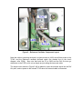
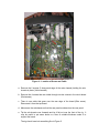
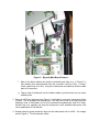
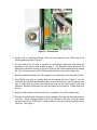
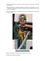
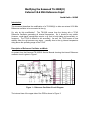
Modifying the Kenwood TS-2000(X)
External 15.6 MHz Reference Input
David Smith – VK3HZ
Introduction
This document describes the modification of a TS-2000(X) to allow an external 15.6 MHz
Reference oscillator to be connected to the rig.
So, why do this modification? The TS-2000 comes from the factory with a TCXO
Reference Oscillator generating all internal frequencies. So, it should be very stable.
However, weak-signal experiments require a rig that is both stable and accurately onfrequency. The TCXO is difficult to set accurately. As well, the TCXO seems to lose
stability when the rig becomes very warm – possibly due to the rig internal temperature
rising above the operating range of the TCXO.
Description of Reference Oscillator and Mods
An extract from the Kenwood TS-2000/X Service Manual showing the internal Reference
oscillator circuit is given in Figure 1.
Figure 1 – Reference Oscillator Circuit Diagram
The internal view of the upper side of the PCB is shown in Figure 2.
Figure 2 – Reference Oscillator Component Layout
Note that, without removing the board, we have access to L429, which filters power to the
TCXO, and the Reference oscillator buffered output (the dashed line on the circuit
diagram, after C569). Also note that both the 5V at L429 and the Ref Out also go
elsewhere on the PCB, so it’s not as simple as just cutting the trace and cable.
The simple circuit shown in Figure 3 will be added to inject the external signal into the Ref
Out point, and cut power to the internal TCXO when the external cable is connected.
Figure 3 – Circuit Modifications
The circuit uses a 2N7000 FET to switch the 5V power to the VCXO. A FET provides low
voltage drop, but has the disadvantage that the gate must be raised at least 2.1V above
the source to switch it on. Fortunately, there’s a supply of +8V nearby. The reference
source needs to have an output DC resistance of less than 1K for the switching circuit to
work properly,
Parts Required
1 – 2N7000 N-channel FET
1 – 68K 1/4W resistor
1 – 5.6K 1/4W resistor
1 – 10n 63V disk ceramic capacitor
1 – 1n 63V disk ceramic capacitor
1 – 33p 63V disk ceramic capacitor
1 – 500mm length of thin Teflon coax with your connector of choice
1 – Solder lug (3mm hole)
Modification Steps
1. Turn the rig upside down and remove the bottom cover. The top cover does not need
to be removed.
2. Now we need to move the sub-chassis holding the main circuit board out of the way.
Refer to Figure 4 in the following sub-sections.
Figure 4 – Location of Screw and Cable
a. Remove the 6 screws (3 along each edge of the main chassis) holding the subchassis in place (Yellow arrows).
b. Remove the 4 screws that are visible through circular cutouts in the circuit board
(Red arrows).
c. There is one cable that goes over the rear edge of the board (Blue arrow).
Disconnect it from the top board.
d. Manoeuvre the subchassis so that the rear panel sockets clear the rear panel.
e. Tip the sub-chassis over forwards and lay it flat out over the front of the rig. It
may be useful to put some books or a box of suitable thickness under it to
support the board.
The rig should now look something like in Figure 5.
Figure 5 – Rig with Main Board Cleared
f. Most of the ribbon cables can remain connected apart from one. In Figure 5, it
has already been disconnected from the connector circled in Red. I haven’t
found a good way to do this. Just pull to disconnect and carefully stuff the cable
back in to reconnect.
g. Tape a strip of cardboard over the ribbon cables to protect them from an errant
soldering iron.
3. Remove L429 from the board (see Figure 1), preferably in one piece, because it will be
re-used. This is probably the hardest step. The way I did it was to use two fine-point
soldering irons to heat each end of the component simultaneously and lift it away.
Another way is to carefully just snip the component in half, desolder each piece, and
use a replacement 47uH inductor.
4. Scrape away the green protective layer on the earth plane next to L429 – the orange
area in Figure 6. Tin the area with solder.
Figure 6 – Ground Area
5. Solder L429 in, standing vertically, with one end soldered to the TCXO end of the
existing pads (top pad in Figure 6).
6. Cut one lead of the 10n and 1n capacitor to 5mm length, bend them and solder the
capacitors to the ground area created in step 4. The capacitor bodies should be flat
against the aluminium housing to the left of Figure 6 with unused leads pointing straight
up. The 10n body points in the TCXO direction while the 1n points the other way.
7. Bend the unattached lead of the 10n capacitor over and solder to the free end of L429.
8. The 2N7000 now goes in vertically with the flat towards the left in Figure 6. Cut the
Drain and Source leads and bend the tips over so that the Source just touches the free
end of L429 while the Drain just touches the pad on the board where L429 was
attached. Bend the Gate lead to the left and leave for the moment. Solder Drain and
Source.
9. Solder the Gate lead to the free end of the 1n capacitor. Cut off the excess lead.
10. Thread the coaxial cable through the lower ventilation slot near the back-panel power
connector. Route it along the edge of the 70cm PA board to the front of the rig, across
the front and into the TCXO area. I used a cable tie to the ground lug connection to the
70cm PA. See Figure 7.
Figure 7 – Suggested Cable Route
11. Strip back the end of the coax, wrap the solder lug around it and solder to the braid
(hence Teflon coax is recommended). Place the solder lug under the screw (See
Figure 8)
Figure 8 – Post Modification
12. Solder the 5.6K resistor from the tip of the coax to the junction of the 1n capacitor and
the Gate of the 2N7000.
13. Solder the 68K resistor from the same junction to the pin on the connector marked 8V
(see Figure 2).
14. With the soldering iron, carefully melt away a short length of the insulation on the inner
of the Ref Out shielded cable. Solder the 33p capacitor to this and the other end to the
tip of the coaxial cable.
15. Figure 9 shows a close up. Unfortunately, the 1n and 10n capacitors are obscured by
the coaxial cable.
Figure 9 – Closeup of Modifications
16. Remove the protective cardboard and re-attach the ribbon cable.
17. Replace the main board sub-chassis.
Testing
With the bottom cover removed, and nothing connected to the Reference Input, apply
power to the rig and switch on. The rig should behave normally. You should just be able
to measure the voltage on the top of L429, which should be 4.95V or thereabouts.
Attach a 1K resistor or less across the Reference Input (or even short the connector). The
rig should stop working and show an Unlock error on the front panel. The voltage at the
top of L429 should be close to zero.
While listening to a CW signal on one of the VHF/UHF bands, connect a clean, stable 15.6
MHz source to the Reference Input. Level should be around +5 to +8 dBm (3 – 6 mW). If
all is working OK, you’ll probably notice a slight jump in frequency. Otherwise there should
be no change in signal quality.
(Reminder: the signal source must have a DC resistance to ground of 1K or less for the
switching circuit to work).