1
_
V9.12. 241
Technical Notes
NEC V850 Family On-Chip Emulation
This document is intended to be used together with the CPU reference manual provided by
the silicon vendor. This document assumes knowledge of the CPU functionality and the
terminology and concepts defined and explained in the CPU reference manual. Basic
knowledge of winIDEA is also necessary. This document deals with specifics and advanced
details and it is not meant as a basic or introductory text.
Contents
Contents
1
1 Introduction
2
2 Emulation options
2.1 Hardware Options
2.2 Initialization Sequence
2.3 JTAG Scan Speed
3
3
4
4
3 CPU Setup
3.1 General Options
3.2 Debuggging
3.3 SoC
3.4 uPD70Fxxxx
5
5
6
7
8
4 Internal Flash Programming
4.1 Program Flash
4.2 Data Flash
10
10
11
5 Security Function
13
6 Protection & Security Flags
13
7 EEPROM Emulation
16
8 Hot Attach
19
9 Real-Time Memory Access
20
10 Access Breakpoints
21
11 Emulation Notes
22
12 Getting Started
22
13 Troubleshooting
23
iSYSTEM, June 2015
1/23
1 Introduction
On-chip debug support for NEC V850 F-line family is based on the NEC N-Wire debug
interface. Some of the debug functionalities are hard coded in the on-chip debug module
while the others are implemented by custom monitor functions, loaded in a dedicated CPU
memory space and then called by the debugger.
Debug Features
Hardware execution breakpoints
Unlimited software breakpoints
Access Breakpoints
Real-time access
Program & Data Flash Programming
EEPROM Emulation Support
Security Function
iSYSTEM, June 2015
2/23
2 Emulation options
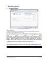
2.1 Hardware Options
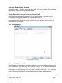
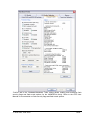
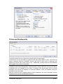
Emulation options, Hardware pane
Debug I/O levels
The development system can be configured in a way that the debug N-Wire signals are
driven at 3.3V, 5V or target voltage level (Vref).
When 'Vref' Debug I/O level is selected, a voltage applied to the belonging reference voltage
pin on the target debug connector is used as a reference voltage for voltage follower, which
powers
buffers,
driving
the
debug
N-Wire signals. The user must ensure that the target power supply is connected to the Vref
pin on the target N-Wire connector and that it is switched on before the debug session is
started. If these two conditions are not meet, it is highly probably that the initial debug
connection will fail already. However in some cases it may succeed but then the system will
behave abnormal.
It’s recommended to select 5.0V selection when the CPU operates at 5V.
Hot Attach
Option must be checked when Hot Attach is used. Refer to the Hot Attach chapter for more
details on Hot Attach use.
Note: Hot Attach function cannot be used for any flash programming or code download!
iSYSTEM, June 2015
3/23
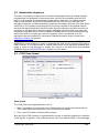
2.2 Initialization Sequence
The user must properly configure the CPU before the debug download (including the flash
programming) can take place to the memory area, which is not accessible upon the CPU
reset. This is essential for the applications using memory resources, for instance external
RAM or external flash, which are not accessible after the CPU reset. In such case, the
debugger executes a so-called initialization sequence immediately after the CPU reset, which
writes to the CPU registers configuring the CPU memory interface to the physical memory
and then the debug download is executed. Note that the initialization sequence must be set
up specific to the application. Besides enabling a disabled memory access upon reset, the
initialization sequence can be used for instance to disable the CPU internal watchdog being
active after reset or to modify any other CPU registers, when it’s preferred to run the
application with the modified CPU reset state. Detailed information may be found in the
Initialization Sequence help topic.
Note: There is no need to use the initialization sequence for the V850ES/Fx2 and
V850ES/Fx3 microcontrollers in order to download the code into the internal CPU flash or
RAM. However, it is recommended to enable read access to the data flash (disabled after
reset) in order for the debugger to display the content of the data flash and emulated
EEPROM. Refer to EEPROM Emulation chapter for more details.
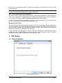
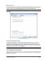
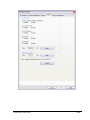
2.3 JTAG Scan Speed
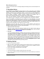
Emulation options, JTAG pane
Scan speed
The JTAG chain scanning speed can be set to:
Slow - long delays are introduced in the JTAG scanning to support the slowest devices.
JTAG clock frequency varying from 1 kHz to 2000 kHz can be set.
Fast – the JTAG chain is scanned with no delays.
Slow and Fast JTAG scanning is implemented by means of software toggling the necessary
JTAG signals. In general, Fast mode should be used as a default setting. If the debugger
iSYSTEM, June 2015
4/23
fails to work or it behaves unstable, try Slow mode at different scan frequencies until you find
a working setting.
Note: Burst, Burst+, RTCK and Free mode are not supported on the V850 N-Wire debug
interface and are automatically forced to Slow if selected.
Use – Scan Speed during Initialization
On some systems, slower scan speed must be used during initialization, during which the
CPU clock is raised (PLL engaged) and then higher scan speeds can be used in operation.
In such case, this option and the appropriate scan speed must be selected.
In case of troubleshooting initial debug connection, it’s recommended not to use this option
and try to connect to the CPU with scan speed set to low.
Number of idle TCKs
Some V850 CPUs require inserting wait states in the JTAG scanning on which N-wire debug
interface is based. Wait states are implemented by inserting extra TCKs (N-wire clock) when
the JTAG state machine goes through the Update-DR state, because within this stage the
debug data registers are updated by the CPU itself.
It has been observed that approx. 3-6 idle TCKs are necessary for working N-wire debug
interface in case of V850E/Dx3 family, which starts at ~200kHz RingOsc while for instance
V850ES/Fx3 family starts at 8MHz and requires no idle TCKs.
3 CPU Setup
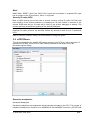
3.1 General Options
General options dialog
iSYSTEM, June 2015
5/23
Interrupts Enabled When Stopped
When this option is checked, user interrupts (NMI, INT) which are generated while the
application is stopped are accepted and processed.
When the option is unchecked, interrupts are not serviced while the application is stopped.
Cache Downloaded Code only (do not load to target)
When this option is checked, the download files will not propagate to the target memory
using standard debug download but the Target download files will.
‘Cache Downloaded Code only (do not load to target)’ option should be checked in cases,
where the application is previously programmed in the target and only symbols need to be
downloaded to the debugger.
3.2 Debuggging
Debugging options dialog
Set/clear SW BPs before Run
When the option is checked, then a software breakpoint is not set/cleared immediately, but is
just remembered. Only when the CPU is set to running are the software breakpoints
committed to the program flash. This way several breakpoints (residing in the same flash
sector/page) can be changed but only one re-flash operation takes place. This is especially
noticeable in testIDEA operation with many stubs and also during a regular debugging
session when several breakpoints are set/cleared within the same flash erase block.
iSYSTEM, June 2015
6/23
Main clock (X1, X2)
The user needs to specify the frequency of the oscillator/crystal, which is connected to the X1
and X2 CPU pins. This is the frequency at which the CPU operates after reset. This value is
used by the NEC Self-Programming libraries during the CPU flash programming.
Note: This setting applies for the V850ES/Fx2 family only.
3.3 SoC
Advanced Emulation Options
Override startup register values
For faster flash programming, the debugger engages the target MCU PLL. There are PLL
configuration related registers (CKC and PCC), which are write once register. Since the
debugger modifies them already before flash programming takes place, later writes to these
registers from the user application would have no effect. For this reason, user must enter the
CKC and PCC register values from his application.
Note: This setting is available only on V850E/Dx3 microcontrollers.
Use handshaking during download
When this option is checked, execution of every debug command during debug download is
handshaked. Faster download is achieved by unchecking the option. If the download fails,
keep the option checked.
iSYSTEM, June 2015
7/23
Mask
NMI0, NMI1, RESET, WAIT and HOLD CPU inputs can be masked. A masked CPU input
has no impact on the CPU behavior, that is, it is ignored.
Security ID code (HEX)
Most of V850 devices but not all have a security function (unlock ID code 70H-79H) that
limits starting of the N-Wire emulator by comparing an ID code written in advance to the
internal ROM area with an ID code that is input by the N-Wire debugger at startup. This
function prevents unauthorized reading of the internal ROM area.
Note: When bit 7 of address 79H is programmed to 0, N-Wire emulator use is permanently
disabled! For safety reasons, the emulator inhibits any attempt to write 0 to bit 7 at address
0x79.
Refer to ‘Security Function’ section for more details on using this option.
3.4 uPD70Fxxxx
This tab is named after the specific CPU being selected in the CPU list. In this particular it’s
named uPD70F3420, since uPD70F3420 is being selected as the target CPU in the
Emulation Options dialog.
Execution breakpoints
Hardware Breakpoints
Hardware breakpoints are breakpoints that are already provided by the CPU. The number of
hardware breakpoints is limited to 6 for V850ES/Fx2 and V850ES/Fx3 devices. µPD70F3440
iSYSTEM, June 2015
8/23
features 10 breakpoints. The advantage is that they function anywhere in the CPU space,
which is not the case for software breakpoints, which normally cannot be used in the nonwriteable memory (ROM) or self-modifying code.
Two hardware breakpoints are part of the V850ES core and are used as execution
breakpoints or as access breakpoints. Remaining breakpoints are implemented using the
ROM correction function. Note that the debugger controls and share different execution
breakpoint debug resources hidden from the user.
Note: The same on-chip debug resources are shared among two hardware execution
breakpoints and access breakpoints. Consequentially, debug resources used by one debug
functionality are not available for the other. In practice this would mean that only four
execution breakpoints can be set when there are two access breakpoints set for instance on
instruction address already.
One execution breakpoint is required by the debugger when source step debug command is
executed. For this reason, when all available hardware breakpoints are used as execution
breakpoints, the debugger may fail to execute the debug source step. The debugger offers
'Reserve one breakpoint for high-level debugging' option in the Debug/Debug
Options/Debugging' tab to circumvent this. By default, this option is checked and the user
can uncheck it anytime.
Software Breakpoints
Available hardware breakpoints often prove to be insufficient. Then the debugger can use
unlimited software breakpoints to work around this limitation.
When a software breakpoint is being used, the debugger first attempts to modify the source
code by placing a break instruction into the code. If setting software breakpoint fails, a
hardware breakpoint is set instead.
Check the ‘Use software breakpoints’ when software breakpoints should be explicitly used.
Stop CPU Activities When Stopped
When this option is checked, some peripheral functions are stopped when the application is
stopped. The following functions are stopped:
Watch timer
16-bit timer/counter
A/D converter
In general, it is recommended that the option is checked in order to have more predictable
behavior of the debugged application using these peripheral functions.
Mask NMI0, NMI1, RESET, WAIT, HOLD
NMI0, NMI1, RESET, WAIT and HOLD CPU inputs can be masked. A masked CPU input
has no impact on the CPU behavior, that is, it is ignored.
iSYSTEM, June 2015
9/23
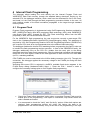
4 Internal Flash Programming
The debugger allows loading the code directly into the internal Program Flash and
V850ES/Fx3 Data Flash memory through the standard debug download. Relying on the
selected CPU, the debugger identifies, which code from the download file fits in the Flash,
and loads it to the Flash through the flash programming procedure hidden to the user. All
code residing outside of the flash boundaries propagates to the target through standard
memory writes.
4.1 Program Flash
Program Flash programming is implemented using Self-Programming libraries provided by
NEC. V850ES/Fx2 family uses NEC proprietary flash technology (UC2) while V850ES/Fx3
uses Super Flash (MF2), licensed by SST. This Flash technology differs from the NEC
proprietary in both, the cell and the block structure.
For the V850ES/Fx2 flash programming, the user must enter correctly a reset target CPU
clock in the ‘Hardware/Emulation Options/CPU Setup/Debugging’ dialog. This parameter is
required by UC2 Self-Programming libraries. MF2 Self-Programming libraries (V850ES/Fx3)
don’t require CPU clock as an input parameter due to the different flash technology.
The debugger disables the internal CPU watchdog before programming the flash in order not
to interfere the flash programming monitor execution. In case of the V850ES/Fx2 family, the
debugger additionally turns on the CPU PLL (hidden from the user) prior to the debug
download to achieve faster flash programming. After the download completes, the debugger
resets the CPU once again in order for the user application to start from the CPU reset state
(no PLL, watchdog enabled).
CPU FLMD0 pin must be connected to the N-Wire debug connector (pin A13). Through this
connection, the debugger applies the necessary voltage to the FLMD0 pin during the flash
programming.
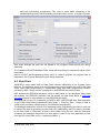
Assuming that correct CPU is selected in winIDEA, available flash device appears in the
FLASH Setup dialog (Hardware/FLASH Setup…). Press the ‘Edit…’ button in order to
configure the necessary settings prior to first Program flash programming.
Check the ‘Erase before download’ option when a complete Program Flash must be
erased prior to the programming. If the option is unchecked, only sectors where the
code is loaded are erased.
It is recommend to check the ‘Verify’ and ‘On the fly’ options. When both options are
checked, flash programming monitor will (while still having the data to be
programmed in the monitor buffer) verify at the end of the programming if the input
iSYSTEM, June 2015
10/23
data was successfully programmed. This verify is much faster comparing to the
standard Debug/Verify Download debug command, which is then no longer required.
With these settings the code can be loaded to the Program Flash through the debug
download.
The ‘Hardware/uPD70F3380/Mass Erase’ button allows erasing the complete Program Flash
individually.
Version of NEC Self-Programming library which is used to program the program flash is
displayed in the Progress dialog during the debug download.
4.2 Data Flash
V850ES/Fx3 series adds 32kB of Data Flash memory additionally to the Program Flash
memory. The debugger needs to be configured properly before loading the code to the Data
Flash. Data Flash programming is implemented using data flash programming libraries
provided by NEC. Library version is displayed in the EEPROM emulation window.
NEC implemented EEPROM emulation, which is also based on the data flash. Most users
will probably use EEPROM emulation and not directly the data flash. Refer to EEPROM
Emulation chapter for more details on using EEPROM emulation.
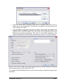
Assuming that correct CPU is selected in winIDEA, ‘NEC uPD70F33XX Data’ device appears
in the FLASH Setup dialog (Hardware/FLASH Setup…). Press the ‘Edit…’ button in order to
configure the necessary settings prior to first Data flash programming.
The debugger disables the internal CPU watchdog before programming the flash in order not
to interfere the flash programming monitor execution. Additionally, the CPU memory interface
to the Data Flash is configured. All this is done hidden from the user. After the download
completes, the debugger resets the CPU once again in order for the user application to start
from the CPU reset state (no PLL, watchdog enabled…).
iSYSTEM, June 2015
11/23
Check the ‘Erase before download’ option when a complete Data Flash must be
erased prior to the programming. If the option is unchecked, only sectors where the
code is loaded are erased.
It is recommend to check the ‘Verify’ and ‘On the fly’ options. When both options are
checked, flash programming monitor will (while still having the data to be
programmed in the monitor buffer) verify at the end of the programming if the input
data was successfully programmed. This verify is much faster comparing to the
standard Debug/Verify Download debug command and is then no longer necessary.
Now the code can be loaded to the Data Flash through the debug download. Valid Data
Flash region after reset is 0xFF 8000-0xFF FFFF.
The ‘Hardware/uPD70F3380/Mass Erase’ button allows erasing the complete Program Flash
individually.
iSYSTEM, June 2015
12/23
Note: Data flash is not visible after the CPU reset. Read access to the Data flash is enabled
through the DFLCTL register. Note that writing to this register is protected by a special
sequence of instructions.
In order to see the Data flash after reset, the user can create an .ini file which enables a read
access after the CPU reset. The initialization sequence use is described in the Initialization
Sequence help topic. An example of the ini file which enables the read access to the Data
flash:
A PRCMD B 0x5A
A DFLCTL B 0x83
5 Security Function
V850ES/Fx2 and V850ES/Fx3 families contain a so called Rom Security Unit (RSU). Without
unlocking the RSU any read access to the CPU resources such as register, SFR and
memory is not permitted. The RSU limits starting of the N-Wire emulator by comparing an ID
code written in advance to the internal ROM area with an ID code, that is input by the N-Wire
debugger at the startup. This function prevents a third party from reading the internal ROM.
The area of the ID code is 10 bytes wide and is located in the address range 0x70-0x79.
When the memory is erased, the ID code contains all 0xFFs.
For the user’s convenience, it is recommended to use all FFs for the N-Wire unlock ID code
during the debugging. If the user programs specific ID code and accidentally forget it, the
debugger can no longer be connected the CPU - unless the complete flash is erased with the
NEC flash programmer. In order not to accidentally change the ID code through the debug
download, the debugger also omits writing to 0x70-0x79 memory area during the debug
download.
In order to modify the security ID in the CPU Flash, the user needs to enter the ID (e.g. FF
FF 32 17 A5 FF 88 FF FF FF) in the ‘SoC’ tab first, and then press Hardware/Flash->Secure.
This will program custom ID in the flash. After next reset, the debugger uses the new ID code
in order to unlock the N-WIRE. Make sure you don’t forget the ID code after you write a new
one through the Secure function. N-Wire debug interface cannot be unlocked if the ID code
doesn’t match with the one in the internal ROM/Flash.
There is additional security bit, bit 7 at address 0x79. When this bit is programmed to 0, NWire emulator use is disabled permanently. For safety reasons, winIDEA inhibits any write to
bit 0 at address 0x79. If the customer requires writing the bit 7, iSYSTEM support should be
contacted for the assistance.
6 Protection & Security Flags
This functionality is not available for all V850 devices. Due to the nature of these flags,
double check before applying a new value. Incorrect value may yield a flash or the CPU
inaccessible through the on-chip debug interface.
‘Program FLASH’ tab in the ‘Hardware/Hardware Tools’ dialog displays CPU information and
allows reading and modifying program flash protection flags for the V850ES/Fx3 family. Refer
to the CPU User Manual for more details on specific V850ES/Fx3 protection flags settings.
iSYSTEM, June 2015
13/23
‘FLASH’ tab in the ‘Hardware/Hardware Tools’ dialog allows reading and modifying flash
security flags and flash mask options for the V850E2/Fx4 family. Refer to the CPU User
Manual for more details on flash security flags and flash mask options.
iSYSTEM, June 2015
14/23
iSYSTEM, June 2015
15/23
7 EEPROM Emulation
As an alternative to the classical EEPROMs, where the data is stored on a fixed address and
so can always be found on the same location, NEC implemented EEPROM emulation, where
the data is stored on changing locations. Note that the EEPROM emulation is based on the
data flash memory. Refer to NEC documentation to get familiar with the EEPROM terms and
the EEPROM emulation itself.
Data FLASH and EEPROM Emulation window is available through the ‘Hardware/Tools’
menu.
iSYSTEM, June 2015
16/23
EEPROM Emulation debug window supports two EEPROM layouts: default 2 x 4000h (two
sections each 16K) and 2 x 2000h (two sections each 8KB and 16KB remains for the data
flash). Application EEPROM layout is configured through the ‘Emulation Mode’ combo box.
Note that after the CPU reset, the V850ES/Fx3 data flash is not visible and it’s up to the user
to enable the data flash read access before using the data FLASH and the EEPROM
Emulation window. An example of winIDEA .ini file which enables read access to the Data
flash:
A PRCMD B 0x5A
A DFLCTL B 0x83
All EEPROM and Data flash management is done using NEC DFALib and EEELib libraries.
A version of both libraries is displayed in the Data FLASH and EEPROM Emulation window.
Available emulated EEPROM use cases:
Erase on download
Check the ‘Erase on download’ option in order to erase the data flash prior to debug
download.
Erase on request
Press the ‘Erase now’ button in order to erase the data flash manually
Load on download
Check the ’Load on download’ option and specify the file to be loaded into the
emulated EEPROM. The file format must comply with the NEC specification of raw
data format for emulated EEPROM.
Load on request
Specify the file to be loaded to the emulated EEPROM and press the ’Load now’
button. The file format must comply with the NEC specification of raw data format for
emulated EEPROM.
Upload data
reads out the complete content of the Data flash and emulated EEPROM and
displays it. EEPROM section of the window displays all data sets and Data Flash
section displays Data flash memory including ID tags, where Section header, Data
zone and ID zone can be inspected too. Note that addresses in the Data FLASH
section are relative to the Data flash base address.
Single ID write
adds new data set to the existing ones. The user must write the data in the Data field,
specify belonging 16-bit ID and 16-bit Length parameter and then press Write.
Single ID invalidate
Specify the ID of the data set to be deleted and press the ‘Invalidate’ button. It is
equivalent to specifying Length=0, entering empty Data and clicking the Write button.
Save on request
Specify the file where the EEPROM content is to be stored and press the ‘Save now’
button in order to save the current EEPROM content. The generated file is compliant
with the NEC specification of raw data format for emulated EEPROM. Existing file
generation assumes default 0x4000 section size. Contact iSYSTEM if the application
uses different EEPROM section size.
Auto save
Specify the file where the EEPROM content is to be stored and check the ‘Auto save’
option.
This functionality is required for the in-circuit emulator based debugging sessions that
are continued after a power off. In case of the in-circuit emulator, data flash
respectively emulated EEPROM is emulated by the FPGA and thereby its content is
lost when the system is powered off. Before the winIDEA session ends, current
iSYSTEM, June 2015
17/23
EEPROM content can be automatically saved in the file and later on loaded through
the use of Load on download use case. Following actions are treated as a session
end: Tools/Disconnect, File/Workspace/Close, winIDEA exit and Debug/Download.
The generated file is compliant with the NEC specification of raw data format for
emulated EEPROM. Existing file generation assumes default 0x4000 section size.
Contact iSYSTEM if the application uses different EEPROM section size.
REMARKS:
Due to a lenghty refresh process, the EEPROM Emulation display is refreshed on demand
only. On these two exceptions however, it is refreshed automatically:
after download
after modifying its contents in the EEPROM Emulation window using Single ID write,
Single ID delete, Erase on request or Load on request use cases.
The EEPROM data to be loaded into the emulated EEPROM must be specified in a text file,
which complies with NEC EEPROM raw data format. Refer to NEC documentation for more
details on the EEPROM raw data format.
An excerpt from a sample file defining a single data set with ID=0x0101 and Length=0x14:
File{
AdministrativeSection{
SectionSize: 0x4000
Offset: 0x00
}
Record{
ID: 0x0101
Length: 0x14
Data: 0x00, 0x06, 0x01, 0x0C,
// (4 bytes)
0x00, 0x00, 0xFF, 0xFF,
// (4 bytes)
0x00, 0x12,
// (2 bytes)
0x00, 0x48,
// (2 bytes)
0x00, 0x06, 0x00, 0x00,
// (4 bytes)
0x90, 0xFB, 0xFF, 0xFF
// (4 bytes)
}
}
Emulated EEPROM can be also programmed through the data flash. More directly data flash
related functions are available in the bottom half of the dialog.
Load on download
Check the ’Load on download’ option and specify the file to be loaded into the data
flash. The file format is Intel-Hex format while the file content must comply with the
NEC specification. First half of the file content represents a directly memory
addressable data and the 2nd half represents the belonging ID Tag for each 32-bit
data.
Load on request
Specify the file to be loaded to the data flash and press the ’Load now’ button.
Save on request
Specify the file where the data flash content (including ID tags) is to be saved and
press the ‘Save now’ button in order to save the current data flash content. The
generated file format is configurable and can be Motorola-S, Intel-Hex or binary
format. File content structure is the same as the one described under the ‘Load on
download’.
iSYSTEM, June 2015
18/23
8 Hot Attach
V850 N-Wire debug support includes a Hot Attach function, which allows the emulator to
connect to a working target device and have all debug functions available. As such, it is a
very convenient troubleshooting tool when the application misbehaves after a longer time.
The user can connect to and inspect such an application after the problem pops-up.
Requirements:
1K ohm pull-up must be added on the DRST CPU pin, which keeps the DRST level at
high level when the N-Wire debugger is disconnected from the debugger. Pull-up
should not have a higher value since there is also an internal pull-down on this line. If
there is additionally an external pull-down it is recommended to remove it. Do note
that the application will not start in standalone (user) mode with the DRST pull-up.
Hence, it is recommended to connect this pull-up over a jumper, which is set when
the debugger is used and removed when the application is started in a standalone
(user) mode.
The target application must be started with the N-Wire debugger connected since the
on-chip debug module (RCU1 macro) is enabled at the moment when the CPU reset
line is released. Hot Attach is not supported when the application is not started with
the RCU1 macro enabled.
A typical scenario looks like this. The application is started through the standard debug
session, which enables on-chip RCU1 macro and then the debugger can be disconnected.
Later, when the target starts exhibiting problems, the tool can be connected again without
stopping or resetting the CPU. This allows an inspection into the application without intrusion.
However, note that there must be no external CPU reset in between as this disables RCU1
macro and then the debugger can no longer connect to the CPU without resetting the CPU.
The procedure for Hot Attach:
1. Start the application through the standard winIDEA debug session. End winIDEA session
(e.g. Tools/Disconnect or simply close the workspace) and disconnect the N-Wire debug
iCard from the debug connector. The target application should be running now with the
on-chip RCU1 macro enabled.
2. Select the ‘Hot Attach’ option in the ‘Hardware/Emulation Options/Hardware’ tab.
3. Perform debug download without N-Wire debug cable connected. The debugger will be
initialized and the ATTACH status will be shown.
4. Select the ‘Attach’ debug command in the Debug menu.
5. You’ll be requested to connect the N-Wire debug cable. Make sure that you first establish
a separate ground connection between the ic3000HS emulator (ground pin is available
on the front side) and the target. Otherwise, a running target may reset when connecting
the N-Wire debug cable to the target debug connector. After connecting the grounds
firsts, connect the N-wire debug cable and press OK. The emulator will try to connect to
the on-chip RCU1 macro. If it is successful, it shows the STOP or RUNNING status. At
this point, all debug functions are available.
6. When the debugging is finished, select Detach from the Debug menu. The status shown
is ATTACH and the application should be running again. Now the N-Wire debug cable
can be safely removed.
Note: Hot Attach function cannot be used for any flash programming or code download!
iSYSTEM, June 2015
19/23
9 Real-Time Memory Access
N-wire real-time access is implemented with an intrusion on the application execution. Let’s
name it run-time access in order not to mix it with iSYSTEM alternative real-time access
available on V850ES/Fx3 ICE solution. It takes approximately 50 clocks to execute a single
32-bit real-time memory read, yielding 5µs stop at 10MHz CPU clock. More the expressions
are run-time updated, more the application is stalled. It has been confirmed that the
application ceases to work properly due to enabled run-time access when putting for
instance a large structure in the Real-time Watch pane. Thereby, the user should use runtime access with caution or use iSYSTEM in-circuit emulator where an alternative solution is
available without stalling the CPU.
Run-time access cannot be performed together with the break function such as hardware
execution breakpoint supported in the CPU and software break (DBTRAP instruction), etc. It
is recommended that run-time access is disabled by default. Use run-time access while being
fully aware of its restrictions.
Watch window’s Rt.Watch panes can be configured to inspect memory in run-time. Run-time
access is enabled in the ‘Debug/Debug Options/Memory Access’ tab and in the
‘Debug/Debug Options/Update’ tab. Further, memory and SFR window can be configured to
be updated in run-time too.
iSYSTEM, June 2015
20/23
10 Access Breakpoints
Two break events can be configured to stop the CPU on data access.
A break event can be restricted to a specific ASID value when MMU is used. The CPU can
break on address match or mismatch. Access type can be read, write or read/write and
access size can be 8-bit, 16-bit, 32-bit or any. Additionally, a break event can be conditional
with the data value match or mismatch.
Note: The same on-chip debug resources are shared among two hardware execution
breakpoints and access breakpoints. Consequentially, debug resources used by one debug
functionality are not available for the other. In practice this would mean that no access
breakpoint can be set for instance on instruction address, when all available execution
breakpoints are set already.
Real-time access must be disabled when access breakpoints are used. Otherwise, access
breakpoints may exhibit unpredictable behavior.
iSYSTEM, June 2015
21/23
When Breakpoints Occur
A beep can be issued and/or a message displayed indicating that an access breakpoint has
occurred.
11 Emulation Notes
The V850ES/Fx2 and V850ES/Fx3 devices feature an 8-bit on-chip debug mode (OCDM)
register, which specifies whether dedicated pins of the microcontroller operate in normal
operation mode (port mode or alternative mode) or can be used for on-chip debugging (NWire interface). The setting of this register concerns only those pins that can be used for the
N-Wire interface: P05/DRST, P52/DDI, P53/DDO, P54/DCK and P55/DMS. Refer to
Microcontroller Reference Manual for more details on the OCDM register.
Note: If the pins P05/DRST, P52/DDI, P53/DDO, P54/DCK and P55/DMS are used as NWire interface pins their configuration cannot be changed by the pin configuration registers.
After external RESET, the dedicated pins are available for on-chip debugging. If the user
wants to use P05, P52, P53, P54 and P55 as I/O ports in his application, the application
should write OCDM.OCDM = 0. However, note that this disables the V850ES/Fx2 N-Wire
interface. In case of V850ES/Fx3 family, the application cannot modify OCDM.OCDM to 0 as
long as the N-Wire debugger is connected to the microcontroller.
Applications using P05, P52, P53, P54 and P55 in normal operation mode cannot be
debugged through the N-Wire interface. An in-circuit emulator must be used to debug such
applications without losing P05, P52, P53, P54 and P55 ports.
Cautions on Real Time Access
Real time access cannot be performed together with the break function such as
hardware execution breakpoint supported in the CPU and software break (DBTRAP
instruction), etc. See Real-Time Access chapter for more details.
Interrupts
For more predictable debugging, maskable interrupt requests are disabled during source
step debug command. For instance, if there would be a periodical interrupt (e.g. timer),
the program would keep entering in the interrupt routine with every source step if
interrupts would not be disabled. Consequentially, it is not allowed to step over the
source line or function, which changes the interrupt flag in the PSW (Program Status
Word) register or the PSW register could have a wrong value after the source step. The
program must be run over such parts of code. It is also recommended to check the ‘Stop
CPU Activities When Stopped’ option in the ‘CPU Setup/Options tab’ for more
predictable interrupt behavior during the debug session.
12 Getting Started
Connect the development system
Make sure that the target debug connector pinout matches with the one requested by a
debug tool. If it doesn't, make some adaptation to comply with the standard connector
otherwise the target or the debug tool may be damaged.
Power up the emulator and then power up the target.
Execute debug reset
The CPU should stop on location to which the reset vector points
Open memory window at internal CPU RAM location and check whether you are able to
modify its content.
iSYSTEM, June 2015
22/23
If you passed all 6 steps successfully, the debugger is operational and you may proceed
to download the code.
13 Troubleshooting
If the debugger cannot connect to the CPU, try to select 5.0 V for the N-Wire debug I/O
levels and see if it makes any difference.
If the debugger loses control over the CPU after the application is run, check whether the
CPU watchdog is serviced properly. Try once to run the application by first disabling the
watchdog.
Try ‘Slow’ JTAG Scan speed if the debugger cannot connect to the CPU or behaves
unreliably.
Check that Hot Attach option is unchecked in the ‘Hardware/Emulation Options/hardware’
tab unless Hot Attached is used.
If the debug download doesn’t work reliably, make sure that ‘Use Handshaking during
download’ option is checked in the Hardware/Emulation Options/CPU Setup/Advanced’
tab.
Make sure that the power supply is applied to the target N-Wire debug connector when
‘Target VCC’ is selected for Debug I/O levels in the ‘Hardware/Emulation
Options/Hardware’ tab, otherwise emulation fails or may behave unpredictably.
When performing any kind of checksum, remove all software breakpoints since they may
impact the checksum result.
Question: I can download the program and run the application. Then I disconnect the
debugger via Tools/Disconnect and then physically disconnect the V850 debug iCARD
while the target is still powered. At that moment, the target application stops running.
Why?
I
would
need
the
target
keep
running.
Answer: This requirement is a part of the Hot Attach operation. Read the Hot Attach
chapter for more details on hardware requirements (DRST line needs 1K pull-up) and Hot
Attach use.
Disclaimer: iSYSTEM assumes no responsibility for any errors which may appear in this
document, reserves the right to change devices or specifications detailed herein at any time
without notice, and does not make any commitment to update the information herein.
iSYSTEM. All rights reserved.
iSYSTEM, June 2015
23/23