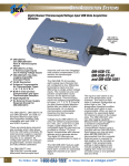
1
CIO-DAS16/M1
User’s Manual
Revision 4
May, 2000
Your new Measurement Computing product comes with a fantastic extra —
Management committed to your satisfaction!
Thank you for choosing a Measurement Computing product—and congratulations! You own the finest, and you can now enjoy
the protection of the most comprehensive warranties and unmatched phone tech support. It’s the embodiment of our mission:
To provide data acquisition hardware and software that will save time and save money.
Simple installations minimize the time between setting up your system and actually making measurements. We offer quick and
simple access to outstanding live FREE technical support to help integrate MCC products into a DAQ system.
Limited Lifetime Warranty: Most MCC products are covered by a limited lifetime warranty against defects in materials or
workmanship for the life of the product, to the original purchaser, unless otherwise noted. Any products found to be defective in
material or workmanship will be repaired, replaced with same or similar device, or refunded at MCC’s discretion. For specific
information, please refer to the terms and conditions of sale.
Harsh Environment Program: Any Measurement Computing product that is damaged due to misuse, or any reason, may be
eligible for replacement with the same or similar device for 50% of the current list price. I/O boards face some harsh
environments, some harsher than the boards are designed to withstand. Contact MCC to determine your product’s eligibility for
this program.
30 Day Money-Back Guarantee: Any Measurement Computing Corporation product may be returned within 30 days of
purchase for a full refund of the price paid for the product being returned. If you are not satisfied, or chose the wrong product by
mistake, you do not have to keep it.
These warranties are in lieu of all other warranties, expressed or implied, including any implied warranty of merchantability or
fitness for a particular application. The remedies provided herein are the buyer’s sole and exclusive remedies. Neither
Measurement Computing Corporation, nor its employees shall be liable for any direct or indirect, special, incidental or
consequential damage arising from the use of its products, even if Measurement Computing Corporation has been notified in
advance of the possibility of such damages.
Trademark and Copyright Information
Measurement Computing Corporation, InstaCal, Universal Library, and the Measurement Computing logo are either trademarks
or registered trademarks of Measurement Computing Corporation. Refer to the Copyrights & Trademarks section on
mccdaq.com/legal for more information about Measurement Computing trademarks. Other product and company names
mentioned herein are trademarks or trade names of their respective companies.
© 2000 Measurement Computing Corporation. All rights reserved. No part of this publication may be reproduced, stored in a
retrieval system, or transmitted, in any form by any means, electronic, mechanical, by photocopying, recording, or otherwise
without the prior written permission of Measurement Computing Corporation.
Notice
Measurement Computing Corporation does not authorize any Measurement Computing Corporation product for use
in life support systems and/or devices without prior written consent from Measurement Computing Corporation.
Life support devices/systems are devices or systems that, a) are intended for surgical implantation into the body, or
b) support or sustain life and whose failure to perform can be reasonably expected to result in injury. Measurement
Computing Corporation products are not designed with the components required, and are not subject to the testing
required to ensure a level of reliability suitable for the treatment and diagnosis of people.
© Copyright 2000, Measurement Computing Corp.
HM CIO-DAS16_M1.docII
Table of Contents
1. SOFTWARE INSTALLATION .........................................................................................................................................................1
2. HARDWARE INSTALLATION ........................................................................................................................................................1
2.1 BASE ADDRESS ............................................................................................................................................................................1
2.2 USER-COUNTER CLOCK/CHAINING JUMPERS......................................................................................................................2
2.3 PACER CLOCK SOURCE SELECT JUMPER..............................................................................................................................2
2.4 INSTALLING THE CIO-DAS16/M1 IN THE COMPUTER .........................................................................................................3
2.5 PROGRAMMABLE RANGE AND GAIN SETTING ...................................................................................................................3
3. SIGNAL CONNECTIONS..................................................................................................................................................................4
3.1 INTRODUCTION ...........................................................................................................................................................................4
3.2 ANALOG CONNECTOR DIAGRAM............................................................................................................................................4
3.2.1 Analog Inputs ............................................................................................................................................................................5
3.2.2 Connecting Analog Inputs.........................................................................................................................................................5
1.1.3 Shielding ...................................................................................................................................................................................5
1.1.4 Grounded Signal Source ...........................................................................................................................................................5
1.1.5 Floating Signal Source..............................................................................................................................................................6
1.1.6 Avoiding Ground Loops ............................................................................................................................................................6
1.3 DIGITAL OUTPUTS & INPUTS....................................................................................................................................................7
1.3.1 Digital Output Connector .........................................................................................................................................................7
1.3.2 Counter Clock Jumper ..............................................................................................................................................................7
1.3.3 Cabling the Digital Connector..................................................................................................................................................7
4. REGISTER ARCHITECTURE........................................................................................................................................................10
4.1 DATA TRANSFERS .....................................................................................................................................................................10
4.2 FIFO DATA BUFFER...................................................................................................................................................................10
4.3 CHANNEL/GAIN QUEUE ...........................................................................................................................................................10
4.4 CHANNEL/GAIN MEMORY CONTENTS REGISTER .............................................................................................................11
4.5 DT-CONNECT ..............................................................................................................................................................................12
4.6 CONTROL & DATA REGISTERS...............................................................................................................................................12
4.6.1 A/D Data & Channel Registers ...............................................................................................................................................14
4.6.2 Control & Status Bits ..............................................................................................................................................................14
4.6.3 Four-Bit Digital I/O Registers ................................................................................................................................................15
4.6.4 Clear Interrupt Status Register ...............................................................................................................................................16
4.6.5 Interrupt Control, Pacer Source Register ...............................................................................................................................16
4.6.6 Channel Gain Queue Address Register...................................................................................................................................17
4.6.7 Channel Gain Queue Data Register........................................................................................................................................18
4.6.8 Total Counter Data & Control Registers ................................................................................................................................19
4.6.9 Digital I/O and Counter Control & Data Registers ...............................................................................................................20
4.6.10 82C55 Digital I/O Registers..................................................................................................................................................21
4.6.11 COUNTER CHIP (82C54) ....................................................................................................................................................23
5. SPECIFICATIONS............................................................................................................................................................................24
6. ELECTRONICS AND INTERFACING..........................................................................................................................................27
6.1 COMMON MODE.........................................................................................................................................................................27
6.2 COMMON MISUNDERSTANDINGS .........................................................................................................................................28
6.3 GROUND LOOPS .........................................................................................................................................................................28
6.4 PULL UP & PULL DOWN RESISTORS .....................................................................................................................................28
6.5 TTL TO SOLID STATE RELAYS................................................................................................................................................29
6.6 VOLTAGE DIVIDERS .................................................................................................................................................................30
6.7 LOW PASS FILTERS ...................................................................................................................................................................32
iii
This page is blank.
iv
1. SOFTWARE INSTALLATION
The board has a variety of switches and jumpers to set before installing the board in your computer. By
far the simplest way to configure your board is to use the InstaCalTM program provided as part of your
software package. InstaCalTM will show you all available options, how to configure the various switches
and jumpers to match your application requirements, and will create a configuration file that your
application software (and the Universal Library) will refer to so the software you use will automatically
know the exact configuration of the board.
Please refer to the Software Installation Manual regarding the installation and operation of InstaCalTM.
The following hard copy information is provided as a matter of completeness, and will allow you to set
the hardware configuration of the board if you do not have immediate access to InstaCalTM and/or your
computer
2. HARDWARE INSTALLATION
The CIO-DAS16/M1 has one bank of base address switches and four jumpers to set before installation of
the board in your computer.
2.1 BASE ADDRESS
Unless there is already a board in your system which uses address 300h (768 decimal), leave the switches
as they are set at the factory. In the example shown in Figure 2-1, the CIO-DAS16/M1 is set for base
address 300h.
Figure 2-1. Base Address Switch
1
2.2 USER-COUNTER CLOCK/CHAINING JUMPERS
The CIO-DAS16/M1 has three counters available to the user at the digital connector, P5. (A fourth
counter is available at the analog connector, P1.) The three digital-connector counters are associated with
registers Base + 404, +405, and +406.
User-Counter 0 can be externally clocked by a jumper at JB2. It is adjacent to the digital connector and
connects the internal 10 MHz OSC signal to Counter 0 clock input (Figure 2-2). Using two additional
jumpers at JB2, the counters can be chained 0 to1, and 1 to 2 to yield counters of 32 or 48 bits. These
counters can also be chained externally at the 40-pin digital connector, P5.
JB2
OSC
C0 (CLK 0)
The on-board 10 MHz OSC signal can be connected
directly to the clock of CTR 0 by jumping OSC to C0.
O0 (OUT 0)
C1 (CLK 1)
The output of CTR 0 (O0) can be chained directly to
the clock of CTR 1 (C1).
O1 (OUT 1)
C2 (CLK 2)
The output of CTR 1 (O1) can be chained directly to
the clock of CTR 2 (C2).
Figure 2-2. User-Counter Clock Source and Chaining Jumpers
2.3 PACER CLOCK SOURCE SELECT JUMPER
When using the internal clock for pacing, select the desired frequency of the source supplied to the pacer
counters by setting the XTAL jumper for either 1 or 10 MHz (Figure 2-3). In most cases, 10MHz is the
appropriate choice. Use the 1MHz option only if you are using the CIO-DAS16/M1 with software
designed for the DAS16 (which would calculate pacer speed based on a 1MHz sourc to the pacer
counters).
1 MHz
10
XTAL
Figure 2-3. Pacing Counter Frequency-Select Jumper
2
2.4 INSTALLING THE CIO-DAS16/M1 IN THE COMPUTER
1. Turn the power off.
2. Remove the cover of your computer. Please be careful not to dislodge any of the cables installed on the
boards in your computer as you slide the cover off.
3. Locate an empty expansion slot in your computer. If you plan to use the 24 bits of digital or three
counters accessible through the rear connector, you should install the board in a slot with an available
adjacent slot for the BP40-37 connector-cable-backplate assembly.
4. Push the board firmly down into the expansion bus connector. If it is not seated fully it may fail to
work and could short circuit the PC bus power onto a PC bus signal. This could damage the motherboard
in your PC or the board.
2.5 PROGRAMMABLE RANGE AND GAIN SETTING
The analog input range is fully programmable. There are no switches to set.
The board has a channel/gain queue, that is programmed to align a channel and gain in a programmed
channel scan sequence. Channel/Gain queue loading is handled by the Universal Library programming
language library and by application programs which support the CIO-DAS16/M1.
Setting the channel gain queue is required prior to making any measurements with the CIO-DAS16/M1 so
the concept of a default range value is meaningless.
3
3. SIGNAL CONNECTIONS
3.1 INTRODUCTION
There are three connectors on th CIO-DAS16/M1. The 37-pin connector, P1, on the rear mounting plate is
primarily for analog signals. It is referred to as the analog connector. The 40-pin header connector, P5, at
the front of the board has 24 digital I/O lines. It also has clock, gate, and output signals for three counters
associated with registers Base + 404, +405, and +406. It is referred to as the digital connector.
The DT-Connect connector (P4) at the top of the board is included primarily for use with the MEGAFIFO huge sample buffer, which may be required to attain the maximum acquisition rate.
3.2 ANALOG CONNECTOR DIAGRAM
The CIO-DAS16/M1 analog connector is a 37-pin, D-type connector accessible from the rear of the PC
on the expansion backplate. The connector accepts female 37-pin D-type connectors, such as the C37FF2, a 2-foot cable. The Counter 0 signals are associated with the register at Base + C.
The CTR 2 OUT signal is the internal PACER signal (registers at Base + D, +E, and +F.)
Figure 3-1. Analog Connector Pin Out
If frequent changes to signal connections or signal conditioning is required, please refer to the information
on the CIO-MINI37, CIO-TERMINAL, or SCB-37 screw terminal board.
4
3.2.1 Analog Inputs
The CIO-DAS16/M1 has eight differential analog input channels. Each channel has a signal-high input
and a signal-low input. The measurement made by the A/D is the voltage difference between the LOW
and HIGH inputs. Differential inputs have a common mode range (see application note). The CIODAS16/M1 can have as much as 10V of common mode voltage between LLGND and signal LOW.
CAUTION
Measure the voltage between the ground signal at the signal source and the PC. Use a voltmeter and
place the red probe on the PC ground and the black probe on the signal ground. If there is more than 10
volts, do not connect the CIO-DAS16/M1 to this signal source because you will not be able to make any
reading. If the voltage is over 20V, DO NOT connect this signal because it will damage the board .
3.2.2 Connecting Analog Inpu ts
Connect analog inputs as shown in Figure 3-2 below. Pay close attention to cabling and grounding of the
shield. Failure to cable as shown will result in signal noise.
NOTE: Failure to cable as recommended will cause less than perfect readings. Perform signal wiring with
consideration to the high speeds involved. Even if your A/D pacing rate is not high, the converter is
always converting at less than 1µs and the internal MUX switching is done at a similar high speed.
NOTE: Keep high and low wires together. Keep the signal wires for a channel together. Ideally, they
should be a twisted pair. This will aid the differential inputs in rejecting EMI or RFI from input signals.
3.2.3 Shielding
To further protect the input signals from noise, use shielded cable. Shielded twisted-pair cable is readily
available. Connect the shield as in the diagrams below or ground loops and signals noise may result.
3.2.4 Grounded Signal Source
A grounded signal source has the low signal referenced to chassis ground. If an instrument has only two
poles, HI and LOW, it is probably referenced to chassis ground internally. Check with an Ohmmeter
between LOW and the power cord ground prong. If an instrument has three poles, a HI, LOW and GND,
you can strap LO to GND as shown here, or use the connection for Floating Signal Source.
5
CIO-DAS16/M1/16
Instrument
Shielded Cable
Signal High
Channel # High
Signal Low
Channel # Low
Tie Low to GND
LLGND
GND
GROUNDED SIGNAL SOURCE - Suggested way to connect
signal and cable shield. Ground is completed through
power ground. Voltage between outlet grounds not to
exceed the common mode range.
Figure 3-2. Cable Shield Grounding
3.2.5 Floating Signal Source
A floating signal source is defined as the low signal having no reference to earth ground (PC Chassis
ground or LLGND). Examples are a battery, an isolated precision power supply or a sensor which is not
earth grounded. See Figure 3-3 for a connection diagram.
Shielded
Cable
CIO-DAS16/M1/16
Signal High
Channel # High
Signal Low
Channel # Low
10K
LLGND
FLOATING SIGNAL SOURCE - Suggested way to connect signals
and cable shield. Connection is made to Earth ground through
power ground.
Figure 3-3. Floating Signal Source Referenced to Ground
A reference between signal LOW and LLGND must be provided because board inputs are differential.
Failure to supply the reference (10K resistor) will result in unrepeatable readings.
3.2.6 Avoiding Ground Loops
Figure 3-4 shows the wrong way to connect a floating signal and create a ground loop. Any current
caused by a voltage potential between the grounds will be sufficient to interfere with signal readings
6
Instrument
CIO-DAS16/M1/16
Shielded Cable
Signal High
Channel # High
Signal Low
Channel # Low
LLGND
Ground Loop Created Here
WRONG WAY! - This is the wrong way to connect cable shield.
Figure 3-4. Wrong Way to Connect a Signal
3.3 DIGITAL OUTPUTS & INPUTS
All the digital outputs and inputs on the CIO-DAS16/M1 are TTL level. TTL is an electronics industry
term, short for Transistor Transistor Logic, which describes a standard for digital signals which are either
at 0V or 5V (nominal).
To control or sense any device other than TTL IC chips, please use appropriate signal conditioning, such
as solid state relays or electromechanical relays. See the Measurement Computing catalog for SSRRACK24 and CIO-ERB24 interface accessories.
3.3.1 Digital Output Connecto r
A second connector at the rear of the board contains signals from one 82C55 and one 82C54. The 24 bits
of digital I/O (82C55) and nine counter/timer signals (from three counters of an 82C54) are available to
the user for on/off control, pulse width and frequency measurement and general counting.
The 82C54 is a 10MHz (max) down-counter chip having three 16-bit counters. The input, gate and output
signals of the counters are brought out to the connector and on-board clock-select and chaining jumpers.
Together, the 24 digital I/O, and the counters use eight I/O addresses. The lower four (Base + 400,
through +403 are used for the 82C55 digital I/O and the upper four (Base + 404 through +407) are used
for the 82C54 user-counter timer.
3.3.2 Counter Clock Jumper
The board has a row of three jumpers adjacent to P5 that allow the 10 MHz [XTAL] OSCillator signal to
be connected to counter 0 input, and the counters to be chained 0 to1, and 1 to 2. In this way, a counter of
32 or 48 bits can be constructed from the three 16-bit counters of the 82C54. The counters can also be
chained externally via the 40-pin connector.
3.3.3 Cabling the Digital Conn ector
The digital/counter connector is a 40-pin header located at the rear of the CIO-DAS16/M1 board. It is
pinned out such that when connected to a 37-pin connector via a BP40-37, the 37-pin connector's pin-outs
are nearly identical to that of the CIO-DIO24/CTR3 (Figure 3-5). When using the BP40-37, the
digital/counter I/O connector is a 37-pin D-type connector accessible from the rear of the PC through the
7
expansion backplate. If you need compatibility with this product, we recommend that you purchase the
BP40-37 cable when using the digital connector, P5.
If compatibility with the CIO-DIO24/CTR3 is not required, you can make direct connection to a CIOMINI40 screw terminal board using a C40FF-2 cable.
The signals available are direct connections to an 82C55 digital I/O chip and an 82C54 counter chip.
Figure 3-5 is the pin out of a BP40-37 connected to the digital/counter connector.
Figure 3-6 is the pin out of P5.
Figure 3-5. Digital Connector - Pin Out of BP40-37
8
NC
NC
PORT A0
PORT A1
PORT A2
PORT A3
PORT A4
PORT A5
PORT A6
PORT A7
PORT C0
PORT C1
PORT C2
PORT C3
PORT C4
PORT C5
PORT C6
PORT C7
GND
+5VDC
40
38
36
34
32
30
28
26
24
22
20
18
16
14
12
10
8
6
4
2
39
37
35
33
31
29
27
25
23
21
19
17
15
13
11
9
7
5
3
1
NC
CLK0
GATE0
THESE THREE USER-COUNTERS
OUT0
ARE ASSOCIATED WITH
CLK1
REGISTERS AT BASE +404, +405,
GATE1
+406, and +407.
OUT1
CLK2
GATE2
OUT2
PORT B0
PORT B1
PORT B2
PORT B3
PORT B4
PORT B5
PORT B6
PORT B7
NC
NC
(Beveled-corner silk-screened on board)
Figure 3-6. 40-Pin Digital Connector (P5) Pin Out
9
4. REGISTER ARCHITECTURE
4.1 DATA TRANSFERS
The CIO-DAS16/M1 bus interface is a PC/AT bus interface. A/D data can be transferred via REP-INSW
(high speed block transfers), Interrupt Service Routine or software polled. Digital and counter data can be
transferred via interrupt or it can be software-polled.
Data may also be transferred directly to a memory card (such as the MEGA-FIFO) through the DTConnect port. This method allows the highest transfer speeds and lowest PC overhead.
4.2 FIFO DATA BUFFER
The First In First Out (FIFO) buffer is a specialized memory 1024 samples deep. After each conversion,
the A/D data is transferred to the FIFO memory. Samples are retrieved from the FIFO by the computer
program which stores the data in the PC's memory. This can be a language or an application program.
The FIFO is active all the time, regardless of A/D transfer mode.
4.3 CHANNEL/GAIN QUEUE
The channel/gain queue is implemented with a simple 8-bit up-counter, a 256-byte memory and some
control logic. Each channel/gain (C/G) pair is loaded as one byte.
IMPORTANT NOTE: Any individual channel can be sampled so long as it is the only sample in the
channel/gain list. For example, sampling channel 3 repeatedly at 1 MHz is allowed. However, when more
than one channel is in the channel gain list, adhere to the following rules:
1) There must be an even number of entries in the queue.
2) Even channels must be at even queue addresses (0, 2, 4, ...)
3) Odd channels must be at odd queue addresses (1, 3, 5, ...)
Failure to follow queue-sequencing rules will result in scrambling of data between channels.
The first C/G in the scan is loaded into C/G memory address 0. The second C/G in the scan is loaded into
C/G memory address 1, and so on until the last C/G in the scan is the last item loaded into C/G memory.
A register stores the most recently written C/G memory address and this C/G element becomes the
RESTART ADDRESS. Each time the restart address is reached, the C/G address pointer will be reset to
point to address 0, which contains the first element in the C/G list.
When the A/D starts the acquisition scan, the first sample is controlled from the first entry in the C/G
memory, address 0. The second sample is controlled by the second entry made in C/G memory and so on
until the RESTART ADDRESS (last entry) address of C/G memory is reached. At this point the C/G
memory pointer is reset to the address 0 and the sequence of C/G begins again. The process will repeat as
long as the A/D is acquiring data.
10
For the programmer who wants to write to the C/G memory directly, this means that you must arrange the
C/G scan as follows:
Order to Execute
First
Second
Third
Fourth
Fifth
Sixth (restart address)
Channel/Gain
3
1
2
3
4
5
C/G Memory Address Pointer
0
1
2
3
4
5
Note that the C/G data must be loaded into C/G memory in the order 0, 1, 2, 3, 4, 5 in the example above.
To load the C/G memory:
1. Write to Base + 6 to point to the C/G memory address,
2. Write to Base + 7 to load the C/G data into the C/G memory address pointed to by Base + 6.
3. Do this for each element in the C/G list.
4. The last address written to the pointer, Base + 6, is the restart address.
NOTE: If you have loaded a long series of C/G entries into the C/G memory and you want to shorten the
list to use only the first n entries, simply re-write the nth entry again. This updates the RESTART
ADDRESS in the restart address register.
NOTE: Any write to this register clears the FIFO buffer.
4.4 CHANNEL/GAIN MEMORY CONTENTS REGISTER
7
RANGE
6
U/B
5
G1
4
G0
3
SPARE
2
CH2
2
CH1
0
CH0
SPARE: Always write a “0” to this bit.
Range
1
0
0
0
0
0
0
0
0
Uni/Bip
0
0
0
0
0
1
1
1
1
Table 4-1. Range/Mode Gain Codes
G1
G0
Input Range
0
0
±10V
0
0
±5V
0
1
±2.5V
1
0
±1.25V
1
1
±0.625V
0
0
0 to 10V
0
1
0 to 5V
1
0
0 to 2.5V
1
1
0 to 1.25V
Decimal Gain Code
128
0
16
32
48
64
80
96
112
Decimal codes are for upper four bits only. In other words, this is the correct byte to write if the channel
is equal to zero. Channel values can be 0 to 15 (single ended) or 0 to 8 (differential) The code to write an
input range of ±2.5V on channel 7 would be 16 + 7 = 23.
11
4.5 DT-CONNECT
The DT-Connect connector (P4) at the top of the CIO-DAS16/M1 board is included primarily for use
with the MEGA-FIFO huge sample buffer. Due to PC bus speed limitations and other transfer rate
degradations caused by Windows and other program overhead, it may be necessary to use the DTConnect and MEGA-FIFO. This allow you to take full advantage of the 1MHz A/D rate of the CIODAS16/M1 regardless of other processes occuring simultaneously.
The CIO-DAS16/M1 DT-Connect is implemented in master mode only and must be the only DT-Connect
master in a system.
DT-Connect is an industry standard for board interconnect. The full standard is available for those
wishing to develop specialized DT-Connect accessories. The CIO-DAS16/M1 DT-Connect interface is a
standard implementation and so will operate with any DT-Connect compliant slave such as array
processors or DSP boards.
To use the DT-Connect, simply connect the CIO-DAS16/M1 with the slave board (MEGA-FIFO) via the
cable supplied with the slave. From that point on, all DT-Connect functions are under software control.
Measurement Computing’s Universal Library supports the CIO-DAS16/M1 DT-Connect interface with
the MEGA-FIFO and with any other slave board. DT-Connect slaves not supplied by Measurement
Computing will require software supplied by the manufacturer to manipulate or transfer the data
transferred to the slave by the CIO-DAS16/M1.
4.6 CONTROL & DATA REGISTERS
The CIO-DAS16/M1 is controlled and monitored by writing and reading from one 16-bit address at
BASE + 0 and then 14 consecutive 8-bit I/O addresses beginning at BASE + 2. The first address, or
BASE ADDRESS, is determined by setting a bank of switches on the board.
Usually, register manipulation is best done with ASSEMBLY language programs as most of the CIODAS16/M1 possible functions are implemented in easy-to-use Universal Library routines callable from
Basic, PASCAL, C and FORTRAN libraries.
The register descriptions follow the format:
7
A/D9
6
A/D10
5
A/D11
4
A/D12 LSB
3
CH8
2
CH4
1
CH2
0
CH1
Where the numbers along the top row are the bit positions within the 8-bit byte and the numbers and
symbols in the bottom row are the functions associated with that bit.
To write to or read from a register in decimal or HEX, the bit weights in Table 4-2 apply.
12
Table 4-2. Bit Weights
BIT POSITION
0
1
2
3
4
5
6
7
DECIMAL VALUE
1
2
4
8
16
32
64
128
HEX VALUE
1
2
4
8
10
20
40
8
To write control or data to a register, the individual bits must be set to 0 or 1 then combined to form a
byte. Data read from registers must be analyzed to determine which bits are on or off.
The method of programming required to set/read bits from bytes is beyond the scope of this manual. It is
covered in most Introduction To Programming books, available from a book store.
Board registers and their functions are listed in Table 4-3. Each register has eight bits which can
constitute a byte of data or can be eight individual write/read functions.
ADDRESS
BASE + 0
BASE + 1
BASE + 2
BASE + 3
BASE + 4
BASE + 5
BASE + 6
BASE + 7
BASE + 8
BASE + 9
BASE + A
BASE + B
BASE + C
BASE + D
BASE + E
BASE + F
Table 4-3. Register Summary
READ FUNCTION-ALL MODES
A/D Data Read as Word
Do not use
Control & Status Bits
Digital 4 Bits Input
None
Interrupt Control-Pacer Source
Channel Gain Queue Address
Channel Gain Queue Data
Total Counter Upper Half
Total Counter Lower Half
Pre-trigger Index
None-No read-back on 82C54
Counter 0 Data
CTR 1 Data - A/D Pacer Clock
CTR 2 Data - A/D Pacer Clock
None-No read-back on 82C54
82C54 and 82C55 – 2nd Connector
BASE+400
82C55 Port A Data
BASE+401
82C55 Port B Data
BASE+402
82C55 Port C Data
BASE+403
None-No read-back on 82C55
BASE+404
82C54 User Counter 0 Data
BASE+405
82C54 User Counter 1 Data
BASE+406
82C54 User Counter 2 Data
BASE+407
None-No read-back on 82C54
13
WRITE FUNCTION
Start A/D Conversion
None
Control Bits
Digital 4 Bit Output
Clear Interrupt Status
Set Interrupt & Pacer Source
Set Channel Gain Queue Address
Write Channel Gain Queue Data
Total Counter Upper
Total Counter Lower
Pre-trigger Index Start Value
Total & Pre-trigger Counter Ctrl
Counter 0 Data
CTR 1 Data - A/D Pacer Upper
CTR 2 Data - A/D Pacer Lower
Pacer Clock Control
82C55 Port A Data
82C55 Port B Data
82C55 Port C Data
82C55 Control Register
82C54 User Counter 0 Load
82C54 User Counter 1 Load
82C54 User Counter 2 Load
82C54 User Counter Control
4.6.1 A/D Data & Channel Re gisters
Note: Although the bus interface is 16 bits wide, only the A/D data and channel registers should be read
as a 16-bit word (pair). The register at BASE + 1 can only be read as the most significant 8 bits of a 16-bit
read to BASE + 0. There is no decoding to access the BASE + 1 register as a byte. All other registers
BASE + 2 to BASE + F must be read as bytes.
BASE ADDRESS + 0
7
6
5
A/D9 A/D10
A/D11
BASE ADDRESS + 1
7
6
A/D1 MSB A/D2
4
A/D12 LSB
3
CH8
2
CH4
1
CH2
0
CH1
4
A/D4
3
A/D5
2
A/D6
1
A/D7
0
A/D8
5
A/D3
NOTE: BASE ADDRESS + 0 and BASE ADDRESS + 1 must be read as a single 16-bit word
Read/Write Registers
READ
On read, it contains two types of data; analog input data and the channel
number of the current data.
The A/D data is in the format: 0 = minus full scale; 4095 = +FS.
The channel number is in binary. The weights are shown in the table above. If the current channel is 5,
bits CH4 and CH1 would be high and CH8 and CH2 would be low.
WRITE
Writing any data to the Base + 0 register causes an immediate A/D conversion.
NOTE: Do not initiate A/D conversions prior to loading the channel/gain queue.
4.6.2 Control & Status Bits
BASE ADDRESS + 2
7
6
IRQDATA
R/O
TRGSTAT
R/O
5
4
3
OVRUN
R/O
TOOFAST
R/W
PRETRIG
R/W
2
DTEN
R/W
1
CTR0
R/W
0
TRIG0
R/W
IRQDATA: This bit is the status of the IRQ flip flop. It does not require that interrupts be enabled. It is
cleared by writing any data to BASE + 4.
14
IRQDATA is set according to the condition of the S1 and S0 bits of BASE + 5 register. This bit is set to 1
when:
S1 S0
0 0
Single A/D conversion is done.
0 1
Not applicable.
1 X
Total counter = 0 (meaning the total counter has reached terminal count), OR, the FIFO
reaches half full (512)
TRGSTAT: Pre-trigger status. Reads 1 if trigger has occurred. Pre-trigger must have been enabled.
OVRUN:
Over-run status bit. Is set to 1 at the A/D conversion that occurs after:
A DT-Connect handshake fails, or
The FIFO buffer is full.
This bit is cleared (set to 0) by either DTEN = 0 or by clearing the FIFO (write 0 to
BASE + 6). Stop the pacer before clearing the overrun bit.
TOOFAST: When set, the FIFO buffer is cleared automatically when half-full.
If this bit is set to 1, the DT-Connect must be in use or many conversions may be lost. The interrupt on
FIFO half-full will still function when this bit is set so that interrupt must be handled correctly. Set this bit
and use DT-Connect whenever the A/D conversion rate desired exceeds the REP-INSW rate of the target
computer.
PRETRIG: When set to 1, enables pre-trigger mode. TRIG0 must be set to 1 also.
When set to 0, disables pre-trigger mode.
DTEN:
When set to 1, enables DT-Connect data transfers. Disables at 0.
CTR0:
Selects source of CTR0 clock input. If set to 1, source is on-board
XTAL:
Gated
by
pin
21
of
the
37-pin
If set to 0, the source is the clock signal you supply to pin 21.
connector.
TRIG0:
When set to 1, enables pin 25 as the external trigger (trigger signal must be active high).
When set to 0, the external trigger is disabled. The trigger is a low to high transition which initiates a
block of A/D samples. The external trigger can be used only with the on-board XTAL pacer signal. If the
A/D is externally paced, it is not possible to use an external trigger.
4.6.3 Four-Bit Digital I/O Reg isters
BASE ADDRESS + 3
When read:
7
6
0
0
5
0
4
0
3
DIN 3
15
2
1
DIN
2,also DIN 1
CTR0 Gate
0
DIN 0,also
TRIGIN
READ
The signals present at the inputs are read as one byte, the most significant four bits of which are always
zero. The pins 25 (DIN 0) and 24 (DIN 2) digital inputs have two functions each.
The TRIG function of DIN 0 can be used to hold off the first sample of an A/D set by holding it low (0V)
until you are ready to take samples, which are then paced by the 8254. It can also be used as the source of
an external start conversion pulse, synchronizing A/D conversions to some external event.
The DIN 2 (pin 24) can be used as a GATE input to counter 0, the externally-accessible user configurable
counter of U43 (82C54). For CTR0 to operate, DIN 2 must be held high or left floating. Holding it low
will hold off inputs to the CTR0 CLOCK input.
When written to:
7
X
6
X
5
X
4
X
3
DO3
2
DO2
1
DO1
0
DO0
WRITE
The upper four bits are ignored. The lower four bits are latched TTL outputs. After written, the state of
the outputs cannot be read back because a read back would read the separate digital input lines (see
above).
4.6.4 Clear Interrupt Status R egister
BASE ADDRESS + 4
7
6
X
X
5
X
4
X
3
X
2
X
1
X
0
X
A WRITE ONLY REGISTER
Write any value to this register to clear IRQDATA, the interrupt status bit at BASE + 2.
4.6.5 Interrupt Control, Pacer Source Register
BASE ADDRESS + 5
7
6
INTEN
L2
5
L1
4
L0
3
SPARE3
2
SPARE2
1
S1
0
S0
INTEN: Interrupt enable. Set to 1 it allows interrupts to pass from the CIO-DAS16/M1 interrupt flip flop
to the PC system bus. Set to 0, no interrupts are passed to the PC system bus regardless of other settings.
16
IRQ LEVEL L2, L1 & L0: Set the PC system bus IRQ level.
L2
0
0
0
0
1
1
1
1
L1
0
0
1
1
0
0
1
1
L0 SYSTEM IRQ LEVEL SELECTED
0
IRQ 10
1
IRQ 11
0
IRQ 12
1
IRQ 15
0
IRQ 2
1
IRQ 3
0
IRQ 5
1
IRQ 7
SPARE: Two spare bits, currently unused. When used, the inactive level will be 0, the active level will
be 1. Fill these bits with 0 for now.
S1, S0: Pacer source control.
S1
0
0
1
1
S0
0
1
0
1
PACER SOURCE
Start a single conversion by writing to BASE + 0
Start a single conversion by writing to BASE + 0
Externally paced conversions by pin 25 LO-HI edges
Internally paced via the counters at BASE + D and BASE + E
4.6.6 Channel Gain Queue Ad dress Register
BASE ADDRESS + 6
7
6
QA7
QA6
5
QA5
4
QA4
3
QA3
2
QA2
1
QA1
0
QA0
CHANNEL/GAIN QUEUE
The channel/gain queue is implemented with a simple 8 bit up-counter and a 256 byte memory and some
control logic. Each channel/gain (C/G) pair is loaded as one byte.
IMPORTANT NOTE: Any channel can be sampled as long as it is the only sample in the channel/gain
list. For example, sampling channel 3 repeatedly at 1Mhz is allowed. HOWEVER, when more than one
channel is in the channel gain list, these rules must be followed:
1) There must be an even number of entries in the queue.
2) Even channels must be at even queue addresses (0, 2, 4, ...)
3) Odd channels must be at odd queue addresses (1, 3, 5, ...)
NOTE: Failure to follow queue sequencing rules will result in scrambling of data between channels.
The first C/G in the scan is loaded into C/G memory address 0. The second C/G in the scan is loaded into
C/G memory address 1, and so on until the last C/G in the scan is the last item loaded into C/G memory.
17
A register stores the most recently written C/G memory address and this C/G element becomes the
RESTART ADDRESS. Each time the restart address is reached, the C/G address pointer is reset to point
to address 0, which contains the first element in the C/G list.
When the A/D starts the acquisition scan, the first sample is controlled from the first entry in the C/G
memory, address 0. The second sample is controlled by the second entry made in C/G memory and so on
until the RESTART ADDRESS (last entry) address of C/G memory is reached. At this point the C/G
memory pointer is reset to the address 0 and the sequence of C/G begins again. The process will repeat as
long as the A/D is acquiring data.
For the programmer who wants to write to the C/G memory directly, you must arrange the C/G scan as
follows:
Order to Execute
First
Second
Third
Fourth
Fifth
Sixth (restart address)
Channel/Gain
3
1
2
3
4
5
C/G Memory Address Pointer
0
1
2
3
4
5
NOTE: C/G data must be loaded into C/G memory in the order 0, 1, 2, 3, 4, 5 as in the example above.
TO LOAD THE C/G MEMORY:
1.) Write to Base + 6 to point to the C/G memory address,
2.) Write to Base + 7 to load the C/G data into the C/G memory address pointed to by Base + 6.
3.) Do this for each element in the C/G list.
4.) The last address written to the pointer, Base + 6, is the restart address.
NOTE: If you have loaded a long series of C/G entries into the C/G memory and you want to shorten the
list to use only the first N entries, simply re-write the Nth entry again. This updates the RESTART
ADDRESS in the restart address register.
NOTE: Any write to this register clears the FIFO buffer.
4.6.7 Channel Gain Queue Da ta Register
BASE ADDRESS + 7
7
6
RANGE
U/B
Range
1
0
0
0
0
0
0
0
0
Uni/Bip
0
0
0
0
0
1
1
1
1
5
G1
G1
0
0
0
1
1
0
0
1
1
4
G2
G0
0
0
1
0
1
0
1
0
1
3
CH3
Input Range
±10V
±5V
±2.5V
±1.25V
±0.625V
0 to10V
0 to 5V
0 to 2.5V
0 to 1.25V
18
2
CH2
Decimal Gain Code*
128
0
16
32
48
64
80
96
112
1
CH1
0
CH0
Decimal codes are for upper four bits only. In other words, this is the correct byte to write if the channel
is equal to zero. Channel values can be 0 to 8 (differential) The code to write an input range of ±2.5V on
channel 7 would be 16 + 7 = 23.
4.6.8 Total Counter Data & C ontrol Registers
The 82C54 counter chip is quite complex. The data sheet for the part contains programming information,
input and output timing diagrams and interfacing specifications.
It is beyond the scope of this manual to reproduce the information, all of which is contained in the
manufacturers data sheet. That data sheet can be obtained from the Intel or Harris web page.
8254 COUNTER 0 DATA - Total counter upper 1/2
BASE ADDRESS + 8
7
6
5
4
3
D8
D7
D6
D5
D4
2
D3
1
D2
0
D1
3
D4
2
D3
1
D2
0
D1
8254 COUNTER 2 DATA - Pre-trigger index counter
BASE ADDRESS + A
7
6
5
4
3
D8
D7
D6
D5
D4
2
D3
1
D2
0
D1
8254 COUNTER 1 DATA - Total Counter lower 1/2
BASE ADDRESS + 9
7
D8
6
D7
5
D6
4
D5
The three 8254 counter/timer data registers can be written to and read from. Because each counter will
count as high as 65,536, it is clear that loading or reading the counter data must be a multi-step process.
The operation of the 8254 is explained in the section on the counter/time and the Intel 8254 data sheet.
8254 COUNTER CONTROL
BASE ADDRESS + B
7
6
5
D8
D7
D6
4
D5
3
D4
2
D3
1
D2
0
D1
This register controls operation and loading/reading of the counters. The configuration of the 8254 codes
which control the 8254 chip is explained in the section on the counter timer and the Intel 8254 data sheet.
19
Pacer Clock Data & Control Registers
8254 COUNTER 0 DATA - User accessible counter.
BASE ADDRESS + C
7
D8
6
D7
5
D6
4
D5
3
D4
2
D3
1
D2
0
D1
8254 COUNTER 1 DATA - A/D pacer upper 1/2
BASE ADDRESS + D
7
6
5
4
D8
D7
D6
D5
3
D4
2
D3
1
D2
0
D1
8254 COUNTER 2 DATA - A/D pacer lower 1/2
BASE ADDRESS + E
7
6
5
4
D8
D7
D6
D5
3
D4
2
D3
1
D2
0
D1
The three 8254 counter/timer data registers can be written to and read from. Because each counter will
count as high as 65,536, it is clear that loading or reading the counter data must be a multi-step process.
The operation of the 8254 is explained in the section on the counter/time and the Intel 8254 data sheet.
8254 COUNTER CONTROL
BASE ADDRESS + F
7
6
5
D8
D7
D6
4
D5
3
D4
2
D3
1
D2
0
D1
This register controls operation and loading/reading of the counters. The configuration of the 8254 codes
which control the 8254 chip is explained in the section on the counter timer and the Intel 8254 data sheet.
4.6.9 Digital I/O and Counter Control & Data Registers
These registers control the 82C55 digital I/O chip and a 82C54 counter chip supplying user counters 0, 1
and 2. The three counter’s signals are available on the 40-pin digital connector.
The 82C55 requires three data and one control register occupying four consecutive I/O locations.
The 82C54 requires three data and one control register occupying four consecutive I/O locations.
The first address of the 82C55 is fixed at Base + 400h (Table 4-4). The base address is determined by
setting a bank of switches on the board.
20
ADDRESS
BASE +400h
BASE +401h
BASE +402h
BASE +403h
BASE +404h
BASE +405h
BASE +406h
BASE +407h
Table 4-4. Digital I/O and Counter Registers
READ FUNCTION
Port A Input of 82C55 #1
Port B Input
Port C Input
None. No read back on 82C55
82C54 Counter Registers
User Counter 0
User Counter 1
User Counter 2
None. No read back on 82C54
WRITE FUNCTION
Port A Output
Port B Output
Port C Output
Configure 82C55 #1
User Counter 0 Load
User Counter 1 Load
User Counter 2 Load
Counter Control
4.6.10 82C55 Digital I/O Regist ers
PORT A DATA
BASE ADDRESS + 400h
7
6
5
A7
A6
A5
4
A4
3
A3
2
A2
1
A1
0
A0
PORT B DATA
BASE ADDRESS + 401
7
6
5
B7
B6
B5
4
B4
3
B3
2
B2
1
B1
0
B0
Ports A and B can be programmed as input or output. Each is written to and read from in bytes, although
for control and monitoring purposes, individual bits are used.
Bit set/reset and bit-read functions require that unwanted bits are masked out of reads and OR’ed into
writes.
PORT C DATA
BASE ADDRESS + 402
7
6
C7
C6
CH3
CH2
Bit Weight Decimal
128
64
Bit Weight HEX
80
40
5
C5
CH1
4
C4
CH0
3
C3
CL3
2
C2
CL2
1
C1
CL1
0
C0
CL0
32
16
8
4
2
1
20
10
8
4
2
1
Port C can be used as one 8-bit port of either input or output, or it can be split into two 4-bit ports which
can be independently input or output. The notation for the upper 4-bit port is PCH3 - PCH0, and for the
lower, PCL3 - PCL0.
Although it can be split, every read and write to port C carries eight bits of data so unwanted information
must be AND’ed out of reads, and writes must be OR’ed with the current status of the other port.
21
OUTPUT PORTS
In 82C55 mode 0 configuration, ports configured for output hold the output data written to them. This
output byte can be read back by reading a port configured for output.
INPUT PORTS
In 82C55 mode 0 configuration, ports configured for input read the state of the input lines at the moment
the read is executed. Transitions are not latched.
For information on modes 1 (strobed I/O) and 2 (bi-directional strobed I/O), please refer to an Intel or
AMD data book and see the 82C55 data sheet.
82C55 CONTROL REGISTER
BASE ADDRESS + 403
7
6
5
Group A
MS
M3
M2
4
3
A
CU
2
Group B
M1
1
0
B
CL
The 82C55 can be programmed to operate in Input/ Output (mode 0), Strobed Input/ Output (mode 1) or
Bi-Directional Bus (mode 2).
Information on programming the 82C55 in mode 0 is included. Those wishing to use the 82C55 in modes
1 or 2, or who wish to program the 82C54 counter must procure a data sheet from the Intel or Harris web
site.
When the PC is powered up or RESET, the 82C55 is reset. This places all 24 lines in input mode; no
further programming is needed to use the 24 lines as TTL inputs.
To program the 82C55 for other modes, the following control code bits must be assembled into an 8-bit
byte.
MS = Mode Set. 1 = mode set active
M3 M2
0 0
0 1
1 X
Group A Function
Mode 0 Input / Output
Mode 1 Strobed Input / Output
Mode 2 Bi-Directional Bus
A B CL CH Independent Function
1 1 1
1
Input
0 0 0
0
Output
M1 = 0 is mode 0 for group B. Input / Output
M1 = 1 is mode 1 for group B. Strobed Input / Output
Ports A, B, C-High, and C-Low can be independently programmed for input or output.
Group A and group B can be independently programmed in one of several modes. The most commonly
used is mode 0, input/output mode. The codes for programming the 82C55 in this mode are in Table 4-5
below.
22
Table 4-5. 82C55 Programming Codes
D4
D3
D1
D0
HEX
DEC
A
0
0
0
0
80
128
OUT
0
0
0
1
81
129
OUT
0
0
1
0
82
130
OUT
0
0
1
1
83
131
OUT
0
1
0
0
88
136
OUT
0
1
0
1
89
137
OUT
0
1
1
0
8A
138
OUT
0
1
1
1
8B
139
OUT
1
0
0
0
90
144
IN
1
0
0
1
91
145
IN
1
0
1
0
92
146
IN
1
0
1
1
93
147
IN
1
1
0
0
98
152
IN
1
1
0
1
99
153
IN
1
1
1
0
9A
154
IN
1
1
1
1
9B
155
IN
Note: D7 is always 1. Bits D6, D5, and D2 are always 0.
CU
OUT
OUT
OUT
OUT
IN
IN
IN
IN
OUT
OUT
OUT
OUT
IN
IN
IN
IN
B
OUT
OUT
IN
IN
OUT
OUT
IN
IN
OUT
OUT
IN
IN
OUT
OUT
IN
IN
CL
OUT
IN
OUT
IN
OUT
IN
OUT
IN
OUT
IN
OUT
IN
OUT
IN
OUT
IN
4.6.11 COUNTER CHIP (82C 54)
The 82C54 counter chip is quite complex. The data sheet for the part contains programming information,
input and output timing diagrams and interfacing specifications.
It is beyond the scope of this manual to reproduce the information, all of which is contained in the chip
manufacturers data sheet. The data sheet can be obtained from the Intel or Harris web sites.
23
5. SPECIFICATIONS
Power consumption
+5V
-5V
+12V
-12V
Analog input section
A/D converter type
Resolution
Number of channels
Input ranges
Polarity
A/D pacing
Data transfer
Polarity
A/D Trigger sources
A/D Triggering Modes
Digital:
A/D conversion time
Throughput
1.8A typ, 2.7 A max
55mA typ, 70mA max
70mA typ, 91mA max
60mA typ, 82mA max
AD1671J
12 bits
8 differential
±10V, ±5V, ±2.5V, ±1.25V,±.625V, 0 to 10V, 0 to 5V, 0 to
2.5V, 0 to 1.25V fully programmable
Unipolar/Bipolar, software selectable
Programmable: internal counter, external source (Din0,
rising edge) or software polled
Word wide from 1024 sample FIFO via REP INSW,
interrupt, DT Connect or software polled
Unipolar/Bipolar software selectable
External polled gate trigger (DIn0, active high),
Relative Accuracy
Differential NonLinearity
Integral Linearity error
Offset Error
Common Mode Range
CMRR (60Hz, Vin = CMR)
No missing codes guaranteed
Gain drift (A/D specs)
Gated pacer, software polled. Gate disabled after trigger
0.8 µs
1 MHz max through DT connect to external memory,
700kHz typical to PC memory (system-dependent)
0.01% of reading, ±1bit (source impedance < 1ohm)
11 bits
±2.5 LSBs max
Trimmable to 0 by potentionmeter
±10V
72dB min
11 bits
±30ppm/°C
Input leakage current (@25 Deg C)
Input impedance
Absolute maximum input voltage
< 200nA
Min 10Meg Ohms
±15V
DT Connect
Mode
Transfer rate
Enable
Misc
Master only
1 Mega Word / second
Programmable
Compatible with Mega-FIFO
24
Digital Input / Output
Digital Type (Main Connector)
Input:
Output:
Configuration
Output High
Output Low
Input High
Input Low
Digital Type (Auxiliary Connector)
Configuration
Number of channels
Output High
Output Low
Input High
Input Low
Interrupts
Interrupt enable
Interrupt sources
Counter section
Counter type
Configuration
74LS244
74LS175
Two dedicated ports, 4 input and 4 output
2.7 volts @ -0.4mA min
0.4 volts @ 8 mA min
2.0 volts min, 7 volts absolute max
0.8 volts max, -0.5 volts absolute min
82C55
2 banks of 8, 2 banks of 4, programmable by bank as input
or output
24 I/O
3.0 volts min @ -2.5mA
0.4 volts max @ 2.5mA
2.0 volts min, 5.5 volts absolute max
0.8 volts max, -0.5 volts absolute min
Prog. levels 2-7, 10-12, 14, 15; Positive edge triggered
Programmable
A/D End-of-conversion, A/D FIFO half full, A/D Residual
Counter
82C54
3 down counters, 16 bits each
Counter 0 - General purpose counter or ADC residual sample
counter when using REPINSW.
Source: Programmable: external (CTR0IN), internal (1MHz
osc) or ADC pacer (when using REPINSW).
Gate: Programmable source: external (DIN2) or internal
(when using REPINSW)
Output: Programmable: user connector, end-of-acquisition
interrupt (when using REPINSW).
Counter 1 - ADC Pacer Lower Divider
Source: 10 MHz oscillator
Gate: Tied to Counter 2 gate, programmable source: external
(DIN1) or internal.
Output: Chained to Counter 2 Clock.
Counter 2 - ADC Pacer Upper Divider
Source: Counter 1 Output.
Gate: Tied to Counter 1 gate, programmable source: external
(DIN1) or internal.
Output: ADC Pacer clock, output available at user connector
(CTR2 Out).
25
Clock input frequency
High pulse width (clock input)
Low pulse width (clock input)
Gate width high
Gate width low
Input low voltage
Input high voltage
Output low voltage
Output high voltage
10Mhz max
30ns min
50ns min
50ns min
50ns min
0.8V max
2.0V min
0.4V max
3.0V min
Source
10MHz crystal, 100ppm accuracy
Environmental
Operating temperature range
Storage temperature range
Humidity
0 to 60°C
-40 to 100°C
0 to 90% non-condensing
26
6. ELECTRONICS AND INTERFACING
This short, simple introduction to the electronics most often needed by I/O board users covers a few key
concepts.
6.1 COMMON MODE
Differential inputs have a common mode range (CMR or Vcm). Common mode range is the voltage range
over which differences in the low side of the signal and A/D input ground have no impact on the A/D's
measurement of the signal voltage. A differential input can reject differences between signal ground and
PC ground (Figure 6-1).
DIFFERENTIAL INPUT
19
+
LL GND
0 HI
37 CH
CH 0 LO
18
36
17
35
16
34
15
VV+
GND
TO A/D
-
HI
S
I
DIFFERENTIAL
AMP
+
Vs+Vc
Vs
G
LO
N
Vc
Vcm = Vg1 -
A
L
G
g2
g1
Figure 6-1. Differential Input Theory
The maximum difference which can be rejected is the CMR (Figure 6-2).
MAX CMR + SIGNAL
MAX CMR
10V
EXAMPLE 1
CUMULATIVE SIGNAL RANGE
11.5V
PC GROUND
MAX CMR + SIGNAL
UNUSED CMR 3.5V
EXAMPLE 2
MAX SIGNAL 5V
CSR 11.5V
COMMON MODE 4V
PC GROUND
Figure 6-2. CMR Defined
27
For example, the CIO-DAS16 has a common mode plus signal range of 11.5 volts, common mode not to
exceed 10 volts. This specification is illustrated graphically in Figure 6-2 and is referred to as Cumulative
Signal Range (CSR).
Most manufactures of A/D boards specify the CMR directly from the component data sheet, ignoring the
effect of the board level system on that specification. A data sheet of that type might claim 10 volts of
CMR. Although this is a factual specification and the designer of the board (or other EE) would be able to
translate that into a systems specification, most A/D board owners are confused or mislead by such specs.
6.2 COMMON MISUNDERSTANDINGS
The CMR specification of a differential input is often confused with an isolation specification, which it is
not. It makes sense. doesn't it, that 10 volts of CMR is the same as 10 volts of isolation? No. The graph
above shows why.
Failure to specify the common mode plus signal system specification leads people to believe that a DC
offset equal to the component CMR can be rejected regardless of the input signal voltage. It cannot, as the
graph above illustrates.
When is a differential input useful? The best answer is whenever electromagnetic interference (EMI) or
radio frequency interference (RFI) can be present in the path of the signal wires. EMI and RFI can induce
voltages on both signal wires and the effect on single ended inputs is generally a voltage fluctuation
between signal high and signal ground.
A differential input is not affected in that way. When the signal high and signal low of a differential input
have EMI or RFI voltage induced on them, that common mode voltage is rejected. This is subject to the
system constraint that common mode plus signal not exceed the A/D board's CSR specification.
6.3 GROUND LOOPS
Ground loops are circuits created when the signal ground and the PC ground are not at the same voltage.
Ground loop inducing voltage differential can be a few volts or hundreds of volts. They may be constant
or transient (spikes). A differential input will prevent a ground loop as long as the CSR specifications is
not exceeded. If ground voltages greater than the CMR are encountered, isolation is required.
6.4 PULL UP & PULL DOWN RESISTORS
IMPORTANT NOTE: WHEN THE 82C55 IS POWERED ON OR RESET, ALL PINS ARE SET TO
HIGH IMPEDANCE INPUT.
The implications of this is that if you have output devices such as solid state relays, they may be switched
on whenever the computer is powered-ON or reset. To prevent unwanted switching, drive all outputs to a
known safe state after power-on or reset. To do this, pull all pins to either high or low voltage through a
2.2Kohm resistor.
When the 82C55 is powered-on or reset, the control register is set to mode 0 and all ports are set to input
mode.
When used as an output device to control other TTL input devices, the 82C55 applies a voltage level of
0V (nominal) for low and 2.5V to 5V for high. It is the output voltage level of the 82C55 that the device
being controlled responds to. The concept of voltage level of an 82C55 in input mode is meaningless. Do
28
not bother to connect a volt meter to the floating input of an 82C55. It will show you nothing of meaning.
In input mode the 82C55 is in a 'high Z' or high impedance state. If a 82C55 is connected to another input
chip (the device being controlled), the inputs of that chip float whenever the 82C55 is in input mode.
If the inputs of the device being controlled are left to float, they may float up or down. Which way they
float is dependent on the characteristics of the circuit and is unpredictable. This is why it often appears
that the 82C55 has gone 'high' after power up. The result can be that the controlled device is turned on.
This is why pull-up or pull-down resistors are needed. A pull-up resistor provides a fixed reference to
+5V while its value of 2.2K ohms allows less than 2.3mA to flow through the circuit. If the 82C55 is reset
and enters a high impedance input mode, the line is pulled high. At that point, the 82C55 will sense a high
signal.
If the 82C55 is in output mode, the 82C55 has ample power (2.5mA) to override the pull-up resistor's
high signal and drive the line to 0 volts. If the 82C55 asserts a high signal, the pull up resistor guaranties
that the line goes to +5V.
A pull-down resistor accomplishes a similar function except that the line is pulled low when the 82C55 is
reset. The 82C55 has enough power to drive the line high.
A 2.2K ohm, 8-resistor SIP is made of eight, 2.2K resistors. All resistors are connected on one end to a
single common point. The other end of each resistor tie to a pin on the SIP. The common point is marked
with a dot and is at one end of the SIP.
The SIP can be installed as pull-up or pull-down. At each port location, A, B, and C there are 10 holes in
a line. One end of the line is marked HI, the other end LO. The eight holes in the middle connect to the
eight lines of a port, A, B, or C. To pull an input high on power-up or reset, install the SIP with the
marked end toward the “HI” label. To pull an input low on power-up or reset, install the SIP with the
marked end toward the “LO” label.
UNCONNECTED INPUTS FLOAT
Keep in mind that unconnected inputs float. If you are using the board for input, and have unconnected
inputs, ignore the data from those lines.
In other words, if you connect bit A0 and not bit A1, do not be surprised if A1 stays low, stays high or
tracks A0. It is unconnected and so unspecified. The 82C55 is not malfunctioning. In the absence of a
pull-up/down, any input which is unconnected, is unspecified!
You do not have to tie input lines, and unconnected lines will not affect the performance of connected
lines. Just make sure that you mask out any unconnected bits in software!
6.5 TTL TO SOLID STATE RELAYS
Many applications require digital outputs to switch AC and DC voltage motors on and off and to monitor
AC and DC voltages. These AC and high DC voltages cannot be controlled or read directly by the TTL
digital lines.
Solid State Relays, such as those available from Computer Boards, Inc. allow control and monitoring of
AC and high DC voltages and provide 750V isolation. Solid State Relays (SSRs) are the recommended
method of interfacing to AC and high DC signals.
29
The most convenient way to use solid state relays is to purchase a Solid State Relay Rack. A SSR Rack is
a circuit board with input amplifiers to switch the SSR. It has sockets to plug in modular SSRs. SSR
Racks are available from Computer Boards and most manufacturers of SSRs.
If you only want to drive one or two SSRs, use a 74LS244 output buffer chip between the 82C55 output
and the SSR. The SSR will need a 5V power source as well.
6.6 VOLTAGE DIVIDERS
If you wish to measure a signal which varies over a range greater than the input range of a digital input,
use a voltage divider. If properly designed, it will drop the voltage of the input signal to a safe level the
digital input can measure.
Consider Ohm's law, which states, Voltage = Current x Resistance
and Kirkoff's voltage law which states, the sum of the voltage drops around a circuit is equal to the
voltage drop for the entire circuit.
Thus, any variation in the voltage drop for the circuit as a whole will have a proportional variation in all
the voltage drops in the circuit.
30
The sum of the voltage drops around a circuit is equal to the voltage drop for the entire circuit.
Implied in the above is that any variation in the voltage drop for the circuit as a whole will have a
proportional variation in all the voltage drops in the circuit. In a voltage divider, the voltage across one of
the resistors in a circuit is proportional to the ratio of the resistor to the total resistance in the circuit.
In a voltage divider, you must choose two resistors with the proper proportions relative to the full scale of
the analog or digital input and the maximum signal voltage.
SIMPLE VOLTAGE DIVIDER
Vin
SIGNAL HIGH
Vout
R1
SIGNAL
VOLTS
=
R1 + R2
R2
V1
A/D BOARD
HIGH INPUT
Vin
R2
V2
Vout
SIGNAL LOW
A/D BOARD
LOW INPUT
Figure 6-3. Voltage Divider
The formula for attenuation is:
Attenuation = R1 + R2 / R2
Attenuation is the proportional difference between the signal voltage max and the full scale of the analog
input.
For example, if the signal varies between 0 and 20 volts and you wish to measure that with an analog
input with a full scale range of 0 to 10 volts, the Attenuation is 2:1 or just 2.
R1 = (A-1) * R2 For a given attenuation, pick a handy resistor, call it R2, then use this formula to
calculate R1.
Digital inputs also make use of voltage dividers, for example, if you wish to measure a digital signal that
is at 0 volts when off and 24 volts when on, you cannot connect that directly to digital inputs. The voltage
must be dropped to 5 volts maximum when on. The Attenuation is 24:5 or 4.8. Use the equation above to
find an appropriate R1 if R2 is 1K. Remember that a TTL input is 'on' when the input voltage is greater
than 2.5 volts.
IMPORTANT NOTE: The resistors, R1 and R2, are going to dissipate all the power in the divider circuit
according to the equation Current = Voltage / Resistance. The higher the value of the resistance (R1 + R2)
the less power dissipated by the divider circuit. We suggest:
For attenuation of 5:1 or less, no resistor should be less than 10K.
For attenuation of greater than 5:1, no resistor should be less than 1K.
The CIO-TERMINAL has breadboard solder points on board to create custom voltage dividers. The CIOTERMINAL is a 16" by 4" screw terminal board with two 37 pin D type connectors and 56 screw
31
terminals (12 - 22 AWG). Designed for table top, wall or rack mounting, the board provides prototype,
divider circuit, filter circuit and pull-up resistor positions which you may complete with components for
your application.
6.7 LOW PASS FILTERS
A low pass filter is placed on the signal wires between a signal and an A/D board. It attenuates
frequencies greater than the cut off frequency from entering the A/D board's analog or digital inputs.
The key term in a low pass filter circuit is cut off frequency. The cut off frequency is that frequency
above which no variation of voltage with respect to time may enter the circuit. For example, if a low pass
filter had a cut-off frequency of 30 Hz, the kind of interference associated with line voltage (60Hz) would
be largely filtered out but a signal of 25Hz would be allowed to pass.
In a digital circuit, a low-pass filter can be used to filter (“de-bounce”) an input from a switch or relay
contact.
LOW PASS FILTER
SIGNAL HIGH
A/D BOARD
HIGH INPUT
R
C
SIGNAL
VOLTS
FC
=
1
2*P i*R *C
A/D BOARD
LOW INPUT
SIGNAL LOW
Figure 6-4. Low-pass Filter
A low pass filter can be constructed from one resistor (R) and one capacitor (C). The cut-off frequency Fc
is determined according to the formula below:
(Pi = 3.14); R is in Ohms; C is in Farads; Fc is in cycles per second
Fc = 1/(2 * Pi * R * C)
R = 1/(2* Pi * C * Fc)
32
EC Declaration of Conformity
We, Measurement Computing Corp., declare under sole responsibility that the product:
CIO-DAS16/M1
Part Number
analog and digital I/O board for the ISA bus
Description
to which this declaration relates, meets the essential requirements, is in conformity with, and CE
marking has been applied according to the relevant EC Directives listed below using the relevant
section of the following EC standards and other informative documents:
EU EMC Directive 89/336/EEC: Essential requirements relating to electromagnetic
compatibility.
EU 55022 Class B: Limits and methods of measurements of radio interference characteristics of
information technology equipment.
EN 50082-1: EC generic immunity requirements.
IEC 801-2: Electrostatic discharge requirements for industrial process measurement and control
equipment.
IEC 801-3: Radiated electromagnetic field requirements for industrial process measurements and
control equipment.
IEC 801-4: Electrically fast transients for industrial process measurement and control
equipment.
Carl Haapaoja, Director of Quality Assurance
33
Measurement Computing Corporation
10 Commerce Way
Suite 1008
Norton, Massachusetts 02766
(508) 946-5100
Fax: (508) 946-9500
E-mail: [email protected]
www.mccdaq.com