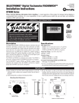
1
UM-17473-G DT9800 Series User’s Manual Seventh Edition March, 2002 Copyright © 1999, 2000, 2002 by Data Translation, Inc. All rights reserved. No part of this publication may be reproduced, stored in a retrieval system, or transmitted, in any form by any means, electronic, mechanical, by photocopying, recording, or otherwise, without the prior written permission of Data Translation, Inc. Information furnished by Data Translation, Inc. is believed to be accurate and reliable; however, no responsibility is assumed by Data Translation, Inc. for its use; nor for any infringements of patents or other rights of third parties which may result from its use. No license is granted by implication or otherwise under any patent rights of Data Translation, Inc. Use, duplication, or disclosure by the United States Government is subject to restrictions as set forth in subparagraph (c)(1)(ii) of the Rights in Technical Data and Computer software clause at 48 C.F.R, 252.227-7013, or in subparagraph (c)(2) of the Commercial computer Software Registered Rights clause at 48 C.F.R., 52-227-19 as applicable. Data Translation, Inc., 100 Locke Drive, Marlboro, MA 01752 Data Translation, Inc. 100 Locke Drive Marlboro, MA 01752-1192 (508) 481-3700 www.datatranslation.com Fax: (508) 481-8620 E-mail: [email protected] Data Translation® is a registered trademark of Data Translation, Inc. DT-Open LayersTM, DataAcq SDKTM , DataAcq OMNI CDTM, DT-LV LinkTM, DTx-EZTM , and DT VPITM are trademarks of Data Translation, Inc. All other brand and product names are trademarks or registered trademarks of their respective companies. Radio and Television Interference This equipment has been tested and found to comply with CISPR EN55022 Class A, and EN50082-1 (CE) requirements and also with the limits for a Class A digital device, pursuant to Part 15 of the FCC Rules. These limits are designed to provide reasonable protection against harmful interference when the equipment is operated in a commercial environment. This equipment generates, uses, and can radiate radio frequency energy and, if not installed and used in accordance with the instruction manual, may cause harmful interference to radio communications. Operation of this equipment in a residential area is likely to cause harmful interference, in which case the user will be required to correct the interference at his own expense. Changes or modifications to this equipment not expressly approved by Data Translation could void your authority to operate the equipment under Part 15 of the FCC Rules. Note: This product was verified to meet FCC requirements under test conditions that included use of shielded cables and connectors between system components. It is important that you use shielded cables and connectors to reduce the possibility of causing interference to radio, television, and other electronic devices. Canadian Department of Communications Statement This digital apparatus does not exceed the Class A limits for radio noise emissions from digital apparatus set out in the Radio Interference Regulations of the Canadian Department of Communications. Le présent appareil numérique n’émet pas de bruits radioélectriques dépassant les limites applicables aux appareils numériques de la class A prescrites dans le Règlement sur le brouillage radioélectrique édicté par le Ministère des Communications du Canada. Table of Contents About this Manual . . . . . . . . . . . . . . . . . . . . . . . . . . . . . . . . . . ix Intended Audience. . . . . . . . . . . . . . . . . . . . . . . . . . . . . . . . . . . . . . ix What You Should Learn from this Manual. . . . . . . . . . . . . . . . . . ix Conventions Used in this Manual . . . . . . . . . . . . . . . . . . . . . . . . . . x Related Information . . . . . . . . . . . . . . . . . . . . . . . . . . . . . . . . . . . . . xi Where To Get Help. . . . . . . . . . . . . . . . . . . . . . . . . . . . . . . . . . . . . . xii Chapter 1: Overview . . . . . . . . . . . . . . . . . . . . . . . . . . . . . . . . 1 Features . . . . . . . . . . . . . . . . . . . . . . . . . . . . . . . . . . . . . . . . . . . . . . . . 2 Supported Software . . . . . . . . . . . . . . . . . . . . . . . . . . . . . . . . . . . . . . 7 Accessories . . . . . . . . . . . . . . . . . . . . . . . . . . . . . . . . . . . . . . . . . . . . . 9 Chapter 2: Principles of Operation . . . . . . . . . . . . . . . . . . . 11 Analog Input Features . . . . . . . . . . . . . . . . . . . . . . . . . . . . . . . . . . . 13 Input Resolution . . . . . . . . . . . . . . . . . . . . . . . . . . . . . . . . . . . . 13 Analog Input Channels . . . . . . . . . . . . . . . . . . . . . . . . . . . . . . 14 Specifying a Single Channel . . . . . . . . . . . . . . . . . . . . . . 15 Specifying One or More Channels . . . . . . . . . . . . . . . . . 16 Specifying Digital Input Lines in the Analog Input Channel List . . . . . . . . . . . . . . . . . . . . . . . . . . . . . . . . . . . . 16 Performing Dynamic Digital Output Operations . . . . 17 Input Ranges and Gains. . . . . . . . . . . . . . . . . . . . . . . . . . . . . . 19 Specifying the Gain for a Single Channel . . . . . . . . . . . 22 Specifying the Gain for One or More Channels . . . . . . 22 A/D Sample Clock Sources . . . . . . . . . . . . . . . . . . . . . . . . . . . 23 Internal A/D Sample Clock . . . . . . . . . . . . . . . . . . . . . . . 23 External A/D Sample Clock . . . . . . . . . . . . . . . . . . . . . . 25 Triggers . . . . . . . . . . . . . . . . . . . . . . . . . . . . . . . . . . . . . . . . . . . . 25 v Contents Analog Input Conversion Modes . . . . . . . . . . . . . . . . . . . . . . 26 Continuously Paced Scan Mode . . . . . . . . . . . . . . . . . . . 27 Triggered Scan Mode . . . . . . . . . . . . . . . . . . . . . . . . . . . . 28 Internally Retriggered Scan Mode . . . . . . . . . . . . . . 28 Externally Retriggered Scan Mode. . . . . . . . . . . . . . 31 Data Format . . . . . . . . . . . . . . . . . . . . . . . . . . . . . . . . . . . . . . . . 33 Data Transfer . . . . . . . . . . . . . . . . . . . . . . . . . . . . . . . . . . . . . . . 36 Error Conditions . . . . . . . . . . . . . . . . . . . . . . . . . . . . . . . . . . . . 37 Analog Output Features . . . . . . . . . . . . . . . . . . . . . . . . . . . . . . . . . 39 Output Resolution. . . . . . . . . . . . . . . . . . . . . . . . . . . . . . . . . . . 39 Analog Output Channels . . . . . . . . . . . . . . . . . . . . . . . . . . . . . 40 Output Ranges and Gains . . . . . . . . . . . . . . . . . . . . . . . . . . . . 41 Conversion Modes . . . . . . . . . . . . . . . . . . . . . . . . . . . . . . . . . . 42 Data Format . . . . . . . . . . . . . . . . . . . . . . . . . . . . . . . . . . . . . . . . 42 Digital I/O Features . . . . . . . . . . . . . . . . . . . . . . . . . . . . . . . . . . . . . 44 Digital I/O Lines . . . . . . . . . . . . . . . . . . . . . . . . . . . . . . . . . . . . 44 Resolution. . . . . . . . . . . . . . . . . . . . . . . . . . . . . . . . . . . . . . . . . . 45 Operation Modes. . . . . . . . . . . . . . . . . . . . . . . . . . . . . . . . . . . . 45 Counter/Timer Features . . . . . . . . . . . . . . . . . . . . . . . . . . . . . . . . . 46 Units . . . . . . . . . . . . . . . . . . . . . . . . . . . . . . . . . . . . . . . . . . . . . . 46 C/T Clock Sources . . . . . . . . . . . . . . . . . . . . . . . . . . . . . . . . . . 47 Internal C/T Clock . . . . . . . . . . . . . . . . . . . . . . . . . . . . . . 47 External C/T Clock . . . . . . . . . . . . . . . . . . . . . . . . . . . . . . 47 Internally Cascaded Clock . . . . . . . . . . . . . . . . . . . . . . . . 48 Gate Types . . . . . . . . . . . . . . . . . . . . . . . . . . . . . . . . . . . . . . . . . 49 Pulse Output Types and Duty Cycles . . . . . . . . . . . . . . . . . . 51 Counter/Timer Operation Modes . . . . . . . . . . . . . . . . . . . . . 53 Event Counting . . . . . . . . . . . . . . . . . . . . . . . . . . . . . . . . . 53 Frequency Measurement . . . . . . . . . . . . . . . . . . . . . . . . . 54 Rate Generation . . . . . . . . . . . . . . . . . . . . . . . . . . . . . . . . . 56 vi Contents One-Shot . . . . . . . . . . . . . . . . . . . . . . . . . . . . . . . . . . . . . . . 59 Repetitive One-Shot . . . . . . . . . . . . . . . . . . . . . . . . . . . . . 61 Chapter 3: Supported Device Driver Capabilities. . . . . . . . 65 Chapter 4: Programming Flowcharts. . . . . . . . . . . . . . . . . . 77 Single-Value Operations . . . . . . . . . . . . . . . . . . . . . . . . . . . . . . . . . 79 Continuous A/D Operations . . . . . . . . . . . . . . . . . . . . . . . . . . . . . 81 Event Counting Operations . . . . . . . . . . . . . . . . . . . . . . . . . . . . . . 83 Frequency Measurement Operations . . . . . . . . . . . . . . . . . . . . . . 85 Pulse Output Operations. . . . . . . . . . . . . . . . . . . . . . . . . . . . . . . . . 87 Chapter 5: Calibration . . . . . . . . . . . . . . . . . . . . . . . . . . . . . 101 Running the Calibration Utility . . . . . . . . . . . . . . . . . . . . . . . . . . 103 Calibrating the Analog Input Subsystem . . . . . . . . . . . . . . . . . . 104 Configuring for Calibration . . . . . . . . . . . . . . . . . . . . . . . . . . 104 Calibrating the Analog Input Circuitry . . . . . . . . . . . . . . . . 105 Using the Auto-Calibration Procedure . . . . . . . . . . . . 105 Using the Manual Calibration Procedure . . . . . . . . . . 106 Calibrating the Thermocouple Circuitry . . . . . . . . . . . . . . . 107 Calibrating the Analog Output Subsystem . . . . . . . . . . . . . 109 Chapter 6: Troubleshooting . . . . . . . . . . . . . . . . . . . . . . . . 111 General Checklist . . . . . . . . . . . . . . . . . . . . . . . . . . . . . . . . . . . . . . 112 Service and Support . . . . . . . . . . . . . . . . . . . . . . . . . . . . . . . . . . . . 115 Telephone Technical Support. . . . . . . . . . . . . . . . . . . . . . . . . 115 E-Mail and Fax Support . . . . . . . . . . . . . . . . . . . . . . . . . . . . . 118 World-Wide Web . . . . . . . . . . . . . . . . . . . . . . . . . . . . . . . . . . . 118 If Your Board Needs Factory Service. . . . . . . . . . . . . . . . . . . . . . 119 vii Contents Appendix A: Specifications . . . . . . . . . . . . . . . . . . . . . . . . 121 Appendix B: Connector Pin Assignments . . . . . . . . . . . . 133 Index . . . . . . . . . . . . . . . . . . . . . . . . . . . . . . . . . . . . . . . . . . . . 141 viii About this Manual This manual describes the features of the DT9800 Series function modules, the capabilities of the DT9800 Series Device Driver, and how to program the DT9800 Series function modules using DT-Open Layers software. Calibration and troubleshooting information is also provided. Intended Audience This document is intended for engineers, scientists, technicians, or others responsible for using and/or programming the DT9800 Series function modules for data acquisition operations in Microsoft® Windows® 98, Windows Me (Millennium Edition), Windows 2000, Windows XP, or the Macintosh® (MAC OS 9.0) operating system. It is assumed that you have some familiarity with data acquisition principles and that you understand your application. What You Should Learn from this Manual This manual provides detailed information about the features of the DT9800 Series function modules and the capabilities of the DT9800 Series Device Driver. The manual is organized as follows: • Chapter 1, “Overview,” describes the major features of the modules, as well as the supported software and accessories for the modules. • Chapter 2, “Principles of Operation,” describes all of the features of the modules and how to use them in your application. • Chapter 3, “Supported Device Driver Capabilities,” lists the data acquisition subsystems and the associated features accessible using the DT9800 Series Device Driver. ix About this Manual • Chapter 4, “Programming Flowcharts,” describes the processes you must follow to program the subsystems on the DT9800 Series module using DT-Open Layers-compliant software. • Chapter 5, “Calibration,” describes how to calibrate the analog I/O circuitry of the modules. • Chapter 6, “Troubleshooting,” provides information that you can use to resolve problems with the modules and the device driver, should they occur. • Appendix A, “Specifications,” lists the specifications of the modules. • Appendix B, “Connector Pin Assignments,” shows the pin assignments for the connectors and the screw terminal assignments for the modules. • An index completes this manual. Conventions Used in this Manual The following conventions are used in this manual: • Notes provide useful information or information that requires special emphasis, cautions provide information to help you avoid losing data or damaging your equipment, and warnings provide information to help you avoid catastrophic damage to yourself or your equipment. • Items that you select or type are shown in bold. x About this Manual Related Information Refer to the following documents for more information on using the DT9800 Series function modules: • Benefits of the Universal Serial Bus for Data Acquisition. This white paper describes why USB is an attractive alternative for data acquisition. It is available on the Data Translation web site (www.datatranslation.com). • DT9800 Series Getting Started Manual (UM-17471). This manual, included on the Data Acquisition OMNI CDTM, describes the how to install the DT9800 Series function modules and related software. • DT Measure Foundry Getting Started Manual (UM-19298) and online help. These documents describe how to use DT Measure Foundry™ to build drag-and-drop test and measurement applications for Data Translation® data acquisition devices without programming. • DataAcq SDK User’s Manual (UM-18326). For programmers who are developing their own application programs using the Microsoft C compiler, this manual describes how to use the DT-Open Layers DataAcq SDKTM to access the capabilities of Data Translation data acquisition devices. • DTx-EZ Getting Started Manual (UM-15428). This manual describes how to use the ActiveX controls provided in DTx-EZTM to access the capabilities of Data Translation data acquisition devices in Microsoft Visual Basic® or Visual C++®. • DT VPI User Manual (UM-16150). This manual describes how to use DT VPITM and the Agilent® VEE™ visual programming language to access the capabilities of Data Translation data acquisition devices. • DT-LV Link Getting Started Manual (UM-15790). This manual describes how to use DT-LV LinkTM with the LabVIEW® graphical programming language to access the capabilities of Data Translation data acquisition devices. xi About this Manual • Microsoft Windows 98, Windows Me, Windows 2000, Windows XP, or Macintosh documentation. • USB web site (http://www.usb.org). • Omega Complete Temperature Measurement Handbook and Encyclopedia®. This document, published by Omega Engineering, provides information on how to linearize voltage values into temperature readings for various thermocouple types. Where To Get Help Should you run into problems installing or using a DT9800 Series function module, the Data Translation Technical Support Department is available to provide technical assistance. Refer to Chapter 6 for more information. If you are outside the United States or Canada, call your local distributor, whose number is listed in your Data Translation product handbook. xii 1 Overview Features . . . . . . . . . . . . . . . . . . . . . . . . . . . . . . . . . . . . . . . . . . . . . . . . 2 Supported Software . . . . . . . . . . . . . . . . . . . . . . . . . . . . . . . . . . . . . . 7 Accessories . . . . . . . . . . . . . . . . . . . . . . . . . . . . . . . . . . . . . . . . . . . . . 9 1 Chapter 1 Features The DT9800 Series is a family of low-cost, multifunction data acquisition modules for the Universal Serial Bus (USB). USB is a new standard for connecting PCs to peripheral devices, such as printers, mice, and modems, and was developed to make more low-cost ports available for the increasing number of these devices. Most new computers have two USB ports that allow direct connection to USB devices. You can expand the number of USB devices attached to a single USB port by using expansion hubs. DT9800 Series function modules are part of the high-power, bus-powered USB class; therefore, the modules do not require external power, but the expansion hubs do require external power. DT9800 Series function modules reside outside of the PC and install with a single cable to ease installation. Modules can be “hot swapped” or plugged and unplugged while the PC is on, making them useful for many data acquisition applications. The DT9800 Series includes the following subseries: DT9800 Standard Series, DT9800-MAC Series, DT9800-EC Series, and DT9800-EC-I Series. The DT9800-EC Series modules are not isolated; the DT9800 Standard Series, DT9800-MAC Series, and DT9800-EC-I Series modules are isolated. In addition, the DT9800-EC and DT9800-EC-I Series modules support the use of optional backplanes and screw terminal panels that provide signal conditioning and other features. Table 1 lists the function modules in each series and the key features of each. 2 Overview Table 1: Key Features Among the DT9800 Series Series DT9800 Standard Series Operating System Windows Function Modules # of Analog Inputs Analog Input Sample Rate # of Analog Outputs # of Digital I/O Lines 1 # of Counter /Timers a DT9801 16 SE/ 8 DI 100 kS/s 0 8 input, 8 output 2 DT9802a 16 SE/ 8 DI 100 kS/s 2 8 input, 8 output 2 DT9803b 16 SE/ 8 DI 100 kS/s 0 8 input, 8 output 2 DT9804b 16 SE/ 8 DI 100 kS/s 2 8 input, 8 output 2 DT9805c 16 SE/ 8 DI/ 7 thermocouples and 1 CJC 50 kS/s 0 8 input, 8 output 2 DT9806c 16 SE/ 8 DI/ 7 thermocouples and 1 CJC 50 kS/s 2 8 input, 8 output 2 1 1 1 1 1 1 1 1 3 Chapter 1 Table 1: Key Features Among the DT9800 Series (cont.) Series DT9800MAC Series DT9800EC Seriesd DT9800EC-I Seriesd # of Analog Outputs # of Digital I/O Lines Operating System Function Modules Macintosh DT9801MACa 16 SE/ 8 DI 100 kS/s 0 8 input, 8 output 2 DT9802MACa 16 SE/ 8 DI 100 kS/s 2 8 input, 8 output 2 DT9803MACb 16 SE/ 8 DI 100 kS/s 0 8 input, 8 output 2 DT9804MACb 16 SE/ 8 DI 100 kS/s 2 8 input, 8 output 2 DT9801-E Ca 16 SE/ 8 DIe 100 kS/s 0 8 input, 8 output 2 DT9802-E Ca 16 SE/ 8 DIe 100 kS/s 2f 8 input, 8 output 2 DT9803-E Cb 16 SE/ 8 DIg 100 kS/s 0 8 input, 8 output 2 DT9804-E Cb 16 SE/ 8 DIg 100 kS/s 2h 8 input, 8 output 2 DT9801-E C-Ia 16 SE/ 8 DIe 100 kS/s 0 8 input, 8 output 2 DT9802-E C-Ia 16 SE/ 8 DIe 100 kS/s 2f 8 input, 8 output 2 DT9803-E C-Ib 16 SE/ 8 DIg 100 kS/s 0 8 input, 8 output 2 DT9804-E C-I 16 SE/ 8 DIg 100 kS/s 2h 8 input, 8 output 2 Windows Windows a. The resolution is 12 bits. b. The resolution is 16 bits. 4 Analog Input Sample Rate # of Analog Inputs # of Counter /Timers Overview c. The gains provided on the DT9805 and DT9806 are 1, 10, 100, and 500. All other modules provide gains of 1, 2, 4, and 8. d. The DT9800-EC Series boards are nonisolated; the DT9800-EC-I Series boards and all other DT9800 Series boards are isolated. e. The analog input range is 0 to 10 V or ±10 V. f. The analog output range is 0 to 10 V, 0 to 5 V, ±10 V, or ±5 V. g. The analog input range is ±10 V. h. The analog output range is ±10 V. All DT9800 Series function modules share the following major features: • USB compatibility; • Software configurable termination resistance for differential inputs on a channel-by-channel basis. • Input gains of 1, 2, 4, and 8 for all modules except the DT9805 and DT9806, which support gains of 1, 10, 100, and 500; • Continuously paced and triggered scan capability; • A 32-location channel-gain list that supports sampling analog input channels at the same or different gains in sequential or random order; • Internal and external clock sources for the analog input subsystem; 1 1 1 1 1 1 • Digital TTL triggering for the analog input subsystem; • One 8-bit digital input port and one 8-bit digital output port; the digital input lines can be included as part of the analog input channel-gain list to correlate the timing of analog and digital events; digital outputs can drive external solid-state relays; and • One dynamic digital output line; • Two 16-bit user counter/timers programmable for event counting, frequency measurement, rate generation (continuous pulse output), one-shot, and repetitive-one shot pulse output operations. 1 1 1 • Programmable gate types and pulse output types. 5 Chapter 1 In addition, the DT9805 and DT9806 function modules provide thermocouples and low-level analog input capability. The DT9800 Standard, DT9800-EC, and DT9800-EC-I Series modules also provide software calibration for the analog I/O subsystems. 6 Overview Supported Software The following software is available for use with the DT9800 Series modules: • DT9800 Series Device Driver − This software is provided on the Data Acquisition OMNI CDTM (for Windows 98, Windows Me, Windows 2000, and Windows XP) or the DT9800 Series CD-ROM for the Macintosh, and is shipped with the module. The device driver allows you to use a DT9800 Series function module with any of the supported software packages or utilities. Refer to the DT9800 Series Getting Started Manual (UM-17471) for more information on loading and configuring the device driver. 1 1 1 • Quick Data Acq application − This software is provided on the Data Acquisition OMNI CD (for Windows 98, Windows Me, Windows 2000, and Windows XP) or the DT9800 Series CD-ROM for the Macintosh, and is shipped with the module. The Quick Data Acq application provides a quick way to get up and running using a DT9800 Series function module. Using this application, you can verify key features of the modules, display data on the screen, and save data to disk. Refer to the DT9800 Series Getting Started Manual (UM-17471) for more information on using the Quick Data Acq application. 1 • Scope application − This software is shipped with the board on the Data Acquisition OMNI CD. This application emulates three basic instruments: a simple oscilloscope chart recorder, a data logger, and a multi-channel oscilloscope. Using the Scope application, you can monitor data online and capture it to disk. Refer to the online documentation provided on the CD-ROM for more information. 1 • Calibration Utility − This software is provided on the Data Acquisition OMNI CD-ROM (for Windows 98, Windows Me, Windows 2000, and Windows XP). (Currently, this utility is not provided for the Macintosh.) The Calibration Utility allows you to calibrate the analog I/O circuitry of the function modules. Refer to Chapter 5 for more information on this utility. 1 1 1 1 7 Chapter 1 • DT Measure Foundry − An evaluation version of this software is included on the Data Acquisition OMNI CD. DT Measure Foundry is drag-and-drop test and measurement application builder designed to give you top performance with ease-of-use development. Order the full development version of this software package to develop your own application using real hardware. • DataAcq SDK − This software is shipped on the Data Acquisition OMNI CD. Use the Data Acq SDK if you want to use Windows 98, Windows Me, Windows NT 4.0, Windows 2000, or Windows XP to develop your own application software for the DT9800 Series boards using the Microsoft C compiler; the DataAcq SDK complies with the DT-Open Layers standard. • DTx-EZ − Order this optional software package if you want to use ActiveX controls to access the capabilities of the DT9800 Series boards using Microsoft Visual Basic or Visual C++; DTx-EZ complies with the DT-Open Layers standard. • DT VPI − Order this optional software package if you want to use the Aglient VEE visual programming language to access the capabilities of the DT9800 Series boards. • DT-LV Link − Order this optional software package if you want to use the LabVIEW graphical programming language to access the capabilities of the DT9800 Series boards. • Testpoint − Order this optional software package if you want use a drag-and-drop software environment for designing test, measurement, and data acquisition applications. Refer to the Data Translation data acquisition catalog for information about selecting the right software package for your needs. 8 Overview Accessories One EP310 cable is shipped with each DT9800 Series function module. The EP310 is a 2-meter, USB cable that connects the USB connector of the DT9800 Series function module to the USB connector on the host computer. If you want to buy additional USB cables, EP310 is available as an accessory product for the DT9800 Series. In addition, you can purchase the following optional items from Data Translation for use with the DT9800 Series: • EP316 − a 5-meter, USB cable that connects the USB connector of the DT9800 Series function module to the USB connector on the host computer. • 5B01 − a 16-channel backplane that accepts 5B Series signal conditioning modules. • 5B08 − an 8-channel backplane that accepts 5B Series signal conditioning modules. • 7BP16-1 − a 16-channel backplane that accepts 7B Series signal conditioning modules. • 7BP08-1 − an 8-channel backplane that accepts 7B Series signal conditioning modules. • 7BP04-1 − a 4-channel backplane that accepts 7B Series signal conditioning modules. • AC1324 − a screw terminal panel that connects to a DT9800-EC or DT9800-EC-I Series function module to allow access to the analog I/O, dynamic digital output, counter/timer, and power signals. • PB16H − a digital backplane that connects to the DT9800-EC or DT9800-EC-I function module to allow access to the digital I/O signals. 1 1 1 1 1 1 1 1 1 9 Chapter 1 • STP-EZ − a screw terminal panel that connects to a DT9800-EC or DT9800-EC-I Series function module to allow access to the digital I/O signals. A 50-pin ribbon cable is provided with the STP-EZ to allow direct connection to a DT9800-EC or DT9800-EC-I Series function module. • AC1315 − a 2-foot, 26-pin female to 26-pin female cable that connects a 5B Series backplane to a DT9800-EC or DT9800-EC-I Series function module. • AC1393 − a 6-inch, 26-pin male to 25-pin female adapter cable that connects a 7B Series backplane to the AC1315 cable; the AC1315 cable then connects to a DT9800-EC or DT9800-EC-I Series function module. • EP035 − a 2.4-meter, 50-pin ribbon cable that connects the PB16H Opto 22 backplane to a DT9800-EC or DT9800-EC-I Series function module. 10 2 Principles of Operation Analog Input Features . . . . . . . . . . . . . . . . . . . . . . . . . . . . . . . . . . . 13 Analog Output Features . . . . . . . . . . . . . . . . . . . . . . . . . . . . . . . . . 39 Digital I/O Features . . . . . . . . . . . . . . . . . . . . . . . . . . . . . . . . . . . . . 44 Counter/Timer Features . . . . . . . . . . . . . . . . . . . . . . . . . . . . . . . . . 46 11 Chapter 2 Figure 1 shows a block diagram of the DT9800 Series function modules. Note that bold entries indicate signals you can access. +5 V D+ D− Ground USB Interface Isolated DC-DC and Power Control* MicroController 500 V Isolation Barrier * High-Speed Isolated Data Path *Note that this is not isolated on the DT9800-EC Series. Isolated Power* Dynamic Digital Out Clock Two 16-bit User Counter/Timers Gate Out Channel Gain List (32) Entries Isolated Side Control Logic* 8 Digital Outputs 16 SE/8 DI Analog Inputs Analog Input MUX 10 kΩ Bias Return Termination Resistors 8 Digital Inputs PGA (x 1, 2, 4, 8) External Clock and Trigger Logic Trigger 2048 Sample FIFO 12- or 16-Bit ADC 12-or 16-Bit D/A DAC0 DAC1 Clock Figure 1: Block Diagram of the DT9800 Series Function Modules 12 Principles of Operation Analog Input Features This section describes the features of the analog input (A/D) subsystem, including the following: • Input resolution, described on this page; • Analog input channels, described on this page; 2 2 • Input ranges and gains, described on page 19; • A/D sample clock sources, described on page 23; • Analog input conversion modes, described on page 26; 2 • Triggers, described on page 25; • Data formats, described on page 33; • Data transfer, described on page 36; and 2 • Error conditions, described on page 37. 2 Input Resolution Table 2 lists the input resolution of the DT9800 Series function modules. Note that the resolution is fixed; it cannot be programmed in software. 2 Table 2: Input Resolution Function Module Series DT9800 Standard Module Name 2 Input Resolution DT9801 DT9802 12 bit DT9803 DT9804 DT9805 DT9806 16 bit 2 2 13 Chapter 2 Table 2: Input Resolution (cont.) Function Module Series DT9800-MAC Series DT9800-EC Series DT9800-EC-I Series Module Name Input Resolution DT9801-MAC DT9802-MAC 12 bit DT9803-MAC DT9804-MAC 16 bit DT9801-EC DT9802-EC 12 bit DT9803-EC DT9804-EC 16 bit DT9801-EC-I DT9802-EC-I 12 bit DT9803-EC-I DT9804-EC-I 16 bit Analog Input Channels All DT9800 Series function modules support 16 single-ended or pseudo-differential analog input channels or eight differential analog input channels. In addition, the DT9805 and DT9806 function modules provide a cold junction compensation (CJC) circuit on channel 0 at 10 mV/° C. Using the CJC, you can connect seven thermocouple inputs (in differential mode) to the DT9805 or DT9806 module. You configure the channel type as single-ended or differential through software. Using software, you can also select whether to use 10 kΩ termination resistance between the low side of each differential channel and isolated analog ground. This feature is particularly useful with floating signal sources. Refer to the DT9800 Series Getting 14 Principles of Operation Started Manual for more information on wiring to inputs and configuring the driver to use bias return termination resistance. Note: For pseudo-differential inputs, specify single-ended in software; in this case, how you wire these signals determines the configuration. The DT9800-EC Series boards do not provide isolated analog ground. The DT9800 Series function modules can acquire data from a single analog input channel or from a group of analog input channels. Channels are numbered 0 to 15 for single-ended and pseudo-differential inputs, and 0 to 7 for differential inputs. The following subsections describe how to specify the channels. Specifying a Single Channel The simplest way to acquire data from a single channel is to specify the channel for a single-value analog input operation using software; refer to page 26 for more information on single-value operations. You can also specify a single channel using the analog input channel list, described in the next section. Note: If you want to perform a single-value digital input operation while the A/D subsystem is configured, specify channel 16 (which corresponds to the digital input port) in the A/D single-value operation. 2 2 2 2 2 2 2 2 2 15 Chapter 2 Specifying One or More Channels You can read data from one or more analog input channels using an analog input channel list. You can group the channels in the list sequentially (starting either with 0 or with any other analog input channel) or randomly. You can also specify a single channel or the same channel more than once in the list. Using software, specify the channels in the order you want to sample them. You can enter up to 32 entries in the channel list. The channels are read in order (using continuously paced scan mode or triggered scan mode) from the first entry to the last entry in the channel list. Refer to page 26 for more information on the supported conversion modes. Specifying Digital Input Lines in the Analog Input Channel List In addition to the analog input channels, the DT9800 Series function modules allow you to read eight digital input lines (Port A, lines 0 to 7) using the analog input channel list. This feature is particularly useful when you want to correlate the timing of analog and digital events. To read these eight digital input lines, specify channel 16 in the analog input channel list. You can enter channel 16 anywhere in the list and can enter it more than once, if desired. Note: If channel 16 is the only channel in the channel-gain list, the module can read this channel at the maximum A/D sampling rate. 16 Principles of Operation The digital channel is treated like any other channel in the analog input channel list; therefore, all the clocking, triggering, and conversion modes supported for analog input channels are supported for these digital input lines, if you specify them this way. Performing Dynamic Digital Output Operations Using software, you can enable a synchronous dynamic digital output operation for the A/D subsystem. This feature is particularly useful for synchronizing and controlling external equipment. One dynamic digital output line (0) is provided (screw terminal 46). This line is set to a value of 0 on power up; a reset does not affect the values of the dynamic digital output line. Note that this line is provided in addition to the other eight digital output lines; see page 44 for more information on the digital I/O features. You specify the value (0 or 1) to write from the dynamic digital output line using a digital channel list. A value of 0 indicates a low-level signal; a value of 1 indicates a high-level signal. The digital channel list corresponds to the analog input channel list. As each entry in the analog input channel list is read, the corresponding value you specified in the digital channel list is output to the dynamic digital output line. For example, assume that the analog input channel list contains channels 0, 1, 2, and 3; that dynamic digital output operations are enabled; and that the values in the digital channel list are 1, 0, 0, 1. Figure 2 shows this configuration. 2 2 2 2 2 2 2 2 2 17 Chapter 2 Analog Channel List Digital Channel List 0 1 1 1 0 0 2 0 0 3 1 1 Dynamic Digital Output Line 0 Figure 2: An Example Using Dynamic Digital Outputs As analog input channel 0 is read, a high-level signal is output to the dynamic digital output line. As analog input channels 1 and 2 are read, a low-level signal is output to the dynamic digital output line. As analog input channel 3 is read, a high-level signal is output to the dynamic digital output line. On power up, a value of 0 is written to the dynamic digital output line. 18 Principles of Operation Input Ranges and Gains Table 3 lists the supported gains and effective input range of each DT9800 Series function module. 2 Table 3: Effective Input Range Function Module Series DT9800 Standard Module Name DT9801 DT9802 DT9803 DT9804 DT9805 DT9806 Gain Unipolar Input Range 2 Bipolar Input Range 1 0 to 10 V ±10 V 2 0 to 5 V ±5 V 4 0 to 2.5 V ±2.5 V 8 0 to 1.25 V ±1.25 V 1 N/A ±10 V 2 N/A ±5 V 4 N/A ±2.5 V 8 N/A ±1.25 V 1 N/A ±10 V 10 N/A ±1 V 100 N/A ±0.10 V 500 N/A ±0.020 V 2 2 2 2 2 2 2 19 Chapter 2 Table 3: Effective Input Range (cont.) Function Module Series DT9800-MAC Series Module Name DT9801-MAC DT9802-MAC DT9803-MAC DT9804-MAC DT9800-EC Series DT9801-EC DT9802-EC DT9803-EC DT9804-EC 20 Gain Unipolar Input Range Bipolar Input Range 1 0 to 10 V ±10 V 2 0 to 5 V ±5 V 4 0 to 2.5 V ±2.5 V 8 0 to 1.25 V ±1.25 V 1 N/A ±10 V 2 N/A ±5 V 4 N/A ±2.5 V 8 N/A ±1.25 V 1 0 to 10 V ±10 V 2 0 to 5 V ±5 V 4 0 to 2.5 V ±2.5 V 8 0 to 1.25 V ±1.25 V 1 N/A ±10 V 2 N/A ±5 V 4 N/A ±2.5 V 8 N/A ±1.25 V Principles of Operation Table 3: Effective Input Range (cont.) Function Module Series DT9800-EC-I Series Module Name DT9801-EC-I DT9802-EC-I DT9803-EC-I DT9804-EC-I Gain Unipolar Input Range Bipolar Input Range 1 0 to 10 V ±10 V 2 0 to 5 V ±5 V 4 0 to 2.5 V ±2.5 V 8 0 to 1.25 V ±1.25 V 1 N/A ±10 V 2 N/A ±5 V 4 N/A ±2.5 V 8 N/A ±1.25 V Using software, specify 0 to 10 V for unipolar ranges or −10 V to +10 V for bipolar ranges. Note that you specify the range for the entire analog input subsystem, not the range per channel. For each channel, choose the gain that has the smallest effective range that includes the signal you want to measure. For example, if you are using a DT9803 and the range of your analog input signal is ±1.05V, specify a range of −10 V to +10 V for the module and use a gain of 8 for the channel; the effective input range for this channel is then ±1.25 V, which provides the best sampling accuracy for that channel. The way you specify gain depends on how you specified the channels, as described in the following subsections. 2 2 2 2 2 2 2 2 2 21 Chapter 2 Note: The DT9805 and DT9806 modules support autoranging for single-value operations, where the board determines the appropriate gain for your range rather than you having to specify it. Refer to page 26 for more information on using autoranging. Specifying the Gain for a Single Channel The simplest way to specify gain for a single channel is to specify the gain for a single-value analog input operation using software; refer to page 26 for more information on single-value operations. You can also specify the gain for a single channel using an analog input gain list, described in the next section. Specifying the Gain for One or More Channels For DT9800 Series function modules, you can specify the gain for one or more analog input channels using an analog input gain list. Using software, set up the gain list by specifying the gain for each entry in the channel list. (The two lists together are often referred to as the channel-gain list.) For example, assume the analog input channel list contains three entries: channels 5, 6, and 7; the gain list might look like this: 2, 4, 1, where a gain of 2 corresponds to channel 5, a gain of 4 corresponds to channel 6, and a gain of 1 corresponds to channel 7. Note: For analog input channel 16 (the eight digital input lines) in the channel list, specify a gain of 1 in the gain list. 22 Principles of Operation A/D Sample Clock Sources The DT9800 Series function modules allow you to use one of two clock sources for pacing analog input operations in continuous mode: • The internal A/D sample clock, which uses the 24-bit A/D Counter on the module, or 2 2 • An external A/D sample clock, which you can connect to the screw terminal panel. You use an A/D sample clock to pace the acquisition of each channel in the channel-gain list; this clock is also called the A/D pacer clock. Note: If you enter digital input channel 16 in the channel-gain list, the A/D sample clock (internal or external) also paces the acquisition of the eight digital input lines. 2 2 2 The following subsections describe the internal and external A/D sample clocks in more detail. Internal A/D Sample Clock The internal A/D sample clock uses a 12 MHz time base. Conversions start on the rising edge of the counter output; the output pulse is active low. Using software, specify the clock source as internal and the clock frequency at which to pace the operation. The minimum frequency supported is 0.75 Hz (0.75 Samples/s); the maximum frequency supported depends on the module type. Table 4 lists the maximum sampling rate of the DT9800 Series function modules. 2 2 2 2 23 Chapter 2 Table 4: Maximum Sampling Rate Function Module Series DT9800 Standard Module Name Sampling Rate DT9801 DT9802 DT9803 DT9804 100 kSamples/s DT9805a DT9806a 50 kSamples/s DT9800-MAC DT9801-MAC DT9802-MAC DT9803-MAC DT9804-MAC 100 kSamples/s DT9800-EC DT9801-EC DT9802-EC DT9803-EC DT9804-EC 100 kSamples/s DT9800-EC-I DT9801-EC-I DT9802-EC-I DT9803-EC-I DT9804-EC-I 100 kSamples/s a. The maximum rate is 50 kSamples/s for a single channel or a channel scan when the gain is 1 or 10, 10 kSamples/s for a channel scan when the gain is 100, and 2 kSamples/s for a channel scan when the gain is 500. According to sampling theory (Nyquist Theorem), specify a frequency that is at least twice as fast as the input’s highest frequency component. For example, to accurately sample a 20 kHz signal, specify a sampling frequency of at least 40 kHz. Doing so avoids an error condition called aliasing, in which high frequency input components erroneously appear as lower frequencies after sampling. 24 Principles of Operation External A/D Sample Clock An external A/D sample clock is useful when you want to pace acquisitions at rates not available with the internal A/D sample clock or when you want to pace at uneven intervals. Connect an external A/D sample clock to screw terminal TB25 on the DT9800 Series function module (pin 25 on connector J1). Conversions start on the rising edge of the external A/D sample clock input signal. Using software, specify the clock source as external. For DT9800 Series function modules, the clock frequency is always equal to the frequency of the external A/D sample clock input signal that you connect to the module through the screw terminal panel. 2 2 2 2 Triggers A trigger is an event that occurs based on a specified set of conditions. The DT9800 Series function module supports the following trigger sources: • Software trigger − A software trigger event occurs when you start the analog input operation (the computer issues a write to the module to begin conversions). Using software, specify the trigger source as a software trigger. • External trigger − An external digital trigger event occurs when the DT9800 Series module detects a rising edge on the Ext A/D Trigger input signal connected to screw terminal TB24 on the DT9800 Series module (pin 24 of connector J1). The trigger signal is TTL-compatible. Using software, specify the trigger source as a external digital trigger (external for DataAcq SDK users). 2 2 2 2 2 25 Chapter 2 Analog Input Conversion Modes DT9800 Series function modules support the following conversion modes: • Single-value operations are the simplest to use. Using software, you can either specify the range, gain, and analog input channel, or you can specify the range and analog input channel and have the software determine the best gain for the range (called autoranging). The board acquires the data from the specified channel and returns the data immediately. Data can be returned as both counts and voltage. For a single-value operation, you cannot specify a clock source, trigger source, scan mode, or buffer. Single-value operations stop automatically when finished; you cannot stop a single-value operation. • Scan mode takes full advantage of the capabilities of the DT9800 Series function modules. In a scan, you can specify a channel-gain list, clock source, trigger source, scan mode, buffer, and buffer wrap mode using software. Two scan modes are supported: continuously paced scan mode and triggered scan mode (often called burst mode). These modes are described in the following subsections. Using software, you can stop a scan by performing either an orderly stop or an abrupt stop. In an orderly stop, the module finishes acquiring the data, stops all subsequent acquisition, and transfers the acquired data to host memory; all subsequent triggers or retriggers are ignored. In an abrupt stop, the module stops acquiring samples immediately; the acquired data is not transferred to host memory, and all subsequent triggers or retriggers are ignored. 26 Principles of Operation Continuously Paced Scan Mode Use continuously paced scan mode if you want to accurately control the period between conversions of individual channels in a scan. When it detects an initial trigger, the module cycles through the channel-gain list, acquiring and converting the value for each entry in the list (this process is defined as the scan). The module then wraps to the start of the channel-gain list and repeats the process continuously until either the allocated buffers are filled or until you stop the operation. Refer to page 36 for more information on buffers. The conversion rate is determined by the frequency of the A/D sample clock; refer to page 23 for more information on the A/D sample clock. The sample rate, which is the rate at which a single entry in the channel-gain list is sampled, is determined by the frequency of the A/D sample clock divided by the number of entries in the channel-gain list. To select continuously paced scan mode, use software to specify the dataflow as continuous and to specify a trigger source to start the operation. Refer to page 25 for more information on the supported trigger sources. Figure 3 illustrates continuously paced scan mode using a channel-gain list with three entries: channel 0, channel 1, and channel 2. In this example, analog input data is acquired on each clock pulse of the A/D sample clock. When it reaches the end of the channel-gain list, the module wraps to the beginning of the channel-gain list and repeats this process. Data is acquired continuously. 2 2 2 2 2 2 2 2 2 27 Chapter 2 Chan 0 Chan 2 Chan 0 Chan 2 Chan 0 Chan 2 Chan 0 Chan 2 Chan 1 Chan 1 Chan 1 Chan 1 A/D Sample Clock Trigger event occurs Data acquired continuously Figure 3: Continuously Paced Scan Mode Triggered Scan Mode DT9800 Series function modules support two triggered scan modes: internally retriggered and externally retriggered. These modes are described in the following subsections. Internally Retriggered Scan Mode Use internally retriggered scan mode if you want to accurately control both the period between conversions of individual channels in a scan and the period between each scan. This mode is useful when synchronizing or controlling external equipment or when acquiring a buffer of data on each trigger or retrigger. When it detects an initial trigger (either a software trigger or an external trigger), the DT9800 Series function module scans the channel-gain list once, then waits for an internal retrigger to occur. When it detects an internal retrigger, the board scans the channel-gain list once again, then waits for another internal retrigger to occur. The process repeats continuously until either the allocated buffers are filled or until you stop the operation; refer to page 36 for more information on buffers. 28 Principles of Operation The sample rate is determined by the frequency of the A/D sample clock divided by the number of entries in the channel-gain list; refer to page 23 for more information on the A/D sample clock. The conversion rate of each scan is determined by the frequency of the internal retrigger clock. The internal retrigger clock is the Triggered Scan Counter on the board; the Triggered Scan Counter is a 24-bit counter with a 1 2MHz clock. Figure 4 illustrates triggered scan mode. In this example, post-trigger analog input data is acquired on each clock pulse of the A/D sample clock until the channel-gain list has been scanned once; then, the board waits for the retrigger event. When the retrigger event occurs, the board scans the channel-gain list once again, acquiring data on each pulse of the A/D sample clock. The process repeats continuously with every specified retrigger event. Chan 0 Chan 2 Chan 1 Chan 0 Chan 2 Chan 1 2 2 2 2 2 A/D Sample Clock 2 Trigger event occurs; data acquired for one scan of the CGL. Board waits for retrigger event. Retrigger event occurs; data acquired for one scan of the CGL. Figure 4: Triggered Scan Mode Specify the frequency of the internal retrigger clock using software. The minimum retrigger frequency is 0.75 Hz (0.75 Samples/s); the maximum retrigger rate of each DT9800 Series function module is listed in Table 5 on page 30. 2 2 2 29 Chapter 2 Table 5: Maximum Retrigger Frequency Function Module Series DT9800 Standard Module Name Maximum Retrigger Frequency DT9801 DT9802 DT9803 DT9804 100 kHz DT9805a DT9806a 50 kHz DT9800-MAC DT9801-MAC DT9802-MAC DT9803-MAC DT9804-MAC 100 kHz DT9800-EC DT9801-EC DT9802-EC DT9803-EC DT9804-EC 100 kHz DT9800-EC-I DT9801-EC-I DT9802-EC-I DT9803-EC-I DT9804-EC-I 100 kHz a. The maximum retrigger frequency is 50 kHz for a single channel or a channel scan when the gain is 1 or 10, 10 kHz for a channel scan when the gain is 100, and 2 kHz for a channel scan when the gain is 500. The appropriate retrigger frequency depends on a number of factors, determined by the following equations: + 2 µs Min. Retrigger = # of CGL entries Period A/D sample clock frequency 30 Principles of Operation Max. Retrigger = 1 Frequency Min. Retrigger Period For example, if you are using 16 channels in the channel-gain list, and using an A/D sample clock with a frequency of 50 kHz, set the maximum retrigger frequency to 3.106 kHz, since 3.106 kHz = 2 2 1 16 + 2 µs 50 kHz To select internally retriggered scan mode, use software to specify the following parameters: • The dataflow as continuous; • Triggered scan mode usage as enabled; 2 2 • The retrigger mode as internal; • The number of times to scan per trigger or retrigger (also called the multiscan count) as 1; 2 • The frequency of the retrigger clock; and • The initial trigger source; refer to page 25 for more information on the supported trigger sources. 2 Externally Retriggered Scan Mode Use externally retriggered scan mode if you want to accurately control the period between conversions of individual channels and retrigger the scan based on an external event. When a DT9800 Series function module detects an initial trigger (either a software trigger or an external trigger), the module scans the channel-gain list once, then waits for an external retrigger to occur. The external retrigger occurs when a rising edge is detected on the Ext A/D Trigger input screw terminal (TB24) on the module. 2 2 2 31 Chapter 2 When the retrigger occurs, the module scans the channel-gain list once, then waits for another external retrigger to occur. The process repeats continuously until either the allocated buffers are filled (if buffer wrap mode is none) or until you stop the operation (if buffer wrap mode is single or multiple); refer to page 36 for more information on buffers. The conversion rate of each channel is determined by the frequency of the A/D sample clock; refer to page 23 for more information on the A/D sample clock. The conversion rate of each scan is determined by the period between external retriggers; therefore, it cannot be accurately controlled. The module ignores external triggers that occur while it is acquiring data. Only external retrigger events that occur when the module is waiting for a retrigger are detected and acted on. To select externally retriggered scan mode, use software to specify the following parameters: • The dataflow as continuous; • The triggered scan mode usage as enabled; • The retrigger mode as an external retrigger (retrigger extra for DataAcq SDK users); • The number of times to scan per trigger or retrigger (also called the multiscan count) to 1; and • The retrigger source as the external trigger (external for DataAcq SDK users). Note: For DataAcq SDK users, if you want to use the same trigger source as both the initial trigger and the retrigger source, specify the external trigger as the initial trigger source and specify the retrigger mode as scan-per-trigger. In this case, you need not specify the retrigger source; the module uses the initial trigger source as the retrigger source. 32 Principles of Operation Data Format Table 6 lists the data encoding used by each DT9800 Series function module. 2 Table 6: Data Encoding Function Module Series DT9800 Standard Series DT9800-MAC DT9800-EC DT9800-EC-I Module Name 2 Data Encoding DT9801 DT9802 Straight Binary DT9803 DT9804 DT9805 DT9806 Offset Binary DT9801-MAC DT9802-MAC Straight Binary DT9803-MAC DT9804-MAC Offset Binary DT9801-EC DT9802-EC Straight Binary DT9803-EC DT9804-EC Offset Binary DT9801-EC-I DT9802-EC-I Straight Binary DT9803-EC-I DT9804-EC-I Offset Binary 2 2 2 2 2 2 2 33 Chapter 2 In software, the analog input value is returned as a code. To convert the code to voltage, use the following formulas: LSB = FSR 2N Vin = Code * LSB + Offset where, • LSB is the least significant bit. • FSR is the full-scale range. For the DT9800 Series, the full-scale range is 10 for the unipolar range or 20 for the bipolar range. • N is the input resolution. Refer to Table 2 on page 13 for the list of input resolutions supported. • Vin is the analog voltage. • Code is the raw count used by the software to represent the voltage. • Offset is the actual minus full-scale value. The minus full-scale value is 0.0 V for the unipolar input range and −10 V for the bipolar input range. For example, assume that you are using a DT9801 with a unipolar input range. If the software returns a code of 2010 for the analog input operation, determine the analog input voltage as follows: LSB = 10 4096 = 0.002441 V + 0.0 V Vin = 2010 * 0.002441 + 0 V Vin = 4.906 V 34 Principles of Operation Similarly, assume that you are using a DT9804 board with a bipolar input range. The actual minus full-scale value is −10.0 V. If the software returns a code of 2010 for the analog input operation, determine the analog input voltage as follows: LSB = 20 65536 = 0.000305 V 2 2 Vin = 2010 * 0.000305 + −10.0 V 2 Vin = −9.370 V Table 7 lists the values that are returned when the DT9800 Series function module is overrange. 2 Table 7: Overrange SIgnal Values Function Module Series DT9800 Standard Series DT9800-MAC Series DT9800-EC Series Module Name Above-Range Signals Below-Range Signals DT9801 DT9802 FFFh (plus full-scale) 000h (minus full-scale) DT9803 DT9804 DT9805 DT9806 FFFFh (plus full-scale) 0000h (minus full-scale) DT9801-MAC DT9802-MAC FFFh (plus full-scale) 000h (minus full-scale) DT9803-MAC DT9804-MAC FFFFh (plus full-scale) 0000h (minus full-scale) DT9801-EC DT9802-EC FFFh (plus full-scale) 000h (minus full-scale) DT9803-EC DT9804-EC FFFFh (plus full-scale) 0000h (minus full-scale) 2 2 2 2 2 35 Chapter 2 Table 7: Overrange SIgnal Values (cont.) Function Module Series DT9800-EC-I Series Module Name Above-Range Signals Below-Range Signals DT9801-EC-I DT9802-EC-I FFFh (plus full-scale) 000h (minus full-scale) DT9803-EC-I DT9804-EC-I FFFFh (plus full-scale) 0000h (minus full-scale) Data Transfer The module packs two bytes into each transfer to the host computer. Even samples (corresponding to entries 0, 2, 4, and so on, in the channel-gain list) are packed into the low bytes; odd samples (corresponding to entries 1, 3, 5, and so on, in the channel-gain list) are packed into the high bytes. DT9800 Series function modules contain a 2048-sample FIFO. During a continuous analog input operation, the hardware interrupts the firmware on the module when the FIFO is half full. The module then transfers 2048 samples to a circular buffer, which is dedicated to the hardware, in the host computer. The DT9800 Series Device Driver accesses the hardware circular buffer to fill user buffers that you allocate in software. Keep the following recommendations in mind when allocating user buffers for continuous analog input operations on the DT9800 Series: • Allocate a minimum of three user buffers. • Specify a buffer size at least as large as the sampling rate; for example, if you are using a sampling rate of 100 kSamples/s (100 kHz), specify a buffer size of 100,000. The minimum buffer size that you should specify is 256 samples. 36 Principles of Operation Note: If you are using a slow clock data rate, such as .75 Hz, and a 256 sample user buffer, you will have to wait over 5 minutes for any data since data is transferred only when 256 samples have been read. 2 2 • Specify one of the following buffer wrap modes: − If the wrap mode is none, data is written to the allocated buffers until no more empty buffers are available; at that point, the operation stops. − If wrap mode is multiple, data is written to the allocated multiple buffers continuously; when no more empty buffers are available, the module overwrites the data in the filled buffers starting with the first location of the first buffer. This process continues indefinitely until you stop it. − If wrap mode is single, data is written to a single buffer continuously; when the buffer is filled, the module overwrites the data in the buffer starting with the first location of the buffer. This process continues indefinitely until you stop it. Error Conditions The DT9800 Series function modules can report an error if one of the following conditions occurs: • A/D Over Sample error − The A/D sample clock rate is too fast. This error is reported if a new A/D sample clock pulse occurs while the ADC is busy performing a conversion from the previous A/D sample clock pulse. The host computer can clear this error. 2 2 2 2 2 2 To avoid this error, use a slower sampling rate. 2 37 Chapter 2 • A/D FIFO Full Flag set to 1 − The data was not read fast enough by the host computer. The host computer can clear this error. To avoid this error, ensure that you allocated at least three buffers, each at least as large as the sampling rate; for example, if you are using a sampling rate of 100 kSamples/s (100 kHz), specify a buffer size of 100,000 samples for each buffer. If one of these error conditions occurs, the module reports the error but continues to acquire and transfer data to the host computer. Note: The LED on the front panel will not blink green if the hardware detects an error. 38 Principles of Operation Analog Output Features An analog output (D/A) subsystem is provided on the following DT9800 Series function modules only: DT9802, DT9802-MAC, DT9802-EC, DT9802-EC-I, DT9804, DT9804-MAC, DT9804-EC, DT9804-EC-I, and DT9806. This section describes the following features of the D/A subsystem: 2 2 • Output resolution, described on this page; • Analog output channels, described on this page; • Output ranges and gains, described on page 41; 2 • Conversion modes, described on page 42; and 2 • Data format, described on page 42. Output Resolution Table 2 lists the output resolution of the DT9800 Series function modules. Note that the resolution is fixed; it cannot be programmed in software. 2 Table 8: Output Resolution Function Module Series Module Name 2 Resolution DT9800 Standard Series DT9802 12 bit DT9804 DT9806 16 bit DT9800-MAC Series DT9802-MAC 12 bit DT9804-MAC 16 bit 2 2 2 39 Chapter 2 Table 8: Output Resolution (cont.) Function Module Series DT9800-EC Series DT9800-EC-I Series Module Name Resolution DT9802-EC 12 bit DT9804-EC 16 bit DT9802-EC-I 12 bit DT9804-EC-I 16 bit Analog Output Channels The DT9802, DT9802-MAC, DT9802-EC, DT9802-EC-I, DT9804, DT9804-MAC, DT9804-EC, DT9804-EC-I, and DT9806 modules support two DC-level analog output channels (DAC0 and DAC1). Refer to the DT9800 Series Getting Started Manual for information on how to wire analog output signals to the module using the screw terminal panel. You configure the channel type through software. Within each DAC, the digital data is double-buffered to prevent spurious outputs, then output as an analog signal. Both DACs power up to a value of 0 V ±10 mV. Resetting the module does not clear the values in the DACs. The DT9800 Series function modules can output data from a single analog output channel only. Specify the channel for a single-value analog output operation using software; refer to “Conversion Modes,” on page 42 for more information on single-value operations. 40 Principles of Operation Output Ranges and Gains Table 9 lists the output range for each DT9800 Series function module. Table 9: Output Range Function Module Series DT9800 Standard Series DT9800-MAC Series DT9800-EC Series DT9800-EC-I Series Module Name Unipolar Output Range Bipolar Input Range DT9802 0 to 10 V or 0 to 5 V ±10 V or ±5 V DT9804 DT9806 N/A ±10 V DT9802-MAC 0 to 10 V or 0 to 5 V ±10 V or ±5 V DT9804-MAC N/A ±10 V DT9802-EC 0 to 10 V or 0 to 5 V ±10 V or ±5 V DT9804-EC N/A ±10 V DT9802-EC-I 0 to 10 V or 0 to 5 V ±10 V or ±5 V DT9804-EC-I N/A ±10 V 2 2 2 2 2 2 2 Specify the range using software; set the gain to 1. 2 2 41 Chapter 2 Conversion Modes DT9802, DT9802-MAC, DT9802-EC, DT9802-EC-I, DT9804, DT9804-MAC, DT9804-EC, DT9804-EC-I, and DT9806 modules can perform single-value analog output operations only. Use software to specify the range, gain, and analog output channel, then output the data from the specified channel. You cannot specify a clock source, trigger source, or buffer. Note: You cannot perform a single-value analog output operation while the A/D subsystem is running. The settling time for each DAC is 50 µs (20 V steps). Single-value operations stop automatically when finished; you cannot stop a single-value operation. Data Format Data from the host computer must use offset binary data encoding for analog output signals. Using software, specify the data encoding as binary. In software, you need to supply a code that corresponds to the analog output value you want the module to output. To convert a voltage to a code, use the following formulas: LSB = FSR 2N Code = Vout - offset LSB 42 Principles of Operation where, • LSB is the least significant bit. 2 • FSR is the full-scale range (10). • N is the output resolution; see Table 8 on page 39 for a list of output resolutions. 2 • Code is the raw count used by the software to represent the voltage. • Vout is the analog voltage. • Offset is the minus full-scale value, or −10 V. For example, assume that you are using a DT9804 module. If you want to output a voltage of 4.7 V, determine the code value as follows: LSB = 10 V 65536 = 0.0001526 V 2 2 2 Code = 4.7 V - (-10 V) 0.0001526 V Code = 96330 = 1784Ah 2 2 2 2 43 Chapter 2 Digital I/O Features This section describes the following features of the digital I/O subsystem: • Digital I/O lines, described on this page; • Resolution, described on this page; and • Operation modes, described on page 45. Digital I/O Lines DT9800 Series function modules support eight digital input lines (Port A, lines 0 to 7) through the DIN subsystem and eight digital output lines (Port B, lines 0 to 7) through the DOUT subsystem. For fast, clocked digital input operations, you can enter the digital input lines from Port A as channel 16 in the analog input channel list; refer to page 16 for more information. The DT9800 Series function modules also provide a dynamic digital output line that you can update when an analog input channel is read. Note that the dynamic digital output line is in addition to the digital output lines in Port B. Refer to page 17 for more information on dynamic digital output operations. On power up or module reset, no digital data is output from the modules. All the outputs include diode protection to the isolated ground and the isolated +5 V. Note: DT9800-EC Series function modules do not provide isolated ground or isolated +5 V power. 44 Principles of Operation Resolution The resolution of the digital input port is fixed at 8 bits; the resolution of the digital output port is also fixed at 8 bits. You cannot program the digital I/O resolution in software. 2 2 Operation Modes The DT9800 Series function modules support the following digital I/O operation modes: • Single-value operations are the simplest to use but offer the least flexibility and efficiency. You use software to specify the digital I/O port and a gain of 1 (the gain is ignored). Data is then read from or written to the digital I/O lines. For a single-value operation, you cannot specify a clock or trigger source. Single-value operations stop automatically when finished; you cannot stop a single-value operation. • Continuous digital input takes full advantage of the capabilities of the DT9800 Series function modules. In this mode, enter all eight digital input lines of Port A as channel 16 of the analog input channel-gain list; program this mode through the A/D subsystem. Using this mode, you can specify a clock source, scan mode, trigger source, buffer, and buffer wrap mode for the digital input operation. Refer to page 16 for more information on specifying digital input lines for a continuous digital input operation. • Dynamic digital output is useful for synchronizing and controlling external equipment and allows you to output data to the dynamic digital output line each time an analog input value is acquired. This mode is programmed through the A/D subsystem; refer to page 17 for more information. 2 2 2 2 2 2 2 45 Chapter 2 Counter/Timer Features The counter/timer circuitry on the module provides the clocking circuitry used by the A/D and D/A subsystems as well as several user counter/timer features. This section describes the following user counter/timer features: • Units, described on this page; • C/T clock sources, described on page 47; • Gate types, described on page 49; • Pulse types and duty cycles, described on page 51; and • Counter/timer operation modes, described on page 53. Units Two 16-bit counter/timers are supported by all DT9800 Series modules. The counters are numbered 0 and 1. Each counter accepts a clock input signal and gate input signal and outputs a clock output signal (also called a pulse output signal), as shown in Figure 5. Clock Input SIgnal (internal, external, or internally cascaded) Counter Gate Input Signal (software or external input) Figure 5: Counter/Timer Channel 46 Pulse Output Signal Principles of Operation Each counter corresponds to a counter/timer (C/T) subsystem. To specify the counter to use in software, specify the appropriate C/T subsystem. Counter 0 corresponds to C/T subsystem element 0; counter 1 corresponds to C/T subsystem element 1. C/T Clock Sources 2 2 The following clock sources are available for the user counters: • Internal C/T clock, • External C/T clock, and 2 • Internally cascaded clock. Refer to the following subsections for more information on these clock sources. Internal C/T Clock 2 2 The internal C/T clock uses a 12 MHz time base. Counter/timer operations start on the rising edge of the clock input signal. Through software, specify the clock source as internal and the frequency at which to pace the counter/timer operation (this is the frequency of the clock output signal). The maximum frequency that you can specify for the clock output signal is 750 kHz. The minimum frequency that you can specify for the clock output signal for each 16-bit counter is 183.1 Hz. The rising edge of the clock is the active edge. External C/T Clock An external C/T clock is useful when you want to pace counter/timer operations at rates not available with the internal C/T clock or if you want to pace at uneven intervals. The rising edge of the external C/T clock input signal is the active edge. 2 2 2 2 47 Chapter 2 Using software, specify the clock source as external and the clock divider used to determine the frequency at which to pace the operation. The minimum clock divider that you can specify is 2.0; the maximum clock divider that you can specify is 65,536. For example, if you supply an external C/T clock with a frequency of 700 kHz and specify a clock divider of 2, the resulting frequency of the external C/T clock output signal is 350 kHz. The resulting frequency of the external C/T clock output signal must not exceed 750 kHz. Table 10 on page 48 lists the screw terminals of the DT9800 Series modules that correspond to the external C/T clock signals of each counter/timer. Table 10: External C/T Clock Signals Module DT9800 Standard Series; DT9800-MAC Series DT9800-EC Series; DT9800-EC-I Series Counter /Timer Screw Terminal on Module J1 Pin Number Screw Terminal on AC1324 Panel J5 Pin Number 0 TB54 54 − − 1 TB50 50 − − 0 − − TB20 20 1 − − TB16 16 Internally Cascaded Clock You can also internally route the clock output signal from counter/timer 0 to the clock input signal of counter/timer 1 to internally cascade the counters. In this way, you can create a 32-bit counter without externally connecting two counters together. Specify internal cascade mode in software. The rising edge of the clock input signal is active. 48 Principles of Operation Through software, specify the clock source as internal and the frequency at which to pace the counter/timer operation (this is the frequency of the clock output signal). The maximum frequency that you can specify for the clock output signal is 750 kHz. For a 32-bit cascaded counter, the minimum frequency that you can specify for the clock output signal is 0.0028 Hz. 2 2 Gate Types The active edge or level of the gate input to the counter enables counter/timer operations. The operation starts when the clock input signal is received. Specify the gate type in software. DT9800 Series modules provide the following gate input types: • None − A software command enables any specified counter/timer operation immediately after execution. This gate type is useful for all counter/timer modes; refer to page 53 for more information on these modes. • Logic-low level external gate input − Enables a counter/timer operation when the external gate signal is low, and disables the counter/timer operation when the external gate signal is high. Note that this gate type is used only for event counting, frequency measurement, and rate generation; refer to page 53 for more information on these modes. • Logic-high level external gate input − Enables a counter/timer operation when the external gate signal is high, and disables a counter/timer operation when the external gate signal is low. Note that this gate type is used only for event counting, frequency measurement, and rate generation; refer to page 53 for more information on these modes. 2 2 2 2 2 2 2 49 Chapter 2 • Falling-edge external gate input − Enables a counter/timer operation on the transition from the high level to the low level (falling edge). In software, this is called a low-edge gate type. Note that this gate type is used only for one-shot and repetitive one-shot mode; refer to page 53 for more information on these modes. • Rising-edge external gate input − Enables a counter/timer operation on the transition from the low level to the high level (rising edge). In software, this is called a high-edge gate type. Note that this gate type is used only for one-shot and repetitive one-shot mode; refer to page 61 for more information on these modes. Table 11 lists the screw terminals and pin numbers on the DT9800 Series function modules that correspond to the gate input signals of each counter/timer. Table 11: Gate Input Signals Module DT9800 Standard Series; DT9800-MAC Series DT9800-EC Series; DT9800-EC-I Series 50 Counter /Timer Screw Terminal on Module J1 Pin Number Screw Terminal on AC1324 Panel J5 Pin Number 0 TB52 52 − − 1 TB48 48 − − 0 − − TB18 18 1 − − TB14 14 Principles of Operation Pulse Output Types and Duty Cycles DT9800 Series function modules can output pulses from each counter/timer. Table 12 lists the screw terminals of the modules that correspond to the pulse output signals of each counter/timer. 2 2 Table 12: Pulse Output Signals Module DT9800 Standard Series; DT9800-MAC Series DT9800-EC Series; DT9800-EC-I Series Counter /Timer Screw Terminal on Module J1 Pin Number Screw Terminal on AC1324 Panel J5 Pin Number 0 TB53 53 − − 1 TB49 49 − − 0 − − TB19 19 1 − − TB15 15 DT9800 Series function modules support the following pulse output types on the clock output signal: • High-to-low transitions − The low portion of the total pulse output period is the active portion of the counter/timer clock output signal. • Low-to-high transitions − The high portion of the total pulse output period is the active portion of the counter/timer pulse output signal. You specify the pulse output type in software. 2 2 2 2 2 2 2 51 Chapter 2 The duty cycle (or pulse width) indicates the percentage of the total pulse output period that is active. A duty cycle of 50, then, indicates that half of the total pulse is low and half of the total pulse output is high. You specify the duty cycle in software. Note: The minimum pulse width must be 650 ns. Figure 6 illustrates a low-to-high pulse with a duty cycle of approximately 30%. Active Pulse high pulse low pulse Total Pulse Period Figure 6: Example of a Low-to-High Pulse Output Type 52 Principles of Operation Counter/Timer Operation Modes DT9800 Series function modules support the following counter/timer operation modes: • Event counting, • Frequency measurement, 2 2 • Rate generation, • One-shot, and • Repetitive one-shot. 2 The following subsections describe these modes in more detail. Event Counting Use event counting mode to count events (clock pulses) from the counter’s associated clock input source. If you are using one counter, you can count a maximum of 65,536 events before the counter rolls over to 0 and starts counting again. If you are using a cascaded 32-bit counter, you can count a maximum of 4,294,967,296 events before the counter rolls over to 0 and starts counting again. In event counting mode, use an external C/T clock source; refer to page 47 for more information on the external C/T clock source. Using software, specify the counter/timer mode as event counting (count), the C/T clock source as external, and the gate type that enables the operation as logic high. Refer to page 51 for information on gates. Ensure that the signals are wired appropriately. Refer to the DT9800 Series Getting Started Manual for wiring examples. 2 2 2 2 2 2 53 Chapter 2 Figure 7 shows an example of an event counting operation using a logic-high gate type. high level enables operation Gate Input Signal External C/T Clock Input Signal low level disables operation 3 events are counted while the operation is enabled event counting operation starts event counting operation stops Figure 7: Example of Event Counting Frequency Measurement Use frequency measurement mode to measure the frequency of the signal from counter’s associated clock input source over a specified duration. In this mode, use an external C/T clock source; refer to page 47 for more information on the external C/T clock source. One way to perform a frequency measurement is to use the same wiring as an event counting application that does not use an external gate signal. Refer to the DT9800 Series Getting Started Manual for wiring examples. 54 Principles of Operation In this configuration, use software to specify the counter/timer mode as frequency measurement or event counting (count), and the duration of the system timer over which to measure the frequency. (The system timer uses a resolution of 1 ms.) In this configuration, frequency is determined using the following equation: Frequency Measurement = Number of Events Duration of the System Timer If you need more accuracy than the system timer provides, you can connect a pulse of a known duration (such as a one-shot output of another user counter) to the external gate input. Refer to the DT9800 Series Getting Started Manual for wiring examples. In this configuration, use software to set up the counter/timers as follows: 1. 2. 2 2 2 2 Set up one of the counter/timers for one-shot mode, specifying the clock source, clock frequency, gate type, type of output pulse (high or low), and duty cycle. 2 Set up the counter/timer that will measure the frequency for event counting mode, specifying the clock source to count, and the gate type (this should match the pulse output type of the counter/timer set up for one-shot mode). 2 3. Start both counters (events are not counted until the active period of the one-shot pulse is generated). 4. Read the number of events counted. (Allow enough time to ensure that the active period of the one-shot occurred and that events have been counted.) 5. Determine the measurement period using the following equation: Measurement period = * Active Pulse Width 1 Clock Frequency 2 2 2 55 Chapter 2 6. Determine the frequency of the clock input signal using the following equation: Frequency Measurement = Number of Events Measurement Period Figure 8 shows an example of a frequency measurement operation. In this example, three events are counted during a duration of 300 ms. The frequency, then, is 10 Hz, since 10 Hz = 3/(.3 s). 3 Events Counted External C/T Clock Input Signal Duration over which the frequency is measured = 300 ms frequency measurement starts frequency measurement stops Figure 8: Example of Frequency Measurement Rate Generation Use rate generation mode to generate a continuous pulse output signal from the counter; this mode is sometimes referred to as continuous pulse output or pulse train output. You can use this pulse output signal as an external clock to pace other operations, such as analog input or other counter/timer operations. While the pulse output operation is enabled, the counter outputs a pulse of the specified type and frequency continuously. As soon as the operation is disabled, rate generation stops. 56 Principles of Operation The period of the output pulse is determined by the clock input signal and the external clock divider. If you are using one counter (not cascaded), you can output pulses using a maximum frequency of 1 MHz (this is the frequency of the clock output signal). In rate generation mode, either the internal or external C/T clock input source is appropriate depending on your application; refer to page 47 for more information on the C/T clock source. Using software, specify the counter/timer mode as rate generation (rate), the C/T clock source as either internal or external, the polarity of the output pulses (high-to-low transitions or low-to-high transitions), the duty cycle of the output pulses, and the gate type that enables the operation as logic-high. Refer to page 51 for more information on pulse output signals and to page 49 for more information on gate types. Ensure that the signals are wired appropriately. Refer to the DT9800 Series Getting Started Manual for wiring examples. Figure 9 shows an example of an enabled rate generation operation using a logic-high gate input signal, an external C/T clock source with an input frequency of 4 kHz, a clock divider of 4, a low-to-high pulse type, and a duty cycle of 75%. A 1 kHz square wave is the generated output. Figure 10 shows the same example using a duty cycle of 25%. 2 2 2 2 2 2 2 2 2 57 Chapter 2 Rate Generation Operation Starts External C/T Clock Input Signal (4 kHz) Pulse Output Signal 75% duty cycle Figure 9: Example of Rate Generation Mode with a 75% Duty Cycle Continuous Pulse Output Operation Starts External C/T Clock Input Signal (4 kHz) Pulse Output Signal 25% duty cycle Figure 10: Example of Rate Generation Mode with a 25% Duty Cycle 58 Principles of Operation One-Shot 2 Use one-shot mode to generate a single pulse output signal from the counter when the operation is triggered (determined by the gate input signal). You can use this pulse output signal as an external digital (TTL) trigger to start other operations, such as analog input operations. 2 When the one-shot operation is triggered, a single pulse is output; then, the one-shot operation stops. All subsequent clock input signals and gate input signals are ignored. 2 The period of the output pulse is determined by the clock input signal. In one-shot mode, the internal C/T clock source is more useful than an external C/T clock source; refer to page 47 for more information on the internal C/T clock source. Using software, specify the counter/timer mode as one-shot, the clock source as internal, the polarity of the output pulse (high-to-low transition or low-to-high transition), the duty cycle of the output pulse, and the gate type to trigger the operation as rising edge. Refer to page 51 for more information on pulse output types and to page 49 for more information on gate types. Note: In the case of a one-shot operation, use a duty cycle as close to 100% as possible to output a pulse immediately. Using a duty cycle closer to 0% acts as a pulse output delay. Ensure that the signals are wired appropriately. Refer to the DT9800 Series Getting Started Manual for wiring examples. 2 2 2 2 2 2 59 Chapter 2 Figure 11 shows an example of a one-shot operation using an external gate input (rising edge), a clock output frequency of 1 kHz (pulse period of 1 ms), a low-to-high pulse type, and a duty cycle of 99.99%. Figure 12 shows the same example using a duty cycle of 50%. One-Shot Operation Starts External Gate Signal 1 ms period 99.99% duty cycle Pulse Output Signal Figure 11: Example of One-Shot Mode Using a 99.99% Duty Cycle 60 Principles of Operation 2 One-Shot Operation Starts 2 External Gate Signal 1 ms period Pulse Output Signal 2 2 50% duty cycle Figure 12: Example of One-Shot Mode Using a 50% Duty Cycle Repetitive One-Shot Use repetitive one-shot mode to generate a pulse output signal each time the module detects a trigger (determined by the gate input signal). You can use this mode to clean up a poor clock input signal by changing its pulse width, then outputting it. In repetitive one-shot mode, the internal C/T clock source is more useful than an external C/T clock source; refer to page 47 for more information on the internal C/T clock source. Use software to specify the counter/timer mode as repetitive one-shot (oneshot-rpt for SDK users), the polarity of the output pulses (high-to-low transitions or low-to-high transitions), the duty cycle of the output pulses, the C/T clock source, and the gate type to trigger the operation as rising edge. Refer to page 51 for more 2 2 2 2 2 61 Chapter 2 information on pulse output types and to page 49 for more information on gates. Note: In the case of a one-shot operation, use a duty cycle as close to 100% as possible to output a pulse immediately. Using a duty cycle closer to 0% acts as a pulse output delay. When the one-shot operation is triggered (determined by the gate input signal), a pulse is output. When the module detects the next trigger, another pulse is output. This operation continues until you stop the operation. Note: Triggers that occur while the pulse is being output are not detected by the module. Ensure that the signals are wired appropriately. Refer to the DT9800 Series Getting Started Manual for wiring examples. Figure 13 shows an example of a repetitive one-shot operation using an external gate (rising edge); a clock output frequency of 1 kHz (one pulse every 1 ms), a low-to-high pulse type, and a duty cycle of 99.99%. Figure 14 shows the same example using a duty cycle of 50%. 62 Principles of Operation 2 Repetitive One-Shot Operation Starts 2 External Gate Signal 1 ms period Pulse Output Signal 99.99% duty cycle 2 1 ms period 99.99% duty cycle 99.99% duty cycle 2 Figure 13: Example of Repetitive One-Shot Mode Using a 99.99% Duty Cycle 2 Repetitive One-Shot Operation Starts 2 External Gate Signal 2 1 ms period 1 ms period 2 Pulse Output Signal 50% duty cycle 50% duty cycle 2 Figure 14: Example of Repetitive One-Shot Mode Using a 50% Duty Cycle 63 Chapter 2 64 3 Supported Device Driver Capabilities 65 Chapter 3 The DT9800 Series Device Driver provides support for A/D, D/A, DIN, DOUT, and C/T subsystems. For information on how to configure the device driver, refer to the DT9800 Series Getting Started Manual. Table 13 summarizes the features available for use with the DataAcq SDK and the DT9800 Series function modules. The DataAcq SDK provides functions that return support information for specified subsystem capabilities at run-time. The first row in the table lists the subsystem types. The first column in the table lists all possible subsystem capabilities. A description of each capability is followed by the parameter used to describe that capability in the DataAcq SDK. Note: Blank fields represent unsupported options. The DataAcq SDK uses the functions olDaGetSSCaps (for those queries starting with OLSSC) and olDaGetSSCapsEx (for those queries starting with OLSSCE) to return the supported subsystem capabilities for a device. For more information, refer to the description of these functions in the DataAcq SDK online help. See the DataAcq User’s Manual for information on launching this help file. 66 Supported Device Driver Capabilities Table 13: DT9800 Series Supported Option s DT9800 Series A/D D/Aa DIN Total Subsystems on Module 1 1 1 Yes Yesb DOUT SRL 1 C/T 0 2 Single-Value Operation Support OLSSC_SUP_SINGLEVALUE Yes 3 3 Yes Continuous Operation Support OLSSC_SUP_CONTINUOUS Yes Continuous Operation until Trigger Event 3 Support OLSSC_SUP_CONTINUOUS_ Data Flow Mode Yes PRETRIG Continuous Operation before and after 3 Trigger Event OLSSC_SUP_CONTINUOUS_ ABOUTTRIG DT-Connect Support 3 OLSSC_SUP_DTCONNECT Continuous DT-Connect Support OLSSC_SUP_DTCONNECT_ CONTINUOUS 3 Burst DT-Connect Support Sim. Oper. Wind. Pause Simultaneous Start List Support Mess. Oper. OLSSC_SUP_DTCONNECT_BURST Pause Operation Support OLSSC_SUP_SIMULTANEOUS_START 3 OLSSC_SUP_PAUSE Asynchronous Operation Support OLSSC_SUP_POSTMESSAGE Yes 3 3 67 Chapter 3 Table 13: DT9800 Series Supported Options (cont.) DT9800 Series A/D D/Aa DIN Total Subsystems on Module 1 1 1 DOUT SRL 1 C/T 0 2 Buffer Support OLSSC_SUP_BUFFERING Yes Buffering Single Buffer Wrap Mode Support OLSSC_SUP_WRPSINGLE Yes Multiple Buffer Wrap Mode Support OLSSC_SUP_WRPMULTIPLE Yes Inprocess Buffer Flush Support OLSSC_SUP_INPROCESSFLUSH Yes Number of DMA Channels OLSSC_NUMDMACHANS 0 0 0 0 0 0 0 0 0 Supports Gap Free Data with No DMA DMA OLSSC_SUP_GAPFREE_NODMA Yes Supports Gap Free Data with Single DMA OLSSC_SUP_GAPFREE_SINGLEDMA Supports Gap Free Data with Dual DMA OLSSC_SUP_GAPFREE_DUALDMA Triggered Scan Support OLSSC_SUP_TRIGSCAN Yes Maximum Number of CGL Scans per Triggered Scan Mode Trigger OLSSC_MAXMULTISCAN 1 Supports Scan perTrigger Event Triggered Scan OLSSC_SUP_RETRIGGER_SCAN_ PER_TRIGGER Yes Supports Internal Retriggered Triggered Scan OLSSC_SUP_RETRIGGER_INTERNAL Yes Extra Retrigger Support OLSSC_SUP_RETRIGGER_EXTRA 68 Yes Supported Device Driver Capabilities (cont.) DT9800 Series A/D D/Aa DIN Total Subsystems on Module 1 1 1 Maximum Retrigger Frequency 100 kHz, OLSSCE_MAXRETRIGGER 50 kHzc DOUT SRL 1 C/T 0 OLSSCE_MINRETRIGGER 0 0 0 0 0.75 Hzd 0 0 0 0 32 0 0 0 Maximum Channel Gain List Depth OLSSC_CGLDEPTH 0 Sequential Channel Gain List Support OLSSC_SUP_SEQUENTIAL_CGL 3 2 Minimum Retrigger Frequency 3 3 Yes 3 Yes 3 Channel-Gain List Zero Start Sequential Channel Gain List Support OLSSC_SUP_ZEROSEQUENTIAL_ CGL Random Channel-Gain List Support OLSSC_SUP_RANDOM_CGL Yes Simultaneous Sample and Hold Support 3 OLSSC_SUP_SIMULTANEOUS_SH Channel List Inhibit Support OLSSC_SUP_CHANNELLIST_ INHIBIT 3 Programmable Gain Support OLSSC_SUP_PROGRAMGAIN Gain Triggered Scan Mode Table 13: DT9800 Series Supported Options (cont.) Yes Number of Gains OLSSC_NUMGAINS 4e Autoranging OLSSC_SINGLEVALUE_AUTORANGE Yesf 1 1 1 0 3 3 69 Chapter 3 DT9800 Series A/D D/Aa DIN Total Subsystems on Module 1 1 1 DOUT SRL 1 C/T 0 2 Synchronous Digital I/O Support Digital I/O Synchronous Table 13: DT9800 Series Supported Options (cont.) OLSSC_SUP_SYNCHRONOUS_ DIGITALIO Yes Maximum Synchronous Digital I/O Value OLSSC_MAX_DIGITALIOLIST_VALUE 1 0 0 0 0 9 or 17g 2 1 1 1 16 0 0 0 0 Yes Yes Yes Yes Yes 8 2 1 1 1 1 1 1 1 0 2h 4i 0 0 0 I/O Channels Number of Channels OLSSC_NUMCHANNELS DT2896 Channel Expansion Support OLSSC_SUP_EXP2896 DT727 Channel Expansion OLSSC_SUP_EXP727 SE Support Channel Type OLSSC_SUP_SINGLEENDED Yes SE Channels OLSSC_MAXSECHANS DI Support OLSSC_SUP_DIFFERENTIAL DI Channels OLSSC_MAXDICHANS Filters Filter/Channel Support OLSSC_SUP_FILTERPERCHAN Number of Filters OLSSC_NUMFILTERS Ranges Number of Voltage Ranges OLSSC_NUMRANGES Range per Channel Support OLSSC_SUP_RANGEPERCHANNEL 70 Supported Device Driver Capabilities Resolution Table 13: DT9800 Series Supported Options (cont.) DT9800 Series A/D D/Aa DIN Total Subsystems on Module 1 1 1 DOUT SRL 1 C/T 0 2 Software Programmable Resolution 3 OLSSC_SUP_SWRESOLUTION Number of Resolutions OLSSC_NUMRESOLUTIONS 1 1 1 1 1 Yes Yes Yes Yes Yes Yes Yes Yes Yes Yes OLSSC_SUP_BINARY 3 Twos Complement Support OLSSC_SUP_2SCOMP Software Trigger Support OLSSC_SUP_SOFTTRIG 3 External Trigger Support OLSSC_SUP_EXTERNTRIG Yesj Yes 3 Positive Threshold Trigger Support OLSSC_SUP_THRESHTRIGPOS Negative Threshold Trigger Support Triggers Data Binary Encoding Support Encoding 3 OLSSC_SUP_THRESHTRIGNEG 3 Analog Event Trigger Support OLSSC_SUP_ANALOGEVENTTRIG Digital Event Trigger Support OLSSC_SUP_DIGITALEVENTTRIG 3 Timer Event Trigger Support OLSSC_SUP_TIMEREVENTTRIG Number of Extra Triggers OLSSC_NUMEXTRATRIGGERS 0 0 0 0 0 3 3 71 Chapter 3 Table 13: DT9800 Series Supported Options (cont.) DT9800 Series A/D D/Aa DIN Total Subsystems on Module 1 1 1 DOUT SRL 1 C/T 0 2 Internal Clock Support OLSSC_SUP_INTCLOCK Yes Yes Yes External Clock Support OLSSC_SUP_EXTCLOCK Yes Yes Number of Extra Clocks OLSSC_NUMEXTRACLOCKS 0 0 0 0 0 12 MHz 0 0 0 12 MHz 1.0 1.0 1.0 1.0 65536 1.0 1.0 1.0 1.0 2.0 0 750 kHz 0 .0028 Hzl Clocks Base Clock Frequency OLSSCE_BASECLOCK Maximum External Clock Divider OLSSCE_MAXCLOCKDIVIDER Minimum External Clock Divider OLSSCE_MINCLOCKDIVIDER Maximum Throughput OLSSCE_MAX_THROUGHPUT 100 kHzk 0 Minimum Throughput OLSSCE_MIN_THROUGHPUT 0.75 Hz 1.0 0 Cascading Support OLSSC_SUP_CASCADING Yes Event Count Mode Support Counter/Timers OLSC_SUP_CTMODE_COUNT Yes Generate Rate Mode Support OLSSC_SUP_CTMODE_RATE Yes One-Shot Mode Support OLSSC_SUP_CTMODE_ONESHOT Yes Repetitive One-Shot Mode Support OLSSC_SUP_CTMODE_ONESHOT_ RPT Yes High to Low Output Pulse Support OLSSC_SUP_PLS_HIGH2LOW 72 Yes Supported Device Driver Capabilities Table 13: DT9800 Series Supported Options (cont.) DT9800 Series A/D D/Aa DIN Total Subsystems on Module 1 1 1 DOUT SRL 1 C/T 0 2 Low to High Output Pulse Support OLSSC_SUP_PLS_LOW2HIGH 3 Yes 3 None (internal) Gate Type Support OLSSC_SUP_GATE_NONE Yes High Level Gate Type Support OLSSC_SUP_GATE_HIGH_LEVEL Yesm 3 Low Level Gate Type Support OLSSC_SUP_GATE_LOW_LEVEL Yesm High Edge Gate Type Support Counter/Timers OLSSC_SUP_GATE_HIGH_EDGE Yesm 3 Low Edge Gate Type Support OLSSC_SUP_GATE_LOW_EDGE Level Change Gate Type Support OLSSC_SUP_GATE_LEVEL Yesm 3 High Level Gate Type with Input Debounce Support OLSSC_SUP_GATE_HIGH_LEVEL_ DEBOUNCE 3 Low Level Gate Type with Input Debounce Support OLSSC_SUP_GATE_LOW_LEVEL_ DEBOUNCE 3 High Edge Gate Type with Input Debounce Support OLSSC_SUP_GATE_HIGH_EDGE_ DEBOUNCE 3 3 73 Chapter 3 Table 13: DT9800 Series Supported Options (cont.) DT9800 Series A/D D/Aa DIN Total Subsystems on Module 1 1 1 DOUT SRL 1 0 C/T 2 Software Calibration Processor FIFOs Interrupt Counter/Timers (cont.) Low Edge Gate Type with Input Debounce Support OLSSC_SUP_GATE_LOW_EDGE_ DEBOUNCE Level Change Gate Type with Input Debounce Support OLSSC_SUP_GATE_LEVEL_ DEBOUNCE Interrupt Support OLSSC_SUP_INTERRUPT FIFO in Data Path Support OLSSC_SUP_FIFO Data Processing Capability OLSSC_SUP_PROCESSOR Software Calibration Support OLSSC_SUP_SWCAL Yes Yes a. D/A subsystems are supported by the DT9802, DT9802-MAC, DT9802-EC, DT9802-EC-I, DT9804, DT9804-MAC, DT9804-EC, DT9804-EC-I, and DT9806 modules only. b. While the DIN subsystem itself is incapable of continuous operation, you can perform a continuous DIN operation by specifying channel 16 in the channel-gain list of the A/D subsystem and starting the A/D subsystem. All 8 bits of the digital input lines from Port A are assigned to A/D input channel 16. c. The maximum retrigger frequency for all modules except the DT9805 and DT9806 is 100 kHz. The DT9805 and DT9806 modules support a maximum retrigger frequency of 50 kHz. The appropriate retrigger frequency to use depends on the number of samples in the channel-gain list and the A/D sample clock frequency, as follows: Min. Retrigger = # of CGL entries + 2 µs Period A/D sample clock frequency Max. Retrigger = 1 Frequency Min. Retrigger Period d. The value of 0.75 Hz assumes the minimum number of samples is 1. 74 Supported Device Driver Capabilities e. The DT9805 and DT9806 function modules support gains of 1, 10, 100, and 500; all other DT9800 Series function modules support gains of 1, 2, 4, and 8. f. Autoranging is supported in single-value mode only for the DT9805 and DT9806. Refer to page 26 for more information on autoranging. g. Channels 0 to 15 are provided for single-ended analog inputs; channels 0 to 7 are provided for differential inputs. Channel 16 reads all 8 bits from the DIN subsystem (Port A). h. DT9801, DT9801-MAC, DT9801-EC, DT9801-EC-I, DT9802, DT9802-MAC, DT9802-EC, and DT9802-EC-I modules support input ranges of 0 to 10 V or ±10V. DT9803, DT9803-MAC, DT9803-EC, DT9803-EC-I, DT9804, DT9804-MAC, DT9804-EC, DT9804-EC-I, DT9805, and DT9806 modules support an input range of ±10 V only. i. DT9802, DT9802-MAC, DT9802-EC, and DT9802-EC-I modules support an output range of 0 to 10 V, 0 to 5 V, ±10 V, or 0 to 10 V. DT9804, DT9804-MAC, DT9804-EC, DT9804-EC-I, and DT9806 modules support an output range of ±10 V only. j. The external trigger is the rising-edge External A/D Trigger input. k. The maximum throughput for analog input channels is 100 kHz for all modules except the DT9805 and DT9806 modules. The maximum throughput for the DT9805 and DT9806 modules is 50 kHz for a single channel or channel scan with gains of 1 and 10, 10 kHz for a channel scan with a gain of 100, and 2 kHz for a channel scan and a gain of 500. l. Counter/timers 0 and 1 can be cascaded. If you are not using cascaded timers, this value is approximately 183 Hz. m. High-edge and low-edge are supported for one-shot and repetitive one-shot modes. High-level and low-level are supported for event counting and rate generation modes. 3 3 3 3 3 3 3 3 3 75 Chapter 3 76 4 Programming Flowcharts Single-Value Operations . . . . . . . . . . . . . . . . . . . . . . . . . . . . . . . . . 79 Continuous A/D Operations . . . . . . . . . . . . . . . . . . . . . . . . . . . . . 81 Event Counting Operations . . . . . . . . . . . . . . . . . . . . . . . . . . . . . . 83 Frequency Measurement Operations . . . . . . . . . . . . . . . . . . . . . . 85 Pulse Output Operations. . . . . . . . . . . . . . . . . . . . . . . . . . . . . . . . . 87 77 Chapter 4 The following flowcharts show the steps required to perform data acquisition operations using DT-Open Layers. For illustration purposes, the DataAcq SDK functions are shown; however, the concepts apply to all DT-Open Layers software. Note that many steps represent several substeps; if you are unfamiliar with the detailed operations involved with any one step, refer to the indicated page for detailed information. Optional steps appear in shaded boxes. 78 Programming Flowcharts Single-Value Operations Initialize the device driver and get the device handle with olDaInitialize. Get a handle to the subsystem with olDaGetDASS.1 Set the data flow to OL_DF_SINGLEVALUE using olDaSetDataFlow. 4 4 Specify A/D for an analog input subsystem or for digital channel 16 (which corresponds to the digital input port), D/A for an analog output subsystem, DIN for a digital input subsystem, or DOUT for a digital output subsystem. Note that you cannot perform a single-value analog output operation while the A/D subsystem is running. 4 4 Set the subsystem parameters (see page 89). Configure the subsystem using olDaConfig. Go to the next page. 4 4 4 4 1 For the DIN subsystem, element 0 corresponds to Port A (lines 0 to 7), for the DOUT subsystem, element 0 corresponds to Port B (lines 0 to 7). 4 79 Chapter 4 Single-Value Operations (cont.) Continued from previous page. Acquiring data? Yes Acquire a single value using olDaGetSingleValue or olDaGetSingleValueEx.1,2 Convert the data from counts to voltage using olDaCodeToVolts or from voltage to counts using olDaVoltsToCode, if desired. No Output a single value using olDaPutSingleValue.2,3 Acquire/ output another value? Yes No Note: To convert a voltage to temperature, linearize the voltage for the specified thermocouple type, then subtract the CJC temperature (10 mV per° C) from the linearized value. Refer to the Omega Complete Temperature Measurement Handbook and Encyclopedia for more information on linearizing values. Release the subsystem using olDaReleaseDASS. Release the driver and terminate the session using olDaTerminate. 1 Analog input channels range from 0 to 15 for single-ended and pseudo-differential configurations or 0 to 7 for the differential configuration using the specified gain (1, 2, 4, or 8 for all modules except the DT9805 and DT9806, which support gains of 1, 10, 100, and 500). If you use olDaGetSingleValueEx, the board can determine the best gain to use for the range (autorange is True); the value is returned in both counts and voltage. 2 Eight digital input lines (0 to 7) are available on Port A, and eight digital output lines (0 to 7) are available on Port B. 3 The value is output to the specified analog output channel (DAC 0 or 1) or to a digital output line using a gain of 1. 80 Programming Flowcharts Continuous A/D Operations Initialize the device driver and get the device handle with olDaInitialize. Get a handle to the subsystem with olDaGetDASS. Set the data flow to OL_DF_CONTINUOUS using olDaSetDataFlow. Set the subsystem parameters (see page 89). 4 4 4 4 4 Set up the channel list and channel parameters (see page 90). Set up the clocks and triggers (see page 91). 4 Set up triggered scanning (see page 92). 4 Go to the next page. 4 4 81 Chapter 4 Continuous A/D Operations (cont.) Continued from previous page. Set up buffering (see page 93). Configure the subsystem using olDaConfig.1 Start the operation with olDaStart. Deal with messages and buffers (see page 95). Stop the operation (see page 98). Clean up the operation (see page 99). Note: To convert a voltage to temperature, linearize the voltage for the specified thermocouple type, then subtract the CJC temperature (10 mV per° C) from the linearized value. Refer to the Omega Complete Temperature Measurement Handbook and Encyclopedia for more information on linearizing values. 1 After configuration, if using an internal clock, you can use olDaGetClockFrequency to get the actual frequency that the internal pacer clock could achieve; if using internal retrigger mode, you can use olDaGetRetriggerFrequency to get the actual frequency that the internal retrigger clock could achieve. 82 Programming Flowcharts Event Counting Operations Initialize the device driver and get the device handle with olDaInitialize. Get a handle to the C/T subsystem with olDaGetDASS.1 Set the cascade mode using olDaSetCascadeMode. 4 4 4 4 Set up the clocks and gates (see page 97). Specify the mode as OL_CTMODE_COUNT using olDaSetCTMode. Configure the subsystem using olDaConfig. Start the operation using olDaStart. 4 4 4 Go to the next page. 4 1 Specify the appropriate C/T subsystem/element. The Windows device driver supports two elements (0 and 1). 4 83 Chapter 4 Event Counting Operations (cont.) Continued from previous page. Read the events counted using olDaReadEvents. Get update of events total? Yes No Stop the operation (see page 98). Release each subsystem with olDaReleaseDASS. Release the device driver and terminate the session with olDaTerminate. 84 Programming Flowcharts Frequency Measurement Operations Note that this flowchart assumes that you are using the system timer to generate the period over which the frequency is measured. If you need more accuracy than the system timer provides, refer to page 54 in this manual and to the DataAcq SDK User’s Manual for more information. Initialize the device driver and get the device handle with olDaInitialize. Get a handle to the C/T subsystem with olDaGetDASS.1 Set the cascade mode using olDaSetCascadeMode. 4 4 4 4 4 Set up the clocks (see page 97). Specify the mode as OL_CTMODE_COUNT using olDaSetCTMode. Configure the subsystem using olDaConfig. Go to the next page. 1 Specify the appropriate C/T subsystem/element. The Windows device driver supports two elements (0 and 1). 4 4 4 4 85 Chapter 4 Frequency Measurement Operations (cont.) Continued from previous page. Start the frequency measurement operation using olDaMeasureFrequency. Get measure done message? Message is in the form OLDA_WM_MEASURE_DONE. Yes Use the LongtoFreq (IParam) macro to get the measured frequency value: float = Freq; Freq = LongtoFreq (IParam); No Release each subsystem with olDaReleaseDASS. Release the device driver and terminate the session with olDaTerminate. 86 Programming Flowcharts Pulse Output Operations Initialize the device driver and get the device handle with olDaInitialize. Get a handle to the C/T subsystem with olDaGetDASS. Set the cascade mode using olDaSetCascadeMode. 4 4 4 4 Set up the clocks and gates (see page 97). Specify the mode using olDaSetCTMode1. Specify the output pulse type using olDaSetPulseType. Specify the duty cycle of the output pulse using olDaSetPulseWidth. 4 4 4 Go to the next page. 4 1 Specify OL_CTMODE_RATE for rate generation (continuous pulse output), OL_CTMODE_ONESHOT for single one-shot, or OL_CTMODE_ONESHOT_RPT for repetitive one-shot. 4 87 Chapter 4 Pulse Output Operations (cont.) Continued from previous page. Configure the subsystem using olDaConfig. Start the operation using olDaStart. Stop the operation (see page 98). Release each subsystem with olDaReleaseDASS. Release the device driver and terminate the session with olDaTerminate. 88 Note that this step is not needed for single one-shot operations. Programming Flowcharts Set Subsystem Parameters 4 Specify the channel type using olDaSetChannelType. Specify the data encoding using olDaSetEncoding. Specify the voltage range using olDaSetRange. For A/D operations, specify the channel type as single-ended (for single-ended or pseudo-differential channels), or differential. For all other operations, specify differential (the default). Specify the data encoding type as binary (OL_ENC_BINARY). This is the default value. For the A/D subsystems on the DT9801, DT9801-MAC, DT9801-EC, DT9801-EC-I, DT9802, DT9802-MAC, DT9802-EC, and DT9802-EC-I, specify the voltage input range as 0 to 10 V or ±10 V (the default). For the A/D subsystems on the DT9803, DT9803-MAC, DT9803-EC, DT9803-EC-I, DT9804, DT9804-MAC, DT9804-EC, DT9804-EC-I, DT9805, and DT9806, specify the voltage input range as ±10 V. The input range and the gain determine the effective input range. See page 19 for more information. 4 4 4 4 4 For D/A subsystems on the DT9802, DT9802-MAC, DT9802-EC, and DT9802-EC-I, specify the voltage output range as 0 to 10 V, 0 to 5 V, ±10 V (the default), or ±5 V. For D/A subsystems on the DT9804, DT9804-MAC, DT9804-EC, DT9804-EC-I, and DT9806, specify the voltage output range as ±10 V. 4 The step is unnecessary for DIN and DOUT subsystems. 4 4 89 Chapter 4 Set Up Channel List and Channel Parameters Specify the size of the A/D channel list and gain list using olDaSetChannelListSize. Set up the channel-gain list using olDaSetChannelListEntry. Specify the gain for each channel in the channel-gain list using olDaSetGainListEntry. For A/D subsystems only, enable or disable (the default) a synchronous digital output operation with olDaSetSynchronousDigitalIOUsage. For A/D subsystems only, specify the values of the digital channel list with olDaSetDigitalIOListEntry. 90 The default is 1. The maximum size is 32. For the single-ended and pseudo-differential configuration, channels 0 to 15 are available; for the differential configuration, channels 0 to 7 are available. To achieve continuous digital input, enter the digital input channel as channel 16 in the analog input channel list. For A/D operations on all modules except the DT9805 and DT9806, use a gain of 1, 2, 4, or 8. For A/D operations on the DT9805 and DT9806, use a gain of 1, 10, 100, or 500. Use a gain of 1 (the default) if you use digital channel 16 and for all other operations. If you want to output data to the dynamic digital output line, enable synchronous digital output operation. Values range from 0 (the default) to 1. As each entry of the analog channel list is sampled, the value of the corresponding entry in the digital list is output to the dynamic digital output line. Programming Flowcharts Set Clocks and Triggers 4 Using an internal clock? Yes No Specify the clock source as OL_CLK_EXTERNAL using olDaSetClockSource. Specify the clock source as OL_CLK_INTERNAL using olDaSetClockSource. Specify the frequency of the internal A/D sample clock using olDaSetClockFrequency. The minimum frequency is 0.75 Hz. The maximum frequency for all modules except the DT9805 and DT9806 is 100 kHz. The maximum frequency for the DT9805 and DT9806 is 50 kHz. The driver sets the actual frequency as closely as possible to the number specified. 4 4 4 4 Specify the trigger source using olDaSetTrigger. This trigger source starts acquisition. Specify OL_TRG_SOFT (the default) for the software trigger or OL_TRG_EXTERN for the rising-edge External A/D Trigger input. 4 4 4 4 91 Chapter 4 Set Up Triggered Scan Specify TRUE to enable triggered scan using olDaSetTriggeredScanUsage. Specify OL_RETRIGGER_INTERNAL for the internal retrigger clock, OL_RETRIGGER_SCAN_PER_TRIGGER if the retrigger source is the same as initial trigger source, or OL_RETRIGGER_EXTRA for the external retrigger source. Specify the retrigger mode using olDaSetRetriggerMode. Yes The minimum frequency is 0.75 Hz. The maximum frequency is 100 kHz for all modules except the DT9805 and DT9806. The maximum frequency for the DT9805 and DT9806 is 50 kHz. Using internal retrigger mode? Specify the frequency of the retrigger clock using olDaSetRetriggerFrequency. No Using external retrigger mode? Yes Specify the retrigger source using olDaSetRetrigger. Specify OL_TRG_EXTERN for the rising-edge External A/D Trigger input. No Specify the multiscan count using olDaSetMultiscanCount 92 Specify a value of 1. Programming Flowcharts Set Up A/D Buffering 4 Specify the window in which to post the messages using olDaSetWndHandle. 4 Specify the buffer wrapping mode using olDaSetWrapMode. Specify OL_WRP_NONE if buffers are not reused, OL_WRP_MULTIPLE if buffers are continuously reused when none are found on the ready queue, or OL_WRP_SINGLE if one buffer is continuously reused. Allocate a buffer using olDmAllocBuffer, olDmCallocBuffer, or olDmMallocBuffer. Specify a buffer size at least as large as the sampling rate; for example, if you are using a sampling rate of 100 kSamples/s (100 kHz), specify a buffer size of 100,000. The minimum buffer size that you should specify is 256 samples. 4 4 4 Put the buffer on the ready queue using olDaPutBuffer. 4 Yes Allocate more buffers? A minimum of three buffers is recommended. 4 4 4 93 Chapter 4 Transfer Data from an In-process Buffer Determine the number of buffers on the in-process queue using olDaGetQueueSize. At least one must exist. Allocate a buffer of the specified number of samples with olDmAllocBuffer, olDmCallocBuffer, or olDmMallocBuffer. Copy the data from the in-process buffer to the allocated buffer for immediate processing using olDaFlushFromBufferInprocess. Deal with messages and buffers (see page 95). The buffer into which in-process data was copied was put onto the done queue by the driver, resulting in an OLDA_WM_BUFFER_ DONE message. When the in-process buffer has been filled, it too is placed on the done queue and an OLDA_WM_BUFFER_DONE message is posted. However, the number of valid samples is equal to the queue’s maximum samples minus what was copied out. 94 Programming Flowcharts Deal with A/D Messages and Buffers An error occurred? Yes Report the error. The most likely error messages include OLDA_WM_OVERRUN and OLDA_WM_TRIGGERERROR. 4 4 No A buffer reused message occurred? Yes Increment a counter, if desired. The buffer reused message is OLDA_WM_BUFFER_REUSED. 4 No A queue done message occurred? Yes The queue done messages are OLDA_WM_QUEUE_DONE and OLDA_WM_QUEUE_STOPPED. After reporting that the acquisition has stopped, Report the condition. you may wish to clean up the operation (see page 99). 4 4 No A buffer done message occurred? No 4 Yes Process data? No Go to the next page. Yes Retrieve the buffer from the done queue using olDaGetBuffer Determine the number of samples in the buffer using olDmGetValidSamples 4 4 Go to the next page. 4 95 Chapter 4 Deal with A/D Messages and Buffers (cont.) Continued from previous page Continued from previous page Copy all the samples in the buffer to a Visual Basic array Yes using olDmCopyFromBuffer. Using Visual Basic? No Get a pointer to the buffer using olDmGetBufferPtr. Process the data/buffer in your program. Convert the data from counts to voltage using olDaCodeToVolts or from voltage to counts using olDaVoltsToCode, if desired. Put the buffer on the ready queue using olDaPutBuffer. Wait for message? 1 Yes Return to page 95. Recycle the buffer if you want the subsystem to fill it again when in OL_WRP_NONE or OL_WRP_ MULTIPLE mode. See page 94 if you want to transfer data from an in-process buffer. The buffer done message is OLDA_WM_BUFFER_DONE or OLDA_WM_PRETRIGGER_BUFFER_DONE. 96 Programming Flowcharts Set Clocks and Gates for Counter/Timer Operations 4 Using an internal clock? Yes Specify the clock source as OL_CLK_INTERNAL using olDaSetClockSource. No Specify the frequency of the output C/T pulse using olDaSetClockFrequency. Internal is the default. The driver sets the actual frequency as closely as possible to the number specified. 4 4 4 Specify the clock source as OL_CLK_EXTERNAL using olDaSetClockSource. Specify the clock divider using olDaSetExternalClockDivider. Specify a clock divider of between 2.0 (the default) and 65536 to be applied to the externally-supplied input clock. Specify the gate type using olDaSetGateType. Specify one of the following gate types: Software (internal) (OL_GATE_NONE), High-Level (OL_GATE_HIGH_LEVEL), Low-Level (OL_GATE_LOW_LEVEL), High-Edge (OL_GATE_HIGH_EDGE) or Low-Edge (OL_GATE_LOW_EDGE). 4 4 4 4 4 97 Chapter 4 Stop the Operation Stop in an orderly way? Yes olDaStop stops the operation on the subsystem in the orderly way; the current in-process buffers are filled or emptied and put on the done queue. The driver posts at least one buffer done and queue stopped message. Stop the operation in an orderly way using olDaStop. No Yes Reinitialize? Stop the operation immediately and reinitialize the subsystem using olDaReset. No Stop the operation immediately using olDaAbort. 98 olDaAbort and olDaReset stop the operation on the subsystem immediately; the current buffers are not filled or emptied before they are put on the done queue. olDaReset also reinitializes the subsystem to a known state and flushes all buffers to the done queue. Programming Flowcharts Clean up the Operation Flush all buffers on the ready and/or in-process queues to the done queue using olDaFlushBuffers. Determine the number of buffers on the done queue using olDaGetQueueSize. Retrieve each buffer on the done queue using olDaGetBuffer. Free each buffer retrieved from the done queue using olDmFreeBuffer. More buffers to free? 4 4 4 4 4 Yes No Release each subsystem using olDaReleaseDASS. Release the device driver and terminate the session using olDaTerminate. 4 4 4 4 99 Chapter 4 100 5 Calibration Running the Calibration Utility . . . . . . . . . . . . . . . . . . . . . . . . . . 103 Calibrating the Analog Input Subsystem . . . . . . . . . . . . . . . . . . 104 101 Chapter 5 Note: The DT9800 Series Calibration Utility is provided for Windows 98, Windows Me, Windows 2000, and Windows XP only. The DT9800 Series function modules are calibrated at the factory and should not require calibration for initial use. It is recommended that you check and, if necessary, readjust the calibration of the analog I/O circuitry on the DT9800 Series function modules every six months. Note: Ensure that you installed the DT9800 Series software and configured the device driver prior to using the DT9800 Series Calibration Utility. Refer to the DT9800 Series Getting Started Manual for more information. This chapter describes how to run the DT9800 Series Calibration Utility and calibrate the analog I/O circuitry of the DT9800 Series function modules. 102 Calibration Running the Calibration Utility To run the DT9800 Series Calibration Utility, perform the following step: 5 1. Locate the DT9800 Series software program folder on your hard disk. This program folder was created when you installed the DT9800 Series software. 5 2. Double-click the Calibration Utility icon in the program folder. 3. Select the name of the DT9800 Series function module to configure from the combo box, then click OK. 5 Once the DT9800 Series Calibration Utility is running, you can calibrate the analog I/O circuitry, as described in the following subsections. 5 5 5 5 5 5 103 Chapter 5 Calibrating the Analog Input Subsystem The following sections describe how to configure your module for calibration and how to calibrate the analog input circuitry of your module. Configuring for Calibration To calibrate the analog input circuitry, use an external +9.3750 V precision voltage source available from vendors such as Electronic Development Corporation (EDC). Using an external +9.3750 V precision voltage source provides an accuracy of approximately ±1 LSB for DT9801, DT9801-EC, DT9801-EC-I, DT9802, DT9802-EC, and DT9802-EC-I function modules and ±3 LSBs for the DT9803, DT9803-EC, DT9803-EC-I, DT9804, DT9804-EC, DT9804-EC-I, DT9805, and DT9806 function modules. Perform the following steps to configure a DT9800 Series function module for calibration: 1. Connect Analog Input 0 (TB1) to the positive side of the precision voltage source. 2. Connect Analog Input 0 Return (TB2) to the negative side of the precision voltage source. 3. Connect Analog Input 0 Return (TB2) to Analog Ground (TB17). 4. Connect Analog In 1 (TB3) to Analog In 1 Return (TB4) and to Analog Ground (TB17). When you are finished connecting the external reference, calibrate the module, as described in the next section. 104 Calibration Calibrating the Analog Input Circuitry You can choose to calibrate the analog input circuitry automatically (described on this page) or manually (described on page 106); auto-calibration is the easiest to use and is the recommended calibration method. 5 5 Using the Auto-Calibration Procedure To calibrate the analog input subsystem automatically, perform the following step: 1. Click Go in the Auto Calibration box. The zero and full-scale ranges are automatically calibrated. Note: If you are not satisfied with the analog input calibration, you can load the factory default settings stored in the EEPROM by clicking Restore in the A/D Configuration Factory Settings box. Once you have finished this procedure, the analog input circuitry is calibrated. If you are using a DT9805 or DT9806 function module, it is recommended that you calibrate the thermocouple circuitry using the instructions on page 107. Otherwise, you can calibrate the analog output circuitry, if you wish, following the instructions on page 109. 5 5 5 5 5 5 5 105 Chapter 5 Using the Manual Calibration Procedure To calibrate the analog input subsystem manually, perform the following steps: 1. Click A/D Ch. 1. 2. Click the increment or decrement arrows in the Offset box until the A/D value on the screen reads 0 V (within 0.0001 V for the DT9803, DT9803-EC, DT9803-EC-I, DT9804, DT9804-EC, DT9804-EC-I, DT9805, and DT9806 modules and within 0.0010 V for the DT9801, DT9801-EC, DT9801-EC, DT9802, DT9802-EC, and DT9802-EC-I modules). 3. Click A/D Ch. 0. 4. Click the increment or decrement arrows in the Gain box until the A/D value on the screen reads +9.3750 V (within 0.0001 V for the DT9803, DT9803-EC, DT9803-EC-I, DT9804, DT9804-EC, DT9804-EC-I, DT9805, and DT9806 modules and within 0.0010 V for the DT9801, DT9801-EC, DT9801-EC-I, DT9802, DT9802-EC, and DT9802-EC-I modules). Note: If you are not satisfied with the analog input calibration, you can load the factory default settings stored in the EEPROM by clicking Restore in the A/D Configuration Factory Settings box. Once you have finished this procedure, the analog input circuitry is calibrated. If you are using a DT9805 or DT9806 function module, it is recommended that you calibrate the thermocouple circuitry using the instructions in the next section. Otherwise, you can calibrate the analog output circuitry, if you wish, following the instructions on page 109. 106 Calibration Calibrating the Thermocouple Circuitry Note: Ensure that the DT9805 or DT9806 module has been running for about 1/2 hour (allowing the module to warm up) and that you have calibrated the analog input circuitry using the procedure described on page 104 before calibrating the thermocouple circuitry. To calibrate the thermocouple circuitry on the DT9805 or DT9806 modules, perform the following steps: 1. Disconnect all signals to Analog Input 0 (TB1), leaving it open (no connections). 2. Connect Analog In 1 (TB3) to Analog In 1 Return (TB4) and to Analog Ground (TB17). 3. In the PGL Zero box, click the text A/D Gain=500, CH 1 to refresh the value of analog input channel 1. The gain is set to 500 automatically. 4. Click the increment or decrement arrows in the PGL Zero box until the A/D value reads 0 V (within 5 mV). 5. Measure the room temperature at the temperature sensor of the board (see Figure 15) by taping a thermometer to the underside of the module between screw terminals 9 and 10, then multiply this value by 10 mV. This is the temperature that you want to adjust the CJC to. 5 5 5 5 5 5 5 5 5 107 Chapter 5 54 53 52 1 2 3 51 4 5 6 7 50 49 48 47 46 DT9805/DT9806 Function Module 8 9 10 11 12 45 44 43 42 41 40 39 13 14 15 16 38 37 17 18 Temperature Sensor located on the underside of the board, between the screw terminal blocks. 19 20 21 22 23 24 25 26 27 28 29 30 31 32 33 34 35 36 Figure 15: Temperature Sensor Location 108 6. Click the text A/D Gain=1, CH 0 in the CJC Adj. box to refresh the value of analog input channel 0. The gain is set to 1 automatically. 7. Click the increment or decrement arrows in the CJC Adj. box until the A/D value on the screen is equal to the room temperature multiplied by 10 mV (within 5 mV). For example, if the room temperature is 25° C, you want to adjust the CJC to 250 mV (within 5 mV). Calibration Note: If you are not satisfied with the thermocouple calibration, you can load the factory default settings stored in the EEPROM by clicking Restore in the Thermocouple Calibration Factory Settings box. 5 5 Once you have finished this procedure, the thermocouple circuitry is calibrated. You can now calibrate the analog output circuitry, if you wish, following the instructions in the next section. 5 Calibrating the Analog Output Subsystem To calibrate the analog output circuitry of the DT9802, DT9802-EC, DT9802-EC-I, DT9804, DT9804-EC, DT9804-EC-I, or DT9806 modules, use an external precision meter available from vendors such as Fluke. To calibrate the analog output circuitry, perform the following steps: 1. Connect Analog Output 0+ (TB19) to the positive side of the precision voltage meter. 2. Connect Analog Output 0 Return (TB20) to the negative side of the precision voltage meter. 3. In the DAC0 Voltage box, click 0.000 V. 4. In the DAC0 Adjustment box, click the increment or decrement arrows until your external meter display reads 0 V (within 0.0005 V). 5. In the DAC0 Voltage box, click +9.375 V and verify that your external meter display reads +9.375 V (within ±12 mV.) 6. Connect Analog Output 1+ (TB21) to the positive side of the precision voltage meter. 7. Connect Analog Output 1 Return (TB22) to the negative side of the precision voltage meter. 5 5 5 5 5 5 109 Chapter 5 8. In the DAC1 Voltage box, click 0.000 V. 9. In the DAC1 Adjustment box, click the increment or decrement arrows until your external meter display reads 0 V (within 0.0005 V). 10. In the DAC1 Voltage box, click +9.375 V and verify that your external meter display reads +9.375 V (within ±12 mV.) Note: If you are not satisfied with the analog output calibration, you can load the factory default settings stored in the EEPROM by clicking Restore in the D/A Calibration Factory Settings box. Once you have finished this procedure, the analog output circuitry is calibrated. To close the Calibration Utility, click Done. 110 6 Troubleshooting General Checklist . . . . . . . . . . . . . . . . . . . . . . . . . . . . . . . . . . . . . . 112 Service and Support . . . . . . . . . . . . . . . . . . . . . . . . . . . . . . . . . . . . 115 If Your Board Needs Factory Service. . . . . . . . . . . . . . . . . . . . . . 119 111 Chapter 6 General Checklist Should you experience problems using the DT9800 Series function modules, please follow these steps: 1. Read all the documentation provided for your product. Make sure that you have added any “Read This First” information to your manual and that you have used this information. 2. Check the Data Acquisition OMNI CD for any README files and ensure that you have used the latest installation and configuration information available. 3. Check that your system meets the requirements stated in the DT9800 Series Getting Started Manual. 4. Check that you have installed your hardware properly using the instructions in the DT9800 Series Getting Started Manual. 5. Check that you have installed and configured the device driver properly using the instructions in the DT9800 Series Getting Started Manual. 6. Search the DT Knowledgebase in the Support section of the Data Translation web site (at www.datatranslation.com) for an answer to your problem. If you still experience problems, try using the information in Table 14 to isolate and solve the problem. If you cannot identify the problem, refer to page 113. 112 Troubleshooting Table 14: Troubleshooting Problems Symptom Module does not respond. Intermittent operation. Possible Cause Possible Solution The module configuration is incorrect. Check the configuration of your device driver; see the instructions in the DT9800 Series Getting Started Manual. The module is damaged. Contact Data Translation for technical support; refer to page 115. Loose connections or vibrations exist. Check your wiring and tighten any loose connections or cushion vibration sources; see the instructions in the DT9800 Series Getting Started Manual. The module is overheating. Check environmental and ambient temperature; consult the module’s specifications on page 131 of this manual and the documentation provided by your computer manufacturer for more information. Electrical noise exists. Check your wiring and either provide better shielding or reroute unshielded wiring; see the instructions in the DT9800 Series Getting Started Manual. 6 6 6 6 6 6 6 6 6 113 Chapter 6 Table 14: Troubleshooting Problems (cont.) Symptom Device failure error reported. Data appears to be invalid. Computer does not boot. 114 Possible Cause Possible Solution The DT9800 Series function module cannot communicate with the Microsoft bus driver or a problem with the bus driver exists. Check your cabling and wiring and tighten any loose connections; see the instructions in the DT9800 Series Getting Started Manual. The DT9800 Series function module was removed while an operation was being performed. Ensure that your DT9800 Series function module is properly connected; see the instructions in the DT9800 Series Getting Started Manual. An open connection exists. Check your wiring and fix any open connections; see the instructions in the DT9800 Series Getting Started Manual. A transducer is not connected to the channel being read. Check the transducer connections; see the instructions in the DT9800 Series Getting Started Manual. The module is set up for differential inputs while the transducers are wired as single-ended inputs or vice versa. Check your wiring and ensure that what you specify in software matches your hardware configuration; see the instructions in the DT9800 Series Getting Started Manual. The power supply of the computer is too small to handle all the system resources. Check the power requirements of your system resources and, if needed, get a larger power supply; consult the module’s specifications on page 131 of this manual. Troubleshooting Service and Support If you have difficulty using the DT9800 Series modules, Data Translation’s Technical Support Department is available to provide prompt technical assistance. Support upgrades, technical information, and software are also available. All customers can always obtain the support needed. The first 90 days are complimentary, as part of the product’s original warranty, to help you get your system running. Customers who call outside of this time frame can either purchase a support contract or pay a nominal fee (charged on a per-incident basis). 6 6 6 For “priority support,” purchase a support contract. Support contracts guarantee prompt response and are very affordable; contact your local sales office for details. 6 Refer to the Data Translation Support Policy located at the end of this manual for a list of services included and excluded in our standard support offering. 6 Telephone Technical Support Telephone support is normally reserved for original warranty and support-contract customers. Support requests from non-contract or out-of-warranty customers are processed after requests from original warranty and support-contract customers. For the most efficient service, please complete the form on page 117 and be at your computer when you call for technical support. This information helps to identify specific system and configuration-related problems and to replicate the problem in house, if necessary. You can reach the Technical Support Department by calling (508) 481-3700 x1401. 6 6 6 6 115 Chapter 6 If you are located outside the USA, call your local distributor. The name and telephone number of you nearest distributor are provided in your Data Translation catalog. If you are leaving a message to request a support call, please include the following information: • Your name (please include proper spelling), • Your company or organization (please include proper spelling), • A phone number, • An email address where you can be reached, • The hardware/software product you need help on, • A summary of the issue or question you have, • Your contract number, if applicable, and • Your product serial number or purchase date. Omitting any of the above information may delay our ability to resolve your issue. 116 Troubleshooting Information Required for Technical Support Name:___________________________________________Phone__________________________ Contract Number: __________________________________________________________________ 6 Address: _________________________________________________________________________ ________________________________________________________________________________ Data Translation hardware product(s): __________________________________________________ 6 serial number: _________________________________________________________________ configuration: _________________________________________________________________ Data Translation device driver - SPO number: ___________ ________________________________ _______________________________________________ version: _________________________ Data Translation software - SPO number:_______________ ________________________________ 6 serial number: ________________________________ version:__________________________ PC make/model: ___________________________________________________________________ operating system: _____________________________ version:__________________________ Windows version: ______________________________________________________________ 6 processor: ___________________________________ speed:___________________________ RAM: _______________________________________ hard disk space:____________________ network/number of users: _______________________ disk cache:________________________ graphics adapter: _____________________________ data bus:_________________________ 6 I have the following boards and applications installed in my system: ____________________________ ________________________________________________________________________________ ________________________________________________________________________________ I am encountering the following problem(s): ______________________________________________ 6 ________________________________________________________________________________ ________________________________________________________________________________ ________________________________________________________________________________ and have received the following error messages/codes: ____________________________________ ________________________________________________________________________________ 6 ________________________________________________________________________________ I have run the board diagnostics with the following results: __________________________________ ________________________________________________________________________________ You can reproduce the problem by performing these steps: 6 1. _______________________________________________________________________________ ________________________________________________________________________________ 2. _______________________________________________________________________________ ________________________________________________________________________________ 3. _______________________________________________________________________________ 6 ________________________________________________________________________________ 117 Chapter 6 E-Mail and Fax Support You can also get technical support by e-mailing or faxing the Technical Support Department: • E-mail: You can reach Technical Support at the following address: [email protected] Ensure that you provide the following minimum information: − Your name, − Your company or organization, − A phone number, − An email address where you can be reached, − The hardware/software product you need help on, − A summary of the issue you are experiencing, − Your contract number, if applicable, and − Your product serial number or purchase date. Omitting any of the above information may delay our ability to resolve your issue. • Fax: Please photocopy and complete the form on page 117, then fax Technical Support at the following number: (508) 481-8620. Support requests from non-contract and out-of-warranty customers are processed with the same priority as telephone support requests. World-Wide Web For the latest tips, software fixes, and other product information, you can always access our World-Wide Web site free of charge at the following address: http://www.datatranslation.com 118 Troubleshooting If Your Board Needs Factory Service If your board must be returned to Data Translation, perform the following steps: 1. Record the board’s serial number, then contact the Customer Service Department at (508) 481-3700 (if you are in the USA) and obtain a Return Material Authorization (RMA). If you are located outside the USA, call your local distributor for authorization and shipping instructions. The name and telephone number of your nearest distributor are listed in your Data Translation catalog. All return shipments to Data Translation must be marked with the correct RMA number to ensure proper processing. 2. 6 6 6 Using the original packing materials, if available, package the board as follows: − Wrap the board in an electrically conductive plastic material. Handle with ground protection. A static discharge can destroy components on the board. − Place in a secure shipping container. 3. 6 Return the board to the following address, making sure the RMA number is visible on the outside of the box. Customer Service Dept. Data Translation, Inc. 100 Locke Drive Marlboro, MA 01752-1192 6 6 6 6 6 119 Chapter 6 120 A Specifications 121 Appendix A Table 15 lists the specifications for the A/D subsystem. Table 15: A/D Subsystem Specifications Feature Number of analog inputs Single-ended/ pseudo-differential: Differential: 16 8 Number of gains Resolution 4 (1, 2, 4, 8) 4 (1, 10, 100, 500) 12 bits Data encoding 16 bits Offset binary Coupling DC Over voltage protection Off: On: ±40 V ±25 V ESD protection 1.5 kV System Error System accuracy (full-scale) Gain = 1: Gain = 2: Gain = 4: Gain = 8: (DT9805/9806 only) Gain = 10: Gain = 100: Gain = 500: Nonlinearity (integral) 122 DT9803/-MAC/-EC/-EC-I, DT9804/-MAC/-EC/-EC-I, DT9805, DT9806 Specifications DT9801/-MAC/-EC/-EC-I, DT9802/-MAC/-EC/-EC-I Specifications 0.03% FSR 0.01% FSR 0.03% 0.04% 0.05% 0.05% 0.01% 0.02% 0.03% 0.03% 0.02% 0.03% 0.04% ±1.0 LSBs ±4.0 LSBs Specifications Table 15: A/D Subsystem Specifications (cont.) Feature Differential linearity DT9801/-MAC/-EC/-EC-I, DT9802/-MAC/-EC/-EC-I Specifications ±0.5 LSBs (no missing codes) DT9803/-MAC/-EC/-EC-I, DT9804/-MAC/-EC/-EC-I, DT9805, DT9806 Specifications ±1.0 LSBs (no missing codes) for DT9800 Standard Series, DT9800-EC/EC-I A A A ±1.2 LSBs (no missing codes) for DT9805/06 Range Drift Zero: 0 to 1.25 V, 2.5 V, 5 V, 10 V ±1.25, 2.5, 5, 10 V ±30 µV+ (+20 µV * Gain)/°C ±1.25 V, 2.5 V, 5 V, 10 V for DT9800 Standard Series, DT9800-EC/EC-I ±0.020 V, 0.10 V, 1 V, 10 V for DT9805/06 A ±25 µV+ (+10 µV * Gain)/°C for DT9800 Standard Series, DT9800-EC/EC-I A ±25 µV+ (+5 µV * Gain)/°C for DT9805/06 Gain: ±30 ppm/°C A A ±20 ppm/°C Input impedance Off: On: 100 MΩ, 10 pF 100 MΩ, 100 pF Channel-gain list 32 Samples Internal reference +2.5 V ±0.002 V A A 123 Appendix A Table 15: A/D Subsystem Specifications (cont.) Feature Input bias current DT9801/-MAC/-EC/-EC-I, DT9802/-MAC/-EC/-EC-I Specifications ±20 nA DT9803/-MAC/-EC/-EC-I, DT9804/-MAC/-EC/-EC-I, DT9805, DT9806 Specifications ±20 nA for DT9800 Standard Series, DT9800-EC/EC-I ±10 nA for DT9805/06 Common mode voltage ±11 V maximum (operational) Maximum input voltage ±40 V maximum (protection) A/D converter noise 0.3 LSB rms 0.4 LSB rms Amplifier input noise 20 µV rms + (10 µV rms * gain) 15 µV rms + (10 µV rms * gain) 200 pA rms (current) 100 pA rms (current) Channel-to-channel offset ±40 µV ±40 µV Channel acquisition time 3 µs 5 µs for DT9800 Standard Series, DT9800-EC/EC-I 6 µs (Average = 1) for DT9805/06 250 µs (Average = 500) for DT9805/06 A/D conversion time 124 6.6 µs 8 µs Specifications Table 15: A/D Subsystem Specifications (cont.) Feature Effective number of bits (ENOB) at 1 kHz input DT9801/-MAC/-EC/-EC-I, DT9802/-MAC/-EC/-EC-I Specifications 11.5 bits DT9803/-MAC/-EC/-EC-I, DT9804/-MAC/-EC/-EC-I, DT9805, DT9806 Specifications 13.5 bits for DT9800 Standard Series, DT9800-EC/EC-I 14.1 bits for DT9805/06 Total Harmonic Distortion Channel crosstalk Minimum Data Throughput (Internal Clock) −80 dB typical A A A −90 dB typical −80 dB @ 1 kHz A 0.75 S/s A A A A A 125 Appendix A Table 15: A/D Subsystem Specifications (cont.) DT9801/-MAC/-EC/-EC-I, DT9802/-MAC/-EC/-EC-I Specifications Feature Data throughput Single analog channel: 100 kSamples/s (0.03% accuracy) Multiple channels (scan with gain of 1 to 10): 100 kSamples/s (0.03% accuracy) Multiple channels (scan with gain of 100): − Multiple channels (scan with gain of 500): − Single digital channel: 100 kSamples/s DT9803/-MAC/-EC/-EC-I, DT9804/-MAC/-EC/-EC-I, DT9805, DT9806 Specifications 100 kSamples/s for DT9803/04 (0.01% accuracy); 50 kSamples/s for DT9805/06 (0.01% accuracy) 100 kSamples/s for DT9803/04 (0.01% accuracy); 50 kSamples/s for DT9805/06 (0.01% accuracy) 10 kSamples/s (0.01% accuracy) 2 kSamples/s (0.01% accuracy) 100 kSamples/s for DT9803/04; 50 kSamples/s for DT9805/06 126 CJC Voltage @ 25° C − +0.250 V Cold Junction Accuracy − +1° from 5° to 45° C Specifications Table 15: A/D Subsystem Specifications (cont.) DT9801/-MAC/-EC/-EC-I, DT9802/-MAC/-EC/-EC-I Specifications Feature Break Detection Currenta External A/D sample clock Input type High-level input voltage: Low-level input voltage: Minimum pulse width: Maximum frequency: External A/D digital (TTL) trigger Input type High-level input voltage: Low-level input voltage: Minimum pulse width: Maximum frequency: Dynamic Digital Output Output driver: Output driver high voltage: Output driver low voltage: Back EMF Diodes − DT9803/-MAC/-EC/-EC-I, DT9804/-MAC/-EC/-EC-I, DT9805, DT9806 Specifications +50 nA (high side differential) HCT Rising-Edge Sensitive with 22 kΩ pull-up resistor 2.4 V minimum 0.8 V maximum 600 ns (high); 600 ns (low) 750.0 kHz A A A A A HCT Rising-Edge Sensitive with 22 kΩ pull-up resistor 2.4 V minimum 0.8 V maximum 600 ns (high); 600 ns (low) 750.0 kHz A A TTL 2.4 V maximum (IOH = 1 mA) 0.5 V maximum (IOL = 2 mA) Yes a. Broken thermocouples in differential mode will output plus full scale for gains equal to or greater than 10. A A 127 Appendix A Table 16 lists the specifications for the D/A subsystem. Table 16: D/A Subsystem Specifications Feature DT9802/-MAC/-EC/-EC-I Specifications Number of analog output channels DT9804/-MAC/-EC/-EC-I, DT9806 Specifications 2 Resolution 12 bits 16 bits Data encoding (input) Offset binary Nonlinearity (integral) ±1 LSBs ±4 LSBs Differential linearity ±0.5 LSBs (monotonic) ±1.0 LSB (monotonic) Output range 0 to 5 V, 10 V ±5 V, 10 V ±10 V Zero error Gain error Current output Output impedance Capacitive drive capability Protection Power-on voltage Settling time to 0.01% of FSR Throughput (Full Scale) Slew rate 128 Software-adjustable to zero ±2 LSBs ±6 LSBs ±5 mA minimum (10 V/ 2 kΩ) 0.3 Ω typical 0.001 µF minimum (no oscillations) Short circuit to Analog Common 0 V ±10 mV maximum 50 µs, 20 V step; 10 µs, 100 mV step Single value (system dependent) 2 V/µs Specifications Table 17 lists the specifications for the digital input subsystem. Table 17: DIN Subsystem Specifications Feature Specifications Number of lines 8 (Port A) Termination None Inputs Input type: Input load: High-level input voltage: Low-level input voltage: High-level input current: Low-level input current: Level sensitive 1 (HCT) 2.0 V minimum 0.8 V maximum 3 µA −3 µA Maximum internal pacer rate (single digital channel)a Back EMF diodes Maximum A/D throughput of the board A A A A A No a. This digital channel must be the only channel included as part of the channel-gain list. A A A A 129 Appendix A Table 18 lists the specifications for the digital output subsystem. Table 18: DOUT Subsystem Specifications Feature Specifications Number of lines 8 (Port B) Termination 22 kΩ resistor Outputs Output driver: Output driver high voltage: Output driver low voltage: 74HCT244 (TTL) 2.4 V minimum (IOH = −1 mA) 0.5 V maximum (IOL = 12 mA) Back EMF diodes Yes Table 19 lists the specifications for the C/T subsystems. Table 19: C/T Subsystem Specifications Feature 130 Specifications Number of counter/timer channels 2 Clock Inputs Input type: High-level input voltage: Low-level input voltage: Minimum pulse width: Maximum frequency: HCT with 22 k Ω pull-up resistor 2.4 V minimum 0.8 V maximum 600 ns (high); 600 ns (low) 750 kHz Gate Inputs Input type: High-level input voltage: Low-level input voltage: Minimum pulse width: HCT with 22 k Ω pull-up resistor 2.4 V minimum 0.8 V maximum 600 ns (high); 600 ns (low) Counter Outputs Output driver high voltage: Output driver low voltage: 3.0 V minimum @ 1 mA Source 0.4 V maximum @ 2 mA Sink Specifications Table 20 lists the power, physical, and environmental specifications for the DT9800 Series function modules. A Table 20: Power, Physical, and Environmental Specifications Feature Specifications Power +5 V Standby: +5 V Enumeration: +5 V Power ON: +5 V Isolated Power Out (TB27) 0.5 µA maximum 100 mA maximum 500 mA maximum 10 mA maximum Physical Dimensions: Weight: 6.5 inches x 4.5 inches x 1.4 inches 9 ounces (255 grams) Environmental Operating temperature range: Storage temperature range: Relative humidity: 0° C to 55° C −25° C to 85° C To 95%, noncondensing Table 21 lists the screw terminal and cable specifications for the DT9800 Standard and DT9800-MAC Series function modules. Table 21: DT9800 Standard and DT9800-MAC Series Cable and Terminal Block Specifications Feature A A A A A A Specifications Recommended cable 2-meter, Type A-B, USB cable Data Translation part#17394, or AMP part# 974327-1 Screw terminal block 9-position terminal block Data Translation part#17381, or PCD, Inc. part# ELVP09100 A A 131 Appendix A Table 22 lists the connector specifications for the DT9800-EC and DT9800-EC-I Series function modules. Table 22: DT9800-EC/EC-I Connector Specifications Feature 132 Specifications 2, 26-pin locking connectors 3-M type (part number 3429) 50 pin connector 3M type; part number 3425-7000 B Connector Pin Assignments 133 Appendix B Table 23 lists the pin assignments of connector J1 on the DT9800 Standard and DT9800-MAC Series function modules. Table 23: Pin Assignments for Connector J1 on the DT9800 Standard and DT9800-MAC Series Function Modules Pin Number 134 Signal Description Pin Number Signal Description 1 Analog Input 00 2 Analog Input 08/00 Return 3 Analog Input 01 4 Analog Input 09/01 Return 5 Analog Input 02 6 Analog Input 10/02 Return 7 Analog Input 03 8 Analog Input 11/03 Return 9 Analog Input 04 10 Analog Input 12/04 Return 11 Analog Input 05 12 Analog Input 13/05 Return 13 Analog Input 06 14 Analog Input 14/06 Return 15 Analog Input 07 16 Analog Input 15/07 Return 17 Isolated Analog Ground 18 Amp Low 19 Analog Output 0+ 20 Analog Output 0 Return 21 Analog Output 1+ 22 Analog Output 1 Return 23 Isolated Digital Ground 24 External A/D Trigger 25 External A/D Sample Clock In 26 Isolated Digital Ground 28 Digital Input 0 Outa 27 Isolated +5 V 29 Digital Input 1 30 Digital Input 2 31 Digital Input 3 32 Digital Input 4 33 Digital Input 5 34 Digital Input 6 35 Digital Input 7 36 Isolated Digital Ground 37 Isolated Digital Ground 38 Digital Output 7 Connector Pin Assignments Table 23: Pin Assignments for Connector J1 on the DT9800 Standard and DT9800-MAC Series Function Modules (cont.) Pin Number Signal Description Pin Number B Signal Description 39 Digital Output 6 40 Digital Output 5 41 Digital Output 4 42 Digital Output 3 43 Digital Output 2 44 Digital Output 1 45 Digital Output 0 46 Dynamic Digital Output 47 Isolated Digital Ground 48 External Gate 1 49 User Counter Output 1 50 User Clock Input 1 51 Isolated Digital Ground 52 External Gate 0 53 User Counter Output 0 54 User Clock Input 0 a. +5 V output is available only when one of the subsystems is activated, which, in turn, activates power to the module. Figure 16 shows the screw terminal assignments of the DT9800 Standard and DT9800-MAC Series function modules. B B B B B B B B 135 Appendix B User Clk Input 0 54 User Cntr Out 0 53 External Gate 0 52 1 2 3 Channel 00 Channel 08/00 Ret Channel 01 Isolated Dig Gnd 51 4 5 6 7 Channel 09/01 Ret Channel 02 Channel 10/02 Ret Channel 03 8 9 Channel 11/03 Ret Channel 04 10 11 12 Channel 12/04 Ret Channel 05 Channel 13/05 Ret User Clk Input 1 50 User Cntr Out 1 49 External Gate 1 48 Isolated Dig Gnd 47 Dynamic Dig Out 46 DT9800 Standard and DT9800-MAC Series Function Modules Digital Output 0 45 Digital Output 1 Digital Output 2 44 43 Digital Output 3 Digital Output 4 42 41 13 14 Channel 06 Channel 14/06 Ret Digital Output 5 Digital Output 6 40 39 15 16 Channel 07 Channel 15/07 Ret Digital Output 7 38 Isolated Dig Gnd 37 17 18 Isolated An Gnd Amp Low 22 23 24 25 26 21 19 20 Isolated +5 V Out Ext A/D Sample Clk Isolated Dig Gnd Analog Out 1+ Analog Out 0 Ret Analog Out 0+ 27 Digital Input 0 Analog Out 1 Ret 28 Digital Input 1 Isolated Dig Gnd 29 Digital Input 2 Ext A/D Trigger 30 Digital Input 4 Digital Input 3 31 32 Digital Input 7 Digital Input 5 33 34 35 Isolated Dig Gnd Digital Input 6 36 Figure 16: Screw Terminal Assignments for the DT9800 Standard and DT9800-MAC Series Function Modules Table 24 lists the pin assignments for connector J6; Table 25 lists the pin assignments for connector J5; and Table 26 lists the pin assignments for connector J4 on the DT9800-EC and DT9800-EC-I Series function modules. 136 Connector Pin Assignments Table 24: Connector J6 Pin Assignments J6 Pin #a AC1324 Screw Terminala 1 TB1 3 B J6 Pin #a AC1324 Screw Terminala Analog Input 0 2 TB2 Analog Input 0 Return/ Analog Input 8 TB3 Isolated Analog Groundb 4 TB4 Analog Input 1 Return/ Analog Input 9 5 TB5 Analog Input 1 6 TB6 Isolated Analog Groundb 7 TB7 Analog Input 2 8 TB8 Analog Input 2 Return/ Analog Input 10 9 TB9 Isolated Analog Groundb 10 TB10 Analog Input 3 Return/ Analog Input 11 11 TB11 Analog Input 3 12 TB12 Isolated Analog Groundb 13 TB13 Analog Input 4 14 TB14 Analog Input 4 Return/ Analog Input 12 15 TB15 Isolated Analog Groundb 16 TB16 Analog Input 5 Return/ Analog Input 13 17 TB17 Analog Input 5 18 TB18 Isolated Analog Groundb 19 TB19 Analog Input 6 20 TB20 Analog Input 6 Return/ Analog Input 14 21 TB21 Not Connected 22 TB22 Analog Input 7 Return/ Analog Input 15 Signal Name Signal Name B B B B B B B B 137 Appendix B Table 24: Connector J6 Pin Assignments (cont.) J6 Pin #a AC1324 Screw Terminala 23 TB23 25 TB25 J6 Pin #a AC1324 Screw Terminala Analog Input 7 24 TB24 Isolated Analog Groundb Amp Low 26 TB26 External A/D Trigger Signal Name Signal Name a. Analog input signals 8 to 15 are not available on the 5B08 or 7BP08-1 backplane. Analog input signals 4 to 15 are not available on the 7BP04-1 backplane. b. This signal is not isolated on the DT9800-EC Series boards. Table 25: Connector J5 Pin Assignments 138 J5 Pin # AC1324 Screw Terminal J5 Pin # AC1324 Screw Terminal 1 TB1 Analog Output 0 2 TB2 Analog Output 0 Return 3 TB3 Analog Output 1 4 TB4 Analog Output 1 Return 5 TB5 Isolated Digital Grounda 6 TB6 External A/D Trigger 7 TB7 External A/D Sample Clock 8 TB8 Isolated Digital Grounda 9 TB9 Isolated +5 V Outputa,b 10 TB10 Not Connected 11 TB11 Not Connected 12 TB12 Dynamic Digital Output 13 TB13 Isolated Digital Grounda 14 TB14 User External Gate 1 Signal Name Signal Name Connector Pin Assignments Table 25: Connector J5 Pin Assignments (cont.) J5 Pin # AC1324 Screw Terminal 15 TB15 17 B J5 Pin # AC1324 Screw Terminal User Counter Output 1 16 TB16 User Clock Input 1 TB17 Isolated Digital Grounda 18 TB18 User External Gate 0 19 TB19 User Counter Output 0 20 TB20 User Clock Input 0 21 TB21 Not Connected 22 TB22 Not Connected 23 TB23 Not Connected 24 TB24 Not Connected 25 TB25 Not Connected 26 TB26 Not Connected Signal Name Signal Name a. This signal is not isolated on the DT9800-EC Series. b. +5 V output is available only when one of the subsystems is activated, which, in turn, activates power to the module. This signal can be used as an input to power the digital output latch so that the outputs retain their states during power down. J4 Pin # STP-EZ Screw Terminal 1 TB1 Not Connected 2 TB2 Digital Ground 3 TB3 Not Connected 4 TB4 Digital Ground 5 TB5 Not Connected 6 TB6 Digital Ground 7 TB7 Not Connected 8 TB8 Digital Ground 9 TB9 Not Connected 10 TB10 Digital Ground 11 TB11 Not Connected 12 TB12 Digital Ground 13 TB13 Not Connected 14 TB14 Digital Ground Signal Name STP-EZ Screw Terminal B B B B Table 26: Connector J4 Pin Assignments J4 Pin # B Signal Name B B B 139 Appendix B Table 26: Connector J4 Pin Assignments (cont.) 140 J4 Pin # STP-EZ Screw Terminal 15 TB15 Not Connected 16 TB16 Digital Ground 17 TB17 Digital Output 7 18 TB18 Digital Ground 19 TB19 Digital Output 6 20 TB20 Digital Ground 21 TB21 Digital Output 5 22 TB22 Digital Ground 23 TB23 Digital Output 4 24 TB24 Digital Ground 25 TB25 Digital Output 3 26 TB26 Digital Ground 27 TB27 Digital Output 2 28 TB28 Not Connected 29 TB29 Digital Output 1 30 TB30 Not Connected 31 TB31 Digital Output 0 32 TB32 Not Connected 33 TB33 Digital Input 7 34 TB34 Not Connected 35 TB35 Digital Input 6 36 TB36 Not Connected 37 TB37 Digital Input 5 38 TB38 Not Connected 39 TB39 Digital Input 4 40 TB40 Not Connected 41 TB41 Digital Input 3 42 TB42 Not Connected 43 TB43 Digital Input 2 44 TB44 Not Connected 45 TB45 Digital Input 1 46 TB46 Not Connected 47 TB47 Digital Input 0 48 TB48 Not Connected 49 TB49 Not Connected 50 TB50 Not Connected Signal Name J4 Pin # STP-EZ Screw Terminal Signal Name Index Symbols +5 V power 44 Numerics 5B01 backplane 9 5B08 backplane 9 7BP04-1 backplane 9 7BP08-1 backplane 9 7BP16-1 backplane 9 A A/D FIFO Full Flag 38 A/D Over Sample error 37 A/D sample clock 23 external 25 internal 23 A/D subsystem 13 specifications 122 A/D trigger 25 aborting an operation 98 AC1315 cable 10 AC1324 screw terminal panel 9 AC1393 cable 10 accessories 9 Agilent VEE 8 aliasing 24 analog input features 13 A/D sample clock 23 calibrating 104 channel list 16 channels 14 conversion modes 26 data format 33 data transfer 36 error conditions 37 gain 19 gain list 22 input ranges 19 resolution 13 specifications 122 triggers 25 analog output features 39 calibrating 107, 109 channels 40 conversion mode 42 data format 42 gain 41 output ranges 41 resolution 39 specifications 128 autoranging 26, 69 B banks (digital I/O) 44 base clock frequency 72 binary data encoding 71 buffers 37, 68 dealing with for A/D operations 96 inprocess flush 68 multiple wrap mode 68 setting up 93 single wrap mode 68 141 Index C C/C++ programs 8 C/T clock sources 47 cascaded C/T clock 48 external C/T clock 47 internal C/T clock 47 C/T subsystem 47 specifications 130 cables AC1315 10 AC1393 10 EP035 10 EP310 9 EP316 9 calibration 74 analog input subsystem 104 analog output subsystem 107, 109 running the utility 103 Calibration utility 7 cascading counter/timers 48, 72 channel parameters, setting up 90 channel type differential channels 70 single-ended 70 channel-gain list 16 depth 69 random 69 sequential 69 setting up 90 zero start 69 channels analog input 14 analog output 40 counter/timer 46 digital I/O 44 number of 70 CJC Adj. box 108 142 cleaning up operations 99 clocks base frequency 72 external 72 external A/D sample clock 25 external C/T clock 47 how to set 91 how to set for C/T operations 97 internal 72 internal A/D sample clock 23 internal C/T clock 47 internal retrigger clock 29 internally cascaded C/T clock 48 maximum external clock divider 72 maximum throughput 72 minimum external clock divider 72 minimum throughput 72 number of extra 72 connector J1 pin assignments 134 continuous operations 67 continuously paced scan mode 27 counter/timer 56 externally retriggered scan mode 31 externally-retriggered scan mode 31 how to perform analog input 81 how to perform event counting 83 how to perform pulse output 87 internally retriggered scan mode 28 post-trigger 67 conversion modes 26 continuously paced scan mode 27 dynamic digital output 45 externally-retriggered scan mode 31 internally retriggered scan mode 28 single-value analog input 26 single-value analog output 42 single-value digital I/O 45 Index conversion rate 27, 29, 32 counter/timer features 46 C/T clock sources 47 , 72 cascading 72 cascading internally 48 channels 70 duty cycle 51 event counting mode 72 gate types 49 high-edge gate type 73 high-level gate type 73 high-to-low output pulse 72 internal gate type 73 low-edge gate type 73 low-level gate type 73 low-to-high output pulse 73 one-shot mode 72 operation modes 53 pulse output types 51 rate generation mode 72 repetitive one-shot mode 72 specifications 130 units 46 counting events 53 customer service 119 D D/A subsystem 39 specifications 128 DAC0 Adjustment box 109 DAC0 Voltage box 109 DAC1 Adjustment box 110 DAC1 Voltage box 110 data encoding 33, 42 binary 71 data flow modes continuous C/T operations 67 continuous digital input operations 45, 67 continuous post-trigger operations 67 single-value operations 67 data format analog input 33 analog output 42 data transfer 36 DataAcq SDK 8 dealing with messages 95 description of the functional subsystems A/D 13 C/T 46 D/A 39 DIN and DOUT 44 device driver 7 differential channels 70 number of 70 digital I/O features 44 lines 44 operation modes 45 resolution 45 specifications 129, 130 synchronous 90 digital lines 44 specifying in analog input channel list 16 digital trigger 25 DIN subsystem 44 specifications 129, 130 DOUT subsystem 44 specifications 129, 130 DT Measure Foundry 8 143 Index DT VPI 8 DT9800 Series Device Driver 7 DT-LV Link 8 DTxEZ 8 duty cycle 51 dynamic digital output 17, 45 E edge gate type high 50 low 50 e-mail support 118 encoding data analog input 33 analog output 42 environmental specifications 131, 132 EP035 10 EP310 9 EP316 9 errors, analog input 37 event counting 53, 72 how to perform 83 external clock 72 A/D sample 25 C/T 47 external clock divider maximum 72 minimum 72 external digital trigger 25, 71 externally-retriggered scan mode 31 extra retrigger 68 F factory service 119 falling-edge gate 50 144 fax support 118 features 2 formatting data analog input 33 analog output 42 frequency base clock 72 external A/D sample clock 25 external C/T clock 48 internal A/D sample clock 23, 72 internal C/T clock 47, 72 internal retrigger clock 29, 69 frequency measurement 54 how to perform 85 function module specifications 131, 132 G gain analog input 19 analog output 41 number of 69 Gain box 106 gain list, analog input 22 gap-free data 68 gate type 49 falling edge 50 high-edge 73 high-level 73 internal 73 logic-high level 49 logic-low level 49 low-edge 73 low-level 73 none (software) 49 rising edge 50 Index gates, how to set for C/T operations 97 GCL depth 69 generating continuous pulses 56 low-edge gate type 50, 73 low-level gate type 73 low-to-high pulse output 51 H M help 111 high-edge gate type 50, 73 high-level gate type 73 high-to-low pulse output 51 macro 86 measuring frequency 54 messages 67 dealing with 95 dealing with for A/D operations 96 OLDA_WM_BUFFER_ DONE 94 OLDA_WM_BUFFER_DONE 96 OLDA_WM_BUFFER_REUSED 95 OLDA_WM_OVERRUN 95 OLDA_WM_PRETRIGGER_ BUFFER_DONE 96 OLDA_WM_QUEUE_DONE 95 OLDA_WM_QUEUE_STOPPED 95 OLDA_WM_TRIGGERERROR 95 multiple buffer wrap mode 68 I inprocess buffers 68, 94 input ranges 19 internal clock 72 A/D sample 23 C/T 47 cascaded C/T 48 internal gate type 73 internal retrigger 68 internal retrigger clock 29 internally retriggered scan mode 28 J J1 connector pin assignments 134 L LabVIEW 8 level gate type high 49 low 49 logic-high level gate type 49 logic-low level gate type 49 LongtoFreq macro 86 N number of differential channels 70 DMA channels 68 extra clocks 72 extra triggers 71 filters 70 gains 69 I/O channels 70 resolutions 71 scans per trigger 68 single-ended channels 70 voltage ranges 70 Nyquist Theorem 24 145 Index O Offset box 106 OLDA_WM_BUFFER_ DONE 94 OLDA_WM_BUFFER_DONE 96 OLDA_WM_BUFFER_REUSED 95 OLDA_WM_OVERRUN 95 OLDA_WM_PRETRIGGER_BUFFER_ DONE 96 OLDA_WM_QUEUE_DONE 95 OLDA_WM_QUEUE_STOPPED 95 OLDA_WM_TRIGGERERROR 95 olDaAbort 98 olDaCodeToVolts 80, 96 olDaConfig in continuous analog input operations 82 in event counting operations 83 in frequency measurement operations 85 in pulse output operations 88 in single-value operations 79 olDaFlushBuffers 99 olDaFlushFromBufferInprocess 94 olDaGetBuffer 95, 99 olDaGetDASS in continuous analog input operations 81 in event counting operations 83 in frequency measurement operations 85 in pulse output operations 87 in single-value operations 79 olDaGetQueueSize 94, 99 olDaGetSingleValue 80 olDaGetSSCaps 66 olDaGetSSCapsEx 66 146 olDaInitialize in continuous analog input operations 81 in event counting operations 83 in frequency measurement operations 85 in pulse output operations 87 in single-value operations 79 olDaMeasureFrequency 86 olDaPutBuffer 93, 96 olDaPutSingleValue 80 olDaReadEvents 84 olDaReleaseDASS in continuous A/D operations 99 in event counting operations 84 in frequency measurement operations 86 in pulse output operations 88 in single-value operations 80 olDaReset 98 olDaSetCascadeMode in event counting operations 83 in frequency measurement operations 85 in pulse output operations 87 olDaSetChannelListEntry 90 olDaSetChannelListSize 90 olDaSetChannelType 89 olDaSetClockFrequency 91, 97 olDaSetClockSource 89, 90, 91, 97 olDaSetCTMode in event counting operations 83 in frequency measurement operations 85 in pulse output operations 87 Index olDaSetDataFlow in continuous analog input operations 81 in single-value operations 79 olDaSetDigitalIOLIstEntry 90 olDaSetEncoding 89 olDaSetExternalClockDivider 97 olDaSetGainListEntry 90 olDaSetGateType 97 olDaSetMultiscanCount 92 olDaSetPulseType 87 olDaSetPulseWidth 87 olDaSetRange 89 olDaSetRetrigger 92 olDaSetRetriggerFrequency 92 olDaSetRetriggerMode 92 olDaSetSynchronousDigitalIOUsage 90 olDaSetTrigger 91 olDaSetTriggeredScanUsage 92 olDaSetWndHandle 93 olDaSetWrapMode 93 olDaStart in continuous analog input operations 82 in event counting operations 83 in pulse output operations 88 olDaStop 98 olDaTerminate in continuous A/D operations 99 in event counting operations 84 in frequency measurement operations 86 in pulse output operations 88 in single-value operations 80 olDaVoltsToCode 80, 96 olDmAllocBuffer 93 , 94 olDmCallocBuffer 93, 94 olDmCopyFromBuffer 96 olDmFreeBuffer 99 olDmGetBufferPtr 96 olDmGetValidSamples 95 olDmMallocBuffer 93, 94 OLSC_SUP_CTMODE_COUNT 72 OLSSC_CGLDEPTH 69 OLSSC_MAX_DIGITALIOLIST_ VALUE 70 OLSSC_MAXDICHANS 70 OLSSC_MAXMULTISCAN 68 OLSSC_MAXSECHANS 70 OLSSC_NUMCHANNELS 70 OLSSC_NUMEXTRACLOCKS 72 OLSSC_NUMEXTRATRIGGERS 71 OLSSC_NUMFILTERS 70 OLSSC_NUMGAINS 69 OLSSC_NUMRANGES 70 OLSSC_NUMRESOLUTIONS 71 OLSSC_SINGLEVALUE_ AUTORANGE 69 OLSSC_SUP_BINARY 71 OLSSC_SUP_BUFFERING 68 OLSSC_SUP_CASCADING 72 OLSSC_SUP_CONTINUOUS 67 OLSSC_SUP_CTMODE_ONESHOT 72 OLSSC_SUP_CTMODE_ONESHOT_ RPT 72 OLSSC_SUP_CTMODE_RATE 72 OLSSC_SUP_DIFFERENTIAL 70 OLSSC_SUP_EXTCLOCK 72 OLSSC_SUP_EXTERNTRIG 71 OLSSC_SUP_GAPFREE_NODMA 68 OLSSC_SUP_GATE_HIGH_EDGE 73 OLSSC_SUP_GATE_HIGH_LEVEL 73 147 Index OLSSC_SUP_GATE_LOW_EDGE 73 OLSSC_SUP_GATE_LOW_LEVEL 73 OLSSC_SUP_GATE_NONE 73 OLSSC_SUP_INPROCESSFLUSH 68 OLSSC_SUP_INTCLOCK 72 OLSSC_SUP_PLS_HIGH2LOW 72 OLSSC_SUP_PLS_LOW2HIGH 73 OLSSC_SUP_POSTMESSAGE 67 OLSSC_SUP_PROGRAMGAIN 69 OLSSC_SUP_RANDOM_CGL 69 OLSSC_SUP_RETRIGGER_EXTRA 68 OLSSC_SUP_RETRIGGER_ INTERNAL 68 OLSSC_SUP_RETRIGGER_SCAN_ PER_TRIGGER 68 OLSSC_SUP_SEQUENTIAL_CGL 69 OLSSC_SUP_SINGLEENDED 70 OLSSC_SUP_SINGLEVALUE 67 OLSSC_SUP_SOFTTRIG 71 OLSSC_SUP_SWCAL 74 OLSSC_SUP_SWRESOLUTION 71 OLSSC_SUP_SYNCHRONOUS_ DIGITALIO 70 OLSSC_SUP_TRIGSCAN 68 OLSSC_SUP_WRPMULTIPLE 68 OLSSC_SUP_WRPSINGLE 68 OLSSC_SUP_ZEROSEQUENTIAL_ CGL 69 OLSSCE_BASECLOCK 72 OLSSCE_MAX_THROUGHPUT 72 OLSSCE_MAXCLOCKDIVIDER 72 OLSSCE_MAXRETRIGGER 69 OLSSCE_MIN_THROUGHPUT 72 OLSSCE_MINCLOCKDIVIDER 72 OLSSCE_MINRETRIGGER 69 one-shot mode 59, 72 148 operation modes continuous digital input 45 continuously paced scan mode 27 event counting 53 frequency measurement 54 internally retriggered scan mode 28 one-shot pulse output 59 rate generation 56 repetitive one-shot pulse output 61 single-value analog input 26 single-value analog output 42 single-value digital I/O 45 Opto 22 backplane, PB16H 9 orderly stop 26 output pulse high-to-low 72 low-to-high 73 output ranges 41 outputting pulses continuously 56 one-shot 59 repetitive one-shot 61 P PB16H digital backplane 9 PGL Zero box 107 physical specifications 131, 132 pin assignments 134 ports 44 post-trigger acquisition mode 67 power specifications 131, 132 power, +5 V 44 programmable gain 69 programmable resolution 71 Index pulse output duty cycle 51 how to perform 87 one-shot 59 rate generation 56 repetitive one-shot 61 types 51 pulse train output 56 pulse width 52 Q Quick Data Acq application 7 R random channel-gain list 69 ranges analog input 19 analog output 41 number of 70 rate generation mode 72 repetitive one-shot mode 61, 72 resetting an operation 98 resolution 71 analog input 13 analog output 39 digital I/O 45 number of 71 retrigger 31 retrigger clock 29 retrigger frequency 29, 69 retriggered scan mode externally 31 internally 28 returning boards to the factory 119 rising-edge gate 50 RMA 119 S sample clock external A/D 25 internal A/D 23 sample rate 27 scan mode externally retriggered 31 internally retriggered 28 scan per trigger 68 Scope application 7 screw terminal panels AC1324 9 STP-EZ 10 SDK 8 sequential channel-gain list 69 service and support procedure 115 setting subsystem parameters 89 setting up buffers 93 setting up the channel-gain list and channel parameters 90 setting up triggered scans 92 signal conditioning backplanes 5B01 9 5B08 9 7BP04-1 9 7BP08-1 9 7BP16-1 9 single buffer wrap mode 68 single-value operations 67 single-ended channels 70 number of 70 single-value operations analog input 26 digital I/O 45 149 Index how to perform 79 size, function module 131 software calibration 74 software packages 8 software supported 7 software trigger 25, 71 specifications 121 analog input 122 analog output 128 counter/timer 130 digital I/O 129, 130 environmental 131, 132 physical 131, 132 power 131, 132 specifying a single channel analog input 15 digital I/O 44 specifying one or more channels analog input 16 digital I/O 16 stopping an operation 26, 98 STP-EZ screw terminal panel 10 subsystem descriptions A/D 13 C/T 46 D/A 39 DIN and DOUT 44 subsystem parameters, setting 89 support e-mail 118 fax 118 telephone 115 World Wide Web 118 synchronous digital I/O 70, 90 150 T technical support 115 e-mail 118 fax 118 telephone 115 World-Wide Web 118 telephone support 115 temperature sensor 107 Testpoint 8 throughput maximum 72 minimum 72 transferring data 36 transferring data from inprocess buffers 94 triggered scan 68 extra retrigger 68 internal retrigger 68 number of scans per trigger 68 retrigger frequency 69 scan per trigger 68 setting up 92 Triggered Scan Counter 29 triggered scan mode 28 triggers 25 external 25, 71 how to set 91 number of extra 71 software 25, 71 troubleshooting procedure 112 service and support procedure 115 troubleshooting table 113 TTL trigger 25 Index U units, counter/timer 46 USB cable 9 V Visual Basic programs 8 Visual C++ programs 8 voltage ranges 19 number of 70 W Windows messages 67 World-Wide Web 118 wrap mode 37 writing programs in C/C++ 8 writing programs in Visual Basic 8 writing programs in Visual C++ 8 Z zero start sequential channel-gain list 69 151 Index 152 Warranty and Service Policy WARRANTY Data Translation, for the effective period of the warranty set out below, warrants that its standard hardware products and software media will be free from defects in materials and workmanship under normal use and service. Data Translation's obligation under this warranty shall not arise until the Buyer returns the defective product, freight prepaid, to Data Translation's facility or another specified location. The only responsibility of Data Translation under this warranty is, at its option, to replace or repair, free of charge, any defective component part of such products. EFFECTIVE PERIOD OF WARRANTY All boards, modules, systems, and software media are warranted for one year from date of invoice. Products repaired or replaced within this warranty period maintain their original warranty. Products repaired or replaced outside the warranty period are warranted for 30 days from invoiced date of return. TRANSLATION SPECIFICALLY DISCLAIMS. DATA TRANSLATION, INC. NEITHER ASSUMES NOR AUTHORIZES ANY OTHER LIABILITY IN CONNECTION WITH THE SALES, INSTALLATION, OR USE OF ITS PRODUCTS. DATA TRANSLATION, INC. SHALL HAVE NO LIABILITY FOR INCIDENTAL OR CONSEQUENTIAL DAMAGES OF ANY KIND ARISING OUT OF THE SALE, INSTALLATION, OR USE OF ITS PRODUCTS. CUSTOMER SERVICE POLICY a. Data Translation, Inc. will repair or replace, at its option, any faulty item within ten days after receipt of said part regardless of its warranty status. b. A Quick Turnaround Plan is available to expedite servicing. Contact the Data Translation Customer Service Department for details. c. If a product should fail during the warranty period, it will be repaired free of charge. For out-of-warranty repairs, the customer will be invoiced for repair charges. RETURN OUTSIDE USA Contact the local sales representative or factory for authorization and shipping instructions. LIMITATIONS ON WARRANTY The warranty set forth above does not extend to and shall not apply to 1. Products which have been repaired or altered by other than Data Translation personnel, unless Buyer has properly altered or repaired the products in accordance with procedures previously approved in writing by Data Translation. 2. Products which have been subject to misuse, neglect, accident, or improper installation. THE WARRANTY AND REMEDIES SET FORTH ABOVE ARE IN LIEU OF ALL OTHER WARRANTIES EXPRESSED OR IMPLIED, ORAL OR WRITTEN, EITHER IN FACT OR BY OPERATION OF LAW, STATUTORY OR OTHERWISE, INCLUDING WARRANTIES OF MERCHANTABILITY AND FITNESS FOR A PARTICULAR PURPOSE WHICH DATA RETURN/REPAIR PROCEDURES Upon determining that repair services are required, or to return a product to Data Translation, contact the Data Translation Customer Service Department at (508) 481-3700, extension 394 to obtain a Return Material Authorization (RMA) number. Have the following information ready when you call: complete product model number, product serial number, name, address, and telephone number of person returning product; and any special repair instructions. Carefully package the product in anti-static packaging, making sure the RMA number appears on the outside of the package. Ship prepaid to: Customer Service Department Data Translation, Inc. 100 Locke Drive Marlboro, MA 01752-1192 USA On completion of required service, an invoice is issued stating charges, when applicable, and the work that has been completed. Data Translation Support Policy Data Translation, Inc. (Data Translation) offers support upon the following terms and conditions at prices published by Data Translation from time to time. Current price information is available from Data Translation, or its authorized distributor. If Licensee elects to obtain support services from Data Translation, Licensee must complete the Support Order Form attached hereto and submit to Data Translation the completed form, along with Licensee's purchase order for support. Support will only be provided for all (not less than all) Licensed Processors (as defined in the Data Translation Software License Agreement). 1. DEFINITIONS. Capitalized terms used herein and not otherwise defined shall have the meanings assigned thereto in the applicable Data Translation Software License Agreement (the Agreement). The following terms have the meanings set forth below: Enhanced Release means a new release of any Product that contains new features and may contain corrections to previously identified errors. Enhanced Releases are designated in the tenths digit of the release designation (e.g., 1.2 is an Enhanced Release from 1.1.x). Maintenance Release means a new release of any Product that contains corrections to previously identified errors. Maintenance Releases are designated in the hundredths digit of the release designation (e.g., 1.2.2 is a Maintenance Release from 1.2.1). Major Release means a new version of any Product that involves major feature changes. Major Releases are designated in the ones digit of the release designation (e.g., 2.0, 3.0, etc., are Major Releases). 2. DATA TRANSLATION'S OBLIGATIONS. Subject to the terms of the Agreement, and this Support Policy, Data Translation will provide the following support services (Support Services) for the Products comprising the Software, as they may be used with the Licensed Processors: (a) problem reporting, tracing and monitoring by internet electronic mail; (b) telephone support for problem determination, verification and resolution (or instruction as to work-around, as applicable) on a call-back basis during Data Translation's normal weekday business hours of 8:30 a.m. to 5 p.m. Eastern Time, excluding holidays; (c) one (1) copy of each Maintenance Release for the Products comprising the Software; (d) commercially reasonable efforts to diagnose and resolve defects and errors in the Software and Documentation; and (e) furnishing of the maintenance and technical support described above, for the current release and the immediately previous Enhanced Release of the Software. Support Services will be delivered in English. Enhanced Releases and Major Releases can be purchased by Licensee at a discount of twenty five percent (25%) off the then-current list prices for such releases. 3. EXCLUSIONS. Support Services do not include: (a) the provision of or support for Products other than those identified in the Agreement as to which the applicable license and support fees shall have been paid, including without limitation, compilers, debuggers, linkers or other third party software or hardware tools or components used in conjunction with any Product; (b) services required as a result of neglect, misuse, accident, relocation or improper operation of any Product or component thereof, or the failure to maintain proper operating and environmental conditions; (c) support for processors other than Licensed Processors or for Products modified by or on behalf of Licensee; (d) repair or restoration of any Software arising from or caused by any casualty, act of God, riot, war, failure or interruption of any electrical power, air conditioning, telephone or communication line or any other like cause. It is Licensee's responsibility to have adequate knowledge and proficiency with the use of the compilers and various software languages and operating systems used with the Products, and this Support Policy does not cover training of, or detailed direction on the correct use of these compilers, operating systems, or components thereof. On-site Data Translation Support Policy assistance shall not be provided hereunder, but may be available on a per call basis at Data Translation's then current rates (Specialized Application Support Charges) for labor, travel time, transportation, subsistence and materials during normal business hours, excluding holidays observed by Data Translation. The troubleshooting of faulty Licensee programming logic may also be subject to Specialized Application Support Charges and is not covered under this Support Policy. Direct authoring or development of customized application code is not provided hereunder but may be available on a per call basis upon payment of Specialized Application Support Charges. expiration of the initial term or any additional term, by either party upon thirty (30) days prior written notice to the other party. 4. LICENSEE'S OBLIGATIONS. Licensee agrees: (a) that the Designated Contact persons identified on the Support Order Form (or such other replacement individuals as Licensee may designate in writing to Data Translation) shall be the sole contacts for the coordination and receipt of the Support Services set forth in Section 2 of this Support Policy; (b) to maintain for the term of the support, an internet address for electronic mail communications with Data Translation; (c) to provide reasonable supporting data (including written descriptions of problems, as requested by Data Translation) and to aid in the identification of reported problems; (d) to install and treat all software releases delivered under this Support Policy as Software in accordance with the terms of the Agreement; and (e) to maintain the Agreement in force and effect. 6. CHARGES, TAXES AND PAYMENTS. 5. TERM AND TERMINATION. 5.1 Term. For each Product comprising the Software, Support Services will begin on the later of the date the Software warranty granted in the Agreement expires or the date of Licensee's election to obtain Support Services and will apply to such Product for an initial term of one (1) year, unless an alternative commencement date is identified in the Support Order Form. The initial term will automatically be extended for additional terms of one (1) year unless Support Services are terminated at the 5.2 Default. If Licensee is in default of its obligations under the Agreement (except for Licensee's obligation to maintain valid licenses for the Software, in which case termination is immediate) and such default continues for thirty (30) days following receipt of written notice from Data Translation, Data Translation may, in addition to any other remedies it may have, terminate the Support Services. 6.1 Payment. The Support Fee in respect of the initial term, and, as adjusted pursuant to Section 5.2 in respect of additional terms, is payable in full prior to the commencement of the initial term or any additional term, as applicable. 6.2 Changes From Term to Term. The Support Fee and the terms and conditions of this Support Policy may be subject to change effective at the end of the initial term or any additional term by giving Licensee at least sixty (60) days prior written notice. 6.3 Taxes. The charges specified in this Support Policy are exclusive of taxes. Licensee will pay, or reimburse Data Translation, for all taxes imposed on Licensee or Data Translation arising out of this Support Policy except for any income tax imposed on Data Translation by a governmental entity. Such charges shall be grossed-up for any withholding tax imposed on Data Translation by a foreign governmental entity. 6.4 Additional Charges. Licensee agrees that Data Translation or its authorized distributor will have the right to charge in accordance with Data Translation's then-current policies for any services resulting from (a) Licensee's modification of the Software, (b) Licensee's failure to utilize the then-current release, or the immediately previous Enhanced Release, of Data Translation Support Policy the Software, (c) Licensee's failure to maintain Data Translation Support Services throughout the term of the Agreement, (d) problems, errors or inquiries relating to computer hardware or software other than the Software, or (e) problems, errors or inquiries resulting from the misuse or damage or of the Software or from the combination of the Software with other programming or equipment to the extent such combination has not been authorized by Data Translation. Pursuant to Section 2.4 of the Agreement, the Support Fee will also be adjusted in accordance with Data Translation's then current fee schedule as additional Licensed Processors are added. Support Fees do not include travel and living expenses or expenses for installation, training, file conversion costs, optional products and services, directories, shipping charges or the cost of any recommended hardware, third party software, or third party software maintenance fees or operating system upgrade. 7. WARRANTY LIMITATION. EXCEPT AS EXPRESSLY STATED IN THIS SUPPORT POLICY, THERE ARE NO EXPRESS OR IMPLIED WARRANTIES WITH RESPECT TO THE SUPPORT SERVICES PROVIDED HEREUNDER (INCLUDING THE FIXING OF ERRORS THAT MAY BE CONTAINED IN THE APPLICABLE DATA TRANSLATION SOFTWARE), INCLUDING BUT NOT LIMITED TO IMPLIED WARRANTIES OF MERCHANTABILITY AND FITNESS FOR A PARTICULAR PURPOSE. THEWARRANTIES AND REMEDIES SET FORTH IN THIS SUPPORT POLICY ARE EXCLUSIVE, AND ARE IN LIEU OF ALL OTHER WARRANTIES WHETHER ORAL OR WRITTEN, EXPRESS OR IMPLIED. 8. GENERAL PROVISIONS. Upon the election by Licensee to obtain Support Services, the terms of this Support Policy shall be governed by and are made a part of the Agreement.