1
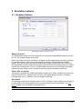
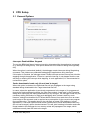
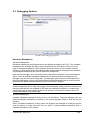
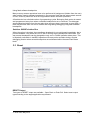
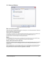
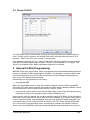
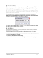
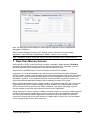
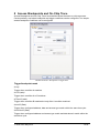
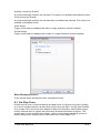
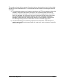
_ V9.12. 225 Technical Notes Freescale 68HCS08 Family On-Chip Emulation This document is intended to be used together with the CPU reference manual provided by the silicon vendor. This document assumes knowledge of the CPU functionality and the terminology and concepts defined and explained in the CPU reference manual. Basic knowledge of winIDEA is also necessary. This document deals with specifics and advanced details and it is not meant as a basic or introductory text. Contents Contents 1 1 Introduction 2 2 Emulation options 2.1 Hardware Options 2.2 Initialization Sequence 3 3 4 3 CPU Setup 3.1 General Options 3.2 Debugging Options 3.3 Reset 3.4 Advanced Options 3.5 Retain FLASH 5 5 6 7 8 9 4 Internal FLASH Programming 9 5 Trim Oscillator 10 6 Hot Attach 10 7 Real-Time Memory Access 11 8 Access Breakpoints and On-Chip Trace 8.1 On-Chip Trace 12 13 9 Getting Started 15 10 Troubleshooting 15 iSYSTEM, May 2015 1/15 1 Introduction The term BDM stands for Background Debug Mode. It is used for the system development and FLASH programming. A BDM firmware is implemented on the CPU silicon providing a comprehensive set of debug functionalities. Since BDM control logic does not reside in the CPU core, BDM hardware commands can be executed while the CPU is operating normally. The control logic generally uses CPU dead cycles to execute these commands, but can steal cycles from the CPU when necessary. Other BDM commands are firmware based, and require the CPU to be in active background mode for execution. While BDM is active, the CPU executes a firmware program located in a small on-chip ROM that is available in the standard 64-Kbyte memory map only while BDM is active. Debug Features The HCS08 BDM emulation system features: Up to three hardware breakpoints Unlimited software breakpoints, including in the internal FLASH Access breakpoints Real-time access Hot Attach Internal FLASH programming On-Chip Trace iSYSTEM, May 2015 2/15 2 Emulation options 2.1 Hardware Options Emulation options, Hardware pane Debug I/O levels The development system can be configured in a way that the debug BDM signals are driven at 3.3V, 5V or target voltage level (Vref). When 'Vref' Debug I/O level is selected, a voltage from the target debug connector connects to a voltage follower, which then powers debug tool buffers physically driving the BDM signals. The user must ensure that the target power supply is connected to the Vref pin on the target BDM connector and that the target is powered before the debug session is started. If these two conditions are not meet, the initial debug connection will most likely fail already. However in some cases it may succeed but then the system will behave abnormal. Check Vref on startup This option is available for iC5000 development system only. When checked, the system will check the presence of voltage on the Vref pin on the target debug connector. A warning message pops up if no voltage or too low voltage is detected, Hot Attach The debugger supports Hot Attach function. This is a function, which enables the emulator to be connected to a working target device and have all debug functions available. See Hot Attach chapter for more details on Hot Attach use. Note: Hot Attach function cannot be used for any flash programming or code download! iSYSTEM, May 2015 3/15 2.2 Initialization Sequence Before the flash programming or download can take place, the user must ensure that the memory is accessible. This is very important since there are many applications using memory resources (e.g. external RAM, external flash), which are not accessible after the CPU reset. In that case, the debugger must execute after the CPU reset a so called initialization sequence, which configures necessary CPU chip selects and then the download or flash programming can actually take place. The user must set up the initialization sequence based on his application. Detailed information may be found in the Initialization Sequence help topic. Note: Normally, there is no need to use the initialization sequence with HCS08 microcontrollers. iSYSTEM, May 2015 4/15 3 CPU Setup 3.1 General Options HCS08 Family Advanced CPU Options Interrupts Enabled When Stopped The on-chip BDM itself doesn’t support servicing interrupts while the application is stopped (e.g. interrupts in background). This option affects the CPU behavior during the single step only. When the option is unchecked (default), the debugger masks interrupts during Step debug command. This yields more predictable debugging of applications using interrupts. If this option is checked, the debugger doesn’t mask interrupts and an interrupt can hit while stepping through the application. If there is a periodic interrupt, it may happen that the user will keep re-entering the interrupt while stepping. In such applications, it’s recommended to uncheck this option. Cache downloaded code only (do not load to target) When this option is checked, the download files will not propagate to the target using standard debug download but the Target download files will. In cases, where the application is previously programmed in the target or it's programmed through the flash programming dialog, the user may uncheck 'Load code' in the 'Properties' dialog when specifying the debug download file(s). By doing so, the debugger loads only the necessary debug information for high level debugging while it doesn't load any code. However, debug functionalities like ETM and Nexus trace will not work then since an exact code image of the executed code is required as a prerequisite for the correct trace program flow reconstruction. This applies also for the call stack on some CPU platforms. In such applications, 'Load code' option should remain checked and 'Cache downloaded code only (do not load to target)' option checked instead. This will yield in debug information and code image loaded to the debugger but no memory writes will propagate to the target, which otherwise normally load the code to the target. iSYSTEM, May 2015 5/15 3.2 Debugging Options HCS08 Family Debugging Options Execution Breakpoints Hardware Breakpoints Hardware breakpoints are breakpoints that are already provided by the CPU. Four hardware breakpoints are available and they function anywhere in the CPU space, which is not the case for software breakpoints, which typically cannot be used in a non-writeable memory (ROM) or in applications with self-modifying code. When hardware breakpoints are selected, only hardware breakpoints are used for execution breakpoints. Note that the debugger, when executing source step debug command, uses one breakpoint. Hence, when all available hardware breakpoints are used as execution breakpoints, the debugger may fail to execute debug step. The debugger offers 'Reserve one breakpoint for high-level debugging' option in the Debug/Debug Options/Debugging' tab to circumvent this. By default this option is checked and the user can uncheck it anytime. The same on-chip debug resources are shared among hardware execution breakpoints, access breakpoints and on-chip trace trigger. Consequentially, debug resources used by one debug functionality are not available for the other two debug functionalities. In practice this would mean that no trace trigger can be set for instance on instruction address, when four execution breakpoints are set already. Software Breakpoints Available hardware breakpoints often prove to be insufficient. Then the debugger can use unlimited software breakpoints (including in the internal program flash) to work around this limitation. When a software breakpoint is being used, the program first attempts to modify the source code by placing a break instruction into the code. If setting software breakpoint fails, a hardware breakpoint is set instead. iSYSTEM, May 2015 6/15 Using flash software breakpoints Many memory access operations have to be performed in background (hidden from the user) when setting clearing software breakpoint in the program flash. As this takes certain amount of time, user may notice this as a time lag between certain winIDEA operations. A flash device has a limited number of programming cycles. Belonging flash sector is erased and programmed every time when a software breakpoint is set or removed. The debugger sets breakpoints hidden from the user also when a source step is executed. In worst case, a flash may become worn out due to intense and long lasting debugging using flash software breakpoints. Set/clear SW BPs before Run When the option is checked, then a software breakpoint is not set/cleared immediately, but is just remembered. Only when the CPU is set to running are the breakpoints committed. This way several breakpoints can be changed but only one re-FLASH operation takes place. This is especially noticeable in testIDEA operation with many stubs and also during a regular debugging session when several breakpoints are set/cleared within the same flash erase block. 3.3 Reset RESET Output Two types of RESET output are available – Open Drain or Push-Pull. Select reset output type according to the target application requirement. iSYSTEM, May 2015 7/15 3.4 Advanced Options HCS08 Family Advanced CPU Options Mass erase before download Check the option if complete flash should be erased prior to the debug download. Otherwise, only the necessary sectors are erased. Use monitor for programming If this option is checked, the FLASH is programmed through a special monitor loaded in the internal RAM; otherwise programming will be performed via BDM interface. It is recommended to check the option for better performance. Banks Some MC9S08 CPUs feature banks extending the internal flash beyond the 64 KB. Check the ‘Banked Application’ when the application is linked for bank operation. Resync SDI communication after Run Debug SDI interface must be synchronized with the microcontroller system clock. Per default only after every CPU reset the debugger synchronizes the debug SDI interface with the system clock. When the application run-time changes system clock, the debugger must resynchronized to the new system clock. When this option is checked, the debugger will resynchronize the debug SDI interface every time when the application is resumed. iSYSTEM, May 2015 8/15 3.5 Retain FLASH The CPU has a function which allows trimming the internal period of the internal reference clock. The trim value is stored in the internal flash and is internally read when the CPU is powered.. Refer to the CPU user manual for more details. If the address is checked, the Trim value is read before the flash programming and restored back after the flash programming completes. The size of trim registers is 1 or 2 bytes. This option is not available when ‘Mass erase before download’ is checked. 4 Internal FLASH Programming MC9S08 CPUs have internal flash, which is programmed through standard debug download; thereby no standard FLASH setup dialog is available. The debugger recognizes which code from the download file fits in the FLASH. All necessary FLASH programming settings are done in the ‘CPU Setup/Advanced’ dialog. Internal flash can be programmed in two ways: using regular BDM When the regular BDM mode is used, the emulator programs internal FLASH using BDM with writes to FLASH control registers and reads the status register. Because BDM is a serial communication this mode is much slower than the “monitor” mode. using a small monitor loaded in the internal RAM, which yields in fast flash programming comparing to the previous programming through the BDM port only When monitor mode is selected, the emulator requires internal CPU RAM. During the debug download, only the code which fits into internal FLASH is loaded. If you want to load a part of code to the internal RAM, ‘target download’ must be used. During the target download, only code which doesn’t fit into internal FLASH is loaded to the CPU. When regular BDM mode (the ‘Use monitor for programming’ option unchecked) is selected, the emulator loads the code to the internal RAM also during the download and the target download is not required. iSYSTEM, May 2015 9/15 5 Trim Oscillator This feature has been implemented on a customer request. The user may get a CPU without the trim value programmed in the dedicated flash location. Typically, this value is written in the flash by Freescale before the devices are shipped to the end customer. Currently, this feature is implemented for MC9S08SH devices only. Per default, the CPU has internal clock source with accuracy in range of 25%. To increase the clock source accuracy, the CPU provides the Trim register, which allows fine tuning the frequency of the internal clock source. The debugger performs the necessary measurements, calculates the trim value and programs it in the dedicated flash location when OK is pressed in the ‘HC08 Trim Oscillator’ dialog invoked via the ‘Hardware/Trim Oscillator’ menu. Keep default ‘Alternate BDC Clock Frequency’ in the dialog unless you have reasons to change it. Per default, when MC9S08SH device is selected, 32 MHz frequency appears in the dialog and 16MHz when MC9S08LG device is selected. 6 Hot Attach HCS08 BDM allows attachment to a running target system without affecting its operation. Such operation is called Hot Attach. It’s assumed that there is a running target with no debugger connected. To hot attach: Check the ‘Hot attach to target’ option in the ‘Hardware/Emulation Options/Hardware’ tab. Execute Download debug command. Connect the BDM cable to the target system Select the 'Attach' debug command in the ‘Debug’ menu to attach to the target system. iSYSTEM, May 2015 10/15 Now, the debugger should display run status and the application can be stopped and debugged if necessary. Select 'Detach' debug command in the ‘Debug’ menu to disconnect from the target application. If the CPU was stopped before detach, it will be set to running. Note: Hot Attach function cannot be used for any flash programming or code download! 7 Real-Time Memory Access With this type of CPUs, real-time memory access is available. Watch window’s Rt.Watch panes can be configured to inspect memory without stalling the CPU. Optionally, memory and SFR windows can be configured to use real-time access as well. Please refer to winIDEA Help for more information on Real-Time watches. In general it is not recommended to use real-time access for Special Function Registers (SFRs) window. In reality, real-time access still means stealing some CPU cycles. As long as the number of real-time access requests stays low, this is negligible and doesn't affect the application. However, if you update all SFRs or memory window via real-time access, you may notice different application behavior due to stealing too many CPU cycles. When a particular special function register needs to be updated in real-time, put it in the realtime watch window (don't forget to enable real-time access in the SFRs window but keep SFRs window closed or open but with SFRs collapsed). This allows observing a special function register in real-time with minimum intrusion on the application. Using “alternative” monitor access to update a memory location or a memory mapped special function register while the application is running works like this: the application is stopped, the memory is read and then the application is resumed. Hence the impact on real time execution is severe and use monitor access for 'update while running' only if you are aware of the consequences and can work with them. iSYSTEM, May 2015 11/15 8 Access Breakpoints and On-Chip Trace Access Breakpoints and On-Chip Trace functionalities share the same on-chip resources. Consequentially, equivalent breakpoint and trigger conditions can be configured. Two simple access breakpoint conditions can be configured. HCS08 Hardware Breakpoint Configuration Trigger/breakpoint mode A only Trigger when condition A matches. A or B (addr) Trigger when condition A or B matches A Then B (addr) Trigger when condition B matches but only after A condition matched. A and B (Data) Trigger when configured address, data and access type match within the same bus cycle. A and Not B (Data) Trigger when configured address and access type match and data doesn’t match within the same bus cycle. iSYSTEM, May 2015 12/15 Anything, record only B (data) All cycles matching B condition are recorded. This mode is not available as breakpoint mode. A then record only B (data) All cycles matching B condition are recorded after A condition has matched. This mode is not available as breakpoint mode. Inside Range Trigger occurs when the address falls within a range defined by A and B condition. Outside Range Trigger occurs when the address falls outside of a range defined by A and B condition. When Breakpoints Occur These options define the behavior when a breakpoint occurs. 8.1 On-Chip Trace HCS08 devices have no external address and data buses. A limited on-chip trace, typically an in-circuit emulator feature, has been built onto the chip with MCU. On-chip trace consists of an 8-stage FIFO, which can store address or data bus information, and a flexible trigger system to decide when to capture bus information and what information to capture. The system does not use any MCU pins. Rather, it relies on the background debug system to access debug control registers and to read results out of the 8-stage FIFO. iSYSTEM, May 2015 13/15 The number of words of bus capture information that can be stored at a time is limited (eight words in the first HCS08 devices). To compensate for this limitation, the debugger uses two strategies: 1) For tracking the sequence of program instructions, the FIFO only captures information related to instructions that cause a change to the normal sequential execution of instructions. With knowledge of the source code, which is programmed in the CPU flash, the debugger can reconstruct the path of execution through many instructions from the change-of-flow information stored in the FIFO. This allows an external debugger to reconstruct the flow through dozens or even hundreds of instructions from the eight change-of-flow events before or after a selected trigger point. 2) The second strategy is to selectively capture event information. This technique is used to capture only the data associated with read and/or write accesses to a specific address or register. iSYSTEM, May 2015 14/15 9 Getting Started 1) Connect the system 2) Make sure that the target debug connector pinout matches with the one requested by a debug tool. If it doesn't, make some adaptation to comply with the standard connector otherwise the target or the debug tool may be damaged. 3) Power up the emulator and then power up the target. 4) Execute debug reset 5) The CPU should stop on location to which the reset vector points 6) Open memory window at internal CPU RAM location and check whether you are able to modify its content. 7) If you passed all 6 steps successfully, the debugger is operational and you may proceed to download the code in the internal CPU flash. 8) Check ‘Erase before download' and 'Use monitor for programming' options in the 'CPU Setup/Advanced' tab. 9) Specify the download in the 'Debug/Files for download/Download files' tab. 10) Execute Debug download, which should download the code in the internal CPU flash. 10 Troubleshooting If BDM does start (system is initialized), but system cannot perform run or single step, check the BDM DSI line - there shouldn't be any strong pull-up - remove it and try again. Make sure that the power supply is applied to the target BDM connector when ‘Vref’ is selected for Debug I/O levels in the Hardware/Emulator Options/Hardware tab, otherwise emulation fails or may behave unpredictably. When performing any kind of checksum, remove all software breakpoints since they may impact the checksum result. Disclaimer: iSYSTEM assumes no responsibility for any errors which may appear in this document, reserves the right to change devices or specifications detailed herein at any time without notice, and does not make any commitment to update the information herein. iSYSTEM. All rights reserved. iSYSTEM, May 2015 15/15