1
PN532/C1
NXP Semiconductors
Near Field Communication (NFC) controller
CONFIDENTIAL
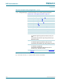
8.1.6 Timer0/1 description
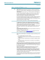
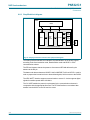
Timer0/1 are general purpose timer/counters. Timer0/1 has the following functionality:
•
•
•
•
Configurable edge or level detection interrupts
Timer or counter operation
4 timer/counter modes
Baud rate generation for Debug UART
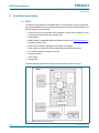
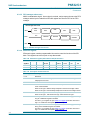
Timer0/1 comprises two 16-bit timer/counters: Timer0 and Timer1. Both can be
configured as either a timer or an event counter.
Each of the timers can operate in one of four modes:
•
•
•
•
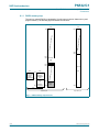
Mode 0: 13-bit timer/counter
Mode 1: 16-bit timer/counter
Mode 2: 8-bit timer/counter with programmable preload value
Mode 3: two individual 8-bit timer/counters (Timer0 only)
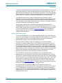
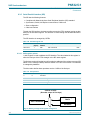
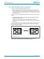
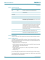
In the ‘timer’ function, the timer/counter is incremented every machine cycle. The count
rate is 1/6 of the CPU clock frequency (CPU_CLK).
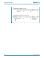
In the ‘counter’ function, the timer/counter is incremented in response to a 1-to-0 transition
on the input pins P34 / SIC_CLK (Timer0) or P35 (Timer1). In this mode, the external input
is sampled during state S5 of every machine cycle. If the associated pin is at logic 1 for a
machine cycle, followed by logic 0 on the next machine cycle, the count is incremented.
The new count value appears in the timer/counter in state S3 of the machine cycle
following the one in which the transition was detected. The maximum count rate is 1/12 of
the CPU_CLK frequency. There are no restrictions on the duty cycle of the external input
signal but to ensure that a given level is sampled at least once before it changes, it should
be held for at least one full machine cycle.
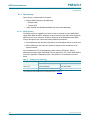
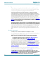
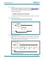
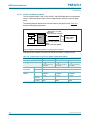
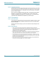
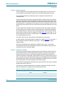
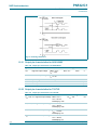
The overflow output ‘t1_ovf’ of Timer1 can be used as a baud rate generator for the Debug
UART. The Timer1 interrupt should be disabled in this case. For most applications which
drive the Debug UART, Timer1 is configured for ‘timer’ operation and in auto-reload mode.
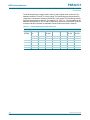
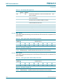
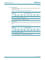
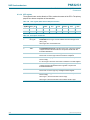
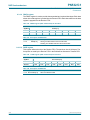
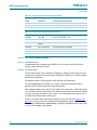
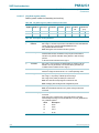
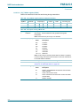
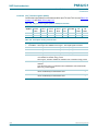
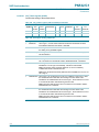
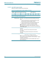
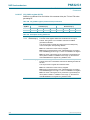
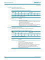
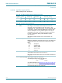
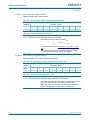
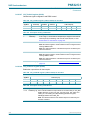
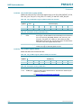
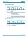
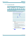
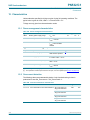
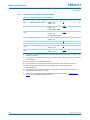
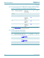
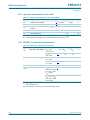
8.1.6.1 Timer0/1 registers
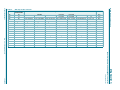
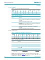
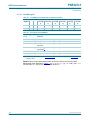
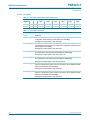
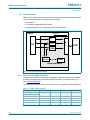
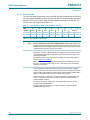
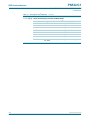
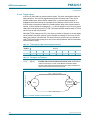
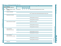
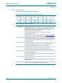
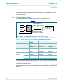
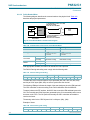
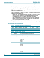
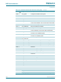
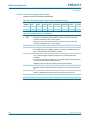
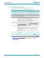
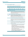
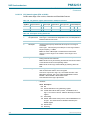
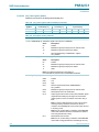
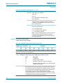
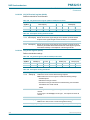
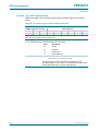
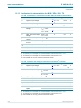
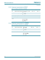
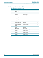
The Timer0/1 module contains six Special Function Registers (SFRs) which can be
accessed by the CPU.
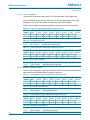
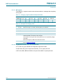
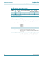
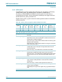
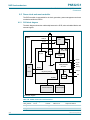
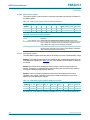
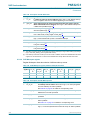
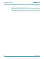
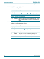
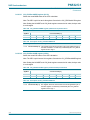
Table 20.
Timer0/1 Special Function registers list
Name
Size
[bytes]
Address
Offset
Description
Access
T01CON
1
88h
Timer0/1 control register
R/W
T01MOD
1
89h
Timer0/1 mode register
R/W
T0L
1
8Ah
Timer0 timer/counter lower byte
R/W
T1L
1
8Bh
Timer1 timer/counter lower byte
R/W
T0H
1
8Ch
Timer0 timer/counter upper byte
R/W
T1H
1
8Dh
Timer1 timer/counter upper byte
R/W
115432
Product data sheet
© NXP B.V. 2007. All rights reserved.
Rev. 3.2 — 3 December 2007
21 of 224