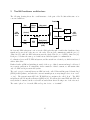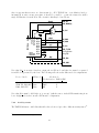
1
Neo900 NFC Subsystem Draft Werner Almesberger September 9, 2015 This document specifies the Near Field Communication (NFC) and Radio-Frequency IDentification (RFID) functionality of Neo900. TO DO: The focus is currently more on the evaluation and selection of suitable technology. We should change this later, when we’ve decided on a specific design. Please note that all this is based on reading the relevant standards (or drafts of them), data sheets, etc. None of the things described here have actually been tested by the author in an implementation. The document contains a large number of footnotes, acronyms, and citations. All these references have hyperlinks in the PDF version, which should make it easier to follow them when using the document for reference purposes. It is recommended to first read this document in its entirety in order to obtain an overview of the various topics discussed and how they are related. 1 1 High-level objectives We have the following expectations on the NFC solution for Neo900: Standards Although we currently have no specific “must have” use cases, we aim to be able to interoperate with equipment users will encounter labeled as “NFC”. In practical terms, this will most likely include NFC Type 2 tags [1] (using ISO 14443 Type A [2]), peer-to-peer communication according to NFC IP-1 [3] (using FeliCaTM [4] at “high-speed”), and ISO 14443 card emulation. Flexibility There are many protocol in the world of NFC and RFID, and any given solution is likely to miss some that may be relevant in certain use cases. We therefore aim to be flexible and give advanced users the option of adapting the NFC functionality of Neo900 to their needs. System environment The NFC solution must be suitable for the constrained environment found on a mobile phone. This includes the use of system-internal communication interfaces such as I2 C operating at 1.8 V, low-power standby, and also low power consumption when waiting for the device to enter the field of an NFC or RFID reader. Linux driver The hardware must have good driver and protocol stack support in Linux, without adding a major development burden to the Neo900 project. Hardware documentation Hardware documentation sufficiently in-depth to enable the Neo900 project to correctly implement the NFC circuit must be available – preferably without NDAs or similar obstacles. Privacy In line with our general emphasis on privacy and user empowerment, we aim to ensure that the NFC subsystem will not communicate without the user’s express consent. In particular, it must either lack the ability of field-powered operation or there must be a mechanism that allows users to suppress this mode of operation. Tweakable Wherever practical, advanced users should be given access to low protocol layers not only in order to allow the addition of support for new protocols, as mentioned above, but also for experiments with the design and implementations of the protocols themselves. 2 2 Communication modes This section gives a very brief introduction to the communication modes used in the context of NFC/RFID with the following drawings illustrating the various scenarios. The “reader” is also called “reader/writer”, and in the various ISO standards Proximity Coupling Device (PCD), Vicinity Coupling Device (VCD), or “interrogator”. The “card” is often called a “tag”, and ISO also uses Proximity Integrated Circuit Card (PICC) and Vicinity Integrated Circuit Card (VICC). We will use mainly the terms “reader” and “card” or “tag”. 2.1 Reader and card The basic model is to have a reader and a card or tag. The reader is connected to a power source, is often part of a fixed installation, and generates a strong electromagnetic field whenever it is looking for cards (which it may be expected to do most of the time). The card is mobile and has no power source of its own. Instead, it is powered by the field the reader generates. A the card that is not near a reader receives no power and is therefore not operational. Power Power, data Reader Reader Card(s) Card(s) Data Amplitude modulation Load modulation The reader sends data to the card (drawing on the left) by modulating the field it emits. It typically uses some form of Amplitude Modulation (AM), though other modulation schemes are possible. The card sends data to the reader (drawing on the right) by changing the characteristics of its receiver and thus modulating the field created by the reader. This is called load modulation. If there are multiple cards in the vicinity of a reader, their transmissions may overlap (“collide”) and the reader therefore has to select a single one for communication. This process is called “anticollision” and is described in more detail in section 3.4. 2.2 Card structure In addition to the radio interface and associated protocol processing, an NFC/RFID card contains also additional elements, as shows in the following drawing: 3 NFC/RFID card Reader RF UID Memory SE In a very simple application, a card will just have a unique ID (UID) and a reader merely queries this ID. A more sophisticated application would use a challenge-response scheme to prevent others from impersonating the card. A card can have additional memory that can be read and possibly also written by the reader (or reader/writer). Such memory can for instance contain publicly accessible information such as a product code, a URL, an image, etc. Last but not least, a card may contain a Secure Element (SE). This is provides an isolated execution environment for security-sensitive applications, such as authentication protocols for electronic payment. 2.3 Card emulation Card emulation is similar to the previous scenario, except that we have a smartphone in the role of a card. The smartphone may use its own power source but its NFC/RFID subsystem may also be capable of operating with power from the field alone. Power, data Reader Secure element Amplitude modulation Communication is exactly the same as with a card: the reader modulates the field to send data to the phone, and the phone modulates the field by changing its load characteristics to respond. Power Reader Secure element Data Load modulation 4 If the application requires a SE, then this may be provided either as part of the smartphone’s hardware, by software, or through a Subscriber Identity Module (SIM) card. In the latter case, the NFC/RFID subsystem acts merely as a relay between the radio interface and the SIM card, with the SE controlling most of the protocol processing. We discuss the mechanism used for communication between the secure element in the SIM card and the smartphone in section 6. Note that a smartphone can also act as reader, communicating with a card or with another smartphone using card emulation. 2.4 NFC peer-to-peer When both parties are smartphones or similar devices, they can also use NFC peer-to-peer communication. Unlike a card reader that will typically continuously scan for cards, an NFC device only activates its field when requested to do so. A device can act as “initiator” (activates field and then searches for peer) or as “target” (wait for an initiator to begin communicating). Field, data Target Initiator Amplitude modulation Communication between initiator and target can be as if they were reader and card, respectively, with the initiator providing the field and the target modulating it. The main difference is that the target has its own power supply and thus does not depend on the presence of an initiator to operate. Field Target Initiator Data Load modulation The above is called “passive” mode. Since both devices are capable of producing an electromagnetic field, there is also an “active” mode, depicted below. 5 Amplitude modulation Initiator Target Field, data In this mode, the initiator deactivates its field when it is done sending and the target generates its own field to send a response. I.e., this is how radio communication normally works, with each party providing the electromagnetic field needed for its transmissions. 6 3 Protocol architecture There are four major protocol families in NFC: RFID for “dumb” tags, defined in ISO 18000 [5]. Proximity cards with a range of up to about 10 cm, defined in ISO 14443 [6, 7, 8]. Vicinity cards with a range of up to about 1 m, defined in ISO 15693 [9, 10]. NFC for tags [11] but also for devices that can act as equals, defined in [3]. NFC also covers interoperation with the above standards, in [12]. All four stacks are based on the 13.56 MHz ISM band. Each then defines a modulation and encoding scheme. We briefly discuss these in section 3.3. At the next layer are framing and anti-collision, which we cover extensively in section 3.4. On top of everything is the actual user of the stack, which may in turn be another stack of more protocols. The following diagram shows the overall structure of the NFC protocol stack, with protocol variants within the same family and relations between families: Proximity ISO14443 Vicinity ISO15693 RFID ISO18000 Framing fc/64, ... Band Modulation User NFC Device NFC IP−1 fc/64, ... FeliCa FeliCa fc/128 Type A fc/128 Annex C Type B ISO14443−2 Type A ISO18000−3 Mode 1 Extensions non−slot slotted ISO15693−3 ISO14443−3 ISO15693−2 Type B 256/fc 4/fc Subcarrier single dual Mode 2 ISO18000−3 Mode 2 13.56 MHz (HF) Where protocols are shared across families, the origin of the protocol is shown with a grey background. For example, ISO 18000-3 Mode 1 without extensions uses the anti-collision protocol defined in ISO 15693-3. Proprietary protocol variants like MIFARETM or FeliCaTM are not shown. 3.1 Names and aliases of standards The ISO standards often have names of the form standard family–part. In the case of ISO 14443, the numbering of the parts (–2 to –4) could be misunderstood as representing OSI layering. This is not the case, and as the example of ISO 18000 shows, the same standard document may cover layers that are split into multiple parts in a different family. 7 Furthermore, protocol variants described in the same standards document can be radically different from each other and do not have to be interoperable. For example, it is perfectly acceptable for a standards-compliant ISO 18000-3 Mode 1 device to be unable to communicate with a standardscompliant ISO 18000-3 Mode 2 device.1 According to [13], the division of ISO 14443 into an A and a B type mirrors the two competing advocates, NXP (type A) and Texas Instruments (type B). Sony unsuccessfully tried to establish an ISO 14443 Type C and then created FeliCaTM (similar to ISO 14443-2 Type B with ISO 14443-3 Type A annex C on top). Some standards go by many names. For instance, NCF IP-1 [3] is known as ISO/IEC 18092 and ECMA-340, and one of the protocol variants it specifies (fC /128) just reuses ISO/IEC 14443 Type A for its lower layers. Also note that ISO 18092 (NFC) is very different from ISO 18000 (RFID tags). Among other protocols, [14] specifies the following underlying standards for protocols of the various tag types defined by NFC Forum: Type 1 2 3 4A 4B 3.2 [15] [1] [16] [17] [17] Basis NFC-A NFC-A NFC-F NFC-A NFC-B Standard NFC IP-1 [3], meaning NFC IP-1 [3], meaning NFC IP-1 [3], meaning NFC IP-1 [3], meaning ISO 14443 Type B ISO 14443 Type A ISO 14443 Type A FeliCaTM ISO 14443 Type A Bit rates Timings in NFC are usually expressed in terms of the carrier frequency fC = 13.56 MHz, with subcarrier frequencies and data rates using the notation fC ⁄n and bit durations n⁄fC . The following table shows the most commonly used rates, the corresponding bit durations, and also mentions the most relevant standard(s) using that rate: 1 Emphatically stated several times in sections 1.3, 6.0.1 to 6.0.4, 6.1, and 6.2 of [5]. 8 Divider n 2048 2032 512 508 128 64 32 16 Bit rate fC ⁄ n kbps 6.62 6.67 26.48 26.69 106 212 424 848 Bit duration n⁄f C µs 151 150 38 37 9.44 4.72 2.36 1.18 Used by . . . ISO 15693, low rate, single subcarrier dual subcarrier high rate, single subcarrier dual subcarrier ISO 14443 ISO 14443 (after anti-collision), FeliCaTM ISO 14443 (after anti-collision) ISO 14443 (after anti-collision) NCF IP-1 stretches the rules of FeliCaTM2 a little and allows rates up to 3.3 fC ⁄32.3 Modulation and coding In this section we briefly summarize the lower layers of NFC radio protocols. This overview is intended to provide context for the following sections and also to better understand the capabilities and limitations of the chips we examine later on. All RFID/NFC devices in the HF band operate with a carrier frequency of 13.56 MHz ± 7 kHz. Since the RF field of the reader also provides power to cards, the communication protocols used in the reader to card direction try to keep the field reasonably constant: Protocol ISO 14443-2 ISO 15693-2 ISO 18000-3 FeliCaTM NFC IP-1 Variant Type A Type B 256⁄fC 4⁄fC Mode 1 Mode 2 fC ⁄128 other Modulation Coding ASK 100% modified Miller ASK 10% NRZ ASK 10 or 100% PPM 1⁄256 ditto PPM 1⁄4 see ISO 15693-2 PJM MFM ASK 10% Manchester see ISO 14443-2 Type A see FeliCaTM In the opposite direction, the card uses load modulation and the protocols typically aim to produce a stable regular pattern throughout each bit duration: 2 3 Sections 5.2.1 and 5.3.1 of [4]. Section 9.2.2.1 of [3]. 9 Protocol ISO 14443-2 ISO 15693-2 ISO 18000-3 FeliCaTM NFC IP-1 Variant Type A, fC ⁄128 other single subcarrier dual subcarrier Mode 1 extensions Mode 2 fC ⁄128 other 3.4 Modulation Coding OOK Manchester BPSK NRZ OOK — FSK — see ISO 15693-3 BPSK/OOK — BPSK MFM OOK Manchester see ISO 14443-2 Type A see FeliCaTM Anti-collision Anti-collision is the process of identifying individual cards or tags (PICC or VICC) in a set of cards or tags that have been brought into the RF field of a reader (PCD or VCD), and then activating one or more specific cards for further communication. This section summarizes the anti-collision mechanisms used by the protocols specified for RFID and NFC. The main objectives are to provide a rough overview of the variety of protocols and to determine – at a qualitative level – what kind of timing requirements would exist for software implementations of the respective protocols. We pay special attention to anti-collision since this is the part of the various NFC and RFID protocols that is most likely to involve delicate timing (e.g., precise detection of collisions at the bit level, see section 3.4.1) and complex modulation schemes (e.g., On-Off Keying (OOK) and Phase-Shift Keying (PSK) in the same message, see section 3.4.6). This in turn determines what hardware capabilities we require from NFC chips in order to handle a given protocol, and what software-based solutions have to do if trying to support a protocol that is not fully supported by hardware. 3.4.1 ISO 14443-3 type A ISO 14443-3 type A uses an anti-collision algorithm where cards whose addresses match a prefix provided by the reader respond by sending their (unique) addresses bit-synchronously. The reader detects collisions at the bit level, grows the prefix accordingly, and repeats this process until one card has been fully identified. For example, a reader would first initiate the anti-collision sequence by sending an REQA or WUPA command, to which all suitable type A cards respond with an ATAQ message. The reader would then send an ANTICOLLISION (AC) command with a prefix of length zero. All cards simultaneously respond with their addresses, producing collisions on some bit positions. The reader adds the collision-free bits to the prefix, picks 0 or 1 for the next bit, and sends a new AC command 10 for the new prefix. This is illustrated in the following diagram where cards A and B match the prefix but then collide in the last two bits: AC(t) AC Prefix length 4 0 0 1 0 Match A 0 0 1 0 0 0 0 1 B 0 0 1 0 0 0 1 0 Card response Collision 0 0 1 0 0 0 Learn C AC(t+1) 0 0 1 1 0 1 0 1 AC Card addresses 7 0 0 1 0 0 0 0 Old prefix Pick 0 or 1 Received From a card’s point of view, the sequence ends when the prefix matches the entire address of the card (in which case the AC command is called SELECT) and the card then acknowledges this with a SAK (select acknowledge) response. The protocol is described in detail in sections 6.3 through 6.5 of [7]. 3.4.2 ISO 14443-3 type B ISO 14443-3 type B uses a slotted anti-collision mechanism where the effect of collisions can be observed at the frame level. The reader begins each anti-collision sequence by sending a WUPB(N) or REQB(N) command with parameter 1 ≤ N ≤ 16. Each card then picks an individual random number 1 ≤ R ≤ N . If R = 1, it immediately sends an ATRB response, possibly colliding with responses from other cards. The reader can then send slot markers SM(s) for 2 ≤ s ≤ N to which cards respond if R = s (using the random number generated upon reception of WUPB/REQB). The reader can suppress further anti-collision responses from a card by activating it with ATTRIB or by silencing further responses to REQB with the command HLTB. The reader performs the anti-collision sequence whenever it is looking for new cards or when trying to enumerate a set of cards that has entered its RF field. The protocol is described in detail in sections 7.3 through 7.10 of [7] and more accessibly in Atmel’s excellent summary [18]. Atmel also expands that this mechanism exists in two flavours, probabilistic4 and slotted, which differ in whether the reader sends slot markers to probe cards with R > 1 or whether it just uses successive random number draws until every card has chosen R = 1 and thus responded in the first slot. 4 As shown in the example in annex D of [7]. 11 3.4.3 ISO 14443-3 type A annex C Not to be outdone by type B, type A also has an optional slotted anti-collision protocol, described in annex C of [7]. Like in type B, cards respond in randomly selected time slots, but with the difference that time slots are not explicitly signaled by the reader but instead determined by the time that has passed since the REQ-ID command that starts the whole time slot sequence. While there is no direct command to silence a card, a card that has been identified and activated will remain silent after concluding operation according to ISO 14443-4.5 3.4.4 FeliCa FeliCaTM [4] has basically the same anti-collision protocol as ISO 14443-3 type A annex C (section 3.4.3), but with a different message structure and a reduced set of message types. 3.4.5 ISO 15693-3 The anti-collision mechanism defined in section 8 of ISO 15693-3 [10] combines a prefix mechanism with slots. Like in ISO 14443-3 type A (section 3.4.1), the reader sends an inventory request containing a prefix for the card ID. The cards with matching addresses then respond with their full ID in the respective slot corresponding to the four bits of their ID that follow the prefix. This is similar to ISO 14443-3 type A annex C (section 3.4.3), except that the slot number is not random. Collisions are detected at the frame level in each slot. Slot numbers are not explicitly signaled by the reader, but instead each card keeps a local slot counter and increments it when the end of a slot is indicated. If a card sees more slots being signaled than expected in a round, it simply ignores the extra slots.6 Besides the “Inventory” command, there are also the usual commands for resetting the anti-collision protocol state (“Reset to ready”), to silence a specific card (“Stay quiet”), and to select a card for further communication (“Select”).7 Card selection is not required for communication but allows to omit the card’s ID in further messages.8 3.4.6 ISO 18000-3 mode 1 ISO 18000-3 mode 1 uses ISO 15693-3 anti-collision9 but also features a protocol extension that comes in two major branches called “non-slotted non-terminating multiple tag reading” and “slotted terminating adaptive round multiple tag reading”.10 5 6 7 8 9 10 Section C.3 of [7], and also shown in figure C.1 in section C.5. Figure 9 in section 8.2 of [10]. Sections 9.2.1, 9.3..7, 9.2.2, and 9.3.6 of [10], respectively. Section 7.2.3 of [10]. Section 6.1.2 of [5]. ISO 15693 is included in ISO 18000-3 as annex G. Sections 6.1.10.2 and 6.1.10.4 of [5]. 12 Non-slotted extension The non-slotted extension is refreshingly simple and consists of a Wakeup11 command from the reader, which then causes tags to send their default replies12 randomly and repeatedly as long as they remain in the field. While timing is not specified, it is recommended that Time between replies Duration of reply ≈ 10. The reader simply listens for any responses and uses those that are not garbled. Slotted extension The slotted extension is somewhat similar to ISO 14443-3 type B (section 3.4.2) in that cards respond in randomly selected slots and that slots are explicitly announced by the reader. Like in ISO 15693-3, cards keep a local slot count that advances at the end of the slot. It differs in that slot counters of tags wrap around – with the drawing of a new random number – at the highest slot number. Different tags may use different highest slot numbers, but the reader can also command a common slot number range.13 A reader responding in a slot sends a two-part response consisting of a so-called precursor used for collision detection,14 followed by the actual response.15 If a collision is detected, the reader can either end the slot after the precursor (the cards have to turn around and listen between precursor and main reply) or by indicating an error at the end of the regular slot duration.16 While the timing of whole slots is provided by messages sent by the reader, the phases inside a slot (i.e., precursor, possible early termination, main reply) are determined by the time since the beginning of the slot.17 3.4.7 ISO 18000-3 mode 2 ISO 18000-3 mode 2 is designed to work with very large tag populations in the same field18 and differs substantially from all the above protocols. It uses a novel modulation scheme for a single communication channel from the reader to cards,19 and eight reply channels distinguished by their subcarrier frequencies for card responses.20 Readers may receive on all eight channels simultaneously but can also support only operation on a single channel.21 Last but not least, tags can be 11 12 13 14 15 16 17 18 19 20 21 Section 6.1.11.2.13 of [5]. Sections 6.1.10.16 and 6.1.10.17 of [5]. The general sequence is defined in sections 6.1.10.4 and 6.1.10.7 of [5]. The commands are defined in the following sections: Wake-up (begins a round), 6.1.11.2.12; Next-slot, 6.1.11.2.1 through 6.1.11.2.3; New-round-size (sets new highest slot number and resets the slot counters in tags), 6.1.11.2.16. Message sequence in section 6.1.10.10, precursor format in 6.1.10.12, PSK of sub-carrier for the leader in section 6.1.10.18.2, and OOK for the collision detection sequence in sections 6.1.10.18.3 and 6.1.10.18.4. Sections 6.1.10.10 and 6.1.10.11 for the message sequence, 6.1.10.16 and 6.1.10.17 for the main reply format, PSK in section 6.1.10.19. Explained in section 6.1.10.5, the “ultimate-error” command is described in section 6.1.11.2.7. Figure 4 and table 2 in section 6.1.10.5 of [5]. Table 26 in section 6.2.6 of [5] mentions a tag inventory of more than 32 000 tags. Phase Jitter Modulation (PJM), see annex A of [5]. Section 6.2.3.3.1 of [5]. Section 6.2.7.3.1, example in section 6.2.7.8. Single channel selection is described in table 20 in section 6.2.5.16.3.2. 13 randomly muted22 or they can be individually ordered to remain silent.23 There are only two command types: read and write. There is no slotting. 3.4.8 ISO 18000-3 mode 3 A third mode was added to ISO 18000-3, for which no freely available information could be found. 3.4.9 NFC IP-1 An NFC initiator performs CSMA/CA, i.e., it can activate its RF field only if it does not detect the presence of another field.24 This is called “RF collision avoidance.” In passive mode, this only affects access to the ether, but in active mode, RF collision avoidance is also used for selecting a target (i.e., the one with the shortest random delay).25 In passive mode at fC ⁄128, NFC uses ISO 14443-3 type A anti-collision (section 3.4.1) with a new codepoint indicating NFC in the SAK message sent by the NFC target.26 In passive mode at 3.4.10 fC ⁄64 and fC ⁄32, NFC uses FeliCaTM .27 Summary The following table summarizes the key characteristics of the various anti-collision mechanisms: Protocol ISO 14443-3 FeliCaTM ISO 15693-3 ISO 18000-3 NFC IP-1 22 23 24 25 26 27 Variant Type A Type B Annex C Mode 1 non-slot extension slot extension Mode 2 fC ⁄128 other Separation Prefix Random slot Random slot Random slot Prefix, deterministic slot see ISO 15693-3 Random delay Random slot Random channel, mute see ISO 14443-3 Type A see FeliCaTM Time-based Bit collision — Slot Slot — — Phase in slot — Section 6.2.7.3.2.2, example in section 6.2.7.9. “Fully muted” in section 6.2.7.3.2, “temporarily muted” in the example in section 6.2.7.8. The mechanism for putting a tag in fully muted state is described in section 6.2.5.16.7, the corresponding code point is in table 20 of 6.2.5.16.3.2. Section 11.1.1 of [3]. Section 11.3 of [3]. Section 11.2.1 of [3]. Section 11.2.2 of [3]. 14 “Separation” is what prevents multiple cards from always replying at the same time. “Time-based” describes the element of the anti-collision protocol that has the tightest timing requirements. 3.5 Framing Framing of messages in the various NFC protocols is not covered in this document. The chips we discuss later implement some types of framing in hardware and usually provide some form of “raw” access to the radio interface to allow external digital hardware to implement codings and framings the respective NFC chip does not support natively. 3.6 Higher layers There can be many additional protocol layers on top of anti-collision and framing, particularly in the case of NFC peer-to-peer operation. See for example figure 1 in section 1 of [19], with additional details in figure 14 in section 6.28 “Smart” NFC chips may implement some elements from these protocols while “dumb” chips will just pass frames to the host and let it take care of the rest. 28 The same document also serves as a warning against overly optimistic expectations regarding interoperability: the experimental results in section 9 show that the chances for successful peer-to-peer communication with contemporary smartphones were rather low when using anything other than NFC-F and the smartphone acting as initiator. 15 4 Available protocol stacks A surprisingly large number of NFC stacks is available for Linux. They can be characterized as follows: [20] libnfc-nxp NXP-centric vendor stack for Android. https://android.googlesource.com/platform/external/libnfc-nxp/ Open NFC Another vendor stack, this time from Inside Secure. http://open-nfc.org/ librfid The user-space stack of the OpenPCD project. Now defunct and replaced by libNFC. http://www.openpcd.org/Host_Software#librfid libNFC Community project developing a user-space stack centered on the NXP PN53x chip family.29 http://nfc-tools.org/ Linux NFC Kernel-based vendor-neutral (at the time of writing, the stack had drivers for devices from Inside Secure, Marvell, NXP, Sony, STM, and Texas Instruments) stack, following the regular development model for the Linux kernel. https://01.org/linux-nfc The kernel-based Linux NFC project clearly looks like the future and we can probably safely ignore the other projects. 29 http://nfc-tools.org/index.php?title=Devices_compatibility_matrix 16 5 Neo900 hardware architecture The following drawing shows the overall structure of the part of the Neo900 architecture we’re concerned with here: Terminal USB/UART CPU DM3730 Host Modem PHS8/... Data, power ETSI TS 102 211 (Control) (TBD) Data (TBD) (Control) NFC CLF Data, power Switch Data Data, power #1 SIM UICC Card #2 Data, (power) ETSI TS 102 613 (SWP) Modem and NFC subsystem both access the SIM cards through a switch that distributes data signals and power from both sources to the cards. The modem communicates with the protocol defined in [22], while the NFC subsystem uses the Single Wire Protocol (SWP) defined in [23]. Both protocols share the same power rails but use different signals for communication. Coordination between CPU, NFC subsystem, and the switch is not defined yet, which is indicated with a dashed line. Further details on SIM card switching is outside of the scope of this document and may be addressed in a separate publication. For simplicity, in the remainder of this document, we will assume that only one SIM card is present in the system. The card or tag is commonly known as SIM but is also called Universal Integrated Circuit Card (UICC) in ISO parlance, and when the context is unambiguous, we may simply refer to it as “card” or “tag”. The system’s main CPU, the TI DM3730, is sometimes also called “host”. The NFC subsystem is called ContactLess Frontend (CLF) in [23]. We will use the terms UICC and CLF only rarely in this document, but the reader will encounter them when following some of the references. The entire “phone” is – from the SIM card’s point of view – a “terminal”. 17 6 SWP As its name suggests, the Single Wire Protocol consists of a single wire (called SWIO) connecting the NFC subsystem and the SIM: VCC NFC SIM S1 (V) SWIO Secure Element S2 (I) The lower layers of SWP are defined in [23]. It is intended to convey configuration data and radio messages related to ISO 14443-3 type A [7] and NFC IP-1 [3] between NFC and the Secure Element in the SIM. Bidirectional communication is made possible over this single wire by using voltage signaling (signal S1) from NFC to SIM, and current signaling (signal S2) from SIM to NFC. Section 6.3 contains a detailed illustration of this process. 6.1 Voltages The supply voltage of the SIM card for SWP use has to be30 either class B or C, which are defined as 2.7–3.3 V and 1.62–1.98 V, respectively.31 The voltage on SWIO is confusingly defined as either absolute (class B and sometimes class C) or relative to VCC (class C).32 The following table summarizes the voltage levels at the card interface, for simplicity assuming VCC in class C to be exactly 1.8 V: Voltage Class VOH B C B C B C B C VOL VIH VIL 30 31 32 Absolute (V) Min Max 1.40 1.98 1.53 1.8 0 0.3 0 0.27 1.13 2.28 1.26 2.1 –0.3 0.48 –0.3 0.45 × 1.8 V Min Max 0.78 1.1 0.85 1 0 0.17 0 0.15 0.63 1.27 0.7 1.17 –0.17 0.27 –0.17 0.25 Section 7.1.1 of [23]. Sections 5.2.1 and 5.3.1 of [22]. Tables 7.3 and 7.4 in section 7.1.3 of [23]. 18 Values defined by the standard are shown in boldface, the other values are calculated. Note that VIH must be guaranteed for currents up to 1000 µA (into the card) and VIL for currents up to −20 µA.33 It is confusing that the standard would specify output and input voltages, given that SWIO is voltage-operated in one direction and current-operated in the other, and one would therefore expect input and output to be identical as far as voltages at this interface are concerned. 6.2 SWIO states We can combine the worst-case voltage requirements from above with the possible states of S1 and S2 and the corresponding currents that may flow: S1 L H H S2 — 0 1 Voltage (V) < 0.27 ≥ 1.53 ≥ 1.53 Current (µA) ≤ 20 ≤ 20 600–1000 For example, the interpretation of S1=H, S2=1 is that the host must be able to detect an S2=0 condition if the card draws at least 600 µA, and that the voltage at the card’s SWIO pin must be at least 1.53 V if the card draws up to 1 mA. Note that these worst-case requirements are probably too strict and lead to an operating point very close to the supply voltage . If we decide to use more relaxed bounds, the circuit will be able to have larger tolerances margins. 6.3 SWP bit encoding The default bit duration is 1–5 µs.34 Each bit period begins with a rising edge on SWIO and a high level of 1/4 (to send a “0” on S1) or 3/4 (to send a “1’), followed by the falling edge and a low level until the end of the bit period. The following diagram illustrates transmission on S1 and S2. For simplicity, we use a nominal bit time of 4 µs, a nominal voltage of 1.8 V, and a nominal high current of 800 µA (800 ± 200 µA). 33 34 Table 7.5 in section 7.1.4.1 of [23]. Table 8.1 in section 8.1 of [23]. 19 T T T 4 µs 1.8 V 0V 1/4 T 3/4 T 1 µs 3 µs 3/4 T 0 S1 1/4 T 3/4 T 1 1/4 T 1 800 µA 0 mA 0 S2 1 0 switch load The card switches its load characteristics while SWIO is low, and the state of S2 is only defined while SWIO is high. Further details can be found in section 8 of [23]. Depending on implementation constraints, one may prefer a faster or a slower bit rate than indicated in the example above. A low rate may be preferable if the CPU is unable to toggle IO pins quickly or if measuring the S2 signal is slow. A fast rate may be preferable for more rapid communication and if there are large positive delay variations on CPU operations, e.g., caused by background activity such as cache or DMA operations. 6.4 S2 current detection Devices what would allow direct detection of currents that result in only small voltage changes are not commonly available in SoCs or MCUs. A simple circuit to measure the S2 current would involve a series resistor on SWIO that acts as shunt, and an analog comparator or similar that compares the resulting voltage drop against a threshold voltage. The following diagram shows a common configuration of such a circuit: CPU (CLF) Vio Card (UICC) Iswp Ron SWP_OUT Rshunt Icard SWIO (C6) Vswp Vcard Icmp Vth SWP_IN 20 In this circuit, the comparator would output a “1” if VCARD < VTH − (VH + VOFF ) and “0” if VCARD > VTH + VH + VOFF with VCARD = VIO − (RON + RSHUNT ) · (ICARD + ICMP ) and the following parameters: Parameter VIO VH VOFF RON RSHUNT ICARD ICMP Description Supply voltage for SWP OUT driver Hysteresis (may be zero) Comparator offset voltage On-state resistance of SWP OUT driver Resistance of external shunt resistor Current drawn by the card’s SWIO pin Input leakage current of the comparator To permit reliable detection of S2 states, we therefore need (RON + RSHUNT ) · 580 µA ≥ 2 · (VH + VOFF ) where 580 µA is the difference between the minimum current at S2=1 and the maximum current at S2=0, or VH + VOFF RSHUNT ≥ − RON 290 µA Furthermore, to meet the voltage level requirements from section 6.2, we need: RSHUNT ≤ VIO − 1.53 V − RON 1000 µA + ICMP and RSHUNT ≤ 0.27 V − RON 20 µA + ICMP The DM3730 contains no analog elements and the ADC in the TPS65950 companion chip has conversion times of tens of microseconds, which would be far too slow for SWP.35 35 Table 5-77 in section 5.6.3.1 of [24]. 21 To implement a detection circuit similar to the above example, a comparator external to the CPU would be needed. This could be in the form of a dedicated chip or by using a comparator circuit in another system component. Section 8.5 discusses a possible configuration using the built-in comparator of a Kinetis KL16 or KL26 series MCU. 6.5 SIM card power and card activation This section discusses the card activation process, i.e., provisioning of power and the communication required before an SWP interface can be used. We also consider the role of the modem and the consequences of sharing a SIM card between modem and NFC. 6.5.1 Card activation The SWP standard defines36 card power-up (“activate the contact C1 (Vcc)”) such that communication over the SIM’s RST (C2), CLK (C3), and I/O (C7) pins is required. Furthermore, the availability of SWP functionality in the card is also signaled over the same interface.37 From this it would seem that any SWP user must either have the ability to communicate with the SIM over the regular data interface directly, or be able to coordinate SIM power-up and capabilities with the entity that controls this interface, i.e., the modem. However, SWP use by field-powered NFC chips, e.g., the PN54438 , suggests that the SWP part of a SIM is also expected to be operational without prior activation of the SIM. This is also consistent with what is shown in section 6.2.3 of [23]. 6.5.2 Role of modem Unfortunately, we found no indication in [27] that the modem would allow the host to control SIM activation, or that the modem would give access to the ATR information (including SWP support) obtained from the card during activation. There is also no separate hardware interface that would allow a 3rd party to request SIM activation.39 Also after activation, the fate of the SIM card is uncertain: while it seems unlikely that the modem would decide on its own to power down the card completely, it can enter clock stop mode with a reduced current consumption of 100 µA.40 36 37 38 39 40 Section 6.2.2 of [23], referring to section 4.5.2.1 [22], which in turn invokes the procedure defined in section 6.2 of [25]. According to section 5.3 of [23], UICC-side support is indicated in the “Global Interface” bytes in the ATR (Answer to reset) defined in section 7 of [25] using the encoding from table 6.7 in section 6.3.3 of [22]. Terminal-side SWP capability is communicated at a later point. Section 10.6.4 of [26]. Table 22 in section 6.5 of [28]. Clock stop is defined in section 6.3.2 of [25] and the corresponding power consumption is defined in sections 5.2.1 (class B) and 5.3.1 (class C) of [22]. 22 However, this reduced power consumption is only applicable if no other interfaces (such as SWP) are active. Since the modem has no way of knowing whether this is the case, we may have to assume that it expects the SIM card to adhere to the 100 µA limit when in clock stop mode. 6.5.3 Activation process The following drawing summarizes the activation process: Terminal (Modem, etc.) VCC RST, CLK, I/O SIM/UICC ATR ... SWIO ACT ... The terminal (modem, etc.) first applies the lowest available voltage to the SIM card. The card may then send an ATR message on the serial interface using CLK and I/O. If the terminal receives no message, it switches to the next higher voltage, waits again for an ATR message, and so on. Once ATR has been received, card and terminal can communicate some more over the same interface. Once this initial dialog has concluded, the SIM card is fully operational and the terminal can proceed with activating the SWP interface. To do this, it raises the SWIO pin and then waits for a response using ACT (ACTivation protocol). If no ACT response arrives, the terminal can try to raise the SIM card by sending an ACT frame on its own, but [23] has no provision for negotiating a voltage.41 We can conclude from this that the standard clearly expects that any user of SWP will be able to cooperate closely with the modem when it comes to card activation. 6.5.4 Avoiding deactivation Section 10.6.4 of [26] describes that the chip is able to supply the card with 1.8 V when the phone is deactivated. From the available description it is not clear whether this is expected to work also in cases where the card has not been previously activated through the modem. Since deactivation by the modem42 requires the removal of power, it should be possible to retain access to the SWP interface of an activated card indefinitely by ensuring that the card’s VCC is never allowed to drop. 41 42 Section 6.2.3.1 of [23]. Section 6.4 of [25]. 23 Note the standard explicitly states that a “warm reset” using the RST signal43 must not affect the state of the SWP interface.44 6.5.5 Power consumption The SIM card can draw the following maximum current, depending on the selected voltage class and power mode:45 Voltage class B C Power mode — Full Low Maximum current 50 30 5 Unit mA mA mA The above applies to current consumption negotiated between card and terminal. Table 6.4 in section 6.2.3 of [22] also defines a minimum current of 10 mA the terminal must be able to supply, which seems to be intended to apply irrespective of what current has been negotiated. 43 44 45 Section 6.2.3 of [25]. Section 5.4 of [23]. Table 6.3 of section 6.2.3 of in [22] for full power mode, table 7.1 of section 7.1.2 in [23] for low power mode. 24 7 NFC chip choices We considered the following NFC chips: AMS AS3909/3910 [29] and AS3911B [30]; NXP PN512 [31], PN532 [32], PN544 [33], and CLRC663 [34]; and TI TRF7970A [35]. There are many more NFC chips on the market, but they are less known in the developer community and what little documentation for them is publicly accessible would be inadequate for an evaluation even as superficial as this one. The chips we consider fall into two categories: “dumb” chips that implement the radio interface and the protocol processing up to the level of frames, and “smart” chips that contain a microcontroller core and that can also perform functions of higher protocol layers. The following table summarizes the roles the chips play in the developer community: Chip AMS AS3910 AMS AS3911B NXP PN512 NXP PN532 NXP PN544 NXP CLRC663 TI TRF7970A Smart No No No Yes Yes No No Documentation good good good limited insufficient good good Community unknown unknown unknown popular mixed unknown very popular One can see that the availability of documentation is inversely proportional to the “intelligence” of a chip. The PN544 enjoys some popularity among software developers, which is probably mainly due to the fact that is a often used in NFC-capable smartphones. Unfortunately, it is nearly impossible to find any usable information on the hardware. The situation is similar but not quite as grim with the PN532, which has become a fairly popular choice in the “maker” scene. All the “dumb” chips come with good documentation and particularly the TRF7970A excels in this regard, with hardware design guides and also detailed programming examples for various use cases. While the AMS chips and the NXP PN512 and CLRC663 seem to be ignored by the Open hardware and software scene, the TRF7970A has gathered a certain following. At the time of writing, the Linux kernel contains drivers for PN532, PN544 and TRF7970A. 7.1 Feature summaries The following sections contain summaries of key features that are similar in all chips. They are later supplemented with more in-depth discussions of the respective chips and their properties. 25 7.1.1 Cost and availability We consulted availability of the chips at major distributors as of 2015-09-08. Unit prices are in USD for an order of 1000 units. If multiple variants of the same chip were available, the price of the least expensive was chosen. Chip AS3909-BQTM AS3911B PN5120A0HN1/C2,151 PN5321A3HN/C106;55 PN5441A2ET/C2050146 CLRC66301HN,551 TRF7970ARHBR Digi-Key Stock Price • 2.55 • 4.04 ◦ 2.90 • 5.03 – — • 4.73 • 4.18 Mouser Stock Price – 2.62 – — ◦ 3.22 ◦ 5.59 – 4.05 ◦ 6.14 • 4.18 Newark Stock Price – 3.00 – — – 3.96 – 5.23 – 5.91 ◦ 7.13 • 4.19 Stock is indicated as • if there were 1000 or more units stocked, ◦ if there less than 1000 but more than zero units (possibly combining different forms of presentation, e.g., tape and tray), and “–” if there is no stock. A price of “—” means that the part is not listed in the catalog. Note that an older version of the AS3911B exists which is called AS3911-BQFT. Despite the “B” almost at the right place, this is not the AS3911B. The AS3911 is widely available but the AS3911B seems to be too new to have reached distributors yet. 7.1.2 Protocol support The table below compares support for the various NFC protocols at the level of modulation, encoding, and framing. This information is compiled from vendor documentation and not based on actual tests. Furthermore, some functionality a vendor claims not to support may be available through “raw” mode. Capabilities are indicated with the following symbols: Symbol • ◦ – ? ? 46 Meaning Supported (according to documentation) Support possible via “raw” mode Not supported Supported (MIFARETM extension) Documentation ambiguous or insufficient The part number listed by Mouser and Newark does not seem to fit NXP’s regular naming scheme. However, the part number could not be verified since [33] does not include it with the ordering information. Note that the PN544 is marked as EOL at Mouser. 26 CLRC663 TRF7970A ISO 14443 Type B FeliCa ISO 15693 Single Double 53 PN544 •/• •/– •/– •/– •/? •/– •/– •/– •/– •/– ?/? ?/? — ?/? ?/? •/• •/? •/? — •/? •/? •/? — •/• •/• — — — — — •/• •/? •/? — •/? •/? •/? — •/• •/• — — — — — •/• •/• •/• •/• •/• •/• •/• •/• •/• •/• •/– •/– — — — •/• •/– •/– •/– •/– •/– •/– •/– •/• •/• — •/• •/• — •/• •/• •/– •/– •/– •/• •/– •/– •/– •/• •/• •/? •/? — •/– •/– 51 PN532 Type A kbps 106 212 424 848 106 212 424 848 212 424 6.62 26.48 52.96 6.67 26.69 50 49 PN512 Variant 48 AS3911B •/– •/– •/– •/– •/– •/– •/– •/– ◦/? ◦/? ◦/? ◦/? — ◦/? ◦/? 47 AS3910 Protocol 52 For each protocol variant and bit rate, the capabilities are shown for the initiator role and the target role (initiator/target). If a capability is completely absent, we use — instead of –/–. NFC IP-1 is not explicitly mentioned here. At 106 kbps it equals ISO 14443 Type A, and at higher rates it equals FeliCaTM . The CLRC663 also supports ISO 18000-3 mode 3 (see section 3.4.8) and EPC-UID/UID-OTP. According to Wikipedia [37], the latter may be an air interface called “ISO 18000-6C”. 47 48 49 50 51 52 53 A short overview of features is on page 1 [29]. More details can be found on pages 54–59. Figure 2 on page 2 claims that ISO 15693 and FeliCaTM can be implemented using transparent raw mode. A short overview of features is on page 1 of [30]. More details can be found on pages 121–135. There is one somewhat enigmatic mention of ISO 15693 on page 136, suggesting that support may be possible in transparent mode. The data sheet never suggests the possibility of the chip operating as FeliCaTM card or NFC IP-1 passive communication target. Capabilities are summarized in sections 2 and 3 of [31]. Details can be found in sections 8.1 to 8.4.6. Capabilities are summarized in section 1 of [32]. Details can be found in sections 7.1.3 to 7.1.5. Figure 1 on the front page of [33] gives a nice overview. Details can be found in section 8. Capabilities are summarized in section 2 of [34]. Details can be found in sections 8.3. Most capabilities are described in table 3-1 in section 3 of [35]. This table also confusingly mentions that ISO 14443 Type A/B at 848 kbps only applies to reader/writer mode. ISO 15693 subcarrier details are in section 6.5, table 6-7. Support for ISO 18000 is also claimed, which probably means Mode 1, equivalent to ISO 15693. Supporting MIFARETM Classic and MIFARETM Ultralight at 106 kbps (via direct mode) is discussed in section 8 of [36]. It may be possible to perform Card Emulation also for ISO 15693 using direct mode, see section 7.1.3. 27 7.1.3 Raw mode For a maximum of flexibility, it is desirable to be able to bypass the framing mechanisms included in the respective NFC chips and to control the radio interface directly from a CPU. In the transmit direction, the CPU either sends a bit stream that is then encoded by the NFC chip and used to modulate the RF field, or there can be a pin that leads directly to the transmitter, giving the CPU immediate control over modulation. In the receive direction, the NFC chip can either perform demodulation, bit decoding and clock recovery, and present a clocked bit stream to the CPU, or it can just output the demodulated radio signal (without clock) and leave all the rest to the CPU. We call any such mode a “raw” mode. AMS call it “transparent mode”, TI call it “direct mode”, and NXP describe it in terms of bypassing elements instead of considering it a proper mode of operation. Some chips may also implement modes in which basic framing is performed but with relaxed parity or CRC checking or similar simplifications. Capabilities Chip documentation tends to be somewhat vague on the exact capabilities and limitations of raw modes. For example, for the TRF7970A only modes corresponding to a reader or initiator role are described,54 i.e., suggesting that load modulation may not be possible in raw mode, but discussion on the TI support forum55 suggests that it may be possible to perform Card Emulation for ISO 15693 using raw mode, which in turn would imply that load modulation is supported in raw mode. Furthermore, the TRF7970A is reportedly capable of acting as a sniffer for both initiator and target without configuration changes between transmission and reception.56 The TRF7970A also supports a number of “high-level” raw modes. They are described in more detail in section 7.8.1. The AS391057 appears to only support raw mode in a reader role. The AS3911B appears to be considerably more advanced, 58 with the same basic functionality as the AS3910 but also a “stream” mode where encoding and decoding are performed by the AS3911B and data passes through the FIFO. The documentation explicitly mentions the use of raw mode for future extensions of NFC IP-1, non-standard framing of ISO 14443, and MIFARETM . The PN512 can be configured to let an external source directly control modulation, it gives access to the envelope on the receive side,59 and can output the RF clock as well.60 It may also be possible to obtain a decoded and clocked bit stream, but we did not examine this option in detail. 54 55 56 57 58 59 60 Step 3 in the example in section 6.10.6 of [35]. NFC/RFID Forum, “Does TRF7970A support ISO 15693 card emulation?” http://e2e.ti.com/support/wireless_connectivity/f/667/t/342797 NFC/RFID Forum, “NFC Sniffer” http://e2e.ti.com/support/wireless_connectivity/f/667/t/330333 Page 66 of [29]. Pages 140 to 144 of [30]. Fields DriverSel and SigOutSel in register RxModeReg in section 9.2.2.7 of [31]. Field SAMClkD1 in register TestSel1Reg in section 9.2.4.2 of [31]. 28 As far as direct access to envelope and RF clock is concerned, the CLRC663 appears to offer the same functionality as the PN512. (See section 8.6.4 of [34].) The PN532 may offer the same functionality in PN512 emulation mode (section 2.2 of [38]) but it is not clear whether the compatibility really goes that deep. Available information for the PN544 does not mention any “raw” mode and does not give enough details to determine whether this kind of functionality could be implemented using test modes. Digital interface The AMS chips reuse the MOSI and MISO pins of the SPI interface for modulation and envelope output. The AS3911B can also output a phase-demodulated signal on IRQ.61 PN512 and CLRC663 use dedicated pins SIGIN and SIGOUT for modulation and envelope. PN512 uses D1 to output a clock derived from the carrier frequency. CLRC663 uses CLKOUT for the same purpose. There is no corresponding information for PN532 and PN544. The TRF7970A uses different pins depending on the type of raw mode. We examine this in detail in section 7.8.3. 7.1.4 Host interface The following table summarizes how the chips connect to the host: Chip AMS AS3910 AMS AS3911B NXP PN512 NXP PN532 NXP PN544 NXP CLRC663 TI TRF7970A Host interface Regular Raw mode SPI on SPI SPI SPI, extra SPI, I2 C separate SPI, I2 C ? 2 SPI, I C ? SPI, UART, I2 C separate SPI separate 1.8 V – • • • • – • FIFO (Bytes) 32 96 64 64 ? 512 127 The host interface usually consists of one channel for commands and frame data, and one or more channels for bit streams or modulation signals in raw modes. These two channels can share the same pins (AMS) or they can use a completely different set of pins (NXP and TI). “1.8 V” indicates whether the chip can operate with an IO voltage of 1.8 V. Note that the main supply voltage is always higher, as shown in section 7.1.5. The FIFO size determines either a) the maximum latency for FIFO reads during reception (if the received frame is larger than the FIFO), or b) the maximum size a frame can have to be sent or received without having to access the FIFO during transmission. 61 Page 141 of [30]. 29 SPI sharing AMS and TI use the select signal of the SPI interface to signal the end of raw mode. They therefore expect that the SPI bus can be assigned to NFC use for long periods of time, which may be undesirable if sharing the bus with other users. The PN512 and CLRC663 separate the command interface clearly from other uses and could therefore share the SPI bus. There is insufficient information about PN523 and PN544 to determine whether they have similar characteristics. I2 C sharing Since the PN512 (like all the other NXP NFC chips) has an I2 C interface, one could connect it directly to one of the I2 C buses of Neo900. In the likely event that an MCU is needed for operations with tight timing requirements (raw mode, SWP, etc.), this would result in the two following possible topologies: CPU Raw I2C#1 SPI / I2C#2 MCU Raw NFC MCU PN5xx CPU I2C Other devices Other devices Sharing the same bus for communication between all three parties would allow operating the NFC chip from the CPU without involving the MCU at all. As a drawback, the MCU would have to switch between master and slave roles, and communication between MCU and NFC chip would increase occupancy of the I2 C bus and be subject to its arbitration rules. The MCU has to relay all communication between CPU and NFC chip if a dedicated I2 C or SPI bus is used between MCU and NFC.62 7.1.5 Power consumption The following table summarizes the supply voltage ranges of the various chips, and their current consumption in typical operation states. “Off” is the lowest power state the chip can be commanded to enter. “Field detect” is a low-power state from which the chip can awaken when it enters the field of an active reader. “Idle” is a typical state where the chip is operational but not actively communicating. “Transmit” is when it is transmitting with maximum power. 62 This would require some amount of customization in the bottom end of the (kernel) driver, but we can expect some work of this sort to be needed no matter how the NFC chip is connected to the main CPU. In any case, the driver would benefit from being able to delegate low-level tasks like the timely handling of the FIFO to the MCU. 30 Chip Unit AS3909 63 AS3911B 64 PN512 65 PN532 66 PN544 67 CLRC663 68 TRF7970A 69 Voltage VIN VIO V V 2.4–3.6 2.4–5.5 2.5–3.6 2.7–5.5 2.3–5.5 3.0–5.5 2.5–5.5 VIN 1.65–5.5 1.6–3.6 1.6–3.6 1.6–3.3 3.0–5.5 1.8–VIN Off µA Typ Max 0.3 2 0.7 2 – 5 – 2 5 – 3 6 0.5 5.0 Current Field detect Idle µA mA Typ Max Typ Max 3.5 7 2 3 3.5 7 5.4 7.5 – 10 9.5 19 – 45 25 – 10 – ? – ? ? 0.45 0.5 3.5 ? 1.9 3.5 Transmit mA Max ? 500 114 186 100 20 150 Of these chips, only the PN532 and PN544 support field-powered operation. 7.1.6 Antenna interface The various chips all have low-impedance outputs and require external components for antenna matching and for mixing the TX and RX signals. The following table shows characteristics of the antenna interfaces and the components count of the reference design of the respective matching circuit: Chip AS3910 70 AS3911B 71 PN512 72 PN532 73 PN544 74 CLRC663 75 TRF7970A76 63 64 65 66 67 68 69 70 71 Impedance TX RX 1.5 Ω 10 kΩ 0.6 Ω 10 kΩ 3 Ω 350 Ω ? ? ? ? 1.5 Ω ? 4 Ω 10 kΩ Example circuit L C R – 4 1 1 5 1 2 8 4 2 8 4 2 6+1 6 2 9 4 2 13 1 50 Ω port No No No No No No Yes Single supply voltage from figure 7 on page 7 of [29], all other parameters from figure 9 on page 8. VIN and VIO from figure 6 on page 8 of [30], maximum transmit power from figure 5 on page 6, all other parameters from figure 9 on pages 9 and 10. VIN and VIO from table 1 in section 4 of [31], all other parameters from table 169 in section 26. Idle and transmit current are sums across several supply inputs. All parameters are from table 1 in section 4 of [32]. Maximum transmit current is the sum of several supply inputs. All parameters are from table 1 in section 4 of [33]. VIN and VIO from table 245 in section 11 of [34], all other parameters from table 247 in section 13. VIO according to table 4.1 in section 4.2 of [35], section 6.1.3 for current with field detection, section 5.2 for VIN , and section 5.3 for all other parameters. Impedances in figure 9 on page 8 of [29], example circuit (without component values) in figure 10 on page 10. Impedances in figure 9 on page 11 of [30], example circuit (without component values) in figure 10 on 31 The component counts omit items that have no effect (DNP, 0 Ω, etc.) All designs based on the TRF7970A and its predecessor the TRF7960 the author could find included a 50 Ω port in the path towards the antenna, with the corresponding impedance matching. It may therefore be possible to achieve some simplification by omitting this port. The designs by AMS and NXP do not include such ports. 7.2 AMS AS3909/3910 The AS390977 is a very basic NFC chip mainly designed for readers. The AS391078 is very similar except that it contains advanced antenna tuning capabilities. The limited radio capabilities, the 3.3 V host interface, and the apparent lack of support in the developer community make these chips unattractive for our purposes. 7.3 AMS AS3911B The AS3911B79 is a chip that is designed mainly for a reader role, but it can also support some modes commonly found in smartphones. As the only chip in this comparison, it expressly supports EMV [44]. At least at the lower protocol layers, EMV seems to be merely another rehash of ISO 14443 Type A and B. All things considered, this is still a very limited chip, it seems to be unknown in the developer community, and the lack of availability of the “B” version may be an issue. 7.4 NXP PN512 The PN51280 looks somewhat promising. It supports ISO 14443 and NFC IP-1 in both initiator and target roles, fairly detailed documentation is available, and interfacing should be reasonably simple (for raw modes, using a microcontroller synchronized to the carrier frequency). 72 73 74 75 76 77 78 79 80 page 12. A more complex example circuit with component values, similar to the one in figure 11 can be found on page 7 of [39]. Impedance in table 169 in section 25 of [31], example circuit (without component values) in figure 38, section 22. Antenna matching is described in much more depth in excellent [40]. Impedance is not specified in available documentation, but we may assume it to be equivalent to the PN512. Example circuit in figure 13, section 9 of [32]. Note that load modulation can be achieved without the additional circuit on pin LOADMOD. [40] also applies to the PN532. Impedance is not specified in available documentation. Example circuit in figures 13 and 14, section 12 of [33]. The component count is for the design variant not supporting field-powered operation. Output impedance in table 247 in section 13 of [34], example circuit (without component values) in figure 36, section 14. Antenna matching principles are described [41] and component values can be found in [42]. Impedance in section 7.4 of [35], example circuit in figure 7-1 in section 7.1.2, antenna matching in [43]. https://www.ams.com/eng/Products/NFC-HF-RFID/NFC-HF-RFID-Reader-ICs/AS3909 https://www.ams.com/eng/Products/NFC-HF-RFID/NFC-HF-RFID-Reader-ICs/AS3910 https://www.ams.com/eng/Products/NFC-HF-RFID/NFC-HF-RFID-Reader-ICs/AS3911B http://www.nxp.com/products/identification_and_security/nfc_and_reader_ics/nfc_contactless_ reader_ics/PN512AA0HN1.html 32 Drawbacks of this chip include the apparent lack of community interest, the lack of support for ISO 15693, and also the limitation to lower bit rates. 7.5 NXP PN532 The PN53281 enjoys great popularity in the DIY hardware scene. A driver for the PN533, which should be identical except for the interface, is included in the mainline Linux kernel (drivers/nfc/pn533.c). Documentation may be a problem, though. At least the publicly available documentation is insufficient for considering this chip. It also seems to share the low-level protocol support weaknesses of the PN512. 7.6 NXP PN544 The PN544 is very popular in the industry and can be found in many smartphones. Low-level protocol support is quite comprehensive and among the chips we considered, this is the only one with a built-in SWP interface. Unfortunately, almost no public documentation is available for the chip. There are a “3rd generation” successor chip,82 the PN547, announced in 2012, and the “4th generation” PN548 that are even more elusive. A driver for the PN544 is included in the mainline Linux kernel (drivers/nfc/pn544/). Given the extremely poor documentation situation, we should not consider this chip suitable for use in the Neo900 project. 7.7 NXP CLRC663 The CLRC66383 looks like a modernized version of the PN512, with a broader range of supported protocols. Both share the lack of community interest, and the CLRC663 has the further disadvantage of not supporting a 1.8 V host interface voltage. 81 82 83 http://www.nxp.com/products/identification_and_security/nfc_and_reader_ics/nfc_contactless_ reader_ics/PN5321A3HN.html http://www.nxp.com/products/identification_and_security/nfc_and_reader_ics/nfc_contactless_ reader_ics/series/PN547.html http://www.nxp.com/products/identification_and_security/nfc_and_reader_ics/nfc_frontend_ solutions/CLRC66302HN.html 33 7.8 TI TRF7970A The TRF7970A84 is readily available, comes with comprehensive documentation, and considerable design experience exists in the community. It is much simpler than the NXP PN544, covering only the lower layers of the NFC/RFID protocol stack. This puts a larger burden on the host but also ensures a maximum of flexibility and allows to omit functionality that would create “intellectual property” liabilities. Possible issues include that the chip has a comparably complex host interface that is based on SPI, not I2 C, and that it does not include SWP support. A vendor-supported driver for the TRF7970A is included in the mainline Linux kernel (drivers/nfc/trf7970a.c). 7.8.1 Non-standard protocols For transceiver configuration and when using protocols whose framing complies with the ISO 14443 standard,85 communication with the host CPU uses an SPI interface plus one signal each for enabling the chip and for signaling interrupts to the host. If using protocols that do not comply with ISO 14443-3 framing but use a similar structure,86 a so-called “Special Direct Mode” (SDM, sometimes also called DM2) has to be used. For receiving, this mode uses the same interface as for standard-compliant communication. When sending, the CPU enables the transmitter with the special enable signal (TX EN), the transceiver provides the bit clock, and the host sends the bit stream to transmit. Last but not least, if the protocol diverges even further from the standard, one of two additional “Direct Modes” (DM) have to be used. For transmission, the host provides the modulation signal (i.e., below the bit level). Both direct modes differ for reception: DM1 performs demodulation and decoding of received bits, and provides bit clock and bitstream to the host. In DM0, the transceiver outputs the digitized envelope signal. The following diagram illustrates where the various direct modes tap into the data flow between the protocol processing layers: 84 85 86 http://www.ti.com/product/trf7970A Section 6.2.3 of [7] According to [45], MIFARETM Classic complies with ISO14443-1 through ISO14443-3 but violates ISO14443-4, while [36] suggests that already the framing does not correspond to ISO14443-3. 34 Standard: frames FIFO Standard: frames Parity, CRC SDM: Unchecked packets Packetization SDM: Data bits and clock DM1: Data bits and clock Coding DM0, DM1: Modulation DM0: Digitized envelope Modulation TX RX Further details on DM0 and DM1 can be found in section 6.10.6 of [35]. SDM is discussed in section 8 of [36]. 7.8.2 Modulation clock In DM0 and DM1, the host has to provide modulation input that is synchronized precisely with the carrier frequency. The carrier frequency of ISO 14443-2 is 13.56 MHz ± 7 kHz and all other timings are derived from this frequency.87 At the lowest specified nominal rate of 106 kHz (fC ⁄128), the bit clock would therefore be between 105.88 kHz and 105.99 kHz. Modulation inside bits uses a multiple of the bit rate but also allows for considerably larger tolerances. To help the host to meet clocking requirements of the RF side, the transceiver can output a clock directly derived from the carrier clock. The SPI modules in the DM3730 operate at an integer fraction of a 48 MHz clock and cannot be clocked from any other source in master mode. Type A modulation at fC ⁄128 requires a pulse t1 of 28⁄fC to 40.5⁄fC that starts with an exact delay of zero or half the bit period (tx = 64/fC ) after the nominal beginning of a bit.88 Taking into account carrier frequency tolerances, we therefore obtain the following timings for the beginning of the t1 pulse: 87 88 Section 6.1 of [6]. Table 3 in section 8.1.2.1 and table 7 in section 8.1.3 of [6]. 35 Time (µs) 4.7173–4.7222 48 MHz cycles 226.43–226.67 It is therefore not possible to provide accurate tx timing with the SPI subsystem of the DM3730 operating as master. If used as slave, the DM3730’s SPI interfaces can operate at 12 MHz in OPP50 and at 24 MHz in OPP100. The – possibly divided – RF clock could therefore be used as SPI bus clock for transmission in DM0 and DM1, and also for reception in DM0. Unfortunately, the DM3730 has the unusual requirement that the SPI select signal has to raise at the end of each word, and is therefore not suitable for receiving a continuous bit stream.89 This issue can be resolved in the following manners: Support only standard-compliant protocols, without any of the direct modes, implement non-standard protocols with DM0 (DM1 reception and SDM are unavailable due to the requirement to de-select the DM3730 SPI slave between bytes), using an SPI master with an out-of-specification data clock derived from the 48 MHz source, try to generate the bit stream entirely under software control,90 use a different transceiver, or add a microcontroller capable of relaying data between DM3730 and TRF7970A. An example for this approach is shown in section 8. Support of type B modulation and the optional91 bit rates above 106 kHz was not studied for this document. 7.8.3 Host interface In this section we describe connections between the transceiver and the host CPU for the various transmission modes. The simplest case is standard-compliant operation using framing and FIFO: 89 90 91 Section 20.5.3 in [46]. Since very narrow timing is required, such a program would have to disable interrupts, suppress or compensate for conflicting bus activity (e.g., DMA transfers), ensure a known and stable cache state, and may have to take additional precautions to keep jitter to a minimum. In practice, the CPU would be dedicated to executing only the code in question during communication preparation and the actual communication. This is likely to result in user-visible effects and the impact large interrupt handling delays have on drivers would have to be analyzed. Table 1 in section 6.1 of [7] 36 GPIO_EN SPI_SCLK MOSI MISO SPI_MOSI SPI_MISO nSS VDD SPI_nSS Power−up configuration EN2 EN SYS_CLK DATA_CLK TRF7970A OOK MOD IRQ IO_7 IO_6 IO_5 IO_4 IO_3 IO_2 IO_1 IO_0 Enable SCLK IRQ GPIO_INT CPU The transceiver operates as a SPI slave and the SPI bus can be shared with other devices. For “Special Direct Mode”, reception still uses the transceiver’s internal FIFO and SPI, but transmit enable, data, and clock use dedicated signals: EN SYS_CLK DATA_CLK L OOK MOD IRQ TRF7970A H IO_7 IO_6 IO_5 IO_4 IO_3 IO_2 IO_1 IO_0 TX_CLK nSS L TX_DATA TX_EN SHIFT_CLK SPI_nSS SHIFT_OUT GPIO_TX_EN CPU Furthermore, the interface must remain selected. If the SPI bus is shared with other devices, it must therefore be held until the send or receive operation – or sequence of operations – is complete. It is not clear whether the SPI interface can be used during SDM transmission or whether DATA CLK has to remain idle. In DM1, the receiver uses the signals of the SPI interface for demodulated bits and the bit clock: 37 EN SYS_CLK DATA_CLK L OOK MOD IRQ TRF7970A H IO_7 IO_6 IO_5 IO_4 IO_3 IO_2 IO_1 IO_0 RX_DATA RX_CLK nSS L SHIFT_IN SHIFT_CLK ? CPU As in SDM, nSS has to be held low while using either DM0 or DM1. The documentation is inconsistent as to whether interrupts may be generated in DM1. In DM0, the receiver delivers only the “raw” envelope without clock (DM0). Transmission in DM0 and DM1 uses yet another data path for the modulation signal. Since DM0 reception and DM0/DM1 transmission need to be tightly synchronized with the RF carrier frequency, we use the transceiver’s clock output to clock the SPI bus, as discussed in section 7.8.2: NFC_CLK EN SYS_CLK DATA_CLK L OOK MOD IRQ TRF7970A H IO_7 IO_6 IO_5 IO_4 IO_3 IO_2 IO_1 IO_0 RX_MOD nSS L TX_MOD OOK SHIFT_IN SHIFT_CLK MOD_OUT GPIO_OOK CPU The OOK control signal allows the host to change “on the fly” between OOK or Amplitude-Shift Keying (ASK). It is presently not clear under what circumstances such functionality would be required. 38 Since it appears that at most one data stream (i.e., SPI, TX/RX bits, or modulation/envelope information) is active at any given time, it should be possible to operate the transceiver with a single SPI interface from the host. The circuit for this may look as follows: Enable MODE[2] RF SPI GPIO_EN GPIO_MODE[2] SPI_CLK OOK MOD IRQ TRF7970A EN2 EN SYS_CLK DATA_CLK TRX IO_7 IO_6 IO_5 IO_4 IO_3 IO_2 IO_1 IO_0 MOSI MISO/RXD SPI_MOSI SPI_MISO nSS TXD TX_EN SPI_nSS IRQ MOD OOK GPIO_IRQ VDD GPIO_TX_EN (Hold high when raising EN) GPIO_OOK CPU Note that IO 5 is an active if useless output also in SPI mode and therefore must be separated from SPI clock generated by the host. The following table shows the different clock configurations: Protocol mode SPI mode Standard, SDM RX SDM TX, DM1 RX DM0, DM1 TX Master Slave Slave Clock mode Clock selection DATA CLK SPI SCLK TRX L RF L Note that IO 2 must be held high on “power-up” (which seems to include EN transitioning from low to high) to select the four-wire SPI interface configuration. 7.8.4 Activity states The TRF7970A has two enable lines that allow the selection of up to three different activity states:92 92 Table 6-3 in section 6.3.2 of [35]. 39 State Power down Sleep All others EN 0 0 1 EN2 0 1 X SYS CLK off off on VDD X off on on SYS CLK is the clock output and VDD X is a regulated voltage derived from the 3.3 V input supply. Since we need neither when in a standby state, it is not necessary to use EN2 and we can connect it permanently to ground. According to sections 6.1.3 and 6.12.1 of [35], field detection is supplied by “VEXT” and is therefore possible also “during complete power down.” Unfortunately, there is no power supply with this name. The description of table 6-15 in section 6.12.1 suggests that the mysterious “VEXT” may be identical to “VIN ”. 40 8 Auxiliary microcontroller In this section we describe a possible scenario where an auxiliary microcontroller is used to implement SWP, and to overcome the incompatibility between the capabilities the TRF7970A requires from a host CPU in order to support non-standard protocols and what the DM3730 provides. In this example, we use the Freescale Kinetis L series KL26 in a 32-QFN package. The KL26 was chosen in part because of the author’s familiarity with this chip. The Kinetis L series contains many other chips with similar characteristics that – pending further evaluation – could be used in its stead. For example, if we have no use for the USB functionality, the otherwise similar KL16 has more available IO pins and a slightly lower unit cost. 8.1 Host interface This section describes the signals between the MCU (KL16 or KL26) and the host CPU (DM3730). The KL16/KL26 contains two I2 C modules which are both capable of operating at 1.8 V and at 400 kbps, provided that the I2 C bus is connected to one of the chip’s high-drive pads.93 An I2 C address match can wake the chip from various low-power modes.94 Of these modes, VLPS it the one with the lowest power consumption, with a typical 2.69 µA at 25◦ .95 Additional signals to the host are a reset signal to unconditionally reset the MCU, and an interrupt signal to alert the host to NFC activity. Furthermore, the SWD signal used for in-circuit programming may or may not be routed to the host CPU. See section 8.7 for details. 8.2 Clock configuration In order to perform all the clock selection inside the chip, without requiring any external components, we clock the KL16/KL26 from the transceiver.96 In this scenario, the following clock configuration could be used:97 93 94 95 96 97 Footnote 1 below table 35 in section 3.8.4 of [47]. See also table 7 in section 2.2.3 for high-drive pads, and section 5.1 for pin assignment. Note that only I2C0 is actually routed to high-drive pads. Table 7-2 in section 7.5 of [48]. Table 9 in section 2.2.5 of [47]. The KL26 contains an USB OTG interface that requires a 48 MHz clock that could not be derived with sufficient accuracy from the NFC clock. However, if use of USB is required while processing non-standard NFC protocols, it may still be possible to use the internal FLL clock for this purpose. Given the complexity of the MCU’s clocking system, the viability of this configuration should not be taken for granted without verification by experiment. In this example, we assume that the transceiver outputs fC . The TRF7970A could also output a fractional clock or, if using a 27.12 MHz crystal (which may be more easily available than 13.56 MHz), it could output twice fC . The input divider of the PLL can be adjusted to any of these frequencies. 41 Clock EXTAL0 PLL input PLL output System Bus = = = = = Input clock 13.56 MHz EXTAL0 PLL input PLL output System ÷ ÷ × ÷ ÷ Divider 4 1 24 2 2 = = = = = Frequency (MHz) 3.39 3.39 81.36 40.68 20.34 The PLL output is limited to 100 MHz, the system clock to 48 MHz, and the bus clock to 24 MHz. The above settings therefore run the KL16/KL26 at 84.75% of its maximum speed. 8.3 SPI configuration The KL16/KL26 has two SPI interfaces that are both capable of operating in master and slave mode. The maximum speed of each SPI interface depends on the (hard-wired) clock source and in which mode it operates. With the above clock configuration, we would obtain the following maximum bit rates: SPI device SPI0 SPI1 Mode Master Slave Master Slave Highest rate fBUS /2 fBUS /4 fSYS /2 fSYS /4 MHz 10.17 5.08 20.34 10.17 We should therefore use SPI0 as SPI master for transceiver configuration and the transfer of standard-compliant frames, and SPI1 for all the direct modes, either as master with a maximum SPI bit clock of 20.34 MHz/3 = 6.78 MHz = fC/2, or as slave. Note that there is probably a complication in the form of a delay of half a bit time between bytes when operating as SPI master.98 Possible alternatives to SPI would include I2 S, which has a continuous clock, is also available in the chips discussed here, and should be able to operate at data rates up to 12.5 MHz, or a fairly generic serial protocol engine called FlexIO [49] that has recently been introduced in some Freescale microcontrollers. 8.4 Connection example The following drawing shows a possible wiring of the interface between TRF7970A and KL16/KL26: 98 “KL15 - DMA with SPI - Interbyte delay” https://community.freescale.com/thread/308798 However, experiments conducted by the author on KL25 and KL26 chips have not produced any evidence for the existence of a significant inter-byte delay. 42 Enable NFC_CLK SELF OOK MOD IRQ TRF7970A EN2 EN SYS_CLK DATA_CLK SCLK IO_7 IO_6 IO_5 IO_4 IO_3 IO_2 IO_1 IO_0 GPIO_EN EXTAL0 SPI1_PCS0 GPIO_SELF SPI0_SCK MOSI MISO/RXD TRX_CLK nSS TXD TX_EN IO_1 IRQ MOD OOK SPI1_MISO SPI0_MOSI SPI0_MISO SPI1_SCK SPI0_PCS0 SPI1_MOSI GPIO_TX_EN GPIO_IO_1 (Hold high when raising EN) GPIO_IRQ GPIO_OOK KL16/KL26 Note that no external switches or multiplexers are required. As explained in section 3.1 of [50], inputs that are driven high while the chip is not enabled draw a significant idle current. To avoid this, IO 1 should be connected to a GPIO and only be driven high when needed for interface selection, and the SPI bus should not be shared with other devices. Since the KL16/KL26 tri-states most pins after reset, we add a pull-down to EN, so that the transceiver is deactivated and thus in a defined state until the MCU is ready to turn it on. The following table shows which of the connections would be used to carry data and clock in each transceiver mode, and which signal activates the SPI slave: Mode Standard SDM DM1 DM0, DM1 DM0 Direction TX RX TX RX RX TX RX Data NFC ↔ MCU ←MOSI MISO→ ←TXD MISO→ RXD→ ←MOD RXD→ Clock NFC ↔ MCU ←SCLK ←SCLK TRX CLK→ ←SCLK TRX CLK→ NFC CLK→ NFC CLK→ 43 Select NFC ↔ MCU ←nSS ←nSS — ←nSS SELF→ — SELF→ 8.5 SWP interface example The Kinetis KL16/KL26 families include a fast analog comparator with built-in programmable voltage references. This can be used to implement an SWP interface as described in section 6.4. Since we need to be able to sample the S2 state within an interval of 1.25 µs or shorter, we assume that the comparator is operated in high-speed mode with a maximum propagation delay of 200 ns.99 We can obtain the following parameters from the data sheet [47]: Parameter VH VOFF ICMP RON Reference, section Figure 10, 3.6.2 Table 27, 3.6.2 Table 7, 2.2.3 Table 7, 2.2.3 Value 5–160 20 1 200 50 Unit mV mV µA Ω Ω Comment Typical, configurable, near rail Maximum Maximum Normal drive pad, maximum High drive pad, maximum Assuming the use of a high-drive pad to minimize the effect of RON variations, the minimum hysteresis of VH = 5 mV, and VIO = 1.8 V, we obtain the following constraints for RSHU N T using the formulas from section 6.4: 36.2 Ω ≤ RSHUNT ≤ 220 Ω If we choose RSHU N T = 150 Ω, VCARD and VTH for the S2 states then are: S2 1 0 ICARD 600 µA (min) 20 µA (max) VCARD 1.680 V 1.796 V VTH 1.705 V (min) 1.771 V (max) The analog comparator in KL16/KL26 has a 6-bit DAC that can be used as power-efficient voltage reference. Considering DAC non-linearity,100 the following DAC setting101 would produce a voltage in the above range: ×VIO Voltage (V) Min. Nom. Max. 62 1.721 /64 1.744 1.766 99 Table 27 in section 3.6.2 of [47]. ±0.8 LSB with 1 LSB = 1/64 VIO , table 27 in section 3.6.2 of [47]. 101 Section 29.2.5 of [48]. Note that the divider is indeed 64 (and not 63) because the DAC range is from 1/64 · VIO to 64 /64 · VIO and thus does not include GND. 100 44 Please note that we may choose less rigid requirements for VCARD , as discussed in section 6.4. This would allow the use of a larger shunt resistance, allowing for a larger hysteresis and/or a wider threshold voltage range. 8.6 Pin assignment The following sections first show a basic pin assignment using the KL26 and then present a more elaborate example for the KL16. 8.6.1 KL26 The following drawing shows a possible pin assignment for the KL26 operating at 1.8 V, with a simple I2 C-based interface to the main CPU: SxM = SPIx_MOSI/SPIx_MISO SxC = SPIx_SCK SxS = SPIx_PCS0 nSS SCLK MOSI MISO/RXD TRX_CLK TXD/MOD IxD = I2Cx_SDA IxC = I2Cx_SCL SWP_S1 SELF 1 I1D I1C Kinetis KL26 I0D I0C nRESET I1C/SWD_DIO I1D/nNMI S1MISO/I1D CMP0_IN4 SWD_CLK TRF7970A 24 8 NFC_INT SDA SCL NFC_nRESET EXTAL0 17 16 Pwr Pwr 9 TX_EN IRQ Enable OOK IO_1 NFC_CLK Rshunt 150 SWP_S2 SWIO SWD 45 DM3730 Pwr USB USB Pwr Pwr Pwr Pwr 25 S1M S1M S1C S1S S0M S0M S0C S0S 32 The pin descriptions only list functions pertinent to a possible use in Neo900. The KL26 makes extensive use of multiplexing and most pins have between four and six different functions. SWP S1 connects to pin 31 (PTD6), which is a high-drive pad, as suggested in section 8.5. Highdrive pads are marked with a grey bar. 8.6.2 KL16 The KL16 has no voltage regulator and no USB interface. This frees a number of pins for use as GPIOs. In particular, this enables us to support two SWP interfaces for dual-SIM operation. Since both SWP interfaces share a single comparator, only one can transfer data at a time, while the other has to be held in SUSPENDED or DEACTIVATED state. (See section 8.3 of [23].) 46 SWIO A B SxM = SPIx_MOSI/SPIx_MISO SxC = SPIx_SCK SxS = SPIx_PCS0 SWP_A_S2 SWP_B_S2 SWP_A_S1 SWP_B_S1 2x Rshunt 150 TRX_CLK IxD = I2Cx_SDA IxC = I2Cx_SCL SELF 8 SWD_DIO nNMI Pwr Pwr DAC_OUT SWD_CLK TXD/MOD nSS SCLK MOSI MISO/RXD S1MISO S1M I2S_TD S0S I0D Kinetis KL16 S0C I0C S0M nRESET S0M EXTAL0 NFC_INT SDA SCL NFC_nRESET 17 16 Pwr Pwr 9 24 DM3730 TRF7970A 1 25 S1C S1S CMP_IN1 CMP_IN0 I2S_RD 32 TX_EN IRQ Enable OOK IO_1 NFC_CLK SWD The dotted lines indicate connections for using I2 S instead of SPI for raw modes. If the pins are not used for anything else, the circuit can connect to both sets of pins, thus leaving the choice of communication mechanism to the firmware. 47 To allow using the 12-bit DAC as voltage reference (instead of the 6-bit DAC), DAC OUT should either be left open or connect to a small capacitor.102 8.7 In-circuit programming The KL16/KL26’s internal Flash memory can be in-circuit programmed through the SWD interface. To avoid conflicts with other parts of the system, the SWD signals should either be used exclusively for SWD, or – if sharing is desired – should connect to high-impedance inputs that do not normally trigger major transitions in system state. Like apparently all microcontrollers of this category, the KL16/KL26 can be programmed to disallow any direct outside access to its Flash content. Firmware present in Flash may allow indirect read or write access to the Flash. This effectively means that the chip can be irreversibly “bricked” by flashing an incorrect firmware image. In the context of Neo900, this ability would be highly undesirable. The SWD programming software could be equipped with safeguards that prevent the flashing of content that would lead to such bricking. However, a bug, a communication error, or also malicious software could still defeat such a mechanism. A safe choice would be to program an I2 C-based boot loader into the MCU. This boot loader would run after reset, accept possible changes to the rest of the firmware, and only proceed to normal operation when requested by the main CPU. That boot loader itself would be protected against alteration. Modification of the boot loader in the field could be permitted either through the boot loader’s I2 C protocol, via SWD, or both. In either case, a suitable safeguard against unintended programming should be provided, e.g., by requiring the placement of a jumper. 102 Section 3.6.3.1 of [51] recommends a load capacitance of 47 pF, but the promised “bandwidth performance” improvement may not be relevant in our use case, where the DAC acts as a DC source. 48 9 Acronyms and abbreviations AM ASK BPSK CLF FSK MFM NFC NRZ OOK PCD PICC PJM PPM PSK RFID SE SIM SWP UICC VCD VICC Amplitude Modulation Amplitude-Shift Keying Binary PSK ContactLess Frontend Frequency-Shift Keying Modified Frequency Modulation Near Field Communication Non-Return-to-Zero On-Off Keying Proximity Coupling Device Proximity Integrated Circuit Card Phase Jitter Modulation Pulse-Position Modulation Phase-Shift Keying Radio-Frequency IDentification Secure Element Subscriber Identity Module Single Wire Protocol Universal Integrated Circuit Card Vicinity Coupling Device Vicinity Integrated Circuit Card 49 10 References [1] NFC Forum. Type 2 Tag Operation Specification, T2TOP 1.1, May 2011. [2] OpenPCD project. ISO14443, http://www.openpcd.org/ISO14443 [3] ECMA-340. Near Field Communication – Interface and Protocol (NFCIP-1), 3rd edition, June 2013. http://www.ecma-international.org/publications/files/ECMA-ST/ Ecma-340.pdf [4] Japanese Standards Association. Specification of implementation for integrated circuit(s) cards – Part 4: High Speed proximity cards, JIS X 6319-4, July 2005. [5] ISO/IEC 18000-3. Information technology – Radio frequency identification for item management – Part 3: Parameters for air interface communications at 13,56 MHz, ISO/IEC 180003:2004(E), First edition, September 2004. [6] ISO/IEC JTC 1/SC 17/WG 8. Identification cards – Contactless integrated circuit(s) cards – Proximity cards – Part 2: Radio frequency power and signal interface, ISO/IEC FDIS 144432:2009(E), July 2009. [7] ISO/IEC JTC 1/SC 17/WG 8. Identification cards – Contactless integrated circuit(s) cards – Proximity cards – Part 3: Initialization and anticollision, November 2008. [8] ISO/IEC JTC 1/SC 17/WG 8. Identification cards – Contactless integrated circuit(s) cards – Proximity cards – Part 4: Transmission protocol, March 2007. [9] ISO/IEC. Identification cards – Contactless integrated circuit(s) cards – Vicinity cards – Part 2: Radio frequency power and signal interface, ISO/IEC FCD 15693-2, March 1999. [10] ISO/IEC JTC 1/SC 17/WG 8. Identification cards – Contactless integrated circuit(s) cards – Vicinity cards – Part 3: Anti-collision and transmission protocol, ISO/IEC FCD 15693-3, March 2000. [11] NXP Semiconductors. NFC Forum Type Tags, White Paper V1.0, April 2009. http://members.nfc-forum.org/resources/white_papers/NXP_BV_Type_Tags_White_ Paper-Apr_09.pdf [12] ECMA-352. Near Field Communication Interface and Protocol – 2 (NFCIP-2), 1st edition, December 2003. http://www.ecma-international.org/publications/files/ ECMA-ST/Ecma-352.pdf [13] Texas Instruments. ISO/IEC 14443 Overview, http://e2e.ti.com/cfs-file/__ key/telligent-evolution-components-attachments/00-667-01-00-00-30-14-15/ ISO14443-Overview_2D00_v5.ppt [14] NFC Forum. NFC Digital Protocol, DIGITAL 1.0, November 2010. [15] NFC Forum. Type 1 Tag Operation Specification, T1TOP 1.1, April 2011. [16] NFC Forum. Type 3 Tag Operation Specification, T3TOP 1.1, June 2011. [17] NFC Forum. Type 4 Tag Operation Specification, T4TOP 2.0, June 2011. 50 [18] Atmel Corporation. Requirements of ISO/IEC 14443 Type B Proximity Contactless Identification Cards, Rev. 2056B-RFID-11/05. http://www.atmel.com/images/doc2056.pdf [19] Macias, Erick; Wyatt, Josh. NFC Active and Passive Peer-to-Peer Communication Using the TRF7970A, Texas Instruments Incorporated, SLOA192, April 2014. http://www.ti.com/ lit/pdf/sloa192 [20] Venancio, Lauro Ramos; Ortiz, Samuel. Linux NFC Subsystem, October 2011. http:// elinux.org/images/a/a9/Elce11_venancio_ortiz.pdf [21] EVB Elektronik. Identification Selection Guide, Version 3, March 2014. http: //www.ebv.com/fileadmin/design_solutions/php/download.php?path=uploads%2Ftx_ downloadarea%2FP-049-E-05-2013-v3_RFID_Selection_Guide_neu.pdf [22] ETSI TS 102 221 V11.1.0 (2013-11). Smart Cards; UICC-Terminal interface; Physical and logical characteristics (Release 11), http://www.etsi.org/deliver/etsi_ts/102200_102299/ 102221/11.01.00_60/ts_102221v110100p.pdf [23] ETSI TS 102 613 V11.0.0 (2012-09). Smart Cards; UICC - Contactless Front-end (CLF) Interface; Part 1: Physical and data link layer characteristics (Release 11), http://www.etsi. org/deliver/etsi_ts/102600_102699/102613/11.00.00_60/ts_102613v110000p.pdf [24] Texas Instruments Incorporated. TPS65950 Integrated Power Management and Audio Codec, SWCS032F, Silicon Revision 1.2, July 2014. http://www.ti.com/lit/ds/symlink/ tps65950.pdf [25] ISO/IEC 7816-3. Identification cards – Integrated circuit cards – Part 3: Cards with contacts – Electrical interface and transmission protocols, ISO/IEC 7816-3:2006(E), Third edition, November 2006. [26] NXP Semiconductors. PN544 Near field communication (NFC) controller – Objective data sheet, Rev. 2.1, December 2008. [27] Cinterion. PHS8-P AT Command Set, PHS8-P ATC V02.003, Version 02.003, July 2012. [28] Cinterion. PHS8-E Hardware Interface Description, PHS8-E v03.001, Version 03.001, December 2012. [29] ams AG. AS3909/AS3910 – 13.56 MHz RFID Reader IC, ISO-14443 A/B, Version 302, October 2013. http://www.ams.com/eng/content/download/371303/1221017/file/ AS3909-10_Datasheet_v6.pdf [30] ams AG. AS3911B – NFC Initiator / HF Reader IC, Version 1-08, June 2014. http://www. ams.com/eng/content/download/618303/1666697/file/AS3911B_Datasheet_EN_v1.pdf [31] NXP Semiconductors. PN512 – Full NFC Forum compliant solution – Product data sheet, Rev. 4.6, December 2014. http://www.nxp.com/documents/data_sheet/PN512.pdf [32] NXP Semiconductors. PN532/C1 Near Field Communication (NFC) controller – Product short data sheet, Rev. 3.2, September 2012. http://www.nxp.com/documents/short_data_sheet/ PN532_C1_SDS.pdf 51 [33] NXP Semiconductors. PN544 Near field communication (NFC) controller – Objective short data sheet, Rev. 1.2, September 2007. [34] NXP Semiconductors. CLRC663 – High performance NFC reader solution – Product data sheet, Rev. 3.9, July 2015. http://www.nxp.com/documents/data_sheet/CLRC663.pdf [35] Texas Instruments Incorporated. TRF7970A Multiprotocol Fully Integrated 13.56-MHz RFID and Near Field Communication (NFC) Transceiver IC, SLOS743K, April 2014. http://www. ti.com/lit/pdf/slos743 [36] Wyatt, Josh; Aslanidis, Kostas; Mayer-Zintel, Juergen. TRF7970A Firmware Design Hints, Texas Instruments Incorporated, SLOA159, August 2011. http://www.ti.com/lit/pdf/ sloa159 [37] Wikipedia. Electronic Product_Code Product Code, https://en.wikipedia.org/wiki/Electronic_ [38] NXP Semiconductors. UM0701-02 – PN532 User Manual, Rev. 02, November 2007. http: //www.nxp.com/documents/user_manual/141520.pdf [39] Luecker, Thomas; Dickson, Mark. AS3911 door handle Hardware description, ams AG, Application note, Rev 1V00, December 2011. http://www.ams.com/eng/content/download/ 548423/1536317 [40] NXP Semiconductors. Antenna design guide for MFRC52x, PN51x and PN53x, AN1445, Rev. 1.2, October 2010. http://www.nxp.com/documents/application_note/AN1445_An1444. zip [41] Philips Semiconductors. mifare (14443A) – 13.56 MHz RFID Proximity Antennas, Revision 1.0, November 2002. http://www.nxp.com/documents/application_note/AN78010.pdf [42] Micore Reader IC Family – Directly Matched Antenna Design, Rev. 2.05, May 2006. http: //www.nxp.com/documents/application_note/AN077925.pdf [43] Schillinger, John. Antenna Matching for the TRF7960 RFID Reader, Texas Instruments Incorporated, SLOA135A, September 2013. http://www.ti.com/lit/pdf/sloa135a [44] EMVCo. EMV Contactless Specifications for Payment Systems – Book D – EMV Contactless Communication Protocol Specification, Version 2.4, February 2014. http://www.emvco.com/ download_agreement.aspx?id=954 [45] OpenPCD project. Mifare Classic, http://www.openpcd.org/Mifare_Classic [46] Texas Instruments Incorporated. AM/DM37x Multimedia Device – Technical Reference Manual, SPRUGN4R, Silicon Revision 1.x, Version R, September 2012. [47] Freescale Semiconductor, Inc. Kinetis KL26 Sub-Family – 48 MHz Cortex-M0+ Based Microcontroller – Data Sheet: Technical Data, KL26P64M48SF5, Rev 5, August 2014. http: //cache.freescale.com/files/microcontrollers/doc/data_sheet/KL26P64M48SF5.pdf [48] Freescale Semiconductor, Inc. KL26 Sub-Family Reference Manual, KL26P121M48SF4RM, Rev. 3.2, October 2013. http://cache.freescale.com/files/microcontrollers/doc/ref_ manual/KL26P121M48SF4RM.pdf 52 [49] Galda, Michael. Emulating the I2S Bus Master with the FlexIO Module, Freescale Semiconductor, Inc. AN4955, Rev 0, July 2014. http://cache.freescale.com/files/ microcontrollers/doc/app_note/AN4955.pdf [50] Kozitsky, Alexander. Minimizing TRF79xx Current Use During PowerDown Mode, Texas Instruments Incorporated, SLOA205, August 2014. http://www.ti.com/lit/pdf/sloa205 [51] Freescale Semiconductor, Inc. Kinetis KL16 Sub-Family – 48 MHz Cortex-M0+ Based Microcontroller – Data Sheet: Technical Data, KL16P64M48SF5, Rev 5, August 2014. http: //cache.freescale.com/files/microcontrollers/doc/data_sheet/KL16P64M48SF5.pdf 53