1
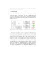
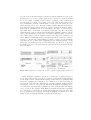
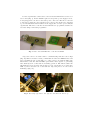
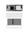
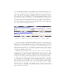
Flash Memory ‘Bumping’ Attacks
Sergei Skorobogatov
University of Cambridge, Computer Laboratory,
15 JJ Thomson Avenue, Cambridge CB3 0FD, United Kingdom
[email protected]
Abstract. This paper introduces a new class of optical fault injection
attacks called bumping attacks. These attacks are aimed at data extraction from secure embedded memory, which usually stores critical parts
of algorithms, sensitive data and cryptographic keys. As a security measure, read-back access to the memory is not implemented leaving only
authentication and verification options for integrity check. Verification is
usually performed on relatively large blocks of data, making brute force
searching infeasible. This paper evaluates memory verification and AES
authentication schemes used in secure microcontrollers and a highly secure FPGA. By attacking the security in three steps, the search space can
be reduced from infeasible > 2100 to affordable ≈ 215 guesses per block of
data. This progress was achieved by finding a way to preset certain bits
in the data path to a known state using optical bumping. Research into
positioning and timing dependency showed that Flash memory bumping
attacks are relatively easy to carry out.
Keywords: semi-invasive attacks, fault injection, optical probing
1
Introduction
Confidentiality and integrity of sensitive information stored in smartcards, secure microcontrollers and secure FPGAs is a major concern to both security
engineers and chip manufacturers. Therefore, sensitive data like passwords, encryption keys and confidential information is often stored in secure memory,
especially in Flash memory. This is mainly because data extraction from an embedded Flash memory is believed to be extremely tedious and expensive [1, 2]. In
addition, Flash memory offers re-programmability and partial updating, useful
for keeping firmware, keys and passwords up to date, and replacing compromised
ones. However, in some cases, the Flash memory is vulnerable to several types of
attacks. Sometimes the memory access path is the weakest link. In order to prevent unauthorised access to the memory, chip manufacturers widely use security
fuses and passwords in microcontrollers, FPGAs, smartcards and other secure
chips. This approach did not prove to be very effective against semi-invasive
attacks [3]. Furthermore, to make the protection more robust and to prevent
some known attacks on the security fuses, some chip manufacturers decided not
to implement direct access to internal data from the external programming and
debugging interfaces. That way, read access to the embedded memory was unavailable to the external interface and only the verify operation in a form of
comparison with uploaded data was left for data integrity check. Usually, such
verification is carried over large chunks of data in order to prevent brute force
attacks.
Optical fault injection attacks proved to be very effective against many protection schemes [4]. As these attacks require visibility of the chip surface without
the need of any mechanical contact, they should be classified as semi-invasive.
Backside approach can be used on modern sub-micron chips with multiple metal
layers that cover the surface and prevent direct access. Such an approach is simpler than the front-side as it does not require special chemicals for opening up
the chip package. Moreover, there is no danger of mechanical damage to the die
as the thick silicon substrate protects the active area. Mechanical milling is used
to open up the package followed by polishing of the silicon surface. Very cheap
engraving tools proved to be sufficient for that.
The results presented in this paper show that optical fault injection can be
successfully used to circumvent verify-only protection scheme in secure devices.
This technique was demonstrated on the Flash program memory of a “secure”
microcontroller and on the Flash array of a “highly secure” FPGA. However, it
can be applied to any device, that allows verification of the internal data against
uploaded one. The attack was carried out in three steps. The first step was aimed
at separating of the whole verification packet into blocks of data according to
the communication protocol. The second step, later called ‘bumping’, involved
splitting the data in each block into words corresponding to the width of the
data bus. The third step, later called ‘selective bumping’, was used to reduce
the number of guesses required to pass the verification within each word of data.
Using these techniques the data extraction time can be dramatically reduced to
hours and days compared with many years required for brute force attacks. As
these attacks do not require expensive equipment they can pose a big problem
to the hardware community. Without proper countermeasures in place security
in some devices could be easily compromised.
Another interesting direction of the research presented in this paper concerns
the possibility of AES key extraction using bumping attacks on the AES-based
authentication process. For that, a secure FPGA and a secure microcontroller
were tested. Both chips have hardware AES decryption engines for authentication and decryption of firmware updates. Research into positioning and timing
dependability of the bumping attacks was carried out. It was found that Flash
memory bumping attacks do not require precise positioning on the chip surface
and just reasonable timing precision, thus being also suitable for asynchronously
clocked chips. For selective bumping attacks some non-linear effects were observed where the sequence of bits set to a known state depended on the point of
fault injection.
This paper is organised as follows. Section 2 describes protection mechanisms
used in secure chips and background on the bumping attacks. Section 3 introduces experimental setup, while Section 4 shows the results. Section 5 discusses
limits and further improvements to these attacks. Some possible countermeasures
are presented in the concluding section.
2
Background
Target of my experiments was embedded Flash memory. It uses floating-gate
transistors to store the information [5]. Fig. 1 shows the overall structure of a
typical Flash memory, the layout of the memory cells and the details of the
floating-gate transistor operation modes. Data inside the Flash memory array
can only be accessed one row at a time, with the row itself being sent in smaller
chunks via read sense amplifiers. The number of the latter usually matches the
width of the data bus.
Fig. 1. Structure of Flash memory, layout of memory cells and modes of operation
High voltages are required to operate the Flash memory. Although they are
not necessary for reading the memory, the requirement for a special high-voltage
control logic and large charge pumps forces chip designers to place the Flash
memory separately from the rest of the chip logic. From a security point of view
this makes finding and attacking it easier. There are several places where the
attack could be targeted. One is the memory cells, but this way is not very
practical as it requires precise focusing and positioning not achievable with a
backside approach. Another place is the read sense amplifiers, however, in spite
of an easy way of locating and attacking them, the number of attack points increases with the width of data bus. Even for a narrow 8-bit data bus, mounting
eight lasers will be a non-trivial task. The same difficulties apply to the attack
point where the data bus itself is addressed. Contrary to the above mentioned
attack points, attacking the control logic that enables the output of the memory
array seems to be the most practical way as it requires only a single laser to
carry out the attack. Within the control logic itself there might be several vulnerable places ranging from reference current sources to the array and reference
voltages for the read sense amplifiers to the data latches and data bus output
control. From the implementation point of view, attacking voltage and current
sources could be easier both from the locating prospective and laser injection.
There are some references to previous attacks carried out on old smartcards with
external programming voltage Vpp [6]. A similar effect can be achieved with a
laser interfering with the operation of the internal high-voltage supply.
In order to implement optical fault-injection attacks, the chip surface needs
to be accessible. This can be done from both front and rear sides. Modern chips
have multiple metal layers obstructing the view and preventing optical attacks.
Therefore, the only practical way of implementing optical fault injection on chips
fabricated with 0.35 µm or smaller technology is from their rear side. Silicon is
transparent to infrared light with wavelengths above 1000 nm, thus making it
possible to observe the internal structure of the chip with non-filtered CCD cameras. Optical fault injection can be carried out using inexpensive infrared laser
diodes. The effective frequency at which lasers can inject signals inside operating
chips is limited to several megahertz, as free carriers created by photons require
some time for recombination. Therefore, although lasers offer a relatively inexpensive way of controlling internal signals, they are not as effective for direct
signal injection as microprobing techniques [7]. One important thing to know is
that for Flash memory, optical fault injection causes either ‘0’ to ‘1’ or ‘1’ to
‘0’ state changes, depending on the location of injection, but never both at the
same time.
Older microcontrollers had a security protection fuse. Once activated it disabled access to the on-chip memory. This has proved to be not very secure as
such fuses are relatively easy to locate and disable using various attacks. Semiinvasive attacks made security-fuse disabling even easier [3]. As a precaution, chip
manufacturers started abandoning readback access to the embedded memory by
implementing verify-only approach. In this case the content of memory was compared with uploaded data and a single-bit response in the form of pass/fail was
sent back. So far this helped a lot, especially when the length of verified blocks
was long enough to prevent brute force searching. Moving from 8-bit data bus
to 16-bit and later to 32-bit helped in keeping exhaustive searching attacks even
further away. All these steps, provided there are no errors in the design, improve
security. The verification process can take place both in hardware or in software.
It is impossible to verify the whole memory in one go, so the process is split
into blocks with their size limited by the available SRAM buffer or hardware
register. The result of the verification is either available immediately on the first
incorrect block, or it can be checked in a status register, or rarely available only
at the end of the whole memory check.
Fig. 2 illustrates an example of a typical secure verify-only implementation.
Very often the result of the verify operation is known only at the end. However, due to the limited size of buffers and registers, smaller blocks of data are
verified with the result accumulated inside the chip. The division into blocks
can usually be observed on the data transfer protocol or via eavesdropping on
the communication line. That way the device under test can be put into a mode
where it discloses the result of the verification operation for each block. However,
for some devices, the intermediate verification result is available as a part of the
standard protocol or can be easily requested. It becomes more complicated when
the block consists of multiple words of data, for example, if the verification is
performed after receiving every packet of 16 bytes. Still, as the verification is
done in hardware, memory contents must be read before the values are compared and this is done via a data bus of limited width. This way there will be
some inevitable delay between each word of data read from the memory. Hence,
with a fast enough fault injection one can influence the value of each word of the
data. This will be an example of a bumping attack (Fig. 2b). More interesting
results should be expected if the data latching time is slightly changed or if the
value of data is influenced on its way to the latches. This is possible because the
bits of data cannot reach the registers exactly at the same time. If this process
can be influenced with fault injection attacks it may allow certain bits of data to
be kept to a known state, thus making it possible to brute force the remaining
bits. There are two possible ways of applying selective bumping attacks – on the
rising edge of the fault injection or on the falling (Fig. 2b). However, both events
should happen close to the time when the data from memory is latched into the
data bus drivers.
Fig. 2. Timing diagram of a verify-only operation: (a)data blocks, (b)data words level
Term ‘bumping’ originally comes from a certain type of physical attack on
door locks [8]. The idea is to force the key bits into a desired state which will allow
access. In the context of the hardware security of semiconductors, ‘bumping’ shall
mean here bypassing the verification of a certain block of data by forcing the
data bus into a known state. Alternatively, ‘selective bumping’ shall mean that
certain bits of data are forced into known states allowing the remaining bits to
be searched through all possible combinations. Some parallels with lock bumping
can be observed. For example, Flash memory bumping attacks allow bypassing
the verification for certain words of data without knowing their real value. The
more powerful selective bumping attack allows masking of certain bits of data
within each word thus substantially reducing the attack time.
3
Experimental Method
There are not many microcontrollers that lack readback access, as this complicates their programming algorithm and many chip manufacturers found this
security feature excessive. However, some recent microcontrollers, marketed as
“secure”, benefit from verify-only feature, as well as AES authentication and
SHA-1 integrity check for the firmware. On the other hand, recent non-volatile
FPGA chips use a verify-only approach in the high-end security market. Such
chips are also marketed as “highly secure”.
For my first set of experiments I chose a secure low-end 8-bit microcontroller,
the NEC 78K/0S µPD78F9116 with 16 kB of embedded Flash [9]. The chip is
fabricated in 0.35 µm and has 3 metal layers. The on-chip firmware bootloader
allows the following memory access commands to be executed via SPI, IIC or
UART interfaces: Erase, Pre-Write, Write, Verify and Blank check [10]. Only the
‘Verify’ command seems useful for attempts of data extraction.
My next set of experiments was carried out on a so-called highly secure Flash
FPGA, the Actel ProASIC3 A3P250 [11]. Fabricated with a 0.13 µm process
with 7 metal layers, this chip incorporates 1,913,600 bits of bitstream configuration data. According to the manufacturer’s documentation on this chip: “Even
without any security measures, it is not possible to read back the programming
data from a programmed device. Upon programming completion, the programming algorithm will reload the programming data into the device. The device will
then use built-in circuitry to determine if it was programmed correctly”. More
information on the programming specification can be obtained indirectly from a
programming file which is usually in STAPL format [12]. Alternatively, all the
necessary information can be obtained by eavesdropping on the JTAG interface
during device programming. The analysis of a simple programming file revealed
the following operations on embedded Flash array: Erase, Program and Verify.
Again, only the ‘Verify’ operation can access the internal configuration. Apart
from the Flash Array, this FPGA has an AES hardware decryption engine with
authentication for firmware updates. As the AES key is stored in Flash memory,
it was also evaluated against bumping attacks.
For a detailed demonstration of the bumping attacks I used an engineering
sample of a secure microcontroller with AES authentication of the firmware. It
was provided by an industrial collaborator under a non-disclosure agreement
and is therefore not identified here. This microcontroller has non-volatile programmable memory for an AES key and other security features. As the memory
had an independent power supply pin I was able to carry out bumping attacks
using non-invasive power glitching. On one hand, it simplified the setup, on the
other, it allowed better timing accuracy for characterisation.
Opening up the first two chips was not a difficult task, since only the backside
access was a suitable option. No chemicals are required for opening up chips from
the rear side. The plastic can be milled away with low-cost hobbyist engraving
tools available from DIY shops. The copper heatsink, often attached to the
die, can be removed with a knife, followed by removing the glue underneath
mechanically and finally cleaning the die with a solvent.
For the experiments both the microcontroller and the FPGA were soldered on
test boards (Fig. 3). As the FPGA requires four separate power supply sources,
it was plugged into another board with power connectors. The microcontroller
board was receiving its power supply from a control board. Both test boards had
a power-measurement 10 Ω resistor in the supply line for later power analysis
experiments. The microcontroller and the FPGA were programmed with some
test data using a universal programmer.
Fig. 3. Test boards with NEC microcontroller and FPGA
A special control board was built for communicating with the tested chips
(Fig. 4a). This board was receiving commands from a PC via UART interface and
was controlling the test boards. The core of the control board was the Microchip
PIC24 microcontroller with 40 MIPS performance thus capable of generating
laser fault injection events with 25 ns timing precision. The infrared 1065 nm
100 mW laser diode module was mounted on an optical microscope with 20×
NIR objectives and the test board with the chip was placed on a motorised
XYZ-stage (Fig. 4b).
Fig. 4. Test setup: (a)control board, (b)test board under the microscope
The experiments started with finding the minimum length of block verification and possibility of obtaining any intermediate results. Then optical fault
injection attacks were used to reduce the verification length down to a single
word of the data bus. In this way the width of the data bus can be determined.
Alternatively, the width of the data bus can be determined by counting the
number of read sense amplifiers under a microscope. As a preliminary step for
optical fault injection, laser scanning was performed. This can significantly reduce the area of search for successful fault injection. Also, some power analysis
measurements [13] were made using a digital storage oscilloscope to estimate
the internal timings of the verification process. This can assist in carrying out
selective bumping attacks later, thereby saving the time otherwise required for
exhaustive search.
4
Results
Initial experiments were aimed at finding places sensitive to optical fault injection. For that, both chips were exposed to laser scanning imaging, also called
OBIC imaging [14]. The same setup as for optical fault injection was used, with
the difference being that the photo-current produced by the laser’s photons was
registered with a digital multimeter. The result of the laser scan is presented in
Fig. 5 and allows identification of all major areas. Flash arrays are quite large
and easily identifiable structures on a chip die. However, for bumping attacks
of more interest is the memory control logic. As that is usually placed next to
the array, obvious places for exhaustive search are located nearby. The area for
search is designated in Fig. 5 as ‘Flash control’. For the NEC microcontroller,
many places within the control area were sensitive to optical bumping causing
the memory to change its state to all ‘0’ when the laser was switched on for
the whole verification process. For the FPGA, an exhaustive search for areas
sensitive to bumping was made across the whole chip with a 20 µm grid and the
result is presented in Fig. 6a. Each point was verified against the correct initial
value and against all ‘1’. White areas represent successful bumping with all bits
set to ‘1’, black areas correspond to faulty verification, while grey area represent
no change. Surprisingly, no success was achieved when AES authentication was
targeted in the FPGA (Fig. 6b). Only faulty authentications were received for a
small area which are of no use since the attacker has no means of observing the
result of AES decryption, so he cannot mount differential fault attacks [15]. This
could be the result of abandoning read sense amplifiers in the Flash memory that
stores the AES key and using direct Flash switches instead, or it could be that
some countermeasures against optical fault injection attacks were in place.
Further experiments were aimed at splitting the full verification process into
blocks of data. The NEC microcontroller has 16384 bytes of internal memory.
According to the Flash memory write application note [10], each verification
command receives 128 bytes of data via the serial programming interface before
starting the verification process. However, the status register is not updated
with the result until all 16384 bytes of data are received and verified. That
Fig. 5. Laser scanning images: (a)NEC microcontroller, (b)FPGA
means there is no simple non-invasive way of splitting up the data sequence.
However, the fact that each verification is run on 128-bytes blocks means that it
is fairly easy to apply a bumping attack for the duration of the verify operation
on all blocks except the chosen one. For the Actel FPGA, splitting 1,913,600
bits of the verification data into 832-bit blocks came from the analysis of both
the STAPL programming file and the JTAG communication protocol. These 832
bits of data are sent as 32 packets of 26 bits, however, the verification is done on
all 832 bits simultaneously in hardware. Moreover, the result of the verification
is available after each 832-bit block, making further analysis easier compared to
the above microcontroller, as there is no need to do bumping on other blocks.
Fig. 6. Fault injection sensitivity mapping: (a)Verify Array operation, (b)AES authentication operation
The next step was aimed at splitting the verification blocks into words down
to the width of the memory data bus. Power analysis measurements were carried
out on both chips revealing the exact timing for the internal verification process
in the form of higher power consumption (Fig. 7). For easier observation, a
10× zoom is presented at the bottom. Block verification takes 16.4 ms for the
microcontroller and only 40 µs for the FPGA. Moreover, for the microcontroller
128 peaks in the power consumption are clearly distinguishable making it clear
that 8 bits are verified at a time (Fig. 7a). For the FPGA, the granularity of
the verification process was invisible in the power trace. However, the number of
read sense amplifiers observed under a microscope suggested that the memory
data bus is 32 bits wide resulting in 1.5 µs verification time per word. This was
later confirmed with bumping experiments.
Fig. 7. Power analysis on block verification: (a)NEC microcontroller, (b)FPGA
It was not possible to distinguish any difference between correct and incorrect
words of data in the power trace because the signal was too noisy. Averaging
might help, but will substantially increase the attack time making it not practical. Therefore, on its own, power analysis was not useful for breaking into the
Flash of these chips. However, it gave important information about the timing
of the internal verification process which was useful for carrying out bumping
and selective bumping attacks later.
Bumping attack to separate words of data on the microcontroller was straightforward as it uses an external clock signal. That way the attack can be easily
synchronised to the chips operations. It takes 128 µs to verify each word of data
by the internal firmware of the microcontroller. Hence, in order to turn certain
bytes into a known zero state the laser should be turned on during that time.
The process was trickier for the FPGA. It runs on its internal clock, which is
not very stable and was changing over time. It takes only 1.5 µs to verify each
word of data for the on-chip hardware of the FPGA. However, timing control
with sub-microsecond precision is not a problem for the laser. The bumping
attack aimed at the separation of the words of data within the block worked
reliably even for the internally clocked FPGA. As the clock jitter was less than
2%, there was no overlapping between verifications of each word, since there
were only 26 words per block.
The last step was aimed at implementing the selective bumping attacks. Triggering the laser pulse at the precise time for data latching in the microcontroller
was achieved without much trouble. However, there was no large improvement
compared to the standard bumping attack – only reduction of the search field
from 28 to 25 per byte in the block, totalling 212 attempts per whole block. One
important thing to know is that for each attempt the full verification process
must be run and it takes at least five seconds to get the result of the verification
at the end. Hence, selective bumping will improve the full data extraction time
from four months to two weeks. Applying the selective bumping attack to the
FPGA was much more difficult due to the lack of synchronisation. Therefore,
the probability of hitting the data latching at a particular time was reduced by
a factor of the data bus width. However, this was not the only obstacle for the
selective bumping. It turned out that some bits within the 32-bit word have very
close timing characteristics, so it was extremely hard to separate them reliably.
Fortunately, as mentioned earlier, there are many points on the chip where the
bumping attacks can be applied. By testing different points, I found that some of
them offer better separation of bits in time. Selective bumping does not require
knowledge about the sequence of bits as this information can be easily obtained
during the experiment. Since the all-‘1’ state always pass the verification, the
next attempt involves selective bumping into 32 possible combinations with a
single ‘0’ bit. Then followed by 31 combinations of two ‘0’ bits, and so on until
the whole word is recovered. The best case has required only 213 attempts per recovery of the word value, totalling 218 searches per 832-bit block. This is slightly
more than the theoretically predicted 28 per word and 213 per block because of
the jitter caused by the internally clocked hardware of the chip. Although each
block can be verified independently, it cannot be addressed separately. That
means it takes longer to verify higher blocks, on average 10 ms. That way the
whole configuration bitstream can be extracted in about one month. Without
the use of selective bumping attacks, that is with only bumping attacks, such
extraction would take more than fifty thousand years. This is a far more significant improvement than with the microcontroller. However, this was expected
for 16-bit and 32-bit chips, which no longer could be brute forced through all
possible values within reasonable time.
The final set of experiments was carried out on a secure microcontroller with
AES authentication. As the chip under test was not in production at the time
of testing, the details of the setup are omitted. Only the statistical results for
optical bumping attacks are presented. However, this experiment shows how the
selective bumping helps in dramatic reduction of the search field.
Since the chip has a sophisticated secure AES key programming method,
it was supplied pre-programmed by the industrial collaborator. Authentication
required a special high-speed hardware setup that was also provided. Therefore,
my work was limited to finding a way of forcing the chip into bumping and
selective bumping and this was achieved by means of just non-invasive power
supply glitching attacks. The bumping caused certain bits of key to change to
‘1’. The result of the authentication was either pass or fail. Further analysis
revealed that the key was transferred from the internal secure memory in 8
words, which means the memory bus is 16-bit wide. The probability of bumping
depended from the time of glitching with low probability suggesting the time for
selective bumping (Fig. 8a).
Fig. 8. Attacking AES authentication: (a)bumping, (b)selective bumping
The result of the selective bumping attack is presented in Fig. 8b showing
which bits are changing at a particular time of glitching for one word. It is
clear that the bits are well separated in time thus allowing easy key recovery.
Although the bumping attack was enough to extract the whole key in about
one week, since each word was only 16-bit wide, selective bumping brought this
figure down to a few minutes.
5
Implications and Further Improvements
The above results were achieved on two microcontrollers and one FPGA. It
would be interesting to compare the results with other chips. However, it is
not easy to find candidates since most microcontrollers do have readback access
through programming or debugging interface. However, when it comes to the
AES authentication and hash functions, there might be many chips which store
keys in Flash memory. In the FPGA industry, very few manufacturers offer nonvolatile chips. The bumping attacks could also be compared with another sample
of the same chip, to see if the sequence of bits masked by selective bumping
remains the same.
In order to improve the speed of the bumping attacks, a more efficient algorithm could be used. For example, an exhaustive timing analysis could be
applied to the first block of data. That way, selective bumping would give faster
results for the following blocks.
One can argue that power analysis might give a better result as it was used
to break many security protection schemes. However, applying power analysis to
the verification process will require too many power traces to be acquired and
analysed. This will inevitably lead to a very long extraction time, not practical
for a real attack. However, this might work if only a few bytes of data would
have to be extracted, for example, a password or an encryption key.
I noticed that FPGA security relies heavily on obscurity. That ranges from
the lack of any documentation on the JTAG access interface, and absence of
information on the internal operations, down to the data formats. This works well
unless an attacker is that determined to find all this information on their own. My
experiments showed how some information can be found via systematic testing
of device operations. That way, for example, I found the correspondence between
bits in the 832-bit verification data and bits in the data bus. Alternatively, for
some chips more information can be gained through analysis of development
tools and programming files.
On the security of Flash FPGA, one can argue that the demonstrated attack
will not entirely compromise its security. This is because on top of the verify-only
access control there are other security protection mechanisms, such as FlashLock
access control and AES bitstream encryption with proprietary integrity-check algorithm [15]. This is true, but the fact that verify-only schemes do not provide
the level of protection anticipated by the manufacturer should cause concern,
especially as there might be the possibility of failures in other protection mechanisms. Furthermore, some users were relying solely on the fact that there was
no readback capability in the FPGAs.
Bumping attacks demonstrated in this paper used only one parameter – time.
It might be possible to find two independent parameters, for example, time and
laser power, or time and positioning. That way, more powerful 2D bumping
attacks could be implemented.
6
Conclusion
Two types of bumping attacks were introduced – bumping and selective bumping. The first is aimed at bypassing the verification of a block, while the other
is aimed at presetting certain bits of data inside the block. Successful attacks
on a microcontroller with secure memory verification, on an FPGA with secure
firmware verification and on a secure microcontroller with AES authentication
were presented. Verify-only memory protection scheme is used in some chips as
a more secure alternative to access protection fuses.
The attack was carried out in three steps. The first step was aimed at separating the process into blocks. The second step involved splitting the data in
each block into words corresponding to the width of the data bus. The third
step was used to reduce the number of guesses required to pass the verification
within each word of data. Although for the 8-bit bus selective bumping was not
very useful, only a reduction from 28 to 25 searches, for the 32-bit bus selective
bumping attack allowed a tremendous reduction from 232 to just 213 searches,
which makes it practical. This is very important as the width of data bus in
modern devices is more often 16 or 32 bits rather than 8 bits as in old microcontrollers. The attack was possible because each individual bit within a word
has different sensitivity to fault injection thus allowing reliable separation from
the others.
My research proved that a verify-only approach does not work on its own.
Even from a so-called highly secure FPGA the configuration can be extracted
using bumping attacks. Fortunately, this is not the only protection that is available in Actel FPGAs. In addition to the verify-only scheme, the FlashLock can
be activated or even more robust AES bitstream encryption with proprietary
integrity check algorithm. The latter prevents verification on arbitrary data [16].
Nevertheless, manufacturer’s claims that data extraction from these FPGAs is
not possible is no longer true. Although the FPGA was developed with some
security in mind and has independent clocking and a reasonably wide data bus,
it was still possible to successfully apply bumping attacks and get significant
improvements over brute force attacks.
My experiments showed that bumping attacks are easy to apply even on
chips clocked from an internal asynchronous source. My attempts of applying
conventional power analysis to distinguish a single-bit change in the Hamming
weight of data were unsuccessful. However, the results from the power analysis
were useful for optimising the timing of bumping attacks. Using selective bumping technique the data extraction time can be dramatically reduced to hours
and days compared with many years required for brute-force searching. As these
attacks do not require expensive equipment they can pose a big problem to the
hardware community. As protection against bumping attacks, similar techniques
can be used as for other types of optical fault injection attacks. For example,
light sensors might prevent optical attacks, while a robust verification process
could make bumping attacks very difficult to use. Alternatively, a very long verification process could make finding of each bit not very practical. In addition,
clock jitters and dummy cycles would make bumping much harder to synchronise. Secure Flash memory design could also prevent bumping as it was shown
on the secure Flash memory storing AES key in the FPGA.
Bumping attacks can find their way in partial reverse engineering of the internal chip structure and its operation. For example, data scrambling in the
configuration bitstream of the FPGA could be found using bumping attacks.
Flash memory bumping attacks do not require precise positioning on the chip
surface and just reasonable timing precision, hence, easily applied. Flash memory
bumping attacks complement other semi-invasive methods, such as optical probing [4], laser scanning [14] and optical emission analysis [17]. However, bumping
gives the result faster and does not require stopping the clock frequency or placing the device in an idle state which sometimes is not feasible. Once again,
semi-invasive attacks such as optical fault injection proved their effectiveness for
deep sub-micron chips which should be of concern to secure chip manufacturers.
Very likely this will result in the introduction of new countermeasures during
the design of semiconductor chips.
References
1. Xilinx CoolRunner-II CPLDs in Secure Applications. White Paper http://www.
xilinx.com/support/documentation/white_papers/wp170.pdf
2. Design Security in Nonvolatile Flash and Antifuse FPGAs. Security Backgrounder
http://www.actel.com/documents/DesignSecurity_WP.pdf
3. Skorobogatov, S.: Semi-invasive attacks - A new approach to hardware security analysis. Technical Report UCAM-CL-TR-630, University of Cambridge,
Computer Laboratory, April 2005 http://www.cl.cam.ac.uk/techreports/
UCAM-CL-TR-630.pdf
4. Skorobogatov, S., Anderson, R.: Optical Fault Induction Attacks. Cryptographic
Hardware and Embedded Systems Workshop (CHES-2002), LNCS 2523, pp. 2-12
5. Brown, W.D., Brewer, J.E.: Nonvolatile semiconductor memory technology: a comprehensive guide to understanding and using NVSM devices. IEEE Press, 1997
6. Anderson, R.J., Kuhn, M.G.: Tamper resistance - a cautionary note. The Second
USENIX Workshop on Electronic Commerce, Oakland, California, November 1996
7. Wagner, L.C.: Failure Analysis of Integrated Circuits: Tools and Techniques. Kluwer
Academic Publishers, 1999
8. Tobias, M.W.: Opening locks by bumping in five seconds or less: is it really a threat
to physical security? A technical analysis of the issues, Investigative Law Offices
http://podcasts.aolcdn.com/engadget/videos/lockdown/bumping_040206.pdf
9. NEC PD789104A, 789114A, 789124A, 789134A Subseries User’s Manual. 8Bit Single-Chip Microcontrollers http://www2.renesas.com/maps_download/pdf/
U13037EJ1V0PM00.pdf
10. NEC 78K/0, 78K/0S Series 8-Bit Single-Chip Microcontrollers. Flash Memory
Write. Application Note http://www.necel.com/nesdis/image/U14458EJ1V0AN00.
pdf
11. Actel ProASIC3 Handbook. ProASIC3 Flash Family FPGAs http://www.actel.
com/documents/PA3_HB.pdf
12. Actel: ISP and STAPL. Application Note AC171 http://www.actel.com/
documents/ISP_STAPL_AN.pdf
13. Kocher, P., Jaffe, J., Jun, B.: Differential Power Analysis. CRYPTO99, LNCS, vol.
1666, Springer-Verlag, 1999, pp. 388-397
14. Ajluni, C.: Two new imaging techniques promise to improve IC defect identification. Electronic Design, Vol. 43(14), July 1995, pp. 37–38
15. Giraud, C.: DFA on AES. H. Dobbertin, V. Rijmen, A. Sowa (Eds.): AES 2004,
LNCS 3373, 2005, pp. 2741
16. Actel ProASIC3/E Production FPGAs. Features and Advantages http://www.
actel.com/documents/PA3_E_Tech_WP.pdf
17. Skorobogatov, S.: Using Optical Emission Analysis for Estimating Contribution to
Power Analysis. 6th Workshop on Fault Diagnosis and Tolerance in Cryptography
(FDTC 2009), September 2009, Lausanne, Switzerland. IEEE-CS Press, ISBN 9780-7695-3824-2, pp.111-119