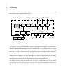
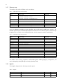
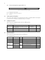
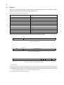
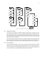
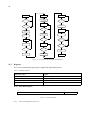
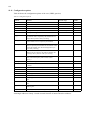
1
LEON3 GR-XC3S-1500 Template Design
Based on GRLIB, October 2006
Jiri Gaisler, Marko Isomäki
Copyright Gaisler Research, 2006.
2
1
Introduction
1.1
Scope
This document describes a LEON3 template design customized for the GR-XC3S-1500 FPGA development board. The template design is intended to familiarize users with the LEON3 processor and the
GRLIP IP library.
1.2
Requirements
The following hardware and software components are required in order to use and implement the GRXC3S-1500 LEON3 template design:
•
GRLIB IP Library 1.0.8
•
PC work station with Linux or Windows 2000/XP with Cygwin
•
GR-XC3S-1500 board with JTAG programming cable
•
Xilinx ISE 7.1.04i Development software (WebPack or Regular Edition)
•
Synplicity Synplify 8.4 or higher (optional).
For LEON3 software development, the following tools are recommended
1.3
•
BCC Bare-C LEON Cross-compiler 1.0.24
•
RCC RTEMS ERC32/LEON Cross-compiler system 1.0.12
GR-XC3S-1500 board
The GR-XC3S-1500 board is developed by Pender Electronic Design (CH), and provides a flexible
and low-cost prototype platform for LEON systems. The GR-XC3S-1500 board has the following
features:
•
Xilinx Spartan3 XC3S-1500-4 FPGA
•
8 Mbyte flash prom (8Mx8) and 64 Mbyte SDRAM (16Mx32)
•
Two RS-232 interfaces
•
USB-2.0 PHY
•
10/100 Mbit/s ethernet PHY
•
Two PS/2 interfaces
•
VGA video DAC and 15-pin connector
•
JTAG interface for programming and debug
•
4x20 pin expansion connectors
3
GR-XC3S-1500 Development Board
1.4
Reference documents
The LEON3 template design is based on GRLIB, and uses the GRLIP AMBA plug&play configuration method. The following manuals should therefore be carefully studied in order to understand the
design concept:
•
GRLIB User’s Manual 1.0.8
•
AMBA Specification 2.0
•
GRLIB IP Core’s Manual
4
2
Architecture
2.1
Overview
The LEON3 GR-XC3S-1500 template design consists of the LEON3 processor and a set of IP cores
connected through the AMBA AHB/APB buses.
RS232
JTAG
PHY
3x LVDS
2x CAN
Serial
Dbg Link
JTAG
Dbg Link
Ethernet
MAC
SpaceWire
Links
Multi-core
CAN-2.0
Spartan3-1500 FPGA
DSU3
LEON3
Processor
AMBA AHB
AHB
Controller
Memory
Controller
AMBA APB
AHB/APB
Bridge
VGA
PS/2
UART
Timers
Video
DAC
PS/2 IF
RS232
WDOG
IrqCtrl
I/O port
8/32-bits memory bus
PROM
I/O
SDRAM
16-bit I/O port
Figure 1. LEON3 template design block diagram
The design is centered around the AMBA Advanced High-Speed bus (AHB), to which the LEON3
processor and other high-bandwidth devices are connected. External memory is accessed through a
combined PROM/IO/SRAM/SDRAM memory controller. The on-chip peripheral devices include
three SpaceWire links, ethernet 10/100 Mbit MAC, dual CAN-2.0 interface, serial and JTAG debug
interfaces, two UARTs, interrupt controller, timers and an I/O port. The design is highly configurable,
and the various features can be suppressed if desired.
Most parts of the design is provided in source code under the GNU GPL license. The exception is the
floating-point unit (GRFPU-Lite) and the SpaceWire core, which are only available under a commercial license. For evaluation and prototyping, suitable netlists for the GR-XC3S-1500 board are provided. The netlists will automatically be included in the design during place&route.
The LEON3 processors and associated IP cores also exist in a fault-tolerant (FT) version. The FT
cores detects and removes SEU errors due to cosmic radiation, and are particularly suitable for systems that operate in the space environment. The FT version of LEON3 and GRLIB is only licensed
commercially, please contact Gaisler Research for further details.
5
2.2
LEON3 SPARC V8 processor
The template design is based the LEON3 SPARC V8 processor. The processor core can be extensively
configured through the xconfig graphical configuration program. In the default configuration, the
cache system consists or 8 + 4 Kbyte I/D cache with cache snooping enabled. The LEON3 debug support unit (DSU3) is also enabled by default, allowing downloading and debugging of programs
through a serial port or JTAG.
3-Port Register File
Trace Buffer
IEEE-754 FPU
Co-Processor
7-Stage
Integer pipeline
HW MUL/DIV
Local IRAM
I-Cache
Debug port
Debug support unit
Interrupt port
Interrupt controller
Local DRAM
D-Cache
I/D MMU
AHB I/F
AMBA AHB Master (32-bit)
Figure 2. LEON3 processor core block diagram
2.3
Memory interfaces
The external memory is interfaced through a combined PROM/IO/SRAM/SDRAM memory controller core (MCTRL). The GR-XC3S-1500 board provides 8 Mbyte flash PROM and 64 Mbyte
SDRAM, and the SRAM and I/O signals are available on the extension connectors.
APB
A
AHB
ROMSN[1:0]
OEN
WRITEN
CS
OE
WE
IOSN
CS
OE
WE
MEMORY
PROM
D
A
D
I/O
A
SRAM
A
D
CONTROLLER
RAMSN[4:0]
RAMOEN[4:0]
RWEN[3:0]
MBEN[3:0]
SDCLK
SDCSN[1:0]
SDRASN
SDCASN
SDWEN
SDDQM[3:0]
CS
OE
WE
MBEN
CLK
CSN
RAS
CAS
WE
DQM
D
A[16:15]
BA
SDRAM
A
A[14:2]
D
A[27:0]
D[31:0]
Figure 3. PROM/IO/SRAM/SDRAM Memory controller
2.4
AHB status register
The AHB status register captures error responses on the AHB bus, and lock the failed address and
active master. These values allows the software to recover from error events in the system.
6
2.5
SpaceWire links
The template design can be configured with up to three SpaceWire links. Each link is controlled separately through the APB bus, and transfers received and transmitted data through DMA transfer on
AHB. The SpaceWire links can also optionally be configured with RMAP support in hardware.
2.6
Timer unit
The timer unit consists of a common scaler and up to 7 individual timers. The timers can work in periodical or on-shot mode. One of the timers can optionally be configured as a watchdog.
2.7
Interrupt controller
The interrupt controller handles up to 15 interrupts in two priority levels. The interrupt are automatically assigned and routed to the controller through the use of the GRLIB plug&play system.
2.8
UART
One or two UARTs can be configured in the design. The UART have configurable FIFO sizes, and
have separate baud rate generators.
2.9
General purpose I/O port
A general purpose I/O port (GPIO) is provided in the design. The port can be 1 - 32 bits wide, and
each bit can be dynamically configured as input or output. The GPIO can also generate interrupts
from external devices.
2.10
Ethernet
An ethernet MAC can be enabled. The MAC supports 10/100 Mbit operation is half-or full duplex.
An ethernet based debug interface (EDCL) can optionally also be enabled.
2.11
CAN-2.0
One or two CAN-2.0 interfaces can be enabled. This interface is based on the CAN core from Opencores, with some additional improvements.
2.12
VGA controller
A text-based video controller can optionally be enabled. The controller can display a 80x48 character
screen on a 640x480 monitor.
2.13
PS/2 keyboard interface
A PS/2 keyboard interface can optionally be enabled. It provides the scan codes from a regular keyboard, and has a 16 byte FIFO.
2.14
Clock generator
The portable clock generator core is used to generate the processor and synchronized SDRAM clock.
The clock generator can generate an arbitrary frequency by multiplying and dividing the 50 MHz
board clock. The clock scaling factor is configurable through the xconfig tool.
7
2.15
GRLIB IP Cores
The design is based on the IP cores from the GRLIB IP library shown in table 1.
Table 1. Used IP cores
2.16
Core
Function
Vendor
Device
LEON3
LEON3 SPARC V8 32-bit processor
0x01
0x003
DSU3
LEON3 Debug support unit
0x01
0x004
IRQMP
LEON3 Interrupt controller
0x01
0x00D
APBCTRL
AHB/APB Bridge
0x01
0x006
MCTRL
32-bit PROM/SRAM/SDRAM controller
0x04
0x00F
AHBSTAT
AHB failing address register
0x01
0x052
AHBUART
Serial/AHB debug interface
0x01
0x007
AHBJTAG
JTAG/AHB debug interface
0x01
0x01C
APBUART
8-bit UART with FIFO
0x01
0x00C
GPTIMER
Modular timer unit with watchdog
0x01
0x011
GRGPIO
General purpose I/O port
0x01
0x01A
GRSPW
SpaceWire link
0x01
0x01F
ETH_OC
10/100 Mbit/s Ethernet MAC
0x01
0x01D
CAN_MC
Multi-core CAN 2.0 interface
0x01
0x019
APBPS2
PS/2 Mouse/Keyboard interface
0x01
0x060
APBVGA
Text-based VGA controller
0x01
0x061
Interrupts
The following table indicates the interrupt assignment:
Table 2. Interrupt assignment
Core
Interrupt
APBUART1
2
APBUART2
3
APBPS2
5
AHBSTAT
7
GPTIMER
8, 9
GRSPW 1, 2, 3
10, 11, 12
ETH_OC
12
CAN
13, 14
See the manual of the respective core for how and when the interrupts are raised. All interrupts are
forwarded to the LEON3 processor, through the IRQMP interrupt controller.
8
2.17
Memory map
The memory map of the AHB bus can be seen below:
Table 3. AHB address range and bus indexes
Core
Address range
Bus Index
MCTRL
0x00000000 - 0x20000000 : PROM area
0
0x20000000 - 0x40000000 : I/O area
0x40000000 - 0x80000000 : SRAM/SDRAM area
APBCTRL
0x80000000 - 0x81000000 : APB bridge
1
DSU3
0x90000000 - 0xA0000000 : Registers
2
ETH_OC
0xFFFB0000 - 0xFFFB1000 : Registers
5
CAN_MC
0xFFFC0000 - 0xFFFC1000 : Registers
4
AHB plug&play
0xFFFFF000 - 0xFFFFFFFF : Registers
-
Access to addresses outside the ranges described above will return an AHB error response. The
detailed register layout is defined in the manual for each IP core. The control registers of most on-chip
peripherals are accessible via the AHB/APB bridge, which is mapped at address 0x80000000.
Table 4. APB address range and bus indexes
Core
Address range
Bus Index
MCTRL
0x80000000 - 0x80000100
0
APBUART
0x80000100 - 0x80000200
1
IRQMP
0x80000200 - 0x80000300
2
GPTIMER
0x80000300 - 0x80000400
3
APBPS2
0x80000500 - 0x80000600
5
APBVGA
0x80000600 - 0x80000700
6
AHBUART
0x80000700 - 0x80000800
7
GRGPIO
0x80000800 - 0x80000900
8
GRSPW 1
0x80000A00 - 0x80000B00
12
GRSPW 2
0x80000B00 - 0x80000C00
13
GRSPW 3
0x80000D00 - 0x80000E00
14
AHBSTAT
0x80000F00 - 0x80001000
15
APB plug&play
0x800FF000 - 0x80100000
-
The address of the on-chip peripherals is defined through the AMBA plug&play configuration, and
can be changed by editing the top level design (leon3mp.vhd).
2.18
Signals
The template design has the following external signals.
Table 5. Signals
Name
Usage
Direction
Polarity
CLK
Main system clock (50 MHz)
In
-
CLK3
Ethernet clock (25 MHz)
In
-
9
Table 5. Signals
Name
Usage
Direction
Polarity
RESETN
System reset
In
Low
PLLREF
Feedback for SDRAM clock generation
In
-
ERRORN
Processor error mode indicator
Out
Low
ADDRESS[21:2]
Memory word address
Out
High
DATA[31:0]
Memory data bus
BiDir
High
RAMSN[3:0]
SRAM chip selects
Out
Low
RAMOEN[3:0]
SRAM output enable
Out
Low
RWEN[3:0]
SRAM write enable strobe
Out
Low
OEN
Output enable
Out
Low
WRITEN
Write strobe
Out
Low
BRDYN
Bus ready
In
Low
ROMSN[1:0]
PROM chip select
Out
Low
IOSN
I/O area chip select
Out
Low
READ
Read cycle indicator
Out
High
SDCLK
SDRAM Clock
Out
-
SDCSN[1:0]
SDRAM chip select
Out
Low
SDWEN
SDRAM write enable
Out
Low
SDRASN
SDRAM row address select
Out
Low
SDCASN
SDRAM column address select
Out
Low
SDDQM[3:0]
SDRAM Data qualifier
Out
Low
DSUEN
DSU Enable
In
High
DSUBRE
DSU Break
In
High
DSUACT
DSU Active
Out
High
TXD1
UART transmit data
Out
Low
RXD1
UART 1 receive data
In
Low
RTSN1
UART 1 ready to send
Out
Low
CTSN1
UART 1 clear to send
In
Low
TXD2
UART 2 transmit data
Out
Low
RXD2
UART 2 receive data
In
Low
RTSN2
UART 2 ready to send
Out
Low
CTSN2
UART 2 clear to send
In
Low
PIO[15:0]
General purpose I/O port
BiDir
High
TCK
JTAG clock
In
High
TMS
JTAG strobe
In
High
TDI
JTAG data in
In
High
TDO
JTAG data out
Out
High
10
Table 6. SpaceWire signals
Name
Usage
Direction
Polarity
SPW_RXDP[0:2]
SpaceWire receiver data LVDS pair
In
-
SpaceWire receiver strobe LVDS pair
In
-
SpaceWire transmitter data LVDS pair
Out
-
SpaceWire transmitter strobe LVDS pair
Out
-
SPW_RXDN[0:2]
SPW_RXSP[0:2]
SPW_RXSN[0:2]
SPW_TXDP[0:2]
SPW_RXDN[0:2]
SPW_TXSP[0:2]
SPW_RXSN[0:2]
The mapping of the signals to the FPGA pins is provided in the leon3mp.ucf file. The .ucf file also
includes placement constraints for the SDRAM clock manager (DCM) and the SpaceWire clock regeneration logic. The SpaceWire signals are mapped on the J13 connector, using balanced PCB traces
to minimize skew. See the GR-XC3S-1500 manual and schematics for details.
2.19
CAN signals
The CAN interface signals are mapped on the 16-bit GPIO port (PIO[15:0]). When one or more CAN
interfaces are enabled in the configuration, the CAN signal will replace certain PIO signals, as defined
in the table below.
Table 7. CAN signals
Name
Usage
Direction
PIO
CAN_TXD1
CAN core 1 transmit
Out
PIO[5]
CAN_RXD1
CAN core 1 receive
In
PIO[4]
CAN_TXD2
CAN core 2 transmit
Out
PIO[2]
CAN_RXD2
CAN core 2 receive
In
PIO[1]
11
3
Simulation and synthesis
3.1
Design flow
Configuring and implementing the LEON3 template design on the GR-XC3S-1500 board is done in
three basic steps:
•
Configuration of the design using xconfig
•
Simulation of design and test bench (optional)
•
Synthesis and place&route
The template design is based on the GRLIB IP library, and all implementation step are described in
detailed in the ‘GRLIB IP Library User’s Manual’. The following sections will summarize these steps,
but will not provide a exhaustive description.
3.2
Installation
The template design is distributed together with the GRLIP IP library. The library is provided as a
gzipped tar file, which should be extracted as follows:
tar xzf grlib-eval-1.0.8.tar.gz
The will create a directory called grlib-eval-1.0.4, containing all IP cores an template designs. On
windows hosts, the extraction and all further steps should be made inside a Cygwin shell.
3.3
Template design overview
The template design is located in grlib-1.0.8/designs/leon3-gr-xc3s-1500, and is based on three files:
•
config.vhd - a VHDL package containing design configuration parameters. Automatically generated by the xconfig GUI tool.
•
leon3mp.vhd - contains the top level entity and instantiates all on-chip IP cores. It uses config.vhd to configure the instantiated IP cores.
•
testbench.vhd - test bench with external memory, emulating the GR-XC3S-1500 board.
Each core in the template design is configurable using VHDL generics. The value of these generics is
assigned from the constants declared in config.vhd, created with the xconfig GUI tool.
3.4
Configuration
Configuration of the template design is done by issuing the ‘make xconfig’ command in the design
directory. This will launch the xconfig GUI tool. When the configuration is saved and xconfig is
exited, the config.vhd is automatically updated with the selected configuration:
Figure 4. Xconfig GUI
12
3.5
Simulation
The template design can be simulated in a test bench that emulates the prototype board. The test bench
includes external PROM and SDRAM which are pre-loaded with a test program. The test program
will execute on the LEON3 processor, and test various functionality in the design. The test program
will print diagnostics on the simulator console during the execution.
The following command should be give to compile and simulate the template design and test bench:
make vsim
vsim testbench
A typical simulation log can be seen below.
$ vsim testbench
VSIM 1> run -a
# LEON3 GR-XC3S-1500 Demonstration design
# GRLIB Version 1.0.4
# Target technology: spartan3, memory library: spartan3
# ahbctrl: mst0: Gaisler Research
Leon3 SPARC V8 Processor
# ahbctrl: mst1: Gaisler Research
AHB Debug UART
# ahbctrl: mst2: Gaisler Research
JTAG Debug Link
# ahbctrl: slv0: European Space Agency
Leon2 Memory Controller
# ahbctrl:
memory at 0x00000000, size 512 Mbyte, cacheable, prefetch
# ahbctrl:
memory at 0x20000000, size 512 Mbyte
# ahbctrl:
memory at 0x40000000, size 1024 Mbyte, cacheable, prefetch
# ahbctrl: slv1: Gaisler Research
AHB/APB Bridge
# ahbctrl:
memory at 0x80000000, size 1 Mbyte
# ahbctrl: slv2: Gaisler Research
Leon3 Debug Support Unit
# ahbctrl:
memory at 0x90000000, size 256 Mbyte
# ahbctrl: AHB arbiter/multiplexer rev 1
# ahbctrl: Common I/O area at 0xfff00000, 1 Mbyte
# ahbctrl: Configuration area at 0xfffff000, 4 kbyte
# apbctrl: APB Bridge at 0x80000000 rev 1
# apbctrl: slv0: European Space Agency
Leon2 Memory Controller
# apbctrl:
I/O ports at 0x80000000, size 256 byte
# apbctrl: slv1: Gaisler Research
Generic UART
# apbctrl:
I/O ports at 0x80000100, size 256 byte
# apbctrl: slv2: Gaisler Research
Multi-processor Interrupt Ctrl.
# apbctrl:
I/O ports at 0x80000200, size 256 byte
# apbctrl: slv3: Gaisler Research
Modular Timer Unit
# apbctrl:
I/O ports at 0x80000300, size 256 byte
# apbctrl: slv7: Gaisler Research
AHB Debug UART
# apbctrl:
I/O ports at 0x80000700, size 256 byte
# apbctrl: slv8: Gaisler Research
General Purpose I/O port
# apbctrl:
I/O ports at 0x80000800, size 256 byte
# apbctrl: slv15: Gaisler Research
AHB Status Register
# apbctrl:
I/O ports at 0x80000f00, size 256 byte
# ahbstat15: AHB status unit rev 0, irq 7
# grgpio8: 18-bit GPIO Unit rev 0
# gptimer3: GR Timer Unit rev 0, 8-bit scaler, 2 32-bit timers, irq 8
# irqmp: Multi-processor Interrupt Controller rev 3, #cpu 1
# apbuart1: Generic UART rev 1, fifo 8, irq 2
# ahbjtag AHB Debug JTAG rev 0
# ahbuart7: AHB Debug UART rev 0
# dsu3_2: LEON3 Debug support unit + AHB Trace Buffer, 2 kbytes
# leon3_0: LEON3 SPARC V8 processor rev 0
# leon3_0: icache 1*8 kbyte, dcache 1*4 kbyte
# clkgen_virtex2: virtex-2 sdram/pci clock generator, version 1
# clkgen_virtex2: Frequency 50000 KHz, DCM divisor 4/5
#
# **** GRLIB system test starting ****
# Leon3 SPARC V8 Processor
#
register file
#
multiplier
#
cache system
# Multi-processor Interrupt Ctrl.
# Generic UART
13
# Modular Timer Unit
# Test passed, halting with IU error mode
#
# ** Failure: *** IU in error mode, simulation halted ***
#
Time: 1009488500 ps Iteration: 0 Process: /testbench/iuerr File: testbench.vhd
# Break at testbench.vhd line 264
# Stopped at testbench.vhd line 264
VSIM 2>
The test program executed by the test bench consists of two parts, a simple prom boot loader (prom.S)
and the test program itself (systest.c). Both parts can be re-compiled using the ‘make soft’ command.
This requires that the BCC tool-chain is installed on the host computer.
NOTE: the design cannot be simulated when spacewire or GRFPU-Lite are enabled, as these two
block are only provided as netlist. These blocks should therefore only be enabled for synthesis.
3.6
Synthesis and place&route
The template design can be synthesized with either Synplify-8.2.1 or ISE-7.1.04i. Synthesis can be
done in batch or interactively. To use synplify in batch mode, use the command:
make synplify
To use synplify interactively, use:
make scripts
synplify leon3mp_synplify.prj
The corresponding command for ISE are:
make ise-map
or
make scripts
ise leon3mp.ise
To perform place&route for a netlist generated with synplify, use:
make ise-synp
For a netlist generated with XST, use:
make ise
In both cases, the final programming file will be called ‘leon3mp.bit’. See the GRLIB User’s Manual
chapter 3 for details on simulation and synthesis script files.
3.7
Board re-programming
The GR-XC3S-1500 FPGA configuration PROMs can be programmed from the shell window with
the following command:
make ise-prog-prom
For interactive programming, use Xilinx Impact software. See the GR-XC3S-1500 Manual for details
on which configuration PROMs to specify.
A pre-compiled FPGA bit file is provided in the bitfiles directory, and the board can be re-programmed with this bit file using:
make ise-prog-prom-ref
14
4
Software development
4.1
Tool chains
The LEON3 processor is supported by several software tool chains:
•
Bare-C cross-compiler system (BCC)
•
RTEMS cross-compiler system (RCC)
•
Snapgear embedded linux
•
eCos real-time kernel
All these tool chains and associated documentation can be downloaded from www.gaisler.com.
4.2
Downloading software to the target system
LEON3 has an on-chip debug support unit (DSU) which greatly simplifies the debugging of software
on a target system. The DSU provides full access to all processor registers and system memory, and
also includes instruction and data trace buffers. Downloading and debugging of software is done
using the GRMON debug monitor, a tool that runs on the host computer and communicates with the
target through either serial or JTAG interfaces.
Please refer to the GRMON User’s Manual for a description of the GRMON operations.
4.3
Flash PROM programming
The GR-XC3S-1500 board has a 64 Mbit (8Mx8) Intel flash PROM for LEON3 application software.
A PROM image is typically created with the sparc-elf-mkprom utility provided with the BCC tool
chain. The suitable mkprom parameters for the GR-XC3S-1500 board are:
sparc-elf-mkprom -romws 4 -freq 40 -col 9 -nosram -sdram 64 -msoft-float -baud 38400
Note that the -freq option should reflect the selected processor frequency, which depends on the clock
generator settings. If the processor includes an FPU, the -msoft-float switch can be omitted.
Once the PROM image has been created, the on-board flash PROM can be programmed through
GRMON. The procedure is described in the GRMON manual, below is the required GRMON command sequence:
flash erase all
flash load prom.out
4.4
RTEMS spacewire driver and demo program
The RTEMS tool chain (RCC) contains a driver for the spacewire core in the LEON3 template design.
The operation of the driver is described in the RTEMS SPARC BSP Manual. A sample spacewire
application is provided with the template design in software/rtems-sendback.c. The sample application receives spacewire data using node address 1, and sends all received data back on the spacewire
transmitter to node address 2. On selected GR-XC3S-1500 boards, this sample application is already
programmed into the flash PROM. It is then possible to perform a loop-back test using an external
spacewire test equipment (such as GRESB from Gaisler Research).
15
5
LEON3 - High-performance SPARC V8 32-bit Processor
5.1
Overview
LEON3 is a 32-bit processor core conforming to the IEEE-1754 (SPARC V8) architecture. It is
designed for embedded applications, combining high performance with low complexity and low
power consumption.
The LEON3 core has the following main features: 7-stage pipeline with Harvard architecture, separate instruction and data caches, hardware multiplier and divider, on-chip debug support and multiprocessor extensions.
3-Port Register File
Trace Buffer
IEEE-754 FPU
Co-Processor
7-Stage
Integer pipeline
HW MUL/DIV
Local IRAM
ITLB
I-Cache
D-Cache
SRMMU
Debug port
Debug support unit
Interrupt port
Interrupt controller
Local DRAM
DTLB
AHB I/F
AMBA AHB Master (32-bit)
Figure 5. LEON3 processor core block diagram
Note: this manual describes the full functionality of the LEON3 core. Through the use of VHDL
generics, parts of the described functionality can be suppressed or modified to generate a smaller or
faster implementation.
5.1.1
Integer unit
The LEON3 integer unit implements the full SPARC V8 standard, including hardware multiply and
divide instructions. The number of register windows is configurable within the limit of the SPARC
standard (2 - 32), with a default setting of 8. The pipeline consists of 7 stages with a separate instruction and data cache interface (Harvard architecture).
5.1.2
Cache sub-system
LEON3 has a highly configurable cache system, consisting of a separate instruction and data cache.
Both caches can be configured with 1 - 4 sets, 1 - 256 kbyte/set, 16 or 32 bytes per line. Sub-blocking
is implemented with one valid bit per 32-bit word. The instruction cache uses streaming during linerefill to minimize refill latency. The data cache uses write-through policy and implements a doubleword write-buffer. The data cache can also perform bus-snooping on the AHB bus. A local scratch
pad ram can be added to both the instruction and data cache controllers to allow 0-waitstates access
memory without data write back.
16
5.1.3
Floating-point unit and co-processor
The LEON3 integer unit provides interfaces for a floating-point unit (FPU), and a custom co-processor. Two FPU controllers are available, one for the high-performance GRFPU (available from Gaisler
Research) and one for the Meiko FPU core (available from Sun Microsystems). The floating-point
processors and co-processor execute in parallel with the integer unit, and does not block the operation
unless a data or resource dependency exists.
5.1.4
Memory management unit
A SPARC V8 Reference Memory Management Unit (SRMMU) can optionally be enabled. The
SRMMU implements the full SPARC V8 MMU specification, and provides mapping between multiple 32-bit virtual address spaces and 36-bit physical memory. A three-level hardware table-walk is
implemented, and the MMU can be configured to up to 64 fully associative TLB entries.
5.1.5
On-chip debug support
The LEON3 pipeline includes functionality to allow non-intrusive debugging on target hardware. To
aid software debugging, up to four watchpoint registers can be enabled. Each register can cause a
breakpoint trap on an arbitrary instruction or data address range. When the (optional) debug support
unit is attached, the watchpoints can be used to enter debug mode. Through a debug support interface,
full access to all processor registers and caches is provided. The debug interfaces also allows single
stepping, instruction tracing and hardware breakpoint/watchpoint control. An internal trace buffer can
monitor and store executed instructions, which can later be read out over the debug interface.
5.1.6
Interrupt interface
LEON3 supports the SPARC V8 interrupt model with a total of 15 asynchronous interrupts. The interrupt interface provides functionality to both generate and acknowledge interrupts.
5.1.7
AMBA interface
The cache system implements an AMBA AHB master to load and store data to/from the caches. The
interface is compliant with the AMBA-2.0 standard. During line refill, incremental burst are generated to optimise the data transfer.
5.1.8
Power-down mode
The LEON3 processor core implements a power-down mode, which halts the pipeline and caches
until the next interrupt. This is an efficient way to minimize power-consumption when the application
is idle, and does not require tool-specific support in form of clock gating.
5.1.9
Multi-processor support
LEON3 is designed to be use in multi-processor systems. Each processor has a unique index to allow
processor enumeration. The write-through caches and snooping mechanism guarantees memory
coherency in shared-memory systems.
5.1.10 Performance
Using 8K + 8K caches and a 16x16 multiplier, the dhrystone 2.1 benchmark reports 1,500 iteration/s/
MHz using the gcc-3.4.4 compiler (-O2). This translates to 0.85 dhrystone MIPS/MHz using the VAX
11/780 value a reference for one MIPS.
17
5.2
LEON3 integer unit
5.2.1
Overview
The LEON3 integer unit implements the integer part of the SPARC V8 instruction set. The implementation is focused on high performance and low complexity. The LEON3 integer unit has the following
main features:
•
7-stage instruction pipeline
•
Separate instruction and data cache interface
•
Support for 2 - 32 register windows
•
Hardware multiplier with optional 16x16 bit MAC and 40-bit accumulator
•
Radix-2 divider (non-restoring)
•
Single-vector trapping for reduced code size
Figure 6 shows a block diagram of the integer unit.
call/branch address
I-cache
data address
+1
Add
ë0í jmpa tbr
f_pc
Fetch
d_inst
d_pc
r_inst
r_pc
Decode
r_imm
rd
register file
rs1
rs2
imm
Register Access
y, tbr, wim, psr
e_inst
e_pc
rs1
Execute
operand2
alu/shift
m_inst
mul/div
y
e pc
m_pc
result
30
jmpl address
32
32
address/dataout
datain
m_y
D-cache
Memory
x_inst
x_pc
xres
x_y
w_inst
w_pc
wres
Y
Exception
Writeback
30
tbr, wim, psr
Figure 6. LEON3 integer unit datapath diagram
18
5.2.2
Instruction pipeline
The LEON integer unit uses a single instruction issue pipeline with 7 stages:
1. FE (Instruction Fetch): If the instruction cache is enabled, the instruction is fetched from the
instruction cache. Otherwise, the fetch is forwarded to the memory controller. The instruction is valid
at the end of this stage and is latched inside the IU.
2. DE (Decode): The instruction is decoded and the CALL and Branch target addresses are generated.
3.
RA (Register access): Operands are read from the register file or from internal data bypasses.
4. EX (Execute): ALU, logical, and shift operations are performed. For memory operations (e.g.,
LD) and for JMPL/RETT, the address is generated.
5. ME (Memory): Data cache is accessed. Store data read out in the execution stage is written to the
data cache at this time.
6. XC (Exception) Traps and interrupts are resolved. For cache reads, the data is aligned as appropriate.
7. WR (Write): The result of any ALU, logical, shift, or cache operations are written back to the
register file.
Table 8 lists the cycles per instruction (assuming cache hit and no icc or load interlock):
Table 8. Instruction timing
Instruction
Cycles
JMPL, RETT
3
Double load
2
Single store
2
Double store
3
SMUL/UMUL
4*
SDIV/UDIV
35
Taken Trap
5
Atomic load/store
3
All other instructions
1
* Multiplication cycle count is 5 clocks when the multiplier is configured to be pipelined.
5.2.3
SPARC Implementor’s ID
Gaisler Research is assigned number 15 (0xF) as SPARC implementor’s identification. This value is
hard-coded into bits 31:28 in the %psr register. The version number for LEON3 is 3, which is hardcoded in to bits 27:24 of the %psr.
5.2.4
Divide instructions
Full support for SPARC V8 divide instructions is provided (SDIV, UDIV, SDIVCC & UDIVCC). The
divide instructions perform a 64-by-32 bit divide and produce a 32-bit result. Rounding and overflow
detection is performed as defined in the SPARC V8 standard.
19
5.2.5
Multiply instructions
The LEON processor supports the SPARC integer multiply instructions UMUL, SMUL UMULCC
and SMULCC. These instructions perform a 32x32-bit integer multiply, producing a 64-bit result.
SMUL and SMULCC performs signed multiply while UMUL and UMULCC performs unsigned
multiply. UMULCC and SMULCC also set the condition codes to reflect the result. The multiply
instructions are performed using a 16x16 signed hardware multiplier, which is iterated four times. To
improve the timing, the 16x16 multiplier can optionally be provided with a pipeline stage.
5.2.6
Multiply and accumulate instructions
To accelerate DSP algorithms, two multiply&accumulate instructions are implemented: UMAC and
SMAC. The UMAC performs an unsigned 16-bit multiply, producing a 32-bit result, and adds the
result to a 40-bit accumulator made up by the 8 lsb bits from the %y register and the %asr18 register.
The least significant 32 bits are also written to the destination register. SMAC works similarly but performs signed multiply and accumulate. The MAC instructions execute in one clock but have two
clocks latency, meaning that one pipeline stall cycle will be inserted if the following instruction uses
the destination register of the MAC as a source operand.
Assembler syntax:
umacrs1, reg_imm, rd
smacrs1, reg_imm, rd
Operation:
prod[31:0] = rs1[15:0] * reg_imm[15:0]
result[39:0] = (Y[7:0] & %asr18[31:0]) + prod[31:0]
(Y[7:0] & %asr18[31:0]) = result[39:0]
rd = result[31:0]
%asr18 can be read and written using the RDASR and WRASR instructions.
5.2.7
Hardware breakpoints
The integer unit can be configured to include up to four hardware breakpoints. Each breakpoint consists of a pair of application-specific registers (%asr24/25, %asr26/27, %asr28/30 and %asr30/31)
registers; one with the break address and one with a mask:
31
%asr24, %asr26
%asr28, %asr30
2
WADDR[31:2]
31
%asr25, %asr27
%asr29, %asr31
0
IF
2
WMASK[31:2]
1
0
DL DS
Figure 7. Watch-point registers
Any binary aligned address range can be watched - the range is defined by the WADDR field, masked
by the WMASK field (WMASK[x] = 1 enables comparison). On a breakpoint hit, trap 0x0B is generated. By setting the IF, DL and DS bits, a hit can be generated on instruction fetch, data load or data
store. Clearing these three bits will effectively disable the breakpoint function.
20
5.2.8
Instruction trace buffer
The instruction trace buffer consists of a circular buffer that stores executed instructions. The trace
buffer operation is controlled through the debug support interface, and does not affect processor operation (see the DSU description). The size of the trace buffer is configurable from 1 to 64 kB through a
VHDL generic. The trace buffer is 128 bits wide, and stores the following information:
•
Instruction address and opcode
•
Instruction result
•
Load/store data and address
•
Trap information
•
30-bit time tag
The operation and control of the trace buffer is further described in section 8.4. Note that in multi-processor systems, each processor has its own trace buffer allowing simultaneous tracing of all instruction streams.
5.2.9
Processor configuration register
The application specific register 17 (%asr17) provides information on how various configuration
options were set during synthesis. This can be used to enhance the performance of software, or to support enumeration in multi-processor systems. The register can be accessed through the RDASR
instruction, and has the following layout:
31
%asr17
13 12 11 10 9
28
INDEX
RESERVED
8
7
5 4
SV LD FPU M V8 NWP
0
NWIN
Figure 8. LEON3 configuration register (%asr17)
Field Definitions:
[31:28]: Processor index. In multi-processor systems, each LEON core gets a unique index to support enumeration. The
value in this field is identical to the hindex generic parameter in the VHDL model.
[14]:
Disable write error trap (DWT). When set, a write error trap (tt = 0x2b) will be ignored. Set to zero after reset.
[13]:
Single-vector trapping (SVT) enable. If set, will enable single-vector trapping. Fixed to zero if SVT is not
implemented. Set to zero after reset.
[12]:
Load delay. If set, the pipeline uses a 2-cycle load delay. Otherwise, a 1-cycle load delay i s used. Generated from
the lddel generic parameter in the VHDL model.
[11:10]: FPU option. “00” = no FPU; “01” = GRFPU; “10” = Meiko FPU, “11” = GRFPU-Lite
[9]:
If set, the optional multiply-accumulate (MAC) instruction is available
[8]:
If set, the SPARC V8 multiply and divide instructions are available.
[7:5]:
Number of implemented watchpoints (0 - 4)
[4:0]:
Number of implemented registers windows corresponds to NWIN+1.
21
5.2.10 Exceptions
LEON adheres to the general SPARC trap model. The table below shows the implemented traps and
their individual priority.
Table 9. Trap allocation and priority
Trap
TT
Pri
Description
reset
0x00
1
Power-on reset
write error
0x2b
2
write buffer error
instruction_access_error
0x01
3
Error during instruction fetch
illegal_instruction
0x02
5
UNIMP or other un-implemented instruction
privileged_instruction
0x03
4
Execution of privileged instruction in user mode
fp_disabled
0x04
6
FP instruction while FPU disabled
cp_disabled
0x24
6
CP instruction while Co-processor disabled
watchpoint_detected
0x0B
7
Hardware breakpoint match
window_overflow
0x05
8
SAVE into invalid window
window_underflow
0x06
8
RESTORE into invalid window
register_hadrware_error
0x20
9
register file EDAC error (LEON-FT only)
mem_address_not_aligned
0x07
10
Memory access to un-aligned address
fp_exception
0x08
11
FPU exception
cp_exception
0x28
11
Co-processor exception
data_access_exception
0x09
13
Access error during load or store instruction
tag_overflow
0x0A
14
Tagged arithmetic overflow
divide_exception
0x2A
15
Divide by zero
interrupt_level_1
0x11
31
Asynchronous interrupt 1
interrupt_level_2
0x12
30
Asynchronous interrupt 2
interrupt_level_3
0x13
29
Asynchronous interrupt 3
interrupt_level_4
0x14
28
Asynchronous interrupt 4
interrupt_level_5
0x15
27
Asynchronous interrupt 5
interrupt_level_6
0x16
26
Asynchronous interrupt 6
interrupt_level_7
0x17
25
Asynchronous interrupt 7
interrupt_level_8
0x18
24
Asynchronous interrupt 8
interrupt_level_9
0x19
23
Asynchronous interrupt 9
interrupt_level_10
0x1A
22
Asynchronous interrupt 10
interrupt_level_11
0x1B
21
Asynchronous interrupt 11
interrupt_level_12
0x1C
20
Asynchronous interrupt 12
interrupt_level_13
0x1D
19
Asynchronous interrupt 13
interrupt_level_14
0x1E
18
Asynchronous interrupt 14
interrupt_level_15
0x1F
17
Asynchronous interrupt 15
trap_instruction
0x80 - 0xFF
16
Software trap instruction (TA)
5.2.11 Single vector trapping (SVT)
Single-vector trapping (SVT) is an SPARC V8e option to reduce code size for embedded applications.
When enabled, any taken trap will always jump to the reset trap handler (%tbr.tba + 0). The trap type
will be indicated in %tbr.tt, and must be decoded by the shared trap handler. SVT is enabled by setting
bit 13 in %asr17. The model must also be configured with the SVT generic = 1.
22
5.2.12 Address space identifiers (ASI)
In addition to the address, a SPARC processor also generates an 8-bit address space identifier (ASI),
providing up to 256 separate, 32-bit address spaces. During normal operation, the LEON3 processor
accesses instructions and data using ASI 0x8 - 0xB as defined in the SPARC standard. Using the
LDA/STA instructions, alternative address spaces can be accessed. The table shows the ASI usage for
LEON. Only ASI[5:0] are used for the mapping, ASI[7:6] have no influence on operation.
Table 10. ASI usage
ASI
Usage
0x01
Forced cache miss
0x02
System control registers (cache control register)
0x08, 0x09, 0x0A, 0x0B
Normal cached access (replace if cacheable)
0x0C
Instruction cache tags
0x0D
Instruction cache data
0x0E
Data cache tags
0x0F
Data cache data
0x10
Flush instruction cache
0x11
Flush data cache
5.2.13 Power-down
The processor can be configured to include a power-down feature to minimize power consumption
during idle periods. The power-down mode is entered by performing a WRASR instruction to
%asr19:
wr %g0, %asr19
During power-down, the pipeline is halted until the next interrupt occurs. Signals inside the processor
pipeline and caches are then static, reducing power consumption from dynamic switching.
5.2.14 Processor reset operation
The processor is reset by asserting the RESET input for at least 4 clock cycles. The following table
indicates the reset values of the registers which are affected by the reset. All other registers maintain
their value (or are undefined).
Table 11. Processor reset values
Register
Reset value
PC (program counter)
0x0
nPC (next program counter)
0x4
PSR (processor status register)
ET=0, S=1
By default, the execution will start from address 0. This can be overridden by setting the RSTADDR
generic in the model to a non-zero value. The reset address is however always aligned on a 4 kbyte
boundary.
5.2.15 Multi-processor support
The LEON3 processor support synchronous multi-processing (SMP) configurations, with up to 16
processors attached to the same AHB bus. In multi-processor systems, only the first processor will
start. All other processors will remain halted in power-down mode. After the system has been initialized, the remaining processors can be started by writing to the ‘MP status register’, located in the
multi-processor interrupt controller. The halted processors start executing from the reset address (0 or
RSTADDR generic). Enabling SMP is done by setting the smp generic to 1 or higher. Cache snooping
23
should always be enabled in SMP systems to maintain data cache coherency between the processor
nodes.
5.2.16 Cache sub-system
The LEON3 processor implements a Harvard architecture with separate instruction and data buses,
connected to two independent cache controllers. Both instruction and data cache controllers can be
separately configured to implement a direct-mapped cache or a multi-set cache with set associativity
of 2 - 4. The set size is configurable to 1 - 256 kbyte, divided into cache lines with 16 or 32 bytes of
data. In multi-set configurations, one of three replacement policies can be selected: least-recentlyused (LRU), least-recently-replaced (LRR) or (pseudo-) random. If the LRR algorithm can only be
used when the cache is 2-way associative. A cache line can be locked in the instruction or data cache
preventing it from being replaced by the replacement algorithm.
NOTE: The LRR algorithm uses one extra bit in tag rams to store replacement history. The LRU algorithm needs extra flip-flops per cache line to store access history. The random replacement algorithm
is implemented through modulo-N counter that selects which line to evict on cache miss.
Cachability for both caches is controlled through the AHB plug&play address information. The memory mapping for each AHB slave indicates whether the area is cachable, and this information is used
to (statically) determine which access will be treated as cacheable. This approach means that the cachability mapping is always coherent with the current AHB configuration.
The detailed operation of the instruction and data caches is described in the following sections.
5.3
Instruction cache
5.3.1
Operation
The instruction cache can be configured as a direct-mapped cache or as a multi-set cache with associativity of 2 - 4 implementing either LRU or random replacement policy or as 2-way associative
cache implementing LRR algorithm. The set size is configurable to 1 - 64 kbyte and divided into
cache lines of 16- 32 bytes. Each line has a cache tag associated with it consisting of a tag field, valid
field with one valid bit for each 4-byte sub-block and optional LRR and lock bits. On an instruction
cache miss to a cachable location, the instruction is fetched and the corresponding tag and data line
updated. In a multi-set configuration a line to be replaced is chosen according to the replacement policy.
If instruction burst fetch is enabled in the cache control register (CCR) the cache line is filled from
main memory starting at the missed address and until the end of the line. At the same time, the
instructions are forwarded to the IU (streaming). If the IU cannot accept the streamed instructions due
to internal dependencies or multi-cycle instruction, the IU is halted until the line fill is completed. If
the IU executes a control transfer instruction (branch/CALL/JMPL/RETT/TRAP) during the line fill,
the line fill will be terminated on the next fetch. If instruction burst fetch is enabled, instruction
streaming is enabled even when the cache is disabled. In this case, the fetched instructions are only
forwarded to the IU and the cache is not updated. During cache line refill, incremental burst are generated on the AHB bus.
If a memory access error occurs during a line fill with the IU halted, the corresponding valid bit in the
cache tag will not be set. If the IU later fetches an instruction from the failed address, a cache miss
will occur, triggering a new access to the failed address. If the error remains, an instruction access
error trap (tt=0x1) will be generated.
24
5.3.2
Instruction cache tag
A instruction cache tag entry consists of several fields as shown in figure 9:
Tag for 1 Kbyte set, 32 bytes/line
31
10
9
8
7
0
LRR LOCK
ATAG
VALID
Tag for 4 Kbyte set, 16bytes/line
31
12
ATAG
9
00
8
LRR LOCK
3
0000
0
VALID
Figure 9. Instruction cache tag layout examples
Field Definitions:
[31:10]:
[9]:
[8]:
[7:0]:
Address Tag (ATAG) - Contains the tag address of the cache line.
LRR - Used by LRR algorithm to store replacement history, otherwise 0.
LOCK - Locks a cache line when set. 0 if cache locking not implemented.
Valid (V) - When set, the corresponding sub-block of the cache line contains valid data. These bits is set when a
sub-block is filled due to a successful cache miss; a cache fill which results in a memory error will leave the valid
bit unset. A FLUSH instruction will clear all valid bits. V[0] corresponds to address 0 in the cache line, V[1] to
address 1, V[2] to address 2 and so on.
NOTE: only the necessary bits will be implemented in the cache tag, depending on the cache configuration. As an example, a 4 kbyte cache with 16 bytes per line would only have four valid bits and 20
tag bits. The cache rams are sized automatically by the ram generators in the model.
5.4
Data cache
5.4.1
Operation
The data cache can be configured as a direct-mapped cache or as a multi-set cache with associativity
of 2 - 4 implementing either LRU or (pseudo-) random replacement policy or as 2-way associative
cache implementing LRR algorithm. The set size is configurable to 1 - 64 kbyte and divided into
cache lines of 16 - 32 bytes. Each line has a cache tag associated with it consisting of a tag field, valid
field with one valid bit for each 4-byte sub-block and optional lock and LRR bits. On a data cache
read-miss to a cachable location 4 bytes of data are loaded into the cache from main memory. The
write policy for stores is write-through with no-allocate on write-miss. In a multi-set configuration a
line to be replaced on read-miss is chosen according to the replacement policy. If a memory access
error occurs during a data load, the corresponding valid bit in the cache tag will not be set. and a data
access error trap (tt=0x9) will be generated.
5.4.2
Write buffer
The write buffer (WRB) consists of three 32-bit registers used to temporarily hold store data until it is
sent to the destination device. For half-word or byte stores, the stored data replicated into proper byte
alignment for writing to a word-addressed device, before being loaded into one of the WRB registers.
The WRB is emptied prior to a load-miss cache-fill sequence to avoid any stale data from being read
in to the data cache.
Since the processor executes in parallel with the write buffer, a write error will not cause an exception
to the store instruction. Depending on memory and cache activity, the write cycle may not occur until
several clock cycles after the store instructions has completed. If a write error occurs, the currently
executing instruction will take trap 0x2b.
25
Note: the 0x2b trap handler should flush the data cache, since a write hit would update the cache while
the memory would keep the old value due the write error.
5.4.3
Data cache tag
A data cache tag entry consists of several fields as shown in figure 10:
31
10
ATAG
9
8
LRR LOCK
7
0
VALID
Figure 10. Data cache tag layout
Field Definitions:
[31:10]:
[9]:
[8]:
[3:0]:
Address Tag (ATAG) - Contains the address of the data held in the cache line.
LRR - Used by LRR algorithm to store replacement history. ‘0’ if LRR is not used.
LOCK - Locks a cache line when set. ‘0’ if instruction cache locking was not enabled in the configuration.
Valid (V) - When set, the corresponding sub-block of the cache line contains valid data. These bits is set when a
sub-block is filled due to a successful cache miss; a cache fill which results in a memory error will leave the valid
bit unset. V[0] corresponds to address 0 in the cache line, V[1] to address 1, V[2] to address 2 and V[3] to address 3.
NOTE: only the necessary bits will be implemented in the cache tag, depending on the cache configuration. As an example, a 2 kbyte cache with 32 bytes per line would only have eight valid bits and 21
tag bits. The cache rams are sized automatically by the ram generators in the model.
5.5
Additional cache functionality
5.5.1
Cache flushing
Both instruction and data cache are flushed by executing the FLUSH instruction. The instruction
cache is also flushed by setting the FI bit in the cache control register, or by writing to any location
with ASI=0x15. The data cache is also flushed by setting the FD bit in the cache control register, or by
writing to any location with ASI=0x16. Cache flushing takes one cycle per cache line, during which
the IU will not be halted, but during which the caches are disabled. When the flush operation is completed, the cache will resume the state (disabled, enabled or frozen) indicated in the cache control register. Diagnostic access to the cache is not possible during a FLUSH operation and will cause a data
exception (trap=0x09) if attempted.
5.5.2
Diagnostic cache access
Tags and data in the instruction and data cache can be accessed through ASI address space 0xC, 0xD,
0xE and 0xF by executing LDA and STA instructions. Address bits making up the cache offset will be
used to index the tag to be accessed while the least significant bits of the bits making up the address
tag will be used to index the cache set.
Diagnostic read of tags is possible by executing an LDA instruction with ASI=0xC for instruction
cache tags and ASI=0xE for data cache tags. A cache line and set are indexed by the address bits making up the cache offset and the least significant bits of the address bits making up the address tag. Similarly, the data sub-blocks may be read by executing an LDA instruction with ASI=0xD for instruction
cache data and ASI=0xF for data cache data. The sub-block to be read in the indexed cache line and
set is selected by A[4:2].
The tags can be directly written by executing a STA instruction with ASI=0xC for the instruction
cache tags and ASI=0xE for the data cache tags. The cache line and set are indexed by the address bits
making up the cache offset and the least significant bits of the address bits making up the address tag.
D[31:10] is written into the ATAG filed (see above) and the valid bits are written with the D[7:0] of
26
the write data. Bit D[9] is written into the LRR bit (if enabled) and D[8] is written into the lock bit (if
enabled). The data sub-blocks can be directly written by executing a STA instruction with ASI=0xD
for the instruction cache data and ASI=0xF for the data cache data. The sub-block to be read in the
indexed cache line and set is selected by A[4:2].
5.5.3
Cache line locking
In a multi-set configuration the instruction and data cache controllers can be configured with optional
lock bit in the cache tag. Setting the lock bit prevents the cache line to be replaced by the replacement
algorithm. A cache line is locked by performing a diagnostic write to the instruction tag on the cache
offset of the line to be locked setting the Address Tag field to the address tag of the line to be locked,
setting the lock bit and clearing the valid bits. The locked cache line will be updated on a read-miss
and will remain in the cache until the line is unlocked. The first cache line on certain cache offset is
locked in the set 0. If several lines on the same cache offset are to be locked the locking is performed
on the same cache offset and in sets in ascending order starting with set 0. The last set can not be
locked and is always replaceable. Unlocking is performed in descending set order.
NOTE: Setting the lock bit in a cache tag and reading the same tag will show if the cache line locking
was enabled during the LEON3 configuration: the lock bit will be set if the cache line locking was
enabled otherwise it will be 0.
5.5.4
Local instruction ram
A local instruction ram can optionally be attached to the instruction cache controller. The size of the
local instruction is configurable from 1-64 kB. The local instruction ram can be mapped to any 16
Mbyte block of the address space. When executing in the local instruction ram all instruction fetches
are performed from the local instruction ram and will never cause IU pipeline stall or generate an
instruction fetch on the AHB bus. Local instruction ram can be accessed through load/store integer
word instructions (LD/ST). Only word accesses are allowed, byte, halfword or double word access to
the local instruction ram will generate data exception.
5.5.5
Local scratch pad ram
Local scratch pad ram can optionally be attached to both instruction and data cache controllers. The
scratch pad ram provides fast 0-waitstates ram memories for both instructions and data. The ram can
be between 1 - 512 kbyte, and mapped on any 16 Mbyte block in the address space. Accessed performed to the scratch pad ram are not cached, and will not appear on the AHB bus. The scratch pads
rams do not appear on the AHB bus, and can only be read or written by the processor. The instruction
ram must be initialized by software (through store instructions) before it can be used. The default
address for the instruction ram is 0x8e000000, and for the data ram 0x8f000000. See section 5.10 for
additional configuration details. Note: local scratch pad ram can only be enabled when the MMU is
disabled.
5.5.6
Cache Control Register
The operation of the instruction and data caches is controlled through a common Cache Control Register (CCR) (figure 11). Each cache can be in one of three modes: disabled, enabled and frozen. If disabled, no cache operation is performed and load and store requests are passed directly to the memory
controller. If enabled, the cache operates as described above. In the frozen state, the cache is accessed
27
and kept in sync with the main memory as if it was enabled, but no new lines are allocated on read
misses.
31
23 22 21
16 15 14
DS FD FI
IB IP DP
6
5
4 3
2
DF IF DCS
1
0
ICS
Figure 11. Cache control register
[23]:
[22]:
[21]:
[16]:
[15]:
[14]:
[5]:
[4]:
[3:2]:
[1:0]:
Data cache snoop enable [DS] - if set, will enable data cache snooping.
Flush data cache (FD). If set, will flush the instruction cache. Always reads as zero.
Flush Instruction cache (FI). If set, will flush the instruction cache. Always reads as zero.
Instruction burst fetch (IB). This bit enables burst fill during instruction fetch.
Instruction cache flush pending (IP). This bit is set when an instruction cache flush operation is in progress.
Data cache flush pending (DP). This bit is set when an data cache flush operation
is in progress.
Data Cache Freeze on Interrupt (DF) - If set, the data cache will automatically be frozen when an asynchronous
interrupt is taken.
Instruction Cache Freeze on Interrupt (IF) - If set, the instruction cache will automatically be frozen when an
asynchronous interrupt is taken.
Data Cache state (DCS) - Indicates the current data cache state according to the following: X0= disabled, 01 =
frozen, 11 = enabled.
Instruction Cache state (ICS) - Indicates the current data cache state according to the
following: X0= disabled, 01 = frozen, 11 = enabled.
If the DF or IF bit is set, the corresponding cache will be frozen when an asynchronous interrupt is
taken. This can be beneficial in real-time system to allow a more accurate calculation of worst-case
execution time for a code segment. The execution of the interrupt handler will not evict any cache
lines and when control is returned to the interrupted task, the cache state is identical to what it was
before the interrupt. If a cache has been frozen by an interrupt, it can only be enabled again by
enabling it in the CCR. This is typically done at the end of the interrupt handler before control is
returned to the interrupted task.
5.5.7
Cache configuration registers
The configuration of the two caches if defined in two registers: the instruction and data configuration
registers. These registers are read-only and indicate the size and configuration of the caches.
31
CL
30 29 28 27 26 25 24 23
REPL SN
SETS
20 19 18
SSIZE
LR
LSIZE
16 15
12 11
LRSIZE
4 3
LRSTART
0
M
Figure 12. Cache configuration register
[31]:
Cache locking (CL). Set if cache locking is implemented.
[29:28]: Cache replacement policy (REPL). 00 - no replacement policy (direct-mapped cache), 01 - least recently used
(LRU), 10 - least recently replaced (LRR), 11 - random
[27]:
Cache snooping (SN). Set if snooping is implemented.
[26:24]: Cache associativity (SETS). Number of sets in the cache: 000 - direct mapped, 001 - 2-way associative, 010 - 3-way
associative, 011 - 4-way associative
[23:20]: Set size (SSIZE). Indicates the size (Kbytes) of each cache set. Size = 2SIZE
[19]:
Local ram (LR). Set if local scratch pad ram is implemented.
[18:16]: Line size (LSIZE). Indicated the size (words) of each cache line. Line size = 2LSZ
[15:12]: Local ram size (LRSZ). Indicates the size (Kbytes) of the implemented local scratch pad ram. Local ram size =
2LRSZ
[11:4]: Local ram start address. Indicates the 8 most significant bits of the local ram start address.
28
[3]:
MMU present. This bit is set to ‘1’ if an MMU is present.
All cache registers are accessed through load/store operations to the alternate address space (LDA/
STA), using ASI = 2. The table below shows the register addresses:
Table 12. ASI 2 (system registers) address map
Address
Register
0x00
Cache control register
0x04
Reserved
0x08
Instruction cache configuration register
0x0C
Data cache configuration register
5.5.8
Software consideration
After reset, the caches are disabled and the cache control register (CCR) is 0. Before the caches may
be enabled, a flush operation must be performed to initialized (clear) the tags and valid bits. A suitable
assembly sequence could be:
flush
set 0x81000f, %g1
sta%g1, [%g0] 2
5.6
Memory management unit
A memory management unit (MMU) compatible with the SPARC V8 reference MMU can optionally
be configured. For details on operation, see the SPARC V8 manual.
5.6.1
ASI mappings
When the MMU is used, the following ASI mappings are added:
Table 13. MMU ASI usage
ASI
Usage
0x10
Flush page
0x10
MMU flush page
0x13
MMU flush context
0x14
MMU diagnostic dcache context access
0x15
MMU diagnostic icache context access
0x19
MMU registers
0x1C
MMU bypass
0x1D
MMU diagnostic access
5.6.2
Cache operation
When the MMU is disabled, the caches operate as normal with physical address mapping. When the
MMU is enabled, the caches tags store the virtual address and also include an 8-bit context field. AHB
cache snooping is not available when the MMU is enabled.
29
5.6.3
MMU registers
The following MMU registers are implemented:
Table 14. MMU registers (ASI = 0x19)
Address
Register
0x000
MMU control register
0x100
Context pointer register
0x200
Context register
0x300
Fault status register
0x400
Fault address register
The definition of the registers can be found in the SPARC V8 manual.
5.6.4
Translation look-aside buffer (TLB)
The MMU can be configured to use a shared TLB, or separate TLB for instructions and data. The
number of TLB entries can be set to 2 - 32 in the configuration record. The organisation of the TLB
and number of entries is not visible to the software and does thus not require any modification to the
operating system.
5.7
Floating-point unit and custom co-processor interface
The SPARC V8 architecture defines two (optional) co-processors: one floating-point unit (FPU) and
one user-defined co-processor. The LEON3 pipeline provides an interface port for both of these units.
Two different FPU’s can be interfaced: Gaisler Research’s GRFPU, and the Meiko FPU from Sun.
Selection of which FPU to use is done through the VHDL model’s generic map. The characteristics of
the FPU’s are described in the next sections.
5.7.1
Gaisler Research’s floating-point unit (GRFPU)
The high-performance GRFPU operates on single- and double-precision operands, and implements all
SPARC V8 FPU instructions. The FPU is interfaced to the LEON3 pipeline using a LEON3-specific
FPU controller (GRFPC) that allows FPU instructions to be executed simultaneously with integer
instructions. Only in case of a data or resource dependency is the integer pipeline held. The GRFPU is
fully pipelined and allows the start of one instruction each clock cycle, with the exception is FDIV
and FSQRT which can only be executed one at a time. The FDIV and FSQRT are however executed
in a separate divide unit and do not block the FPU from performing all other operations in parallel.
All instructions except FDIV and FSQRT has a latency of three cycles, but to improve timing, the
LEON3 FPU controller inserts an extra pipeline stage in the result forwarding path. This results in a
latency of four clock cycles at instruction level. The table below shows the GRFPU instruction timing
when used together with GRFPC:
Table 15. GRFPU instruction timing with GRFPC
Instruction
Throughput
Latency
FADDS, FADDD, FSUBS, FSUBD,FMULS, FMULD, FSMULD, FITOS, FITOD,
FSTOI, FDTOI, FSTOD, FDTOS, FCMPS, FCMPD, FCMPES. FCMPED
1
4
FDIVS
14
16
FDIVD
15
17
FSQRTS
22
24
FSQRTD
23
25
30
The GRFPC controller implements the SPARC deferred trap model, and the FPU trap queue (FQ) can
contain up to three queued instructions when an FPU exception is taken. When the GRFPU is enabled
in the model, the version field in %fsr has the value of 2.
5.7.2
GRFPU-Lite
GRFPU-Lite is a smaller version of GRFPU, suitable for FPGA implementations with limited logic
resources. The GRFPU-Lite is not pipelined and executes thus only one instruction at a time. To
improve performance, the FPU controller (GRLFPC) allows GRFPU-Lite to execute in parallel with
the processor pipeline as long as no new FPU instructions are pending. Below is a table of worst-case
throughput of the GRFPU-Lite:
Table 16. GRFPU-Lite worst-case instruction timing with GRLFPC
Instruction
Throughput
Latency
FADDS, FADDD, FSUBS, FSUBD,FMULS, FMULD, FSMULD, FITOS, FITOD,
FSTOI, FDTOI, FSTOD, FDTOS, FCMPS, FCMPD, FCMPES. FCMPED
8
8
FDIVS
31
31
FDIVD
57
57
FSQRTS
46
46
FSQRTD
65
65
When the GRFPU-Lite is enabled in the model, the version field in %fsr has the value of 3.
5.7.3
The Meiko FPU
The Meiko floating-point core operates on both single- and double-precision operands, and implements all SPARC V8 FPU instructions. The Meiko FPU is interfaced through the Meiko FPU controller (MFC), which allows one FPU instruction to execute in parallel with IU operation. The MFC
implements the SPARC deferred trap model, and the FPU trap queue (FQ) can contain up to one
queued instruction when an FPU exception is taken.
When the Meiko FPU is enabled in the model, the version field in %fsr has the value of 1.
The Meiko FPU is not distributed with the open-source LEON3 model, and must be obtained separately from Sun.
5.7.4
Generic co-processor
LEON can be configured to provide a generic interface to a user-defined co-processor. The interface
allows an execution unit to operate in parallel to increase performance. One co-processor instruction
can be started each cycle as long as there are no data dependencies. When finished, the result is written back to the co-processor register file.
5.8
Vendor and device identifers
The core has vendor identifers 0x01 (Gaisler Research) and device identifers 0x003. For description
of vendor and device identiferss see GRLIB IP Library User’s Manual.
31
5.9
Synthesis and hardware
5.9.1
Area and timing
Both area and timing of the LEON3 core depends strongly on the selected configuration, target technology and the used synthesis tool. The table below indicates the typical figures for two baseline configurations.
Table 17. Area and timing
Actel AX2000
ASIC (0.13 um)
Configuration
Cells
RAM64
MHz
Gates
MHz
LEON3, 8 + 8 Kbyte cache
6,500
40
30
20,000
400
LEON3, 8 + 8 Kbyte cache + DSU3
7,500
40
25
25,000
400
5.9.2
Technology mapping
LEON3 has two technology mapping generics, fabtech and memtech. The fabtech generic controls the
implementation of some pipeline features, while memtech selects which memory blocks will be used
to implement cache memories and the IU/FPU register file. Fabtech can be set to any of the provided
technologies (0 - NTECH) as defined in the GRPIB.TECH package. The memtech generic can only be
set to one of the following technologies:
Table 18. MEMTECH generic supported technologies
Tech name
Technology
Max cache set size
Max windows
inferred
Behavioral description
unlimited
unlimited
axcel
Actel AX, RTAX
16 Kbyte
unlimited
proasic
Actel Proasic
64 Kbyte
unlimited
proasic3
Actel Proasic3
16 Kbyte
unlimited
The table above also indicates the maximum cache set size and number of register windows for each
of the supported memtech technologies. Exceeding these limits or choosing an unsupported memtech
will generate an error report during simulation.
5.9.3
Double clocking
The LEON3 CPU core be clocked at twice the clock speed of the AMBA AHB bus. When clocked at
double AHB clock frequency, all CPU core parts including integer unit and caches will operate at
double AHB clock frequency while the AHB bus access is performed at the slower AHB clock frequency. The two clocks have to be synchronous and a multicycle path between the two clock domains
has to be defined at synthesis tool level. A separate component (leon3s2x) is provided for the double
clocked core.
32
5.10
Configuration options
Table 19 shows the configuration options of the core (VHDL generics).
Table 19. Configuration options
Generic
Function
Allowed range
Default
hindex
AHB master index
0 - NAHBMST-1 0
fabtech
Target technology
0 - NTECH
0 (inferred)
memtech
Vendor library for regfile and cache RAMs
0 - NTECH
0 (inferred)
nwindows
Number of SPARC register windows. Choose 8 windows to be
compatible with Bare-C and RTEMS cross-compilers.
2 - 32
8
dsu
Enable Debug Support Unit interface
0-1
0
Floating-point Unit.
0-3
0
fpu
0 - no FPU, 1 - GRFPU, 2 - Meiko, 3- GRFPU-Lite
v8
Generate SPARC V8 MUL and DIV instructions
0-2
0
cp
Generate co-processor interface
0 -1
0
mac
Generate SPARC V8e SMAC/UMAC instruction
0-1
0
pclow
Least significant bit of PC (Program Counter) that is actually
generated. PC[1:0] are always zero and are normally not generated. Generating PC[1:0] makes VHDL-debugging easier.
0, 2
2
notag
Currently not used
-
-
nwp
Number of watchpoints
0-4
0
icen
Enable instrcution cache
0-1
1
33
Table 19. Configuration options
Generic
Function
Allowed range
Default
irepl
Instruction cache replacement policy.
0-1
0
1-4
1
0 - least recently used (LRU), 1 - least recently replaced (LRR),
2 - random
isets
Number of instruction cache sets
ilinesize
Instruction cache line size in number of words
4, 8
4
isetsize
Size of each instruction cache set in kByte
1 - 256
1
isetlock
Enable instruction cache line locking
0-1
0
dcen
Data cache enable
0-1
1
drepl
Data cache replacement policy.
0-1
0
0 - least recently used (LRU), 1 - least recently replaced (LRR),
2 - random
dsets
Number of data cache sets
1-4
1
dlinesize
Data cache line size in number of words
4, 8
4
dsetsize
Size of each data cache set in kByte
1 - 256
1
dsetlock
Enable instruction cache line locking
0-1
0
dsnoop
Enable data cache snooping
0-2
0
ilram
Enable local instruction RAM
0-1
0
ilramsize
Local instruction RAM size in kB
1 - 512
1
ilramstart
8 MSB bits used to decode local instruction RAM area
0 - 255
16#8E#
dlram
Enable local data RAM (scratch-pad RAM)
0-1
0
dlramsize
Local data RAM size in kB
1 - 512
1
dlramstart
8 MSB bits used to decode local data RAM area
0 - 255
16#8F#
mmuen
Enable memory management unit (MMU)
0-1
0
itlbnum
Number of instruction TLB entries
2 - 64
8
dtlbnum
Number of data TLB entries
2 - 64
8
tlb_type
Separate (0) or shared TLB (1)
0-1
1
tlb_rep
Random (0) or LRU (1) TLB replacement
0-1
0
lddel
Load delay. One cycle gives best performance, but might create a
critical path on targets with slow (data) cache memories. A 2cycle delay can improve timing but will reduce performance
with about 5%.
1-2
2
disas
Print instruction disassembly in VHDL simulator console.
0-1
0
tbuf
Size of instruction trace buffer in kB (0 - instruction trace disabled)
0 - 64
0
pwd
Power-down. 0 - disabled, 1 - area efficient, 2 - timing efficient.
0-2
1
svt
Enable single-vector trapping
0-1
rstaddr
Default reset start address
0 - (2**
0
smp
Enable multi-processor support
0 - 15
0
0: disable, 1: slow, 2: fast (see text)
0
20-1)
34
5.11
Signal descriptions
Table 20 shows the interface signals of the core (VHDL ports).
Table 20. Signal descriptions
Signal name
Field
Type
Function
Active
CLK
N/A
Input
Clock
-
RSTN
N/A
Input
Reset
Low
AHBI
*
Input
AHB master input signals
-
AHBO
*
Output
AHB master output signals
-
AHBSI
*
Input
AHB slave input signals
-
IRQI
IRL[3:0]
Input
Interrupt level
High
RST
Input
Reset power-down and error mode
High
RUN
Input
Start after reset (SMP system only)
INTACK
Output
Interrupt acknowledge
High
IRL[3:0]
Output
Processor interrupt level
High
IRQO
DBGI
-
Input
Debug inputs from DSU
-
DBGO
-
Output
Debug outputs to DSU
-
* see GRLIB IP Library User’s Manual
5.12
Library dependencies
Table 21 shows the libraries used when instantiating the core (VHDL libraries).
Table 21. Library dependencies
5.13
Library
Package
Imported unit(s)
Description
GRLIB
AMBA
Signals
AHB signal definitions
GAISLER
LEON3
Component, signals
LEON3 component declaration, interrupt and
debug signals declaration
Component declaration
The core has the following component declaration.
entity leon3s
generic (
hindex
fabtech
memtech
nwindows
dsu
fpu
v8
cp
mac
pclow
notag
nwp
icen
irepl
isets
ilinesize
isetsize
isetlock
dcen
drepl
is
:
:
:
:
:
:
:
:
:
:
:
:
:
:
:
:
:
:
:
:
integer
integer
integer
integer
integer
integer
integer
integer
integer
integer
integer
integer
integer
integer
integer
integer
integer
integer
integer
integer
range
range
range
range
range
range
range
range
range
range
range
range
range
range
range
range
range
range
range
0
0
2
0
0
0
0
0
0
0
0
0
0
1
4
1
0
0
0
to
to
to
to
to
to
to
to
to
to
to
to
to
to
to
to
to
to
to
:= 0;
NTECH := 0;
NTECH := 0;
32 := 8;
1 := 0;
3 := 0;
2 := 0;
1 := 0;
1 := 0;
2 := 2;
1 := 0;
4 := 0;
1 := 0;
2 := 2;
4 := 1;
8 := 4;
256 := 1;
1 := 0;
1 := 0;
2 := 2;
35
dsets
: integer range 1 to 4 := 1;
dlinesize : integer range 4 to 8 := 4;
dsetsize : integer range 1 to 256 := 1;
dsetlock : integer range 0 to 1 := 0;
dsnoop
: integer range 0 to 2 := 0;
ilram
: integer range 0 to 1 := 0;
ilramsize : integer range 1 to 512 := 1;
ilramstart : integer range 0 to 255 := 16#8e#;
dlram
: integer range 0 to 1 := 0;
dlramsize : integer range 1 to 512 := 1;
dlramstart : integer range 0 to 255 := 16#8f#;
mmuen
: integer range 0 to 1 := 0;
itlbnum
: integer range 2 to 64 := 8;
dtlbnum
: integer range 2 to 64 := 8;
tlb_type : integer range 0 to 1 := 1;
tlb_rep
: integer range 0 to 1 := 0;
lddel
: integer range 1 to 2 := 2;
disas
: integer range 0 to 1 := 0;
tbuf
: integer range 0 to 64 := 0;
pwd
: integer range 0 to 2 := 2;
-- power-down
svt
: integer range 0 to 1 := 1;
-- single vector trapping
rstaddr
: integer
:= 0;
smp : integer range 0 to 15 := 0);
port (
clk
: in std_ulogic;
rstn
: in std_ulogic;
ahbi
: in ahb_mst_in_type;
ahbo
: out ahb_mst_out_type;
ahbsi : in ahb_slv_in_type;
ahbso : in ahb_slv_out_vector;
irqi
: in l3_irq_in_type;
irqo
: out l3_irq_out_type;
dbgi
: in l3_debug_in_type;
dbgo
: out l3_debug_out_type
);
end;
36
6
GRFPU - High-performance IEEE-754 Floating-point unit
6.1
Overview
GRFPU is a high-performance FPU implementing floating-point operations as defined in IEEE Standard for Binary Floating-Point Arithmetic (IEEE-754) and SPARC V8 standard (IEEE-1754). Supported formats are single and double precision floating-point numbers. The advanced design
combines two execution units, a fully pipelined unit for execution of the most common FP operations
and a non-blocking unit for execution of divide and square-root operations.
The logical view of the GRFPU is shown in figure 13.
clk
Pipelined execution
unit
reset
GRFPU
start
opcode
9
ready
opid
6
allow
3
operand1
64
resid
6
operand2
64
result
64
round
2
except
6
Iteration unit
cc
flush
flushid
2
6
nonstd
Figure 13. 1: GRFPU Logical View
This document describes GRFPU from functional point of view. Chapter “Functional description”
gives details about GRFPU implementation of the IEEE-754 standard including FP formats, operations, opcodes, operation timing, rounding and exceptions. “Signals and timing” describes the
GRFPU interface and its signals. “GRFPU Control Unit” describes the software aspects of the
GRFPU integration into a LEON processor through the GRFPU Control Unit - GRFPC. For implementation details refer to the white paper, “GRFPU - High Performance IEEE-754 Floating-Point
Unit” (available at www.gaisler.com).
6.2
Functional description
6.2.1
Floating-point number formats
GRFPU handles floating-point numbers in single or double precision format as defined in IEEE-754
standard with exception for denormalized numbers. See section 6.2.5 for more information on denormalized numbers.
6.2.2
FP operations
GRFPU supports four types of floating-point operations: arithmetic, compare, convert and move. The
operations implement all FP instructions specified by SPARC V8 instruction set, and most of the
operations defined in IEEE-754. All operations are summarized in table 22, with their opcodes, operands, results and exception codes. Throughputs and latencies and are shown in table 22.
37
Table 22. : GRFPU operations
Operation
OpCode[8:0]
Op1
Op2
Result
Exceptions
Description
SP
DP
SP
DP
SP
DP
UNF, NV,
OF, UF, NX
Addition
SP
DP
SP
DP
SP
DP
UNF, NV,
OF, UF, NX
Subtraction
SP
DP
SP
SP
DP
SP
SP
DP
DP
UNF, NV,
OF, UF, NX
Multiplication, FSMULD gives
exact double-precision product of
two single-precision operands.
SP
DP
SP
DP
SP
DP
UNF, NV,
OF, UF, NX
Division
-
SP
DP
SP
DP
UNF, NV,
NX
Square-root
-
INT
SP
DP
NX
-
Integer to floating-point conversion
-
SP
DP
INT
UNF, NV,
NX
Floating-point to integer conversion.
The result is rounded in round-tozero mode.
-
SP
DP
INT
UNF, NV,
NX
Floating-point to integer conversion.
Rounding according to RND input.
-
SP
DP
DP
SP
UNF, NV
UNF, NV,
OF, UF, NX
Conversion between floating-point
formats
SP
DP
SP
DP
CC
NV
Floating-point compare. Invalid
exception is generated if either operand is a signaling NaN.
SP
DP
SP
DP
CC
NV
Floating point compare. Invalid
exception is generated if either operand is a NaN (quiet or signaling).
Arithmetic operations
FADDS
FADDD
001000001
FSUBS
FSUBD
001000101
FMULS
FMULD
FSMULD
001001001
FDIVS
FDIVD
001001101
FSQRTS
FSQRTD
000101001
001000010
001000110
001001010
001101001
001001110
000101010
UNF, NV,
OF, UF, NX
UNF, NV,
OF, UF
Conversion operations
FITOS
FITOD
011000100
FSTOI
FDTOI
011010001
FSTOI_RND
FDTOI_RND
111010001
FSTOD
FDTOS
011001001
011001000
011010010
111010010
011000110
Comparison operations
FCMPS
FCMPD
001010001
FCMPES
FCMPED
001010101
001010010
001010110
Negate, Absolute value and Move
FABSS
000001001
-
SP
SP
-
Absolute value.
FNEGS
000000101
-
SP
SP
-
Negate.
FMOVS
000000001
SP
SP
-
Move. Copies operand to result output.
SP - single precision floating-point number
CC - condition codes, see table 25
DP - double precision floating-point number
UNF, NV, OF, UF, NX - floating-point exceptions, see section 6.2.3
INT - 32 bit integer
Arithmetic operations include addition, subtraction, multiplication, division and square-root. Each
arithmetic operation can be performed in single or double precision formats. Arithmetic operations
have one clock cycle throughput and latency of three clock cycles, except for divide and square-root
operations, which have a throughput of 14 - 23 clock cycles and latency of 15 - 25 clock cycles (see
38
table 23). Add, sub and multiply can be started on every clock cycle providing very high throughput
for these common operations. Divide and square-root operations have lower throughput and higher
latency due to complexity of the algorithms, but are executed parallelly with all other FP operations in
a non-blocking iteration unit. Out-of-order execution of operations with different latencies is easily
handled through the GRFPU interface by assigning an id to every operation which appears with the
result on the output once the operation is completed (see section 3.2).
Table 23. : Throughput and latency
Operation
Throughput
Latency
FADDS, FADDD, FSUBS, FSUBD, FMULS, FMULD, FSMULD
1
3
FITOS, FITOD, FSTOI, FSTOI_RND, FDTOI, FDTOI_RND, FSTOD,
FDTOS
1
3
FCMPS, FCMPD, FCMPES, FCMPED
1
3
FDIVS
15
15
FDIVD
16.5 (15/18)*
16.5 (15/18)*
FSQRTS
23
23
FSQRTD
24.5 (23/26)*
24.5 (23/26)*
* Throughput and latency are data dependant with two possible cases with equal statistical possibility.
Conversion operations execute in a pipelined execution unit and have throughput of one clock cycle
and latency of three clock cycles. Conversion operations provide conversion between different floating-point numbers and between floating-point numbers and integers.
Comparison functions offering two different types of quiet Not-a-numbers (QNaNs) handling are provided. Move, negate and absolute value are also provided. These operations do not ever generate
unfinished exception (unfinished exception is never signaled since compare, negate, absolute value
and move handle denormalized numbers).
6.2.3
Exceptions
GRFPU detects all exceptions defined by the IEEE-754 standard. This includes detection of Invalid
Operation (NV), Overflow (OF), Underflow (UF), Division-by-Zero (DZ) and Inexact (NX) exception conditions. Generation of special results such as NaNs and infinity is also implemented. Overflow (OF) and underflow (UF) are detected before rounding. When an underflow is signaled the result
is rounded (flushed) to zero (this variation is allowed by the IEEE-754 standard and is implementation-dependent). A special Unfinished exception (UNF) is signaled when one of the operands is a
denormalized number which are not handled by the arithmetic and conversion operations.
6.2.4
Rounding
All four rounding modes defined in the IEEE-754 standard are supported: round-to-nearest, round-to+inf, round-to--inf and round-to-zero.
6.2.5
Denormalized numbers
Denormalized numbers are not handled by the GRFPU arithmetic and conversion operations. A system (microprocessor) with the GRFPU could emulate rare cases of operations on denormals in software using non-FPU operations. A special Unfinished exception (UNF) is used to signal an arithmetic
or conversion operation on the denormalized numbers. Compare, move, negate and absolute value
operations can handle denormalized numbers and don’t raise unfinished exception. GRFPU does not
generate any denormalized numbers during arithmetic and conversion operations on normalized numbers since the result of an underflowed operation is flushed (rounded) to zero (see section 6.2.3).
39
6.2.6
Non-standard Mode
GRFPU can operate in a non-standard mode where all denormalized operands to arithmetic and conversion operations are treated as (correctly signed) zeroes. Calculations are performed on zero operands instead of the denormalized numbers obeying all rules of the floating-point arithmetics including
rounding of the results and detecting exceptions.
6.2.7
NaNs
GRFPU supports handling of Not-a-Numbers (NaNs) as defined in the IEEE-754 standard. Operations on signaling NaNs (SNaNs) and invalid operations (e.g. inf/inf) generate Invalid exception and
deliver QNaN_GEN as result. Operations on Quiet NaNs (QNaNs), except for FCMPES and
FCMPED, do not raise any exceptions and propagate QNaNs through the FP operations by delivering
NaN-results according to table 24. QNaN_GEN is 0x7fffe00000000000 for double precision results
and 0x7fff0000 for single precision results.
Table 24. : Operations on NaNs
Operand 2
Operand 1
FP
QNaN2
SNaN2
none
FP
QNaN2
QNaN_GEN
FP
FP
QNaN2
QNaN_GEN
QNaN1
QNaN1
QNaN2
QNaN_GEN
SNaN1
QNaN_GEN
QNaN_GEN
QNaN_GEN
40
6.3
Signal descriptions
Table 25 shows the interface signals of the core (VHDL ports). All signals are active high except for
RST which is active low.
Table 25. : Signal descriptions
Signal
I/O
Description
CLK
I
Clock
RST
I
Reset
START
I
Start an FP operation on the next rising clock edge
NONSTD
I
Nonstandard mode. Denormalized operands are converted to zero.
OPCODE[8:0]
I
FP operation. For codes see table 22.
OPID[5:0]
I
FP operation id. Every operation is associated with an id which will appear on the RESID
output when the FP operation is completed. This value shall be incremented by 1 (with wraparound) for every started FP operation.
OPERAND1[63:0]
I
FP operation operands are provided on these one or both of these inputs. All 64 bits are used
for IEEE-754 double precision floating-point numbers, bits [63:32] are used for IEEE-754
single precision floating-point numbers and 32-bit integers.
ROUND[1:0]
I
Rounding mode. 00 - rounding-to-nearest, 01 - round-to-zero, 10 - round-to-+inf, 11 - roundto--inf.
FLUSH
I
Flush FP operation with FLUSHID.
FLUSHID[5:0]
I
Id of the FP operation to be flushed.
OPERAND2[63:0]
READY
O
The result of a FP operation will be available at the end of the next clock cycle.
ALLOW[2:0]
O
Indicates allowed FP operations during the next clock cycle.
ALLOW[0] - FDIVS, FDIVD, FSQRTS and FSQRTD allowed
ALLOW[1] - FMULS, FMULD, FSMULD allowed
ALLOW[2] - all other FP operations allowed
RESID[5:0]
O
Id of the FP operation whose result appears at the end of the next clock cycle.
RESULT[63:0]
O
Result of an FP operation. If the result is double precision floating-point number all 64 bits
are used, otherwise single precision or integer result appears on RESULT[63:32].
EXCEPT[5:0]
O
Floating-point exceptions generated by an FP operation.
EXC[5] - Unfinished FP operation. Generated by an arithmetic or conversion operation with
denormalized input(s).
EXC[4] - Invalid exception.
EXC[3] - Overflow.
EXC[2] - Underflow.
EXC[1] - Division by zero.
EXC[0] - Inexact.
CC[1:0]
6.4
O
Result (condition code) of an FP compare operation.
00 - equal,
01 - operand1 < operand2
10 - operand1 > operand2
11 - unordered
Timing
An FP operation is started by providing the operands, opcode, rounding mode and id before rising
edge. The operands need to be provided a small set-up time before a rising edge while all other signals
are latched on rising edge.
The FPU is fully pipelined and a new operation can be started every clock cycle. The only exceptions
are divide and square-root operations which require 15 to 26 clock cycles to complete, and which are
not pipelined. Division and square-root are implemented through iterative series expansion algorithm.
41
Since the algorithms basic step is multiplication the floating-point multiplier is shared between multiplication, division and square-root. Division and square-root do not occupy multiplier during the
whole operation and allow multiplication to be interleaved and executed parallelly with division or
square-root.
One clock cycle before an operation is completed, the output signal RDY is asserted to indicate that
the result of an FPU operation will appear on the output signals at the end of the next cycle. The id of
the operation to be completed and allowed operations are reported on signals RESID and ALLOW.
During the next clock cycle the result appears on RES, EXCEPT and CC outputs.
Table 14 shows signal timing during four arithmetic operations on GRFPU.
CLK
START
OPCODE
FADDS
FADDS
FDIVS
FSUBS
0
1
2
3
OPERAND1,
OPERAND2
OPID
READY
RESID
0
1
3
RESULT
ALLOW[2]
ALLOW[1]
ALLOW[0]
Figure 14. Signal timing
2
42
7
GRFPC - GRFPU Control Unit
GRFPU Control Unit (GRFPC) is used to attach the GRFPU to the LEON integer unit (IU). GRFPC
performs scheduling, decoding and dispatching of the FP operations to the GRFPU as well as managing the floating-point register file, the floating-point state register (FSR) and the floating-point
deferred-trap queue (FQ). Floating-point operations are executed in parallel with other integer instructions, the LEON integer pipeline is only stalled in case of operand or resource conflicts.
In the FT-version, all registers are protected with TMR and the floating-point register file is protected
using (39,7) BCH coding. Correctable errors in the register file are detected and corrected using the
instruction restart function in the IU.
7.1
Floating-Point register file
GRFPU floating-point register file contains 32 32-bit floating-point registers (%f0-%f31). The register file is accessed by floating-point load and store instructions (LDF, LDDF, STD, STDF) and floating-point operate instructions (FPop).
7.2
Floating-Point State Register (FSR)
GRFPC manages the floating-point state register (FSR) containing FPU mode and status information.
All fields of the FSR register as defined in SPARC V8 specification are implemented and managed by
the GRFPU conforming to SPARC V8 specification and IEEE-754 standard. Implementation-specific
parts of the FSR managing are the NS (non-standard) bit and ftt field.
If the NS (non-standard) bit of the FSR register is set, all floating-point operation will be performed in
non-standard mode as described in section 6.2.6. When NS bit is cleared all operations are performed
in standard IEEE-compliant mode.
Following floating-point trap types never occur and are therefore never set in the ftt field:
- unimplemented_FPop: all FPop operations are implemented
- hardware_error: non-resumable hardware error
- invalid_fp_register: no check that double-precision register is 0 mod 2 is performed
GRFPU implements the qne bit of the FSR register which reads 0 if the floating-point deferred-queue
(FQ) is empty and 1 otherwise.
The FSR is accessed using LDFSR and STFSR instructions.
7.3
Floating-Point Exceptions and Floating-Point Deferred-Queue
GRFPU implements SPARC deferred trap model for floating-point exceptions (fp_exception). A
floating-point exception is caused by a floating-point instruction performing an operation resulting in
one of following conditions:
•
an operation raises IEEE floating-point exception (ftt = IEEE_754_exception) e.g. executing
invalid operation such as 0/0 while the NVM bit of the TEM field id set (invalid exception
enabled).
•
an operation on denormalized floating-point numbers (in standard IEEE-mode) raises
unfinished_FPop floating-point exception
•
sequence error: abnormal error condition in the FPU due to the erroneous use of the floatingpoint instructions in the supervisor software.
The trap is deferred to one of the floating-point instruction (FPop, FP load/store, FP branch) following
the trap-inducing instruction (note that this may not be next floating-point instruction in the program
order due to exception-detecting mechanism and out-of-order instruction execution in the GRFPC).
When the trap is taken the floating-point deferred-queue (FQ) contains trap-inducing instruction and
up to two FPop instructions that where dispatched in the GRFPC but did not complete.
43
After the trap is taken the qne bit of the FSR is set and remains set until the FQ is emptied. STDFQ
instruction reads a double-word from the floating-point deferred queue, the first word is the address of
the instruction and the second word is the instruction code. All instructions in the FQ are FPop type
instructions. First access to the FQ gives double-word with trap-inducing instruction, following double-words contain pending floating-point instructions. Supervisor software should emulate FPops
from the FQ in the same order as they were read from the FQ.
Note that instructions in the FQ may not appear in the same order as the program order since GRFPU
executes floating-point instructions out-of-order. A floating-point trap is never deferred past an
instruction specifying source registers, destination registers or condition codes that could be modified
by the trap-inducing instruction. Execution or emulation of instructions in the FQ by the supervisor
software gives therefore the same FPU state as if the instructions where executed in the program
order.
44
8
DSU3 - LEON3 Hardware Debug Support Unit
8.1
Overview
To simplify debugging on target hardware, the LEON3 processor implements a debug mode during
which the pipeline is idle and the processor is controlled through a special debug interface. The
LEON3 Debug Support Unit (DSU) is used to control the processor during debug mode. The DSU
acts as an AHB slave and can be accessed by any AHB master. An external debug host can therefore
access the DSU through several different interfaces.
Such an interface can be a serial UART (RS232), JTAG, PCI or ethernet. The DSU supports multiprocessor systems and can handle up to 16 processors.
LEON3
LEON3
Processor(s)
LEON3
Processor
LEON3
Processor(s)
Processor(s)
Debug I/F
Debug Support
Unit
AHB Slave I/F
AHB Master I/F
AMBA AHB BUS
RS232
PCI
Ethernet
JTAG
DEBUG HOST
Figure 15. LEON3/DSU Connection
8.2
Operation
Through the DSU AHB slave interface, any AHB master can access the processor registers and the
contents of the instruction trace buffer. The DSU control registers can be accessed at any time, while
the processor registers, caches and trace buffer can only be accessed when the processor has entered
debug mode. In debug mode, the processor pipeline is held and the processor state can be accessed by
the DSU. Entering the debug mode can occur on the following events:
•
executing a breakpoint instruction (ta 1)
•
integer unit hardware breakpoint/watchpoint hit (trap 0xb)
•
rising edge of the external break signal (DSUBRE)
•
setting the break-now (BN) bit in the DSU control register
•
a trap that would cause the processor to enter error mode
•
occurrence of any, or a selection of traps as defined in the DSU control register
•
after a single-step operation
45
•
one of the processors in a multiprocessor system has entered the debug mode
•
DSU breakpoint hit
The debug mode can only be entered when the debug support unit is enabled through an external pin
(DSUEN). When the debug mode is entered, the following actions are taken:
•
PC and nPC are saved in temporary registers (accessible by the debug unit)
•
an output signal (DSUACT) is asserted to indicate the debug state
•
the timer unit is (optionally) stopped to freeze the LEON timers and watchdog
The instruction that caused the processor to enter debug mode is not executed, and the processor state
is kept unmodified. Execution is resumed by clearing the BN bit in the DSU control register or by deasserting DSUEN. The timer unit will be re-enabled and execution will continue from the saved PC
and nPC. Debug mode can also be entered after the processor has entered error mode, for instance
when an application has terminated and halted the processor. The error mode can be reset and the processor restarted at any address.
When a processor is in the debug mode, an access to ASI diagnostic area is forwarded to the IU which
performs access with ASI equal to value in the DSU ASI register and address consisting of 20 LSB
bits of the original address.
8.3
AHB Trace Buffer
The AHB trace buffer consists of a circular buffer that stores AHB data transfers. The address, data
and various control signals of the AHB bus are stored and can be read out for later analysis. The trace
buffer is 128 bits wide, the information stored is indicated in the table below:
Table 26. AHB Trace buffer data allocation
Bits
Name
Definition
127
AHB breakpoint hit
Set to ‘1’ if a DSU AHB breakpoint hit occurred.
126
-
Not used
125:96
Time tag
DSU time tag counter
95
-
Not used
94:80
Hirq
AHB HIRQ[15:1]
79
Hwrite
AHB HWRITE
78:77
Htrans
AHB HTRANS
76:74
Hsize
AHB HSIZE
73:71
Hburst
AHB HBURST
70:67
Hmaster
AHB HMASTER
66
Hmastlock
AHB HMASTLOCK
65:64
Hresp
AHB HRESP
63:32
Load/Store data
AHB HRDATA or HWDATA
31:0
Load/Store address
AHB HADDR
In addition to the AHB signals, the DSU time tag counter is also stored in the trace.
The trace buffer is enabled by setting the enable bit (EN) in the trace control register. Each AHB
transfer is then stored in the buffer in a circular manner. The address to which the next transfer is written is held in the trace buffer index register, and is automatically incremented after each transfer. Tracing is stopped when the EN bit is reset, or when a AHB breakpoint is hit. Tracing is temporarily
46
suspended when the processor enters debug mode. Note that neither the trace buffer memory nor the
breakpoint registers (see below) can be read/written by software when the trace buffer is enabled.
8.4
Instruction trace buffer
The instruction trace buffer consists of a circular buffer that stores executed instructions. The instruction trace buffer is located in the processor, and read out via the DSU. The trace buffer is 128 bits
wide, the information stored is indicated in the table below:
Table 27. Instruction trace buffer data allocation
Bits
Name
Definition
127
-
Unused
126
Multi-cycle instruction
Set to ‘1’ on the second and third instance of a multi-cycle instruction (LDD, ST or FPOP)
125:96
Time tag
The value of the DSU time tag counter
95:64
Load/Store parameters
Instruction result, Store address or Store data
63:34
Program counter
Program counter (2 lsb bits removed since they are always zero)
33
Instruction trap
Set to ‘1’ if traced instruction trapped
32
Processor error mode
Set to ‘1’ if the traced instruction caused processor error mode
31:0
Opcode
Instruction opcode
During tracing, one instruction is stored per line in the trace buffer with the exception of multi-cycle
instructions. Multi-cycle instructions are entered two or three times in the trace buffer. For store
instructions, bits [63:32] correspond to the store address on the first entry and to the stored data on the
second entry (and third in case of STD). Bit 126 is set on the second and third entry to indicate this. A
double load (LDD) is entered twice in the trace buffer, with bits [63:32] containing the loaded data.
Multiply and divide instructions are entered twice, but only the last entry contains the result. Bit 126
is set for the second entry. For FPU operation producing a double-precision result, the first entry puts
the MSB 32 bits of the results in bit [63:32] while the second entry puts the LSB 32 bits in this field.
When the processor enters debug mode, tracing is suspended. The trace buffer and the trace buffer
control register can be read and written while the processor is in the debug mode. During the instruction tracing (processor in normal mode) the trace buffer and the trace buffer control register can not be
accessed.
47
8.5
DSU memory map
The DSU memory map can be seen in table 28 below. In a multiprocessor systems, the register map is
duplicated and address bits 27 - 24 are used to index the processor.
Table 28. DSU memory map
Address offset
Register
0x000000
DSU control register
0x000008
Time tag counter
0x000020
Break and Single Step register
0x000024
Debug Mode Mask register
0x000040
AHB trace buffer control register
0x000044
AHB trace buffer index register
0x000050
AHB breakpoint address 1
0x000054
AHB mask register 1
0x000058
AHB breakpoint address 2
0x00005c
AHB mask register 2
0x100000 - 0x110000
Instruction trace buffer (..0: Trace bits 127 - 96, ..4: Trace bits 95 - 64,
0x110000
Intruction Trace buffer control register
0x200000 - 0x210000
AHB trace buffer (..0: Trace bits 127 - 96, ..4: Trace bits 95 - 64,
..8: Trace bits 63 - 32, ..C : Trace bits 31 - 0)
..8: Trace bits 63 - 32, ..C : Trace bits 31 - 0)
0x300000 - 0x300FFC
IU register file
0x301000 - 0x30107C
FPU register file
0x400000 - 0x4FFFFC
IU special purpose registers
0x400000
Y register
0x400004
PSR register
0x400008
WIM register
0x40000C
TBR register
0x400010
PC register
0x400014
NPC register
0x400018
FSR register
0x40001C
CPSR register
0x400020
DSU trap register
0x400024
DSU ASI register
0x400040 - 0x40007C
ASR16 - ASR31 (when implemented)
0x700000 - 0x7FFFFC
ASI diagnostic access (ASI = value in DSU ASI register, address = address[19:0])
ASI = 0x9 : Local instruction RAM
ASI = 0xB : Local data RAM
ASI = 0xC : Instruction cache tags
ASI = 0xD : Instruction cache data
ASI = 0xE : Data cache tags
ASI = 0xF : Instruction cache data
The addresses of the IU registers depends on how many register windows has been implemented:
•
%on : 0x300000 + (((psr.cwp * 64) + 32 + n*4) mod (NWINDOWS*64))
•
%ln : 0x300000 + (((psr.cwp * 64) + 64 + n*4) mod (NWINDOWS*64))
•
%in : 0x300000 + (((psr.cwp * 64) + 96 + n*4) mod (NWINDOWS*64))
48
8.6
•
%gn : 0x300000 + (NWINDOWS*64)
•
%fn : 0x301000 + n*4
DSU registers
8.6.1
DSU control register
The DSU is controlled by the DSU control register:
.
31
11
10 9
8
7
6
5
4
3
2
1
0
PW HL PE EB EE DM BZ BX BS BW BE TE
Figure 16. DSU control register
[0]:
[11]:
Trace enable (TE). Enables instruction tracing. If set the instructions will be stored in the trace buffer. Remains set
when then processor enters debug or error mode.
Break on error (BE) - if set, will force the processor to debug mode when the processor would have entered error
condition (trap in trap).
Break on IU watchpoint (BW)- if set, debug mode will be forced on a IU watchpoint (trap 0xb).
Break on S/W breakpoint (BS) - if set, debug mode will be forced when an breakpoint instruction (ta 1) is executed.
Break on trap (BX) - if set, will force the processor into debug mode when any trap occurs.
Break on error traps (BZ) - if set, will force the processor into debug mode on all except the following traps:
priviledged_instruction, fpu_disabled, window_overflow, window_underflow, asynchronous_interrupt, ticc_trap.
Debug mode (DM). Indicates when the processor has entered debug mode (read-only).
EE - value of the external DSUEN signal (read-only)
EB - value of the external DSUBRE signal (read-only)
Processor error mode (PE) - returns ‘1’ on read when processor is in error mode, else ‘0’. If written with ‘1’, it will
clear the error and halt mode.
Processor halt (HL). Returns ‘1’ on read when processor is halted. If the processor is in debug mode, setting this bit
will put the processor in halt mode.
Power down (PW). Returns ‘1’ when processor in in power-down mode.
8.6.2
DSU Break and Single Step register
[1]:
[2]:
[3]:
[4]:
[5]:
[6]:
[7]:
[8]:
[9]:
[10]:
This register is used to break or single step the processor(s). This register controls all processors in a
multi-processor system, and is only accessible in the DSU memory map of processor 0.
31
SS15
18
...
SS2
17
16
15
SS1 SS0 BN15
2
...
1
0
BN2 BN1 BN0
Figure 17. DSU Break and Single Step register
[15:0] : Break now (BNx) -Force processor x into debug mode if the Break on S/W breakpoint (BS) bit in the processors
DSU control register is set. If cleared, the processor x will resume execution.
[31:16] : Single step (SSx) - if set, the processor x will execute one instruction and return to debug mode. The bit remains set
after the processor goes into the debug mode.
8.6.3
DSU Debug Mode Mask Register
When one of the processors in a multiprocessor LEON3 system enters the debug mode the value of
the DSU Debug Mode Mask register determines if the other processors are forced in the debug mode.
This register controls all processors in a multi-processor system, and is only accessible in the DSU
memory map of processor 0.
49
31
18
...
DM15
17
16
15
2
...
DM2 DM1DM0 ED15
1
0
ED2 ED1 ED0
Figure 18. DSU Debug Mode Mask register
[15:0] : Enter debug mode (EDx) - Force processor x into debug mode if any of processors in a multiprocessor system enters
the debug mode. If 0, the processor x will not enter the debug mode.
[31:16]: Debug mode mask. If set, the corresponding processor will not be able to force running processors into debug mode
even if it enters debug mode.
8.6.4
DSU trap register
The DSU trap register is a read-only register that indicates which SPARC trap type that caused the
processor to enter debug mode. When debug mode is force by setting the BN bit in the DSU control
register, the trap type will be 0xb (hardware watchpoint trap).
31
13 12 11
RESERVED
EM
4
3
0
0000
TRAP TYPE
Figure 19. DSU trap register
[11:4]:
[12]:
8-bit SPARC trap type
Error mode (EM). Set if the trap would have cause the processor to enter error mode.
8.6.5
Trace buffer time tag counter
The trace buffer time tag counter is incremented each clock as long as the processor is running. The
counter is stopped when the processor enters debug mode, and restarted when execution is resumed.
31
29
0
00
DSU TIME TAG VALUE
Figure 20. Trace buffer time tag counter
The value is used as time tag in the instruction and AHB trace buffer.
The width of the timer (up to 30 bits) is configurable through the DSU generic port.
8.6.6
DSU ASI register
The DSU can perform diagnostic accesses to different ASI areas. The value in the ASI diagnostic
access register is used as ASI while the address is supplied from the DSU.
31
7
0
ASI
Figure 21. ASI diagnostic access register
[7:0]:
ASI to be used on diagnostic ASI access
50
8.6.7
AHB Trace buffer control register
The AHB trace buffer is controlled by the AHB trace buffer control register:
31
16
DCNT
1
0
DM EN
RESERVED
Figure 22. AHB trace buffer control register
[0]:
[1]:
[31:16]
Trace enable (EN). Enables the trace buffer.
Delay counter mode (DM). Indicates that the trace buffer is in delay counter mode.
Trace buffer delay counter (DCNT). Note that the number of bits actually implemented depends on the size of the
trace buffer.
8.6.8
AHB trace buffer index register
The AHB trace buffer index register contains the address of the next trace line to be written.
31
4
3
0
INDEX
0000
Figure 23. AHB trace buffer index register
31:4
Trace buffer index counter (INDEX). Note that the number of bits actually implemented depends on the size of the
trace buffer.
8.6.9
AHB trace buffer breakpoint registers
The DSU contains two breakpoint registers for matching AHB addresses. A breakpoint hit is used to
freeze the trace buffer by automatically clearing the enable bit. Freezing can be delayed by programming the DCNT field in the trace buffer control register to a non-zero value. In this case, the DCNT
value will be decremented for each additional trace until it reaches zero, after which the trace buffer is
frozen. A mask register is associated with each breakpoint, allowing breaking on a block of addresses.
Only address bits with the corresponding mask bit set to ‘1’ are compared during breakpoint detection. To break on AHB load or store accesses, the LD and/or ST bits should be set.
31
2
Break address reg.
BADDR[31:2]
31
2
Break mask reg.
BMASK[31:2]
Figure 24. Trace buffer breakpoint registers
[31:2]:
[31:2]:
[1]:
[0]:
Breakpoint address (bits 31:2)
Breakpoint mask (see text)
LD - break on data load address
ST - beak on data store address
1
0
0
0
1
0
LD ST
51
8.6.10 Instruction trace control register
The instruction trace control register contains a pointer that indicates the next line of the instruction
trace buffer to be written.
31
16
0
RESERVED
IT POINTER
Figure 25. Instruction trace control register
[15:0]
8.7
Instruction trace pointer. Note that the number of bits actually implemented depends on the size of the trace buffer.
Vendor and device identifiers
The core has vendor identifier 0x01 (Gaisler Research) and device identifier 0x017. For a description
of vendor and device identifiers see GRLIB IP Library User’s Manual.
8.8
Configuration options
Table 29 shows the configuration options of the core (VHDL generics).
Table 29. Configuration options
8.9
Generic
Function
Allowed range
Default
hindex
AHB slave index
0 - AHBSLVMAX-1
0
haddr
AHB slave address (AHB[31:20])
0 - 16#FFF#
16#900#
hmask
AHB slave address mask
0 - 16#FFF#
16#F00#
ncpu
Number of attached processors
1 - 16
1
tbits
Number of bits in the time tag counter
2 - 30
30
tech
Memory technology for trace buffer RAM
0 - TECHMAX-1
0 (inferred)
kbytes
Size of trace buffer memory in Kbytes. A value of 0
will disable the trace buffer function.
0 - 64
0 (disabled)
Signal descriptions
Table 30 shows the interface signals of the core (VHDL ports).
Table 30. Signal descriptions
Signal name
Field
Type
Function
Active
RST
N/A
Input
Reset
Low
CLK
N/A
Input
Clock
-
AHBMI
*
Input
AHB master input signals
-
AHBSI
*
Input
AHB slave input signals
-
AHBSO
*
Output
AHB slave output signals
-
DBGI
-
Input
Debug signals from LEON3
-
DBGO
-
Output
Debug signals to LEON3
-
DSUI
ENABLE
Input
DSU enable
High
BREAK
Input
DSU break
High
ACTIVE
Output
Debug mode
High
DSUO
* see GRLIB IP Library User’s Manual
52
8.10
Library dependencies
Table 31 shows libraries used when instantiating the core (VHDL libraries).
Table 31. Library dependencies
8.11
Library
Package
Imported unit(s)
Description
GRLIB
AMBA
Signals
AHB signal definitions
GAISLER
LEON3
Component, signals
Component declaration, signals declaration
Component declaration
The core has the following component declaration.
component dsu3
generic (
hindex : integer := 0;
haddr : integer := 16#900#;
hmask : integer := 16#f00#;
ncpu
: integer := 1;
tbits
: integer := 30;
tech
: integer := 0;
irq
: integer := 0;
kbytes : integer := 0
);
port (
rst
: in std_ulogic;
clk
: in std_ulogic;
ahbmi : in ahb_mst_in_type;
ahbsi : in ahb_slv_in_type;
ahbso : out ahb_slv_out_type;
dbgi
: in l3_debug_out_vector(0 to NCPU-1);
dbgo
: out l3_debug_in_vector(0 to NCPU-1);
dsui
: in dsu_in_type;
dsuo
: out dsu_out_type
);
end component;
8.12
Instantiation
This examples shows how the core can be instantiated.
The DSU is always instantiated with at least one LEON3 processor. It is suitable to use a generate
loop for the instantiation of the processors and DSU and showed below.
library ieee;
use ieee.std_logic_1164.all;
library grlib;
use grlib.amba.all;
library gaisler;
use gaisler.leon3.all;
.
.
constant NCPU : integer := 1; -- select number of processors
signal
signal
signal
signal
leon3i
leon3o
irqi
irqo
:
:
:
:
l3_in_vector(0 to NCPU-1);
l3_out_vector(0 to NCPU-1);
irq_in_vector(0 to NCPU-1);
irq_out_vector(0 to NCPU-1);
signal dbgi : l3_debug_in_vector(0 to NCPU-1);
signal dbgo : l3_debug_out_vector(0 to NCPU-1);
53
signal dsui
signal dsuo
: dsu_in_type;
: dsu_out_type;
.
.
begin
cpu : for i in 0 to NCPU-1 generate
u0 : leon3s-- LEON3 processor
generic map (ahbndx => i, fabtech => FABTECH, memtech => MEMTECH)
port map (clkm, rstn, ahbmi, ahbmo(i), ahbsi, ahbsi, ahbso,
irqi(i), irqo(i), dbgi(i), dbgo(i));
irqi(i) <= leon3o(i).irq; leon3i(i).irq <= irqo(i);
end generate;
dsu0 : dsu3-- LEON3 Debug Support Unit
generic map (ahbndx => 2, ncpu => NCPU, tech => memtech, kbytes => 2)
port map (rstn, clkm, ahbmi, ahbsi, ahbso(2), dbgo, dbgi, dsui, dsuo);
dsui.enable <= dsuen; dsui.break <= dsubre; dsuact <= dsuo.active;
54
9
IRQMP - Multiprocessor Interrupt Controller
9.1
Overview
The AMBA system in GRLIB provides an interrupt scheme where interrupt lines are routed together
with the remaining AHB/APB bus signals, forming an interrupt bus. Interrupts from AHB and APB
units are routed through the bus, combined together, and propagated back to all units. The multiprocessor interrupt controller core is attached to AMBA bus as an APB slave, and monitors the combined
interrupt signals.
The interrupts generated on the interrupt bus are all forwarded to the interrupt controller. The interrupt
controller prioritizes, masks and propagates the interrupt with the highest priority to the processor. In
multiprocessor systems, the interrupts are propagated to all processors.
Interrupt level
Interrupt acknowledge
MP IRQ
CTRL
Processor 0
Processor n
Processor 1
AHB BUS
BUS
CONTROL
SLAVE 1
SLAVE 2
Figure 26. LEON3 multiprocessor system with Multiprocessor Interrupt controller
9.2
Operation
9.2.1
Interrupt prioritization
The interrupt controller monitors interrupt 1 - 15 of the interrupt bus. Each interrupt can be assigned
to one of two levels (0 or 1) as programmed in the interrupt level register. Level 1 has higher priority
than level 0. The interrupts are prioritised within each level, with interrupt 15 having the highest priority and interrupt 1 the lowest. The highest interrupt from level 1 will be forwarded to the processor.
If no unmasked pending interrupt exists on level 1, then the highest unmasked interrupt from level 0
will be forwarded.
Interrupts are prioritised at system level, while masking and forwarding of interrupts in done for each
processor separately. Each processor in an multiprocessor system has separate interrupt mask and
force registers. When an interrupt is signalled on the interrupt bus, the interrupt controller will prioritize interrupts, perform interrupt masking for each processor according to the mask in the corresponding mask register and forward the interrupts to the processors.
55
Priority
select
IRQ
Pending
Priority
encoder
APBI.PIRQ[15:1]
4
15
IRQO[0].IRL[3:0]
IRQ
IRQ
Force[0] mask[0]
Priority
encoder
4
IRQO[n].IRL[3:0]
IRQ
IRQ
Force[n] mask[n]
Figure 27. Interrupt controller block diagram
When a processor acknowledges the interrupt, the corresponding pending bit will automatically be
cleared. Interrupt can also be forced by setting a bit in the interrupt force register. In this case, the processor acknowledgement will clear the force bit rather than the pending bit. After reset, the interrupt
mask register is set to all zeros while the remaining control registers are undefined. Note that interrupt
15 cannot be maskable by the LEON3 processor and should be used with care - most operating systems do not safely handle this interrupt.
9.2.2
Processor status monitoring
The processor status can be monitored through the Multiprocessor Status Register. The STATUS field
in this register indicates if a processor is halted (‘1’) or running (‘0’). A halted processor can be reset
and restarted by writing a ‘1’ to its status field. After reset, all processors except processor 0 are
halted. When the system is properly initialized, processor 0 can start the remaining processors by
writing to their STATUS bits.
56
9.3
Registers
The core is controlled through registers mapped into APB address space. The number of implemented
registers depend on number of processor in the multiprocessor system.
Table 32. Interrupt Controller registers
APB address offset
Register
0x00
Interrupt level register
0x04
Interrupt pending register
0x08
Interrupt force register (NCPU = 0)
0x0C
Interrupt clear register
0x10
Multiprocessor status register
0x40
Processor interrupt mask register
0x44
Processor 1 interrupt mask register
0x40 + 4 * n
Processor n interrupt mask register
0x80
Processor interrupt force register
0x84
Processor 1 interrupt force register
0x80 + 4 * n
Processor n interrupt force register
9.3.1
Interrupt level register
31
17
16
1
IL[15:1]
“000..0”
0
0
Figure 28. Interrupt level register
[31:16] Reserved.
[15:1]
Interrupt Level n (IL[n]): Interrupt level for interrupt n.
[0]
Reserved.
9.3.2
Interrupt pending register
16 15
31
“000...0”
Figure 29. Interrupt pending register
[31:17] Reserved.
[16:1]
Interrupt Pending n (IP[n]): Interrupt pending for interrupt n.
[0]
Reserved
1
IP[15:1]
0
0
57
9.3.3
Interrupt force register (NCPU = 0)
16 15
31
“000...0”
1
IF[15:1]
0
0
Figure 30. Interrupt force register
[31:16] Reserved.
[15:1]
Interrupt Force n (IF[n]): Force interrupt nr n.
[0]
Reserved.
9.3.4
Interrupt clear register
16 15
31
“000...0”
1
IC[15:1]
0
0
Figure 31. Interrupt clear register
[31:16] Reserved.
[15:1]
Interrupt Clear n (IC[n]): Writing ‘1’ to ICn will clear interrupt n.
[0]
Reserved.
9.3.5
Multiprocessor status register
16 15
28
31
NCPU
“000...0”
0
STATUS[15:0]
Figure 32. Multiprocessor status register
[31:28] NCPU. Number of CPU’s in the system -1 .
[27:16] Reserved.
[15:1]
Power-down status of CPU [n]: ‘1’ = power-down, ‘0’ = running. Write with ‘1’ to force processor n out of powerdown.
9.3.6
Processor interrupt mask register
16 15
31
“000...0”
1
IM[15:1]
Figure 33. Processor interrupt mask register
[31:16] Reserved.
[15:1]
Interrupt Mask n (IM[n]): If IMn = 0 the interrupt n is masked, otherwise it is enabled.
[0]
Reserved.
0
0
58
9.3.7
Processor interrupt force register (NCPU > 0)
17 16 15
31
IFC[15:1]
1
IF[15:1]
0
0
0
Figure 34. Processor interrupt force register
[31:17] Interrupt force clear n (IFC[n]).
[15:1]
Interrupt Force n (IF[n]): Force interrupt nr n.
[0]
Reserved.
9.4
Vendor and device identifiers
The core has vendor identifier 0x01 (Gaisler Research) and device identifier 0x00D. For description
of vendor and device identifiers see GRLIB IP Library User’s Manual.
9.5
Configuration options
Table 33 shows the configuration options of the core (VHDL generics).
Table 33. Configuration options
9.6
Generic
Function
Allowed range
Default
pindex
Selects which APB select signal (PSEL) will be used to
access the timer unit
0 to NAPBMAX-1
0
paddr
The 12-bit MSB APB address
0 to 4095
0
pmask
The APB address mask
0 to 4095
4095
ncpu
Number of processors in mulitprocessor system
1 to 16
1
Signal descriptions
Table 34 shows the interface signals of the core (VHDL ports).
Table 34. Signal descriptions
Signal name
Field
Type
Function
Active
RST
N/A
Input
Reset
Low
CLK
N/A
Input
Clock
-
APBI
*
Input
APB slave input signals
-
APBO
*
Output
APB slave output signals
-
INTACK
Input
IRQI[n]
IRL[3:0]
IRQO[n]
IRL[3:0]
Output
Processor n Interrupt acknowledge
High
Processor n interrupt level
High
Processor n Input interrupt level
High
RST
Reset power-down and error mode of processor n High
RUN
Start processor n after reset (SMP systems only)
* see GRLIB IP Library User’s Manual
High
59
9.7
Library dependencies
Table 35 shows libraries that should be used when instantiating the core.
Table 35. Library dependencies
9.8
Library
Package
Imported unit(s)
Description
GRLIB
AMBA
Signals
AMBA signal definitions
GAISLER
LEON3
Signals, component
Signals and component declaration
Instantiation
This examples shows how the core can be instantiated.
library ieee;
use ieee.std_logic_1164.all;
library grlib;
use grlib.amba.all;
library gaisler;
use gaisler.leon3.all;
entity irqmp_ex is
port (
clk : in std_ulogic;
rstn : in std_ulogic;
...
);
-- other signals
end;
architecture rtl of irqmp_ex is
constant NCPU : integer := 4;
-- AMBA signals
signal apbi : apb_slv_in_type;
signal apbo : apb_slv_out_vector := (others => apb_none);
signal ahbmi : ahb_mst_in_type;
signal ahbmo : ahb_mst_out_vector := (others => ahbm_none);
signal ahbsi : ahb_slv_in_type;
-- GP Timer Unit input signals
signal irqi
: irq_in_vector(0 to NCPU-1);
signal irqo
: irq_out_vector(0 to NCPU-1);
-- LEON3 signals
signal leon3i : l3_in_vector(0 to NCPU-1);
signal leon3o : l3_out_vector(0 to NCPU-1);
begin
-- 4 LEON3 processors are instantiated here
cpu : for i in 0 to NCPU-1 generate
u0 : leon3s generic map (hindex => i)
port map (clk, rstn, ahbmi, ahbmo(i), ahbsi,
irqi(i), irqo(i), dbgi(i), dbgo(i));
end generate;
-- MP IRQ controller
irqctrl0 : irqmp
generic map (pindex => 2, paddr => 2, ncpu => NCPU)
port map (rstn, clk, apbi, apbo(2), irqi, irqo);
end
60
10
MCTRL - Combined PROM/IO/SRAM/SDRAM Memory Controller
10.1
Overview
The memory controller handles a memory bus hosting PROM, memory mapped I/O devices, asynchronous static ram (SRAM) and synchronous dynamic ram (SDRAM). The controller acts as a slave
on the AHB bus. The function of the memory controller is programmed through memory configuration registers 1, 2 & 3 (MCFG1, MCFG2 & MCFG3) through the APB bus. The memory bus supports
four types of devices: prom, sram, sdram and local I/O. The memory bus can also be configured in 8or 16-bit mode for applications with low memory and performance demands.
Chip-select decoding is done for two PROM banks, one I/O bank, five SRAM banks and two
SDRAM banks.
The controller decodes three address spaces (PROM, I/O and RAM) whose mapping is determined
through VHDL-generics.
Figure 35 shows how the connection to the different device types is made.
APB
A
AHB
MEMO.ROMSN[1:0]
MEMO.OEN
MEMO.WRITEN
CS
OE
WE
PROM
A
MEMO.IOSN
CS
OE
WE
I/O
A
SRAM
A
MEMORY
CONTROLLER
MEMO.RAMSN[4:0]
MEMO.RAMOEN[4:0]
MEMO.RWEN[3:0]
MEMO.MBEN[3:0]
MEMO.SDCLK
MEMO.SDCSN[1:0]
MEMO.SDRASN
MEMO.SDCASN
MEMO.SDWEN
MEMO.SDDQM[3:0]
CS
OE
WE
MBEN
CLK
CSN
RAS
CAS
WE
DQM
D
D
D
A[16:15]
BA
SDRAM
A[14:2]
A
D
MEMI.A[27:0]
MEMI.D[31:0]/
MEMO.D[31:0]
Figure 35. Memory controller conected to AMBA bus and different
types of memory devices
D
61
10.2
PROM access
Accesses to prom have the same timing as RAM accesses, the differences being that PROM cycles
can have up to 15 waitstates.
data1
data2
lead-out
CLK
A
A1
ROMSN
OEN
D
D1
Figure 36. Prom read cycle
Two PROM chip-select signals are provided, MEMO.ROMSN[1:0]. MEMO.ROMSN[0] is asserted
when the lower half of the PROM area as addressed while MEMO.ROMSN[1] is asserted for the
upper half. When the VHDL model is configured to boot from internal prom, MEMO.ROMSN[0] is
never asserted and all accesses to the lower half of the PROM area are mapped on the internal prom.
10.3
Memory mapped I/O
Accesses to I/O have similar timing to ROM/RAM accesses, the differences being that a additional
waitstates can be inserted by de-asserting the MEMI.BRDYN signal. The I/O select signal
(MEMO.IOSN) is delayed one clock to provide stable address before MEMO.IOSN is asserted.
lead-in
data
lead-out
CLK
A
A1
IOSN
OEN
D
D1
BRDYN
Figure 37. I/O read cycle
10.4
SRAM access
The SRAM area can be up to 1 Gbyte, divided on up to five RAM banks. The size of banks 1-4
(MEMO.RAMSN[3:0]is programmed in the RAM bank-size field (MCFG2[12:9]) and can be set in
binary steps from 8 Kbyte to 256 Mbyte. The fifth bank (MEMO.RAMSN[4]) decodes the upper 512
Mbyte. A read access to SRAM consists of two data cycles and between zero and three waitstates.
Accesses to MEMO.RAMSN[4] can further be stretched by de-asserting MEMI.BRDYN until the
data is available. On non-consecutive accesses, a lead-out cycle is added after a read cycle to prevent
62
bus contention due to slow turn-off time of memories or I/O devices. Figure 38 shows the basic read
cycle waveform (zero waitstate).
data1
data2
lead-out
CLK
A
A1
RAMSN
RAMOEN
D
D1
Figure 38. Static ram read cycle (0-waitstate)
For read accesses to MEMO.RAMSN[4:0], a separate output enable signal (MEMO.RAMOEN[n]) is
provided for each RAM bank and only asserted when that bank is selected. A write access is similar to
the read access but takes a minimum of three cycles:
lead-in
data
lead-out
CLK
A
A1
RAMSN
RWEN
D
D1
Figure 39. Static ram write cycle
Through an (optional) feed-back loop from the write strobes, the data bus is guaranteed to be driven
until the write strobes are de-asserted. Each byte lane has an individual write strobe to allow efficient
byte and half-word writes. If the memory uses a common write strobe for the full 16- or 32-bit data,
the read-modify-write bit in the MCFG2 register should be set to enable read-modify-write cycles for
sub-word writes.
A drive signal vector for the data I/O-pads is provided which has one drive signal for each data bit. It
can be used if the synthesis tool does not generate separate registers automatically for the current
technology. This can remove timing problems with output delay.
10.5
8-bit and 16-bit PROM and SRAM access
To support applications with low memory and performance requirements efficiently, it is not necessary to always have full 32-bit memory banks. The SRAM and PROM areas can be individually configured for 8- or 16-bit operation by programming the ROM and RAM size fields in the memory
configuration registers. Since read access to memory is always done on 32-bit word basis, read access
to 8-bit memory will be transformed in a burst of four read cycles while access to 16-bit memory will
generate a burst of two 16-bits reads. During writes, only the necessary bytes will be writen. Figure 40
shows an interface example with 8-bit PROM and 8-bit SRAM. Figure 41 shows an example of a 16bit memory interface.
63
8-bit PROM
MEMO.ROMSN[0]
MEMO.OEN
MEMO.WRITEN
CS
OE
WE
MEMORY
CONTROLLER
MEMO.RAMSN[0]
MEMO.RAMOEN[0]
MEMO.RWEN[0]
A
D
A[27:0]
PROM
A
D
D[31:24]
8-bit RAM
CS
OE
RWE[0] WE
SRAM
A
D
A[27:0]
D[31:24]
MEMI.A[27:0]
MEMI.D[31:24]/
MEMO.D[31:24]
Figure 40. 8-bit memory interface example
16-bit PROM
MEMO.ROMSN[0]
MEMO.OEN
MEMO.WRITEN
CS
OE
WE
MEMORY
CONTROLLER
MEMO.RAMSN[0]
MEMO.RAMOEN[0]
MEMO.RWEN[0:1]
A
D
A[27:1]
PROM
A
D
D[31:16]
16-bit RAM
CS
OE
RWE[1:0]
WE
SRAM
A
D
A[27:1]
D[31:16]
MEMI.A[27:0]
MEMI.D[31:16]/
MEMO.D[31:16]
Figure 41. 16-bit memory interface example
10.6
Burst cycles
To improve the bandwidth of the memory bus, accesses to consecutive addresses can be performed in
burst mode. Burst transfers will be generated when the memory controller is accessed using an AHB
burst request. These includes instruction cache-line fills, double loads and double stores. The timing
of a burst cycle is identical to the programmed basic cycle with the exception that during read cycles,
the lead-out cycle will only occurs after the last transfer.
10.7
8- and 16-bit I/O access
Similar to the PROM/RAM areas, the I/O area can also be configured to 8- or 16-bits mode. However,
the I/O device will NOT be accessed by multiple 8/16 bits accesses as the memory areas, but only
64
with one single access just as in 32-bit mode. To accesses an I/O device on a 16-bit bus, LDUH/STH
instructions should be used while LDUB/STB should be used with an 8-bit bus.
10.8
SDRAM access
10.8.1 General
Synchronous dynamic RAM (SDRAM) access is supported to two banks of PC100/PC133 compatible devices. This is implemented by a special version of the SDCTRL SDRAM controller core from
Gaisler Research, which is optionally instantiated as a sub-block. The SDRAM controller supports
64M, 256M and 512M devices with 8 - 12 column-address bits, and up to 13 row-address bits. The
size of the two banks can be programmed in binary steps between 4 Mbyte and 512 Mbyte. The operation of the SDRAM controller is controlled through MCFG2 and MCFG3 (see below). Both 32- and
64-bit data bus width is supported, allowing the interface of 64-bit DIMM modules. The memory controller can be configured to use either a shared or separate bus connecting the controller and SDRAM
devices.
10.8.2 Address mapping
The two SDRAM chip-select signals are decoded. SDRAM area is mapped into the upper half of the
RAM area defined by BAR2 register. When the SDRAM enable bit is set in MCFG2, the controller is
enabled and mapped into upper half of the RAM area as long as the SRAM disable bit is not set. If the
SRAM disable bit is set, all access to SRAM is disabled and the SDRAM banks are mapped into the
lower half of the RAM area.
10.8.3 Initialisation
When the SDRAM controller is enabled, it automatically performs the SDRAM initialisation
sequence of PRECHARGE, 2x AUTO-REFRESH and LOAD-MODE-REG on both banks simultaneously. The controller programs the SDRAM to use page burst on read and single location access on
write.
10.8.4 Configurable SDRAM timing parameters
To provide optimum access cycles for different SDRAM devices (and at different frequencies), some
SDRAM parameters can be programmed through memory configuration register 2 (MCFG2) The programmable SDRAM parameters can be seen in tabel 36.
Table 36. SDRAM programmable timing parameters
Function
Parameter
Range
Unit
CAS latency, RAS/CAS delay
tCAS, tRCD
2-3
clocks
Precharge to activate
tRP
2-3
clocks
Auto-refresh command period
tRFC
3 - 11
clocks
10 - 32768
clocks
Auto-refresh interval
Remaining SDRAM timing parameters are according the PC100/PC133 specification.
10.9
Refresh
The SDRAM controller contains a refresh function that periodically issues an AUTO-REFRESH
command to both SDRAM banks. The period between the commands (in clock periods) is programmed in the refresh counter reload field in the MCFG3 register. Depending on SDRAM type, the
required period is typically 7.8 or 15.6 µs (corresponding to 780 or 1560 clocks at 100 MHz). The
generated refresh period is calculated as (reload value+1)/sysclk. The refresh function is enabled by
setting bit 31 in MCFG2.
65
10.9.1 SDRAM commands
The controller can issue three SDRAM commands by writing to the SDRAM command field in
MCFG2: PRE-CHARGE, AUTO-REFRESH and LOAD-MODE-REG (LMR). If the LMR command
is issued, the CAS delay as programmed in MCFG2 will be used, remaining fields are fixed: page
read burst, single location write, sequential burst. The command field will be cleared after a command
has been executed. Note that when changing the value of the CAS delay, a LOAD-MODE-REGISTER command should be generated at the same time.
10.9.2 Read cycles
A read cycle is started by performing an ACTIVATE command to the desired bank and row, followed
by a READ command after the programmed CAS delay. A read burst is performed if a burst access
has been requested on the AHB bus. The read cycle is terminated with a PRE-CHARGE command,
no banks are left open between two accesses.
10.9.3 Write cycles
Write cycles are performed similarly to read cycles, with the difference that WRITE commands are
issued after activation. A write burst on the AHB bus will generate a burst of write commands without
idle cycles in-between.
10.9.4 Address bus connection
The memory controller can be configured to either share the address and data buses with the SRAM,
or to use separate address and data buses. When the buses are shared, the address bus of the SDRAMs
should be connected to A[14:2], the bank address to A[16:15]. The MSB part of A[14:2] can be left
unconnected if not used. When separate buses are used, the SDRAM address bus should be connected
to SA[12:0] and the bank address to SA[14:13].
10.9.5 Data bus
SDRAM can be connected to the memory controller through the common or separate data bus. If the
separate bus is used the width is configurable to 32 or 64 bits. 64-bit data bus allows the 64-bit
SDRAM devices to be connected using the full data capacity of the devices. 64-bit SDRAM devices
can be connected to 32-bit data bus if 64-bit data bus is not available but in this case only half the full
data capacity will be used. There is a drive signal vector and separate data vector available for
SDRAM. The drive vector has one drive signal for each data bit. These signals can be used to remove
timing problems with the output delay when a separate SDRAM bus is used. SDRAM bus signals are
described in section 10.13, for configuration options refer to section 10.15.
10.9.6 Clocking
The SDRAM clock typically requires special synchronisation at layout level. For Xilinx and Altera
device, the GR Clock Generator can be configured to produce a properly synchronised SDRAM
clock. For other FPGA targets, the GR Clock Generator can produce an inverted clock.
10.10 Using bus ready signalling
The MEMI.BRDYN signal can be used to stretch access cycles to the I/O area and the ram area
decoded by MEMO.RAMSN[4]. The accesses will always have at least the pre-programmed number
of waitstates as defined in memory configuration registers 1 & 2, but will be further stretched until
MEMI.BRDYN is asserted. MEMI.BRDYN should be asserted in the cycle preceding the last one.
66
The use of MEMI.BRDYN can be enabled separately for the I/O and RAM areas.
data1
data2
waitstate
lead-out
CLK
A
A1
RAMSN[4]
OEN
D
D1
BRDYN
Figure 42. RAM read cycle with one BRDYN controlled waitstate
10.11 Access errors
An access error can be signalled by asserting the MEMI.BEXCN signal, which is sampled together
with the data. If the usage of MEMI.BEXCN is enabled in memory configuration register 1, an error
response will be generated on the internal AMBA bus. MEMI.BEXCN can be enabled or disabled
through memory configuration register 1, and is active for all areas (PROM, I/O an RAM).
data1
data2
lead-out
CLK
A
A1
RAMSN
OEN
D
D1
BEXCN
Figure 43. Read cycle with BEXCN
10.12 Attaching an external DRAM controller
To attach an external DRAM controller, MEMO.RAMSN[4] should be used since it allows the cycle
time to vary through the use of MEMI.BRDYN. In this way, delays can be inserted as required for
opening of banks and refresh.
67
10.13 Registers
The memory controller is programmed through registers mapped into APB address space.
Table 37. Memory controller registers
APB address offset
Register
0x0
MCFG1
0x4
MCFG2
0x8
MCFG3
10.13.1 Memory configuration register 1 (MCFG1)
Memory configuration register 1 is used to program the timing of rom and local I/O accesses.
31
29 28 27 26 25 24 23
Reserved
I/O width
I/O ready enable
BEXCN enable
20 19 18 17
I/O waitstates
12 11 10 9
Reserved
8
7
4
3
0
Prom write ws Prom read ws
I/O enable
Prom write enable
Prom width
Figure 44. Memory configuration register 1
[3:0]:
Prom read waitstates. Defines the number of waitstates during prom read cycles (“0000”=0, “0001”=1,...
“1111”=15).
[7:4]:
Prom write waitstates. Defines the number of waitstates during prom write cycles (“0000”=0, “0001”=1,...
“1111”=15).
[9:8]:
Prom width. Defines the data with of the prom area (“00”=8, “01”=16, “10”=32).
[10]:
Reserved
[11]:
Prom write enable. If set, enables write cycles to the prom area.
[17:12]: Reserved
[19]:
I/O enable. If set, the access to the memory bus I/O area are enabled.
[23:20]: I/O waitstates. Defines the number of waitstates during I/O accesses (“0000”=0, “0001”=1, “0010”=2,...,
“1111”=15).
[25]:
Bus error (BEXCN) enable.
[26]:
Bus ready (BRDYN) enable.
[28:27]: I/O bus width. Defines the data with of the I/O area (“00”=8, “01”=16, “10”=32).
During power-up, the prom width (bits [9:8]) are set with value on MEMI.BWIDTH inputs. The prom
waitstates fields are set to 15 (maximum). External bus error and bus ready are disabled. All other
fields are undefined.
68
10.13.2 Memory configuration register 2 (MCFG2)
Memory configuration register 2 is used to control the timing of the SRAM and SDRAM.
31 30 29 27 26 25
23 22 21 20 19
18
D64
14
13 12
9
8 7
6
5
4
3
2
1
0
SE SI SRAM bank sz
SDRAM command
SDRAM Col. size
SDRAM Bank size
CAS delay, tRCD
tRFC
tRP
Refresh enable
BRDYN enable
Read-mod.-write
Ram width
Write waitstates
Read waitstates
Figure 45. Memory configuration register 2
[1:0]:
[3:2]:
[5:4]:
[6]:
[7]:
[12:9]:
[13]:
[14]:
[18]:
[20:19]
[22:21]:
[25:23]:
[26]:
[29:27]:
[30]:
[31]:
Ram read waitstates. Defines the number of waitstates during ram read cycles (“00”=0, “01”=1, “10”=2, “11”=3).
Ram write waitstates. Defines the number of waitstates during ram write cycles (“00”=0, “01”=1, “10”=2, “11”=3).
Ram with. Defines the data with of the ram area (“00”=8, “01”=16, “1X”= 32).
Read-modify-write. Enable read-modify-write cycles on sub-word writes to 16- and 32-bit areas with common write
strobe (no byte write strobe).
Bus ready enable. If set, will enable BRDYN for ram area
Ram bank size. Defines the size of each ram bank (“0000”=8 Kbyte, “0001”=16 Kbyte... “1111”=256 Mbyte).
SI - SRAM disable. If set together with bit 14 (SDRAM enable), the static ram access will be disabled.
SE - SDRAM enable. If set, the SDRAM controller will be enabled.
64-bit data bus (D64) - Reads ‘1’ if memory controller is configured for 64-bit data bus, otherwise ‘0’. Read-only.
SDRAM command. Writing a non-zero value will generate an SDRAM command: “01”=PRECHARGE,
“10”=AUTO-REFRESH, “11”=LOAD-COMMAND-REGISTER. The field is reset after command has been
executed.
SDRAM column size. “00”=256, “01”=512, “10”=1024, “11”=4096 when bit[25:23]= “111”, 2048 otherwise.
SDRAM banks size. Defines the banks size for SDRAM chip selects: “000”=4 Mbyte, “001”=8 Mbyte, “010”=16
Mbyte .... “111”=512 Mbyte.
SDRAM CAS delay. Selects 2 or 3 cycle CAS delay (0/1). When changed, a LOAD-COMMAND-REGISTER
command must be issued at the same time. Also sets RAS/CAS delay (tRCD).
SDRAM tRFC timing. tRFC will be equal to 3 + field-value system clocks.
SDRAM tRP timing. tRP will be equal to 2 or 3 system clocks (0/1).
SDRAM refresh. If set, the SDRAM refresh will be enabled.
10.13.3 Memory configuration register 3 (MCFG3)
MCFG3 is contains the reload value for the SDRAM refresh counter.
31
27 26
RESERVED
0
12 11
SDRAM refresh reload value
RESERVED
Figure 46. Memory configuration register 3
The period between each AUTO-REFRESH command is calculated as follows:
tREFRESH = ((reload value) + 1) / SYSCLK
10.14 Vendor and device identifiers
The core has vendor identifier 0x04 (ESA) and device identifier 0x00F. For description of vendor and
device identifier see GRLIB IP Library User’s Manual.
69
10.15 Configuration options
Table 38 shows the configuration options of the core (VHDL generics).
Table 38. Configuration options
Generic
Function
Allowed range
Default
hindex
AHB slave index
1 - NAHBSLV-1
0
pindex
APB slave index
0 - NAPBSLV-1
0
romaddr
ADDR filed of the AHB BAR0 defining PROM address space.
Default PROM area is 0x0 - 0x1FFFFFFF.
0 - 16#FFF#
16#000#
rommask
MASK filed of the AHB BAR0 defining PROM address space.
0 - 16#FFF#
16#E00#
ioaddr
ADDR filed of the AHB BAR1 defining I/O address space.
Default I/O area is 0x20000000 - 0x2FFFFFFF.
0 - 16#FFF#
16#200#
iomask
MASK filed of the AHB BAR1 defining I/O address space.
0 - 16#FFF#
16#E00#
ramaddr
ADDR filed of the AHB BAR2 defining RAM address space.
Default RAM area is 0x40000000-0x7FFFFFFF.
0 - 16#FFF#
16#400#
rammask
MASK filed of the AHB BAR2 defining RAM address space.
0 -16#FFF#
16#C00#
paddr
ADDR filed of the APB BAR configuration registers address
space.
0 - 16#FFF#
0
pmask
MASK filed of the APB BAR configuration registers address
space.
0 - 16#FFF#
16#FFF#
wprot
RAM write protection.
0-1
0
invclk
Inverted clock is used for the SDRAM.
0-1
0
fast
Enable fast SDRAM address decoding.
0-1
0
romasel
log2(PROM address space size) - 1. E.g. if size of the PROM
area is 0x20000000 romasel is log2(2^29)-1 = 28.
0 - 31
28
sdrasel
log2(RAM address space size) - 1. E.g if size of the RAM
address space is 0x40000000 sdrasel is log2(2^30)-1= 29.
0 - 31
29
srbanks
Number of SRAM banks.
0-5
4
ram8
Enable 8-bit PROM and SRAM access.
0-1
0
ram16
Enable 16-bit PROM and SRAM access.
0-1
0
sden
Enable SDRAM controller.
0-1
0
sepbus
SDRAM is located on separate bus.
0-1
1
sdbits
32 or 64 -bit SDRAM data bus.
32, 64
32
oepol
Select polarity of drive signals for data pads. 0 = active low, 1 =
active high.
0-1
0
70
10.16 Signal descriptions
Table 39 shows the interface signals of the core (VHDL ports).
Table 39. Signal descriptions
Signal name
Field
Type
Function
Active
CLK
N/A
Input
Clock
-
RST
N/A
Input
Reset
Low
MEMI
MEMO
DATA[31:0]
Input
Memory data
High
BRDYN
Input
Bus ready strobe
Low
BEXCN
Input
Bus exception
Low
WRN[3:0]
Input
SRAM write enable feedback signal
Low
BWIDTH[1:0]
Input
Sets the reset value of the PROM data bus width
field in the MCFG1 register
High
SD[31:0]
Input
SDRAM separate data bus
High
ADDRESS[27:0]
Output
Memory address
High
DATA[31:0]
Output
Memory data
-
SDDATA[63:0]
Output
Sdram memory data
-
RAMSN[4:0]
Output
SRAM chip-select
Low
RAMOEN[4:0]
Output
SRAM output enable
Low
IOSN
Output
Local I/O select
Low
ROMSN[1:0]
Output
PROM chip-select
Low
OEN
Output
Output enable
Low
WRITEN
Output
Write strobe
Low
WRN[3:0]
Output
SRAM write enable
Low
MBEN[3:0]
Output
Byte enable
Low
BDRIVE[3:0]
Output
Drive byte lanes on external memory bus. Controls I/O-pads connected to external memory
bus.
Low/High
VBDRIVE[31:0]
Output
Vectored I/O-pad drive signals.
Low/High
SVBDRIVE[63:0]
Output
Vectored I/O-pad drive signals for separate
sdram bus.
Low/High
READ
Output
Read strobe
High
SA[14:0]
Output
SDRAM separate address bus
High
AHBSI
*
Input
AHB slave input signals
-
AHBSO
*
Output
AHB slave output signals
-
APBI
*
Input
APB slave input signals
-
APBO
*
Output
APB slave output signals
-
WPROT
WPROTHIT
Input
Unused
-
SDO
SDCASN
Output
SDRAM column address strobe
Low
SDCKE[1:0]
Output
SDRAM clock enable
High
SDCSN[1:0]
Output
SDRAM chip select
Low
SDDQM[7:0]
Output
SDRAM data mask
Low
SDRASN
Output
SDRAM row address strobe
Low
SDWEN
Output
SDRAM write enable
Low
* see GRLIB IP Library User’s Manual
71
10.17 Library dependencies
Table 40 shows libraries used when instantiating the core (VHDL libraries).
Table 40. Library dependencies
Library
Package
Imported unit(s)
Description
GRLIB
AMBA
Signals
AHB signal definitions
GAISLER
MEMCTRL
Signals
Memory bus signals definitions
Components
SDMCTRL component
ESA
MEMORYCTRL
Component
Memory controller component declaration
10.18 Instantiation
This examples shows how the core can be instantiated.
The example design contains an AMBA bus with a number of AHB components connected to it
including the memory controller. The external memory bus is defined on the example designs port
map and connected to the memory controller. System clock and reset are generated by GR Clock Generator and Reset Generator.
Memory controller decodes default memory areas: PROM area is 0x0 - 0x1FFFFFFF, I/O-area is
0x20000000-0x3FFFFFFF and RAM area is 0x40000000 - 0x7FFFFFFF. SDRAM controller is
enabled. SDRAM clock is synchronized with system clock by clock generator.
library ieee;
use ieee.std_logic_1164.all;
library grlib;
use grlib.amba.all;
use grlib.tech.all;
library gaisler;
use gaisler.memctrl.all;
use gaisler.pads.all;
-- used for I/O pads
library esa;
use esa.memoryctrl.all;
entity mctrl_ex is
port (
clk : in std_ulogic;
resetn : in std_ulogic;
pllref : in std_ulogic;
-- memory bus
address : out
std_logic_vector(27 downto 0); -- memory bus
data
: inout std_logic_vector(31 downto 0);
ramsn
: out
std_logic_vector(4 downto 0);
ramoen
: out
std_logic_vector(4 downto 0);
rwen
: inout std_logic_vector(3 downto 0);
romsn
: out
std_logic_vector(1 downto 0);
iosn
: out
std_logic;
oen
: out
std_logic;
read
: out
std_logic;
writen
: inout std_logic;
brdyn
: in
std_logic;
bexcn
: in
std_logic;
-- sdram i/f
sdcke
: out std_logic_vector ( 1 downto 0); -- clk en
sdcsn
: out std_logic_vector ( 1 downto 0); -- chip sel
sdwen
: out std_logic;
-- write en
sdrasn
: out std_logic;
-- row addr stb
sdcasn
: out std_logic;
-- col addr stb
sddqm
: out std_logic_vector (7 downto 0); -- data i/o mask
sdclk
: out std_logic;
-- sdram clk output
sa
: out std_logic_vector(14 downto 0); -- optional sdram address
sd
: inout std_logic_vector(63 downto 0) -- optional sdram data
72
);
end;
architecture rtl of mctrl_ex is
-- AMBA bus (AHB and APB)
signal apbi : apb_slv_in_type;
signal apbo : apb_slv_out_vector := (others => apb_none);
signal ahbsi : ahb_slv_in_type;
signal ahbso : ahb_slv_out_vector := (others => ahbs_none);
signal ahbmi : ahb_mst_in_type;
signal ahbmo : ahb_mst_out_vector := (others => ahbm_none);
-- signals used to connect memory controller and memory bus
signal memi : memory_in_type;
signal memo : memory_out_type;
signal sdo : sdram_out_type;
signal wprot : wprot_out_type; -- dummy signal, not used
signal clkm, rstn : std_ulogic; -- system clock and reset
-- signals used by clock and reset generators
signal cgi : clkgen_in_type;
signal cgo : clkgen_out_type;
signal gnd : std_ulogic;
begin
-- Clock and reset generators
clkgen0 : clkgen generic map (clk_mul => 2, clk_div => 2, sdramen => 1,
tech => virtex2, sdinvclk => 0)
port map (clk, gnd, clkm, open, open, sdclk, open, cgi, cgo);
cgi.pllctrl <= "00"; cgi.pllrst <= resetn; cgi.pllref <= pllref;
-- Memory controller
mctrl0 : mctrl generic map (srbanks => 1, sden => 1)
port map (rstn, clkm, memi, memo, ahbsi, ahbso(0), apbi, apbo(0), wprot, sdo);
-- memory controller inputs not used in this configuration
memi.brdyn <= ’1’; memi.bexcn <= ’1’; memi.wrn <= "1111";
memi.sd <= sd;
-- prom width at reset
memi.bwidth <= "10";
-- I/O pads driving data memory bus data signals
datapads : for i in 0 to 3 generate
data_pad : iopadv generic map (width => 8)
port map (pad => data(31-i*8 downto 24-i*8),
o => memi.data(31-i*8 downto 24-i*8),
en => memo.bdrive(i),
i => memo.data(31-i*8 downto 24-i*8));
end generate;
-- connect memory controller outputs to entity output signals
address <= memo.address; ramsn <= memo.ramsn; romsn <= memo.romsn;
oen <= memo.oen; rwen <= memo.wrn; ramoen <= "1111" & memo.ramoen(0);
sa <= memo.sa;
writen <= memo.writen; read <= memo.read; iosn <= memo.iosn;
sdcke <= sdo.sdcke; sdwen <= sdo.sdwen; sdcsn <= sdo.sdcsn;
sdrasn <= sdo.rasn; sdcasn <= sdo.casn; sddqm <= sdo.dqm;
end;
73
11
AHBSTAT - AHB Status Registers
11.1
Overview
The status registers store information about AMBA AHB accesses triggering an error response. There
is a status register and a failing address register capturing the control and address signal values of a
failing AMBA bus transaction, or the occurence of a correctable error being signaled from a fault tolerant core.
The status register and the failing address register are accessed from the AMBA APB bus.
11.2
Operation
The registers monitor AMBA AHB bus transactions and store the current HADDR, HWRITE,
HMASTER and HSIZE internally. The monitoring are always active after startup and reset until an
error response (HRESP = “01”) is detected. When the error is detected, the status and address register
contents are frozen and the New Error (NE) bit is set to one. At the same time an interrupt is generated.
The interrupt is generated on the line selected by the pirq VHDL generic.
The interrupt is usually connected to the interrupt controller to inform the processor of the error condition. The normal procedure is that an interrupt routine handles the error with the aid of the information in the status registers. When it is finished it resets the NE bit and the monitoring becomes active
again.
Not only error responses on the AHB bus can be detected. Many of the fault tolerant units containing
EDAC have a correctable error signal which is asserted each time a single error is detected. When
such an error is detected, the effect will be the same as for an AHB error response, The only difference
is that the Correctable Error (CE) bit in the status register is set to one when a single error is detected.
When the CE bit is set the interrupt routine can acquire the address containing the single error from
the failing address register and correct it. When it is finished it resets the CE bit and the monitoring
becomes active again.
The correctable error signals from the fault tolerant units should be connected to the stati.cerror input
signal vector of the AHB status register core, which is or-ed internally and if the resulting signal is
asserted, it will have the same effect as an AHB error response.
11.3
Registers
The core is programmed through registers mapped into APB address space.
Table 41. AHB Status registers
APB address offset
Registers
0x0
AHB Status register
0x4
AHB Failing address register
Table 42. AHB Status register
31
10
RESERVED
9
8
CE NE
7
HWRITE
6
3
HMASTER
2
0
HSIZE
31: 10
RESERVED
9
CE: Correctable Error. Set if the detected error was caused by a single error and zero otherwise.
8
NE: New Error. Deasserted at start-up and after reset. Asserted when an error is detected. Reset by
writing a zero to it.
74
7
Table 42. AHB Status register
The HWRITE signal of the AHB transaction that caused the error.
6: 3
The HMASTER signal of the AHB transaction that caused the error.
2: 0
The HSIZE signal of the AHB transaction that caused the error
Table 43. AHB Failing address register
31
0
AHB FAILING ADDRESS
31: 0
11.4
The HADDR signal of the AHB transaction that caused the error.
Vendor and device identifiers
The core has vendor identifier 0x01 (Gaisler Research) and device identifier 0x052. For description of
vendor and device identifiers see GRLIB IP Library User’s Manual.
11.5
Configuration options
Table 44 shows the configuration options of the core (VHDL generics).
Table 44. Configuration options
11.6
Generic
Function
Allowed range
Default
pindex
APB slave index
0 - NAHBSLV-1
0
paddr
APB address
0 - 16#FFF#
0
pmask
APB address mask
0 - 16#FFF#
16#FFF#
pirq
Interrupt line driven by the core
0 - 16#FFF#
0
nftslv
Number of FT slaves connected to the cerror vector
1 - NAHBSLV-1
3
Signal descriptions
Table 45 shows the interface signals of the core (VHDL ports).
Table 45. Signal descriptions
Signal name
Field
Type
Function
Active
RST
N/A
Input
Reset
Low
CLK
N/A
Input
Clock
-
AHBMI
*
Input
AHB slave input signals
-
AHBSI
*
Input
AHB slave output signals
-
STATI
CERROR
Input
Correctable Error Signals
High
APBI
*
Input
APB slave input signals
-
APBO
*
Output
APB slave output signals
-
* see GRLIB IP Library User’s Manual
11.7
Library dependencies
Table 46 shows libraries used when instantiating the core (VHDL libraries).
Table 46. Library dependencies
Library
Package
Imported unit(s)
Description
GRLIB
AMBA
Signals
AHB signal definitions
GAISLER
MISC
Component
Component declaration
75
11.8
Instantiation
This examples shows how the core can be instantiated.
The example design contains an AMBA bus with a number of AHB components connected to it
including the status register. There are three Fault Tolerant units with EDAC connected to the status
register cerror vector. The connection of the different memory controllers to external memory is not
shown.
library ieee;
use ieee.std_logic_1164.all;
library grlib;
use grlib.amba.all;
use grlib.tech.all;
library gaisler;
use gaisler.memctrl.all;
use gaisler.misc.all;
entity mctrl_ex is
port (
clk : in std_ulogic;
rstn : in std_ulogic;
--other signals
....
);
end;
architecture rtl of mctrl_ex is
-- AMBA bus (AHB and APB)
signal apbi : apb_slv_in_type;
signal apbo : apb_slv_out_vector := (others => apb_none);
signal ahbsi : ahb_slv_in_type;
signal ahbso : ahb_slv_out_vector := (others => ahbs_none);
signal ahbmi : ahb_mst_in_type;
signal ahbmo : ahb_mst_out_vector := (others => ahbm_none);
-- signals used to connect memory controller and memory bus
signal memi : memory_in_type;
signal memo : memory_out_type;
signal sdo, sdo2: sdctrl_out_type;
signal sdi : sdctrl_in_type;
-- correctable error vector
signal stati : ahbstat_in_type;
signal aramo : ahbram_out_type;
begin
-- AMBA Components are defined here ...
-- AHB Status Register
astat0 : ahbstat generic map(pindex => 13, paddr => 13, pirq => 11,
nftslv => 3)
port map(rstn, clkm, ahbmi, ahbsi, stati, apbi, apbo(13));
stati.cerror(3 to NAHBSLV-1) <= (others => ‘0’);
--FT AHB RAM
a0 : ftahbram generic map(hindex => 1, haddr => 1, tech => inferred,
kbytes => 64, pindex => 4, paddr => 4, edacen => 1, autoscrub => 0,
errcnt => 1, cntbits => 4)
port map(rst, clk, ahbsi, ahbso, apbi, apbo(4), aramo);
stati.cerror(0) <= aramo.ce;
-- SDRAM controller
sdc : ftsdctrl generic map (hindex => 3, haddr => 16#600#, hmask => 16#F00#,
ioaddr => 1, fast => 0, pwron => 1, invclk => 0, edacen => 1, errcnt => 1,
cntbits => 4)
76
port map (rstn, clk, ahbsi, ahbso(3), sdi, sdo);
stati.cerror(1) <= sdo.ce;
-- Memory controller
mctrl0 : ftsrctrl generic map (rmw => 1, pindex => 10, paddr => 10,
edacen => 1, errcnt => 1, cntbits => 4)
port map (rstn, clk, ahbsi, ahbso(0), apbi, apbo(10), memi, memo, sdo2);
stati.cerror(2) <= memo.ce;
end;
77
12
APBUART - AMBA APB UART Serial Interface
12.1
Overview
The interface is provided for serial communications. The UART supports data frames with 8 data bits,
one optional parity bit and one stop bit. To generate the bit-rate, each UART has a programmable 12bit clock divider. Optional hardware flow-control is supported through the RTSN/CTSN hand-shake
signals. Two configurable FIFOs are used for data transfer between the bus and UART.
CTSN
Baud-rate
generator
RXD
8*bitclk
Serial port
Controller
RTSN
Receiver shift register
Transmitter shift register
Receiver FIFO or
holding register
Transmitter FIFO or
holding register
TXD
APB
Figure 47. Block diagram
12.2
Operation
12.2.1 Transmitter operation
The transmitter is enabled through the TE bit in the UART control register. Data that is to be transferred is stored in the FIFO by writing to the data register (see section 5) . This FIFO is configurable
to different sizes (see table 1). When the size is 1, only a single holding register is used but in the following discussion both will be referred to as FIFOs. When ready to transmit, data is transferred from
the transmitter FIFO to the transmitter shift register and converted to a serial stream on the transmitter
serial output pin (TXD). It automatically sends a start bit followed by eight data bits, an optional parity bit, and one stop bit (figure 48). The least significant bit of the data is sent first.
Data frame, no parity:
Start D0
D1
D2
D3
D4
D5
D6
D7 Stop
Data frame with parity:
Start D0
D1
D2
D3
D4
D5
D6
D7 Parity Stop
Figure 48. UART data frames
Following the transmission of the stop bit, if a new character is not available in the transmitter FIFO,
the transmitter serial data output remains high and the transmitter shift register empty bit (TS) will be
set in the UART status register (see section 5). Transmission resumes and the TS is cleared when a
78
new character is loaded into the transmitter FIFO. When the FIFO is empty the TE bit is set in the status register. If the transmitter is disabled, it will immediately stop any active transmissions including
the character currently being shifted out from the transmitter shift register. The transmitter holding
register may not be loaded when the transmitter is disabled or when the FIFO (or holding register) is
full. If this is done, data might be overwritten and one or more frames are lost.
The discussion above applies to any FIFO configurations including the special case with a holding
register (fifosize = 1). If FIFOs are used (fifosize > 1) some additional status and control bits are
available. The TF status bit (not to be confused with the TF control bit) is set if the transmitter FIFO is
currently full and the TH bit is set as long as the FIFO is less than half-full (less than half of entries in
the FIFO contain data). The TF control bit enables FIFO interrupts when set. The status register also
contains a counter (TCNT) showing the current number of data entries in the FIFO.
If flow control is enabled, the CTSN input must be low in order for the character to be transmitted. If
it is deasserted in the middle of a transmission, the character in the shift register is transmitted and the
transmitter serial output then remains inactive until CTSN is asserted again. If the CTSN is connected
to a receivers RTSN, overrun can effectively be prevented.
12.2.2 Receiver operation
The receiver is enabled for data reception through the receiver enable (RE) bit in the UART control
register. The receiver looks for a high to low transition of a start bit on the receiver serial data input
pin. If a transition is detected, the state of the serial input is sampled a half bit clocks later. If the serial
input is sampled high the start bit is invalid and the search for a valid start bit continues. If the serial
input is still low, a valid start bit is assumed and the receiver continues to sample the serial input at
one bit time intervals (at the theoretical centre of the bit) until the proper number of data bits and the
parity bit have been assembled and one stop bit has been detected. The serial input is shifted through
an 8-bit shift register where all bits have to have the same value before the new value is taken into
account, effectively forming a low-pass filter with a cut-off frequency of 1/8 system clock.
The receiver also has a configurable FIFO which is identical to the one in the transmitter. As mentioned in the transmitter part, both the holding register and FIFO will be referred to as FIFO.
During reception, the least significant bit is received first. The data is then transferred to the receiver
FIFO and the data ready (DR) bit is set in the UART status register as soon as the FIFO contains at
least one data frame. The parity, framing and overrun error bits are set at the received byte boundary,
at the same time as the receiver ready bit is set. The data frame is not stored in the FIFO if an error is
detected. Also, the new error status bits are or:ed with the old values before they are stored into the
status register. Thus, they are not cleared until written to with zeros from the AMBA APB bus. If both
the receiver FIFO and shift registers are full when a new start bit is detected, then the character held in
the receiver shift register will be lost and the overrun bit will be set in the UART status register. If
flow control is enabled, then the RTSN will be negated (high) when a valid start bit is detected and the
receiver FIFO is full. When the holding register is read, the RTSN will automatically be reasserted
again.
When fifosize > 1, which means that holding registers are not considered here, some additional status
and control bits are available. The RF status bit (not to be confused with the RF control bit) is set
when the receiver FIFO is full. The RH status bit is set when the receiver FIFO is half-full (at least
half of the entries in the FIFO contain data frames). The RF control bit enables receiver FIFO interrupts when set. A RCNT field is also available showing the current number of data frames in the
FIFO.
12.3
Baud-rate generation
Each UART contains a 12-bit down-counting scaler to generate the desired baud-rate. The scaler is
clocked by the system clock and generates a UART tick each time it underflows. It is reloaded with
79
the value of the UART scaler reload register after each underflow. The resulting UART tick frequency
should be 8 times the desired baud-rate. If the EC bit is set, the scaler will be clocked by the
UARTI.EXTCLK input rather than the system clock. In this case, the frequency of UARTI.EXTCL
must be less than half the frequency of the system clock.
12.3.1 Loop back mode
If the LB bit in the UART control register is set, the UART will be in loop back mode. In this mode,
the transmitter output is internally connected to the receiver input and the RTSN is connected to the
CTSN. It is then possible to perform loop back tests to verify operation of receiver, transmitter and
associated software routines. In this mode, the outputs remain in the inactive state, in order to avoid
sending out data.
12.3.2 Interrupt generation
Interrupts are generated differently when a holding register is used (fifosize = 1) and when FIFOs are
used (fifosize > 1). When holding registers are used, the UART will generate an interrupt under the
following conditions: when the transmitter is enabled, the transmitter interrupt is enabled and the
transmitter holding register moves from full to empty; when the receiver is enabled, the receiver interrupt is enabled and the receiver holding register moves from empty to full; when the receiver is
enabled, the receiver interrupt is enabled and a character with either parity, framing or overrun error is
received.
For FIFOs two different kinds of interrupts are available: normal interrupts and FIFO interrupts. For
the transmitter, normal interrupts are generated when transmitter interrupts are enabled (TI), the transmitter is enabled and the transmitter FIFO goes from containing data to being empty. FIFO interrupts
are generated when the FIFO interrupts are enabled (TF), transmissions are enabled (TE) and the
UART is less than half-full (that is, whenever the TH status bit is set). This is a level interrupt and the
interrupt signal is continuously driven high as long as the condition prevails. The receiver interrupts
work in the same way. Normal interrupts are generated in the same manner as for the holding register.
FIFO interrupts are generated when receiver FIFO interrupts are enabled, the receiver is enabled and
the FIFO is half-full. The interrupt signal is continuously driven high as long as the receiver FIFO is
half-full (at least half of the entries contain data frames).
12.4
Registers
The core is controlled through registers mapped into APB address space.
Table 47. UART registers
APB address offset
Register
0x0
UART Data register
0x4
UART Status register
0x8
UART Control register
0xC
UART Scaler register
12.4.1 UART Data Register
31
8
RESERVED
7
0
DATA
Figure 49. UART data register
[7:0]: Receiver holding register or FIFO (read access)
[7:0]: Transmitter holding register or FIFO (write access)
80
12.4.2 UART Status Register
31
26 25
RCNT
20 19
11 10 9
8 7
6
5
4
3
2
1
0
RF TF RH TH FE PE OV BR TE TS DR
RESERVED
TCNT
Figure 50. UART status register
0:
1:
2:
3:
4:
5:
6:
7:
8:
9:
10:
[25:20]:
[31:26]:
Data ready (DR) - indicates that new data is available in the receiver holding register.
Transmitter shift register empty (TS) - indicates that the transmitter shift register is empty.
Transmitter FIFO empty (TE) - indicates that the transmitter FIFO is empty.
Break received (BR) - indicates that a BREAK has been received.
Overrun (OV) - indicates that one or more character have been lost due to overrun.
Parity error (PE) - indicates that a parity error was detected.
Framing error (FE) - indicates that a framing error was detected.
Transmitter FIFO half-full (TH) - indicates that the FIFO is less than half-full.
Receiver FIFO half-full (RH) -indicates that at least half of the FIFO is holding data.
Transmitter FIFO full (TF) - indicates that the Transmitter FIFO is full.
Receiver FIFO full (RF) - indicates that the Receiver FIFO is full.
Transmitter FIFO count - shows the number of data frames in the transmitter FIFO.
Receiver FIFO count (RCNT) - shows the number of data frames in the receiver FIFO.
12.4.3 UART Control Register
10 9
31
RESERVED
8
7
6
5
4
3
2
1
0
RF TF EC LB FL PE PS TI RI TE RE
Figure 51. UART control register
0:
1:
2:
3:
4:
5:
6:
7:
8:
9:
10:
Receiver enable (RE) - if set, enables the receiver.
Transmitter enable (TE) - if set, enables the transmitter.
Receiver interrupt enable (RI) - if set, interrupts are generated when a frame is received
Transmitter interrupt enable (TI) - if set, interrupts are generated when a frame is transmitted
Parity select (PS) - selects parity polarity (0 = even parity, 1 = odd parity)
Parity enable (PE) - if set, enables parity generation and checking.
Flow control (FL) - if set, enables flow control using CTS/RTS.
Loop back (LB) - if set, loop back mode will be enabled.
External Clock (EC) - if set, the UART scaler will be clocked by UARTI.EXTCLK
Transmitter FIFO interrupt enable (TF) - when set, Transmitter FIFO level interrupts are enabled.
Receiver FIFO interrupt enable (RF) - when set, Receiver FIFO level interrupts are enabled.
12.4.4 UART Scaler Register
31
12 11
RESERVED
0
SCALER RELOAD VALUE
Figure 52. UART scaler reload register
12.5
Vendor and device identifiers
The core has vendor identifier 0x01 (Gaisler Research) and device identifier 0x00C. For a description
of vendor and device identifiers see GRLIB IP Library User’s Manual.
81
12.6
Configuration options
Table 48 shows the configuration options of the core (VHDL generics).
Table 48. Configuration options
12.7
Generic
Function
Allowed range
Default
pindex
APB slave index
0 - NAPBSLV-1
0
paddr
ADDR field of the APB BAR.
0 - 16#FFF#
0
pmask
MASK field of the APB BAR.
0 - 16#FFF#
16#FFF#
console
Prints output from the UART on console during VHDL
simulation and speeds up simulation by always returning
‘1’ for Data Ready bit of UART Status register. Does not
effect synthesis.
0-1
0
pirq
Index of the interrupt line.
0 - NAHBIRQ-1
0
parity
Enables parity
0-1
1
flow
Enables flow control
0-1
1
fifosize
Selects the size of the Receiver and Transmitter FIFOs
1, 2, 4, 8, 16, 32
1
Signal descriptions
Table 49 shows the interface signals of the core (VHDL ports).
Table 49. Signal descriptions
Signal name
Field
Type
Function
Active
RST
N/A
Input
Reset
Low
CLK
N/A
Input
Clock
-
APBI
*
Input
APB slave input signals
-
APBO
*
Output
APB slave output signals
-
UARTI
RXD
Input
UART receiver data
-
UARTO
CTSN
Input
UART clear-to-send
Low
EXTCLK
Input
Use as alternative UART clock
-
RTSN
Output
UART request-to-send
Low
TXD
Output
UART transmit data
-
* see GRLIB IP Library User’s Manual
12.8
Library dependencies
Table 50 shows libraries that should be used when instantiating the core.
Table 50. Library dependencies
12.9
Library
Package
Imported unit(s)
Description
GRLIB
AMBA
Signals
APB signal definitions
GAISLER
UART
Signals, component
Signal and component declaration
Instantiation
This examples shows how the core can be instantiated.
library ieee;
use ieee.std_logic_1164.all;
library grlib;
82
use grlib.amba.all;
library gaisler;
use gaisler.uart.all;
entity apbuart_ex is
port (
clk : in std_ulogic;
rstn : in std_ulogic;
-- UART signals
rxd
: in std_ulogic;
txd
: out std_ulogic
);
end;
architecture rtl of apbuart_ex is
-- APB signals
signal apbi : apb_slv_in_type;
signal apbo : apb_slv_out_vector := (others => apb_none);
-- UART signals
signal uarti : uart_in_type;
signal uarto : uart_out_type;
begin
-- AMBA Components are instantiated here
...
-- APB UART
uart0 : apbuart
generic map (pindex => 1, paddr => 1, pirq => 2,
console => 1, fifosize => 1)
port map (rstn, clk, apbi, apbo(1), uarti, uarto);
-- UART input data
uarti.rxd <= rxd;
-- APB UART inputs not used in this configuration
uarti.ctsn <= ’0’; uarti.extclk <= ’0’;
-- connect APB UART output to entity output signal
txd <= uarto.txd;
end;
83
13
GPTIMER - General Purpose Timer Unit
13.1
Overview
The General Purpose Timer Unit implements one prescaler and one to seven decrementing timers.
Number of timers is configurable through a VHDL-generic. The timer unit acts a slave on AMBA
APB bus. The unit is capable of asserting interrupt on when timer(s) underflow. Interrupt is configurable to be common for the whole unit or separate for each timer.
timer 1 reload
timer 2 reload
prescaler reload
timer n reload
prescaler value
timer 1 value
pirq
timer 2 value
pirq+1
timer n value
pirq+2
-1
tick
-1
Figure 53. General Purpose Timer Unit block diagram
13.2
Operation
The prescaler is clocked by the system clock and decremented on each clock cycle. When the prescaler underflows, it is reloaded from the prescaler reload register and a timer tick is generated. Timers
share the decrementer to save area. On the next timer tick next timer is decremented giving effective
division rate equal to (prescaler reload register value + 1).
The operation of each timers is controlled through its control register. A timer is enabled by setting the
enable bit in the control register. The timer value is then decremented on each prescaler tick. When a
timer underflows, it will automatically be reloaded with the value of the corresponding timer reload
register if the restart bit in the control register is set, otherwise it will stop at -1 and reset the enable
bit.
The timer unit can be configured to generate common interrupt through a VHDL-generic. The shared
interrupt will be signalled when any of the timers with interrupt enable bit underflows. If configured
to signal interrupt for each timer the timer unit will signal an interrupt on appropriate line when a
timer underflows (if the interrupt enable bit for the current timer is set). The interrupt pending bit in
the control register of the underflown timer will be set and remain set until cleared by writing ‘0’.
To minimize complexity, timers share the same decrementer. This means that the minimum allowed
prescaler division factor is ntimers+1 (reload register = ntimers) where ntimers is the number of
implemented timers.
By setting the chain bit in the control register timer n can be chained with preceding timer n-1. Decrementing timer n will start when timer n-1 underflows.
Each timer can be reloaded with the value in its reload register at any time by writing a ‘one’ to the
load bit in the control register. The last timer can also be configured as a watchdog, driving a watchdog output signal when expired.
84
13.3
Registers
The core is programmed through registers mapped into APB address space. The number of implemented registers depend on number of implemented timers.
Table 51. General Purpose Timer Unit registers
APB address offset
Register
0x00
Scaler value
0x04
Scaler reload value
0x08
Configuration register
0x0C
Unused
0x10
Timer 1 counter value register
0x14
Timer 1 reload value register
0x18
Timer 1 control register
0x1C
Unused
0xn0
Timer n counter value register
0xn4
Timer n reload value register
0xn8
Timer n control register
Figures 54 to 59 show the layout of the general purpose timer unit registers.
31
sbits sbits-1
0
“000...0”
SCALER Value
Figure 54. Scaler value
31
sbits sbits-1
0
“000...0”
SCALER Reload Value
Figure 55. Scaler reload value
31
“000...0”
9
8
DF
SI
7
3
IRQ
2
0
TIMERS
Figure 56. GP Timer Unit Configuration register
[31:10] - Reserved.
[9] - Disable timer freeze (DF). If set the timer unit can not be freezed, otherwise signal GPTI.DHALT freezes the timer unit.
[8] - Separate interrupts (SI). Reads ‘1’ if the timer unit generates separate interrupts for each timer, otherwise ‘0’. Read-only.
[7:3] - APB Interrupt: If configured to use common interrupt all timers will drive APB interrupt nr. IRQ, otherwise timer nwill
drive APB Interrupt IRQ+n (has to be less the MAXIRQ). Read-only.
[2:0] - Number of implemented timers. Read-only.
85
31
nbits nbits-1
0
“000...0”
TIMER COUNTER VALUE
Figure 57. Timer counter value registers
[31:nbits] - Reserved. Always reads as ‘000...0’
[nbits-1:0] - Timer Counter value. Decremented by 1 for each n prescaler tick where n is number of implemented timers.
31
nbits nbits-1
0
“000...0”
TIMER RELOAD VALUE
Figure 58. Timer reload value registers
[31:nbits] - Reserved. Always reads as ‘000...0’
[nbits-1:0] - Timer Reload value. This value is loaded into the timer counter value register when ‘1’ is written to load bit in
the timers control register or when the RS bit is set in the control register and the timer underflows.
7
31
“000...0”
4
3
DH CH IP
6
5
IE
2
1
0
LD RS EN
Figure 59. Timer control registers
[31:7] - Reserved. Always reads as ‘000...0’
[6] - Debug Halt (DH): Value of GPTI.DHALT signal which is used to freeze counters (e.g. when a system is in debug mode).
Read-only.
[5] - Chain (CH): Chain with preceding timer. If set for timer n, decrementing timer n begins when timer (n-1) underflows.
[4] - Interrupt Pending (IP): Sets when an interrupt is signalled. Remains ‘1’ until cleared by writing ‘0’ to this bit.
[3] - Interrupt Enable (IE): If set the timer signals interrupt when it underflows.
[2] - Load (LD): Load value from the timer reload register to the timer counter value register.
[1] - Restart (RS): If set, the timer counter value register is reloaded with the value of the reload register when the timer
underflows.
[0] - Enable (EN): Enable the timer.
13.4
Vendor and device identifiers
The core has vendor identifier 0x01 (Gaisler Research) and device identifier 0x011. For description of
vendor and device identifiers see GRLIB IP Library User’s Manual.
86
13.5
Configuration options
Table 52 shows the configuration options of the core (VHDL generics).
Table 52. Configuration options
13.6
Generic
Function
Allowed range
Default
pindex
Selects which APB select signal (PSEL) will be used to
access the timer unit
0 to NAPBMAX-1
0
paddr
The 12-bit MSB APB address
0 to 4095
0
pmask
The APB address mask
0 to 4095
4095
nbits
Defines the number of bits in the timers
1 to 32
32
ntimers
Defines the number of timers in the unit
1 to 7
1
pirq
Defines which APB interrupt the timers will generate
0 to MAXIRQ-1
0
sepirq
If set to 1, each timer will drive an individual interrupt
line, starting with interrupt irq. If set to 0, all timers will
drive the same interrupt line (irq).
0 to MAXIRQ-1
0
sbits
Defines the number of bits in the scaler
1 to 32
wdog
Watchdog reset value. When set to a non-zero value, the 0 to 2nbits - 1
last timer will be enabled and pre-loaded with this value
at reset. When the timer value reaches 0, the WDOG output is driven active.
(note: ntimers + irq must
be less than MAXIRQ)
16
0
Signal descriptions
Table 53 shows the interface signals of the core (VHDL ports).
Table 53. Signal descriptions
Signal name
Field
Type
Function
Active
RST
N/A
Input
Reset
Low
CLK
N/A
Input
Clock
-
APBI
*
Input
APB slave input signals
-
APBO
*
Output
APB slave output signals
-
GPTI
DHALT
Input
Freeze timers
High
EXTCLK
Input
Use as alternative clock
-
TICK[0:7]
Output
Timer ticks. TICK[0] is high for one clock each
time the scaler underflows. TICK[1-n] are high
for one clock each time the corrspondning timer
underflows.
High
WDOG
Output
Watchdog output. Equivalent to interrupt pending bit of last timer.
High
WDOGN
Output
Watchdog output Equivalent to interrupt pending
bit of last timer.
Low
GPTO
* see GRLIB IP Library User’s Manual
87
13.7
Library dependencies
Table 54 shows libraries used when instantiating the core (VHDL libraries).
Table 54. Library dependencies
13.8
Library
Package
Imported unit(s)
Description
GRLIB
AMBA
Signals
AMBA signal definitions
GAISLER
MISC
Signals, component
Component declaration
Instantiation
This examples shows how the core can be instantiated.
library ieee;
use ieee.std_logic_1164.all;
library grlib;
use grlib.amba.all;
library gaisler;
use gaisler.misc.all;
entity gptimer_ex is
port (
clk : in std_ulogic;
rstn : in std_ulogic;
... -- other signals
);
end;
architecture rtl of gptimer_ex is
-- AMBA signals
signal apbi : apb_slv_in_type;
signal apbo : apb_slv_out_vector := (others => apb_none);
-- GP Timer Unit input signals
signal gpti : gptimer_in_type;
begin
-- AMBA Components are instantiated here
...
-- General Purpose Timer Unit
timer0 : gptimer
generic map (pindex => 3, paddr => 3, pirq => 8, sepirq => 1)
port map (rstn, clk, apbi, apbo(3), gpti, open);
gpti.dhalt <= ’0’; gpti.extclk <= ’0’; -- unused inputs
end;
88
14
GRGPIO - General Purpose I/O Port
14.1
Overview
The general purpose input output port core is a scalable and provides optional interrupt support. The
port width can be set to 2 - 32 bits through the nbits VHDL generic. Interrupt generation and shaping
is only available for those I/O lines where the corresponding bit in the imask VHDL generic has been
set to 1.
Each bit in the general purpose input output port can be individually set to input or output, and can
optionally generate an interrupt. For interrupt generation, the input can be filtered for polarity and
level/edge detection.
The figure 60 shows a diagram for one I/O line.
Input
Value
Direction
D
Q
Output
Value
D
Q
Input D
Q
Value
Q
D
PAD
Figure 60. General Purpose I/O Port diagram
14.2
Operation
The I/O ports are implemented as bi-directional buffers with programmable output enable. The input
from each buffer is synchronized by two flip-flops in series to remove potential meta-stability. The
synchronized values can be read-out from the I/O port data register. The output enable is controlled by
the I/O port direction register. A ‘1’ in a bit position will enable the output buffer for the corresponding I/O line. The output value driven is taken from the I/O port output register.
Each I/O port can drive a separate interrupt line on the APB interrupt bus. The interrupt number is
equal to the I/O line index (PIO[1] = interrupt 1, etc.). The interrupt generation is controlled by three
registers: interrupt mask, polarity and edge registers. To enable an interrupt, the corresponding bit in
the interrupt mask register must be set. If the edge register is ‘0’, the interrupt is treated as level sensitive. If the polarity register is ‘0’, the interrupt is active low. If the polarity register is ‘1’, the interrupt
is active high. If the edge register is ‘1’, the interrupt is edge-triggered. The polarity register then
selects between rising edge (‘1’) or falling edge (‘0’).
89
14.3
Registers
The core is programmed through registers mapped into APB address space.
Table 55. General Purpose I/O Port registers
APB address offset
Register
0x00
I/O port data register
0x04
I/O port output register
0x08
I/O port direction register
0x0C
Interrupt mask register
0x10
Interrupt polarity register
0x14
Interrupt edge register
Figures 61 to 65 show the layout of the General Purpose I/O Port registers.
31
nbits nbits-1
“000...0”
0
I/O port value
Figure 61. I/O port data register
31
nbits nbits-1
“000...0”
0
I/O port output register
Figure 62. I/O port data register
31
nbits nbits-1
“000...0”
0
I/O port direction register
Figure 63. I/O port direction register
31
nbits nbits-1
“000...0”
0
Interrupt mask register
Figure 64. Interrupt mask register
31
nbits nbits-1
“000...0”
0
Interrupt polarity register
Figure 65. Interrupt polarity register
90
31
nbits nbits-1
0
“000...0”
Interrupt edge register
Figure 66. Interrupt edge register
14.4
Vendor and device identifiers
The core has vendor identifier 0x01 (Gaisler Research) and device identifier 0x01A. For description
of vendor and device identifiers see GRLIB IP Library User’s Manual.
14.5
Configuration options
Table 56 shows the configuration options of the core (VHDL generics).
Table 56. Configuration options
14.6
Generic
Function
Allowed range
Default
pindex
Selects which APB select signal (PSEL) will be used to
access the GPIO unit
0 to NAPBMAX-1
0
paddr
The 12-bit MSB APB address
0 to 16#FFF#
0
pmask
The APB address mask
0 to 16#FFF#
16#FFF#
nbits
Defines the number of bits in the I/O port
1 to 32
8
imask
Defines which I/O lines are provided with interrupt generation and shaping
0 - 16#FFFF#
0
oepol
Select polarity of output enable signals. 0 = active low, 1
= active high.
0-1
0
Signal descriptions
Table 57 shows the interface signals of the core (VHDL ports).
Table 57. Signal descriptions
Signal name
Field
Type
Function
Active
RST
N/A
Input
Reset
Low
CLK
N/A
Input
Clock
-
APBI
*
Input
APB slave input signals
-
APBO
*
Output
APB slave output signals
-
GPIOO
OEN[31:0]
Output
I/O port output enable
see oepol
DOUT[31:0]
Output
I/O port outputs
-
DIN[31:0]
Input
I/O port inputs
-
GPIOI
* see GRLIB IP Library User’s Manual
91
14.7
Library dependencies
Table 58 shows libraries used when instantiating the core (VHDL libraries).
Table 58. Library dependencies
14.8
Library
Package
Imported unit(s)
Description
GRLIB
AMBA
Signals
AMBA signal definitions
GAISLER
MISC
Signals, component
Component declaration
Component declaration
The core has the following component declaration.
library gaisler;
use gaisler.misc.all;
entity grgpio is
generic (
pindex
: integer := 0;
paddr
: integer := 0;
pmask
: integer := 16#fff#;
imask
: integer := 16#0000#;
nbits
: integer := 16-- GPIO bits
);
port (
rst
: in std_ulogic;
clk
: in std_ulogic;
apbi
: in apb_slv_in_type;
apbo
: out apb_slv_out_type;
gpioi : in gpio_in_type;
gpioo : out gpio_out_type
);
end;
14.9
Instantiation
This examples shows how the core can be instantiated.
library grlib;
use grlib.amba.all;
library gaisler;
use gaisler.misc.all;
signal gpti : gptimer_in_type;
begin
gpio0 : if CFG_GRGPIO_EN /= 0 generate
-- GR GPIO unit
grgpio0: grgpio
generic map( pindex => 11, paddr => 11, imask => CFG_GRGPIO_IMASK, nbits => 8)
port map( rstn, clkm, apbi, apbo(11), gpioi, gpioo);
pio_pads : for i in 0 to 7 generate
pio_pad : iopad generic map (tech => padtech)
port map (gpio(i), gpioo.dout(i), gpioo.oen(i), gpioi.din(i));
end generate;
end generate;
92
15
APBPS2 - PS/2 keyboard with APB interface
15.1
Introduction
The PS/2 interface is a bidirectional synchronous serial bus primarily used for keyboard and mouse
communications. The APBPS2 core implements the PS2 protocol with a APB back-end. Figure 67
shows a model of APBPS2 and the electrical interface.
Vcc
FPGA/ASIC
PS2Data_out
0
Data
Keyboard
PS2Data
APBPS2
Clock
PS2Clk_out
0
PS2Clk
Figure 67. APBPS2 electrical interface
PS/2 data is sent in a 11 bits frames. The first bit is a start bit followed by eight data bits, one odd parity bit and finally one stop bit. Figure 68 shows a typical PS/2 data frame.
Data frame with parity:
Start D0
D1
D2
D3
D4
D5
D6
D7 Parity Stop
Figure 68. PS/2 data frame
15.2
Receiver operation
The receiver of APBPS2 receives the data from the keyboardor or mouse, and converts it to 8-bit data
frames to be read out via the APB bus. It is enabled through the receiver enable (RE) bit in the PS/2
control register. If a parity error or framing error occurs, the data frame will be discarded. Correctly
received data will be transferred to a 16 byte FIFO. The data ready (DR) bit in the PS/2 status register
will be set, and retained as long as the FIFO contains at least one data frame. When the FIFO is full,
the output buffer full (OF) bit in the status register is set. The keyboard will be inhibited and buffer
data until the FIFO gets read again. Interrupt is sent when a correct stop bit is received then it’s up to
the software to handle any resend operations if the parity bit is wrong. Figure 69 shows a flow chart
for the operations of the receiver state machine.
93
Idle
Stop
Data
0
rx_en
0
ps2_clk_fall
0
ps2_clk_fall
1
ps2_data_sync
1
1
1
update shift register
1
ps2_data_sync
0
1
shift_reg = 1111 1111
0
shift_reg(0)
rx_irq = 1
Frame_error = 1
0
Start
Parity
ps2_clk_fall
1
output buffer full
0
0
ps2_clk_fall
0
1
parity_error
1
1
1
0
ps2_data_sync
update parity flag
update FIFO
0
Idle
Figure 69. Flow chart for the receiver state machine
15.3
Transmitter operations
The transmitter part of APBPS2 is enabled for through the transmitter enable (TE) bit in the PS/2 control register. The PS/2 interface has a 16 byte transmission FIFO that stores commands sent by the
CPU. Commands are used to set the LEDs on the keyboard, and the typematic rate and delay. Typematic rate is the repeat rate of a key that is held down, while the delay controls for how long a key has
to be held down before it begins automatically repeating. Typematic repeat rates, delays and possible
other commands are listed in table 66.
If the TE bit is set and the transmission FIFO is not empty a transmission of the command will start.
The host will pull the clock line low for at least 100 us and then transmit a start bit, the eight bit command, an odd parity bit, a stop bit and wait for an acknowledgement bit by the device. When this happens an interrupt is generated. Figure 70 shows the flow chart for the transmission state machine.
15.4
Clock generation
A PS/2 interface should generate a clock of 10.0 - 16.7 KHz. To generate the PS/2 clock, APBPS2
divides the APB clock with either a fixed or programmable division factor. The divider consist of a
14-bit down-counter and can divide the APB clock with a factor of 1 - 16383. If the fixed generic is set
to 1, the division rate is set to the fKHz generic divided by 10 in order to generate a 10 KHz clock. If
fixed is 0, the division rate can be programmed through the timer reload register.
94
Idle
0
tx_en
1
fifo_empty
Start
Stop
ps2clkoe = 1
read FIFO
ps2_clk_fall
0
1
Data
1
ps2data = 1
0
ps2_clk_fall
0
Ack
ps2clk = 0
ps2clkoe = 0
1
ps2data = shift_reg(0)
update shift_reg
ps2data = 1
ps2dataoe = 0
shift_reg empty
Waitrequest
ps2dataoe = 1
0
1
timer = timer + 1
0
ps2_clk_fall
1
Parity
1
ps2_data_sync
timer < 5000
1
ps2_clk_fall
0
0
tx_irq = 1, ps2data = 1
ps2dataoe = 1,
0
1
ps2clk = 1, ps2data = 0
timer = 0
ps2data = parity bit
Idle
Figure 70. Flow chart for the transmitter state machine
15.5
Registers
The core is controlled through registers mapped into APB address space.
Table 59. APB PS/2 registers
APB address offset
Register
0x00
PS/2 Data register
0x04
PS/2 Status register
0x08
PS/2 Control register
0x0C
PS/2 Timer reload register
15.5.1 PS/2 Data Register
31
8
RESERVED
Receiver holding FIFO (read access)
0
DATA
Figure 71. PS/2 data register
[7:0]:
7
95
15.5.2 PS/2 Status Register
31
27 26
RCNT
5
22
TCNT
4
3
2
1
0
IF OF KI FE PE DR
RESERVED
Figure 72. PS/2 status register
0:
1:
2:
3:
4:
5:
[26:22]:
[31:27]:
Data ready (DR) - indicates that new data is available in the receiver holding register.
Parity error (PE) - indicates that a parity error was detected.
Framing error (FE) - indicates that a framing error was detected.
Keyboard inhibit (KI) - indicates that the keyboard is inhibited.
Output buffer full (OF) - indicates that the output buffer (FIFO) is full.
Input buffer full (IF) - indicates that the input buffer (FIFO) is full
Transmit FIFO count (TCNT) - shows the number of data frames in the transmit FIFO.
Receiver FIFO count (RCNT) - shows the number of data frames in the receiver FIFO.
15.5.3 PS/2 Control Register
31
3
RESERVED
2
1
0
TI RI TE RE
Figure 73. PS/2 control register
0:
1:
2:
3:
Receiver enable (RE) - if set, enables the receiver.
Transmitter enable (TE) - if set, enables the transmitter.
Keyboard interrupt enable (RI) - if set, interrupts are generated when a frame is received
Host interrupt enable (TI) - if set, interrupts are generated when a frame is transmitted
15.5.4 PS/2 Timer Reload Register
31
12 11
RESERVED
0
TIMER RELOAD REG
Figure 74. PS/2 timer register
[11:0]:
15.6
PS/2 timer reload register
Vendor and device identifiers
The core has vendor identifier 0x01 (Gaisler Research) and device identifier 0x061. For a description
of vendor and device identifiers see GRLIB IP Library User’s Manual.
96
15.7
Configuration options
Table 60 shows the configuration options of the core (VHDL generics).
Table 60. Configuration options
15.8
Generic
Function
Allowed range
Default
pindex
APB slave index
0 - NAPBSLV-1
0
paddr
ADDR field of the APB BAR.
0 - 16#FFF#
0
pmask
MASK field of the APB BAR.
0 - 16#FFF#
16#FFF#
pirq
Index of the interrupt line.
0 - NAHBIRQ-1
0
fKHz
Frequency of APB clock in KHz.
1 - 163830
50000
fixed
Used fixed clock divider to generate PS/2 clock
0-1
1
Signal descriptions
Table 61 shows the interface signals of the core (VHDL ports).
Table 61. Signal descriptions
Signal name
Field
Type
Function
Active
RST
N/A
Input
Reset
Low
CLK
N/A
Input
Clock
-
APBI
*
Input
APB slave input signals
-
APBO
*
Output
APB slave output signals
-
PS2I
PS2_CLK_I
Input
PS/2 clock input
-
PS2_DATA_I
Input
PS/2 data input
-
PS2O
PS2_CLK_O
Output
PS/2 clock output
-
PS2_CLK_OE
Output
PS/2 clock output enable
Low
PS2_DATA_O
Output
PS/2 data output
-
PS2_DATA_OE
Output
PS/2 data output enable
Low
* see GRLIB IP Library User’s Manual
15.9
Library dependencies
Table 62 shows libraries used when instantiating the core (VHDL libraries).
Table 62. Library dependencies
Library
Package
Imported unit(s)
Description
GRLIB
AMBA
Signals
APB signal definitions
GAISLER
MISC
Signals, component
PS/2 signal and component declaration
15.10 Instantiation
This examples shows how the core can be instantiated.
library ieee;
use ieee.std_logic_1164.all;
library grlib;
use grlib.amba.all;
use grlib.gencomp.all;
97
library gaisler;
use gaisler.misc.all;
entity apbps2_ex is
port (
rstn : in std_ulogic;
clk : in std_ulogic;
-- PS/2 signals
ps2clk : inout std_ulogic;
ps2data : inout std_ulogic
);
end;
architecture rtl of apbuart_ex is
-- APB signals
signal apbi : apb_slv_in_type;
signal apbo : apb_slv_out_vector := (others => apb_none);
-- PS/2 signals
signal kbdi : ps2_in_type;
signal kbdo : ps2_out_type;
begin
ps20 : apbps2 generic map(pindex => 5, paddr => 5, pirq => 4)
port map(rstn, clkm, apbi, apbo(5), kbdi, kbdo);
kbdclk_pad : iopad generic map (tech => padtech)
port map (ps2clk,kbdo.ps2_clk_o, kbdo.ps2_clk_oe, kbdi.ps2_clk_i);
kbdata_pad : iopad generic map (tech => padtech)
port map (ps2data, kbdo.ps2_data_o, kbdo.ps2_data_oe, kbdi.ps2_data_i);
end;
98
15.11 Keboard scan codes
Table 63. Scan code set 2, 104-key keyboard
KEY
MAKE
BREAK
A
1C
F0,1C
B
32
F0,32
C
21
F0,21
D
23
- KEY
9
MAKE
BREAK
- KEY
MAKE
BREAK
46
F0,46
[
54
FO,54
`0E
F0,0E
INSERT
E0,70
E0,F0,70
-
4E
F0,4E
HOME
E0,6C
E0,F0,6C
F0,23
=
55
FO,55
PG UP
E0,7D
E0,F0,7D
E
24
F0,24
\
5D
F0,5D
DELETE
E0,71
E0,F0,71
F
2B
F0,2B
BKSP
66
F0,66
END
E0,69
E0,F0,69
G
34
F0,34
SPACE
29
F0,29
PG DN
E0,7A
E0,F0,7A
H
33
F0,33
TAB
0D
F0,0D
U
ARROW
E0,75
E0,F0,75
I
43
F0,43
CAPS
58
F0,58
L
ARROW
E0,6B
E0,F0,6B
J
3B
F0,3B
L SHFT
12
FO,12
D
ARROW
E0,72
E0,F0,72
K
42
F0,42
L CTRL
14
FO,14
R
ARROW
E0,74
E0,F0,74
L
4B
F0,4B
L GUI
E0,1F
E0,F0,1F
NUM
77
F0,77
M
3A
F0,3A
L ALT
11
F0,11
KP /
E0,4A
E0,F0,4A
N
31
F0,31
R SHFT
59
F0,59
KP *
7C
F0,7C
O
44
F0,44
R CTRL
E0,14
E0,F0,14
KP -
7B
F0,7B
P
4D
F0,4D
R GUI
E0,27
E0,F0,27
KP +
79
F0,79
Q
15
F0,15
R ALT
E0,11
E0,F0,11
KP EN
E0,5A
E0,F0,5A
R
2D
F0,2D
APPS
E0,2F
E0,F0,2F
KP .
71
F0,71
S
1B
F0,1B
ENTER
5A
F0,5A
KP 0
70
F0,70
T
2C
F0,2C
ESC
76
F0,76
KP 1
69
F0,69
U
3C
F0,3C
F1
5
F0,05
KP 2
72
F0,72
V
2A
F0,2A
F2
6
F0,06
KP 3
7A
F0,7A
W
1D
F0,1D
F3
4
F0,04
KP 4
6B
F0,6B
X
22
F0,22
F4
0C
F0,0C
KP 5
73
F0,73
Y
35
F0,35
F5
3
F0,03
KP 6
74
F0,74
Z
1A
F0,1A
F6
0B
F0,0B
KP 7
6C
F0,6C
0
45
F0,45
F7
83
F0,83
KP 8
75
F0,75
1
16
F0,16
F8
0A
F0,0A
KP 9
7D
F0,7D
2
1E
F0,1E
F9
1
F0,01
]
5B
F0,5B
3
26
F0,26
F10
9
F0,09
;
4C
F0,4C
4
25
F0,25
F11
78
F0,78
52
F0,52
5
2E
F0,2E
F12
7
F0,07
,
41
F0,41
6
36
F0,36
PRNT
SCRN
E0,12,
E0,7C
E0,F0,
7C,E0,
F0,12
.
49
F0,49
7
3D
F0,3D
SCROLL
7E
F0,7E
/
4A
F0,4A
8
3E
F0,3E
PAUSE
E1,14,77,
E1,F0,14,
F0,77
-NONE-
99
Table 64. Windows multimedia scan codes
KEY
MAKE
BREAK
Next Track
E0, 4D
E0, F0, 4D
Previous Track
E0, 15
E0, F0, 15
Stop
E0, 3B
E0, F0, 3B
Play/Pause
E0, 34
E0, F0, 34
Mute
E0, 23
E0, F0, 23
Volume Up
E0, 32
E0, F0, 32
Volume Down
E0, 21
E0, F0, 21
Media Select
E0, 50
E0, F0, 50
E-Mail
E0, 48
E0, F0, 48
Calculator
E0, 2B
E0, F0, 2B
My Computer
E0, 40
E0, F0, 40
WWW Search
E0, 10
E0, F0, 10
WWW Home
E0, 3A
E0, F0, 3A
WWW Back
E0, 38
E0, F0, 38
WWW Forward
E0, 30
E0, F0, 30
WWW Stop
E0, 28
E0, F0, 28
WWW Refresh
E0, 20
E0, F0, 20
WWW Favorites
E0, 18
E0, F0, 18
Table 65. ACPI scan codes (Advanced Configuration and Power Interface)
KEY
MAKE
BREAK
Power
E0, 37
E0, F0, 37
Sleep
E0, 3F
E0, F0, 3F
Wake
E0, 5E
E0, F0, 5E
100
15.12 Keyboard commands
Table 66. Transmit commands:
Command
Description
0xED
Set status LED’s - keyboard will reply with ACK (0xFA). The host follows this command with an
argument byte*
0xEE
Echo command - expects an echo response
0xF0
Set scan code set - keyboard will reply with ACK (0xFA) and wait for another byte. 0x01-0x03
which determines the scan code set to use. 0x00 returns the current set.
0xF2
Read ID - the keyboard responds by sending a two byte device ID of 0xAB 0x83
0xF3
Set typematic repeat rate - keyboard will reply with ACK (0xFA) and wait for another byte which
determines the typematic rate.
0xF4
Keyboard enable - clears the keyboards output buffer, enables keyboard scanning and returns an
acknowledgement.
0xF5
Keyboard disable - resets the keyboard, disables keyboard scanning and returns an acknowledgement.
0xF6
Set default - load default typematic rate/delay (10.9cps/500ms) and scan code set 2
0xFE
Resend - upon receipt of the resend command the keyboard will retransmit the last byte
0xFF
Reset - resets the keyboard
* bit 0 controls the scroll lock, bit 1 the num lock, bit 2 the caps lock, bit 3-7 are ignored
Table 67. Receive commands:
Command
Description
0xFA
Acknowledge
0xAA
Power on self test passed (BAT completed)
0xEE
Echo respond
0xFE
Resend - upon receipt of the resend command the host should retransmit the last byte
0x00
Error or buffer overflow
0xFF
Error of buffer overflow
Table 68. The typematic rate/delay argument byte
MSB
0
LSB
DELAY
DELAY
RATE
RATE
RATE
RATE
RATE
101
Table 69. Typematic repeat rates
Bits 04
Rate
(cps)
Bits 04
Rate
(cps)
Bits 04
Rate
(cps)
Bits 04
Rate
(cps)
00h
30
08h
15
10h
7.5
18h
3.7
01h
26.7
09h
13.3
11h
6.7
19h
3.3
02h
24
0Ah
12
12h
6
1Ah
3
03h
21.8
0Bh
10.9
13h
5.5
1Bh
2.7
04h
20.7
0Ch
10
14h
5
1Ch
2.5
05h
18.5
0Dh
9.2
15h
4.6
1Dh
2.3
06h
17.1
0Eh
8.6
16h
4.3
1Eh
2.1
07h
16
0Fh
8
17h
4
1Fh
2
Table 70. Typematic delays
Bits 5-6 Delay (seconds)
00b
0.25
01b
0.5
10b
0.75
11b
1
102
16
APBVGA - VGA controller with APB interface
16.1
Introduction
The APBVGA core is a text-only video controller with a resolution of 640x480 pixels, creating a display of 80x37 characters. The controller consists of a video signal generator, a 4 Kbyte text buffer, and
a ROM for character pixel information. The video controller is controlled through an APB interface.
A block diagram for the data path is shown in figure 75.
Character ROM
Video
Generator
Video memory
HSYNC
VSYNC
COMP_SYNC
BLANK
RED[7:0]
GREEN[7:0]
BLUE[7:0]
APB
Figure 75. APBVGA block diagram
16.2
Operation
The video timing of APBVGA is fixed to generate a 640x480 display with 60 Hz refresh rate. The text
font is encoded using 8x13 pixels. The display is created by scanning a segment of 2960 characters of
the 4 Kbyte text buffer, rasterizing the characters using the character ROM, and sending the pixel data
to an external video DAC using three 8-bit color channels. The required pixel clock is 25.175 MHz,
which should be provided on the VGACLK input.
Writing to the video memory is made through the VGA data register. Bits [7:0] contains the character
to be written, while bits [19:8] defines the text buffer address. Foreground and background colours are
set through the background and foreground registers. These 24 bits corresponds to the three pixel colors, RED, GREEN and BLUE. The eight most significant bits defines the red intensity, the next eight
bits defines the green intensity and the eight least significant bits defines the blue intensity. Maximum
intensity for a color is received when all eight bits are set and minimum intensity when none of the
bits are set. Changing the foreground color results in that all characters change their color, it is not
possible to just change the color of one character. In addition to the color channels, the video controller generates HSYNC, VSYNC, CSYNC and BLANK. Togetherm the signals are suitable to drive an
external video DAC such as ADV7125 or similar.
APBVGA implements hardware scrolling to minimize processor overhead. The controller monitors
maintains a reference pointer containing the buffer address of the first character on the top-most line.
When the text buffer is written with an address larger than the reference pointer + 2960, the pointer is
incremented with 80. The 4 Kbyte text buffer is sufficient to buffer 51 lines of 80 characters. To simplify hardware design, the last 16 bytes (4080 - 4095) should not be written. When address 4079 has
been written, the software driver should wrap to address 0. Sofware scrolling can be implemented by
only using the first 2960 address in the text buffer, thereby never activating the hardware scolling
mechanism.
103
16.3
Registers
The APB VGA is controlled through three registers mapped into APB address space.
Table 71. APB VGA registers
APB address offset
Register
0x0
VGA Data register
0x4
VGA Background color
0x8
VGA Foreground color
16.3.1 VGA Data Register
19
31
8
RESERVED
7
0
DATA
ADDRESS
Figure 76. VGA data register
[19:8]:
[7:0]:
Video memory address (write access)
Video memory data (write access)
16.3.2 VGA Background Color
31
24 23
RESERVED
BLUE
GREEN
RED
0
8 7
16 15
Figure 77. PS/2 status register
[23:16]: Video background color red.
[15:8]: Video background color green.
[7:0]:
Video background color blue.
16.3.3 VGA Foreground Color
31
24 23
RESERVED
0
8 7
16 15
RED
GREEN
BLUE
Figure 78. PS/2 status register
[23:16]: Video foreground color red.
[15:8]: Video foreground color green.
[7:0]:
Video foreground color blue.
16.4
Vendor and device identifiers
The core has vendor identifier 0x01 (Gaisler Research) and device identifier 0x060. For a description
of vendor and device identifiers see GRLIB IP Library User’s Manual.
104
16.5
Configuration options
Table 72 shows the configuration options of the core (VHDL generics).
Table 72. Configuration options
16.6
Generic
Function
Allowed range
Default
memtech
Technology to implement on-chip RAM
0 - NTECH
2
pindex
APB slave index
0 - NAPBSLV-1
0
paddr
ADDR field of the APB BAR.
0 - 16#FFF#
0
pmask
MASK field of the APB BAR.
0 - 16#FFF#
16#FFF#
Signal descriptions
Table 73 shows the interface signals of the core (VHDL ports).
Table 73. Signal descriptions
Signal name
Field
Type
Function
Active
RST
N/A
Input
Reset
Low
CLK
N/A
Input
Clock
-
VGACLK
N/A
Input
VGA Clock
-
APBI
*
Input
APB slave input signals
-
APBO
*
Output
APB slave output signals
-
VGAO
HSYNC
Output
Horizontal synchronization
High
VSYNC
Vertical synchronization
High
COMP_SYNC
Composite synchronization
Low
BLANK
Blanking
Low
VIDEO_OUT_R[7:0]
Video out, color red
-
VIDEO_OUT_G[7:0]
Video out, color green
-
VIDEO_OUT_B[7:0]
Video out, color blue
-
* see GRLIB IP Library User’s Manual
16.7
Library dependencies
Table 74 shows libraries used when instantiating the core (VHDL libraries).
Table 74. Library dependencies
16.8
Library
Package
Imported unit(s)
Description
GRLIB
AMBA
Signals
APB signal definitions
GAISLER
MISC
Signals, component
VGA signal and component declaration
Instantiation
This examples shows how the core can be instantiated.
library ieee;
use ieee.std_logic_1164.all;
library grlib;
use grlib.amba.all;
library gaisler;
use gaisler.misc.all;
105
.
.
architecture rtl of apbuart_ex is
signal apbi : apb_slv_in_type;
signal apbo : apb_slv_out_vector := (others => apb_none);
signal vgao : apbvga_out_type;
begin
-- AMBA Components are instantiated here
...
-- APB VGA
vga0 : apbvga
generic map (memtech => 2, pindex => 6, paddr => 6)
port map (rstn, clk, vgaclk, apbi, apbo(6), vgao);
end;
106
17
AHBUART- AMBA AHB Serial Debug Interface
17.1
Overview
The interface consists of a UART connected to the AMBA AHB bus as a master. A simple communication protocol is supported to transmit access parameters and data. Through the communication link,
a read or write transfer can be generated to any address on the AMBA AHB bus.
Baud-rate
generator
RX
Serial port
Controller
8*bitclk
AMBA APB
Receiver shift register
Transmitter shift register
AHB master interface
AHB data/response
TX
AMBA AHB
Figure 79. Block diagram
17.2
Operation
17.2.1 Transmission protocol
The interface supports a simple protocol where commands consist of a control byte, followed by a 32bit address, followed by optional write data. Write access does not return any response, while a read
access only returns the read data. Data is sent on 8-bit basis as shown below.
Start D0
D1
D2
D3
D4
D5
D6
D7 Stop
Figure 80. Data frame
Write Command
Send
Receive
11 Length -1
Resp. byte
Addr[31:24]
Addr[23:16]
Addr[15:8]
Addr[7:0]
Data[31:24]
Data[23:16]
Data[15:8]
Data[7:0]
(optional)
Response byte encoding
Read command
Send
Receive
10 Length -1
Addr[31:24]
Addr[23:16]
Addr[15:8]
Addr[7:0]
Data[31:24]
Data[23:16]
Data[15:8]
Data[7:0]
Resp. byte
bit 7:3 = 00000
bit 2 = DMODE
bit 1:0 = AHB HRESP
(optional)
Figure 81. Commands
Block transfers can be performed be setting the length field to n-1, where n denotes the number of
transferred words. For write accesses, the control byte and address is sent once, followed by the number of data words to be written. The address is automatically incremented after each data word. For
107
read accesses, the control byte and address is sent once and the corresponding number of data words is
returned.
17.2.2 Baud rate generation
The UART contains a 18-bit down-counting scaler to generate the desired baud-rate. The scaler is
clocked by the system clock and generates a UART tick each time it underflows. The scaler is
reloaded with the value of the UART scaler reload register after each underflow. The resulting UART
tick frequency should be 8 times the desired baud-rate.
If not programmed by software, the baud rate will be automatically discovered. This is done by
searching for the shortest period between two falling edges of the received data (corresponding to two
bit periods). When three identical two-bit periods has been found, the corresponding scaler reload
value is latched into the reload register, and the BL bit is set in the UART control register. If the BL bit
is reset by software, the baud rate discovery process is restarted. The baud-rate discovery is also
restarted when a ‘break’ or framing error is detected by the receiver, allowing to change to baudrate
from the external transmitter. For proper baudrate detection, the value 0x55 should be transmitted to
the receiver after reset or after sending break.
The best scaler value for manually programming the baudrate can be calculated as follows:
scaler = (((system_clk*10)/(baudrate*8))-5)/10
17.3
Registers
The core is programmed through registers mapped into APB address space.
Table 75. AHB UART registers
APB address offset
Register
0x4
AHB UART status register
0x8
AHB UART control register
0xC
AHB UART scaler register
31
2
RESERVED
1
0
BL EN
Figure 82. AHB UART control register
0:
1:
Receiver enable (RE) - if set, enables both the transmitter and receiver.
Baud rate locked (BL) - is automatically set when the baud rate is locked.
31
7
RESERVED
6
FE
5
4
3
OV
2
1
Figure 83. AHB UART status register
0:
1:
Data ready (DR) - indicates that new data has been received by the AMBA AHB master interface.
Transmitter shift register empty (TS) - indicates that the transmitter shift register is empty.
31
14 13
RESERVED
0
SCALER RELOAD VALUE
Figure 84. AHB UART scaler reload register
0
TH TS DR
108
17.4
Vendor and device identifiers
The core has vendor identifier 0x01 (Gaisler Research) and device identifier 0x007. For description of
vendor and device identifiers see GRLIB IP Library User’s Manual.
17.5
Configuration options
Table 76 shows the configuration options of the core (VHDL generics).
Table 76. Configuration options
17.6
Generic
Function
Allowed range
Default
hindex
AHB master index
0 - NAHBMST-1
0
pindex
APB slave index
0 - NAPBSLV-1
0
paddr
ADDR filed of the APB BAR.
0 - 16#FFF#
0
pmask
MASK filed of the APB BAR.
0 - 16#FFF#
16#FFF#
Signal descriptions
Table 77 shows the interface signals of the core (VHDL ports)..
Table 77. Signal descriptions
Signal name
Field
Type
Function
Active
RST
N/A
Input
Reset
Low
CLK
N/A
Input
Clock
-
UARTI
UARTO
RXD
Input
UART receiver data
High
CTSN
Input
UART clear-to-send
High
EXTCLK
Input
Use as alternative UART clock
-
RTSN
Output
UART request-to-send
High
TXD
Output
UART transmit data
High
APBI
*
Input
APB slave input signals
-
APBO
*
Output
APB slave output signals
-
AHBI
*
Input
AMB master input signals
-
AHBO
*
Output
AHB master output signals
-
* see GRLIB IP Library User’s Manual
17.7
Library dependencies
Table 78 shows libraries used when instantiating the core (VHDL libraries).
Table 78. Library dependencies
17.8
Library
Package
Imported unit(s)
GRLIB
AMBA
Signals
AMBA signal definitions
GAISLER
UART
Signals, component
Signals and component declaration
Instantiation
This examples shows how the core can be instantiated.
library ieee;
use ieee.std_logic_1164.all;
Description
109
library grlib;
use grlib.amba.all;
library gaisler;
use gaisler.uart.all;
entity ahbuart_ex is
port (
clk : in std_ulogic;
rstn : in std_ulogic;
-- UART signals
ahbrxd
: in std_ulogic;
ahbtxd
: out std_ulogic
);
end;
architecture rtl of ahbuart_ex is
-- AMBA signals
signal apbi : apb_slv_in_type;
signal apbo : apb_slv_out_vector := (others => apb_none);
signal ahbmi : ahb_mst_in_type;
signal ahbmo : ahb_mst_out_vector := (others => ahbm_none);
-- UART signals
signal ahbuarti : uart_in_type;
signal ahbuarto : uart_out_type;
begin
-- AMBA Components are instantiated here
...
-- AHB UART
ahbuart0 : ahbuart
generic map (hindex => 5, pindex => 7, paddr => 7)
port map (rstn, clk, ahbuarti, ahbuarto, apbi, apbo(7), ahbmi, ahbmo(5));
-- AHB UART input data
ahbuarti.rxd <= ahbrxd;
-- connect AHB UART output to entity output signal
ahbtxd <= ahbuarto.txd;
end;
110
18
AHBJTAG - JTAG Debug Link with AHB Master Interface
18.1
Overview
The JTAG debug interface provides access to on-chip AMBA AHB bus through JTAG. The JTAG
debug interface implements a simple protocol which translates JTAG instructions to AHB transfers.
Through this link, a read or write transfer can be generated to any address on the AHB bus.
TDI
TCK
TMS
JTAG TAP
Controller
TDO
JTAG Communication
Interface
AHB master interface
AMBA AHB
Figure 85. JTAG Debug link block diagram
18.2
Operation
18.2.1 Transmission protocol
The JTAG Debug link decodes two JTAG instructions and implements two JTAG data registers: the
command/address register and data register. A read access is initiated by shifting in a command consisting of read/write bit, AHB access size and AHB address into the command/address register. The
AHB read access is performed and data is ready to be shifted out of the data register. Write access is
performed by shifting in command, AHB size and AHB address into the command/data register followed by shifting in write data into the data register. Sequential transfers can be performed by shifting
in command and address for the transfer start address and shifting in SEQ bit in data register for following accesses. The SEQ bit will increment the AHB address for the subsequent access. Sequential
transfers should not cross a 1 kB boundary. Sequential transfers are always word based.
Table 79. JTAG debug link Command/Address register
34 33 32 31
W
0
SIZE
AHB ADDRESS
34
Write (W) - ‘0’ - read transfer, ‘1’ - write transfer
33 32
AHB transfer size - “00” - byte, “01” - half-word, “10” - word, “11”- reserved
31 30
AHB address
Table 80. JTAG debug link Data register
32
31
SEQ
0
AHB DATA
32
Sequential transfer (SEQ) - If ‘1’ is shifted in this bit position when read data is shifted out or write
data shifted in, the subsequent transfer will be to next word address.
31 30
AHB Data - AHB write/read data. For byte and half-word transfers data is aligned according to bigendian order where data with address offset 0 data is placed in MSB bits.
111
18.3
Registers
The core does not implement any registers mapped in the AMBA AHB or APB address space.
18.4
Vendor and device identifiers
The core has vendor identifier 0x01 (Gaisler Research) and device identifier 0x01C. For description
of vendor and device identifiers see GRLIB IP Library User’s Manual.
18.5
Configuration options
Table 81 shows the configuration options of the core (VHDL generics).
Table 81. Configuration options
Generic
Function
Allowed range
Default
tech
Target technology
0 - NTECH
0
hindex
AHB master index
0 - NAHBMST-1
0
nsync
Number of synchronization registers between clock
regions
1-2
1
idcode
JTAG IDCODE instruction code (generic tech only)
0 - 255
9
id_msb
JTAG Device indentification code MSB bits (generic
tech only)
0 - 65536
0
id_lsb
JTAG Device indentification code LSB bits (generic tech
only)
0 - 65536
0
idcode
JTAG IDCODE instruction (generic tech only)
0 - 255
9
ainst
Code of the JTAG instruction used to access JTAG
Debug link command/address register
0 - 255
2
dinst
Code of the JTAG instruction used to access JTAG
Debug link data register
0 - 255
3
112
18.6
Signal descriptions
Table 82 shows the interface signals of the core (VHDL ports).
Table 82. Signal descriptions
Signal name
Field
Type
Function
Active
RST
N/A
Input
Reset
Low
CLK
N/A
Input
System clock (AHB clock domain)
-
TCK
N/A
Input
JTAG clock*
-
TCKN
N/A
Input
Inverted JTAG clock*
-
TMS
N/A
Input
JTAG TMS signal*
High
TDI
N/A
Input
JTAG TDI signal*
High
TDO
N/A
Output
JTAG TDO signal*
High
AHBI
***
Input
AHB Master interface input
-
AHBO
***
Output
AHB Master interface output
-
TAPO_TCK
N/A
Output
TAP Controller User interface TCK signal**
High
TAPO_TDI
N/A
Output
TAP Controller User interface TDI signal**
High
TAPO_INST[7:0]
N/A
Output
TAP Controller User interface INSTsignal**
High
TAPO_RST
N/A
Output
TAP Controller User interface RST signal**
High
TAPO_CAPT
N/A
Output
TAP Controller User interface CAPT signal**
High
TAPO_SHFT
N/A
Output
TAP Controller User interface SHFT signal**
High
TAPO_UPD
N/A
Output
TAP Controller User interface UPD signal**
High
TAPI_TDO
N/A
Input
TAP Controller User interface TDO signal**
High
*) If the target technology is Xilinx Virtex-II, Virtex-4 or Spartan3 the cores JTAG signals TCK, TCKN, TMS, TDI and
TDO are not used. Instead the dedicated FPGA JTAG pins are used. These pins are implicitly made visible to the core
through Xilinx TAP controller instantiation.
**) User interface signals from the JTAG TAP controller. These signals are used to interface additional user defined JTAG
data registers such as boundary-scan register. For more information on the JTAG TAP controller user interface see JTAG
TAP Controller IP-core documentation. If not used tie TAPI_TDO to ground and leave TAPO_* outputs unconnected.
***) see GRLIB IP Library User’s Manual
18.7
Library dependencies
Table 83 shows libraries used when instantiating the core (VHDL libraries).
Table 83. Library dependencies
Library
18.8
Package
Imported unit(s)
GRLIB
AMBA
Signals
AMBA signal definitions
GAISLER
JTAG
Signals, component
Signals and component declaration
Instantiation
This examples shows how the core can be instantiated.
library ieee;
use ieee.std_logic_1164.all;
library grlib;
use grlib.amba.all;
library gaisler;
use gaisler.jtag.all;
Description
113
entity ahbjtag_ex is
port (
clk : in std_ulogic;
rstn : in std_ulogic;
-- JTAG signals
tck : in std_ulogic;
tms : in std_ulogic;
tdi : in std_ulogic;
tdo : out std_ulogic
);
end;
architecture rtl of ahbjtag_ex is
-- AMBA signals
signal ahbmi : ahb_mst_in_type;
signal ahbmo : ahb_mst_out_vector := (others => ahbm_none);
signal gnd : std_ulogic;
begin
gnd <= ‘0’;
-- AMBA Components are instantiated here
...
-- AHB JTAG
ahbjtag0 : ahbjtag generic map(tech => 0, hindex => 1)
port map(rstn, clkm, tck, tckn, tms, tdi, tdo, ahbmi, ahbmo(1),
open, open, open, open, open, open, open, gnd);
end;
114
19
GRETH - Ethernet Media Access Controller (MAC) with EDCL support
19.1
Overview
Gaisler Research’s Ethernet Media Access Controller (GRETH) provides an interface between an
AMBA-AHB bus and an Ethernet network. It supports 10/100 Mbit speed in both full- and halfduplex. The AMBA interface consists of an APB interface for configuration and control and an AHB
master interface which handles the dataflow. The dataflow is handled through DMA channels. There
is one DMA engine for the transmitter and one for the receiver. Both share the same AHB master
interface. The ethernet interface supports both the MII and RMII interfaces which should be connected to an external PHY. The GRETH also provides access to the MII Management interface which
is used to configure the PHY.
Optional hardware support for the Ethernet Debug Communication Link (EDCL) protocol is also provided. This is an UDP/IP based protocol used for remote debugging.
APB
AHB
Ethernet MAC
MDIO_OE
MDIO_O
Registers
MDIO
MDIO_I
MDC
Transmitter
DMA Engine
AHB Master
Interface
FIFO
Transmitter
EDCL
Transmitter
EDCL
Receiver
Receiver
DMA Engine
Receiver
FIFO
TX_EN
TX_ER
TXD(3:0)
TX_CLK
RX_CRS
RX_COL
RX_DV
RX_ER
RXD(3:0)
RX_CLK
Figure 86. Block diagram of the internal structure of the GRETH.
19.2
Operation
19.2.1 System overview
The GRETH consists 3 functional units: The DMA channels, MDIO interface and the optional Ethernet Debug Communication Link (EDCL).
The main functionality consists of the DMA channels which are used to transfer data between an
AHB bus and an Ethernet network. There is one transmitter DMA channel and one Receiver DMA
channel. The operation of the DMA channels is controlled through registers accessible through the
APB interface.
The MDIO interface is used for accessing configuration and status registers in one or more PHYs connected to the MAC. The operation of this interface is also controlled through the APB interface.
The optional EDCL provides read and write access to an AHB bus through Ethernet. It uses the UDP,
IP, ARP protocols together with a custom application layer protocol to accomplish this. The EDCL
contains no user accessible registers and always runs in parallel with the DMA channels.
115
The Media Independent Interface (MII) is used for communicating with the PHY. There is an Ethernet
transmitter which sends all data from the AHB domain on the Ethernet using the MII interface. Correspondingly, there is an Ethernet receiver which stores all data from the Ethernet on the AHB bus. Both
of these interfaces use FIFOs when transferring the data streams. The GRETH also supports the RMII
which uses a subset of the MII signals.
The EDCL and the DMA channels share the Ethernet receiver and transmitter.
19.2.2 Protocol support
The GRETH is implemented according to IEEE standard 802.3-2002. There is no support for the
optional control sublayer and no multicast addresses can be assigned to the MAC. This means that
packets with type 0x8808 (the only currently defined ctrl packets) are discarded.
19.2.3 Hardware requirements
The GRETH is synthesisable with most Synthesis tools. There are three clock domains: The AHB
clock, Ethernet Receiver clock and the Ethernet transmitter clock. Both full-duplex and half-duplex
operating modes are supported and both can be run in either 10 or 100 Mbit. The system frequency
requirement (AHB clock) for 10 Mbit operation is 2.5 MHz and 18 Mhz for 100 Mbit. The 18 Mhz
limit was tested on a Xilinx board with a DCM that did not support lower frequencies so it might be
possible to run it on lower frequencies. It might also be possible to run the 10 Mbit mode on lower frequencies.
19.3
Tx DMA interface
The transmitter DMA interface is used for transmitting data on an Ethernet network. The transmission
is done using descriptors located in memory.
19.3.1 Setting up a descriptor.
A single descriptor is shown in figure 87. The number of bytes to be sent should be set in the length
field and the address field should point to the data. The address must be word-aligned. If the interrupt
enable (IE) bit is set, an interrupt will be generated when the packet has been sent (this requires that
the transmitter interrupt bit in the control register is also set). The interrupt will be generated regard-
116
less of whether the packet was transmitted successfully or not. The Wrap (WR) bit is also a control bit
that should be set before transmission and it will be explained later in this section.
31
15
0x0
RESERVED
14
13
AL UE IE
12
11
WR EN
0
10
LENGTH
2 1
31
0x4
ADDRESS
0
RESERVED
10 - 0: LENGTH - The number of bytes to be transmitted.
11: Enable (EN) - Set to one to enable the descriptor. Should always be set last of all the descriptor fields.
12: Wrap (WR) - Set to one to make the descriptor pointer wrap to zero after this descriptor has been
used. If this bit is not set the pointer will increment by 8. The pointer automatically wraps to
zero when the 1 kB boundary of the descriptor table is reached.
13: Interrupt Enable (IE) - Enable Interrupts. An interrupt will be generated when the packet from this
descriptor has been sent provided that the transmitter interrupt enable bit in the control register
is set. The interrupt is generated regardless if the packet was transmitted successfully or if it
terminated with an error.
14: Underrun Error (UE) - The packet was incorrectly transmitted due to a FIFO underrun error.
15: Attempt Limit Error (AL) - The packet was not transmitted because the maximum number of
attempts was reached.
31 - 2: Address - Pointer to the buffer area from where the packet data will be loaded.
Figure 87. Transmitter descriptor. Memory offsets are shown in the left margin.
To enable a descriptor the enable (EN) bit should be set and after this is done, the descriptor should
not be touched until the enable bit has been cleared by the GRETH.
19.3.2 Starting transmissions
Enabling a descriptor is not enough to start a transmission. A pointer to the memory area holding the
descriptors must first be set in the GRETH. This is done in the transmitter descriptor pointer register.
The address must be aligned to a 1 kB boundary. Bits 31 to 10 hold the base address of descriptor area
while bits 9 to 3 form a pointer to an individual descriptor.The first descriptor should be located at the
base address and when it has been used by the GRETH the pointer field is incremented by 8 to point at
the next descriptor. The pointer will automatically wrap back to zero when the next 1 kB boundary has
been reached (the descriptor at address offset 0x3F8 has been used). The WR bit in the descriptors can
be set to make the pointer wrap back to zero before the 1 kB boundary.
The pointer field has also been made writable for maximum flexibility but care should be taken when
writing to the descriptor pointer register. It should never be touched when a transmission is active.
The final step to activate the transmission is to set the transmit enable bit in the control register. This
tells the GRETH that there are more active descriptors in the descriptor table. This bit should always
be set when new descriptors are enabled, even if transmissions are already active. The descriptors
must always be enabled before the transmit enable bit is set.
19.3.3 Descriptor handling after transmission
When a transmission of a packet has finished, status is written to the first word in the corresponding
descriptor. The Underrun Error bit is set if the FIFO became empty before the packet was completely
transmitted while the Alignment Error bit is set if more collisions occurred than allowed. The packet
was successfully transmitted only if both of these bits are zero. The other bits in the first descriptor
word are set to zero after transmission while the second word is left untouched.
The enable bit should be used as the indicator when a descriptor can be used again, which is when it
has been cleared by the GRETH. There are three bits in the GRETH status register that hold transmission status. The Transmitter Error (TE) bit is set each time an transmission ended with an error (when
117
at least one of the two status bits in the transmit descriptor has been set). The Transmitter Interrupt
(TI) is set each time a transmission ended successfully.
The transmitter AHB error (TA) bit is set when an AHB error was encountered either when reading a
descriptor or when reading packet data. Any active transmissions were aborted and the transmitter
was disabled. The transmitter can be activated again by setting the transmit enable register.
19.3.4 Setting up the data for transmission
The data to be transmitted should be placed beginning at the address pointed by the descriptor address
field. The GRETH does not add the Ethernet address and type fields so they must also be stored in the
data buffer. The 4 B Ethernet CRC is automatically appended at the end of each packet. Each descriptor will be sent as a single Ethernet packet. If the size field in a descriptor is greater than 1514 B, the
packet will not be sent.
19.4
Rx DMA interface
The receiver DMA interface is used for receiving data from an Ethernet network. The reception is
done using descriptors located in memory.
19.4.1 Setting up descriptors
A single descriptor is shown in figure 88. The address field should point to a word-aligned buffer
where the received data should be stored. The GRETH will never store more than 1514 B to the
buffer. If the interrupt enable (IE) bit is set, an interrupt will be generated when a packet has been
received to this buffer (this requires that the receiver interrupt bit in the control register is also set).
The interrupt will be generated regardless of whether the packet was received successfully or not. The
Wrap (WR) bit is also a control bit that should be set before the descriptor is enabled and it will be
explained later in this section.
31
0x0
17 16
RESERVED
15
14 13
OE CE FT AE IE
12
11
WR EN
0
10
LENGTH
2 1
31
0x4
ADDRESS
0
RESERVED
10 - 0: LENGTH - The number of bytes received to this descriptor.
11: Enable (EN) - Set to one to enable the descriptor. Should always be set last of all the descriptor fields.
12: Wrap (WR) - Set to one to make the descriptor pointer wrap to zero after this descriptor has been
used. If this bit is not set the pointer will increment by 8. The pointer automatically wraps to
zero when the 1 kB boundary of the descriptor table is reached.
13: Interrupt Enable (IE) - Enable Interrupts. An interrupt will be generated when a packet has been
received to this descriptor provided that the receiver interrupt enable bit in the control register
is set. The interrupt is generated regardless if the packet was received successfully or if it
terminated with an error.
14: Alignment error (AE) - An odd number of nibbles were received.
15: Frame Too Long (FT) - A frame larger than the maximum size was received. The excessive part was
truncated.
16: CRC Error (CE) - A CRC error was detected in this frame.
17: Overrum Error (OE) - The frame was incorrectly received due to a FIFO overrun.
31 - 2: Address - Pointer to the buffer area from where the packet data will be loaded.
Figure 88. Receive descriptor. Memory offsets are shown in the left margin.
19.4.2 Starting reception
Enabling a descriptor is not enough to start reception. A pointer to the memory area holding the
descriptors must first be set in the GRETH. This is done in the receiver descriptor pointer register. The
118
address must be aligned to a 1 kB boundary. Bits 31 to 10 hold the base address of descriptor area
while bits 9 to 3 form a pointer to an individual descriptor. The first descriptor should be located at the
base address and when it has been used by the GRETH the pointer field is incremented by 8 to point at
the next descriptor. The pointer will automatically wrap back to zero when the next 1 kB boundary has
been reached (the descriptor at address offset 0x3F8 has been used). The WR bit in the descriptors can
be set to make the pointer wrap back to zero before the 1 kB boundary.
The pointer field has also been made writable for maximum flexibility but care should be taken when
writing to the descriptor pointer register. It should never be touched when reception is active.
The final step to activate reception is to set the receiver enable bit in the control register. This will
make the GRETH read the first descriptor and wait for an incoming packet.
19.4.3 Descriptor handling after reception
The GRETH indicates a completed reception by clearing the descriptor enable bit. The other control
bits (WR, IE) are also cleared. The number of received bytes is shown in the length field. The parts of
the Ethernet frame stored are the destination address, source address, type and data fields. Bits 17-14
in the first descriptor word are status bits indicating different receive errors. All four bits are zero after
a reception without errors. The status bits are described in figure 88.
Packets arriving that are smaller than the minimum Ethernet size of 64 B are not considered as a
reception and are discarded. The current receive descriptor will be left untouched an used for the first
packet arriving with an accepted size. The TS bit in the status register is set each time this event
occurs.
If a packet is received with an address not accepted by the MAC, the IA status register bit will be set.
Packets larger than maximum size cause the FT bit in the receive descriptor to be set. The length field
is not guaranteed to hold the correct value of received bytes. The counting stops after the word containing the last byte up to the maximum size limit has been written to memory.
The address word of the descriptor is never touched by the GRETH.
19.4.4 Reception with AHB errors
If an AHB error occurs during a descriptor read or data store, the Receiver AHB Error (RA) bit in the
status register will be set and the receiver is disabled. The current reception is aborted. The receiver
can be enabled again by setting the Receive Enable bit in the control register.
19.5
MDIO Interface
The MDIO interface provides access to PHY configuration and status registers through a two-wire
interface which is included in the MII interface. The GRETH provided full support for the MDIO
interface. If it is not needed in a design it can be removed with a VHDL generic.
The MDIO interface can be used to access from 1 to 32 PHY containing 1 to 32 16-bit registers. A
read transfer i set up by writing the PHY and register addresses to the MDIO Control register and setting the read bit. This caused the Busy bit to be set and the operation is finished when the Busy bit is
cleared. If the operation was successful the Linkfail bit is zero and the data field contains the read
data. An unsuccessful operation is indicated by the Linkfail bit being set. The data field is undefined
in this case.
A write operation is started by writing the 16-bit data, PHY address and register address to the MDIO
Control register and setting the write bit. The operation is finished when the busy bit is cleared and it
was successful if the Linkfail bit is zero.
119
19.6
Ethernet Debug Communication Link (EDCL)
The EDCL provides access to an on-chip AHB bus through Ethernet. It uses the UDP, IP and ARP
protocols together with a custom application layer protocol. The application layer protocol uses an
ARQ algorithm to provide reliable AHB instruction transfers. Through this link, a read or write transfer can be generated to any address on the AHB bus. The EDCL is optional and must be enabled with
a generic.
19.6.1 Operation
The EDCL receives packets in parallel with the MAC receive DMA channel. It uses a separate MAC
address which is used for distinguishing EDCL packets from packets destined to the MAC DMA
channel. The EDCL also has an IP address which is set through generics. Since ARP packets use the
Ethernet broadcast address, the IP-address must be used in this case to distinguish between EDCL
ARP packets and those that should go to the DMA-channel. Packets that are determined to be EDCL
packets are not processed by the receive DMA channel.
When the packets are checked to be correct, the AHB operation is performed. The operation is performed with the same AHB master interface that the DMA-engines use. The replies are automatically
sent by the EDCL transmitter when the operation is finished. It shares the Ethernet transmitter with
the transmitter DMA-engine but has higher priority.
19.6.2 EDCL protocols
The EDCL accepts Ethernet frames containing IP or ARP data. ARP is handled according to the protocol specification with no exceptions.
IP packets carry the actual AHB commands. The EDCL expects an Ethernet frame containing IP,
UDP and the EDCL specific application layer parts. Table 84 shows the IP packet required by the
EDCL. The contents of the different protocol headers can be found in TCP/IP literature.
Table 84. The IP packet expected by the EDCL.
Ethernet
IP
UDP
2B
4B
4B
Data 0 - 242
Ethernet
Header
Header
Header
Offset
Control word
Address
4B Words
CRC
The following is required for successful communication with the EDCL: A correct destination MAC
address as set by the generics, an Ethernet type field containing 0x0806 (ARP) or 0x0800 (IP). The
IP-address is then compared with the value determined by the generics for a match. The IP-header
checksum and identification fields are not checked. There are a few restrictions on the IP-header
fields. The version must be four and the header size must be 5 B (no options). The protocol field must
always be 0x11 indicating a UDP packet. The length and checksum are the only IP fields changed for
the reply.
The EDCL only provides one service at the moment and it is therefore not required to check the UDP
port number. The reply will have the original source port number in both the source and destination
fields. UDP checksum are not used and the checksum field is set to zero in the replies.
The UDP data field contains the EDCL application protocol fields. Table 85 shows the application
protocol fields (data field excluded) in packets received by the EDCL. The 16-bit offset is used to
align the rest of the application layer data to word boundaries in memory and can thus be set to any
value. The R/W field determines whether a read (0) or a write(1) should be performed. The length
Table 85. The EDCL application layer fields in received frames.
16-bit Offset
14-bit Sequence number
1-bit R/W
10-bit Length
7-bit Unused
field contains the number of bytes to be read or written. If R/W is one the data field shown in table 84
contains the data to be written. If R/W is zero the data field is empty in the received packets. Table 86
shows the application layer fields of the replies from the EDCL. The length field is always zero for
120
replies to write requests. For read requests it contains the number of bytes of data contained in the data
field.
Table 86. The EDCL application layer fields in transmitted frames.
16-bit Offset
14-bit sequence number
1-bit ACK/NAK
10-bit Length
7-bit Unused
The EDCL implements a Go-Back-N algorithm providing reliable transfers. The 14-bit sequence
number in received packets are checked against an internal counter for a match. If they do not match,
no operation is performed and the ACK/NAK field is set to 1 in the reply frame. The reply frame contains the internal counter value in the sequence number field. If the sequence number matches, the
operation is performed, the internal counter is incremented, the internal counter value is stored in the
sequence number field and the ACK/NAK field is set to 0 in the reply. The length field is always set to
0 for ACK/NAK=1 frames. The unused field is not checked and is copied to the reply. It can thus be
set to hold for example some extra identifier bits if needed.
19.7
Media Independent Interfaces
There are several interfaces defined between the MAC sublayer and the Physical layer. The GRETH
supports two of them: The Media Independent Interface (MII) and the Reduced Media Independent
Interface (RMII).
The MII was defined in the 802.3 standard and is most commonly supported. The ethernet interface
have been implemented according to this specification. It uses 16 signals.
The RMII was developed to meet the need for an interface allowing Ethernet controllers with smaller
pin counts. It uses 6 (7) signals which are a subset of the MII signals. Table 87 shows the mapping
betweem the RMII signals and the GRLIB MII interface.
Table 87. Signal mappings between RMII and the GRLIB MII interface.
19.8
RMII
MII
txd[1:0]
txd[1:0]
tx_en
tx_en
crs_dv
rx_crs
rxd[1:0]
rxd[1:0]
ref_clk
rmii_clk
rx_er
not used
Software drivers
Drivers for the GRETH MAC is provided for the following operating systems: RTEMS, eCos,
uClinux and Linux-2.6. The drivers are freely available in full source code under the GPL license
from Gaisler Research’s web site (http://gaisler.com/).
121
19.9
Registers
The core is programmed through registers mapped into APB address space.
Table 88. GRETH registers
APB address offset
Register
0x0
Control register
0x4
Status/Interrupt-source register
0x8
MAC Address MSB
0xC
MAC Address LSB
0x10
MDIO Control/Status
0x14
Transmit descriptor pointer
0x18
Receiver descriptor pointer
0x1C
EDCL IP
31 30
ED
BS
28
7
RESERVED
6
5
4
3
2
1
0
SP RS PR FD RI TI RE TE
Figure 89. GRETH control register.
0:
Transmit Enable (TE) - Should be written with a one each time new descriptors are enabled. As long as this bit is
one the GRETH will read new descriptors and as soon as it encounters a disabled descriptor it will stop until TE is
set again. This bit should be written with a one after the new descriptors have been enabled. Reset value: ‘0’.
1:
Receive Enable (RE) - Should be written with a one each time new descriptors are enabled. As long as this bit is
one the GRETH will read new descriptors and as soon as it encounters a disabled descriptor it will stop until TE is
set again. This bit should be written with a one after the new descriptors have been enabled. Reset value: ‘0’.
2:
Transmitter Interrupt (TI) - Enable Transmitter Interrupts. An interrupt will be generated each time a packet is
transmitted when this bit is set. The interrupt is generated regardless if the packet was transmitted successfully or if
it terminated with an error. Not Reset.
3:
Receiver Interrupt (RI) - Enable Receiver Interrupts. An interrupt will be generated each time a packet is received
when this bit is set. The interrupt is generated regardless if the packet was received successfully or if it terminated
with an error. Not Reset.
4:
Full Duplex (FD) - If set, the GRETH operates in full-duplex mode otherwise it operates in half-duplex. Not Reset.
5:
Promiscuous Mode (PM) - If set, the GRETH operates in promiscuous mode which means it will receive all packets
regardless of the destination address. Not Reset.
6:
Reset (RS) - A one written to this bit resets the GRETH core. Self clearing.
7:
Speed (SP) - Sets the current speed mode. 0 = 10 Mbit, 1 = 100 Mbit. Only used in RMII mode (rmii = 1). A default
value is automatically read from the PHY after reset.
30 - 28: EDCL Buffer Size (BS) - Shows the amount of memory used for EDCL buffers. 0 = 1 kB, 1 = 2 kB, ...., 6 = 64 kB.
31:
EDCL Available (ED) - Set to one if the EDCL is available.
31
7
6
5
4
3
2
1
0
IA TS TA RA TI RI TE RE
Figure 90. GRETH status register
0:
1:
2:
3:
Receiver Error (RE) - A packet has been received which terminated with an error. Cleared when written with a one.
Not Reset.
Transmitter Error (TE) - A packet was transmitted which terminated with an error. Cleared when written with a one.
Not Reset.
Receiver Interrupt (RI) - A packet was received without errors. Cleared when written with a one. Not Reset.
Transmitter Interrupt (TI) - A packet was transmitted without errors. Cleared when written with a one. Not Reset.
122
4:
Receiver AHB Error (RA) - An AHB error was encountered in receiver DMA engine. Cleared when written with a
one. Not Reset.
Transmitter AHB Error (TA) - An AHB error was encountered in transmitter DMA engine. Cleared when written
with a one. Not Reset.
Too Small (TS) - A packet smaller than the minimum size was received. Cleared when written with a one. Reset
value: ‘0’.
Invalid Address (IA) - A packet with an address not accepted by the MAC was received. Cleared when written with
a one. Reset value: ‘0’.
5:
6:
7:
31
16
0
15
RESERVED
Bit 47 downto 32 of the MAC Address
Figure 91. MAC Address MSB.
31 - 16: The two most significant bytes of the MAC Address. Not Reset.
31
0
Bit 31 downto 0 of the MAC Address
Figure 92. MAC Address LSB.
31 - 0:
The 4 least significant bytes of the MAC Address. Not Reset.
31
16 15
DATA
11 10
PHY ADDRESS
4
6
REGISTER ADDRESS
3
2
1
0
NV BU LF RD WR
Figure 93. GRETH MDIO ctrl/status register.
0:
Write (WR) - Start a write operation on the management interface. Data is taken from the Data field. Reset value:
‘0’.
1:
Read (RD) - Start a read operation on the management interface. Data is stored in the data field. Reset value: ‘0’.
2:
Linkfail (LF) - When an operation completes (BUSY = 0) this bit is set if a functional management link was not
detected. Not Reset.
3:
Busy (BU) - When an operation is performed this bit is set to one. As soon as the operation is finished and the
management link is idle this bit is cleared. Reset value: ‘0’.
4:
Not valid (NV) - When an operation is finished (BUSY = 0) this bit indicates whether valid data has been received
that is, the data field contains correct data. Not Reset.
10 - 6: Register Address - This field contains the address of the register that should be accessed during a write or read
operation. Not Reset.
15 - 11: PHY Address - This field contains the address of the PHY that should be accessed during a write or read operation.
Not Reset.
31 - 16: Data - Contains data read during a read operation and data that is transmitted is taken from this field. Not Reset.
31
10
TRANSMITTER DESCRIPTOR TABLE BASE ADDRESS
9
3
2
DESCRIPTOR POINTER
0
RESERVED
Figure 94. GRETH transmitter descriptor table base address register.
31 - 10: Base address to the transmitter descriptor table.Not Reset.
9 - 3:
Pointer to individual descriptors. Automatically incremented by the Ethernet MAC.
2 - 0:
Reserved. Reads as zeroes.
123
31
10
RECEIVER DESCRIPTOR TABLE BASE ADDRESS
9
3
2
DESCRIPTOR POINTER
0
RESERVED
Figure 95. GRETH receiver descriptor table base address register.
31 - 10: Base address to the receiver descriptor table.Not Reset.
9 - 3:
Pointer to individual descriptors. Automatically incremented by the Ethernet MAC.
2 - 0:
Reserved. Reads as zeroes.
31
0
EDCL IP ADDRESS
Figure 96. GRETH EDCL IP register.
31 - 0:
EDCL IP address. Reset value is set with the ipaddrh and ipaddrl generics.
19.10 Vendor and device identifiers
The core has vendor identifier 0x01 (Gaisler Research) and device identifier 0x1D. For description of
vendor and device identifiers see GRLIB IP Library User’s Manual.
124
19.11 Configuration options
Table 89 shows the configuration options of the core (VHDL generics).
Table 89. Configuration options
Generic
Function
Allowed range
Default
hindex
AHB master index.
0 - NAHBMST-1
0
pindex
APB slave index
0 - NAPBSLV-1
0
paddr
Addr field of the APB bar.
0 - 16#FFF#
0
pmask
Mask field of the APB bar.
0 - 16#FFF#
16#FFF#
pirq
Interrupt line used by the GRETH.
0 - NAHBIRQ-1
0
memtech
Memory technology used for the FIFOs.
0 - NTECH
inferred
ifg_gap
Number of ethernet clock cycles used for one interframe
gap. Default value as required by the standard. Do not
change unless you know what your doing.
1 - 255
24
attempt_limit
Maximum number of transmission attempts for one
packet. Default value as required by the standard.
1 - 255
16
backoff_limit
Limit on the backoff size of the backoff time. Default
value as required by the standard. Sets the number of bits
used for the random value. Do not change unless you
know what your doing.
1 - 10
10
slot_time
Number of ethernet clock cycles used for one slot- time.
Default value as required by the ethernet standard. Do
not change unless you know what you are doing.
1 - 255
128
mdcscaler
Sets the divisor value use to generate the mdio clock
(mdc). The mdc frequency will be clk/(2*(mdcscaler+1)).
0 - 255
25
enable_mdio
Enable the Management interface,
0-1
0
fifosize
Sets the size in 32-bit words of the receiver and transmit- 4 - 32
ter FIFOs.
8
nsync
Number of synchronization registers used.
1-2
2
edcl
Enable EDCL.
0-1
0
edclbufsize
Select the size of the EDCL buffer in kB.
1 - 64
1
macaddrh
Sets the upper 24 bits of the EDCL MAC address.*)
0 - 16#FFFFFF#
16#00005E#
macaddrl
Sets the lower 24 bits of the EDCL MAC address. *)
0 - 16#FFFFFF#
16#000000#
ipaddrh
Sets the upper 16 bits of the EDCL IP address reset
value.
0 - 16#FFFF#
16#C0A8#
ipaddrl
Sets the lower 16 bits of the EDCL IP address reset
value.
0 - 16#FFFF#
16#0035#
phyrstadr
Sets the reset value of the PHY address field in the
MDIO register.
0 - 31
0
rmii
Selects the desired PHY interface. 0 = MII, 1 = RMII.
0-1
0
*) Not all addresses are allowed and most NICs and protocol implementations will discard frames
with illegal addresses silently. Consult network literature if unsure about the addresses.
125
19.12 Signal descriptions
Table 90 shows the interface signals of the core (VHDL ports).
Table 90. Signal descriptions
Signal name
Field
Type
Function
Active
RST
N/A
Input
Reset
Low
CLK
N/A
Input
Clock
-
AHBMI
*
Input
AMB master input signals
-
AHBMO
*
Output
AHB master output signals
-
APBI
*
Input
APB slave input signals
-
APBO
*
Output
APB slave output signals
-
ETHI
*
Input
Ethernet MII input signals.
-
ETHO
*
Output
Ethernet MII output signals.
-
* see GRLIB IP Library User’s Manual
19.13 Library dependencies
Table 91 shows libraries used when instantiating the core (VHDL libraries).
Table 91. Library dependencies
Library
Package
Imported unit(s)
Description
GRLIB
AMBA
Signals
AMBA signal definitions
GAISLER
ETHERNET_MAC
Signals, component
GRETH component declarations, GRETH signals
GAISLER
NET
Signals
Ethernet signals
19.14 Instantiation
This examples shows how the core can be instantiated.
library ieee;
use ieee.std_logic_1164.all;
library grlib;
use grlib.amba.all;
use grlib.tech.all;
library gaisler;
use gaisler.ethernet_mac.all;
entity greth_ex is
port (
clk : in std_ulogic;
rstn : in std_ulogic;
-- ethernet signals
ethi :: in eth_in_type;
etho : in eth_out_type
);
end;
architecture rtl of greth_ex is
-- AMBA signals
signal apbi : apb_slv_in_type;
signal apbo : apb_slv_out_vector := (others => apb_none);
signal ahbmi : ahb_mst_in_type;
126
signal ahbmo : ahb_mst_out_vector := (others => ahbm_none);
begin
-- AMBA Components are instantiated here
...
-- GRETH
e1 : greth
generic map(
hindex
=> 0,
pindex
=> 12,
paddr
=> 12,
pirq
=> 12,
memtech
=> inferred,
mdcscaler
=> 50,
enable_mdio => 1,
fifosize
=> 32,
nsync
=> 1,
edcl
=> 1,
edclbufsz
=> 8,
macaddrh
=> 16#00005E#,
macaddrl
=> 16#00005D#,
ipaddrh
=> 16#c0a8#,
ipaddrl
=> 16#0035#)
port map(
rst
=> rstn,
clk
=> clk,
ahbmi
=> ahbmi,
ahbmo
=> ahbmo(0),
apbi
=> apbi,
apbo
=> apbo(12),
ethi
=> ethi,
etho
=> etho
);
end;
127
20
GRLIB wrapper for OpenCores CAN Interface core
20.1
Overview
CAN_OC is GRLIB wrapper for the CAN core from Opencores. It provides a bridge between AMBA
AHB and the CAN Core registers. The AHB slave interface is mapped in the AHB I/O space using the
GRLIB plug&play functionality. The CAN core interrupt is routed to the AHB interrupt bus, and the
interrupt number is selected through the irq generic. The FIFO RAM in the CAN core is implemented
using the GRLIB parametrizable SYNCRAM_2P memories, assuring portability to all supported
technologies.
This CAN interface implements the CAN 20.A and 2.0B protocolos. It is based on the Philips
SJA1000 and has a compatible register map with a few exceptions.
CAN_OC Wrapper
CAN_TXO
CAN Core
Syncram_2p
CAN_RXI
AHB slave interface
IRQ
AMBA AHB
Figure 97. Block diagram
20.2
Opencores CAN controller overview
This CAN controller is based on the Philips SJA1000 and has a compatible register map with a few
exceptions. It also supports both BasicCAN (PCA82C200 like) and PeliCAN mode. In PeliCAN
mode the extended features of CAN 2.0B is supported. The mode of operation is chosen through the
Clock Divider register.
This document will list the registers and their functionality. The Philips SJA1000 data sheet can be
used as a reference if something needs clarification. See also the Design considerations chapter for
differences between this core and the SJA1000.
The register map and functionality is different between the two modes of operation. First the BasicCAN mode will be described followed by PeliCAN. Common registers (clock divisor and bus timing)
are described in a separate chapter. The register map also differs depending on whether the core is in
operating mode or in reset mode. When reset the core starts in reset mode awaiting configuration.
Operating mode is entered by clearing the reset request bit in the command register. To re-enter reset
mode set this bit high again.
20.3
AHB interface
All registers are one byte wide and the addresses specified in this document are byte addresses. Byte
reads and writes should be used when interfacing with this core. The read byte is duplicated on all
byte lanes of the AHB bus. The wrapper is big endian so the core expects the MSB at the lowest
address.
The bit numbering in this document uses bit 7 as MSB and bit 0 as LSB.
128
20.4
BasicCAN mode
20.4.1 BasicCAN register map
Table 92. BasicCAN address allocation
Address
Operating mode
Reset mode
Read
Write
Read
Write
0
Control
Control
Control
Control
1
(0xFF)
Command
(0xFF)
Command
2
Status
-
Status
-
3
Interrupt
-
Interrupt
-
4
(0xFF)
-
Acceptance code
Acceptance code
5
(0xFF)
-
Acceptance mask
Acceptance mask
6
(0xFF)
-
Bus timing 0
Bus timing 0
7
(0xFF)
-
Bus timing 1
Bus timing 1
8
(0x00)
-
(0x00)
-
9
(0x00)
-
(0x00)
-
10
TX id1
TX id1
(0xFF)
-
11
TX id2, rtr, dlc
TX id2, rtr, dlc
(0xFF)
-
12
TX data byte 1
TX data byte 1
(0xFF)
-
13
TX data byte 2
TX data byte 2
(0xFF)
-
14
TX data byte 3
TX data byte 3
(0xFF)
-
15
TX data byte 4
TX data byte 4
(0xFF)
-
16
TX data byte 5
TX data byte 5
(0xFF)
-
17
TX data byte 6
TX data byte 6
(0xFF)
-
18
TX data byte 7
TX data byte 7
(0xFF)
-
19
TX data byte 8
TX data byte 8
(0xFF)
-
20
RX id1
-
RX id1
-
21
RX id2, rtr, dlc
-
RX id2, rtr, dlc
-
22
RX data byte 1
-
RX data byte 1
-
23
RX data byte 2
-
RX data byte 2
-
24
RX data byte 3
-
RX data byte 3
-
25
RX data byte 4
-
RX data byte 4
-
26
RX data byte 5
-
RX data byte 5
-
27
RX data byte 6
-
RX data byte 6
-
28
RX data byte 7
-
RX data byte 7
-
29
RX data byte 8
-
RX data byte 8
-
30
(0x00)
-
(0x00)
-
31
Clock divider
Clock divider
Clock divider
Clock divider
20.4.2 Control register
The control register contains interrupt enable bits as well as the reset request bit.
129
Table 93. Bit interpretation of control register (CR) (address 0)
Bit
Name
Description
CR.7
-
reserved
CR.6
-
reserved
CR.5
-
reserved
CR.4
Overrun Interrupt Enable
1 - enabled, 0 - disabled
CR.3
Error Interrupt Enable
1 - enabled, 0 - disabled
CR.2
Transmit Interrupt Enable
1 - enabled, 0 - disabled
CR.1
Receive Interrupt Enable
1 - enabled, 0 - disabled
CR.0
Reset request
Writing 1 to this bit aborts any ongoing transfer and enters reset mode. Writing 0 returns to operating mode.
20.4.3 Command register
Writing a one to the corresponding bit in this register initiates an action supported by the core.
Table 94. Bit interpretation of command register (CMR) (address 1)
Bit
Name
Description
CMR.7
-
reserved
CMR.6
-
reserved
CMR.5
-
reserved
CMR.4
-
not used (go to sleep in SJA1000 core)
CMR.3
Clear data overrun
Clear the data overrun status bit
CMR.2
Release receive buffer
Free the current receive buffer for new reception
CMR.1
Abort transmission
Aborts a not yet started transmission.
CMR.0
Transmission request
Starts the transfer of the message in the TX buffer
A transmission is started by writing 1 to CMR.0. It can only be aborted by writing 1 to CMR.1 and
only if the transfer has not yet started. If the transmission has started it will not be aborted when setting CMR.1 but it will not be retransmitted if an error occurs.
Giving the Release receive buffer command should be done after reading the contents of the receive
buffer in order to release this memory. If there is another message waiting in the FIFO a new receive
interrupt will be generated (if enabled) and the receive buffer status bit will be set again.
To clear the Data overrun status bit CMR.3 must be written with 1.
130
20.4.4 Status register
The status register is read only and reflects the current status of the core.
Table 95. Bit interpretation of status register (SR) (address 2)
Bit
Name
Description
SR.7
Bus status
1 when the core is in bus-off and not involved in bus activities
SR.6
Error status
At least one of the error counters have reached or exceeded the CPU warning
limit (96).
SR.5
Transmit status
1 when transmitting a message
SR.4
Receive status
1 when receiving a message
SR.3
Transmission complete
1 indicates the last message was successfully transferred.
SR.2
Transmit buffer status
1 means CPU can write into the transmit buffer
SR.1
Data overrun status
1 if a message was lost because no space in fifo.
SR.0
Receive buffer status
1 if messages available in the receive fifo.
Receive buffer status is cleared when the Release receive buffer command is given and set high if
there are more messages available in the fifo.
The data overrun status signals that a message which was accepted could not be placed in the fifo
because not enough space left. NOTE: This bit differs from the SJA1000 behavior and is set first
when the fifo has been read out.
When the transmit buffer status is high the transmit buffer is available to be written into by the CPU.
During an on-going transmission the buffer is locked and this bit is 0.
The transmission complete bit is set to 0 when a transmission request has been issued and will not be
set to 1 again until a message has successfully been transmitted.
20.4.5 Interrupt register
The interrupt register signals to CPU what caused the interrupt. The interrupt bits are only set if the
corresponding interrupt enable bit is set in the control register.
Table 96. Bit interpretation of interrupt register (IR) (address 3)
Bit
Name
Description
IR.7
-
reserved
IR.6
-
reserved
IR.5
-
reserved
IR.4
-
not used (wake-up interrupt of SJA1000)
IR.3
Data overrun interrupt
Set when SR.1 goes from 0 to 1.
IR.2
Error interrupt
Set when the error status or bus status are changed.
IR.1
Transmit interrupt
Set when the transmit buffer is released (status bit 0->1)
IR.0
Receive interrupt
This bit is set while there are more messages in the fifo.
This register is reset on read with the exception of IR.0. Note that this differs from the SJA1000
behavior where all bits are reset on read in BasicCAN mode. This core resets the receive interrupt bit
when the release receive buffer command is given (like in PeliCAN mode).
Also note that bit IR.5 through IR.7 reads as 1 but IR.4 is 0.
131
20.4.6 Transmit buffer
The table below shows the layout of the transmit buffer. In BasicCAN only standard frame messages
can be transmitted and received (EFF messages on the bus are ignored).
Table 97. Transmit buffer layout
Addr
Name
Bits
7
6
5
4
3
2
1
0
10
ID byte 1
ID.10
ID.9
ID.8
ID.7
ID.6
ID.5
ID.4
ID.3
11
ID byte 2
ID.2
ID.1
ID.0
RTR
DLC.3
DLC.2
DLC.1
DLC.0
12
TX data 1
TX byte 1
13
TX data 2
TX byte 2
14
TX data 3
TX byte 3
15
TX data 4
TX byte 4
16
TX data 5
TX byte 5
17
TX data 6
TX byte 6
18
TX data 7
TX byte 7
19
TX data 8
TX byte 8
If the RTR bit is set no data bytes will be sent but DLC is still part of the frame and must be specified
according to the requested frame. Note that it is possible to specify a DLC larger than 8 bytes but
should not be done for compatibility reasons. If DLC > 8 still only 8 bytes can be sent.
20.4.7 Receive buffer
The receive buffer on address 20 through 29 is the visible part of the 64 byte RX FIFO. Its layout is
identical to that of the transmit buffer.
20.4.8 Acceptance filter
Messages can be filtered based on their identifiers using the acceptance code and acceptance mask
registers. The top 8 bits of the 11 bit identifier are compared with the acceptance code register only
comparing the bits set to zero in the acceptance mask register. If a match is detected the message is
stored to the fifo.
132
20.5
PeliCAN mode
20.5.1 PeliCAN register map
Table 98. PeliCAN address allocation
Operating mode
Reset mode
#
Read
Write
Read
Write
0
Mode
Mode
Mode
Mode
1
(0x00)
Command
(0x00)
Command
2
Status
-
Status
-
3
Interrupt
-
Interrupt
-
4
Interrupt enable
Interrupt enable
Interrupt enable
Interrupt enable
5
reserved (0x00)
-
reserved (0x00)
-
6
Bus timing 0
-
Bus timing 0
Bus timing 0
7
Bus timing 1
-
Bus timing 1
Bus timing 1
8
(0x00)
-
(0x00)
-
9
(0x00)
-
(0x00)
-
10
reserved (0x00)
-
reserved (0x00)
-
11
Arbitration lost capture
-
Arbitration lost capture -
12
Error code capture
-
Error code capture
-
13
Error warning limit
-
Error warning limit
Error warning limit
14
RX error counter
-
RX error counter
RX error counter
15
TX error counter
-
TX error counter
TX error counter
16
RX FI SFF
RX FI EFF
TX FI SFF
TX FI EFF
Acceptance code 0
Acceptance code 0
17
RX ID 1
RX ID 1
TX ID 1
TX ID 1
Acceptance code 1
Acceptance code 1
18
RX ID 2
RX ID 2
TX ID 2
TX ID 2
Acceptance code 2
Acceptance code 2
19
RX data 1
RX ID 3
TX data 1
TX ID 3
Acceptance code 3
Acceptance code 3
20
RX data 2
RX ID 4
TX data 2
TX ID 4
Acceptance mask 0
Acceptance mask 0
21
RX data 3
RX data 1
TX data 3
TX data 1
Acceptance mask 1
Acceptance mask 1
22
RX data 4
RX data 2
TX data 4
TX data 2
Acceptance mask 2
Acceptance mask 2
23
RX data 5
RX data 3
TX data 5
TX data 3
Acceptance mask 3
Acceptance mask 3
24
RX data 6
RX data 4
TX data 6
TX data 4
reserved (0x00)
-
25
RX data 7
RX data 5
TX data 7
TX data 5
reserved (0x00)
-
26
RX data 8
RX data 6
TX data 8
TX data 6
reserved (0x00)
-
27
FIFO
RX data 7
-
TX data 7
reserved (0x00)
-
28
FIFO
RX data 8
-
TX data 8
reserved (0x00)
-
29
RX message counter
-
RX msg counter
-
30
(0x00)
-
(0x00)
-
31
Clock divider
Clock divider
Clock divider
Clock divider
The transmit and receive buffers have different layout depending on if standard frame format (SFF) or
extended frame format (EFF) is to be transmitted/received. See the specific section below.
133
20.5.2 Mode register
Table 99. Bit interpretation of mode register (MOD) (address 0)
Bit
Name
Description
MOD.7
-
reserved
MOD.6
-
reserved
MOD.5
-
reserved
MOD.4
-
not used (sleep mode in SJA1000)
MOD.3
Acceptance filter mode
1 - single filter mode, 0 - dual filter mode
MOD.2
Self test mode
If set the controller is in self test mode
MOD.1
Listen only mode
If set the controller is in listen only mode
MOD.0
Reset mode
Writing 1 to this bit aborts any ongoing transfer and enters reset mode. Writing 0 returns to operating mode
Writing to MOD.1-3 can only be done when reset mode has been entered previously.
In Listen only mode the core will not send any acknowledgements. Note that unlike the SJA1000 the
Opencores core does not become error passive and active error frames are still sent!
When in Self test mode the core can complete a successful transmission without getting an acknowledgement if given the Self reception request command. Note that the core must still be connected to a
real bus, it does not do an internal loopback.
20.5.3 Command register
Writing a one to the corresponding bit in this register initiates an action supported by the core.
Table 100.Bit interpretation of command register (CMR) (address 1)
Bit
Name
Description
CMR.7
-
reserved
CMR.6
-
reserved
CMR.5
-
reserved
CMR.4
Self reception request
Transmits and simultaneously receives a message
CMR.3
Clear data overrun
Clears the data overrun status bit
CMR.2
Release receive buffer
Free the current receive buffer for new reception
CMR.1
Abort transmission
Aborts a not yet started transmission.
CMR.0
Transmission request
Starts the transfer of the message in the TX buffer
A transmission is started by writing 1 to CMR.0. It can only be aborted by writing 1 to CMR.1 and
only if the transfer has not yet started. Setting CMR.0 and CMR.1 simultaneously will result in a so
called single shot transfer, i.e. the core will not try to retransmit the message if not successful the first
time.
Giving the Release receive buffer command should be done after reading the contents of the receive
buffer in order to release this memory. If there is another message waiting in the FIFO a new receive
interrupt will be generated (if enabled) and the receive buffer status bit will be set again.
The Self reception request bit together with the self test mode makes it possible to do a self test of the
core without any other cores on the bus. A message will simultaneously be transmitted and received
and both receive and transmit interrupt will be generated.
134
20.5.4 Status register
The status register is read only and reflects the current status of the core.
Table 101.Bit interpretation of command register (SR) (address 2)
Bit
Name
Description
SR.7
Bus status
1 when the core is in bus-off and not involved in bus activities
SR.6
Error status
At least one of the error counters have reached or exceeded the error warning
limit.
SR.5
Transmit status
1 when transmitting a message
SR.4
Receive status
1 when receiving a message
SR.3
Transmission complete
1 indicates the last message was successfully transferred.
SR.2
Transmit buffer status
1 means CPU can write into the transmit buffer
SR.1
Data overrun status
1 if a message was lost because no space in fifo.
SR.0
Receive buffer status
1 if messages available in the receive fifo.
Receive buffer status is cleared when there are no more messages in the fifo. The data overrun status
signals that a message which was accepted could not be placed in the fifo because not enough space
left. NOTE: This bit differs from the SJA1000 behavior and is set first when the fifo has been read
out.
When the transmit buffer status is high the transmit buffer is available to be written into by the CPU.
During an on-going transmission the buffer is locked and this bit is 0.
The transmission complete bit is set to 0 when a transmission request or self reception request has
been issued and will not be set to 1 again until a message has successfully been transmitted.
20.5.5 Interrupt register
The interrupt register signals to CPU what caused the interrupt. The interrupt bits are only set if the
corresponding interrupt enable bit is set in the interrupt enable register.
Table 102.Bit interpretation of interrupt register (IR) (address 3)
Bit
Name
Description
IR.7
Bus error interrupt
Set if an error on the bus has been detected
IR.6
Arbitration lost interrupt
Set when the core has lost arbitration
IR.5
Error passive interrupt
Set when the core goes between error active and error passive
IR.4
-
not used (wake-up interrupt of SJA1000)
IR.3
Data overrun interrupt
Set when data overrun status bit is set
IR.2
Error warning interrupt
Set on every change of the error status or bus status
IR.1
Transmit interrupt
Set when the transmit buffer is released
IR.0
Receive interrupt
Set while the fifo is not empty.
This register is reset on read with the exception of IR.0 which is reset when the fifo has been emptied.
135
20.5.6 Interrupt enable register
In the interrupt enable register the separate interrupt sources can be enabled/disabled. If enabled the
corresponding bit in the interrupt register can be set and an interrupt generated.
Table 103.Bit interpretation of interrupt enable register (IER) (address 4)
Bit
Name
Description
IR.7
Bus error interrupt
1 - enabled, 0 - disabled
IR.6
Arbitration lost interrupt
1 - enabled, 0 - disabled
IR.5
Error passive interrupt
1 - enabled, 0 - disabled
IR.4
-
not used (wake-up interrupt of SJA1000)
IR.3
Data overrun interrupt
1 - enabled, 0 - disabled
IR.2
Error warning interrupt
1 - enabled, 0 - disabled.
IR.1
Transmit interrupt
1 - enabled, 0 - disabled
IR.0
Receive interrupt
1 - enabled, 0 - disabled
20.5.7 Arbitration lost capture register
Table 104.Bit interpretation of arbitration lost capture register (ALC) (address 11)
Bit
Name
Description
ALC.7-5
-
reserved
ALC.4-0
Bit number
Bit where arbitration is lost
When the core loses arbitration the bit position of the bit stream processor is captured into arbitration
lost capture register. The register will not change content again until read out.
20.5.8 Error code capture register
Table 105.Bit interpretation of error code capture register (ECC) (address 12)
Bit
Name
Description
ECC.7-6
Error code
Error code number
ECC.5
Direction
1 - Reception, 0 - transmission error
ECC.4-0
Segment
Where in the frame the error occurred
When a bus error occurs the error code capture register is set according to what kind of error occurred,
if it was while transmitting or receiving and where in the frame it happened. As with the ALC register
the ECC register will not change value until it has been read out. The table below shows how to interpret bit 7-6 of ECC.
Table 106.Error code interpretation
ECC.7-6
Description
0
Bit error
1
Form error
2
Stuff error
3
Other
136
Bit 4 downto 0 of the ECC register is interpreted as below
Table 107.Bit interpretation of ECC.4-0
ECC.4-0
Description
0x03
Start of frame
0x02
ID.28 - ID.21
0x06
ID.20 - ID.18
0x04
Bit SRTR
0x05
Bit IDE
0x07
ID.17 - ID.13
0x0F
ID.12 - ID.5
0x0E
ID.4 - ID.0
0x0C
Bit RTR
0x0D
Reserved bit 1
0x09
Reserved bit 0
0x0B
Data length code
0x0A
Data field
0x08
CRC sequence
0x18
CRC delimiter
0x19
Acknowledge slot
0x1B
Acknowledge delimiter
0x1A
End of frame
0x12
Intermission
0x11
Active error flag
0x16
Passive error flag
0x13
Tolerate dominant bits
0x17
Error delimiter
0x1C
Overload flag
20.5.9 Error warning limit register
This registers allows for setting the CPU error warning limit. It defaults to 96. Note that this register is
only writable in reset mode.
20.5.10 RX error counter register (address 14)
This register shows the value of the rx error counter. It is writable in reset mode. A bus-off event
resets this counter to 0.
20.5.11 TX error counter register (address 15)
This register shows the value of the tx error counter. It is writable in reset mode. If a bus-off event
occurs this register is initialized as to count down the protocol defined 128 occurrences of the bus-free
signal and the status of the bus-off recovery can be read out from this register. The CPU can force a
bus-off by writing 255 to this register. Note that unlike the SJA1000 this core will signal bus-off
immediately and not first when entering operating mode. The bus-off recovery sequence starts when
entering operating mode after writing 255 to this register in reset mode.
137
20.5.12 Transmit buffer
The transmit buffer is write-only and mapped on address 16 to 28. Reading of this area is mapped to
the receive buffer described in the next section. The layout of the transmit buffer depends on whether
a standard frame (SFF) or an extended frame (EFF) is to be sent as seen below.
Table 108.
#
Write (SFF)
Write(EFF)
16
TX frame information
TX frame information
17
TX ID 1
TX ID 1
18
TX ID 2
TX ID 2
19
TX data 1
TX ID 3
20
TX data 2
TX ID 4
21
TX data 3
TX data 1
22
TX data 4
TX data 2
23
TX data 5
TX data 3
24
TX data 6
TX data 4
25
TX data 7
TX data 5
26
TX data 8
TX data 6
27
-
TX data 7
28
-
TX data 8
TX frame information
This field has the same layout for both SFF and EFF frames.
Table 109.TX frame information address 16
Bit 7
Bit 6
Bit 5
Bit 4
Bit 3
Bit 2
Bit 1
Bit 0
FF
RTR
-
-
DLC.3
DLC.2
DLC.1
DLC.0
Bit 7 - FF selects the frame format, i.e. whether this is to be interpreted as an extended or standard
frame. 1 = EFF, 0 = SFF.
Bit 6 - RTR should be set to 1 for an remote transmission request frame.
Bit 5:4 - are don’t care.
Bit 3:0 - DLC specifies the Data Length Code and should be a value between 0 and 8. If a value
greater than 8 is used 8 bytes will be transmitted.
TX identifier 1
This field is the same for both SFF and EFF frames.
Table 110.TX identifier 1 address 17
Bit 7
Bit 6
Bit 5
Bit 4
Bit 3
Bit 2
Bit 1
Bit 0
ID.28
ID.27
ID.26
ID.25
ID.24
ID.23
ID.22
ID.21
Bit 7:0 - The top eight bits of the identifier.
138
TX identifier 2, SFF frame
Table 111.TX identifier 2 address 18
Bit 7
Bit 6
Bit 5
Bit 4
Bit 3
Bit 2
Bit 1
Bit 0
ID.20
ID.19
ID.18
-
-
-
-
-
Bit 7:5 - Bottom three bits of an SFF identifier.
Bit 4:0 - Don’t care.
TX identifier 2, EFF frame
Table 112.TX identifier 2 address 18
Bit 7
Bit 6
Bit 5
Bit 4
Bit 3
Bit 2
Bit 1
Bit 0
ID.20
ID.19
ID.18
ID.17
ID.16
ID.15
ID.14
ID.13
Bit 7:0 - Bit 20 downto 13 of 29 bit EFF identifier.
TX identifier 3, EFF frame
Table 113.TX identifier 3 address 19
Bit 7
Bit 6
Bit 5
Bit 4
Bit 3
Bit 2
Bit 1
Bit 0
ID.12
ID.11
ID.10
ID.9
ID.8
ID.7
ID.6
ID.5
Bit 7:0 - Bit 12 downto 5 of 29 bit EFF identifier.
TX identifier 4, EFF frame
Table 114.TX identifier 4 address 20
Bit 7
Bit 6
Bit 5
Bit 4
Bit 3
Bit 2
Bit 1
Bit 0
ID.4
ID.3
ID.2
ID.1
ID.0
-
-
-
Bit 7:3 - Bit 4 downto 0 of 29 bit EFF identifier
Bit 2:0 - Don’t care
Data field
For SFF frames the data field is located at address 19 to 26 and for EFF frames at 21 to 28. The data is
transmitted starting from the MSB at the lowest address.
139
20.5.13 Receive buffer
Table 115.
#
Read (SFF)
Read (EFF)
16
RX frame information
RX frame information
17
RX ID 1
RX ID 1
18
RX ID 2
RX ID 2
19
RX data 1
RX ID 3
20
RX data 2
RX ID 4
21
RX data 3
RX data 1
22
RX data 4
RX data 2
23
RX data 5
RX data 3
24
RX data 6
RX data 4
25
RX data 7
RX data 5
26
RX data 8
RX data 6
27
RX FI of next message in fifo
RX data 7
28
RX ID1 of next message in fifo
RX data 8
RX frame information
This field has the same layout for both SFF and EFF frames.
Table 116.RX frame information address 16
Bit 7
Bit 6
Bit 5
Bit 4
Bit 3
Bit 2
Bit 1
Bit 0
FF
RTR
0
0
DLC.3
DLC.2
DLC.1
DLC.0
Bit 7 - Frame format of received message. 1 = EFF, 0 = SFF.
Bit 6 - 1 if RTR frame.
Bit 5:4 - Always 0.
Bit 3:0 - DLC specifies the Data Length Code.
RX identifier 1
This field is the same for both SFF and EFF frames.
Table 117.RX identifier 1 address 17
Bit 7
Bit 6
Bit 5
Bit 4
Bit 3
Bit 2
Bit 1
Bit 0
ID.28
ID.27
ID.26
ID.25
ID.24
ID.23
ID.22
ID.21
Bit 7:0 - The top eight bits of the identifier.
RX identifier 2, SFF frame
Table 118.RX identifier 2 address 18
Bit 7
Bit 6
Bit 5
Bit 4
Bit 3
Bit 2
Bit 1
Bit 0
ID.20
ID.19
ID.18
RTR
0
0
0
0
Bit 7:5 - Bottom three bits of an SFF identifier.
Bit 4 - 1 if RTR frame.
140
Bit 3:0 - Always 0.
RX identifier 2, EFF frame
Table 119.RX identifier 2 address 18
Bit 7
Bit 6
Bit 5
Bit 4
Bit 3
Bit 2
Bit 1
Bit 0
ID.20
ID.19
ID.18
ID.17
ID.16
ID.15
ID.14
ID.13
Bit 7:0 - Bit 20 downto 13 of 29 bit EFF identifier.
RX identifier 3, EFF frame
Table 120.RX identifier 3 address 19
Bit 7
Bit 6
Bit 5
Bit 4
Bit 3
Bit 2
Bit 1
Bit 0
ID.12
ID.11
ID.10
ID.9
ID.8
ID.7
ID.6
ID.5
Bit 7:0 - Bit 12 downto 5 of 29 bit EFF identifier.
RX identifier 4, EFF frame
Table 121.RX identifier 4 address 20
Bit 7
Bit 6
Bit 5
Bit 4
Bit 3
Bit 2
Bit 1
Bit 0
ID.4
ID.3
ID.2
ID.1
ID.0
RTR
0
0
Bit 7:3 - Bit 4 downto 0 of 29 bit EFF identifier
Bit 2- 1 if RTR frame
Bit 1:0 - Don’t care
Data field
For received SFF frames the data field is located at address 19 to 26 and for EFF frames at 21 to 28.
20.5.14 Acceptance filter
The acceptance filter can be used to filter out messages not meeting certain demands. If a message is
filtered out it will not be put into the receive fifo and the CPU will not have to deal with it.
There are two different filtering modes, single and dual filter. Which one is used is controlled by bit 3
in the mode register. In single filter mode only one 4 byte filter is used. In dual filter two smaller filters are used and if either of these signals a match the message is accepted. Each filter consists of two
parts the acceptance code and the acceptance mask. The code registers are used for specifying the pat-
141
tern to match and the mask registers specify don’t care bits. In total eight registers are used for the
acceptance filter as shown in the table below. Note that they are only read/writable in reset mode.
Table 122.Acceptance filter registers
Address
Description
16
Acceptance code 0 (ACR0)
17
Acceptance code 1 (ACR1)
18
Acceptance code 2 (ACR2)
19
Acceptance code 3 (ACR3)
20
Acceptance mask 0 (AMR0)
21
Acceptance mask 1 (AMR1)
22
Acceptance mask 2 (AMR2)
23
Acceptance mask 3 (AMR3)
Single filter mode, standard frame
When receiving a standard frame in single filter mode the registers ACR0-3 are compared against the
incoming message in the following way:
ACR0.7-0 & ACR1.7-5 are compared to ID.28-18
ACR1.4 is compared to the RTR bit.
ACR1.3-0 are unused.
ACR2 & ACR3 are compared to data byte 1 & 2.
The corresponding bits in the AMR registers selects if the results of the comparison doesn’t matter. A
set bit in the mask register means don’t care.
Single filter mode, extended frame
When receiving an extended frame in single filter mode the registers ACR0-3 are compared against
the incoming message in the following way:
ACR0.7-0 & ACR1.7-0 are compared to ID.28-13
ACR2.7-0 & ACR3.7-3 are compared to ID.12-0
ACR3.2 are compared to the RTR bit
ACR3.1-0 are unused.
The corresponding bits in the AMR registers selects if the results of the comparison doesn’t matter. A
set bit in the mask register means don’t care.
Dual filter mode, standard frame
When receiving a standard frame in dual filter mode the registers ACR0-3 are compared against the
incoming message in the following way:
Filter 1
ACR0.7-0 & ACR1.7-5 are compared to ID.28-18
ACR1.4 is compared to the RTR bit.
ACR1.3-0 are compared against upper nibble of data byte 1
142
ACR3.3-0 are compared against lower nibble of data byte 1
Filter 2
ACR2.7-0 & ACR3.7-5 are compared to ID.28-18
ACR3.4 is compared to the RTR bit.
The corresponding bits in the AMR registers selects if the results of the comparison doesn’t matter. A
set bit in the mask register means don’t care.
Dual filter mode, extended frame
When receiving a standard frame in dual filter mode the registers ACR0-3 are compared against the
incoming message in the following way:
Filter 1
ACR0.7-0 & ACR1.7-0 are compared to ID.28-13
Filter 2
ACR2.7-0 & ACR3.7-0 are compared to ID.28-13
The corresponding bits in the AMR registers selects if the results of the comparison doesn’t matter. A
set bit in the mask register means don’t care.
20.5.15 RX message counter
The RX message counter register at address 29 holds the number of messages currently stored in the
receive fifo. The top three bits are always 0.
20.6
Common registers
There are three common registers that are at the same addresses and have the same functionality in
both BasiCAN and PeliCAN mode. These are the Clock divider register and bus timing register 0 and
1.
143
20.6.1 Clock divider register
The only real function of this register in the GRLIB version of the Opencores CAN is to choose
between PeliCAN and BasiCAN. The clkout output of the Opencore CAN core is not connected and it
is its frequency that can be controlled with this register.
Table 123.Bit interpretation of clock divider register (CDR) (address 31)
Bit
Name
Description
CDR.7
CAN mode
1 - PeliCAN, 0 - BasiCAN
CDR.6
-
unused (cbp bit of SJA1000)
CDR.5
-
unused (rxinten bit of SJA1000)
CDR.4
-
reserved
CDR.3
Clock off
Disable the clkout output
CDR.2-0
Clock divisor
Frequency selector
20.6.2 Bus timing 0
Table 124.Bit interpretation of bus timing 0 register (BTR0) (address 6)
Bit
Name
Description
BTR0.7-6
SJW
Synchronization jump width
BTR0.5-0
BRP
Baud rate prescaler
The CAN core system clock is calculated as:
tscl = 2*tclk*(BRP+1)
where tclk is the system clock.
The sync jump width defines how many clock cycles (tscl) a bit period may be adjusted with by one
re-synchronization.
20.6.3 Bus timing 1
Table 125.Bit interpretation of bus timing 1 register (BTR1) (address 7)
Bit
Name
Description
BTR1.7
SAM
1 - The bus is sampled three times, 0 - single sample point
BTR1.6-4
TSEG2
Time segment 2
BTR1.3-0
TSEG1
Time segment 1
The CAN bus bit period is determined by the CAN system clock and time segment 1 and 2 as shown
in the equations below:
ttseg1 = tscl * ( TSEG1+1)
ttseg2 = tscl * ( TSEG2+1)
tbit = ttseg1 + ttseg2 + tscl
The additional tscl term comes from the initial sync segment.
144
Sampling is done between TSEG1 and TSEG2 in the bit period.
20.7
Design considerations
This chapter will list known differences between this CAN controller and the SJA1000 on which is it
based.
•
All bits related to sleep mode areunavailable
•
Output control and test registers do not exist (reads 0x00)
•
Clock divisor register bit 6 (CBP) and 5 (RXINTEN) are not implemented
•
Overrun irq and status not set until fifo is read out
BasicCAN specific differences:
•
The receive irq bit is not reset on read, works like in PeliCAN mode
•
Bit CR.6 always reads 0 and is not a flip flop with no effect as in SJA1000
PeliCAN specific differences:
20.8
•
Writing 256 to tx error counter gives immediate bus-off when still in reset mode
•
Read Buffer Start Address register does not exist
•
Addresses above 31 are not implemented (i.e. the internal RAM/FIFO access)
•
The core transmits active error frames in Listen only mode
Vendor and device identifiers
The core has vendor identifier 0x01 (Gaisler Research) and device identifier 0x019. For description of
vendor and device identifiers see GRLIB IP Library User’s Manual.
20.9
Configuration options
Table 126 shows the configuration options of the core (VHDL generics).
Table 126.Configuration options
Generic
Function
Allowed range
Default
slvndx
AHB slave bus index
0 - NAHBSLV-1
0
ioaddr
The AHB I/O area base address. Compared with bit 19-8
of the 32-bit AHB address.
0 - 16#FFF#
16#FFF#
iomask
The I/O area address mask. Sets the size of the I/O area
and the start address together with ioaddr.
0 - 16#FFF#
16#FF0#
irq
Interrupt number
0 - NAHBIRQ-1
0
memtech
Technology to implement on-chip RAM
0
0 - NTECH
145
20.10 Signal descriptions
Table 127 shows the interface signals of the core (VHDL ports).
Table 127.Signal descriptions
Signal name
Field
Type
Function
Active
CLK
Input
AHB clock
RESETN
Input
Reset
Low
-
AHBSI
*
Input
AMBA AHB slave inputs
AHBSO
*
Input
AMBA AHB slave outputs
CAN_RXI
Input
CAN receiver input
High
CAN_TXO
Output
CAN transmitter output
High
*1) see AMBA specification
20.11 Library dependencies
Table 128 shows libraries that should be used when instantiating the core.
Table 128.Library dependencies
Library
Package
Imported unit(s)
Description
GRLIB
AMBA
Types
AMBA signal type definitions
GAISLER
CAN
Component
Component declaration
20.12 Component declaration
library grlib;
use grlib.amba.all;
use gaisler.can.all;
component can_oc
generic (
slvndx
: integer := 0;
ioaddr
: integer := 16#000#;
iomask
: integer := 16#FF0#;
irq
: integer := 0;
memtech
: integer := 0);
port (
resetn : in std_logic;
clk
: in std_logic;
ahbsi
: in ahb_slv_in_type;
ahbso
: out ahb_slv_out_type;
can_rxi : in std_logic;
can_txo : out std_logic
);
end component;
146
Table of contents
1
Introduction.............................................................................................................................. 2
1.1
1.2
1.3
1.4
2
Architecture.............................................................................................................................. 4
2.1
2.2
2.3
2.4
2.5
2.6
2.7
2.8
2.9
2.10
2.11
2.12
2.13
2.14
2.15
2.16
2.17
2.18
2.19
3
Design flow ........................................................................................................................................... 11
Installation ............................................................................................................................................. 11
Template design overview..................................................................................................................... 11
Configuration......................................................................................................................................... 11
Simulation ............................................................................................................................................. 12
Synthesis and place&route .................................................................................................................... 13
Board re-programming .......................................................................................................................... 13
Software development ........................................................................................................... 14
4.1
4.2
4.3
4.4
5
Overview ................................................................................................................................................. 4
LEON3 SPARC V8 processor................................................................................................................. 5
Memory interfaces................................................................................................................................... 5
AHB status register ................................................................................................................................. 5
SpaceWire links....................................................................................................................................... 6
Timer unit ................................................................................................................................................ 6
Interrupt controller .................................................................................................................................. 6
UART ...................................................................................................................................................... 6
General purpose I/O port ......................................................................................................................... 6
Ethernet ................................................................................................................................................... 6
CAN-2.0 .................................................................................................................................................. 6
VGA controller........................................................................................................................................ 6
PS/2 keyboard interface........................................................................................................................... 6
Clock generator ....................................................................................................................................... 6
GRLIB IP Cores ...................................................................................................................................... 7
Interrupts ................................................................................................................................................. 7
Memory map ........................................................................................................................................... 8
Signals ..................................................................................................................................................... 8
CAN signals .......................................................................................................................................... 10
Simulation and synthesis........................................................................................................ 11
3.1
3.2
3.3
3.4
3.5
3.6
3.7
4
Scope ....................................................................................................................................................... 2
Requirements........................................................................................................................................... 2
GR-XC3S-1500 board............................................................................................................................. 2
Reference documents .............................................................................................................................. 3
Tool chains ............................................................................................................................................ 14
Downloading software to the target system .......................................................................................... 14
Flash PROM programming ................................................................................................................... 14
RTEMS spacewire driver and demo program ....................................................................................... 14
LEON3 - High-performance SPARC V8 32-bit Processor.................................................... 15
5.1
Overview ............................................................................................................................................... 15
5.1.1
Integer unit .............................................................................................................................. 15
5.1.2
Cache sub-system.................................................................................................................... 15
5.1.3
Floating-point unit and co-processor ...................................................................................... 16
5.1.4
Memory management unit ...................................................................................................... 16
5.1.5
On-chip debug support............................................................................................................ 16
5.1.6
Interrupt interface.................................................................................................................... 16
5.1.7
AMBA interface...................................................................................................................... 16
147
5.2
5.3
5.4
5.5
5.6
5.7
5.8
5.9
5.10
5.11
5.12
5.13
6
5.1.8
Power-down mode .................................................................................................................. 16
5.1.9
Multi-processor support .......................................................................................................... 16
5.1.10 Performance ............................................................................................................................ 16
LEON3 integer unit ............................................................................................................................... 17
5.2.1
Overview................................................................................................................................. 17
5.2.2
Instruction pipeline ................................................................................................................. 18
5.2.3
SPARC Implementor’s ID....................................................................................................... 18
5.2.4
Divide instructions .................................................................................................................. 18
5.2.5
Multiply instructions ............................................................................................................... 19
5.2.6
Multiply and accumulate instructions ..................................................................................... 19
5.2.7
Hardware breakpoints ............................................................................................................. 19
5.2.8
Instruction trace buffer............................................................................................................ 20
5.2.9
Processor configuration register ............................................................................................. 20
5.2.10 Exceptions............................................................................................................................... 21
5.2.11 Single vector trapping (SVT).................................................................................................. 21
5.2.12 Address space identifiers (ASI) .............................................................................................. 22
5.2.13 Power-down ............................................................................................................................ 22
5.2.14 Processor reset operation ........................................................................................................ 22
5.2.15 Multi-processor support .......................................................................................................... 22
5.2.16 Cache sub-system.................................................................................................................... 23
Instruction cache.................................................................................................................................... 23
5.3.1
Operation................................................................................................................................. 23
5.3.2
Instruction cache tag ............................................................................................................... 24
Data cache ............................................................................................................................................. 24
5.4.1
Operation................................................................................................................................. 24
5.4.2
Write buffer ............................................................................................................................. 24
5.4.3
Data cache tag ......................................................................................................................... 25
Additional cache functionality .............................................................................................................. 25
5.5.1
Cache flushing ........................................................................................................................ 25
5.5.2
Diagnostic cache access .......................................................................................................... 25
5.5.3
Cache line locking................................................................................................................... 26
5.5.4
Local instruction ram .............................................................................................................. 26
5.5.5
Local scratch pad ram ............................................................................................................. 26
5.5.6
Cache Control Register ........................................................................................................... 26
5.5.7
Cache configuration registers ................................................................................................. 27
5.5.8
Software consideration............................................................................................................ 28
Memory management unit..................................................................................................................... 28
5.6.1
ASI mappings.......................................................................................................................... 28
5.6.2
Cache operation ...................................................................................................................... 28
5.6.3
MMU registers ........................................................................................................................ 29
5.6.4
Translation look-aside buffer (TLB) ....................................................................................... 29
Floating-point unit and custom co-processor interface ......................................................................... 29
5.7.1
Gaisler Research’s floating-point unit (GRFPU) .................................................................... 29
5.7.2
GRFPU-Lite ............................................................................................................................ 30
5.7.3
The Meiko FPU....................................................................................................................... 30
5.7.4
Generic co-processor .............................................................................................................. 30
Vendor and device identifers ................................................................................................................. 30
Synthesis and hardware ......................................................................................................................... 31
5.9.1
Area and timing....................................................................................................................... 31
5.9.2
Technology mapping............................................................................................................... 31
5.9.3
Double clocking ...................................................................................................................... 31
Configuration options............................................................................................................................ 32
Signal descriptions ................................................................................................................................ 34
Library dependencies ............................................................................................................................ 34
Component declaration.......................................................................................................................... 34
GRFPU - High-performance IEEE-754 Floating-point unit.................................................. 36
148
6.1
6.2
6.3
6.4
7
GRFPC - GRFPU Control Unit ............................................................................................. 42
7.1
7.2
7.3
8
Floating-Point register file..................................................................................................................... 42
Floating-Point State Register (FSR)...................................................................................................... 42
Floating-Point Exceptions and Floating-Point Deferred-Queue ........................................................... 42
DSU3 - LEON3 Hardware Debug Support Unit ................................................................... 44
8.1
8.2
8.3
8.4
8.5
8.6
8.7
8.8
8.9
8.10
8.11
8.12
9
Overview ............................................................................................................................................... 36
Functional description ........................................................................................................................... 36
6.2.1
Floating-point number formats ............................................................................................... 36
6.2.2
FP operations .......................................................................................................................... 36
6.2.3
Exceptions............................................................................................................................... 38
6.2.4
Rounding................................................................................................................................. 38
6.2.5
Denormalized numbers ........................................................................................................... 38
6.2.6
Non-standard Mode ................................................................................................................ 39
6.2.7
NaNs ....................................................................................................................................... 39
Signal descriptions ................................................................................................................................ 40
Timing ................................................................................................................................................... 40
Overview ............................................................................................................................................... 44
Operation ............................................................................................................................................... 44
AHB Trace Buffer ................................................................................................................................. 45
Instruction trace buffer .......................................................................................................................... 46
DSU memory map................................................................................................................................. 47
DSU registers ........................................................................................................................................ 48
8.6.1
DSU control register ............................................................................................................... 48
8.6.2
DSU Break and Single Step register ....................................................................................... 48
8.6.3
DSU Debug Mode Mask Register .......................................................................................... 48
8.6.4
DSU trap register .................................................................................................................... 49
8.6.5
Trace buffer time tag counter .................................................................................................. 49
8.6.6
DSU ASI register .................................................................................................................... 49
8.6.7
AHB Trace buffer control register .......................................................................................... 50
8.6.8
AHB trace buffer index register.............................................................................................. 50
8.6.9
AHB trace buffer breakpoint registers .................................................................................... 50
8.6.10 Instruction trace control register ............................................................................................. 51
Vendor and device identifiers ................................................................................................................ 51
Configuration options............................................................................................................................ 51
Signal descriptions ................................................................................................................................ 51
Library dependencies ............................................................................................................................ 52
Component declaration.......................................................................................................................... 52
Instantiation ........................................................................................................................................... 52
IRQMP - Multiprocessor Interrupt Controller ....................................................................... 54
9.1
9.2
9.3
9.4
9.5
Overview ............................................................................................................................................... 54
Operation ............................................................................................................................................... 54
9.2.1
Interrupt prioritization............................................................................................................. 54
9.2.2
Processor status monitoring .................................................................................................... 55
Registers ................................................................................................................................................ 56
9.3.1
Interrupt level register............................................................................................................. 56
9.3.2
Interrupt pending register........................................................................................................ 56
9.3.3
Interrupt force register (NCPU = 0)........................................................................................ 57
9.3.4
Interrupt clear register............................................................................................................. 57
9.3.5
Multiprocessor status register ................................................................................................. 57
9.3.6
Processor interrupt mask register............................................................................................ 57
9.3.7
Processor interrupt force register (NCPU > 0) ....................................................................... 58
Vendor and device identifiers ................................................................................................................ 58
Configuration options............................................................................................................................ 58
149
9.6
9.7
9.8
10
MCTRL - Combined PROM/IO/SRAM/SDRAM Memory Controller ................................ 60
10.1
10.2
10.3
10.4
10.5
10.6
10.7
10.8
10.9
10.10
10.11
10.12
10.13
10.14
10.15
10.16
10.17
10.18
11
Overview ............................................................................................................................................... 60
PROM access ........................................................................................................................................ 61
Memory mapped I/O ............................................................................................................................. 61
SRAM access ........................................................................................................................................ 61
8-bit and 16-bit PROM and SRAM access ........................................................................................... 62
Burst cycles ........................................................................................................................................... 63
8- and 16-bit I/O access......................................................................................................................... 63
SDRAM access...................................................................................................................................... 64
10.8.1 General .................................................................................................................................... 64
10.8.2 Address mapping .................................................................................................................... 64
10.8.3 Initialisation ............................................................................................................................ 64
10.8.4 Configurable SDRAM timing parameters .............................................................................. 64
Refresh................................................................................................................................................... 64
10.9.1 SDRAM commands ................................................................................................................ 65
10.9.2 Read cycles ............................................................................................................................. 65
10.9.3 Write cycles............................................................................................................................. 65
10.9.4 Address bus connection .......................................................................................................... 65
10.9.5 Data bus .................................................................................................................................. 65
10.9.6 Clocking .................................................................................................................................. 65
Using bus ready signalling .................................................................................................................... 65
Access errors ......................................................................................................................................... 66
Attaching an external DRAM controller ............................................................................................... 66
Registers ................................................................................................................................................ 67
10.13.1 Memory configuration register 1 (MCFG1) ........................................................................... 67
10.13.2 Memory configuration register 2 (MCFG2) ........................................................................... 68
10.13.3 Memory configuration register 3 (MCFG3) ........................................................................... 68
Vendor and device identifiers ................................................................................................................ 68
Configuration options............................................................................................................................ 69
Signal descriptions ................................................................................................................................ 70
Library dependencies ............................................................................................................................ 71
Instantiation ........................................................................................................................................... 71
AHBSTAT - AHB Status Registers........................................................................................ 73
11.1
11.2
11.3
11.4
11.5
11.6
11.7
11.8
12
Signal descriptions ................................................................................................................................ 58
Library dependencies ............................................................................................................................ 59
Instantiation ........................................................................................................................................... 59
Overview ............................................................................................................................................... 73
Operation ............................................................................................................................................... 73
Registers ................................................................................................................................................ 73
Vendor and device identifiers ................................................................................................................ 74
Configuration options............................................................................................................................ 74
Signal descriptions ................................................................................................................................ 74
Library dependencies ............................................................................................................................ 74
Instantiation ........................................................................................................................................... 75
APBUART - AMBA APB UART Serial Interface................................................................ 77
12.1
12.2
12.3
Overview ............................................................................................................................................... 77
Operation ............................................................................................................................................... 77
12.2.1 Transmitter operation .............................................................................................................. 77
12.2.2 Receiver operation .................................................................................................................. 78
Baud-rate generation ............................................................................................................................. 78
12.3.1 Loop back mode...................................................................................................................... 79
12.3.2 Interrupt generation................................................................................................................. 79
150
12.4
12.5
12.6
12.7
12.8
12.9
13
GPTIMER - General Purpose Timer Unit.............................................................................. 83
13.1
13.2
13.3
13.4
13.5
13.6
13.7
13.8
14
Overview ............................................................................................................................................... 88
Operation ............................................................................................................................................... 88
Registers ................................................................................................................................................ 89
Vendor and device identifiers ................................................................................................................ 90
Configuration options............................................................................................................................ 90
Signal descriptions ................................................................................................................................ 90
Library dependencies ............................................................................................................................ 91
Component declaration.......................................................................................................................... 91
Instantiation ........................................................................................................................................... 91
APBPS2 - PS/2 keyboard with APB interface....................................................................... 92
15.1
15.2
15.3
15.4
15.5
15.6
15.7
15.8
15.9
15.10
15.11
15.12
16
Overview ............................................................................................................................................... 83
Operation ............................................................................................................................................... 83
Registers ................................................................................................................................................ 84
Vendor and device identifiers ................................................................................................................ 85
Configuration options............................................................................................................................ 86
Signal descriptions ................................................................................................................................ 86
Library dependencies ............................................................................................................................ 87
Instantiation ........................................................................................................................................... 87
GRGPIO - General Purpose I/O Port..................................................................................... 88
14.1
14.2
14.3
14.4
14.5
14.6
14.7
14.8
14.9
15
Registers ................................................................................................................................................ 79
12.4.1 UART Data Register ............................................................................................................... 79
12.4.2 UART Status Register ............................................................................................................. 80
12.4.3 UART Control Register .......................................................................................................... 80
12.4.4 UART Scaler Register............................................................................................................. 80
Vendor and device identifiers ................................................................................................................ 80
Configuration options............................................................................................................................ 81
Signal descriptions ................................................................................................................................ 81
Library dependencies ............................................................................................................................ 81
Instantiation ........................................................................................................................................... 81
Introduction ........................................................................................................................................... 92
Receiver operation................................................................................................................................. 92
Transmitter operations........................................................................................................................... 93
Clock generation.................................................................................................................................... 93
Registers ................................................................................................................................................ 94
15.5.1 PS/2 Data Register .................................................................................................................. 94
15.5.2 PS/2 Status Register ................................................................................................................ 95
15.5.3 PS/2 Control Register ............................................................................................................. 95
15.5.4 PS/2 Timer Reload Register.................................................................................................... 95
Vendor and device identifiers ................................................................................................................ 95
Configuration options............................................................................................................................ 96
Signal descriptions ................................................................................................................................ 96
Library dependencies ............................................................................................................................ 96
Instantiation ........................................................................................................................................... 96
Keboard scan codes ............................................................................................................................... 98
Keyboard commands........................................................................................................................... 100
APBVGA - VGA controller with APB interface................................................................. 102
16.1
16.2
16.3
Introduction ......................................................................................................................................... 102
Operation ............................................................................................................................................. 102
Registers .............................................................................................................................................. 103
151
16.4
16.5
16.6
16.7
16.8
17
AHBUART- AMBA AHB Serial Debug Interface.............................................................. 106
17.1
17.2
17.3
17.4
17.5
17.6
17.7
17.8
18
Overview ............................................................................................................................................. 106
Operation ............................................................................................................................................. 106
17.2.1 Transmission protocol........................................................................................................... 106
17.2.2 Baud rate generation ............................................................................................................. 107
Registers .............................................................................................................................................. 107
Vendor and device identifiers .............................................................................................................. 108
Configuration options.......................................................................................................................... 108
Signal descriptions .............................................................................................................................. 108
Library dependencies .......................................................................................................................... 108
Instantiation ......................................................................................................................................... 108
AHBJTAG - JTAG Debug Link with AHB Master Interface.............................................. 110
18.1
18.2
18.3
18.4
18.5
18.6
18.7
18.8
19
16.3.1 VGA Data Register ............................................................................................................... 103
16.3.2 VGA Background Color ....................................................................................................... 103
16.3.3 VGA Foreground Color ........................................................................................................ 103
Vendor and device identifiers .............................................................................................................. 103
Configuration options.......................................................................................................................... 104
Signal descriptions .............................................................................................................................. 104
Library dependencies .......................................................................................................................... 104
Instantiation ......................................................................................................................................... 104
Overview ............................................................................................................................................. 110
Operation ............................................................................................................................................. 110
18.2.1 Transmission protocol........................................................................................................... 110
Registers .............................................................................................................................................. 111
Vendor and device identifiers .............................................................................................................. 111
Configuration options.......................................................................................................................... 111
Signal descriptions .............................................................................................................................. 112
Library dependencies .......................................................................................................................... 112
Instantiation ......................................................................................................................................... 112
GRETH - Ethernet Media Access Controller (MAC) with EDCL support ......................... 114
19.1
19.2
19.3
19.4
19.5
19.6
19.7
19.8
19.9
Overview ............................................................................................................................................. 114
Operation ............................................................................................................................................. 114
19.2.1 System overview ................................................................................................................... 114
19.2.2 Protocol support .................................................................................................................... 115
19.2.3 Hardware requirements ......................................................................................................... 115
Tx DMA interface ............................................................................................................................... 115
19.3.1 Setting up a descriptor........................................................................................................... 115
19.3.2 Starting transmissions ........................................................................................................... 116
19.3.3 Descriptor handling after transmission ................................................................................. 116
19.3.4 Setting up the data for transmission...................................................................................... 117
Rx DMA interface ............................................................................................................................... 117
19.4.1 Setting up descriptors............................................................................................................ 117
19.4.2 Starting reception .................................................................................................................. 117
19.4.3 Descriptor handling after reception ...................................................................................... 118
19.4.4 Reception with AHB errors .................................................................................................. 118
MDIO Interface ................................................................................................................................... 118
Ethernet Debug Communication Link (EDCL) .................................................................................. 119
19.6.1 Operation............................................................................................................................... 119
19.6.2 EDCL protocols .................................................................................................................... 119
Media Independent Interfaces ............................................................................................................. 120
Software drivers .................................................................................................................................. 120
Registers .............................................................................................................................................. 121
152
19.10
19.11
19.12
19.13
19.14
20
Vendor and device identifiers .............................................................................................................. 123
Configuration options.......................................................................................................................... 124
Signal descriptions .............................................................................................................................. 125
Library dependencies .......................................................................................................................... 125
Instantiation ......................................................................................................................................... 125
GRLIB wrapper for OpenCores CAN Interface core .......................................................... 127
20.1
20.2
20.3
20.4
20.5
20.6
20.7
20.8
20.9
20.10
20.11
20.12
Overview ............................................................................................................................................. 127
Opencores CAN controller overview .................................................................................................. 127
AHB interface...................................................................................................................................... 127
BasicCAN mode.................................................................................................................................. 128
20.4.1 BasicCAN register map ........................................................................................................ 128
20.4.2 Control register ..................................................................................................................... 128
20.4.3 Command register ................................................................................................................. 129
20.4.4 Status register........................................................................................................................ 130
20.4.5 Interrupt register.................................................................................................................... 130
20.4.6 Transmit buffer...................................................................................................................... 131
20.4.7 Receive buffer ....................................................................................................................... 131
20.4.8 Acceptance filter ................................................................................................................... 131
PeliCAN mode .................................................................................................................................... 132
20.5.1 PeliCAN register map ........................................................................................................... 132
20.5.2 Mode register ........................................................................................................................ 133
20.5.3 Command register ................................................................................................................. 133
20.5.4 Status register........................................................................................................................ 134
20.5.5 Interrupt register.................................................................................................................... 134
20.5.6 Interrupt enable register ........................................................................................................ 135
20.5.7 Arbitration lost capture register ............................................................................................ 135
20.5.8 Error code capture register.................................................................................................... 135
20.5.9 Error warning limit register .................................................................................................. 136
20.5.10 RX error counter register (address 14).................................................................................. 136
20.5.11 TX error counter register (address 15).................................................................................. 136
20.5.12 Transmit buffer...................................................................................................................... 137
20.5.13 Receive buffer ....................................................................................................................... 139
20.5.14 Acceptance filter ................................................................................................................... 140
20.5.15 RX message counter ............................................................................................................. 142
Common registers................................................................................................................................ 142
20.6.1 Clock divider register............................................................................................................ 143
20.6.2 Bus timing 0 .......................................................................................................................... 143
20.6.3 Bus timing 1 .......................................................................................................................... 143
Design considerations.......................................................................................................................... 144
Vendor and device identifiers .............................................................................................................. 144
Configuration options.......................................................................................................................... 144
Signal descriptions .............................................................................................................................. 145
Library dependencies .......................................................................................................................... 145
Component declaration........................................................................................................................ 145
Information furnished by Gaisler Research is believed to be accurate and reliable.
However, no responsibility is assumed by Gaisler Research for its use, nor for any infringements of patents or
other rights of third parties which may result from its use.
No license is granted by implication or otherwise under any patent or patent rights of Gaisler Research.
Gaisler Researchtel +46 31 7758650
Första Långgatan 19fax +46 31 421407
413 27 Gö[email protected]
Sweden
www.gaisler.com
Copyright © 2006 Gaisler Research AB.
All information is provided as is. There is no warranty that it is correct or suitable for any purpose, neither
implicit nor explicit.