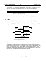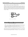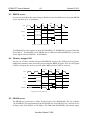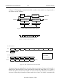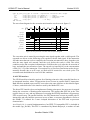
1
2015.1 The LEON2-FT Processor User’s Manual Version 2015.1 Feb. 25, 2015 Aeroflex Gaisler AB ESA / ESTEC 2 Copyright 2006 - 2015 Aeroflex Gaisler AB / European Space Agency The LEON-2 User’s Manual LEON2-FT User’s Manual 3 Version 2015.1 1 1.1 1.2 1.2.1 1.2.2 1.2.3 1.2.4 1.2.5 1.2.6 1.2.7 1.2.8 1.2.9 1.2.10 1.2.11 1.2.12 1.2.13 1.3 Introduction .................................................................................................... Overview ........................................................................................................ Functional overview ....................................................................................... Integer unit ..................................................................................................... Floating-point unit.......................................................................................... Cache sub-system ........................................................................................... Memory Management Unit ............................................................................ Debug support unit ......................................................................................... Memory interface ........................................................................................... Timers............................................................................................................. Watchdog........................................................................................................ UARTs............................................................................................................ Interrupt controller ......................................................................................... Parallel I/O port .............................................................................................. AMBA on-chip buses..................................................................................... Watchpoint registers....................................................................................... Performance.................................................................................................... 9 9 10 10 10 10 11 11 11 11 11 11 12 12 12 12 12 2 2.1 2.2 2.3 2.3.1 2.3.2 2.3.3 2.3.4 2.3.5 2.4 2.4.1 2.4.2 2.4.3 2.5 Simulation and synthesis ................................................................................ Un-packing the tar-file ................................................................................... Configuration.................................................................................................. Simulation ...................................................................................................... Compilation of the model............................................................................... Generic test bench .......................................................................................... Disassembler .................................................................................................. Simulator specific support.............................................................................. Post-synthesis simulation ............................................................................... Synthesis......................................................................................................... General ........................................................................................................... Synplify .......................................................................................................... Synopsys-DC.................................................................................................. GRFPU integration......................................................................................... 13 13 13 13 13 13 14 15 15 15 15 16 16 16 3 3.1 3.2 3.3 3.4 3.5 3.6 3.7 3.8 3.9 3.10 LEON integer unit .......................................................................................... Overview ........................................................................................................ Instruction pipeline......................................................................................... Multiply instructions ...................................................................................... Multiply and accumulate instructions ............................................................ Divide instructions ......................................................................................... Register file SEU protection........................................................................... Processor reset operation................................................................................ Exceptions ...................................................................................................... Hardware breakpoints..................................................................................... Floating-point unit.......................................................................................... 17 17 18 18 19 19 19 20 21 22 22 4 4.1 4.2 4.2.1 Cache sub-system ........................................................................................... Overview ........................................................................................................ Instruction cache............................................................................................. Operation ........................................................................................................ 23 23 24 24 LEON2-FT User’s Manual 4 Version 2015.1 4.2.2 4.3 4.3.1 4.3.2 4.3.3 4.3.4 4.4 4.5 4.6 4.7 4.8 Instruction cache tag....................................................................................... Data cache ...................................................................................................... Operation ........................................................................................................ Write buffer .................................................................................................... Data cache snooping....................................................................................... Data cache tag ................................................................................................ Cache flushing................................................................................................ Diagnostic cache access ................................................................................. Cache line locking .......................................................................................... Cache parity protection .................................................................................. Cache Control Register .................................................................................. 25 25 25 26 26 26 27 27 27 28 28 5 5.1 5.2 5.3 5.4 Memory management unit.............................................................................. ASI mappings ................................................................................................. Caches ............................................................................................................ MMU registers ............................................................................................... Translation look-aside buffer (TLB) .............................................................. 31 31 31 31 32 6 6.1 6.2 6.3 6.4 AMBA on-chip buses..................................................................................... Overview ........................................................................................................ AHB bus ......................................................................................................... APB bus.......................................................................................................... AHB transfers generated by the processor ..................................................... 33 33 33 33 33 7 7.1 7.2 7.2.1 7.2.2 7.2.3 7.2.4 7.2.5 7.3 7.3.1 7.3.2 7.4 7.4.1 7.4.2 7.5 7.5.1 7.5.2 7.5.3 7.5.4 7.5.5 7.5.6 7.6 7.6.1 7.7 7.8 On-chip peripherals ........................................................................................ On-chip registers ............................................................................................ Interrupt controller ......................................................................................... Operation ........................................................................................................ Interrupt (re)map registers.............................................................................. Reset values.................................................................................................... Interrupt assignment ....................................................................................... Control registers ............................................................................................. Secondary interrupt controller........................................................................ Operation ........................................................................................................ Control registers ............................................................................................. Timer unit ....................................................................................................... Operation ........................................................................................................ Registers ......................................................................................................... UARTs............................................................................................................ Transmitter operation ..................................................................................... Receiver operation.......................................................................................... Baud-rate generation ...................................................................................... Loop back mode ............................................................................................. Interrupt generation ........................................................................................ UART registers............................................................................................... Parallel I/O port .............................................................................................. PWM functionality ......................................................................................... LEON configuration register.......................................................................... Power-down.................................................................................................... 35 35 36 36 36 37 37 37 41 41 42 43 43 44 45 45 46 46 46 47 47 48 50 50 51 LEON2-FT User’s Manual 5 Version 2015.1 7.9 AHB status register ........................................................................................ 51 8 8.1 8.2 8.3 8.4 8.5 8.6 8.7 8.8 8.9 8.9.1 8.9.2 8.9.3 8.9.4 8.9.5 8.9.6 8.9.7 8.9.8 8.9.9 8.10 8.11 8.12 8.13 8.14 8.14.1 8.14.2 8.14.3 8.14.4 8.15 8.16 8.17 External memory access................................................................................. Memory interface ........................................................................................... Memory controller.......................................................................................... PROM access ................................................................................................. Memory mapped I/O ...................................................................................... SRAM access ................................................................................................. Burst cycles .................................................................................................... 8-bit and 16-bit PROM and SRAM access .................................................... 8- and 16-bit I/O access.................................................................................. SDRAM access............................................................................................... General ........................................................................................................... Address mapping............................................................................................ Initialisation.................................................................................................... Configurable SDRAM timing parameters...................................................... Refresh............................................................................................................ SDRAM commands ....................................................................................... Read cycles..................................................................................................... Write cycles.................................................................................................... Address bus connection.................................................................................. Memory EDAC .............................................................................................. Memory configuration register 1 (MCFG1)................................................... Memory configuration register 2 (MCFG2)................................................... Memory configuration register 3 (MCFG3)................................................... Write protection.............................................................................................. Overview ........................................................................................................ Address/mask write protection....................................................................... Start/end address write protection .................................................................. Generation of write protection ....................................................................... Using BRDYN ............................................................................................... Access errors .................................................................................................. Attaching an external DRAM controller ........................................................ 52 52 52 53 53 53 54 55 56 56 56 56 57 57 57 57 57 58 58 58 59 60 61 61 61 61 62 63 63 64 64 9 9.1 9.2 9.2.1 9.2.2 9.2.3 9.2.4 9.2.5 9.2.6 9.2.7 9.3 9.3.1 9.3.2 9.3.3 9.3.4 Hardware debug support ................................................................................ Overview ........................................................................................................ Debug support unit ......................................................................................... Overview ........................................................................................................ Trace buffer .................................................................................................... AHB trace buffer filtering .............................................................................. DSU memory map.......................................................................................... DSU control register....................................................................................... DSU breakpoint registers ............................................................................... DSU trap register............................................................................................ DSU communication link............................................................................... Operation ........................................................................................................ DSU UART control register........................................................................... DSU UART status register ............................................................................. Baud rate generation....................................................................................... 65 65 65 65 66 68 68 70 70 71 71 71 73 73 73 LEON2-FT User’s Manual 6 Version 2015.1 9.4 9.4.1 9.4.2 9.4.3 9.4.4 9.5 9.6 9.7 Common operations ....................................................................................... Instruction breakpoints ................................................................................... Single stepping ............................................................................................... Alternative debug sources .............................................................................. Booting from DSU ......................................................................................... Design limitations........................................................................................... DSU monitor .................................................................................................. External DSU signals ..................................................................................... 74 74 74 74 74 74 75 75 10 10.1 10.2 10.3 Signals ............................................................................................................ Memory bus signals........................................................................................ System interface signals ................................................................................. Signal description ........................................................................................... 76 76 76 77 11 11.1 11.2 11.3 11.3.1 11.3.2 11.3.3 11.3.4 11.4 11.4.1 11.4.2 11.5 VHDL model architecture .............................................................................. Model hierarchy ............................................................................................. Model coding style ......................................................................................... AMBA buses .................................................................................................. AMBA AHB................................................................................................... AHB cache aspects......................................................................................... AHB protection signals .................................................................................. APB bus.......................................................................................................... Floating-point unit and co-processor.............................................................. Generic CP interface ...................................................................................... FPU interface.................................................................................................. Triple-modular redundancy registers (TMRR) .............................................. 80 80 81 82 82 83 83 83 83 83 84 85 12 12.1 12.2 12.3 12.4 12.5 12.6 12.7 12.8 12.9 12.9.1 12.9.2 12.9.3 Model Configuration ...................................................................................... Synthesis configuration .................................................................................. Integer unit configuration............................................................................... FPU configuration .......................................................................................... Cache configuration ....................................................................................... Memory controller configuration ................................................................... Debug configuration....................................................................................... Peripheral configuration ................................................................................. Fault-tolerance configuration ......................................................................... AMBA configuration ..................................................................................... AHB master configuration ............................................................................. AHB slave configuration................................................................................ APB configuration.......................................................................................... 86 86 87 88 88 89 89 90 91 92 92 92 93 13 13.1 13.2 13.2.1 13.2.2 13.2.3 13.2.4 13.2.5 Porting to a new technology or synthesis tool................................................ General ........................................................................................................... Target specific mega-cells.............................................................................. Integer unit register-file.................................................................................. Parallel FPU & co-processor register file....................................................... Cache ram memory cells ................................................................................ Dual-port rams................................................................................................ Pads ................................................................................................................ 94 94 94 94 95 95 96 96 LEON2-FT User’s Manual 13.2.6 7 Version 2015.1 Adding a new technology or synthesis tool.................................................... 96 LEON2-FT User’s Manual 1 9 Version 2015.1 Introduction 1.1 Overview The LEON2-FT VHDL model implements a 32-bit processor conforming to the IEEE-1754 (SPARC V8) architecture. It is designed for embedded applications with the following features on-chip: separate instruction and data caches, hardware multiplier and divider, memory management unit, interrupt controller, debug support unit with trace buffer, two 24bit timers, two UARTs, power-down function, watchdog, 16-bit I/O port, PWM, and a flexible memory controller. New modules can easily be added using the on-chip AMBA AHB/APB buses. The VHDL model is fully synthesisable with most synthesis tools and can be implemented on both FPGAs and ASICs. Simulation can be done with all VHDL-87 compliant simulators. The LEON2-FT design includes advanced fault-tolerance features to withstand arbitrary single-event upset (SEU) errors without loss of data. The fault-tolerance is provided at design (VHDL) level, and does not require an SEU-hard semiconductor process, nor a custom cell library or special back-end tools. Note: this manual describes the full functionality of the LEON2-FT model. Through the model’s configuration record (see “Model Configuration” on page 88), parts of the described functionality can be suppressed or modified to generate a smaller or faster implementation. Note: Due to historical reasons, this documentation and the LEON2-FT VHDL model makes use of the term cache set to describe a cache way. When reading the documentation and code, cache set can (should) always be replaced with cache way. Aeroflex Gaisler / ESA LEON2-FT User’s Manual 10 Version 2015.1 1.2 Functional overview A block diagram of LEON2-FT can be seen in figure 1. LEON2-FT processor SPARC V8 Integer unit Debug Support Unit I-Cache IEEE-754 FPU MEIKO/GRFPU (opt.) PCI (InSilicon) (opt.) D-Cache SRMMU (opt.) AHB interface AMBA AHB Debug Serial Link Timers Memory Controller AHB Controller IrqCtrl UARTS I/O port AHB/APB Bridge AMBA APB 8/16/32/39-bits memory bus PROM I/O SRAM SDRAM Figure 1: LEON2-FT block diagram (blue items are not provided with model 1.2.1 Integer unit The LEON integer unit implements the full SPARC V8 standard, including all multiply and divide instructions. The number of register windows is configurable within the limit of the SPARC standard (2 - 32), with a default setting of 8. 1.2.2 Floating-point unit The LEON2-FT model can be interfaced to the Meiko FPU core owned by Oracle, or the more performant GRFPU provided by Aeroflex Gaisler. No FPU core is provided with the LEON2-FT IP core. 1.2.3 Cache sub-system Separate, multi-set instruction and data caches are provided, each configurable with 1 - 4 sets, 1 - 64 kbyte/set, 16 - 32 bytes per line. Sub-blocking is implemented with one valid bit per 32-bit word. The instruction cache uses streaming during line-refill to minimise refill latency. The data cache uses write-through policy and implements a double-word write- Aeroflex Gaisler / ESA LEON2-FT User’s Manual 11 Version 2015.1 buffer. The data cache can also perform bus-snooping on the AHB bus when the MMU is not present/enabled. 1.2.4 Memory Management Unit The LEON processor includes the interface for an optional memory management unit (MMU), compatible with the SPARC V8 Reference MMU specification. The MMU uses virtual caches and translate addresses between the processor’s virtual address space and the AHB physical address space. The physical address space can be extended to 36 bits through an AHB side-band signal. The MMU translation look-aside buffer (TLB) can be configured in both size and organisation (shared/separate, 1 - 32 TLB entries, incremental or LRU replacement). Note that only the MMU interface but not the MMU itself is provided with the LEON2FT processor. 1.2.5 Debug support unit The (optional) debug support unit (DSU) allows non-intrusive debugging on target hardware. The DSU allows to insert breakpoints and watchpoints, and access to all on-chip registers from a remote debugger. A trace buffer is provided to trace the executed instruction flow and/ or AHB bus traffic. The DSU has no impact on performance and has low area complexity. Communication to an outside debugger (e.g. GDB) is done using a dedicated UART (RS232). The AHB trace buffer implements optional filtering for specific masters and AHB address areas to reduce the amount of AHB transactions stored. 1.2.6 Memory interface The flexible memory interface provides a direct interface to PROM, memory mapped I/O devices, static RAM (SRAM) and synchronous dynamic RAM (SDRAM). The memory areas can be programmed to either 8-, 16- or 32-bit data width. 8- and 32-bit ROM/RAM memories can optionally be protected using a 7-bit BCH code, providing single-error correction and double-error detection capabilities. 1.2.7 Timers Two 24-bit timers are provided on-chip. The timers can work in periodic or one-shot mode. Both timers are clocked by a common 10-bit prescaler. 1.2.8 Watchdog A 24-bit watchdog is provided on-chip. The watchdog is clocked by the timer prescaler. When the watchdog reaches zero, an output signal (WDOG) is asserted. This signal can be used to generate system reset. 1.2.9 UARTs Two 8-bit UARTs are provided on-chip. The baud-rate is individually programmable and data is sent in 8-bits frames with one stop bit. Optionally, one parity bit can be generated and checked. Aeroflex Gaisler / ESA LEON2-FT User’s Manual 12 Version 2015.1 1.2.10 Interrupt controller The interrupt controller manages a total of 15 interrupts, originating from internal and external sources. Each interrupt can be programmed to one of two priority levels. A chained, secondary controller for up to 32 additional interrupts is also available. As optional feature, the interrupt controller can be implemented with functionality to allows dynamic remapping between bus interrupt lines and processor interrupt lines. 1.2.11 Parallel I/O port A 32-bit parallel I/O port is provided. 16 bits are always available and can be individually programmed by software to be an input or an output. An additional 16 bits are only available when the memory bus is configured for 8- or 16-bit operation. Some of the bits have alternate usage, such as UART inputs/outputs and external interrupts inputs. The standard PIO pins can optionally be used as 8 complementary pulse-width modulation outputs with configurable (common) period and duty cycles. 1.2.12 AMBA on-chip buses The processor has a full implementation of AMBA AHB and APB on-chip buses. A flexible configuration scheme makes it simple to add new IP cores. Also, all provided peripheral units implement the AMBA AHB/APB interface making it easy to add more of them, or reuse them on other processors using AMBA. 1.2.13 Watchpoint registers To aid software debugging, up to four watchpoint registers can be configured. Each register can cause a trap on an arbitrary instruction or data address range. If the debug support unit is enabled, the watchpoints can be used to enter debug mode. 1.3 Performance Using 4k + 4k caches and a 16x16 multiplier, the dhrystone 2.1 benchmark reports 1,550 iteration/s/MHz using the gcc-2.95.2 compiler (-O2). This translates to 0.9 dhrystone MIPS/ MHz using the VAX 11/780 value a reference for one MIPS. Aeroflex Gaisler / ESA LEON2-FT User’s Manual 2 13 Version 2015.1 Simulation and synthesis 2.1 Un-packing the tar-file The model is distributed as a gzipped tar-file; leon2ft-y.x.tar.gz. On unix systems, use the command ‘gunzip -c leon2ft-.y.x.tar.gz | tar xf -’ to unpack the model in the current directory. The LEON model has the following directory structure: leon leon/Makefile leon/boards leon/leon/ leon/modelsim/ leon/pmon leon/syn leon/tbench leon/tsource top directory top-level makefile fpga board support packages LEON vhdl model Modelsim simulator support files Boot-monitor Synthesis support files LEON VHDL test bench LEON test bench (C source) 2.2 Configuration The LEON model is highly configurable, allowing the model to be customised for a certain application or target technology. A graphical configuration tool based on the linux kernel tkconfig scripts is used to configure the model. In the leon top-level directory, do a ‘make xconfig’ on unix platforms or a ‘make wconfig’ on Windows/Cygwin platforms. After a configuration has been saved, the corresponding VHDL configuration file (device.vhd) will generated and installed when doing a ‘make dep’. Note that a working installation of GCC and Tcl/Tk must be installed on the host for tkconfig to work. A configuration can also be made by editing leon/device.vhd directly. The tkconfig tools has help texts for each configuration option - use those to derive a suitable configuration. For a more detailed description of the configuration options and their effects, see “Model Configuration” on page 88. The tkconfig tool allows loading of pre-defined configurations using the ‘Load configuration’ option and a few configuration files (config_xxx) are provided in the tkconfig directory. 2.3 Simulation 2.3.1 Compilation of the model On unix systems (or MS-windows with cygwin installed), the model and test benches can be built using ‘make’ in the top directory. Doing make without a target (or ‘make all’) will build the model and test benches using the modeltech compiler. Doing a ‘make vss’ will build the model with Synopsys VSS. To use another simulator, the makefiles in the leon and tbench sub-directories have to be modified to reflect the simulator commands. On non-unix systems, the compile.bat file in the leon and tbench directories can be used to compile the model in correct order. 2.3.2 Generic test bench A generic test bench is provided in tbench/tbgen.vhd. This test bench allows to generate a model of a LEON system with various memory sizes/types by setting the appropriate Aeroflex Gaisler / ESA LEON2-FT User’s Manual 14 Version 2015.1 generics. The file tbench/tbleon.vhd contains a number of alternative configurations using the generic test bench: • TB_FUNC8, TB_FUNC32, TB_FUNC_SD: Functional tests performing a quick check of most on-chip functions using either 8- or 32-bit external static ram, or 32-bit SDRAM. • TB_MEM: Testing all on-chip memory with patterns of 0x55 and 0xAA. • TB_FULL: Combined memory and functional tests, suitable to generate test vectors for manufacturing. Once the LEON model have been correctly configured and compiled, use the TB_FUNC32 test bench to verify the behaviour of the model. Simulation should be started in the top directory. Simulation can be started, for example, by typing vsim work.tb_func32 in a terminal and then, in the Modelsim shell, run -all command. The output from the simulation should be similar to: # # # # # # # # # # # *** Starting LEON system test *** # Memory interface test # Cache memory # Register file # Interrupt controller # Timers, watchdog and power-down # Parallel I/O port # UARTs # Test completed OK, halting with failure ** Failure: TEST COMPLETED OK, ending with FAILURE Simulation is halted by generating a failure. The supplied test program which is run by the test benches only tests on-chip peripherals and interfaces, compliance to the SPARC standard has been tested with proprietary test vectors, not supplied with the model. To re-compile the test program, the Bare-C GNU CrossCompiler System (BCC) provided by Aeroflex Gaisler (www.gaisler.com) needs to be installed; BCC versions 3.4.x and 4.4.x have been used for the current release, other versions might work but it is not guaranteed. The test programs are in the tsource directory and are built by executing ‘make’ in the tsource directory. The makefile will build the program and generate prom and ram images for the test bench. The test program probes the LEON configuration register to determine which options are enabled in the particular LEON configuration, and only tests those. E.g., if no FPU is present, the test program will not attempt to perform FPU testing. 2.3.3 Disassembler A SPARC disassembler is provided in the DEBUG package. It is used by the test bench to disassemble the executed instructions and print them to stdout (if enabled). Test bench configurations with names ending in a ‘_disas’ have disassembly enabled (e.g. TB_FUNC32_DISAS) Aeroflex Gaisler / ESA LEON2-FT User’s Manual 15 Version 2015.1 2.3.4 Simulator specific support The file modelsim/wave.do is a macro file for modelsim to display some useful internal LEON signals. A modelsim init file (modelsim.ini) is present in the top directory and in the leon and tbench directory to provide appropriate library mapping. The complete model can be compiled from within modelsim by executing the modelsim/compile.do file: vsim> do modelsim/compile.do A .synopsys_vss.setup file is present in the top directory and in the leon and tbench directory to provide appropriate library mapping for Synopsys VSS. 2.3.5 Post-synthesis simulation The supplied test-benches can be used to simulate the synthesised netlist. Use the following procedure: • Compile the complete model (i.e. do a ‘make’ at the top level). It is essential that you use the same configuration as during synthesis! This step is necessary because the test bench uses the target, config and device packages. • In the top directory, compile the simulation libraries for you ASIC/FPGA technology, and then your VHDL netlist. • Cd to tbench, and do ‘make clean all’. This will rebuild the test bench, ‘linking’ it with your netlist. • Cd back to the top directory and simulate you test bench as usual. • If you get problems with ‘X’ during simulation, use the TB_FULL test bench to make sure that all on-chip memories are properly initialised. 2.4 Synthesis 2.4.1 General The model is written with synthesis in mind and has been tested with Synopsys DC and Synplicity Synplify synthesis tools. Technology specific cells are used to implement the IU/ FPU register files, cache rams and pads. These cells can be automatically inferred (Synplify only) or directly instantiated from the target library (Synopsys). Non-synthesisable code is enclosed in a set of embedded pragmas as shown below: -- pragma translate_off ... non-synthesisable code... -- pragma translate_on This works with most synthesis tools, although hdlin_translate_off_skip_text variable be set to “true”. in Synopsys requires the Synthesis should be done from the ‘syn’ directory. It includes scripts/project-files for Synplify and Synopsys-DC. The source files are read from the leon directory, so it is essential that the model has been correctly configured before. Aeroflex Gaisler / ESA LEON2-FT User’s Manual 16 Version 2015.1 2.4.2 Synplify To synthesise LEON using Synplify, start synplify in the syn directory and open leon.prj. Make sure you use a version later than Synplify-8.2, some previous versions could generate a incorrect netlist under certain circumstances. 2.4.3 Synopsys-DC To synthesise LEON using Synopsys DC, start synopsys in the syn directory and execute the script leon.dcsh using dc_shell-xg-t -f leon.dcsh. Before executing the script, edit the beginning of the script to ensure that the library search paths reflects your synopsys installation and that the timing constraints are appropriate. The top-level constraints are used to generate the appropriate synopsys constraints commands. 2.5 GRFPU integration The GRFPU floating-point unit is not delivered with the standard LEON2-FT model, but can be obtained separately from Aeroflex Gaisler. The GRFPU is delivered as synthesized netlist, or encrypted RTL. Questions on the GRFPU should be directed to Aeroflex Gaisler via [email protected]. Aeroflex Gaisler / ESA LEON2-FT User’s Manual 3 17 Version 2015.1 LEON integer unit The LEON integer unit (IU) implements SPARC integer instructions as defined in SPARC Architecture Manual version 8. It is a new implementation, not based on any previous designs. The implementation is focused on portability and low complexity. 3.1 Overview The LEON integer unit has the following features: • • • • • • 5-stage instruction pipeline Separate instruction and data cache interface Support for 2 - 32 register windows Configurable multiplier (16x16, 32x1, 32x8, 32x16 & 32x32) Optional 16x16 bit MAC with 40-bit accumulator Radix-2 divider (non-restoring) Figure 2 shows a block diagram of the integer unit. call/branch address I-cache data address +1 Add ‘0’ jmpa tbr f_pc Fetch d_inst d_pc Decode imm, tbr, wim, psr e_inst e_pc rs1 operand2 Execute alu/shift mul/div y m_inst m_pc result Write w_pc wres Y 30 rd tbr, wim, psr regfile rs1 rs2 Figure 2: LEON integer unit block diagram Aeroflex Gaisler / ESA ex pc 30 jmpl address 32 32 address/dataout datain ytmp Memory w_inst 32 D-cache LEON2-FT User’s Manual 18 Version 2015.1 3.2 Instruction pipeline The LEON integer unit uses a single instruction issue pipeline with 5 stages: 1. FE (Instruction Fetch): If the instruction cache is enabled, the instruction is fetched from the instruction cache. Otherwise, the fetch is forwarded to the memory controller. The instruction is valid at the end of this stage and is latched inside the IU. 2. DE (Decode): The instruction is decoded and the operands are read. Operands may come from the register file or from internal data bypasses. CALL and Branch target addresses are generated in this stage. 3. EX (Execute): ALU, logical, and shift operations are performed. For memory operations (e.g., LD) and for JMPL/RETT, the address is generated. 4. ME (Memory): Data cache is accessed. For cache reads, the data will be valid by the end of this stage, at which point it is aligned as appropriate. Store data read out in the execution stage is written to the data cache at this time. 5. WR (Write): The result of any ALU, logical, shift, or cache read operations are written back to the register file. Table 1 lists the cycles per instruction (assuming cache hit and no load interlock): Instruction Cycles JMPL 2 Double load 2 Single store 2 Double store 3 SMUL/UMUL 1/2/4/5/35* SDIV/UDIV 35 Taken Trap 4 Atomic load/store 3 All other instructions 1 Table 1: Instruction timing * depends on multiplier configuration 3.3 Multiply instructions The LEON processor supports the SPARC integer multiply instructions UMUL, SMUL UMULCC and SMULCC. These instructions perform a 32x32-bit integer multiply, producing a 64-bit result. SMUL and SMULCC performs signed multiply while UMUL and UMULCC performs unsigned multiply. UMULCC and SMULCC also set the condition codes to reflect the result. Several multiplier implementation are provided, making it possible to choose between area, delay and latency (see “Integer unit configuration” on page 89 for more details). Aeroflex Gaisler / ESA LEON2-FT User’s Manual 19 Version 2015.1 3.4 Multiply and accumulate instructions To accelerate DSP algorithms, two multiply&accumulate instructions are implemented: UMAC and SMAC. The UMAC performs an unsigned 16-bit multiply, producing a 32-bit result, and adds the result to a 40-bit accumulator made up by the 8 lsb bits from the %y register and the %asr18 register. The least significant 32 bits are also written to the destination register. SMAC works similarly but performs signed multiply and accumulate. The MAC instructions execute in one clock but have two clocks latency, meaning that one pipeline stall cycle will be inserted if the following instruction uses the destination register of the MAC as a source operand. Assembler syntax: umac rs1, reg_imm, rd smac rs1, reg_imm, rd Operation: prod[31:0] = rs1[15:0] * reg_imm[15:0] result[39:0] = (Y[7:0] & %asr18[31:0]) + prod[31:0] (Y[7:0] & %asr18[31:0]) = result[39:0] rd = result[31:0] %asr18 can be read and written using the rdasr and wrasr instructions. 3.5 Divide instructions Full support for SPARC V8 divide instructions is provided (SDIV/UDIV/SDIVCC/ UDIVCC). The divide instructions perform a 64-by-32 bit divide and produce a 32-bit result. Rounding and overflow detection is performed as defined in the SPARC V8 standard. 3.6 Register file SEU protection To prevent erroneous operations from SEU errors in the main register file, each word can be protected using one parity bit, two parity bits or a 7-bit EDAC checksum. Checking of the parity or EDAC bits is done every time a fetched register value is used in an instruction. If a correctable error is detected, the erroneous data is corrected before being used. At the same time, the corrected register value is also written back to the register file. A correction operation incurs a delay 4 clock cycles, but has no other software visible impact. If an uncorrectable error is detected, a register error trap (tt=0x20) is generated. The implemented protection scheme has an impact on double-store instructions: the writebuffer will delay the request of the memory bus one clock cycle in order to not start any memory store cycle before the second store data word has been checked and (potentially) corrected. Aeroflex Gaisler / ESA LEON2-FT User’s Manual 20 Version 2015.1 The register file protection operation is controlled using application-specific register 16 (%asr16). The register is accessed using the RDASR/WRASR instructions. 31 12 11 10 9 RESERVED 8 CNT[2:0] 7 6 5 4 TCB[6:0] 3 2 1 0 TE DI Figure 1: Register file protection control register (%asr16) • • • • [0]: DI - disable checking. If set, will disable the register-file checking function. - 0 after reset [1]: TE - Test enable. - 0 after reset [8:2] TCB[6:0] - Test checkbits. [11:9] CNT[2:0] - Error counter. This field will be incremented for each corrected error. The protection can be disabled by setting the DI bit (this bit is set to ‘0’ after reset). By setting the TE bit, errors can be inserted in the register file to test the protection function. If a 7-bit EDAC is used and the test mode is enabled, the register checksum is XORed with the TCB field before written to the register file. If 2-bit parity is used, the parity bits and data bit 31 of dual-port ram 1 (corresponding to %rs1 operand) are XORed with TCB[2:0], while the parity bits and data bit 31 of dual-port ram 2 (corresponding to %rs2 operand) are XORed with TCB[5:3]. The CNT field is incremented each time a register correction is performed, but saturates at “111”. 3.7 Processor reset operation The processor is reset by asserting the RESET input for at least one clock cycle. The following table indicates the reset values of the registers which are affected by the reset. All other registers maintain their value (or are undefined). Register Reset value PC (program counter) 0x0 nPC (next program counter) 0x4 PSR (processor status register) ET=0, S=1 CCR (cache control register) 0x0 Table 2: Processor reset values Execution will start from address 0. Aeroflex Gaisler / ESA LEON2-FT User’s Manual 21 Version 2015.1 3.8 Exceptions LEON adheres to the general SPARC trap model. The table below shows the implemented traps and their individual priority. Trap TT Pri Description reset 0x00 1 Power-on reset write error 0x2b 2 write buffer error instruction_access_error 0x01 3 Error during instruction fetch illegal_instruction 0x02 5 UNIMP or other un-implemented instruction privileged_instruction 0x03 4 Execution of privileged instruction in user mode fp_disabled 0x04 6 FP instruction while FPU disabled cp_disabled 0x24 6 CP instruction while Co-processor disabled watchpoint_detected 0x0B 7 Hardware breakpoint match window_overflow 0x05 8 SAVE into invalid window window_underflow 0x06 8 RESTORE into invalid window register_hadrware_error 0x20 9 register file EDAC error (LEON-FT only) mem_address_not_aligned 0x07 10 Memory access to un-aligned address fp_exception 0x08 11 FPU exception cp_exception 0x28 11 Co-processor exception data_access_exception 0x09 13 Access error during load or store instruction tag_overflow 0x0A 14 Tagged arithmetic overflow divide_exception 0x2A 15 Divide by zero interrupt_level_1 0x11 31 Asynchronous interrupt 1 interrupt_level_2 0x12 30 Asynchronous interrupt 2 interrupt_level_3 0x13 29 Asynchronous interrupt 3 interrupt_level_4 0x14 28 Asynchronous interrupt 4 interrupt_level_5 0x15 27 Asynchronous interrupt 5 interrupt_level_6 0x16 26 Asynchronous interrupt 6 interrupt_level_7 0x17 25 Asynchronous interrupt 7 interrupt_level_8 0x18 24 Asynchronous interrupt 8 interrupt_level_9 0x19 23 Asynchronous interrupt 9 interrupt_level_10 0x1A 22 Asynchronous interrupt 10 interrupt_level_11 0x1B 21 Asynchronous interrupt 11 interrupt_level_12 0x1C 20 Asynchronous interrupt 12 interrupt_level_13 0x1D 19 Asynchronous interrupt 13 interrupt_level_14 0x1E 18 Asynchronous interrupt 14 interrupt_level_15 0x1F 17 Asynchronous interrupt 15 trap_instruction 0x80 0xFF 16 Software trap instruction (TA) Table 3: Trap allocation and priority Aeroflex Gaisler / ESA LEON2-FT User’s Manual 22 Version 2015.1 3.9 Hardware breakpoints The integer unit can be configured to include up to four hardware breakpoints. Each breakpoint consists of a pair of application-specific registers (%asr24/25, %asr26/27, %asr28/30 and %asr30/31) registers; one with the break address and one with a mask: %asr24, %asr26 %asr28, %asr30 %asr25, %asr27 %asr29, %asr31 31 2 1 WADDR[31:2] 31 2 WMASK[31:2] 0 IF 0 DL DS Figure 3: Watch-point registers Any binary aligned address range can be watched - the range is defined by the WADDR field, masked by the WMASK field (WMASK[x] = 1 enables comparison). On a breakpoint hit, trap 0x0B is generated. By setting the IF, DL and DS bits, a hit can be generated on instruction fetch, data load or data store. Clearing these three bits will effectively disable the breakpoint function. All the three bits are 0 after reset. 3.10 Floating-point unit The LEON model can be connected to the Meiko floating-point core or the GRFPU core, thereby providing full floating-point support according to the SPARC-V8 standard. The Meiko FPU is attached using an integrated interface inside the IU pipeline. The integrated FPU interface does not implement a floating-point queue, and the processor is stopped during the execution of floating-point instructions. This means that QNE bit in the %fsr register always is zero, and any attempts of executing the STDFQ instruction will generate a FPU exception trap. The GRFPU interface is controlled by a dedicated controller (GRFPC) which lets the FPU instructions execute in parallel with IU instructions and only halts the processor in case of data- or resource dependencies. The GRFPU and GRFPC IP cores can be licensed separately from Aeroflex Gaisler. When the LEON2-FT model is configured to use the GRFPU, the register file protection control register (%asr16) will control EDAC function of both integer and floating-point register files. When the test mode is enabled, integer instructions will insert errors in the integer register file while floating-point instructions will insert errors in the FP register file. Disabling EDAC protection will disable EDAC protection for both registers. The test checkbits field of the register file protection register is used to insert errors in both register files. The counter field is incremented for every register correction (in integer or floatingpoint registers). The FPU interface is enabled by setting the FPU element of the configuration record. Aeroflex Gaisler / ESA LEON2-FT User’s Manual 4 23 Version 2015.1 Cache sub-system 4.1 Overview The LEON processor implements a Harvard architecture with separate instruction and data buses, connected to two independent cache controllers. In addition to the address, a SPARC processor also generates an 8-bit address space identifier (ASI), providing up to 256 separate, 32-bit address spaces. During normal operation, the LEON processor accesses instructions and data using ASI 0x8 - 0xB as defined in the SPARC standard. Using the LDA/STA instructions, alternative address spaces can be accessed. The table shows the ASI usage for LEON. Only ASI[3:0] are used for the mapping, ASI[7:4] have no influence on operation. ASI Usage 0x0, 0x1, 0x2, 0x3 Forced cache miss (replace if cacheable) 0x4, 0x7 Forced cache miss (update on hit) 0x5 Flush instruction cache 0x6 Flush data cache 0x8, 0x9, 0xA, 0xB Normal cached access (replace if cacheable) 0xC Instruction cache tags 0xD Instruction cache data 0xE Data cache tags 0xF Data cache data 0x14 Data cache context id (mmu version only) 0x15 Instruction cache context id (mmu version only) 0x1c Bypass mmu translation (mmu version only) 0x19 MMU registers (mmu version only) Table 4: ASI usage Access to ASI 4 and 7 will force a cache miss, and update the cache if the data was previously cached. Access with ASI 0 - 3 will force a cache miss, update the cache if the data was previously cached, or allocated a new line if the data was not in the cache and the address refers to a cacheable location. The cacheable areas are by default the prom and ram areas, but are configurable in the model: Address range Area Cached 0x00000000 - 0x1FFFFFFF PROM Cacheable 0x20000000 - 0x3FFFFFFF I/O Non-cacheable 0x40000000 -0x7FFFFFFF RAM Cacheable 0x80000000 -0xFFFFFFFF Internal (AHB) Non-cacheable Table 5: Default cache table Both instruction and data cache controllers can be separately configured to implement a direct-mapped cache or a multi-set cache with set associativity of 2 - 4. The set size is Aeroflex Gaisler / ESA LEON2-FT User’s Manual 24 Version 2015.1 configurable to 1 - 64 kbyte divided into cache lines with 8 - 32 bytes of data. In the multiset configuration one of four replacement policies can be selected: least-recently-used (LRU), least-recently-replaced (LRR), (pseudo-) random allocation/replacement and (pseudo-) random replacement. If the LRR algorithm is used the cache has to be 2-way associative. A cache line can be locked in the instruction or data cache preventing it from being replaced by the replacement algorithm. NOTE: The LRR algorithm uses one extra bit in tag rams to store replacement history. The LRU algorithm needs extra flip-flops per cache line to store access history. The random replacement algorithm is implemented through modulo-N counter that selects which line to evict on cache miss. 4.2 Instruction cache 4.2.1 Operation The instruction cache can be configured as a direct-mapped cache or as a multi-set cache with associativity of 2 - 4 implementing either LRU or random replacement policies or as 2way associative cache implementing LRR algorithm. The set size is configurable to 1 - 64 kbyte and divided into cache lines of 16- 32 bytes. Each line has a cache tag associated with it consisting of a tag field, valid field with one valid bit for each 4-byte sub-block and optional LRR and lock bits. On an instruction cache miss to a cachable location, the instruction is fetched and the corresponding tag and data line updated. In a multi-set configuration a line to be replaced is chosen according to the replacement policy. If instruction burst fetch is enabled in the cache control register (CCR) the cache line is filled from main memory starting at the missed address and until the end of the line. At the same time, the instructions are forwarded to the IU (streaming). If the IU cannot accept the streamed instructions due to internal dependencies or multi-cycle instruction, the IU is halted until the line fill is completed. If the IU executes a control transfer instruction (branch/ CALL/JMPL/RETT/TRAP) during the line fill, the line fill will be terminated on the next fetch. If instruction burst fetch is enabled, incremental AHB bursts will be used on consecutive instruction fetches, even when the cache is disabled. In this case, the fetched instructions are only forwarded to the IU, the cache is not updated and a staggered burst will be observed. If a memory access error occurs during a line fill with the IU halted, the corresponding valid bit in the cache tag will not be set. If the IU later fetches an instruction from the failed address, a cache miss will occur, triggering a new access to the failed address. If the error remains, an instruction access error trap (tt=0x1) will be generated. Aeroflex Gaisler / ESA LEON2-FT User’s Manual 25 Version 2015.1 4.2.2 Instruction cache tag A instruction cache tag entry consists of several fields as shown in figure 4: Tag for 1 kbyte set, 32 bytes/line 31 10 9 8 7 0 LRR LOCK ATAG VALID Tag for 4 kbyte set, 16bytes/line 31 12 ATAG 9 00 8 LRR LOCK 3 0000 0 VALID Figure 4: Instruction cache tag layout examples Field Definitions: • [31:10]: Address Tag (ATAG) - Contains the tag address of the cache line. • [9]: LRR - Used by LRR algorithm to store replacement history. 0 if other replacement policy is used. • [8]: LOCK - Locks a cache line when set. 0 if instruction cache locking was not enabled in the configuration. • [7:0]: Valid (V) - When set, the corresponding sub-block of the cache line contains valid data. These bits is set when a sub-block is filled due to a successful cache miss; a cache fill which results in a memory error will leave the valid bit unset. A FLUSH instruction will clear all valid bits. V[0] corresponds to address 0 in the cache line, V[1] to address 1, V[2] to address 2 and so on. NOTE: only the necessary bits will be implemented in the cache tag, depending on the cache configuration. As an example, a 4 kbyte cache with 16 bytes per line would only have four valid bits and 20 tag bits. The cache rams are sized automatically by the ram generators in the model. 4.3 Data cache 4.3.1 Operation The data cache can be configured as a direct-mapped cache or as a multi-set cache with associativity of 2 - 4 implementing either LRU or (pseudo-) random replacement policy or as 2-way associative cache implementing LRR algorithm. The set size is configurable to 1 64 kbyte and divided into cache lines of 16 - 32 bytes. Each line has a cache tag associated with it consisting of a tag field, valid field with one valid bit for each 4-byte sub-block and optional lock and LRR bits. On a data cache read-miss to a cachable location 4 bytes of data are loaded into the cache from main memory. The write policy for stores is write-through with no-allocate on write-miss. In a multi-set configuration a line to be replaced on read-miss is chosen according to the replacement policy. If a memory access error occurs during a data load, the corresponding valid bit in the cache tag will not be set. and a data access error trap (tt=0x9) will be generated. Aeroflex Gaisler / ESA LEON2-FT User’s Manual 26 Version 2015.1 4.3.2 Write buffer The write buffer (WRB) consists of three 32-bit registers used to temporarily hold store data until it is sent to the destination device. For half-word or byte stores, the store data is replicated into proper byte alignment for writing to a word-addressed device, before being loaded into one of the WRB registers. The WRB is emptied prior to a load-miss cache-fill sequence to avoid any stale data from being read in to the data cache. Since the processor executes in parallel with the write buffer, a write error will not cause an exception to the store instruction. Depending on memory and cache activity, the write cycle may not occur until several clock cycles after the store instructions has completed. If a write error occurs, the currently executing instruction will take trap 0x2b. Note: the 0x2b trap handler should flush the data cache, since a write hit would update the cache while the memory would keep the old value due the write error. 4.3.3 Data cache snooping The data cache can optionally perform snooping on the AHB bus. When snooping is enabled, the data cache controller will monitor write accesses to the AHB bus performed by other AHB masters (DMA). When a write access is performed to a cacheable memory location, the corresponding cacheline will be invalidated in the data cache if present. Cache snooping has no overhead and does not affect performance. It can be dynamically enabled/disabled through bit 23 in the cache control register. Note that snooping is an optional feature and must be enabled in the VHDL configuration. Cache snooping requires the target technology to implement dual-port memories, which will be used to implement the cache tag RAM. It is not possible to enable snooping when an MMU is present in the system, since the cache addresses are virtual and the AHB addresses are physical. 4.3.4 Data cache tag A data cache tag entry consists of several fields as shown in figure 5: 31 10 9 8 LRR LOCK ATAG 7 0 VALID Figure 5: Data cache tag layout Field Definitions: • [31:10]: Address Tag (ATAG) - Contains the address of the data held in the cache line. • [9]: LRR - Used by LRR algorithm to store replacement history. ‘0’ if other replacement policy is used. • [8]: LOCK - Locks a cache line when set. ‘0’ if instruction cache locking was not enabled in the configuration. • [3:0]: Valid (V) - When set, the corresponding sub-block of the cache line contains valid data. These bits is set when a sub-block is filled due to a successful cache miss; a cache fill which results Aeroflex Gaisler / ESA LEON2-FT User’s Manual 27 Version 2015.1 in a memory error will leave the valid bit unset. V[0] corresponds to address 0 in the cache line, V[1] to address 1, V[2] to address 2 and V[3] to address 3. NOTE: only the necessary bits will be implemented in the cache tag, depending on the cache configuration. As an example, a 2 kbyte cache with 32 bytes per line would only have eight valid bits and 21 tag bits. The cache rams are sized automatically by the ram generators in the model. 4.4 Cache flushing The instruction and data cache is flushed by executing the FLUSH instruction, setting the FI bit in the cache control register, or by writing to any location with ASI=0x5. The flushing will take one cycle per cache line and set during which the IU will not be halted, but during which the instruction cache will be disabled. When the flush operation is completed, the cache will resume the state (disabled, enabled or frozen) indicated in the cache control register. 4.5 Diagnostic cache access Tags and data in the instruction and data cache can be accessed through ASI address space 0xC, 0xD, 0xE and 0xF by executing LDA and STA instructions. Address bits making up the cache offset will be used to index the tag to be accessed while the least significant bits of the bits making up the address tag will be used to index the cache set. Diagnostic read of tags is possible by executing an LDA instruction with ASI=0xC for instruction cache tags and ASI=0xE for data cache tags. A cache line and set are indexed by the address bits making up the cache offset and the least significant bits of the address bits making up the address tag. Similarly, the data sub-blocks may be read by executing an LDA instruction with ASI=0xD for instruction cache data and ASI=0xF for data cache data. The sub-block to be read in the indexed cache line and set is selected by A[4:2]. The tags can be directly written by executing a STA instruction with ASI=0xC for the instruction cache tags and ASI=0xE for the data cache tags. The cache line and set are indexed by the address bits making up the cache offset and the least significant bits of the address bits making up the address tag. D[31:10] is written into the ATAG field (see above) and the valid bits are written with the D[7:0] of the write data. Bit D[9] is written into the LRR bit (if enabled) and D[8] is written into the lock bit (if enabled). The data sub-blocks can be directly written by executing a STA instruction with ASI=0xD for the instruction cache data and ASI=0xF for the data cache data. The sub-block to be read in the indexed cache line and set is selected by A[4:2]. Note that diagnostic access to the cache is not possible during a FLUSH operation and will cause a data exception (trap=0x09) if attempted. 4.6 Cache line locking In a multi-set configuration the instruction and data cache controllers can be configured with optional lock bit in the cache tag. Setting the lock bit prevents the cache line to be replaced Aeroflex Gaisler / ESA LEON2-FT User’s Manual 28 Version 2015.1 by the replacement algorithm. A cache line is locked by performing a diagnostic write to the instruction tag on the cache offset of the line to be locked setting the Address Tag field to the address tag of the line to be locked, setting the lock bit and clearing the valid bits. The locked cache line will be updated on a read-miss and will remain in the cache until the line is unlocked. The first cache line on certain cache offset is locked in the set 0. If several lines on the same cache offset are to be locked the locking is performed on the same cache offset and in sets in ascending order starting with set 0. The last set can not be locked and is always replaceable. Unlocking is performed in descending set order. NOTE: Setting the lock bit in a cache tag and reading the same tag will show if the cache line locking was enabled during the LEON configuration: the lock bit will be set if the cache line locking was enabled otherwise it will be 0. 4.7 Cache parity protection Depending on the configuration of the VHDL model, the caches can be provided with one or two parity bits per tag and per 4-byte data sub-block. The tag parity is generated from the tag value, the valid bits and optionally the tag address. By including the tag address, it is also possible to detect errors in the cache ram address decoding logic. Similarly, the data subblock parity is derived from the sub-block address and the sub-block data. The parity bits are written simultaneously with the associated tag or sub-block and checked on each access. If two parity bits are configured, the bits correspond to the parity of odd and even data (tag) bits. If a tag parity error is detected during a cache access, a cache miss will be generated and the tag (and data) will be automatically updated. All valid bits except the one corresponding to the newly loaded data will be cleared. If a data sub-block parity error occurs, a miss will also be generated but only the failed sub-block will be updated with data from main memory. When the MMU is enabled, the tag parity generation will include the 8-bit context field. Parity errors will be handled in the same way as when the MMU is disabled. 4.8 Cache Control Register The operation of the instruction and data caches is controlled through a common Cache Control Register (CCR) (figure 5). Each cache can be in one of three modes: disabled, enabled and frozen. If disabled, no cache operation is performed and load and store requests are passed directly to the memory controller. If enabled, the cache operates as described above. In the frozen state, the cache is accessed and kept in sync with the main memory as if it was enabled, but no new lines are allocated on read misses. Aeroflex Gaisler / ESA LEON2-FT User’s Manual 31 29 Version 2015.1 30 29 28 27 26 25 24 23 22 21 20 19 18 17 16 15 14 13 12 11 10 9 DREPL IREPL ISETS DSETS DS FD FI CPC CPTE IB IP DP ITE IDE 8 DTE 7 6 5 4 3 DDE DF IF 2 DCS 1 0 ICS Figure 6: Cache control register • [31:30]: Data cache replacement policy (DREPL) - 01 - random, 10 - least-recently replaced (LRR), 11 - least-recently used (LRU). Read-only register. • [29:28]: Instruction cache replacement policy (IREPL) - 01 - random, 10 - least-recently replaced (LRR), 11 - least-recently used (LRU). Read-only register. • [27:26]: Instruction cache associativity (ISETS) - Number of sets in the instruction cache - 1: 00 - direct mapped, 01 - 2-way associative, 10 - 3-way associative, 11 - 4-way associative. Read-only register. • [25:24]: Data cache associativity (DSETS) - Number of sets in the data cache - 1: 00 - direct mapped, 01 - 2-way associative, 10 - 3-way associative, 11 - 4-way associative. Read-only register. • [23]: Data cache snoop enable [DS] - if set, will enable data cache snooping. Value 0 after reset. • [22]: Flush data cache (FD). If set, will flush the data cache. Always reads as zero. • [21]: Flush Instruction cache (FI). If set, will flush the instruction cache. Always reads as zero. • [20:19]: Cache parity bits (CPC) - Indicates how many parity bits are used to protect the caches (00=none, 01=1, 10=2). Read-only register. • [18:17]: Cache parity test bits. (CPTE). These bits are XOR’ed to the data and tag parity bits during diagnostic writes. • [16]: Instruction burst fetch (IB). This bit enables burst fill during instruction fetch. Value 0 after reset. • [15]: Instruction cache flush pending (IP). This bit is set when an instruction cache flush operation is in progress. Read-only register. • [14]: Data cache flush pending (DP). This bit is set when a data cache flush operation is in progress. Read-only register. • [13:12]: Instruction cache tag error counter (ITE) - This field is incremented every time an instruction cache tag parity error is detected. The counter saturates at 3 (‘11’) and shall be cleared in software so that new events can later be registered. • [11:10]: Instruction cache data error counter (IDE) - This field is incremented each time an instruction cache data sub-block parity error is detected. The counter saturates at 3 (‘11’) and shall be cleared in software so that new events can later be registered. • [9:8]: Data cache tag error counter (DTE) - This field is incremented every time a data cache tag parity error is detected. • [7:6]: Data cache data error counter (DDE) - This field is incremented each time an data cache data sub-block parity error is detected. • [5]: Data Cache Freeze on Interrupt (DF) - If set, the data cache will automatically be frozen when an asynchronous interrupt is taken. • [4]: Instruction Cache Freeze on Interrupt (IF) - If set, the instruction cache will automatically be frozen when an asynchronous interrupt is taken. Aeroflex Gaisler / ESA LEON2-FT User’s Manual 30 Version 2015.1 • [3:2]: Data Cache state (DCS) - Defines the current data cache state according to the following: X0= disabled, 01 = frozen, 11 = enabled. Set to ‘00’ at reset. • [1:0]: Instruction Cache state (ICS) - Defines the current instruction cache state according to the following: X0= disabled, 01 = frozen, 11 = enabled. Set to ‘00’ at reset. If the DF or IF bit is set, the corresponding cache will be frozen when an asynchronous interrupt is taken. This can be beneficial in real-time system to allow a more accurate calculation of worst-case execution time for a code segment. The execution of the interrupt handler will not evict any cache lines and when control is returned to the interrupted task, the cache state is identical to what it was before the interrupt. If a cache has been frozen by an interrupt, it can only be enabled again by enabling it in the CCR. This is typically done at the end of the interrupt handler before control is returned to the interrupted task. Aeroflex Gaisler / ESA LEON2-FT User’s Manual 5 31 Version 2015.1 Memory management unit A memory management unit (MMU) compatible with the SPARC V8 reference MMU can optionally be configured. For details on operation, see the SPARC V8 manual. 5.1 ASI mappings When the MMU is used, the following ASI mappings are made: ASI Usage 0x5 Flush instruction cache 0x6 Flush data cache 0x8, 0x9, 0xA, 0xB Normal cached access (replace if cacheable) 0xC Instruction cache tags 0xD Instruction cache data 0xE Data cache tags 0xF Data cache data 0x10 Flush page 0x13 Flush context 0x19 MMU registers 0x1C MMU bypass Table 6: MMU ASI usage 5.2 Caches When the MMU is disabled, the caches operate as normal with physical address mapping. When the MMU is enabled, the caches tags store the virtual address and also include an 8bit context field. AHB cache snooping is not available when the MMU is enabled. 5.3 MMU registers The following MMU registers are implemented: Address Register 0x000 MMU control register 0x100 Context pointer register 0x200 Context register 0x300 Fault status register 0x400 Fault address register Table 7: MMU registers (ASI = 0x19) The definition of the registers can be found in the SPARC V8 manual. Aeroflex Gaisler / ESA LEON2-FT User’s Manual 32 Version 2015.1 5.4 Translation look-aside buffer (TLB) The MMU can be configured to use a shared TLB, or separate TLB for instructions and data. The number of TLB entries can be set to 2 - 32 in the configuration record. The organisation of the TLB and number of entries is not visible to the software and does thus not require any modification to the operating system. Aeroflex Gaisler / ESA LEON2-FT User’s Manual 6 33 Version 2015.1 AMBA on-chip buses 6.1 Overview Two on-chip buses are provided: AMBA AHB and APB. The APB bus is used to access onchip registers in the peripheral functions, while the AHB bus is used for high-speed data transfers. The specification for the AMBA bus can be downloaded from ARM, at: www.arm.com. The AHB/APB bus controllers can be customised through the TARGET package. Additional (user defined) AHB/APB peripherals should be added in the MCORE module (see “Model hierarchy” on page 82). The AHB/APB busses follow the AMBA specification v. 2.0 with the following notes: - The AHB masters support AHB retry/split and error answers - The memory controller AHB slave never uses retry/split even on very long wait states - APB PREADY signal is not part of the AMBA v. 2.0 specification and therefore not supported. 6.2 AHB bus LEON uses the AMBA-2.0 AHB bus to connect the processor cache controllers to the memory controller and other (optional) high-speed units. In the default configuration, the processor is the only master on the bus, while two slaves are provided: the memory controller and the APB bridge. Table 8 below shows the default address allocation. Address range Size Mapping Module 0x00000000 - 0x1FFFFFFF 0x20000000 - 0x3FFFFFFF 0x40000000 - 0x7FFFFFFF 512 M 512 M 1G Prom Memory bus I/O SRAM and/or SDRAM Memory controller 0x80000000 - 0x8FFFFFFF 256 M On-chip registers APB bridge 0x90000000 - 0x9FFFFFFF 256 M Debug support unit DSU Table 8: Default AHB address allocation An attempt to access a non-existing device will generate an AHB error response. 6.3 APB bus The APB bridge is connected to the AHB bus as a slave and acts as the (only) master on the APB bus. Most on-chip peripherals are accessed through the APB bus. The address mapping of the APB bus can be seen in table 9. Optionally the implementation of a pipeline stage between the AHB slave port and APB master port can be selected, in case it is necessary to reduce the length of the critical path in this component. 6.4 AHB transfers generated by the processor The processor is connected to the AHB bus through the instruction and data cache controllers. Access conflicts between the two cache controllers are resolved locally and only Aeroflex Gaisler / ESA LEON2-FT User’s Manual 34 Version 2015.1 one AHB master interface is connected to the AHB bus. The processor will perform burst transfers to fetch instruction cache lines or reading/writing data as results of double load/ store instructions. Byte, half-word and word load/store instructions will perform single (nonsequential accesses. Locked transfers are only performed on LDST and SWAP instructions. Double load/store transfers are however also guaranteed to be atomic since the arbiter will not re-arbitrate the bus during burst transfers. Aeroflex Gaisler / ESA LEON2-FT User’s Manual 7 35 Version 2015.1 On-chip peripherals 7.1 On-chip registers A number of system support functions are provided directly on-chip. The functions are controlled through registers mapped APB bus according to the following table: Address Register Address 0x80000000 Memory configuration register 1 0x800000B0 Secondary interrupt mask register 0x80000004 Memory configuration register 2 0x800000B4 Secondary interrupt pending register 0x80000008 Memory configuration register 3 0x800000B8 Secondary interrupt status register 0x8000000C AHB Failing address register 0x800000B8 Secondary interrupt clear register 0x80000010 AHB status register 0x80000014 Cache control register 0x800000C4 DSU UART status register 0x80000018 Power-down register 0x800000C8 DSU UART control register 0x8000001C Write protection register 1 0x800000CC DSU UART scaler register 0x80000020 Write protection register 2 0x800000D0 Write protect start address 1 0x80000024 LEON configuration register 0x800000D4 Write protect start end 1 0x80000040 Timer 1 counter register 0x800000D8 Write protect start address 2 0x80000044 Timer 1 reload register 0x800000DC Write protect start end 2 0x80000048 Timer 1 control register 0x800000E0 Interrupt map register 0 0x8000004C Watchdog register 0x800000E4 Interrupt map register 1 0x80000050 Timer 2 counter register 0x80000054 Timer 2 reload register 0x80000058 Timer 2 control register 0x80000060 Prescaler counter register 0x80000064 Prescaler reload register 0x80000070 Uart 1 data register 0x80000074 Uart 1 status register 0x80000078 Uart 1 control register 0x8000007C Uart 1 scaler register 0x80000080 Uart 2 data register 0x80000084 Uart 2 status register 0x80000088 Uart 2 control register 0x8000008C Uart 2 scaler register 0x80000090 Interrupt mask and priority register 0x80000094 Interrupt pending register 0x80000098 Interrupt force register 0x8000009C Interrupt clear register 0x800000A0 I/O port input/output register 0x800000A4 I/O port direction register 0x800000A8 I/O port interrupt config. register 1 0x800000AC I/O port interrupt config. register 2 Table 9: On-chip registers Aeroflex Gaisler / ESA LEON2-FT User’s Manual 36 Version 2015.1 7.2 Interrupt controller The LEON interrupt controller is used to prioritize and propagate interrupt requests from internal or external devices to the integer unit. In total 15 interrupts are handled, divided on two priority levels. Figure 7 shows a block diagram of the interrupt controller. IRQ Pending DSU trace 32 2’nd IRQ controller Irq & trig select Priority encoder 15 4 IRL[3:0] 8 Timer 1 16 10 9 Timer 2 PIO[15:0] 11 4,5,6,7 10,12,13,15 IRQ Force IRQ mask Priority select 3 UART 1 2 UART 2 AHB error 1 Figure 7: Interrupt controller block diagram 7.2.1 Operation When an interrupt is generated, the corresponding bit is set in the interrupt pending register. The pending bits are ANDed with the interrupt mask register and then forwarded to the priority selector. Each interrupt can be assigned to one of two levels as programmed in the interrupt level register. Level 1 has higher priority than level 0. The interrupts are prioritised within each level, with interrupt 15 having the highest priority and interrupt 1 the lowest. The highest interrupt from level 1 will be forwarded to the IU - if no unmasked pending interrupt exists on level 1, then the highest unmasked interrupt from level 0 will be forwarded. When the IU acknowledges the interrupt, the corresponding pending bit will automatically be cleared. Interrupt can also be forced by setting a bit in the interrupt force register. In this case, the IU acknowledgement will clear the force bit rather than the pending bit. Note that interrupt 15 cannot be maskable by the integer unit and should be used with care most operating system do safely handle this interrupt. 7.2.2 Interrupt (re)map registers The interrupt controller can optionally be implemented (as an alternative to the two-interrupt levels scheme) with functionality to allow dynamic remapping between bus interrupt lines and processor interrupt lines. If the design includes this functionality then switch-logic will be placed on the incoming interrupt vector from the AMBA bus before the IRQ pending Aeroflex Gaisler / ESA LEON2-FT User’s Manual 37 Version 2015.1 register as shown in Figure 7. Two 32-bit Interrupt map registers will be available starting at offset 0x800000E0. The interrupt map registers contain one field for each bus interrupt line in the system. The value within this field determines to which LEON processor interrupt line the bus interrupt line is connected. In case several bus interrupt lines are mapped to the same processor interrupt line (several fields in the Interrupt map registers have the same value) then the bus interrupt lines will be OR:ed together. Note that if bus interrupt line X is remapped to processor interrupt line Y then bit Y of the pending register will be set when a peripheral asserts interrupt X. Remapping interrupt lines via the Interrupt map registers has the same effect as changing the interrupt assignments in the RTL code. 7.2.3 Reset values After reset, the interrupt mask register is set to all zeros while the remaining control registers are undefined. In case the Interrupt map registers are present then their reset value will correspond to a 1:1 mapping between bus interrupt and processor interrupts. 7.2.4 Interrupt assignment Table 10 shows the assignment of interrupt sources to the bus interrupt lines. Interrupt Source 15 Parallel I/O[7] 14 PCI (optional) 13 Parallel I/O[6] 12 Parallel I/O[5] 11 DSU trace buffer 10 Parallel I/O[4] 9 Timer 2 8 Timer 1 7 Parallel I/O[3] 6 Parallel I/O[2] 5 Parallel I/O[1] 4 Parallel I/O[0] 3 UART 1 2 UART 2 1 AHB error Table 10: Interrupt assignments 7.2.5 Control registers The operation of the interrupt controller is programmed through the following registers: Aeroflex Gaisler / ESA LEON2-FT User’s Manual 31 38 Version 2015.1 17 16 15 ILEVEL[15:1] R 1 IMASK[15:1] 0 R Figure 8: Interrupt mask and priority register Field Definitions: • [31:17]: Interrupt level (ILEVEL[15:1]) - indicates whether an interrupt belongs to priority level 1 (ILEVEL[n]=1) or level 0 (ILEVEL[n]=0). • [15:1]: Interrupt mask (IMASK[15:1]) - indicates whether an interrupt is masked (IMASK[n]=0) or enabled (IMASK[n]=1). All mask bits are 0 after reset. • [16], [0]: Reserved 31 16 15 1 IPEND[15:1] RESERVED 0 R Figure 9: Interrupt pending register Field Definitions: • [15:1]: Interrupt pending (IPEND[15:1]) - indicates whether an interrupt is pending (IPEND[n]=1). • [31:16], [0]: Reserved 31 16 15 1 IFORCE[15:1] RESERVED 0 R Figure 10: Interrupt force register Field Definitions: • [15:1]: Interrupt force (IFORCE[15:1]) - indicates whether an interrupt is being forced (IFORCE[n]=1). • [31:16], [0]: Reserved Aeroflex Gaisler / ESA LEON2-FT User’s Manual 39 31 Version 2015.1 16 15 1 ICLEAR[15:1] RESERVED 0 R Figure 11: Interrupt clear register Field Definitions: • [15:1]: Interrupt clear (ICLEAR[15:1]) - if written with a ‘1’, will clear the corresponding bit(s) in the interrupt pending register. A read returns zero. • [31:16], [0]: Reserved 31 28 27 24 23 20 19 16 15 12 11 8 7 4 3 0 RESERVED IRQMAP[1] ..IRQMAP[2] . ..IRQMAP[3].. .. .. . IRQMAP[4] .. IRQMAP[5] .. .. IRQMAP[6] .. IRQMAP[7] Figure 12: Interrupt map register 0 Field Definitions: • [31:28]: Reserved • [27:24]: Interrupt map for bus IRQ 1 - Bus interrupt 1 will be mapped to processor interrupt line IRQMAP[1]. • [23:20]: Interrupt map for bus IRQ 2- Bus interrupt 2 will be mapped to processor interrupt line IRQMAP[2]. • [19:16]: Interrupt map for bus IRQ 3 - Bus interrupt 3 will be mapped to processor interrupt line IRQMAP[3]. • [15:12]: Interrupt map for bus IRQ 4 - Bus interrupt 4 will be mapped to processor interrupt line IRQMAP[4]. • [11:8]: Interrupt map for bus IRQ 5 - Bus interrupt 5 will be mapped to processor interrupt line IRQMAP[5]. • [7:4]: Interrupt map for bus IRQ 6 - Bus interrupt 6 will be mapped to processor interrupt line IRQMAP[6]. • [3:0]: Interrupt map for bus IRQ 7 - Bus interrupt 7 will be mapped to processor interrupt line IRQMAP[7]. • Reset values are IRQMAP[i] = i meaning that, after reset, the interrupt map functionality has no visible effect Aeroflex Gaisler / ESA LEON2-FT User’s Manual 31 28 27 24 23 40 20 19 Version 2015.1 16 15 12 11 8 7 4 3 0 IRQMAP[8] . IRQMAP[9] .IRQMAP[10] . ..IRQMAP[11].. . IRQMAP[12] .. IRQMAP[13] .. IRQMAP[14] . IRQMAP[15] Figure 13: Interrupt map register 1 Field Definitions: • [31:28]: Reserved • [27:24]: Interrupt map for bus IRQ 8- Bus interrupt 8 will be mapped to processor interrupt line IRQMAP[8]. • [23:20]: Interrupt map for bus IRQ 9 - Bus interrupt 9 will be mapped to processor interrupt line IRQMAP[9]. • [19:16]: Interrupt map for bus IRQ 10- Bus interrupt 10 will be mapped to processor interrupt line IRQMAP[10]. • [15:12]: Interrupt map for bus IRQ 11- Bus interrupt 11 will be mapped to processor interrupt line IRQMAP[11]. • [11:8]: Interrupt map for bus IRQ 12 - Bus interrupt 12 will be mapped to processor interrupt line IRQMAP[12]. • [7:4]: Interrupt map for bus IRQ 13 - Bus interrupt 13 will be mapped to processor interrupt line IRQMAP[13]. • [3:0]: Interrupt map for bus IRQ 14 - Bus interrupt 14 will be mapped to processor interrupt line IRQMAP[14]. • [3:0]: Interrupt map for bus IRQ 15 - Bus interrupt 15 will be mapped to processor interrupt line IRQMAP[15]. • Reset values are IRQMAP[i] = i meaning that, after reset, the interrupt map functionality has no visible effect Aeroflex Gaisler / ESA LEON2-FT User’s Manual 41 Version 2015.1 7.3 Secondary interrupt controller The (optional) secondary interrupt controller is used add up to 32 additional interrupts, to be used by on-chip units in system-on-chip designs. Figure 7 shows a block diagram of the interrupt controller. IRQ Pending Priority encoder IRQ[31:0] 32 Filtering 32 5 IRL[4:0] IRQ10 IRQ mask Figure 14: Secondary interrupt controller block diagram 7.3.1 Operation The incoming interrupt signals are filtered according to the setting in the configuration record. The filtering condition can be one of four: active low, active high, negative edgetriggered and positive edge-triggered. When the condition is fulfilled, the corresponding bit is set in the interrupt pending register. The pending bits are ANDed with the interrupt mask register and then forwarded to the priority selector. If at least one unmasked pending interrupt exists, the interrupt output will be driven, generating interrupt 10 (by default). The highest unmasked pending interrupt can be read from the interrupt status register (see below). Interrupts are not cleared automatically upon a taken interrupt - the interrupt handler must reset the pending bit by writing a ‘1’ to the corresponding bit in the interrupt clear register. It must then also clear interrupt 10 in the primary interrupt controller. Testing of interrupts can be done by writing directly to the interrupt pending registers. Bits written with ‘1’ will be set while bits written with ‘0’ will keep their previous value. Note that not all 32 interrupts have to be implemented, how many are actually used depends on the configuration. Unused interrupts are ignored and the corresponding register bits are not generated. Mapping of interrupts to the secondary interrupt controller is done by editing mcore.vhd. See the configuration section on how to enable the controller and how to configure the interrupt filters. After reset, the interrupt mask register is set to all zeros while the remaining control registers are undefined. Aeroflex Gaisler / ESA LEON2-FT User’s Manual 42 Version 2015.1 7.3.2 Control registers The operation of the secondary interrupt controller is programmed through the following registers: 31 0 IMASK[31:0] Figure 15: Secondary interrupt mask register • [31:0]: Interrupt mask - indicates whether an interrupt is masked (IMASK[n]=0) or enabled (IMASK[n]=1). All bits are 0 after reset. 31 0 IPEND[31:0] Figure 16: Secondary interrupt pending register • [31:0]: Interrupt pending - indicates whether an interrupt is pending (IPEND[n]=1). All bits are 0 after reset. 31 5 IP RESERVED 4 0 IRL[4:0] Figure 17: Secondary interrupt status register • [4:0]: Interrupt request level - indicates the highest unmasked pending interrupt. • [5]: Interrupt pending - if set, then IRL is valid. If cleared, no unmasked interrupt is pending. 31 0 ICLEAR[31:0] Figure 18: Secondary interrupt clear register • [31:0]: Interrupt clear - if written with a ‘1’, will clear the corresponding bit(s) in the interrupt pending register. Aeroflex Gaisler / ESA LEON2-FT User’s Manual 43 Version 2015.1 7.4 Timer unit The timer unit implements two 32-bit timers, one 32-bit watchdog and one 10-bit shared prescaler (figure 19). timer1 reload prescaler reload timer2 reload prescaler value timer1 value irq 8 timer2 value irq 9 -1 tick watchdog WDOG -1 Figure 19: Timer unit block diagram 7.4.1 Operation The prescaler is clocked by the system clock and decremented on each clock cycle. When the prescaler underflows, it is reloaded from the prescaler reload register and a timer tick is generated for the two timers and watchdog. The effective division rate is therefore equal to prescaler reload register value + 1. The operation of the timers is controlled through the timer control register. A timer is enabled by setting the enable bit in the control register. The timer value is then decremented each time the prescaler generates a timer tick. When a timer underflows, it will automatically be reloaded with the value of the timer reload register if the reload bit is set, otherwise it will stop (at 0xffffffff) and reset the enable bit. An interrupt will be generated after each underflow. The timer can be reloaded with the value in the reload register at any time by writing a ‘one’ to the load bit in the control register. The watchdog operates similar to the timers, with the difference that it is always enabled and upon underflow asserts the external signal WDOG. This signal can be used to generate a system reset. To minimise complexity, the two timers and watchdog share the same decrementer. This means that the minimum allowed prescaler division factor is 4 (reload register = 3). Writes of values less than three to the prescaler reload or counter register will be ignored. Aeroflex Gaisler / ESA LEON2-FT User’s Manual 44 Version 2015.1 7.4.2 Registers Figures 20 to 24 shows the layout of the timer unit registers. 31 0 TIMER/WATCHDOG VALUE Figure 20: Timer 1/2 and Watchdog counter registers The watchdog counter register contains all 1s after reset (0xFFFFFFFF) 31 0 TIMER RELOAD VALUE Figure 21: Timer 1/2 reload registers 31 3 RESERVED 2 1 0 LD RL EN Figure 22: Timer 1/2 control registers • [2]: Load counter (LD) - when written with ‘one’, will load the timer reload register into the timer counter register. Always reads as a ‘zero’. • [1]: Reload counter (RL) - if RL is set, then the counter will automatically be reloaded with the reload value after each underflow. • [0]: Enable (EN) - enables the timer when set. Value 0 (timer disabled) after reset 31 10 9 RESERVED Figure 23: Prescaler reload register Aeroflex Gaisler / ESA 0 RELOAD VALUE LEON2-FT User’s Manual 45 Version 2015.1 Write of values <3 to the prescaler reload register will be ignored. After reset it is set to 3 when boot from RAM is selected, otherwise the reset value is (sysclk/1000000 -1). 31 10 9 RESERVED 0 COUNTER VALUE Figure 24: Prescaler counter register Write of values <3 to the prescaler counter register will be ignored. After reset it is set to 3 when boot from RAM is selected, otherwise the reset value is (sysclk/1000000 -1). 7.5 UARTs Two identical UARTs are provided for serial communications. The UARTs support data frames with 8 data bits, one optional parity bit and one stop bit. To generate the bit-rate, each UART has a programmable 12-bits clock divider. Hardware flow-control is supported through the RTSN/CTSN hand-shake signals. Figure 25 shows a block diagram of a UART. Baud-rate generator RXD Serial port Controller 8*bitclk Receiver shift register Transmitter shift register Receiver holding register Transmit. holding register CTSN RTSN TXD Internal I/O Bus Figure 25: UART block diagram 7.5.1 Transmitter operation The transmitter is enabled through the TE bit in the UART control register. When ready to transmit, data is transferred from the transmitter holding register to the transmitter shift register and converted to a serial stream on the transmitter serial output pin (TXD). It automatically sends a start bit followed by eight data bits, an optional parity bit, and one stop bits (figure 26). The least significant bit of the data is sent first Aeroflex Gaisler / ESA LEON2-FT User’s Manual 46 Version 2015.1 Data frame, no parity: Start D0 D1 D2 D3 D4 D5 D6 D7 Stop Data frame with parity: Start D0 D1 D2 D3 D4 D5 D6 D7 Parity Stop Figure 26: UART data frames Following the transmission of the stop bit, if a new character is not available in the transmitter holding register, the transmitter serial data output remains high and the transmitter shift register empty bit (TSRE) will be set in the UART control register. Transmission resumes and the TSRE is cleared when a new character is loaded in the transmitter holding register. If the transmitter is disabled, it will continue operating until the character currently being transmitted is completely sent out. The transmitter holding register cannot be loaded when the transmitter is disabled. If flow control is enabled, the CTSN input must be low in order for the character to be transmitted. If it is deasserted in the middle of a transmission, the character in the shift register is transmitted and the transmitter serial output then remains inactive until CTSN is asserted again. If the CTSN is connected to a receivers RTSN, overrun can effectively be prevented. 7.5.2 Receiver operation The receiver is enabled for data reception through the receiver enable (RE) bit in the USART control register. The receiver looks for a high to low transition of a start bit on the receiver serial data input pin. If a transition is detected, the state of the serial input is sampled a half bit clocks later. If the serial input is sampled high the start bit is invalid and the search for a valid start bit continues. If the serial input is still low, a valid start bit is assumed and the receiver continues to sample the serial input at one bit time intervals (at the theoretical centre of the bit) until the proper number of data bits and the parity bit have been assembled and one stop bit has been detected. The serial input is shifted through an 8-bit shift register where all bits have to have the same value before the new value is taken into account, effectively forming a low-pass filter with a cut-off frequency of 1/8 system clock. During reception, the least significant bit is received first. The data is then transferred to the receiver holding register (RHR) and the data ready (DR) bit is set in the USART status register. The parity, framing and overrun error bits are set at the received byte boundary, at the same time as the receiver ready bit is set. If both receiver holding and shift registers contain an un-read character when a new start bit is detected, then the character held in the receiver shift register will be lost and the overrun bit will be set in the UART status register. If flow control is enabled, then the RTSN will be negated (high) when a valid start bit is Aeroflex Gaisler / ESA LEON2-FT User’s Manual 47 Version 2015.1 detected and the receiver holding register contains an un-read character. When the holding register is read, the RTSN will automatically be reasserted again. 7.5.3 Baud-rate generation Each UART contains a 12-bit down-counting scaler to generate the desired baud-rate. The scaler is clocked by the system clock and generates a UART tick each time it underflows. The scaler is reloaded with the value of the UART scaler reload register after each underflow. The resulting UART tick frequency should be 8 times the desired baud-rate. If the EC bit is set, the scaler is bypassed and the UART will be clocked directly by the PIO[3] input rather than the system clock. In this case, the frequency of PIO[3] must be less than half the frequency of the system clock. 7.5.4 Loop back mode If the LB bit in the UART control register is set, the UART will be in loop back mode. In this mode, the transmitter output is internally connected to the receiver input and the RTSN is connected to the CTSN. It is then possible to perform loop back tests to verify operation of receiver, transmitter and associated software routines. In this mode, the outputs remain in the inactive state, in order to avoid sending out data. 7.5.5 Interrupt generation The UART will generate an interrupt under the following conditions: when the transmitter is enabled, the transmitter interrupt is enabled and the transmitter holding register moves from full to empty; when the receiver is enabled, the receiver interrupt is enabled and the receiver holding register moves from empty to full; when the receiver is enabled, the receiver interrupt is enabled and a character with either parity, framing or overrun error is received. 7.5.6 UART registers 31 8 7 0 RESERVED DATA Figure 27: UART data register • [7:0] : Receiver holding register (read access) • [7:0] : Transmitter holding register (write access) 8 31 RESERVED 7 6 5 4 2 1 0 EC LB FL PE PS TI RI TE RE Figure 28: UART control register • 0: Receiver enable (RE) - if set, enables the receiver. Value 0 after reset. • 1: Transmitter enable (TE) - if set, enables the transmitter. Value 0 after reset. • 2: Receiver interrupt enable (RI) - if set, enables generation of receiver interrupt. Aeroflex Gaisler / ESA 3 LEON2-FT User’s Manual • • • • • • 48 Version 2015.1 3: Transmitter interrupt enable (TI) - if set, enables generation of transmitter interrupt. 4: Parity select (PS) - selects parity polarity (0 = even parity, 1 = odd parity) 5: Parity enable (PE) - if set, enables parity generation and checking. 6: Flow control (FL) - if set, enables flow control using CTS/RTS. Value 0 after reset. 7: Loop back (LB) - if set, loop back mode will be enabled. 8: External Clock (EC) - if set, the scaler is bypassed and the UART will be clocked by PIO[3]. Value 0 after reset. 31 7 RESERVED 6 5 4 3 2 1 0 FE PE OV BR TH TS DR Figure 29: UART status register • 0: Data ready (DR) - indicates that new data is available in the receiver holding register. Value 0 after reset. • 1: Transmitter shift register empty (TS) - indicates that the transmitter shift register is empty. Value 1after reset. • 2: Transmitter hold register empty (TH) - indicates that the transmitter hold register is empty. Value 1after reset. • 3: Break received (BR) - indicates that a BREAK has been received; this bit is also writable to trigger a SW break. Value 0 after reset. • 4: Overrun (OV) - indicates that one or more character have been lost due to overrun. Value 0 after reset. • 5: Parity error (PE) - indicates that a parity error was detected. Value 0 after reset. • 6: Framing error (FE) - indicates that a framing error was detected. Value 0 after reset. 31 12 11 RESERVED 0 SCALER RELOAD VALUE Figure 30: UART scaler reload register When the “memory” boot option is selected, the reset value is not defined; otherwise the value can be equal to either the hard configuration record of the PIO[7..0] pins. Given the SCALER RELOAD VALUE, the baud rate can be computed as: baud-rate(bps) = Fclk / (8*Scaler_Reload_Value + 1) 7.6 Parallel I/O port A partially bit-wise programmable 32-bit I/O port is provided on-chip. The port is split in two parts - the lower 16-bits are accessible via the PIO[15:0] signal while the upper 16-bits uses D[15:0] and can only be used when all areas (rom, ram and I/O) of the memory bus are Aeroflex Gaisler / ESA LEON2-FT User’s Manual 49 Version 2015.1 in 8- or 16-bit mode (see “8-bit and 16-bit PROM and SRAM access” on page 56). If the SDRAM controller is enabled, the upper 16-bits cannot be used. The lower 16 bits of the I/O port can be individually programmed as output or input, while the high 16 bits of the I/O port only be configures as outputs or inputs on byte basis. Two registers are associated with the operation of the I/O port; the combined I/O input/output register, and I/O direction register. When read, the input/output register will return the current value of the I/O port; when written, the value will be driven on the port signals (if enabled as output). The direction register defines the direction for each individual port bit (0=input, 1=output). Direction D Q Output Value D Q Input Value Q D PAD Figure 31: I/O port block diagram 31 24 PWMEN[7:0] 23 18 17 PWMPERIOD 0 IODIR[17:0] Figure 32: I/O port direction register • IODIRn - I/O port direction. The value of IODIR[15:0] defines the direction of I/O ports 15 - 0. If bit n is set the corresponding I/O port becomes an output, otherwise it is an input. IODIR[16] controls D[15:8] while IODIR[17] controls D[7:0]. All bits are 0 after reset. • PWMPERIOD - PWM clock period (for more details look at section 7.6.1). Value 0 after reset. • PWMEN[7:0] - if PWMEN[n] is set, the PWM function on PIO(2*n) and PIO(2*n+1) is enabled. The I/O ports can also be used as interrupt inputs from external devices. A total of eight interrupts can be generated, corresponding to interrupt levels 4, 5, 6, 7, 10, 12, 13 and 15. The I/O port interrupt configuration registers 1 and 2 (figure 33) define which port should Aeroflex Gaisler / ESA LEON2-FT User’s Manual 50 Version 2015.1 generate each interrupt and how it should be filtered. 31 30 29 28 IOICFG1 EN LE PL 24 23 22 21 20 ISEL3 (IRQ7) 31 30 29 28 IOICFG2 EN LE PL EN LE PL 16 15 14 13 12 ISEL2 (IRQ6) 24 23 22 21 20 ISEL7 (IRQ15) EN LE PL EN LE PL 8 ISEL1 (IRQ5) 16 15 14 13 12 ISEL6 (IRQ13) EN LE PL 8 7 6 5 4 EN LE PL 7 6 5 ISEL5 (IRQ12) EN LE PL 0 ISEL0 (IRQ4) 4 0 ISEL4 (IRQ 10) Figure 33: I/O port interrupt configuration register 1 & 2 • ISELn - I/O port select. The value of this field defines which I/O port (0 - 31) should generate parallel I/O port interrupt n. • PLn - Polarity. If set, the corresponding interrupt will be active high (or edge-triggered on positive edge). Otherwise, it will be active low (or edge-triggered on negative edge). • LEn - Level/edge triggered. If set, the interrupt will be edge-triggered, otherwise level sensitive. • ENn - Enable. If set, the corresponding interrupt will be enabled, otherwise it will be masked. All interrupts are disabled after reset. If PWMENn is set, the concatenated 8 bits [ENn, LEn, PLn, ISELn] = PWMDCn are used to control the duty cycle of the PWM function on PIO(2*n) and PIO(2*n+1). To save pins, I/O pins are shared with other functions according to the table below: I/O port Function Type Description Enabling condition PIO[15] TXD1 Output UART1 transmitter data UART1 transmitter enabled PIO[14] RXD1 Input UART1 receiver data - PIO[13] RTS1 Output UART1 request-to-send UART1 flow-control enabled PIO[12] CTS1 Input UART1 clear-to-send - PIO[11] TXD2 Output UART2 transmitter data UART2 transmitter enabled PIO[10] RXD2 Input UART2 receiver data - PIO[9] RTS2 Output UART2 request-to-send UART2 flow-control enabled PIO[8] CTS2 Input UART2 clear-to-send - PIO[4] Boot select Input Internal or external boot prom - PIO[3] UART clock Input Use as alternative UART clock - PIO[1:0] Prom width Input Defines prom width at boot time - Table 11: UART/IO port usage 7.6.1 PWM functionality The 16 dedicated PIO pins can be used as eight PWM outputs. When the IO port has been implemented to support the PWM functionality the core will implement PWMs so that each PWM unit (i = 0..7) can be enabled separately with a configuration bit (bits 31:23 in the direction register) and provides complementary output on pins PIO(2*i) and PIO(2*i+1). The PWM clock is derived from a prescaler with hard configurable size (number of bits selectable via the tkconfig configuration tool). This clock is provided to an 8-bit periodic Aeroflex Gaisler / ESA LEON2-FT User’s Manual 51 Version 2015.1 counter whose period can be set to four times the PWMPERIOD field, located in the direction register. The duty cycle of each of the PWMs can be set with the interrupt configuration registers (PWMDCi associated with PWMi). Note that the corresponding interrupt cannot be generated when the corresponding PWM is enabled. 7.7 LEON configuration register Since LEON is synthesised from a extensively configurable VHDL model, the LEON configuration register (read-only) is used to indicate which options were enabled during synthesis. For each option present, the corresponding register bit is hardwired to ‘1’. Figure 34 shows the layout of the register. 31 30 29 28 27 26 25 24 20 19 NWINDOWS 17 16 15 14 ICSZ UMAC/SMAC inst Number of watchpoints SDRAM controller DSU present . ILSZ 12 11 10 9 DCSZ 8 7 6 5 4 3 2 1 0 DLSZ UDIV/SDIV inst. SMUL/UMUL inst. Watchdog present Memory status reg. FPU PCI core Write protection Figure 34: LEON configuration register • • • • • • • • • • • • • • • [30]: Debug support unit (0=disabled, 1=present) [29]: SDRAM controller present (0=disabled, 1=present) [28:26]: Number of implemented watchpoints (0 - 4) [25]: UMAC/SMAC instruction implemented [24:20]: Number of register windows. The implemented number of SPARC register windows -1. [19:17]: Instruction cache set size. The size (in kbytes) of each instruction cache set. Set size = 2ICSZ. [16:15]: Instruction cache line size.The line size (in 32-bit words) of each line. Line size = 2ILSZ. [14:12]: Data cache set size. The size (in kbytes) of each data cache set. Set size = 2DCSZ. [11:10]: Data cache line size. The line size (in 32-bit words) of each line. Line size = 2DLSZ. [9]: UDIV/SDIV instruction implemented [8]: UMUL/SMUL instruction implemented [6]: Memory status and failing address register present [5:4]: FPU type (00 = none, 01=Meiko) [3:2]: PCI core type (00=none, 01=InSilicon, 10=ESA, 11=other) [1:0]: Write protection type (00=none, 01=standard) 7.8 Power-down The processor can be powered-down by writing (an arbitrary) value to the power-down register. Power-down mode will be entered on the next load or store instruction. To enter power-down mode immediately, a store to the power-down register should be performed immediately followed by a ‘dummy’ load. During power-down mode, the integer unit will effectively be halted. The power-down mode will be terminated (and the integer unit reenabled) when an unmasked interrupt with higher level than the current processor interrupt Aeroflex Gaisler / ESA LEON2-FT User’s Manual 52 Version 2015.1 level (PIL) becomes pending. All other functions and peripherals operate as nominal during the power-down mode. A suitable power-down routine could be: struct pwd_reg_type { volatile int pwd; }; power_down() { struct pwd_reg_type *lreg = (struct pwd_reg_type *) 0x80000018; while (1) lreg->pwd = lreg->pwd; } In assembly, a suitable sequence could be: power_down: set 0x80000000, %l3 st %g0, [%l3 + 0x18] ba power_down ld [%l3 + 0x18], %g0 7.9 AHB status register Any access triggering an error response on the AHB bus will be registered in two registers; AHB failing address register and AHB status register. The failing address register will store the address of the access while the AHB status register will store the access and error types. The registers are updated when an error occur, and the EV (error valid) is set. When the EV bit is set, interrupt 1 is generated to inform the processor about the error. After an error, the EV bit has to be reset by software. Figure 35 shows the layout of the AHB status register. 31 9 RESERVED 8 7 EE EV RW 6 3 HMASTER 2 0 HSIZE Figure 35: AHB status register • • • • • [9]: EE - EDAC correctable error. Set when a correctable EDAC error is detected. [8]: EV - error valid. Set when an error occurred. Value 0 after reset. [7]: RW - Read/Write. This bit is set if the failed access was a read cycle, otherwise it is cleared. [6:3]: HMASTER - AHB master. This field contains the HMASTER[3:0] of the failed access. [2:0] HSIZE - transfer size. This field contains the HSIZE[2:0] of the failed transfer. Aeroflex Gaisler / ESA LEON2-FT User’s Manual 8 53 Version 2015.1 External memory access 8.1 Memory interface The memory bus provides a direct interface to PROM, memory mapped I/O devices, asynchronous static ram (SRAM) and synchronous dynamic ram (SDRAM). Chip-select decoding is done for two PROM banks, one I/O bank, five SRAM banks and two SDRAM banks. Figure 36 shows how the connection to the different device types is made. A ROMSN[1:0] OEN WRITEN CS OE WE PROM A IOSN CS OE WE I/O A CS OE WE SRAM A LEON RAMSN[4:0] RAMOEN[4:0] RWEN[3:0] SDCLK SDCSN[1:0] SDRASN SDCASN SDWEN SDDQM[3:0] CLK CSN RAS CAS WE DQM D D D D A[16:15] BA SDRAM A A[14:2] D A[27:0] D[31:0] Figure 36: Memory device interface 8.2 Memory controller The external memory bus is controlled by a programmable memory controller. The controller acts as a slave on the AHB bus. The function of the memory controller is programmed through memory configuration registers 1, 2 & 3 (MCR1, MCR2 & MCR3) through the APB bus. The memory bus supports four types of devices: prom, sram, sdram and local I/O. The memory bus can also be configured in 8- or 16-bit mode for applications with low memory and performance demands. The controller decodes a 2 Gbyte address space, divided according to table 12: Address range Size Mapping 0x00000000 - 0x1FFFFFFF 512 M Prom 0x20000000 - 0x3FFFFFFF 512M I/O 0x40000000 -0x7FFFFFFF 1G SRAM/SDRAM Table 12: Memory controller address map Aeroflex Gaisler / ESA LEON2-FT User’s Manual 54 Version 2015.1 8.3 PROM access Accesses to prom have the same timing as RAM accesses, the differences being that PROM cycles can have up to 15 waitstates. data1 data2 CLK A A1 ROMSN OEN D D1 Figure 37: Prom read cycle Two PROM chip-select signals are provided, ROMSN[1:0]. ROMSN[0] is asserted when the lower half (0 - 0x10000000) of the PROM area as addressed while ROMSN[1] is asserted for the upper half (0x10000000 - 0x20000000). 8.4 Memory mapped I/O Accesses to I/O have similar timing to ROM/RAM accesses, the differences being that a additional waitstates can be inserted by de-asserting the BRDYN signal. The I/O select signal (IOSN) is delayed one clock to provide stable address before IOSN is asserted. lead-in data lead-out CLK A A1 IOSN OEN D D1 BRDYN Figure 38: I/O read cycle 8.5 SRAM access The SRAM area can be up to 1 Gbyte, divided on up to five RAM banks. The size of banks 1-4 (RAMSN[3:0]is programmed in the RAM bank-size field (MCR2[12:9]) and can be set in binary steps from 8 kbyte to 256 Mbyte. The fifth bank (RAMSN[4]) decodes the upper Aeroflex Gaisler / ESA LEON2-FT User’s Manual 55 Version 2015.1 512 Mbyte. A read access to SRAM consists of two data cycles and between zero and three waitstates. Accesses to RAMSN[4] can further be stretched by de-asserting BRDYN until the data is available. On non-consecutive accesses, a turn-over cycle is added after a read cycle to prevent bus contention due to slow turn-off time of memories or I/O devices. During the turn-over cycle the address is not guaranteed to remain stable. Figure 39 shows the basic read cycle waveform (zero waitstate). data1 data2 turn-over CLK A A1 RAMSN RAMOEN D D1 Figure 39: Static ram read cycle (0-waitstate) For read accesses to RAMSN[4:0], a separate output enable signal (RAMOEN[n]) is provided for each RAM bank and only asserted when that bank is selected. A write access is similar to the read access but takes a minimum of three cycles: lead-in data lead-out CLK A A1 RAMSN RWEN D D1 Figure 40: Static ram write cycle Through an (optional) feed-back loop from the write strobes, the data bus is guaranteed to be driven until the write strobes are de-asserted. Each byte lane has an individual write strobe to allow efficient byte and half-word writes. If the memory uses a common write strobe for the full 16- or 32-bit data, the read-modify-write bit MCR2 should be set to enable readmodify-write cycles for sub-word writes. 8.6 Burst cycles To improve the bandwidth of the memory bus, accesses to consecutive addresses can be performed in burst mode. Burst transfers will be generated when the memory controller is Aeroflex Gaisler / ESA LEON2-FT User’s Manual 56 Version 2015.1 accessed using an AHB burst request. These includes instruction cache-line fills, double loads and double stores. The timing of a burst cycle is identical to the programmed basic cycle with the exception that during read cycles, the turn-over cycle will only occurs after the last transfer. 8.7 8-bit and 16-bit PROM and SRAM access To support applications with low memory and performance requirements efficiently, it is not necessary to always have full 32-bit memory banks. The SRAM and PROM areas can be individually configured for 8- or 16-bit operation by programming the ROM and RAM size fields in the memory configuration registers. Since read access to memory is always done on 32-bit word basis, read access to 8-bit memory will be transformed in a burst of four read cycles while access to 16-bit memory will generate a burst of two 16-bits reads. During writes, only the necessary bytes will be writen. Figure 41 shows an interface example with 8-bit PROM and 8-bit SRAM. Figure 42 shows an example of a 16-bit memory interface. 8-bit PROM CS OE WE ROMSN[0] OEN WRITEN LEON PROM A D A A[27:0] D[31:24] 8-bit RAM RAMSN[0] RAMOEN[0] RWEN[0] RWE[0] CS OE WE SRAM A D A[27:0] D[31:24] A[27:0] D[31:24] Figure 41: 8-bit memory interface example Aeroflex Gaisler / ESA D LEON2-FT User’s Manual 57 Version 2015.1 16-bit PROM ROMSN[0] OEN WRITEN CS OE WE LEON PROM A D A D A[27:1] D[31:16] 16-bit RAM RAMSN[0] RAMOEN[0] RWEN[0:1] CS OE RWE[1:0] WE SRAM A D A[27:1] D[31:16] A[27:0] D[31:16] Figure 42: 16-bit memory interface example 8.8 8- and 16-bit I/O access Similar to the PROM/RAM areas, the I/O area can also be configured to 8- or 16-bits mode. However, the I/O device will NOT be accessed by multiple 8/16 bits accesses as the memory areas, but only with one single access just as in 32-bit mode. To accesses an I/O device on a 16-bit bus, LDUH/STH instructions should be used while LDUB/STB should be used with an 8-bit bus. 8.9 SDRAM access 8.9.1 General Synchronous dynamic RAM (SDRAM) access is supported to two banks of PC100/PC133 compatible devices. The controller supports 64M, 256M and 512M device with 8 - 12 column-address bits, up to 13 row-address bits, and 4 banks. The size of each of the two banks can be programmed in binary steps between 4 Mbyte and 512 Mbyte. The operation of the SDRAM controller is controlled through MCFG2 and MCFG3 (see below). Note that only 32-bit data bus width is supported for SDRAM banks. 8.9.2 Address mapping The two SDRAM banks can be mapped starting at address 0x40000000 or 0x60000000. When the SDRAM enable bit is set in MCFG2, the controller is enabled and mapped at 0x60000000 as long as the SRAM disable bit is not set. If the SRAM disable bit is set, all access to SRAM is disabled and the SDRAM banks are mapped starting at 0x40000000. Aeroflex Gaisler / ESA LEON2-FT User’s Manual 58 Version 2015.1 8.9.3 Initialisation After reset, the controller automatically performs the SDRAM initialisation sequence of PRECHARGE, 2x AUTO-REFRESH and LOAD-MODE-REG on both banks simultaneously. The controller programs the SDRAM to use page burst on read and single location access on write. A CAS latency of 3 is programmed by default, but can be changed later by software issuing additional LOAD-MODE-REG commands. 8.9.4 Configurable SDRAM timing parameters To provide optimum access cycles for different SDRAM devices (and at different frequencies), some SDRAM parameters can be programmed through memory configuration register 2 (MCFG2) The programmable SDRAM parameters can be seen in table 13: Function Parameter range unit tCAS, tRCD 2-3 clocks Precharge to activate tRP 2-3 clocks Auto-refresh command period tRFC 3 - 11 clocks 10 - 32768 clocks CAS latency, RAS/CAS delay Auto-refresh interval Table 13: SDRAM programmable timing parameters Remaining SDRAM timing parameters are according the PC100/PC133 specification. 8.9.5 Refresh The SDRAM controller contains a refresh function that periodically issues an AUTOREFRESH command to both SDRAM banks. The period between the commands (in clock periods) is programmed in the refresh counter reload field in the MCFG3 register. Depending on SDRAM type, the required period is typically 7.8 or 15.6 s (corresponding to 780 or 1560 clocks at 100 MHz). The generated refresh period is calculated as (reload value+1)/ sysclk. The refresh function is enabled by setting bit 31 in MCFG2. 8.9.6 SDRAM commands The controller can issue three SDRAM commands by writing to the SDRAM command field in MCFG2: PRE-CHARGE, AUTO-REFRESH and LOAD-MODE-REG (LMR). If the LMR command is issued, the CAS delay as programmed in MCFG2 will be used, remaining fields are fixed: page read burst, single location write, sequential burst. The command field will be cleared after a command has been executed. Note that when changing the value of the CAS delay, a LOAD-MODE-REGISTER command should be generated at the same time. 8.9.7 Read cycles A read cycle is started by performing an ACTIVATE command to the desired bank and row, followed by a READ command after the programmed CAS delay. A read burst is performed if a burst access has been requested on the AHB bus. The read cycle is terminated with a PRE-CHARGE command, no banks are left open between two accesses. Aeroflex Gaisler / ESA LEON2-FT User’s Manual 59 Version 2015.1 8.9.8 Write cycles Write cycles are performed similarly to read cycles, with the difference that WRITE commands are issued after activation. A write burst on the AHB bus will generate a burst of write commands without idle cycles in-between. 8.9.9 Address bus connection The address bus of the SDRAMs should be connected to A[14:2], the bank address to A[16:15]. Devices with less than 13 address pins should leave the MSB part of A[14:2] unconnected. 8.10 Memory EDAC The memory controller in LEON2-FT is provided with an EDAC that can correct one error and detect two errors in a 32-bit word. For each word, a 7-bit checksum is generated according to the equations below. Correction is done on-the-fly and no timing penalty occurs during correction. If an un-correctable error (double-error) is detected, an memory exception is signalled to the IU. If a correctable error occurs, no exception is generated but the event is registered in the failing address and memory status register and interrupt 1 is generated. The interrupt can then be attached to a low priority interrupt handler that scrubs the failing memory location. The EDAC can be used during access to PROM or RAM areas by setting the corresponding EDAC enable bits in the Error control register (see below). The equations below show how the EDAC checkbits are generated: CB0 = D0 ^ D4 ^ D6 ^ D7 ^ D8 ^ D9 ^ D11 ^ D14 ^ D17 ^ D18 ^ D19 ^ D21 ^ D26 ^ D28 ^ D29 ^ D31 CB1 = D0 ^ D1 ^ D2 ^ D4 ^ D6 ^ D8 ^ D10 ^ D12 ^ D16 ^ D17 ^ D18 ^ D20 ^ D22 ^ D24 ^ D26 ^ D28 CB2 = D0 ^ D3 ^ D4 ^ D7 ^ D9 ^ D10 ^ D13 ^ D15 ^ D16 ^ D19 ^ D20 ^ D23 ^ D25 ^ D26 ^ D29 ^ D31 CB3 = D0 ^ D1 ^ D5 ^ D6 ^ D7 ^ D11 ^ D12 ^ D13 ^ D16 ^ D17 ^ D21 ^ D22 ^ D23 ^ D27 ^ D28 ^ D29 CB4 = D2 ^ D3 ^ D4 ^ D5 ^ D6 ^ D7 ^ D14 ^ D15 ^ D18 ^ D19 ^ D20 ^ D21 ^ D22 ^ D23 ^ D30 ^ D31 CB5 = D8 ^ D9 ^ D10 ^ D11 ^ D12 ^ D13 ^ D14 ^ D15 ^ D24 ^ D25 ^ D26 ^ D27 ^ D28 ^ D29 ^ D30 ^ D31 CB6 = D0 ^ D1 ^ D2 ^ D3 ^ D4 ^ D5 ^ D6 ^ D7 ^ D24 ^ D25 ^ D26 ^ D27 ^ D28 ^ D29 ^ D30 ^ D31 If the memory is configured in 8-bit mode, the EDAC checkbit bus (CB[7:0]) is not used but it is still possible to use EDAC protection. Data is always accessed as words (4 bytes at a time) and the corresponding checkbits are located at the address acquired by inverting the word address (address[27:2]) and using it as a byte address. The same chip-select is kept active. A word written as four bytes to addresses 0, 1, 2, 3 will have its checkbits at address 0x0FFFFFFF, addresses 4, 5, 6, 7 at 0x0FFFFFFE and so on. All the bits up to the maximum banksize will be inverted while the same chip-select is always asserted. This way all the banksize can be supported and no memory will be unused (except for a maximum of 4 B in the gap between the data and checkbit area). The 8-bit mode applies to RAM and PROM while SDRAM always uses 32-bit accesses. Only byte-writes should be performed to ROM with EDAC enabled. In this case, only the corresponding byte will be written. The operation of the EDAC can be tested trough the Error control register (see below). If the WB (write bypass) bit is set, the value in the TCB field will replace the normal checkbits during memory write cycles. If the RB (read bypass) is set, the memory checkbits of the loaded data will be stored in the TCB field during memory read cycles. NOTE: when the EDAC is enabled, the RMW bit in memory configuration register 2 must be set. Aeroflex Gaisler / ESA LEON2-FT User’s Manual 60 Version 2015.1 8.11 Memory configuration register 1 (MCFG1) Memory configuration register 1 is used to program the timing of rom and local I/O accesses. 31 30 29 28 27 26 25 24 23 AR PR I/O width I/O ready enable BEXCN enable 20 19 18 12 11 10 9 8 7 4 3 0 Prom write ws Prom read ws I/O waitstates I/O enable Prom write enable Prom width Figure 43: Memory configuration register 1 • [3:0]: Prom read waitstates. Defines the number of waitstates during prom read cycles (“0000”=0, “0001”=2, “0010”=4, ... “1111”=30). • [7:4]: Prom write waitstates. Defines the number of waitstates during prom write cycles (“0000”=0, “0001”=2, “0010”=4, ,... “1111”=30). • [9:8]: Prom width. Defines the data width of the prom area (“00”=8, “01”=16, “10”=32). • [10]: Reserved • [11]: Prom write enable. If set, enables write cycles to the prom area. • [18:12]: Unsused. • [19]: I/O enable. If set, the access to the memory bus I/O area are enabled. • [23:20]: I/O waitstates. Defines the number of waitstates during I/O accesses (“0000”=0, “0001”=1, “0010”=2,..., “1111”=15). • [25]: Bus error (BEXCN) enable. • [26]:Bus ready (BRDYN) enable. • [28:27]: I/O bus width. Defines the data width of the I/O area (“00”=8, “01”=16, “10”=32). • [29]: Asynchronous bus ready (ABRDYN). If set, the BRDYN input can be asserted without relation to the system clock. Reset to ‘0’ at power-up. • [30]: PROM area bus ready enable (PBRDYN). If set, a PROM access will be extended until BRDYN is asserted. Reset to ‘0’ at power-up. During power-up, the prom width (bits [9:8]) are set with value on PIO[1:0] inputs. The prom waitstates field is set to 15 (maximum) and the external bus error and bus ready are disabled. All other fields are undefined. Aeroflex Gaisler / ESA LEON2-FT User’s Manual 61 Version 2015.1 8.12 Memory configuration register 2 (MCFG2) Memory configuration register 2 is used to control the timing of the SRAM and SDRAM. 31 30 29 27 26 25 23 22 21 20 19 14 13 12 9 8 7 6 5 4 3 2 1 0 SE SI SRAM bank sz SDRAM command SDRAM Col. size SDRAM Bank size CAS delay, tRCD tRFC tRP Refresh enable BRDYN enable Read-mod.-write Ram width Write waitstates Read waitstates Figure 44: Memory configuration register 2 • [1:0]: Ram read waitstates. Defines the number of waitstates during ram read cycles (“00”=0, “01”=1, “10”=2, “11”=3). • [3:2]: Ram write waitstates. Defines the number of waitstates during ram write cycles (“00”=0, “01”=1, “10”=2, “11”=3). • [5:4]: Ram width. Defines the data width of the ram area (“00”=8, “01”=16, “1X”= 32). • [6]: Read-modify-write. Enable read-modify-write cycles on sub-word writes to 16- and 32-bit areas with common write strobe (no byte write strobe). • [7]: Bus ready enable. If set, will enable BRDYN for RAMSN[4] • [12:9]: Ram bank size. Defines the size of each ram bank (“0000”=8 kbyte, “0001”=16 kbyte... “1111”=256 Mbyte). • [13]: SI - SRAM disable. If set together with bit 14 (SDRAM enable), the static ram access will be disabled. • [14]: SE - SDRAM enable. If set, the SDRAM controller will be enabled. • [20:19] SDRAM command. Writing a non-zero value will generate an SDRAM command: “01”=PRECHARGE, “10”=AUTO-REFRESH, “11”=LOAD-COMMAND-REGISTER. The field is reset after command has been executed. • [22:21]: SDRAM column size. “00”=256, “01”=512, “10”=1024, “11”=4096 when bit[25:23]= “111”, 2048 otherwise. • [25:23]: SDRAM banks size. Defines the banks size for SDRAM chip selects: “000”=4 Mbyte, “001”=8 Mbyte, “010”=16 Mbyte .... “111”=512 Mbyte. • [26]: SDRAM CAS delay. Selects 2 or 3 cycle CAS delay (0/1). When changed, a LOADCOMMAND-REGISTER command must be issued at the same time. Also sets RAS/CAS delay (tRCD). • [29:27]: SDRAM tRFC timing. tRFC will be equal to 3 + field-value system clocks. • [30]: SDRAM tRP timing. tRP will be equal to 2 or 3 system clocks (0/1). • [31]: SDRAM refresh. If set, the SDRAM refresh will be enabled. Aeroflex Gaisler / ESA LEON2-FT User’s Manual 62 Version 2015.1 8.13 Memory configuration register 3 (MCFG3) MCFG3 is contains the reload value for the SDRAM refresh counter and to control and monitor the memory EDAC. It also contains the configuration of the register file EDAC. 31 30 27 RFC ME 11 10 SDRAM refresh counter reload value 9 8 WB RB RE PE 7 0 TCB[7:0] Figure 45: Memory configuration register 3 • [31:30]: Regfile check bits (RFC) - Indicates how many checkbits are used for the register file (00=none, 01=1, 10=2, 11=7 (EDAC)) • [29:28]: Reserved • [27]: Memory EDAC (ME) - Indicates if a memory EDAC is present • [26:12]: SDRAM refresh counter reload value. • [11]: WB - EDAC diagnostic write bypass • [10]: RB - EDAC diagnostic read bypass • [9]: RAM EDAC enable (RE) - Enable EDAC checking of the RAM area • [8]: PROM EDAC enable (PE) - Enable EDAC checking of the PROM area. At reset, this bit is initialised with the value of PIO[2] • [7:0]: TCB - Test checkbits. This field replaces the normal checkbits during store cycles when WB is set. TCB is also loaded with the memory checkbits during load cycles when RB is set. The period between each AUTO-REFRESH command is calculated as follows: tREFRESH = ((reload value) + 1) / SYSCLK 8.14 Write protection 8.14.1 Overview Write protection is provided to protect the RAM area against accidental over-writing. It is implemented with two methods: the address/mask method as implemented in the original LEON2 model, and an extended version using start/end addressing. 8.14.2 Address/mask write protection The address/mask write protection is implemented with two block protect units capable of disabling or enabling write access to a binary aligned memory block in the range of 32 kbyte - 1 Gbyte. Each block protect unit is controlled through a control register (figure 46). The units operate as follows: on each write access to RAM, address bits (29:15) are xored with the tag field in the control register, and anded with the mask field. A write protection hit is generated if the result is equal to zero, and the corresponding unit is enabled in block protect mode (BP = 1) or if the results is not zero and the unit is enabled in segment mode (BP = 0). Aeroflex Gaisler / ESA LEON2-FT User’s Manual 63 31 30 29 EN BP Version 2015.1 15 14 TAG[14:0] 0 MASK[14:0] Figure 46: Write protection register 1 & 2 • • • • [14:0] Address mask (MASK) - this field contains the address mask [29:15] Address tag (TAG) - this field is compared against address(29:15) [30] Block protect (BP) - if set, selects block protect mode [31] Enable (EN) - if set, enables the write protect unit 8.14.3 Start/end address write protection The start/end address write protect scheme contains two identical units that compare the AHB write address against a start and an end address. If operated in block protect mode (BP = 1) and the AHB write address is equal or higher than the start address and lower or equal to the end address, a write protect hit is generated. If operated in segment mode (BP = 0), a write protect hit is generated when the write address is lower than the START address, or higher than the END address. 31 1 29 0 00 START1 [29:2] BP 0 00 END1 [29:2] US SU 00 START2 [29:2] BP 0 00 END2 [29:2] US SU Figure 47: Start/end address Write protection registers • • • • • START [29:2] Contains the first address in the protected block END [29:2] Contains the last address in the protected block BP - Block protect. If set, selects block protect mode US - User mode. If set, write protection is enabled for user-mode accesses SU - Supervisor mode. If set, write protection is enabled for supervisor-mode access. The start address is calculated as 0x40000000 + START*4. The end address is calculated as 0x40000000 + END*4. Aeroflex Gaisler / ESA LEON2-FT User’s Manual 64 Version 2015.1 8.14.4 Generation of write protection The results from the two write protection schemes is combined together according to the following scheme: • If all enabled units operate in block protect mode, then a write protect error will be generated if any of the enabled units signal a write protection hit. • If at least one of the enabled units operates in segment mode, then a write protect error will be generated only if all units operating in segment mode signal a write protection hit. A write protection error will result in that the AHB write cycle is ended with an AHB error response and the data is not written to the memory. The ROM area can be write protected by clearing the write enable bit MCR1. 8.15 Using BRDYN The BRDYN signal can be used to stretch access cycles to the PROM or I/O areas, and the RAM area decoded by RAMSN[4]. The accesses will always have at least the preprogrammed number of waitstates as defined in memory configuration registers 1 & 2, but will be further stretched until BRDYN is asserted. If bit 29 in memory configuration register 1 is not set, then BRDYN is sampled synchronously on the rising edge if the system clock and should be asserted in the cycle preceding the last one. If bit 29 is set, the BRDYN can be asserted asynchronously with the system clock. In this case, the read data must be kept stable until the de-assertion of OEN/ RAMOEN. The use of BRDYN can be enabled separately for the PROM, I/O and RAM areas. data1 data2 waitstate CLK A A1 RAMSN[4] OEN D D1 BRDYN BEXCN Figure 48: BRDYN and BEXCN timing (synchronous) Aeroflex Gaisler / ESA LEON2-FT User’s Manual 65 data1 Version 2015.1 data2 waitstate CLK A A1 RAMSN[4] OEN D D1 BRDYN BEXCN Figure 49: BRDYN and BEXCN timing (asynchronous) 8.16 Access errors An access error can be signalled by asserting the BEXCN signal, which is sampled together with the data. If the usage of BEXCN is enabled in memory configuration register 1, an error response will be generated on the internal AMBA bus. BEXCN can be enabled or disabled through memory configuration register 1, and is active for all areas (PROM, I/O an RAM). data1 data2 CLK A A1 RAMSN OEN D D1 BEXCN Figure 50: Read cycle with BEXCN 8.17 Attaching an external DRAM controller To attach an external DRAM controller, RAMSN[4] should be used since it allows the cycle time to vary through the use of BRDYN. In this way, delays can be inserted as required for opening of banks and refresh.‘ Aeroflex Gaisler / ESA LEON2-FT User’s Manual 66 Version 2015.1 8.18 Lead-out cycles Lead-out cycles are those cycles at the end of a transaction where all the control signals are deasserted, but the address is guaranteed to be maintained. Such Lead-out cycles are inserted after write transactions in all modes (PROM / IO / RAM) and after IO read. Even though they may be observed in other transactions as well, they are not guaranteed in PROM / RAM read transactions. Aeroflex Gaisler / ESA LEON2-FT User’s Manual 9 67 Version 2015.1 Hardware debug support 9.1 Overview The LEON processor includes hardware debug support to aid software debugging on target hardware. The support is provided through two modules: a debug support unit (DSU) and a debug communication link (DCL). The DSU can put the processor in debug mode, allowing read/write access to all processor registers and cache memories. The DSU also contains a trace buffer which stores executed instructions and/or data transfers on the AMBA AHB bus. The debug communications link implements a simple read/write protocol and uses standard asynchronous UART communications (RS232C). LEON processor Trace Buffer DSUEN DSUBRE DSUACT Debug I/F LEON SPARC V8 Integer unit Debug Support Unit I-Cache D-Cache AHB interface AMBA AHB DSUTX DSURX Debug Comm. Link Figure 51: Debug support unit and comm. link 9.2 Debug support unit 9.2.1 Overview The debug support unit is used to control the trace buffer and the processor debug mode. The DSU is attached to the AHB bus as slave, occupying a 2 Mbyte address space. Through this address space, any AHB master can access the processor registers and the contents of the trace buffer. The DSU control registers can be accessed at any time, while the processor registers and caches can only be accessed when the processor has entered debug mode; optionally, access to the DSU can be restricted to only when the processor is running in supervisor mode. The trace buffer can be accessed only when tracing is disabled/completed. In debug mode, the processor pipeline is held and the processor state can be accessed by the DSU. Entering the debug mode can occur on the following events (also depending on the values of the DSU Control Register): • • • • • • • executing a breakpoint instruction (ta 1) integer unit hardware breakpoint/watchpoint hit (trap 0xb) rising edge of the external break signal (DSUBRE) setting the break-now (BN) bit in the DSU control register a trap that would cause the processor to enter error mode occurrence of any, or a selection of traps as defined in the DSU control register after a single-step operation Aeroflex Gaisler / ESA LEON2-FT User’s Manual 68 Version 2015.1 • DSU breakpoint hit The debug mode can only be entered when the debug support unit is enabled through an external pin (DSUEN). When the debug mode is entered, the following actions are taken: • PC and nPC are saved in temporary registers (accessible by the debug unit) • an output signal (DSUACT) is asserted to indicate the debug state • the timer unit is (optionally) stopped to freeze the LEON timers and watchdog The instruction that caused the processor to enter debug mode is not executed, and the processor state is kept unmodified. Execution is resumed by clearing the BN bit in the DSU control register or by de-asserting DSUEN. The timer unit will be re-enabled and execution will continue from the saved PC and nPC. Debug mode can also be entered after the processor has entered error mode, for instance when an application has terminated and halted the processor. The error mode can be reset and the processor restarted at any address. 9.2.2 Trace buffer The trace buffer consists of a circular buffer that stores executed instructions and/or AHB data transfers. A 30-bit counter is also provided and stored in the trace as time tag. The trace buffer operation is controlled through the DSU control register and the Trace buffer control register (see below). When the processor enters debug mode, tracing can be suspended, depending on the value of bit 26 of the control register. The size of the trace buffer is by default 128 lines (= 2 kbyte), but can be configured to 64 - 1024 lines in the VHDL model configuration record. The trace buffer is 128 bits wide, the information stored is indicated in table 14 and table 15 below: Bits Name Definition 127 AHB breakpoint hit Set to ‘1’ if a DSU AHB breakpoint hit occurred. 126 - Unused 125:96 Time tag The value of the time tag counter 95:92 IRL Processor interrupt request input 91:88 PIL Processor interrupt level (psr.pil) 87:80 Trap type Processor trap type (psr.tt) 79 Hwrite AHB HWRITE 78:77 Htrans AHB HTRANS 76:74 Hsize AHB HSIZE 73:71 Hburst AHB HBURST 70:67 Hmaster AHB HMASTER 66 Hmastlock AHB HMASTLOCK 65:64 Hresp AHB HRESP 63:32 Load/Store data AHB HRDATA or HWDATA 31:0 Load/Store address AHB HADDR Table 14: Trace buffer data allocation, AHB tracing mode Aeroflex Gaisler / ESA LEON2-FT User’s Manual 69 Version 2015.1 Bits Name Definition 127 Instruction breakpoint hit Set to ‘1’ if a DSU instruction breakpoint hit occurred. 126 Multi-cycle instruction Set to ‘1’ on the second and third instance of a multi-cycle instruction (LDD, ST or FPOP) 125:96 Time tag The value of the time tag counter 95:64 Load/Store parameters Instruction result, Store address or Store data 63:34 Program counter Program counter (2 lsb bits removed since they are always zero) 33 Instruction trap Set to ‘1’ if traced instruction trapped 32 Processor error mode Set to ‘1’ if the traced instruction caused processor error mode 31:0 Opcode Instruction opcode Table 15: Trace buffer data allocation, Instruction tracing mode During instruction tracing, one instruction is stored per line in the trace buffer with the exception of multi-cycle instructions. Multi-cycle instructions are entered two or three times in the trace buffer. For store instructions, bits [63:32] correspond to the store address on the first entry and to the stored data on the second entry (and third in case of STD). Bit 126 is set on the second and third entry to indicate this. A double load (LDD) is entered twice in the trace buffer, with bits [63:32] containing the loaded data. Multiply and divide instructions are entered twice, but only the last entry contains the result. Bit 126 is set for the second entry. For FPU operation producing a double-precision result, the first entry puts the MSB 32 bits of the results in bit [63:32] while the second entry puts the LSB 32 bits in this field. When a trace is frozen, interrupt 11 is generated. The DSU time tag counter is incremented each clock as long as the processor is running. The counter is stopped when the processor enters debug mode, and restarted when execution is resumed. 31 29 0 00 DSU TIME TAG VALUE Figure 52: Time tag counter The trace buffer control register contains two counters that contain the next address of the trace buffer to be written. Since the buffer is circular, it actually points to the oldest entry in the buffer. The counters are automatically incremented after each stored trace entry. 31 29 28 SFILT MFILT 27 26 25 24 23 AF TA TI 12 11 AHB INDEX 0 INST . INDEX Figure 53: Trace buffer control register • • • • • [11:0] : Instruction trace index counter [23:12] : AHB trace index counter [24] : Trace instruction enable [25] : Trace AHB enable [26] : AHB trace buffer freeze. If set, the AHB trace buffer will be frozen when the processor enters debug mode Aeroflex Gaisler / ESA LEON2-FT User’s Manual • • 70 Version 2015.1 [28:27] Slave filtering (SFILT) - Trace only accesses to addresses with a certain prefix (bits 31:28). 0 = trace all accesses, 1 = trace only accesses with prefix 0x8, 2 = trace only addresses with prefix 0xA, 3 = trace only addresses with prefix 0xB. (See documentation in next section) [31:29] Master filtering (MFILT) - Trace only accesses from AHB masters with a particular master index. 0 = trace accesses from all masters, X = 1..6 trace only accesses from master X, 7 = trace only accesses from master 0. (See documentation in next section) When both instructions and AHB transfers are traced (‘mixed mode tracing’), the buffer is divided on two halves. Instructions are stored in the lower half and AHB transfers in the upper half of the buffer. The MSB bit of the AHB index counter is then automatically kept high, while the MSB of the instruction index counter is kept low. When the AF bit in the trace control register is set, AHB tracing is stopped when the processor is in debug mode. When AF is cleared, tracing continues until the AHB trace enable bits are cleared. Note that the VHDL model configuration allows to disable the mixed-mode capability. In this case, only the instruction trace index counter is provided, and is used also during AHB tracing. Setting both TA and TI bits in the trace buffer control register is then illegal. 9.2.3 AHB trace buffer filtering AHB trace buffer filtering reduces the amount of AHB transactions dumped into the trace buffer and helps debugging the access from specific masters or to specific address areas on the AHB bus. Filtering is controlled through the Trace buffer control register fields SFILT and MFILT. The filter decoding logic can be easily adapted by changing the lines after the comment “-- AHB trace filter comparison” in the leon/dsu.vhd VHDL code. Please note that master and slave filtering is subtractive. An access will be traced only if it passes both filters. With a setting on MFILT = 2 and SFILT = 1 for example, only accesses from AHB master #2 to addresses starting with 0x8.. will be traced. Programming a 0 in both fields disables the trace filtering, all AHB accesses are traced. Note that regardless of the trace filter settings, AHB tracing also needs to be enabled with the usual configuration bits (bit 0 of the DSU control register and bit 25 of the Trace buffer control register). 9.2.4 DSU memory map Accesses to the DSU register interface will be inhibited, and an AMBA ERROR response will be generated, when the DSUEN signal is LOW. DSU memory map can be seen in table 16 below. Address Register 0x90000000 DSU control register 0x90000004 Trace buffer control register 0x90000008 Time tag counter 0x90000010 AHB break address 1 0x90000014 AHB mask 1 0x90000018 AHB break address 2 Table 16: DSU address space Aeroflex Gaisler / ESA LEON2-FT User’s Manual 71 Address Version 2015.1 Register 0x9000001C AHB mask 2 0x90010000 - 0x90020000 Trace buffer ..0 Trace bits 127 - 96 ...4 Trace bits 95 - 64 ...8 Trace bits 63 - 32 ...C Trace bits 31 - 0 0x90020000 - 0x90040000 IU/FPU register file 0x90080000 - 0x90100000 IU special purpose registers 0x90080000 Y register 0x90080004 PSR register 0x90080008 WIM register 0x9008000C TBR register 0x90080010 PC register 0x90080014 NPC register 0x90080018 FSR register 0x9008001C DSU trap register 0x90080040 - 0x9008007C ASR16 - ASR31 (when implemented) 0x90100000 - 0x90140000 Instruction cache tags 0x90140000 - 0x90180000 Instruction cache data 0x90180000 - 0x901C0000 Data cache tags 0x901C0000 - 0x90200000 Data cache data 0x90300000 - 0x90340000 Instruction cache context field (MMU only) 0x90380000 - 0x903C0000 Data cache context field (MMU only) Table 16: DSU address space The addresses of the IU/FPU registers depends on how many register windows has been implemented and if and FPU is present. The registers can be accessed at the following addresses (NWINDOWS = number of SPARC register windows; 0 <= window < NWINDOWS, the window containing the register we want to examine): • • • • • • • %on %ln %in %gn %gn %fn %fn : 0x90020000 + (((window * 64) + 32 + 4*n) mod (NWINDOWS*64)) : 0x90020000 + (((window * 64) + 64 + 4*n) mod (NWINDOWS*64)) : 0x90020000 + (((window * 64) + 96 + 4*n) mod (NWINDOWS*64)) : 0x90020000 + (NWINDOWS*64) + 4*n (no FPU) : 0x90020000 + (NWINDOWS*64) + 128 + 4*n (FPU present) : 0x90020000 + (NWINDOWS*64) + 4*n (Meiko) : 0x90030000 + 4*n (GRFPU) When the MMU is present, the following MMU registers can be accessed by the DSU: Address Register 0x901E0000 MMU control register 0x901E0004 MMU context register 0x901E0008 MMU context table pointer register 0x901E000C MMU fault status register Table 17: MMU registers address space Aeroflex Gaisler / ESA LEON2-FT User’s Manual Address 72 Version 2015.1 Register 0x901E0010 MMU fault address register Table 17: MMU registers address space 9.2.5 DSU control register The DSU is controlled by the DSU control register: 31 20 19 18 17 16 15 14 13 12 11 10 9 DCNT 8 7 6 5 4 3 2 1 0 RE DR LR SS PE EE EB DM DE BZ BX BB BN BS BW BE FT BT DM TE Figure 54: DSU control register • • • • • • • • • • • • • • • • • • • • • 0: Trace enable (TE). Enables the trace buffer. Value 0 after reset. 1: Delay counter mode (DM). In mixed tracing mode, setting this bit will cause the delay counter to decrement on AHB traces. If reset, the delay counter will decrement on instruction traces. 2: Break on trace (BT) - if set, will generate a DSU break condition on trace freeze. Value 0 after reset. 3: Freeze timers (FT) - if set, the scaler in the LEON timer unit will be stopped during debug mode to preserve the time for the software application. Value 0 after reset. 4: Break on error (BE) - if set, will force the processor to debug mode when the processor would have entered error condition (trap in trap). 5: Break on IU watchpoint - if set, debug mode will be forced on a IU watchpoint (trap 0xb). 6: Break on S/W breakpoint (BS) - if set, debug mode will be forced when an breakpoint instruction (ta 1) is executed. Value 0 after reset. 7: Break now (BN) -Force processor into debug mode. If cleared, the processor will resume execution. 8: Break on DSU breakpoint (BD) - if set, will force the processor to debug mode when an DSU breakpoint is hit. Value 0 after reset. 9: Break on trap (BX) - if set, will force the processor into debug mode when any trap occurs. 10: Break on error traps (BZ) - if set, will force the processor into debug mode on all except the following traps: priviledged_instruction, fpu_disabled, window_overflow, window_underflow, asynchronous_interrupt, ticc_trap. 11: Delay counter enable (DE) - if set, the trace buffer delay counter will decrement for each stored trace. This bit is set automatically when an DSU breakpoint is hit and the delay counter is not equal to zero. Value 0 after reset. 12: Debug mode (DM). Indicates when the processor has entered debug mode (read-only). 13: EB - value of the external DSUBRE signal (read-only) 14: EE - value of the external DSUEN signal (read-only) 15: Processor error mode (PE) - returns ‘1’ on read when processor is in error mode, else ‘0’. Read-only bit. 16: Single step (SS) - if set, the processor will execute one instruction and the return to debug mode. Value 0 after reset. 17: Link response (LR) - is set, the DSU communication link will send a response word after AHB transfer. Value 0 after reset. 18: Debug mode response (DR) - if set, the DSU communication link will send a response word when the processor enters debug mode. Write only bit, it always reads 0. 19: Reset error mode (RE) - if set, will clear the error mode in the processor. 31:20 Trace buffer delay counter (DCNT). Note that the number of bits actually implemented depends on the size of the trace buffer. Bits 4, 5, 7, 9, 10 during reset are initialized with the value of the DSUBRE signal feed through a 3 stage synchronizer. 9.2.6 DSU breakpoint registers The DSU contains two breakpoint registers for matching either AHB addresses or executed processor instructions. A breakpoint hit is typically used to freeze the trace buffer, but can also put the processor in debug mode. Freezing can be delayed by programming the DCNT Aeroflex Gaisler / ESA LEON2-FT User’s Manual 73 Version 2015.1 field in the DSU control register to a non-zero value. In this case, the DCNT value will be decremented for each additional trace until it reaches zero, after which the trace buffer is frozen. If the BT bit in the DSU control register is set, the DSU will force the processor into debug mode when the trace buffer is frozen. Note that due to pipeline delays, up to 4 additional instruction can be executed before the processor is placed in debug mode. A mask register is associated with each breakpoint, allowing breaking on a block of addresses. Only address bits with the corresponding mask bit set to ‘1’ are compared during breakpoint detection. To break on executed instructions, the EX bit should be set. To break on AHB load or store accesses, the LD and/or ST bits should be set. Break address reg. Break mask reg. 31 2 1 0 0 EX BADDR[31:2] 31 2 1 0 LD ST BMASK[31:2] Figure 55: DSU breakpoint registers • • • • • BADDR : breakpoint address (bits 31:2) EX : break on instruction BMASK : Breakpoint mask (see text) LD : break on data load address ST : beak on data store address 9.2.7 DSU trap register The DSU trap register is a read-only register that indicates which SPARC trap type that caused the processor to enter debug mode. When debug mode is force by setting the BN bit in the DSU control register, the trap type will be 0xb (hardware watchpoint trap). 31 13 12 11 RESERVED EM 4 TRAP TYPE 3 0 0000 Figure 56: DSU trap register • • [11:4] : 8-bit SPARC trap type 12 : Error mode (EM). Set if the trap would have cause the processor to enter error mode. 9.3 DSU communication link 9.3.1 Operation The DSU communication link consists of a UART connected to the AHB bus as a master (figure 57). A simple communication protocol is supported to transmit access parameters and data. A link command consist of a control byte, followed by a 32-bit address, followed by optional write data. If the LR bit in the DSU control register is set, a response byte will be sent after each AHB transfer. If the LR bit is not set, a write access does not return any response, while a read access only returns the read data. Data is sent on 8-bit basis as shown Aeroflex Gaisler / ESA LEON2-FT User’s Manual 74 Version 2015.1 in figure 59. Through the communication link, a read or write transfer can be generated to any address on the AHB bus. Baud-rate generator DSURX Serial port Controller 8*bitclk AMBA APB Receiver shift register Transmitter shift register AHB master interface AHB data/response DSUTX AMBA AHB Figure 57: DSU communication link block diagram Start D0 D1 D2 D3 D4 D5 D6 D7 Stop Figure 58: DSU UART data frame DSU Write Command 11 Length -1 Send Receive Resp. byte Addr[31:24] Addr[23:16] Addr[15:8] Addr[7:0] Data[31:24] Data[23:16] Data[15:8] Data[7:0] (optional) Response byte encoding DSU Read command Send Receive 10 Length -1 Addr[31:24] Addr[23:16] Addr[15:8] Addr[7:0] Data[31:24] Data[23:16] Data[15:8] Data[7:0] Resp. byte bit 7:3 = 00000 bit 2 = DMODE bit 1:0 = AHB HRESP (optional) Figure 59: DSU Communication link commands A response byte can optionally be sent when the processor goes from execution mode to debug mode. Block transfers can be performed be setting the length field to n-1, where n denotes the number of transferred words. For write accesses, the control byte and address is sent once, followed by the number of data words to be written. The address is automatically Aeroflex Gaisler / ESA LEON2-FT User’s Manual 75 Version 2015.1 incremented after each data word. For read accesses, the control byte and address is sent once and the corresponding number of data words is returned. Note that any accesses by the DSU UART are always in supervisor mode (HPROT = “0011”). The UART receiver is implemented with same glitch filtering as the nominal UARTs. 9.3.2 DSU UART control register 31 2 RESERVED 1 0 BL EN Figure 60: UART control register • 0: Receiver enable (RE) - if set, enables both the transmitter and receiver. Value 0 after reset. • 1: Baud rate locked (BL) - is automatically set when the baud rate is locked. Value 0 after reset. 9.3.3 DSU UART status register 31 7 RESERVED 6 FE 5 4 3 2 1 0 OVBR TH TS DR Figure 61: UART status register • 0: Data ready (DR) - indicates that new data has been received and not yet read-out by the AHB master interface. Value 0 after reset. • 1: Transmitter shift register empty (TS) - indicates that the transmitter shift register is empty. Value 1 after reset. • 2: Transmitter hold register empty (TH) - indicates that the transmitter hold register is empty. Value 1after reset. • 3: Break (BR): SW break, starting a new baud-rate acquisition. • 4: Overrun (OV) - indicates that one or more character have been lost due to overrun. Value 0 after reset. • 6: Framing error (FE) - indicates that a framing error was detected. Value 0 after reset. 9.3.4 Baud rate generation The UART contains a 18-bit down-counting scaler to generate the desired baud-rate. The scaler is clocked by the system clock and generates a UART tick each time it underflows. The scaler is reloaded with the value of the UART scaler reload register after each underflow. The resulting UART tick frequency should be 8 times the desired baud-rate. If not programmed by software, the baud rate will be automatically be discovered. This is done by searching for the shortest period between two falling edges of the received data (corresponding to two bit periods). When three identical two-bit periods has been found, the corresponding scaler reload value is latched into the reload register, and the BL bit is set in the UART control register. If the BL bit is reset by software, the baud rate discovery process Aeroflex Gaisler / ESA LEON2-FT User’s Manual 76 Version 2015.1 is restarted. The baud-rate discovery is also restarted when a ‘break’ or framing error is detected by the receiver, allowing to change to baudrate from the external transmitter. For proper baudrate detection, the value 0x55 should be transmitted to the receiver after reset or after sending break. The best scaler value for manually programming the baudrate can be calculated as follows: scaler = (((system_clk*10)/(baudrate*8))-5)/10 31 14 13 RESERVED 0 SCALER RELOAD VALUE Figure 62: DSU UART scaler reload register 9.4 Common operations 9.4.1 Instruction breakpoints Instruction breakpoints can be inserted by writing the breakpoint instruction (ta 1) to the desired memory address (software breakpoint) or using any of the four integer unit hardware breakpoints. Since cache snooping is only done on the data cache, the instruction cache must be flushed after the insertion or removal of software breakpoints. To minimize the influence on execution, it is enough to clear the corresponding instruction cache tag valid bit (which is accessible through the DSU). The two DSU hardware breakpoints should only be used to freeze the trace buffer, and not for software debugging since there is a 4-instruction delay from the breakpoint hit before the processor enters the debug mode. 9.4.2 Single stepping By setting the SS bit and clearing the BN bit in the DSU control register, the processor will resume execution for one instruction and then automatically return to debug mode. 9.4.3 Alternative debug sources It is possible to debug the processor through any available AHB master since the DSU is a regular AHB slave. For instance, if a PCI interface is available, all debugging features will be available from any other PCI master. 9.4.4 Booting from DSU By asserting DSUEN and DSUBRE at reset time, the processor will directly enter debug mode without executing any instructions. The system can then be initialised from the communication link, and applications can be downloaded and debugged. Additionally, external (flash) proms for stand-alone booting can be re-programmed. Aeroflex Gaisler / ESA LEON2-FT User’s Manual 77 Version 2015.1 9.5 Design limitations The registers of a co-processor or FPU in parallel configuration (separate register file) can not be read by the DSU. 9.6 DSU monitor Gaisler Research provides a DSU monitor that allows both stand-alone debugging as well as an interface to gdb. See www.gaisler.com for details. 9.7 External DSU signals The DSU uses five external signals: DSUACT, DSUBRE, DSUEN, DSURX and DSUTX. They are used as follows: DSUACT - DSU active (output) This active high output is asserted when the processor is in debug mode and controlled by the DSU. DSUBRE - DSU break enable A low-to-high transition on this active high input will generate break condition and put the processor in debug mode. After a low-to-high transition is detected, up to four instruction will be executed before debug node is entered. DSUEN - DSU enable (input) The active high input enables the DSU unit. If de-asserted, the DSU trace buffer will continue to operate but the processor will not enter debug mode. DSURX - DSU receiver (input) This active high input provides the data to the DSU communication link receiver. DSUTX - DSU transmitter (output) This active high input provides the output from the DSU communication link transmitter. Aeroflex Gaisler / ESA LEON2-FT User’s Manual 78 Version 2015.1 10 Signals 10.1 Memory bus signals Name Type Function Active A[27:0] Output Memory address High BEXCN Input Bus exception Low BRDYN Input Bus ready strobe Low CB[7:0] Bidir Memory EDAC checkbits High D[31:0] Bidir Memory data High IOSN Output Local I/O select Low OEN Output Output enable Low RAMOEN[4:0] Output SRAM output enable Low RAMSN[4:0] Output SRAM chip-select Low READ Output Read strobe High ROMSN[1:0] Output PROM chip-select Low RWEN[3:0] Output SRAM write enable Low SDCASN Output SDRAM column address strobe Low SDCLK Output SDRAM clock - SDCKE[1:0] Output SDRAM clock enable High SDCSN[1:0] Output SDRAM chip select Low SDDQM[3:0] Output SDRAM data mask Low SDRASN Output SDRAM row address strobe Low SDWEN Output SDRAM write enable Low WRITEN Output Write strobe Low Table 18: Memory bus signals 10.2 System interface signals Name Type Function Active CLK Input System clock High ERRORN Open-drain System error Low PIO[15:0] Bidir Parallel I/O port High RESETN Input System reset Low WDOGN Open-drain Watchdog output Low DSUACT Output DSU active High DSUBRE Input DSU break High DSUEN Input DSU enable High DSURX Input DSU communication link transmission input High DSUTX Output DSU communication link transmission output High Table 19: System interface signals Aeroflex Gaisler / ESA LEON2-FT User’s Manual 79 Version 2015.1 10.3 Signal description All signals are clocked on the rising edge of CLK. A[27:0] - Address bus (output) These active high outputs carry the address during accesses on the memory bus. When no access is performed, the address of the last access is driven (also internal cycles). BEXCN - Bus exception (input) This active low input is sampled simultaneously with the data during accesses on the memory bus. If asserted, a memory error will be generated. BRDYN - Bus ready (input) This active low input indicates that the access to a memory mapped I/O area can be terminated on the next rising clock edge. CB[7:0] - Checkbits (bi-directional) CB[6:0] carries the EDAC checkbits, CB[7] takes the value of TB[7] in the error control register. The processor only drive CB[7:0] during write cycles to areas programmed to be EDAC protected. CLK - Processor clock (input) This active high input provides the main processor clock. D[31:0] - Data bus (bi-directional) D[31:0] carries the data during transfers on the memory bus. The processor only drives the bus during write cycles. During accesses to 8-bit areas, only D[31:24] are used. DSUACT - DSU active (output) This active high output is asserted when the processor is in debug mode and controlled by the DSU. DSUBRE - DSU break enable A low-to-high transition on this active high input will generate break condition and put the processor in debug mode. DSUEN - DSU enable (input) Aeroflex Gaisler / ESA LEON2-FT User’s Manual 80 Version 2015.1 The active high input enables the DSU unit. If de-asserted, the DSU trace buffer will continue to operate but the processor will not enter debug mode. DSURX - DSU receiver (input) This active high input provides the data to the DSU communication link receiver DSUTX - DSU transmitter (output) This active high output provides the data from the DSU communication link transmitter. ERRORN - Processor error (open-drain output) This active low output is asserted when the processor has entered error state and is halted. This happens when traps are disabled and an synchronous (un-maskable) trap occurs. IOSN - I/O select (output) This active low output is the chip-select signal for the memory mapped I/O area. OEN - Output enable (output) This active low output is asserted during read cycles on the memory bus. PIO[15:0] - Parallel I/O port (bi-directional) These bi-directional signals can be used as inputs or outputs to control external devices. RAMOEN[4:0] - RAM output enable (output) These active low signals provide an individual output enable for each RAM bank. RAMSN[4:0] - RAM chip-select (output) These active low outputs provide the chip-select signals for each RAM bank. READ - Read cycle (output) This active high output is asserted during read cycles on the memory bus. RESETN - Processor reset (input) When asserted, this active low input will reset the processor and all on-chip peripherals. ROMSN[1:0] - PROM chip-select (output) Aeroflex Gaisler / ESA LEON2-FT User’s Manual 81 Version 2015.1 These active low outputs provide the chip-select signal for the PROM area. ROMSN[0] is asserted when the lower half of the PROM area is accessed (0 - 0x10000000), while ROMSN[1] is asserted for the upper half. RWEN [3:0] - RAM write enable (output) These active low outputs provide individual write strobes for each byte lane. RWEN[0] controls D[31:24], RWEN[1] controls D[23:16], etc. SDCLK - SDRAM clock (output) SDRAM clock, can be configured to be identical or inverted in relation to the system clock. SDCKE[1:0] - SDRAM clock enable (output) Currently unused, driven permanently high. SDCASN - SDRAM column address strobe (output) This active low signal provides a common CAS for all SDRAM devices. SDCSN[1:0] - SDRAM chip select (output) These active low outputs provide the chip select signals for the two SDRAM banks. SDDQM[3:0] - SDRAM data mask (output) These active low outputs provide the DQM signals for both SDRAM banks. SDRASN - SDRAM row address strobe (output) This active low signal provides a common RAS for all SDRAM devices. SDWEN - SDRAM write strobe (output) This active low signal provides a common write strobe for all SDRAM devices. WDOGN - Watchdog time-out (open-drain output) This active low output is asserted when the watchdog times-out. WRITEN - Write enable (output) This active low output provides a write strobe during write cycles on the memory bus. Aeroflex Gaisler / ESA LEON2-FT User’s Manual 82 Version 2015.1 11 VHDL model architecture 11.1 Model hierarchy The LEON VHDL model hierarchy can be seen in table 20 below. Entity/Package File name Function LEON leon.vhd LEON top level entity LEON_PCI leon_pci.vhd LEON/PCI top level entity LEON/MCORE mcore.vhd Main core LEON/MCORE/RSTGEN rstgen.vhd Reset generator LEON/MCORE/AHBARB ahbarb.vhd AMBA/AHB controller LEON/MCORE/APBMST apbmst.vhd AMBA/APB controller LEON/MCORE/MCTRL mctrl.vhd Memory controller LEON/MCORE/MCTRL/BPROM bprom.vhd Internal boot prom LEON/MCORE/MCTRL/SDMCTRL sdmctrl.vhd SDRAM controller LEON/MCORE/PROC proc.vhd Processor core LEON/MCORE/PROC/CACHE cache.vhd Cache module LEON/MCORE/PROC/CACHEMEM cachemem.vhd Cache ram LEON/MCORE/PROC/CACHE/DCACHE dcache.vhd Data cache controller LEON/MCORE/PROC/CACHE/ICACHE icache.vhd Instruction cache controller LEON/MCORE/PROC/CACHE/ACACHE acache.vhd AHB/cache interface module LEON/MCORE/PROC/IU iu.vhd Processor integer unit LEON/MCORE/PROC/IU/MUL mul.vhd Multiplier state machined LEON/MCORE/PROC/IU/DIV div.vhd radix-2 divider LEON/MCORE/PROC/REGFILE regfil.vhd Integer unit register file LEON/MCORE/PROC/FPU meiko.vhd Meiko FPU core (not included) LEON/MCORE/PROC/FPU_LTH fpu_lth.vhd FPU core from Lund University LEON/MCORE/PROC/FPU_CORE fpu_core.vhd FPU core wrapper LEON/MCORE/PROC/FP1EU fp1eu.vhd parallel FPU interface LEON/MCORE/IRQCTRL irqctrl.vhd Interrupt controller LEON/MCORE/IOPORT ioport.vhd Parallel I/O port LEON/MCORE/TIMERS timers.vhd Timers and watchdog LEON/MCORE/UART uart.vhd UARTs LEON/MCORE/LCONF lconf.vhd LEON configuration register LEON/MCORE/AHBSTAT ahbstat.vhd AHB status register LEON/MCORE/AHBMEM ahbmem.vhd AHB ram LEON/MCORE/DSU dsu.vhd Debug support unit LEON/MCORE/DSU_MEM dsu_mem.vhd DSU trace buffer memory LEON/MCORE/DCOM dcom.vhd Debug comm. link controller LEON/MCORE/DCOM/DCOM_UART dcom_uart.vhd UART for debug comm. link Table 20: LEON model hierarchy Aeroflex Gaisler / ESA LEON2-FT User’s Manual 83 Version 2015.1 Table 21 shows the packages used in the LEON model. Package File name Function TARGET target.vhd Pre-defined configurations for various targets DEVICE device.vhd Current configuration CONFIG config.vhd Generation of various constants for processor and caches SPARCV8 sparcv8.vhd SPARCV8 opcode definitions IFACE iface.vhd Type declarations for module interface signals MACRO macro.vhd Various utility functions AMBA amba.vhd Type definitions for the AMBA buses AMBACOMP ambacomp.vhd AMBA component declarations MULTLIB multlib.vhd Multiplier modules FPULIB fpu.vhd FPU interface package DEBUG debug.vhd Debug package with SPARC disassembler TECH_GENERIC tech_generic.vhd Generic regfile and pad models TECH_ATC18 tech_atc18.vhd Atmel ATC18 specific pads with Virage ram cells TECH_ATC25 tech_atc25.vhd Atmel ATC25 specific regfile, ram and pad generators TECH_ATC35 tech_atc35.vhd Atmel ATC35 specific regfile, ram and pad generators TECH_FS90 tech_fs90.vhd UMC/FS90AB specific regfile, ram and pad generators TECH_TSMC25 tech_tsmc25.vhd TSMC 0.25 um specific pads, with Artisan ram cells TECH_UMC18 tech_umc18.vhd UMC 0.18 um specific regfile, ram and pad generators TECH_VIRTEX tech_virtex.vhd Xilinx Virtex specific regfile and ram generators TECH_VIRTEX2 tech_virtex2.vhd Xilinx Virtex2 specific regfile and ram generators TECH_AXCEL tech_axcel.vhd Actel Accelerator specific regfile and ram generators TECH_PROASIC tech_proasic.vhd Actel Proasic specific regfile and ram generators TECH_MAP tech_map.vhd Maps mega-cells according to selected target Table 21: LEON packages 11.2 Model coding style The LEON VHDL model is designed to be used for both synthesis and board-level simulation. It is therefore written using rather high-level VHDL constructs, mostly using sequential statements. Typically, each module only contains two processes, one combinational process describing all functionality and one process implementing registers. Records are used extensively to group signals according their functionality. In particular, signals between modules are passed in records. The model is fully synchronous using a continuous clock and the use of multiplexers to enable loading of pipe-line registers. The rising edge of the clock is used for all registers and most on-chip rams. However, some technology-specific rams use the negative edge to generate write strobes or as enable signal for address and data latches. Aeroflex Gaisler / ESA LEON2-FT User’s Manual 84 Version 2015.1 11.3 AMBA buses 11.3.1 AMBA AHB The AHB bus can connect up to 16 masters and any number of slaves. The LEON processor core is normally connected as master 0, while the memory controller and APB bridge are connected at slaves 0 and 1. The AHB controller (AHBARB) controls the AHB bus and implements both bus decoder/ multiplexer and the bus arbiter. The arbitration scheme is fixed priority where the bus master with highest index has highest priority. The processor is by default put on the lowest index. Re-arbitration is done after each transfer, but not during burst transfers (HTRANS = SEQ) or locked cycles (HLOCK asserted during arbitration). Each AHB master is connected to the bus through two records, corresponding to the AHB signals as defined in the AMBA 2.0 standard: -- AHB master inputs (HCLK and HRESETn routed separately) type AHB_Mst_In_Type is record HGRANT: Std_ULogic; -- bus grant HREADY: Std_ULogic; -- transfer done HRESP: Std_Logic_Vector(1 downto 0); -- response type HRDATA: Std_Logic_Vector(HDMAX-1 downto 0); -- read data bus end record; -- AHB master outputs type AHB_Mst_Out_Type is record HBUSREQ: Std_ULogic; HLOCK: Std_ULogic; HTRANS: Std_Logic_Vector(1 HADDR: Std_Logic_Vector(HAMAX-1 HWRITE: Std_ULogic; HSIZE: Std_Logic_Vector(2 HBURST: Std_Logic_Vector(2 HPROT: Std_Logic_Vector(3 HWDATA: Std_Logic_Vector(HDMAX-1 end record; downto 0); downto 0); downto downto downto downto 0); 0); 0); 0); ---------- bus request lock request transfer type address bus (byte) read/write transfer size burst type protection control write data bus ------------ slave select address bus (byte) read/write transfer type transfer size burst type write data bus protection control transfer done current master locked access Each AHB slave is similarly connected through two records: -- AHB slave inputs (HCLK and HRESETn routed separately) type AHB_Slv_In_Type is record HSEL: Std_ULogic; HADDR: Std_Logic_Vector(HAMAX-1 downto 0); HWRITE: Std_ULogic; HTRANS: Std_Logic_Vector(1 downto 0); HSIZE: Std_Logic_Vector(2 downto 0); HBURST: Std_Logic_Vector(2 downto 0); HWDATA: Std_Logic_Vector(HDMAX-1 downto 0); HPROT: Std_Logic_Vector(3 downto 0); HREADY: Std_ULogic; HMASTER: Std_Logic_Vector(3 downto 0); HMASTLOCK: Std_ULogic; end record; -- AHB slave outputs type AHB_Slv_Out_Type is record HREADY: Std_Logic; -- transfer done HRESP: Std_Logic_Vector(1 downto 0); -- response type HRDATA: Std_Logic_Vector(HDMAX-1 downto 0); -- read data bus HSPLIT: Std_Logic_Vector(15 downto 0); -- split completion end record; Aeroflex Gaisler / ESA LEON2-FT User’s Manual 85 Version 2015.1 11.3.2 AHB cache aspects Since no MMU is provided with LEON, the configuration record contains a table which indicates which addresses will be cached by the processor. By default, only the PROM and RAM area of the memory controller are marked as cacheable. 11.3.3 AHB protection signals The processor drives the AHB protection signals (HPROT) as follows: the opcode/data bit is driven according to if an instruction fetch or a data load/store is performed, the privileged bit is driven when the processor is in supervisor mode, the bufferable and cacheable bits are driven if a cacheable address is accessed. The privileged bit is used by the writen protection unit for RAM accesses to distinguish between user/supervisor mode. The DSU and APB bridge can be configured, at implementation time, to select if registers should be equally accessible in user and supervisor mode or if only accesses from supervisor mode are allowed. 11.3.4 APB bus The APB bridge is connected to the AHB bus as a slave and acts as the (only) master on the APB bus. The slaves are connected through a pair of records containing the APB signals: type APB_Slv_In_Type is record PSEL: Std_ULogic; PENABLE: Std_ULogic; PADDR: Std_Logic_Vector(PAMAX-1 downto 0); PWRITE: Std_ULogic; PWDATA: Std_Logic_Vector(PDMAX-1 downto 0); end record; type APB_Slv_Out_Type is record PRDATA: Std_Logic_Vector(PDMAX-1 downto 0); end record; The number of APB slaves and their address range is defined through the APB slave table in the TARGET package. 11.4 Floating-point unit and co-processor 11.4.1 Generic CP interface LEON can be configured to provide a generic interface to a special-purpose co-processor. The interface allows an execution unit to operate in parallel to increase performance. One coprocessor instruction can be started each cycle as long as there are no data dependencies. When finished, the result is written back to the co-processor register file. The execution unit is connected to the interface using the following two records: type cp_unit_in_type is record-- coprocessor execution unit input op1 : std_logic_vector (63 downto 0); -- operand 1 op2 : std_logic_vector (63 downto 0); -- operand 2 opcode : std_logic_vector (9 downto 0); -- opcode start : std_logic; -- start load : std_logic; -- load operands flush : std_logic; -- cancel operation end record; Aeroflex Gaisler / ESA LEON2-FT User’s Manual 86 Version 2015.1 type cp_unit_out_type is record-- coprocessor execution unit output res : std_logic_vector (63 downto 0); -- result cc : std_logic_vector (1 downto 0); -- condition codes exc : std_logic_vector (5 downto 0); -- exception busy : std_logic; -- eu busy end record; The waveform diagram for the execution unit interface can be seen in figure 63 CLK cpi.op1 “X” op 1 “X” cpi.op2 “X” op 2 “X” cpi.opcode “X” OPC “X” cpi.start cpi.load cpo.busy cpo.cc “X” condition codes cpo.exc “X” exception codes cpo.result “X” result Figure 63: Co-processor execution unit waveform diagram The execution unit is started by asserting the start signal together with a valid opcode. The operands are driven on the following cycle together with the load signal. If the instruction will take more than one cycle to complete, the execution unit must drive busy from the cycle after the start signal was asserted, until the cycle before the result is valid. The result, condition codes and exception information are valid from the cycle after the de-assertion of busy, and until the next assertion of start. The opcode (cpi.opcode[9:0]) is the concatenation of bits [19,13:5] of the instruction. If execution of a co-processor instruction need to be prematurely aborted (due to an IU trap), cpi.flush will be asserted for two clock cycles. The execution unit should then be reset to its idle condition. 11.4.2 FPU interface The LEON model two interface options for a floating-point unit: either a parallel interface or an integrated interface where FP instruction do not execute in parallel with IU instruction. Both interface methods expect an FPU core to have the same interface as described in figure 63 above, and which also is the interface used by the Meiko FPU core. The direct FPU interface does not implement a floating-point queue, the processor is stopped during the execution of floating-point instructions. This means that QNE bit in the %fsr register always is zero, and any attempts of executing the STDFQ instruction will generate a FPU exception trap. The parallel interface lets FPU instructions execute in parallel with IU instructions and only halts the processor in case of data- or resource dependencies. Refer to the SPARC V8 manual for a more in-depth discussion of the FPU and co-processor characteristics. As of leon2-1.0.1, a partial implementation of an IEEE-754 compatible FPU is included in the model (fpu_lth.vhd). This FPU is contributed by Martin Kasprzyk, a student at Lund Aeroflex Gaisler / ESA LEON2-FT User’s Manual 87 Version 2015.1 Technical University, and does currently implement single- and double-precision addition, subtraction and compare. All rounding modes are implemented as well as a Meiko compatible interface. To make this FPU useful for LEON, multiplication, divide and squareroot must however also be implemented. A document describing this FPU is provided in doc. 11.5 Triple-modular redundancy registers (TMRR) To protect against SEU errors, each on-chip register can be implemented using triple modular redundancy (TMR). This means that any SEU register error will be automatically removed within one clock cycle while the output of the register will maintain the correct (glitch-free) value. The TMR feature is enabled by the TMRREG field in the configuration record - if set to ‘true’, all on-chip registers will be implemented using TMR. The clocking scheme of the TMR registers is controlled by the TMRCLK field in the configuration record. If set to ‘true’, and independent clock tree will be used for each of the three registers making up one TMR module (see figure 6). If TMRCLK is set to ‘false’, all registers will be clocked by the same clock tree. The TMRCLK feature protects against transient errors in the clock tree, to the expense of increased routing. D D Q Clock pad D Clock trees D QFT Q Q Figure 6: TMR register with separate clock trees Aeroflex Gaisler / ESA Voter LEON2-FT User’s Manual 88 Version 2015.1 12 Model Configuration The model is configurable to allow different cache sizes, multiplier performance, clock generation, and target technologies. The definition of the configuration records is in the TARGET package, while the active configuration record is defined and selected in the DEVICE package. The model is configured from a master configuration record which contains a number of sub-records which each configure a specific module/function: -- complete configuration record type type config_type is record synthesis: syn_config_type; iu : iu_config_type; fpu : fpu_config_type; cp : cp_config_type; cache: cache_config_type; ahb : ahb_config_type; apb : apb_config_type; mctrl: mctrl_config_type; boot : boot_config_type; debug: debug_config_type; pci : pci_config_type; peri : peri_config_type; end record; 12.1 Synthesis configuration The synthesis configuration sub-record is used to adapt the model to various synthesis tools and target libraries: type targettechs is (gen, virtex, atc35, atc25); -- synthesis configuration type syn_config_type is record targettech: targettechs; infer_ram : boolean;-- infer cache ram automatically infer_regf : boolean;-- infer regfile automatically infer_rom: boolean;-- infer boot prom automatically infer_pads: boolean;-- infer pads automatically infer_mult: boolean;-- infer multiplier automatically rftype : integer;-- register file implementation option end record; Depending on synthesis tool and target technology, the technology dependant mega-cells (ram, rom, pads) can either be automatically inferred or directly instantiated. Using direct instantiation, 8 types of target technologies are currently supported: Xilinx Virtex (FPGA), Atmel ATC35 and ATC25 (0.35 & 0.25 um CMOS), TSMC 0.25 um CMOS, UMC 0.25 & 0.18 um CMOS, Actel ProAsic (FPGA), and Actel Axcelerator (anti-fuse FPGA). In addition, any technology that is supported by synthesis tools capable of automatic inference of mega-cells (Synplify and Leonardo) is also supported. When using tools with inference capability targeting Xilinx Virtex, a choice can be made to either infer the mega-cells automatically or to use direct instantiation. The choice is done by setting the parameters infer_ram, infer_regf and infer_rom accordingly. The rftype option has impact on target technologies which are capable of providing more than one type of register file. Infer_mult selects how the multiplier is generated, for details see section 12.2 below. Aeroflex Gaisler / ESA LEON2-FT User’s Manual 89 Version 2015.1 12.2 Integer unit configuration The integer unit configuration record is used to control the implementation of the integer unit: -- processor configuration type multypes is (none, iterative, m32x8, m16x16, m32x16, m32x32); type divtypes is (none, radix2); type iu_config_type is record nwindows: integer;-- # register windows (2 - 32) multiplier: multypes;-- multiplier type mulpipe: boolean; -- multiplier pipeline registers divider : divtypes;-- divider type mac : boolean; -- multiply/accumulate fpuen: integer range 0 to 1;-- FPU enable cpen: boolean; -- co-processor enable fastjump : boolean;-- enable fast jump address generation icchold : boolean;-- enable fast branch logic lddelay: integer range 1 to 2; -- # load delay cycles (1-2) fastdecode : boolean;-- optimise instruction decoding (FPGA only) rflowpow : boolean;-- disable regfile when not accessed watchpoints: integer range 0 to 4; -- # hardware watchpoints (0-4) impl : integer range 0 to 15; -- IU implementation ID version: integer range 0 to 15; -- IU version ID end record; set the number of register windows; the SPARC standard allows 2 - 32 windows, but to be compatible with the window overflow/underflow handlers in the LECCS compiler, 8 windows should be used. nwindows The multiplier option selects how the multiply instructions are implemented The table below show the possible configurations: Configuration latency (clocks) approx. area (Kgates) iterative 35 1000 m16x16 + pipeline reg 5 6,500 m16x16 4 6,000 m32x8 4 5,000 m32x16 2 9,000 mx32x32 1 15,000 Table 22: Multiplier configurations If infer_mult in the synthesis configuration record (see above) is false, the multipliers are implemented using the module generators in multlib.vhd. If infer_mult is true, the synthesis tool will infer a multiplier. For FPGA implementations, best performance is achieved when infer_mult is true and m16x16 is selected. ASIC implementations (using synopsys DC) should set infer_mult to false since the provided multiplier macros in MULTLIB are faster than the synopsys generated equivalents. The mac option enables the SMAC/UMAC instructions. Requires the multiplier to use the m16x16 configuration. The mulpipe option can be used to infer pipeline registers in the m16x16 multiplier when infer_mult is false. This will improve the timing of the multiplier but increase the latency from 4 to 5 clocks. Aeroflex Gaisler / ESA LEON2-FT User’s Manual 90 Version 2015.1 The divider field select how the UDIV/SDIV instructions are implemented. Currently, only a radix-2 divider is available. If an FPU will be attached, fpuen should be set to 1. If a co-processor will be attached, cpen should be set to true. To speed up branch address generation, fastjump can be set to implement a separate branch address adder. The pipeline can be configured to have either one or two load delay cycles using the lddelay option. One cycle gives higher performance (lower CPI) but may result in slower timing in ASIC implementations. Setting icchold will improve timing by adding a pipeline hold cycle if a branch instruction is preceded by an icc-modifying instruction. Similarly, fastdecode will improve timing by adding parallel logic for register file address generation. The rflowpow option will enable read-enable signals to the register file write ports, thereby saving power when the register file is not accessed. However, this option might introduce a critical path to the read-enable ports on some register files. Setting watchpoint to a value between 1 - 4 will enable corresponding number of watchpoints. Setting it to 0, will disable all watch-point logic. The impl and version fields are used to set the fixed fields in the %psr register. 12.3 FPU configuration The FPU configuration record is used to select FPU interface and core type: type fpucoretype is (meiko, lth, grfpu); -- FPU core type type fpuiftype is (none, serial, parallel); -- FPU interface type type fpu_config_type is record core: fpucoretype;-- FPU core type interface: fpuiftype;-- FPU inteface type fregs: integer; -- 32 for serial interface, 0 for parallel version: integer range 0 to 7; -- FPU version ID end record; The core element can either be meiko, lth or grfpu, selecting which of the three cores will be used. The interface element defines whether to use a serial, parallel or none (no FPU) interface. The version element defines the (constant) FPU version ID in the %fsr register. 12.4 Cache configuration The cache is configured through the cache configuration record: type dsnoop_type is (none, slow, fast); -- snoop implementation type constant PROC_CACHE_MAX: integer := 4; -- maximum cacheability ranges constant PROC_CACHE_ADDR_MSB : integer := 3; subtype proc_cache_addr_type is std_logic_vector(PROC_CACHE_ADDR_MSB-1 downto 0); type proc_cache_config_type is record firstaddr: proc_cache_addr_type; lastaddr: proc_cache_addr_type; end record; type proc_cache_config_vector is array (Natural Range <> ) of proc_cache_config_type; constant proc_cache_config_void : proc_cache_config_type := ((others => ’0’), (others => ’0’)); type cache_replace_type is (lru, lrr, rnd, rndrepl); -- cache replacement algorithm Aeroflex Gaisler / ESA LEON2-FT User’s Manual constant MAXSETS 91 Version 2015.1 : integer := 4; type cache_config_type is record isets : integer range 1 to MAXSETS; -- # of sets in icache isetsize: integer;-- I-cache size per set in kbytes ilinesize: integer;-- # words per I-cache line ireplace : cache_replace_type; -- icache replacement algorithm ilock : integer;-- icache locking dsets : integer range 1 to MAXSETS; -- # of sets in dcache dsetsize: integer;-- D-cache size per set in kbytes dlinesize: integer;-- # words per D-cache line dreplace : cache_replace_type; -- icache replacement algorithm dlock : integer;-- dcache locking dsnoop : dsnoop_type;-- data-cache snooping drfast : boolean;-- data-cache fast read-data generation dwfast : boolean;-- data-cache fast write-data generation cachetable : proc_cache_config_vector(0 to PROC_CACHE_MAX-1); end record; Valid settings for the cache set size are 1 - 64 (kbyte), and must be a power of 2. The line size may be 4 - 8 (words/line). Valid settings for the number of sets are 1 - 4 (2 if LRR algorithm is selected). Replacement algorithm may be random, LRR or LRU. The instruction and data caches may be configured independently. The dlock and ilock fields enable cache locking for the data and instruction cache respectively. The drfast field enables parallel logic to improve data cache read timing, while the dwfast field improves data cache write timing. The cacheability table defines which areas are considered to be cacheable by the instruction and data cache controllers. The default table marks only prom and ram areas as cacheable: -- standard cacheability config constant cachetbl_std : proc_cache_config_vector(0 to PROC_CACHE_MAX-1) := ( -- first last function address[31:28] ("0000", "0010"), -- PROM area 0x0- 0x2 ("0100", "1000"), -- RAM area 0x4- 0x8 others => proc_cache_config_void); 12.5 Memory controller configuration The memory controller is configured through the memory controller configuration record: type mctrl_config_type is record bus8en : boolean; -- enable 8-bit bus operation bus16en : boolean;-- enable 16-bit bus operation wendfb : boolean; -- enable wen feed-back to data bus drivers ramsel5 : boolean; -- enable 5th ram select sdramen : boolean;-- enable sdram controller sdinvclk : boolean;-- invert sdram clock end record; The 8- and 16-bit memory interface features are optional; if set to false the associated function will be disabled, resulting in a smaller design. The ramsle5 fields enables the fifth (RAMSN[4]) chip select signal in the memory controller. The sdramen field enables the SDRAM controller, while sdinvclk controls the polarity of the SDRAM clock. If sdinvclk is true, the SDRAM clock output (SDCLK) will be inverted with respect to the system clock. 12.6 Debug configuration Various debug features are controlled through the debug configuration record: type debug_config_type is record enable : boolean;-- enable debug port uart : boolean;-- enable fast uart data to console Aeroflex Gaisler / ESA LEON2-FT User’s Manual 92 Version 2015.1 iureg : boolean;-- enable tracing of iu register writes fpureg : boolean;-- enable tracing of fpu register writes nohalt : boolean;-- dont halt on error pclow : integer;-- set to 2 for synthesis, 0 for debug dsuenable : boolean;-- enable DSU tracesize: integer;-- # trace buffer size in kbyte dsuprot : boolean; -- require supervisor for DSU access end record; The enable field has to be true to enable the built-in disassembler (it does not affect synthesis) and to allow DSU operations. Setting uart to true will tie the UART transmitter ready bit permanently high for simulation (does not affect synthesis) and output any sent characters on the simulator console (line buffered). The UART output (TX) will not simulate properly in this mode. Setting iureg will trace all IU register writes to the console. Setting fpureg will trace all FPU register writes to the console. Setting nohalt will cause the processor to take a reset trap and continue execution when error mode (trap in a trap) is encountered. Do NOT set this bit for synthesis since it will violate the SPARC standard and will make it impossible to halt the processor. Since SPARC instructions are always word-aligned, all internal program counter registers only have 30 bits (A[31:2]), making them difficult to trace in waveforms. If pclow is set to 0, the program counters will be made 32-bit to aid debugging. Only use pclow=2 for synthesis. The dsuenable field enables the debug support unit and dsuprot prevents user mode accesses to the DSU register interface. dsutrace enables the trace buffer. The tracelines field indicates how many lines the trace buffer should contain. Note that for each line in the trace buffer, 16 bytes will be used by the trace buffer memory. The dsumixed field enables the mixed tracing mode (simultaneous instruction and AHB tracing). The dsudpram enables the DSU trace buffer to be implemented with dual-port rams, otherwise ordinary single-port rams are used. Ram blocks with 32-bit width will be used for the trace buffer memory; the table below shows the type and number of blocks used as a function of the configuration options. dsumixed dsudpram single-port dual-port false false 4 0 false true 0 2 true false 8 0 true false 0 4 Table 23: DSU trace buffer ram usage 12.7 Peripheral configuration Enabling of peripheral function is controlled through the peripheral configuration record: type irq_filter_type is (lvl0, lvl1, edge0, edge1); type irq_filter_vec is array (0 to 31) of irq_filter_type; type irq2type is record enable : boolean;-- secondary interrupt controller channels : integer;-- number of additional interrupts (1 - 32) Aeroflex Gaisler / ESA LEON2-FT User’s Manual 93 Version 2015.1 filter: irq_filter_vec; -- irq filter definitions end record; type peri_config_type is record cfgreg : boolean;-- enable LEON configuration register ahbstat : boolean;-- enable AHB status register wprot : boolean;-- enable RAM write-protection unit wdog : boolean;-- enable watchdog irq2cfg : irq2type;-- chained interrupt controller config ahbram : boolean;-- enable AHB RAM ahbrambits : integer;-- address bits in AHB ram irqctrlmux : boolean; -- MUX before interrupt controller pwmfct : boolean; -- IOport PWM function pwmpbit : integer; -- PWM prescaler size end record; If not enabled, the corresponding function will be suppressed, resulting in a smaller design. The secondary interrupt controller is enabled by selecting a configuration record with irq2cfg.enable = true. An example record defining four extra interrupts could look like this: constant irq2chan4 : irq2type := ( enable => true, channels => 4, filter => (lvl0, lvl1, edge0, edge1, others => lvl0)); Lvl0 mean that the interrupt will be treated as active low, lvl1 as active high, edge0 as negative edge-triggered and edge1 as positive edge-triggered. Since the registers in the secondary interrupt controller are accessed through the APB bus, an APB configuration with the interrupt controller present must be selected. The on-chip AHB ram is enabled by setting ahbram to true. The ahbrambits denote the number of address bits used by the ram. Since a 32-bit ram is used, 8 address bits will results in a 1-kbyte ram block. Note that the ahbram unit provided with the LEON2FT model does not implement fault tolerance mechanisms. The interrupt controller interrupt map registers are enabled by setting irqctrlmux to true. The IOPORT PWM functionality is enabled by setting pwmfct to true. The number of bits in the PWM prescaler is determined by pwmpbit. 12.8 Fault-tolerance configuration The fault-tolerance configuration is configured through the fault-tolerance configuration record in device.vhd: type ft_config_type is record rfpbits : integer;-- number of regfile parity bits (0,1,2,7) tmrreg : boolean;-- enable TMR registers tmrclk : boolean;-- enable TMR clock mscheck : boolean;-- enable master/checker logic memedac : boolean;-- enable memory EDAC rfwropt : boolean;-- fast regfile write port checksum generation cparbits: integer;-- number of cache parity bits (0,1,2) caddrpar: boolean;-- include address in cache parity regferr : boolean;-- enable error injection in regfile cacheerr : boolean;-- enable error injection in cache end record; The field have the following meaning: • rfpbits: Number of register file protection bits (0, 1, 2 or 7). Aeroflex Gaisler / ESA LEON2-FT User’s Manual • • • • • • • • rfwopt: memedac: tmrreg: tmrclk: cparbits: caddrpar regferr: cacheerr: 94 Version 2015.1 Speeds up register file checkbit generation during register file write. Enable memory controller EDAC. Infer TMR registers for on-chip registers. Use separate clock tree for each of the three registers in the TMR cells. Number of cache parity bits (0, 1, 2). Include cache address in the cache parity generation. Inject errors in register file (simulation only) Inject errors in cache rams (simulation only) 12.9 AMBA configuration The AMBA buses are the main way of adding new functional units. The LEON model provides a flexible configuration method to add and map new AHB/APB compliant modules. The full AMBA configuration is defined through two configuration sub-records, one for the AHB bus and one for APB: type ahb_config_type is record masters: integer range 1 to AHB_MST_MAX; defmst : integer range 0 to AHB_MST_MAX-1; split : boolean;-- add support for SPLIT reponse slvtable : ahb_slv_config_vector(0 to AHB_SLV_MAX-1); cachetable : ahb_cache_config_vector(0 to AHB_CACHE_MAX-1); end record; type apb_config_type is record table : apb_slv_config_vector(0 to APB_SLV_MAX-1); pipe : boolean; end record; 12.9.1 AHB master configuration The number of attached masters is defined by the masters field in the AHB configuration record. The masters are connected to the ahbmi/ahbmo buses in the MCORE module. AHB master should be connected to index 0 - (masters-1) of the ahbmi/ahbmo buses. The defmst field indicates which master is granted by default if no other master is requesting the bus. 12.9.2 AHB slave configuration The number of AHB slaves and their address range is defined through the AHB slave table. The default table has four pre-defined slaves: the memory controller, APB bridge, DSU and PCI: -- standard slave config constant ahbslvcfg_dsu : ahb_slv_config_vector(0 to AHB_SLV_MAX-1) := ( -- first last index split enable function HADDR[31:28] ("0000", "0111", 0, false, true), -- memory controller, 0x0- 0x7 ("1000", "1000", 1, false, true), -- APB bridge, 128 MB 0x8- 0x8 ("1001", "1001", 2, false, true), -- DSU 128 MB 0x9- 0x9 ("1100", "1111", 3, false, false),-- PCI initiator 0xC- 0xF others => ahb_slv_config_void); The table also indicates if the slave is capable of returning a SPLIT response; if so, the split element should be set to true, thereby generating the necessary split support logic in the AHB arbiter. To add or remove an AHB slave, edit the configuration table and the AHB bus decoder/multiplexer and will automatically be reconfigured. The AHB slaves should be Aeroflex Gaisler / ESA LEON2-FT User’s Manual 95 Version 2015.1 connected to the ahbsi/ahbso buses. The index field in the table indicates which bus index the slave should connect to. 12.9.3 APB configuration The APB bridge can optionally include pipeline registers in the data vectors. This is controlled via the pipe member in the apb_config_type record. The number of APB slaves and their address range is defined through the APB slave table in the TARGET package. constant APB_SLV_MAX : integer := 16; -- maximum APB slaves constant APB_SLV_ADDR_BITS : integer := 10; -- address bits to decode APB slaves subtype apb_range_addr_type is std_logic_vector(APB_SLV_ADDR_BITS-1 downto 0); type apb_slv_config_type is record firstaddr: apb_range_addr_type; lastaddr: apb_range_addr_type; index : integer; enable: boolean; prot : boolean; end record; type apb_slv_config_vector is array (Natural Range <> ) of apb_slv_config_type; constant apb_slv_config_void : apb_slv_config_type := ((others => ’0’), (others => ’0’), 0, false); constant apbslvcfg_std : apb_slv_config_vector(0 to APB_SLV_MAX-1) := ( -first last index enable prot function PADDR[9:0] ( "0000000000", "0000001000", 0, true, false), -- memory controller, 0x00 - 0x08 ( "0000001100", "0000010000", 1, true, false), -- AHB status reg., 0x0C - 0x10 ( "0000010100", "0000011000", 2, true, false), -- cache controller, 0x14 - 0x18 ( "0000011100", "0000100000", 3, true, false), -- write protection, 0x1C - 0x20 ( "0000100100", "0000100100", 4, true, false), -- config register, 0x24 - 0x24 ( "0001000000", "0001101100", 5, true, false), -- timers, 0x40 - 0x6C ( "0001110000", "0001111100", 6, true, false), -- uart1, 0x70 - 0x7C ( "0010000000", "0010001100", 7, true, false), -- uart2, 0x80 - 0x8C ( "0010010000", "0010011100", 8, true, false), -- interrupt ctrl 0x90 - 0x9C ( "0010100000", "0010101100", 9, true, false), -- I/O port 0xA0 - 0xAC ( "0010110000", "0010111100", 10, false, false),-- 2nd interrupt ctrl 0xB0 - 0xBC ( "0011000000", "0011001100", 11, false, false),-- DSU uart 0xC0 - 0xCC ( "0011010000", "0011011100", 3, true, false),-- write protection 0xD0 - 0xDC ( "0011100000", "0011101100", 8, false, false),-- interrupt ctrl (mux) 0xE0 - 0xEC ( "0100000000", "0111111100", 12, false, false),-- PCI configuration 0x100- 0x1FC ( "1000000000", "1011111100", 13, false, false),-- PCI arbiter 0x200- 0x2FC others => apb_slv_config_void); type apb_config_type is record table : apb_slv_config_vector(0 to APB_SLV_MAX-1); pipe : boolean; end record; constant apb_std : apb_config_type := (table => apbslvcfg_std); The table is used to automatically configure the AHB/APB bridge. To add APB slaves, edit the slave configuration table and add your modules in MCORE. The APB slaves should be connected to the apbi/apbo buses. The index field in the table indicates which bus index the slave should connect to. The enable field indicates whether the slave is enabled. If false, then any access to this address range will be ignored. No psel signal is generated on the APB bus and HRESP_OK answer is given on the AHB bus. The prot field indicates whether the slave is in protected mode, i.e. can be accessed only in supervisor mode. If true, then any access to this address range in user mode will lead to an AHB error response and no psel signal being asserted. Aeroflex Gaisler / ESA LEON2-FT User’s Manual 96 Version 2015.1 13 Porting to a new technology or synthesis tool 13.1 General LEON uses three types of technology dependant cells; rams for the cache memories, 3-port register file for the IU/FPU registers, and pads. These cells can either be inferred by the synthesis tool or directly instantiated from a target specific library. For each technology or instantiation method, a specific package is provided. The selection of instantiation method and target library is done through the configuration record in the TARGET package. The following technology dependant packages are provided: package technology RAM PADS TECH_GENERIC Behavioural models inferred inferred TECH_VIRTEX Xilinx VIRTEX instantiated inferred TECH_VIRTEX2 Xilinx VIRTEX 2/4/5 FPGA instantiated inferred TECH_ATC18/25/35 Atmel ATC18/25/35 instantiated instantiated TECH_FS90 UMC FS90A/B instantiated instantiated TECH_UMC18 UMC 0.18 um CMOS instantiated instantiated TECH_TSMC25 TSMC 0.25 um w. Artisan rams instantiated instantiated TECH_PROASIC Actel Proasic FPGA instantiated inferred TECH_AXCEL Actel AX anti-fuse FPGA instantiated inferred TECH_MAP Selects mega-cells depending on configuration - Table 24: Technology mapping packages The technology dependant packages can be seen a wrappers around the mega cells provided by the target technology or synthesis tool. The wrappers are then called from TECH_MAP, where the selection is done depending on the configured synthesis method and target technology. To port to a new tool or target library, a technology dependant package should be added, exporting the proper cell generators. In the TARGET package, the targettechs type should be updated to include the new technology or synthesis tool, while the TECH_MAP package should be edited to call the exported cell generators for the appropriate configuration. 13.2 Target specific mega-cells 13.2.1 Integer unit register-file The IU register-file must have one 32-bits write port and two 32-bits read ports. The number of registers depend on the configured number of register windows. The standard configuration of 8 windows requires 136 registers, numbered 0 - 135. Note that register 128 is not used and will never be written (corresponds to SPARC register %g0). If the Meiko FPU is enabled using the direct interface, the register file should have 32 extra registers to store the FPU registers (i.e 168 registers for 8 register windows + FPU). For all target technologies (FPGA and ASIC), the register file is currently implemented as two parallel dual-port rams, each one with one read port and one write port. Aeroflex Gaisler / ESA LEON2-FT User’s Manual 97 Version 2015.1 The register file must provide the read-data at the end of the same cycle as the read address is provided (figure 64). This can be implemented with asynchronous read ports, or by clocking a synchronous read port on the negative clock (CLKN). Read/write collisions in the same cycle (RA1/WA1) does not have to be handled since this will be detected in the IU pipeline and the write data will be bypassed automatically. However, collision between two consecutive cycles (WA1/RA2) is not handled and the register file must provide a bypass in case write-through is not supported. CLK CLKN Read address RA1 RA2 Write address WA1 WA2 Write data WD1 WD2 Read data RD1 RD2 Figure 64: IU register file read/write timing The TECH_ATC35 package provides an example of a synchronous register file clocked on the inverted clock, while TECH_ATC25 shows an example of a fully asynchronous register file. TECH_GENERIC contains an example of WA1/RA2 contention and associated bypass logic. The register file data width will increase with the number of protection bit used (1, 2 or 7). The TECH_GENERIC package contains three different implementation for the register file, selected by the configuration option rftype: • Synchronous operation: two memories are instantiated to provide two read ports, all operations are synchronous to the clock. • Asynchronous operation: two memories are instantiated to provide two read ports, only writes are synchronous to the clock. • Synthesizable Flip-Flop based register file which can be used in all ASIC implementations. Only a single memory instance is requires which has two combinatorial read muxes. For a 136x32 register file, 4352 FFs will be inferred. This implementation can be used with SEU hardened FFs (so no EDAC required) or with not-hardened FFs (thus in combination with EDAC protection). 13.2.2 Parallel FPU & co-processor register file The parallel FPU and co-processor uses a separate register file with 32 32-bit words. The FPU/CP controller (fp1eu.vhd) instantiates two 16x32 register files to make up one 32x32 register file with two 64-bit read ports and one 64-bit write port with individual(32-bits) write Aeroflex Gaisler / ESA LEON2-FT User’s Manual 98 Version 2015.1 enables. To use fp1eu.vhd, the technology file must contain a register file with two 32-bit read ports and one 32-bit write port. All ports should operate synchronously on the rising edge. Read/write contention in the same cycle does not have to be handled, the FPU/CP controller contains contention and bypass logic. See TECH_GENERIC and TECH_ATC25 for examples. 13.2.3 Cache ram memory cells Synchronous single-port ram cells are used for both tag and data in the cache. The width and depth depends on the configuration as defined in the configuration record. The table below shows the ram size for certain cache configurations: Cache size Words/line tag ram data ram 1 kbyte 8 32x30 256x32 1 kbyte 4 64x26 256x32 2 kbyte 8 64x29 512x32 2 kbyte 4 128x25 512x32 4 kbyte 8 128x28 1024x32 4 kbyte 4 256x24 1024x32 8 kbyte 8 256x27 2048x32 8 kbyte 4 512x23 2048x32 16 kbyte 8 512x26 4096x32 16 kbyte 4 1024x22 4096x32 Table 25: Cache ram cell sizes If cache parity is enabled, the width of the corresponding ram cell will increase with the number of parity bits used (1 or 2). The cache controllers are designed such that the used ram cells do NOT have to support write-through (simultaneous read of written data). 13.2.4 Dual-port rams If data cache snooping is enabled, or the DSU trace buffer is set to use dual-port rams, the target technology must contains synchronous dual-port rams. The dual-port rams will be used to implement the data cache tag memory or the trace buffer memory. Currently, only the TECH_VIRTEX, TECH_ATC25 and TECH_TSMC25 packages include mappings to dualport rams. 13.2.5 Pads Technology specific pads are usually automatically inferred by the synthesis tool targeting FPGA technologies. For ASIC technologies, generate statements are used to instantiate technology dependant pads. The selection of pads is done in TECH_MAP. Output pads has a generic parameter to select driving strength, see TECH_ATC25 for examples. Aeroflex Gaisler / ESA LEON2-FT User’s Manual 99 Version 2015.1 13.2.6 Adding a new technology or synthesis tool Adding support for a new target library or synthesis tool is done as follows: 1. Create a package similar to tech_*.vhd, containing the specific rams, regfile, and pads. 2. Edit target.vhd to include your technology or synthesis tool in targettechs. 3. Edit tech_map.vhd to instantiate the cells when the technology is selected. 4. Define and select a configuration using the new technology (target.vhd/device.vhd). Aeroflex Gaisler / ESA