1
LEON/GRLIB
Configuration and Development Guide
May 2015
Copyright Cobham Gaisler, 2015
1
Table of contents
1
Introduction..............................................................................................................3
1.1
1.2
1.3
2
System Design Guidelines .......................................................................................5
2.1
2.2
2.3
2.4
2.5
3
Introduction ......................................................................................................................... 5
Minimal System .................................................................................................................. 5
Memory Map....................................................................................................................... 6
2.3.1
Overview............................................................................................................... 6
2.3.2
Typical LEON/GRLIB Memory Map................................................................... 6
2.3.3
Memory Map in Systems That Need 2 GiB Memory Area .................................. 7
2.3.4
AHB I/O Area and GRLIB Plug&Play Areas ...................................................... 7
Interrupt Assignments ......................................................................................................... 8
2.4.1
Overview............................................................................................................... 8
2.4.2
Linux 2.6 ............................................................................................................... 8
2.4.3
RTEMS ................................................................................................................. 8
2.4.4
VxWorks ............................................................................................................... 9
Device Specific Identification ............................................................................................. 9
LEON design information......................................................................................10
3.1
3.2
3.3
4
Overview ............................................................................................................................. 3
Other Resources .................................................................................................................. 3
Licensing ............................................................................................................................. 4
Introduction ....................................................................................................................... 10
General Recommendations ............................................................................................... 10
3.2.1
SPARC V9 CASA............................................................................................... 10
3.2.2
Data Cache Snooping.......................................................................................... 10
3.2.3
V7 and FPU......................................................................................................... 10
LEON Example Configurations ........................................................................................ 10
3.3.1
Overview............................................................................................................. 10
3.3.2
Minimal LEON Configuration............................................................................ 11
3.3.3
General Purpose LEON Configuration ............................................................... 12
3.3.4
High Performance LEON Configuration ............................................................ 13
Multiple Buses, Clock Domains and Clock Gating ...............................................14
4.1
4.2
4.3
4.4
Introduction ....................................................................................................................... 14
Creating Multi-Bus Systems ............................................................................................. 14
4.2.1
Overview............................................................................................................. 14
4.2.2
GRLIB Facilities................................................................................................. 14
4.2.3
GRLIB AMBA Plug&Play in Multi-Bus Systems ............................................. 14
4.2.4
Buses in Different Clock Domains ..................................................................... 15
4.2.5
Single AHB Bus Example .................................................................................. 15
4.2.6
Multi-Bus System Example ................................................................................ 16
LEON3 Double-Clocking ................................................................................................. 16
4.3.1
Overview............................................................................................................. 16
4.3.2
LEON3-CLK2X Template Design ..................................................................... 16
4.3.3
Clocking.............................................................................................................. 17
4.3.4
Multicycle Paths.................................................................................................. 18
4.3.5
Dynamic Clock Switching .................................................................................. 20
4.3.6
Configuration ...................................................................................................... 20
Clock gating ...................................................................................................................... 20
2
4.4.1
4.4.2
5
Debug communication links ..................................................................................23
5.1
5.2
6
Overview ........................................................................................................................... 24
AHB/AHB Bridges (AHB2AHB/AHBBRIDGE/GRIOMMU)........................................ 24
SVGA Controller (SVGACTRL) ...................................................................................... 24
GRLIB AMBA Test Framework............................................................................25
7.1
7.2
7.3
7.4
8
Overview ........................................................................................................................... 23
Available debug link controllers........................................................................................ 23
Core specific design recommendations..................................................................24
6.1
6.2
6.3
7
Overview............................................................................................................. 20
LEON clock gating ............................................................................................. 21
Overview ........................................................................................................................... 25
AT AHB Master ................................................................................................................ 25
7.2.1
Description.......................................................................................................... 25
7.2.2
Initialization and Instantiation ............................................................................ 25
7.2.3
Simple Accesses.................................................................................................. 26
AT AHB Slave................................................................................................................... 27
7.3.1
Description.......................................................................................................... 27
7.3.2
Initialization and Instantiation ............................................................................ 28
7.3.3
Controlling AT_AHB_SLV................................................................................. 30
AT AHB Controller ........................................................................................................... 31
7.4.1
Description.......................................................................................................... 31
7.4.2
Usage................................................................................................................... 31
Support...................................................................................................................33
3
1
Introduction
1.1
Overview
The GRLIB IP Library is an integrated set of reusable IP cores, designed for system-on-chip (SoC)
development. The IP cores are centered around a common on-chip bus, and use a coherent method
for simulation and synthesis. The library is vendor independent, with support for different CAD
tools and target technologies. A unique plug&play method is used to configure and connect the IP
cores without the need to modify any global resources.
The LEON3 and LEON4 processors are synthesisable VHDL models of 32-bit processor compliant with the SPARC V8 architecture. The models are highly configurable and particularly suitable
for SoC designs. Both LEON3 and LEON4 are distributed as integrated parts of the GRLIB IP
Library.
This configuration and development guide is intended to aid designers when developing systems
based on LEON/GRLIB. The guide complements the GRLIB IP Library User’s Manual and the
GRLIB IP Core User’s Manual. While the IP Library user’s manual is suited for RTL designs and
the IP Core user’s manual is suited for instantiation and usage of specific cores, this guide aims to
help designers make decisions in the specification stage.
1.2
Other Resources
There are several documents that together describe the GRLIB IP Library and Cobham Gaisler’s
IP cores:
•
GRLIB IP Library User’s Manual (grlib.pdf) - Main GRLIB document that describes the
library infrastructure, organization, tool support and on-chip bus.
•
GRLIB IP Core User’s Manual (grip.pdf) - Describes specific IP cores provided with the
GRLIB IP library. Also specifices which cores that are included in each type of GRLIB distribution.
•
GRLIB FT-FPGA User’s Manual (grlib-ft-fpga.pdf) - Describes the FT-FPGA version of the
GRLIB IP library, intended to implement the LEON3FT system on Actel and Xilinx FPGAs.
The document is an addendum to the GRLIB IP Library User’s Manual. This document is
only available in the FT-FPGA distributions of GRLIB.
•
GRLIB FT-FPGA Virtex5-QV Add-on User’s Manual (grlib-ft-fpga-xqr5v.pdf) - Describes
functionality of the Virtex5-QV add-on package to the FT-FPGA version of the GRLIP IP
library, intended to implement LEON3FT systems on Xilinx Virtex-5QV FPGAs. The document should be read as an addendum to the ‘GRLIB IP Library User’s Manual’ and to the
GRLIB FT-FPGA User’s Manual. This document is only available as part of the add-on package for FT-FPGA.
•
LEON/GRLIB Configuration and Development Guide (guide.pdf) - This configuration and
development guide is intended to aid designers when developing systems based on LEON/
GRLIB. The guide complements the GRLIB IP Library User’s Manual and the GRLIB IP
Core User’s Manual. While the IP Library user’s manual is suited for RTL designs and the IP
Core user’s manual is suited for instantiation and usage of specific cores, this guide aims to
help designers make decisions in the specification stage.
•
SpaceWire IP Cores User’s Manual (spacewire.pdf) - Contains documentation for SpaceWire
IP cores such as the SpaceWire router and GRSPW2_PHY that is not included in the GRLIB
IP Core User’s Manual. Typically not included in GRLIB distributions.
4
•
1.3
CCSDS/ECSS Spacecraft Data Handling IP Core User’s Manual (tmtc.pdf) - Contains IP core
documentation for spacecraft data handling IP cores that is not present in the GRLIB IP Core
User’s Manual. Document delivered together with TM/TC IP cores.
Licensing
Some of the cores mentioned in this document (such as LEON4 and the AHB bridges) are only
available in the commercial versions of GRLIB.
5
2
System Design Guidelines
2.1
Introduction
The design and partitioning of a system strongly depends on the intended use for the system. The
sections below make general recommendations based on the components available in GRLIB.
2.2
Minimal System
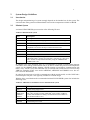
A minimal LEON/GRLIB system consists of the following IP cores:
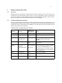
TABLE 1. Minimal LEON system
Core
Description
CLKGEN
Clock generator
RSTGEN
Reset generator. Generating a glitch free on-chip system reset signal.
AHBCTRL
AHB arbiter/controller.
APBCTRL
AHB/APB bridge/controller. Must be included in order to interface
peripheral cores such as interrupt controller and timer unit.
LEON3/4
LEON3/4 processor
IRQMP
Interrupt controller
GPTIMER
General Purpose Timer Unit
MEMCTRL
Memory controller providing access to (P)ROM and RAM. The
GRLIB IP Library contains several memory controllers. It is also possible to include on-chip ROM and RAM by using the AHBROM and
AHBRAM IP cores.
In addition to the cores described above it is recommended to include a LEON Debug Support
Unit (DSU) and a debug communication link to be able to control the processor and inspect the
system via the GRMON Debug Monitor. GRLIB contains several debug communication link
(DCL) cores. All DCL cores are controlled over an external link to make accesses on an on-chip
AHB bus. Examples of DCL cores are the AHBJTAG, AHBUART and USBDCL cores. See section 5 for more information.
In order for the processor to be able to communicate with the outside world, an 8-bit UART and a
General Purpose I/O port is also typically included in a LEON design.
With the above considerations the recommended minimal LEON/GRLIB system also includes the
following cores:
TABLE 2. Additional recommended cores for minimal LEON system
Core
Description
DSU3/4
LEON Debug Support Unit
AHBJTAG/
AHBUART/
USBDCL/
GRETH
Debug communication link. AHBJTAG provides an external JTAG
link. Other examples include AHBUART (serial UART), USBDCL
(USB), GRETH (Ethernet debug communication link is available as
part of Ethernet MAC core).
APBUART
8-bit UART
GRGPIO
General Purpose I/O Port
6
2.3
Memory Map
2.3.1 Overview
Most LEON systems use a memory map where ROM (boot PROM) is mapped at address
0x00000000 and RAM is mapped at address 0x40000000. Traditionally the AHB/APB bridge has
been mapped at 0x80000000 and peripherals such as timer, interrupt controller and UART have
been placed at fixed offsets in the APB address space. Table 3 shows the base addresses historically used in LEON systems.
TABLE 3. Peripheral base addresses, legacy systems
Base address
Description
0x80000000
LEON2 memory controller
0x80000100
Generic UART (APBUART)
0x80000200
Multi-processor interrupt controller (IRQMP)
0x80000300
Modular timer unit (GPTIMER)
Some software may not read all peripheral core base addresses from plug&play and instead
assume that some peripherals are mapped at these fixed offsets. One of the affected software packages is the BCC toolchain, where the -qambapp switch must be given in order for the produced
software to find the UART, timer and interrupt controller in case these peripherals are not mapped
at the addresses given in table 3.
The traditional memory map described above does not fit all systems. In particular one or several
large memory area (>= 1 GiB) may be difficult to place as the standard AHB decoder in GRLIB
constrains the base address of a memory area based on the memory area size. Other reasons
include that the use of AHB-to-AHB bridges that limit how the memory areas can be arranged. As
a result of this, there are several LEON/GRLIB designs with different memory maps. In order to
ease software development, this document contains some recommendations on how memory maps
should be arranged. Section 2.3.2 shows a traditional LEON/GRLIB memory map and section
2.3.3 contains recommendations on how to arrange memory maps that contains large memory
areas.
2.3.2 Typical LEON/GRLIB Memory Map
In order to use toolchains and other software distributed by Cobham Gaisler, some constraints in
the system’s memory map should be observed. A typical LEON3 system has the following memory map:
TABLE 4. Typical LEON3 memory map
Base address
Description
0x00000000
PROM
0x40000000
RAM base address. Some systems place SRAM at address 0x40000000
and SDRAM at base address 0x60000000. When SRAM is disabled the
memory controller may automatically adjust the SDRAM base address
to 0x40000000.
0x80000000
Base address of first AHB/APB bridge connecting interrupt controller,
UART(s) and timer unit.
0x90000000
Debug Support Unit register interface
7
TABLE 4. Typical LEON3 memory map
Base address
Description
0xFFF00000
AHB I/O area (if used by any core)
0xFFFFF000
Plug’n’play area (always located within AHB I/O area)
The most important areas in the table above are base addresses for ROM and RAM. The default
linker scripts make assumptions on the locations of these areas. Also, software that makes use of
the GRLIB AMBA plug’n’play areas often assume the main plug’n’play area to be located at
0xFFFFF000. The information in this area is used by software to dynamically find the addresses of
all peripherals in the system.
The location of the first AHB/APB bridge (0x80000000 in the table above) is generally of less
importance. Some legacy software may assume that the bridge is located at the specified address.
The typical memory map given above constrains the maximum size of a memory area in the
design. The GRLIB infrastructure requires that memory areas are binary aligned according to their
size. This means that a 2 GiB memory area must start on address 0x00000000 or address
0x80000000. In order to accommodate memory areas of 2 GiB some systems use variations of the
memory map as shown in table 5.
2.3.3 Memory Map in Systems That Need 2 GiB Memory Area
TABLE 5. Memory map accomodating 2 GiB main memory area
Base address
Description
0x00000000
RAM
0x80000000
Other large area, for instance PCI bridge mapping PCI memory
0xC0000000
PROM / Memory mapped IO
0xD0000000
AHB/APB bridge
0xE0000000
Debug Support Unit register interface
0xFFF00000
AHB I/O area (if used by any core)
0xFFFFF000
Plug’n’play area (always located within AHB I/O area)
The memory map in table 5 allows a 2 GiB memory map in the address range 0x00000000 0x7FFFFFFF and is supported by the toolchains supplied by Cobham Gaisler by giving an extra
switch (see the toolchain and OS documentation for details). Note that the default start address for
a LEON processor is 0x0. If the memory map above is used, the reset start address should be
changed to 0xC0000000.
Existing LEON systems use variations of the above memory map. The main difficulties that can
arise from different memory maps is that the RAM and ROM areas may collide in linker scripts
and boot loaders. It is therefore recommended that RAM is always mapped at 0x40000000 or
0x00000000 and that ROM (boot PROM area) is mapped at 0x00000000 or 0xC0000000.
Special switches may be required when building the application if RAM is mapped at
0x00000000. See toolchain documentation for details.
2.3.4 AHB I/O Area and GRLIB Plug&Play Areas
It is recommended that the default addresses are used for AHB I/O areas (determined by generic
on AHBCTRL) and GRLIB AMBA plug&play areas (determined via generics on AHBCTRL and
APBCTRL). Software scanning routines will assume that one play&play area is located at
0xFFFFF000.
8
It is possible to place the AHB I/O area and the AHB plug&play area so that it shadows another
AHB area. As an example a PCI core can be mapped at address 0xC0000000 - 0xFFFFFFFF while
the plug&play area is still reachable at offset 0xFFFFF000. While such memory maps are perfectly valid and useful for many systems it generally not recommended to let the AHB I/O or
plug&play area shadow another area as software drivers may not recognize that some of the memory area assigned to a core is essentially unreachable.
2.4
Interrupt Assignments
2.4.1 Overview
The LEON processor and interrupt controller provides 15 interrupt lines in the default configuration. Interrupt 15 is non-maskable, which leaves 14 interrupts usable for peripheral cores. The
multiprocessor interrupt controllers (IRQMP and IRQ(A)MP cores) can be extended to provide 16
additional interrupts, called extended interrupts.
The GRLIB interrupt infrastructure allows any number of cores to share the same interrupt line.
Note, however, that sharing interrupts requires that the software drivers can handle shared interrupts. Also, the time required to serve an interrupt request may be significantly prolonged if software needs to check a large number of registers in order to determine if a peripheral asserted an
interrupt.
Some operating systems place additional constraints on interrupt assignments. The subsections
below describe the requirements of each OS. The basic rules to follow in order to be able to run the
maximum amount of software can be summarized with:
1. If possible, have one dedicated interrupt for each interrupt source (no shared interrupts).
2. Configure the timer unit (GPTIMER) to have dedicated interrupts for each timer
3. Place the timer interrupts within the range 2 - 12
4. Leave interrupts lines 13 - 15 unused
The subsections below dealing with operating systems may become outdated due to changes in the
operating systems. If in doubt, please consult the OS documentation or contact Cobham Gaisler
for the latest information.
2.4.2 Linux 2.6
Interrupt 15 is used for cross-calls. Interrupt 13 is the default selection for inter-processor-interrupts (IPI). The interrupt line to be used for IPI can be selected when building the kernel and cannot be shared with peripherals.
Linux also requires that the first timer on the general purpose timer unit (GPTIMER) has a dedicated interrupt. For SMP operation the second timer must also have a dedicated interrupt line allocated.
2.4.3 RTEMS
RTEMS supports extended interrupts. Interrupt 14 is used for cross-CPU messaging in AMP systems. This interrupt is defined in leon.h: LEON3_MP_IRQ, cannot be a shared interrupt and must
be in the range 1 .. 14.
RTEMS SMP is at the time of writing not finished and requirements are not known.
Timer 0 of GPTIMER 0 is the system clock timer, however RTEMS can be used without a timer.
There are two cases depending on which RTEMS distribution that is used:
Classical/official RTEMS BSP: GPTIMER0.timer0 must have separate IRQ and the interrupt must
be in the range 1 .. 14.
“Driver manager BSP” (RCC LEON3/4 BSP): Can handle both separate and shared IRQs on
GPTIMER, interrupt can be in the range 1 .. 31 (no limitations).
9
2.4.4 VxWorks
VxWorks makes use of interrupt 14 for inter-processor-interrupts (IPI). This interrupt should not
be shared with peripherals.
2.5
Device Specific Identification
GRLIB systems have two identifiers in the system’s plug&play area that can be used to distinguish
a particular device: The GRLIB build ID and the GRLIB System Device ID. The GRLIB build ID
is set globally for the full library and the device ID is set per design via the AHBCTRL VHDL
generic devid (refer to the AHBCTRL section in GRLIB IP Core User’s Manual, grip.pdf). This
VHDL generic should be set to a unique value for all new designs. The file lib/grlib/amba/
devices.vhd lists device IDs, under the comment grlib system device id’s, used for some existing
designs. It is recommended that customer designs use an ID larger than 16#0a00#. Please contact
Cobham Gaisler support if you wish to have you device ID added to the listing in devices.vhd.
Communication interfaces may have additional vendor and device identifiers. This is, for instance,
the case for JTAG, PCI and USB. For the USB debug link it is recommended that users keep the
Cobham Gaisler IDs so that GRMON may properly detected the debug link. For all other identifiers the implementers of a device should use their own IDs as assigned by the appropriate organisations. Re-use of Cobham Gaisler’s vendor/manufacturer ID may prevent the device from fully
functioning together with software and debug tools.
10
3
LEON design information
3.1
Introduction
The sections below contain recommendations on how to configure the LEON processors depending on system requirements.
3.2
General Recommendations
3.2.1 SPARC V9 CASA
The LEON4 processor and later revisions of the LEON3 processor contain support for the SPARC
V9 CASA instruction. It is recommended that all new LEON3 implementations include support
for CASA (this is a strict requirement if the system will run WindRiver VxWorks in SMP).
3.2.2 Data Cache Snooping
To keep the data cache synchronized with external memory, cache snooping can be enabled. When
enabled, the data cache monitors write accesses on the AHB bus to cacheable locations. If another
AHB master writes to a cacheable location that is currently cached in the date cache, the corresponding cache line is marked as invalid.
Data cache snooping is of high importance for SMP systems and, in general, both simplifies and
increases performance in systems with multiple masters. Note that the processor(s) snoop on the
bus to which they are directly connected. In a system with multiple AHB buses, snooping will only
work on the bus to which the processors are connected. Snooping will not provide cache coherency if, for instance, there are masters connected between a Level-2 cache and memory, while the
processors are located in front of the Level-2 cache.
If the processor(s) is implemented with a memory management unit (MMU), then extra physical
tags must be enabled.
3.2.3 V7 and FPU
When the LEON is implemented with an FPU it should also include hardware support for multiply
and divide (SPARC V8 MUL/DIV selected with the LEON VHDL generic v8). Otherwise a
SPARC V7 processor with FPU will be obtained and this configuration may not be supported by
prebuilt packages and toolchains.
3.3
LEON Example Configurations
3.3.1 Overview
The subsections below show three different example configurations for LEON processors; a minimal configuration used to target low area and high frequency, a typical configuration with all features enabled, and a high-performance configuration where the requirements on processing
performance outweigh area and power considerations.
Each section contains a table with recommended values for some of the LEON processor VHDL
generics. If you are using the xconfig GUI to configure the processor then please not that the
VHDL generic names do not directly correspond to the configuration options in the GUI. The
descriptions of the configuration settings should provide enough information to do appropriate
configuration selection also via xconfig. The xconfig tool also has support to initialize the processor configuration with values from the three example configurations described in the sections
below. See the configuration help text in xconfig for the option Force values from example configuration in the Processor sub menu for additional information.
11
Also note that all listed configuration options do not apply to all LEON processors. For instance,
the LEON3 processor has a VHDL generic called bp that controls the inclusion of branch predication, while the LEON4 processor is always implemented with support for branch prediction.
3.3.2 Minimal LEON Configuration
This LEON configuration is aimed at resource constrained systems where the area requirements of
the processor core needs to be minimized. Note that using an area minimized configuration may
not necessarily reduce the system’s performance since it may be possible to achieve a higher operating frequency by reducing the amount of logic in the processor core.
Table 6 below shows recommended values for some of the LEON processor VHDL generics to
attain a minimal configuration in terms of area.
TABLE 6. Minimal LEON processor configuration
VHDL
generic
Recommended
value
dsu
0
Some area can be saved by removing the Debug Support Unit
(DSU). However, this unit can prove to be invaluable at least during the software development phase.
fpu
0
Disable floating-point unit
v8
0
Do not include support for SPARC V8 MUL/DIV instructions
mac
0
Do not include support for SPARC V8e SMAC/UMAC
nwp
0
Disable hardware watchpoints
icen / dcen
1
Include processor caches
isets / dsets
1
Direct mapped instruction and data cache
irepl / drepl
2
Random replacement policy for both instruction and data cache
isetsize /
dsetsize
-
The size of the caches does not significantly affect the required
logic. Choose cache size according to application requirements
and amount of RAM available on target device.
dnsoop
0
Disable data cache snooping (see section 3.2.2)
mmuen
0
Disable memory management unit (MMU). Note: May be required
depending on software applications.
lddel
1
1-cycle load delay
tbuf
0
Disable instruction trace buffer (NOTE: Including the instruction
trace buffer may be of high value during software development and
debug).
pwd
1
Power-down implementation. Choose 2 if frequency target is not
met.
smp
0
Disable SMP support. If the processor core should be used in an
SMP configuration then see the GRIP documentation on how to set
the SMP generic. If SMP is enabled then the dsnoop VHDL
generic should also be set accordingly.
bp
0
Disable branch prediction
Description
12
3.3.3 General Purpose LEON Configuration
This LEON configuration is aimed for general purpose processing balancing performance against
area and power requirements.
TABLE 7. General purpose LEON processor configuration
VHDL
generic
Recommended
value
Description
dsu
1
Include support for the LEON Debug Support Unit (DSU)
fpu
-
Include floating-point unit based on application requirements. A
floating-point unit is highly recommended for most systems.
LEON processors can primarily interface the GRFPU or GRFPUlite floating point unit. The GRFPU is a high-performance pipelined FPU with high area requirements. GRFPU-lite provides a
balanced option with high acceleration of floating-point computations combined with lower area requirements compared to
GRFPU.
v8
2
Include support for SPARC V8 MUL/DIV instructions using a 5cycle multiplier. Note that if the target technology has multiplier
blocks a single-cycle multiplier (v8 generic set to 1) may provide
lower area and higher performance.
mac
0
Do not include support for SPARC V8e SMAC/UMAC instructions.
nwp
2
Include two hardware watchpoints
icen / dcen
1
Include processor caches.
isets / dsets
2
Implement instruction and data caches with two ways
irepl / drepl
2
Random replacement policy for both instruction and data cache, or
possibly LRU replacement (irepl/drepl set to 0).
isetsize /
dsetsize
-
The size of the caches does not significantly affect the required
logic. Choose cache size according to application requirements
and amount of RAM available on target device.
dnsoop
6
Enable snooping with extra physical tags (see section 3.2.2)
mmuen
1
Enable memory management unit (MMU)
itlbnum /
dtlbnum
8
Use eight entries each for the instruction and data MMU translation look-a-side buffers
tlb_type
2
Use separate translation look-a-side buffers (TLB) with fast write
for data and instruction.
tlb_rep
0
Use LRU TLB replacement
lddel
1
Use 1-cycle load delay
tbuf
4
Use 4 KiB instruction trace buffer.
pwd
2
Timing efficient power-down implementation.
smp
0
Disable SMP support. If the processor core should be used in an
SMP configuration then see the GRIP documentation on how to set
the SMP generic.
bp
1
Enable branch prediction
13
3.3.4 High Performance LEON Configuration
This LEON configuration is aimed at high performance processing where the needs for computational speed outweighs area and power requirements.
In order to reduce the effects of memory latency, a Level-2 cache is recommended for high-performance systems. This is of particular interest in multiprocessor systems.
TABLE 8. High-performance LEON processor configuration
VHDL
generic
Recommended
value
Description
dsu
1
Include support for the LEON Debug Support Unit (DSU)
fpu
1-7
Use GRFPU floating-point unit. Select (FP) multiplier depending
on target technology. For FPGA this would typically be inferred
(1) or technology specific (4). For ASIC DesignWare multiplier (2)
or Module Generator (3).
v8
16#32#
Include support for SPARC V8 MUL/DIV instructions using a
32x32 pipelined multiplier. Note that if the target technology has
multiplier blocks a single-cycle multiplier (v8 generic set to 1)
may provide lower area and higher performance.
mac
0
Do not include support for SPARC V8e SMAC/UMAC instructions
nwp
4
Include support for four hardware watchpoints
icen / dcen
1
Include processor caches.
isets / dsets
2
Implement instruction and data caches with two ways
irepl / drepl
0
Least-Recently-Used replacement policy for instruction and data
caches.
isetsize /
dsetsize
-
The size of the caches does not significantly affect the required
logic. Choose cache size according to application requirements
and amount of RAM available on target device.
dnsoop
6
Enable snooping with extra physical tags (see section 3.2.2)
mmuen
1
Enable memory management unit (MMU)
itlbnum /
dtlbnum
16
Use sixteen entries each for the instruction and data MMU translation look-a-side buffers
tlb_type
2
Use separate translation look-a-side buffers (TLB) with fast write
for data and instruction.
tlb_rep
0
Use LRU TLB replacement
lddel
1
Use 1-cycle load delay
tbuf
4
Use 4 KiB instruction trace buffer.
pwd
2
Timing efficient power-down implementation.
smp
>0
Enable SMP support. If the processor core should be used in an
SMP configuration then see the GRIP documentation on how to set
the SMP generic. Note that several processor entities must be
instantiated. This configuration option only enables support for
SMP, it does not instantiate several processor cores.
bp
1
Enable branch prediction
14
4
Multiple Buses, Clock Domains and Clock Gating
4.1
Introduction
This section describes some techniques that can be used with GRLIB to create more complex system architectures with multiple buses and/or clock domains.
Peripheral IP cores that need to work at a separate clock domain usually have their own clocking
and synchronization built in. This is not explained here, see the core-specific documentation.
4.2
Creating Multi-Bus Systems
4.2.1 Overview
The on-chip bus may become a bottle neck in systems where the processors and peripherals all
share the same bus. The fact that all IP cores are connected together may also introduce high loads
in the system, which can lead to timing issues at implementation. These issues can be solved by
partitioning the system into several AHB buses.
4.2.2 GRLIB Facilities
In order to partition the system into multiple buses, the general-purpose AHB bridge IP cores
AHBBRIDGE (uni-directional) and AHB2AHB (bi-directional) are included in GRLIB. There are
also special-purpose cores, such as the IOMMU and L2-cache, that have bridge functionality built
into them.
4.2.3 GRLIB AMBA Plug&Play in Multi-Bus Systems
Software and debug monitors such as GRMON can detect all IP cores connected to the on-chip
bus(es) by scanning the plug&play configuration area. The format and function of this area is
described in the GRLIB User’s Manual and in the GRLIB IP Core User’s Manual documentation
for the AHB controller (AHBCTRL) and AHB/APB bridge (APBCTRL).
In multi-bus systems, each bus will have its own AMBA plug&play configuration area and software must be able to access all plug&play areas In order for software able to discover all peripherals in a system. The same applies for the GRMON debug monitor, to discover all peripherals the
debug communication link master interface must be connected to a bus from where it can access
all plug&play areas (as well as memory where peripheral registers are mapped).
The plug&play scanning routines discover the presence of multiple AHB buses when it discovers
the slave interface a core such as the Level-2 cache or AHB/AHB bridge (AHB2AHB, AHBBRIDGE). Upon discovery of a bridge the routine will typically look in the user defined register of
the bridge’s plug&play information to get the base address of the AHB I/O and plug&play area of
the second bus. Excatly how the base address of the plug&play information is communicated to
the scanning routine is specific for each core. The Level-2 cache and AHB/AHB bridges store this
address in user defined register 1 of the core’s AHB slave interface plug&play information. A
value of zero in this register signals to software that plug&play scanning should not be done for the
second bus behind the bridge.
When software discovers a bridge to a new bus, scanning should commence using the new
plug&play area address (depth-first scanning) and once the new plug&play area has been handled
scanning should continue on the current bus.
Note that for plug&play scanning to work, all plug&play areas must be accessible from the AHB
master that performs the scan. This means that any bridge between AHB buses must have a window that allows the plug&play area on the other side of the bridge to be accessed. System software
and debug tools by default start scanning for a plug&play area at the top of AMBA memory space.
it is important that the plug&play area located in this address has pointers so that all other
plug&play areas in the system can be discovered. For instance, the default plug&play area address
should not be occupied by the plug&play area of a bus that is only connected to the rest of the sys-
15
tem via the AHB master interface side of a Level-2 cache or uni-directional bridge. This is because
the extra information at the AHB master interface does not contain the base address for the
plug&play area of the bus on the AHB slave interface side of the bridge. As a result of this,
plug&play scanning routines will only find one bus in the system.
4.2.4 Buses in Different Clock Domains
In order to work around timing issues, or to reduce power consumption, it can make sense to partition the design also into several clock domains. The AHB/AHB bridges (AHB2AHB, AHBBRIDGE and GRIOMMU) allows connecting buses with differing operating frequencies together.
The bus clocks on each side of the bridge need to have a frequency ratio relationship and fixed
phase relation. This avoids the need to resynchronize signals on chip which would cause a performance penalty.
If you want to run everything except the processor at half speed, a more efficient solution than
using bridges is to use the LEON double clocking support explained in section 4.3.
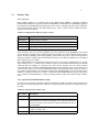
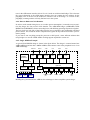
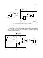
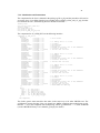
4.2.5 Single AHB Bus Example
A typical LEON/GRLIB design is shown in the figure below. The design is centered around one
AMBA AHB bus and also has a AMBA APB bus that connects some of the peripheral cores via an
AHB/APB bridge.
USB PHY
USB
LEON3
Processor
RS232
JTAG
PHY
LVDS
CAN
Serial
Dbg Link
JTAG
Dbg Link
Ethernet
MAC
Spacewire
Link
CAN 2.0
Link
AMBA AHB
AHB
Controller
Memory
Controller
AMBA APB
AHB/APB
Bridge
I/O port
PS/2
UART
Timers
RS232
WDOG
IrqCtrl
VGA
8/32-bits memory bus
PROM
I/O
SDRAM
16-bit I/O PS/2 IF
port
Video
DAC
Building the system around one AHB bus has advantages in that it simplifies system design.
16
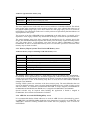
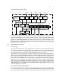
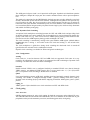
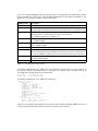
4.2.6 Multi-Bus System Example
LEON3
Processor
AHB
Controller
RS232
JTAG
PHY
LVDS
CAN
Serial
Dbg Link
JTAG
Dbg Link
Ethernet
MAC
Spacewire
Link
CAN 2.0
Link
AMBA AHB
Memory
Controller
AHB2AHB
Bridge
AMBA APB
AHB/APB
Bridge
I/O port
PS/2
UART
Timers
IrqCtrl
SVGA
(SVGA) AMBA AHB
Memory
Controller
AHB
Controller
One example (shown above) of when a multi-bus system resolves bus contention is when a SVGA
controller (SVGACTRL core) is used. The SVGA controller continuously reads a frame buffer
located in external memory. This constant data fetching can consume a significant amount of the
available bus bandwidth, particularly in systems with relatively low system frequencies. The
impact of the SVGA controller bus traffic can be removed by placing the SVGA controller and a
dedicated memory controller on a separate bus. The processor can still access the frame buffer
through and uni-directional bridge.
4.3
LEON3 Double-Clocking
4.3.1 Overview
To avoid critical timing paths in large AHB systems, it is possible to clock the LEON3 processor
core at an inter multiple of the AHB clock. This will allow the processor to reach higher performance while executing out of the caches. This chapter will describe how to implement a LEON3
double-clocked system using the LEON3-CLK2X template design as an example.
The LEON3 CPU core be clocked at a multiple of the the clock speed of the AMBA AHB bus.
When clocked at double AHB clock frequency, all CPU core parts including integer unit and
caches will operate at double AHB clock frequency while the AHB bus access is performed at the
slower AHB clock frequency. The two clocks have to be synchronous and a multicycle paths
between the two clock domains have to be defined at synthesis tool level. Separate components
(leon3s2x, leon3x, leon3ft2x) are provided for the double clocked core. Double clocked versions
of DSU (dsu3_2x) and MP interrupt controller (irqmp2x) are used in a double clocked LEON3
system. An AHB clock qualifier signal (clken input) is used to identify end of AHB cycle. The
AHB qualifier signal is generated in CPU clock domain and is high during the last CPU clock
cycle under AHB clock low-phase.
4.3.2 LEON3-CLK2X Template Design
The LEON3-CLK2X design is a multi frequency design based on double-clocked LEON3 CPU
core. The LEON3 CPU core and DSU run at multiple AHB frequency internally, while the AHB
bus and other AHB components are clocked by the slower AHB clock. Double clocked version of
17
the interrupt controller is used, synchronizing interrupt level signals between the CPU and the
interrupt controller.
The design can be configured to support different ratios between CPU and AHB clock such as 2x,
3x or 4x. If dynamic clock switching is enabled, an glitch-free clock multiplexer selecting between
the fast CPU clock and the slower AHB clock is used to dynamically change frequency of the CPU
core (by writing to an APB register).
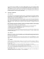
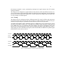
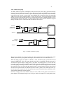
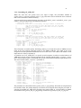
4.3.3 Clocking
The design uses two synchronous clocks, AHB clock and CPU clock. For Xilinx and Altera technologies the clocks are provided by the clkgen module, for ASIC technologies a custom clock generation circuit providing two synchronous clocks with low skew has to be provided.
An AHB clock qualifier signal, identifying end of an AHB clock cycle is necessary for correct
operation of the double-clocked cores. The AHB clock qualifier signal (HCLKEN), indicating end
of an AHB clock cycle, is provided by the qmod module. The signal is generated in CPU clock
domain and is active during the last CPU clock cycle during low-phase of the AHB clock. Figure 1
shows timing for CPU and AHB clock signals (CPUCLK, HCLK) and AHB clock qualifier signal
(HCLKEN) for clock ratios 2x and 3x.
CPUCLK
HCLK
HCLKEN
CPUCLK
HCLK
HCLKEN
Figure 1. Timing diagram for CPUCLK, HCLK and HCLKEN
18
4.3.4 Multicycle Paths
Paths going through both CPU and AHB clock domains have propagation time of one AHB clock
cycle, and should be marked as multicycle paths with following exceptions:
Start point
Through
End point
Propagation time
CPUCLK
ahbi
CPUCLK
N CPUCLK
CPUCLK
ahbsi
CPUCLK
N CPUCLK
CPUCLK
ahbso
CPUCLK
N CPUCLK
HCLK
irqi
CPUCLK
1 CPUCLK
CPUCLK
irqo
HCLK
1 CPUCLK
u0_0/p0/c0/sync0/r[*]
(register)
1 CPUCLK
leon3s2x core
CPUCLK
dsu3_2x core
CPUCLK
ahbmi
CPUCLK
N CPUCLK
CPUCLK
ahbsi
CPUCLK
N CPUCLK
dsui
CPUCLK
1 CPUCLK
rh[*] (register)
1 CPUCLK
r[*] (register)
1 CPUCLK
r[*] (register)
irqmp2x core
r2[*] (register)
* N is ratio between CPU and AHB clock frequency (2, 3, ...)
Sample DC script defining multicycle paths and exceptions is provided in the design directory
(dblclk.dc).
Figure 2 shows synchronization of AHB signals starting in HCLK clock domain and ending in
CPUCLK domain (inside the double clocked cores LEON3S2X and DSU3_2X). These AHB signals are captured by registers in CPUCLK domain at the end of AHB clock cycle, allowing propagation time of 2 or more CPUCLK cycles (one HCLK cycle). The end of the AHB clock cycle is
indicated by the AHB clock qualifier signal HCLKEN. One of the inputs of the AND gate in figure
below is connected to the clock qualifier signal HCLKEN ensuring that the value of the signal
AHBI is latched into R2 at the end of AHB cycle (HCLKEN = ‘1’). The value of signal AHBI is
not valid in the CPUCLK clock domain if the qualifier signal HCLKEN is low. In this case, the
AND gate will be closed and the value of the signal AHBI will not propagate to register R2.
19
HCLK
Clock Domain
CPUCLK
Clock Domain
R1
R2
AHBI
D
Q
D
D
Q
Q
HCLKEN CPUCLK
HCLK
CPUCLK
LEON3S2X
Figure 2. Synchronization between HCLK and CPUCLK clock domains
Synchronization of AHB signals going from the double clocked cores to the AHB clock domain is
shown if figure 3. The AND gate is open when CPU (or DSU) performs an AHB access (AHBEN
= ‘1’). When the AND gate is open, the signal AHBO will be stable during the whole AHB cycle
and its value propagates to the HCLK clock domain (AHB bus). When CPU does not perform
AHB access (CLKEN = ‘1’) the AND gate is closed (AHBEN = ‘0’) disabling propagation of signal AHBO to the HCLK clock domain.
CPUCLK
Clock Domain
HCLK
Clock Domain
R1
D
AHBO
Q
R2
D
CPUCLK
D
Q
AHBEN
HCLK
HCLK
LEON3S2X
Figure 3. Synchronization between CPUCLK and HCLK clock domains
Q
20
The AND gates in figures 2 and 3 are 2-input clock AND gates. Synthesis tool should not optimize
these AND gates. Sample DC-script puts ‘don’t-touch’ attribute on these cells to prevent optimization.
The multicycle constraints for the GRLIB double clocked cores are typically defined by start clock
domain, intermediate points and end clock domain. Although FPGA synthesis tools provide support for multicycle paths, they do not provide or have limited support for this type of multicycle
constraints (start clock domain, intermediate points, end clock domain). This limitation results in
over-constrained FPGA designs (multicycle paths become single cycle) which are fully functional
and suitable for FPGA prototyping.
4.3.5 Dynamic Clock Switching
An optional clock multiplexer switching between the CPU and AHB clocks and providing clock
for double-clocked cores can be enabled. The clock multiplexer is used to dynamically change frequency of the CPU core, e.g. CPU can run at lower AHB frequency during periods with low CPU
load and at twice the AHB frequency during periods with high CPU load.
The clock switching is controlled by writing to the qmod modules APB register (default address
0x80000400), bit 0: writing ‘1’ will switch to the CPU clock and writing ‘0’ will switch to the
AHB clock.
The clock multiplexer is glitch-free, during clock switching the deselected clock is turned-off
(gated) before the selected clock is enabled and selected.
Dynamic clock switching is available for Xilinx and generic technologies.
4.3.6 Configuration
xconfig
Clock ratios 2x, 3x and 4x between CPU and AHB clock are supported. Clock ratio 2x is supported for all technologies, ratios 3x and 4x are supported for ASIC technologies. Dynamic clock
switching is available for Xilinx and ASIC technologies.
leon3s2x
Double-clocked LEON3 core is configured similarly to standard LEON3 core (leon3s) through
VHDL generics. An additional VHDL generic clk2x is set to ((clock ratio - 1) + (8 * dyn)) where
dyn is 1 if dynamic clock switching is enabled and 0 if disabled.
qmod
Local qmod module generates AHB clock qualifier signal and optionally controls dynamic clock
switching. The module is configured through VHDL - generics defining clock ratio (clkfact),
dynamic clock switching (dynfreq) and address mapping of modules APB register (pindex, paddr,
pmask).
irqmp_2x
VHDL generic clkfact should be set to clock ratio between CPU and AHB clocks.
4.4
Clock gating
4.4.1 Overview
GRLIB contains support for using clock gating for both the processors and peripheral IP cores.
The GRCLKGATE unit described in the GRLIB IP Core User’s Manual can be used both to gate
peripherals and to provide automatic processor (and floating-point unit) clock gating.
21
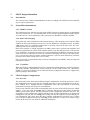
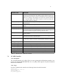
4.4.2 LEON clock gating
To further reduce the power consumption of the processor, the clock can be gated-off when the
processor has entered power-down state. Since the cache controllers and MMU operate in parallel
with the processor, the clock cannot be gated immediately when the processor has entered the
power-down state. Instead, a power-down signal (DBGO.idle) is generated when all outstanding
AHB accesses have been completed and it is safe to gate the clock. This signal should be clocked
though a positive-edge flip-flop followed by a negative-edge flip-flop to guarantee that the clock is
gated off during the clock-low phase. To ensure proper start-up state, the clock should not be gated
during reset and at least 3 clocks after that reset has been de-asserted.
LEON3/4 entity
RESETN
DBGO.IDLE
DBGO.IPEND
D
Q
D
Q
GCLK
CLK
AHB CLK
LEON3/4 entity
RESETN
DSUO.PWD[n]
D
Q
GCLK
CLK
AHB CLK
Figure 4. Examples of LEON clock gating
The processor should exit the power-down state when an interrupt become pending. The signal
DBGO.ipend will then go high when this happen, and should be used to re-enable the clock.
When the debug support unit (DSU3 or DSU4) is used, the DSUO.pwd signal should be used
instead of DBGO.idle. This will ensure that the clock also is re-enabled when the processor is
switched from power-down to debug state by the DSU. The DSUO.pwd is a vector with one
power-down signal per CPU (for SMP systems). DSUO.pwd takes DBGO.ipend into account, and
no further gating or latching needs to be done of this signal. If cache snooping has been enabled,
the continuous clock will ensure that the snooping logic is activated when necessary and will keep
the data cache synchronized even when the processor clock is gated-off. In a multi-processor system, all processor except node 0 will enter power-down after reset and will allow immediate clockgating without additional software support.
Clock-tree routing must ensure that the continuous clock (CLK) and the gated clock (GCLK) are
phase-aligned. The template design leon3-clock-gate shows an example of a clock-gated system.
22
Please refer to the LEON signal descriptions in the GRLIB IP Core User’s Manual document for
documentation on which processor clock inputs that are allowed to be gated-off. Please also see
the documentation for the GRCLKGATE and GRCLKGATE2 IP cores in the same document.
23
5
Debug communication links
5.1
Overview
GRLIB contains several debug communication link (DCL) controller cores. All DCL cores are
controlled over an external link to make accesses on an on-chip AHB bus. These communcation
links can be used by an external debug monitor to perform debugging operations on the system or
by other external devices that need direct memory access to the design.
5.2
Available debug link controllers
A debug communication link controller is an IP core that has that supports communication over an
external interface without on-chip software involvement. The IP core decodes incoming traffic and
translates the traffic to operations on the AMBA bus. The table below lists IP cores that can act as
debug communication link controllers.
TABLE 9. Debug Communication Link controllers
Interface
IP core
AMBA access
size supported
Notes
Serial UART
AHBUART
Word
Supported by GRMON
JTAG
AHBJTAG
Byte, Half-word,
Word
Supported by GRMON
Ethernet
GRETH /
Word
DCL functionality is optional to include in
Ethernet controllers. Supported by
GRMON.
GRETH_GBIT
PCI
GRPCI / GRPCI2
Byte, Half-word,
Word
GRMON can make use of PCI target to
access system.
SpaceWire
RMAP
GRSPW
GRSPW2 /
Read: Byte,
Half-word, Word
GRSPWROUTER
Write: Word
RMAP hardware handler is optional to
include in SpaceWire controllers. GRMON
can connect via GRESB Ethernet-toSpaceWire bridge. The controllers translate
subword write accesses to 32-bit read-modify-write operations.
USB
GRUSB_DCL
Word
Supported by GRMON
I2C
I2C2AHB
Byte, Half-word,
Word
Not supported by GRMON
SPI
SPI2AHB
Byte, Half-word,
Word
Not supported by GRMON
24
6
Core specific design recommendations
6.1
Overview
The subsections below contain system design recommendations when using specific GRLIB
cores.
6.2
AHB/AHB Bridges (AHB2AHB/AHBBRIDGE/GRIOMMU)
The AHB/AHB bridges can be of high value when partitioning the system into several clock
domains or when there is a need to separate bus traffic. The use of a bridge will result in increased
latencies when accesses need to traverse over the bridge.
For bi-directional bridge configurations the designer needs to be aware that collisions (attempts to
traverse the bridge both ways simultaneously) will mean that the access on the slave bridge will be
aborted and then re-attempted. This situation can potentially lead to starvation and deadlocks.
When instantiating the bridge with a prefetch buffer the buffer should be scaled so that it does not
prefetch unnecessarily large amounts of data. If the master(s) traversing the bridge have a maximum burst length of eight words, then the bridge’s prefetch buffer should not be larger than eight
words.
6.3
SVGA Controller (SVGACTRL)
The SVGA controller can consume a significant amount of the available bus bandwidth. Even if
calculations show that there is plenty of bandwidth available, the inclusion of SVGACTRL may
add bus access latencies that significantly impact computational performance. For design that
include a SVGA controller it is recommended to place the SVGA controller on a separate bus with
a dedicated frame buffer memory.
25
7
GRLIB AMBA Test Framework
7.1
Overview
GRLIB has a number of packages that can aid in verification of AMBA cores. New developments
should use the GRLIB AMBA Test Framework (ATF). The test framework consists of an AHB
master core, an AHB slave core and an AHB arbiter/controller core. The AHB master and slave
cores have debug interfaces that allow them to be controlled using external stimuli.
The sections below give an overview of the components in the framework. The test framework is
not distributed as a product and there is no complete user’s manual. The test master and slave is
controlled by procedure calls that are documented in their respective VHDL packages (described
below).
ATF files are located in the directory <grlib root>/lib/grlib/atf/. All GRLIB distributions do not
include ATF. If the atf directory is missing from your GRLIB tree, then your version of GRLIB
does not contain the components described in this section.
NOTE: The GRLIB AMBA test framework is NOT included in the free GRLIB-GPL.
7.2
AT AHB Master
7.2.1 Description
The AT AHB Master (AT_AHB_MST) is a non-synthesizable AHB master core with a debug
interface so that the master can be controlled via function calls.
7.2.2 Initialization and Instantiation
The component for the master is defined in the package grlib.at_pkg and the procedure calls to
control the master is available in the package grlib.at_ahb_mst_pkg. In order to instantiate the
master, the following libraries should be included:
library ieee;
use ieee.std_logic_1164.all;
library grlib;
use grlib.amba.all;
use grlib.at_pkg.all;
use grlib.at_ahb_mst_pkg.all;
use grlib.testlib.all;
The component for AT_AHB_MST has the following interface:
component at_ahb_mst is
generic(
hindex:
in
Integer := 0;
vendorid:
in
Integer := 0;
deviceid:
in
Integer := 0;
version:
in
Integer := 0;
grlibdatamux: in
integer := 1);
port(
-- AMBA AHB system signals
hclk:
in
std_ulogic;
hresetn:
in
std_ulogic;
--AHB Interface
ahbi:
in
ahb_mst_in_type;
ahbo:
out
ahb_mst_out_type;
--Operation Scheduling Interface
atmi:
in at_ahb_mst_in_type;
atmo:
out at_ahb_mst_out_type
);
end component;
The only VHDL generics that require proper assignment are hindex and grlibdatamux. The hindex
generic must match the bus index in the same way as for other GRLIB AHB masters. The grlibdatamux generic decides if the core should use AMBA compliant data multiplexing (grlibdatamux
=> 0) or the simplified data multiplexing scheme (grlibdatamux => 1) commonly used in GRLIB
26
(see the GRLIB IP Library User’s Manual, grlib.pdf, for details). For use in a normal GRLIB system the default value is recommended. An example instantiation of AT_AHB_MST can be found
in verification/at/at_tb.vhd. At the top of the file the libraries mentioned above are included. The
test bench instantiates several AMBA masters, the signals used to control the debug interfaces are
created as:
signal atmi
signal atmo
: at_ahb_mst_in_vector(0 to 2);
: at_ahb_mst_out_vector(0 to 2);
The masters are then instantiated using a generate loop:
-- Masters
mstrs01 : for i in 0 to 2 generate
amst : at_ahb_mst
generic map(
hindex
=> FIRST_MASTER_INDEX+i,
vendorid
=> 0,
deviceid
=> 0,
version
=> 0)
port map(
-- AMBA AHB system signals
hclk
=> clk,
hresetn
=> rstn,
-- Direct Memory Access Interface
atmi
=> atmi(i),
atmo
=> atmo(i),
-- AMBA AHB Master Interface
ahbi
=> ahbmi,
ahbo
=> ahbmo(FIRST_MASTER_INDEX+i));
end generate;
The masters are controlled by calls from the test bench process. Before use, each master debug
interface must be initialized. In verification/at/at_tb.vhd this is done by calls to at_init(..):
testbench: process
----- variable definitions removed ----begin -- process testbench
---------------------------------------------------------------------------- Testbench initialization
--------------------------------------------------------------------------Print("----------------------------------------------");
Print("AMBA Test Framework test bench");
Print("----------------------------------------------");
for i in atmi'range loop
at_init(i, atmi);
end loop;
wait until rstn = '1'
7.2.3 Simple Accesses
After initalization has been performed, as described in the previous section, the procedures defined
in grlib.at_ahb_mst_pkg (lib/grlib/atf/at_ahb_mst_pkg.vhd) can be used to command the master to
perform accesses. The procedures are either read or write procedures. A read or write procedure
can be either blocking (call will not return before the access is completed) or non-blocking (call
will return immediately and another call must be made at a later time in order to complete the command on the debug interface). All non-blocking procedures have names ending with _nb, the procedures used to complete a non-blocking call have names that end with _nb_fin.
Procedures that make single accesses are named in the following format: at_read_<size>(..) or
at_write_<size>(..). Where <size> can be 8, 16, 32, 64, 128 or 256. The non-blocking pairs are
named at_read_<size>_nb(..) / at_read_<size>_nb_fin(..) and at_write_nb(..) /
at_write_nb_fin(..). There are also procedures that make burst accesses. These have the word burst
in their name, for instance at_write_burst_32(..). The procedure names are overloaded and there
can be several variants of a procedure, with a different number of parameters.
The simplest way to perform a single access, in this case a write, is to use a call like:
27
at_write_32(
address => X”h40000000”,
data => X”01234567”,
atmi => atmi(0),
atmo => atmo(0));
The non-blocking variant is (here we assume that we have defined the variable id as an integer and
the variable ready as a boolean):
at_write_32_nb(
address => X”h40000000”,
data => X”01234567”,
waitcycles => 0,
lock => false,
hprot => “0011”,
back2back => false,
screenoutput => false,
id => id,
atmi => atmi(0),
atmo => atmo(0));
-- Here other tasks can be performed
at_write_32_nb_fin(
id => id,
wait_for_op => true,
screenoutput => false,
ready => ready,
atmi => atmi(0),
atmo => atmo(0));
The first call initiates a write access to address 0x40000000 with data 0x01234567. The access
should start immediately, not assert HLOCK and use the specified HPROT (0b0011). The first call
will assign an access identifier to the variable id. This identifier is used by AT_AHB_MST to keep
track of the access. The same access identifier must then be used in the call to
at_write_32_nb_fin(..). The core will try to perform the write access even if the call to
at_write_32_nb_fin(..) never takes place. However, if at_write_32_nb_fin(..) is never called, the
core will keep a record of the completed access in its internal data structures forever.
A call to at_<operation>_<size>_nb_fin(..) procedure will block if the wait_for_op parameter is
set to true. If wait_for_op is set to false, the call will return immediately and the ready variable
must be checked to see if AT_AHB_MST completed the access.
The description given for write operations above also applies to read operations. Note that for nonblocking reads (at_read_<size>_nb(..) / at_read_<size>_nb_fin(..)), the data will be returned
when at_read_<size>_nb_fin(..) is called. The first call only tells the master to initiate an access,
the at_read_<size>_nb_fin(..) call will tell you when, and if, the access has completed and the
master will have data available.
As mentioned above, the core can also generate burst accesses. In the case of non-blocking burst
accesses, the id and ready parameters will be arrays instead of single values.
The description above covers basic operation of AT_AHB_MST. Please refer to the
grlib.at_ahb_mst_pkg package located at lib/grlib/atf/at_ahb_mst_pkg.vhd to see all available procedure calls. Each call and its parameters are documented in the package.
7.3
AT AHB Slave
7.3.1 Description
The AT AHB Slave (AT_AHB_SLV) is an non-synthesizable AHB slave core with a debug interface that allows insertion of custom AHB replies and access to the core’s internal memory structures.
28
7.3.2 Initialization and Instantiation
The component for the slave is defined in the package grlib.at_pkg and the procedure calls used to
access the slave via its debug interface are available in the package grlib.at_ahb_slv_pkg. In order
to instantiate the slave, the following libraries should be included:
library ieee;
use ieee.std_logic_1164.all;
library grlib;
use grlib.amba.all;
use grlib.at_pkg.all;
use grlib.at_ahb_slv_pkg.all;
The component for AT_AHB_SLV has the following interface:
component at_ahb_slv is
generic (
hindex
: integer := 0;
bank0addr
: integer := 0;
bank0mask
: integer := 0;
bank0type
: integer := 0;
bank0cache
: integer := 0;
bank0prefetch : integer := 0;
bank0ws
: integer := 0;
bank0rws
: integer := 0;
bank0dataload : integer := 0;
bank0datafile : string := "none";
bank1addr
: integer := 0;
bank1mask
: integer := 0;
bank1type
: integer := 0;
bank1cache
: integer := 0;
bank1prefetch : integer := 0;
bank1ws
: integer := 0;
bank1rws
: integer := 0;
bank1dataload : integer := 0;
bank1datafile : string := "none";
bank2addr
: integer := 0;
bank2mask
: integer := 0;
bank2type
: integer := 0;
bank2cache
: integer := 0;
bank2prefetch : integer := 0;
bank2ws
: integer := 0;
bank2rws
: integer := 0;
bank2dataload : integer := 0;
bank2datafile : string := "none";
bank3addr
: integer := 0;
bank3mask
: integer := 0;
bank3type
: integer := 0;
bank3cache
: integer := 0;
bank3prefetch : integer := 0;
bank3ws
: integer := 0;
bank3rws
: integer := 0;
bank3dataload : integer := 0;
bank3datafile : string := "none";
grlibdatamux : integer := 1
);
port (
rstn : in std_ulogic;
clk
: in std_ulogic;
ahbsi : in ahb_slv_in_type;
ahbso : out ahb_slv_out_type;
dbgi : in at_slv_dbg_in_type;
dbgo : out at_slv_dbg_out_type
);
end component;
-- Slave index
--------
0: memory area 1: I/O area
Cachable
Prefetchable
Waitstates
Random wait states 'ws' is the maxmimum
Load data from file
Initial data for bank
--------
0: memory area 1: I/O area
Cachable
Prefetchable
Waitstates
Random wait states 'ws' is the maxmimum
Load data from file
Initial data for bank
--------
0: memory area 1: I/O area
Cachable
Prefetchable
Waitstates
Random wait states 'ws' is the maxmimum
Load data from file
Initial data for bank
---------
0: memory area 1: I/O area
Cachable
Prefetchable
Waitstates
Random wait states 'ws' is the maxmimum
Load data from file
Initial data for bank
GRLIB AMBA data MUX:ing
The hindex generic must match the bus index in the same way as for other GRLIB cores. The
grlibdatamux generic decides if the core should use AMBA compliant data multiplexing (grlibdatamux => 0) or the simplified data multiplexing scheme (grlibdatamux => 1) used in GRLIB
(see the GRLIB IP Library User’s Manual, grlib.pdf, for details).
29
For use in a normal GRLIB system, the default value is recommended. The other generics define
the size and behavior of the, up to, four available AHB memory areas (banks). Each bank is configured via a set of generics described in the table below:
VHDL generic
Description
bank*addr
Bank base address. Set in the same manner as for all GRLIB AHB slaves
bank*mask
Bank mask. Decides how many of the bank*addr bits that are matched against the
incoming AMBA HADDR and thereby also determines the size of the memory area.
bank*type
Selects if the bank is an AHB memory area or an AHB I/O area. The AT_AHB_SLV
package defines to constants that can be used to select the type:
AT_AHBSLV_MEM and AT_AHBSLV_IO.
bank*cache
Determines if bank is cacheable. This value is only used when banktype is set to
AT_AHBSLV_MEM.
bank*prefetch
Determines if the bank is prefetchable. This value is only used when banktype is set
to AT_AHBSLV_MEM.
bank*ws
Number of wait states that the core will insert on each access to the bank.
bank*rws
Enables random wait states. If this generic is set to AT_AHBSLV_RANDOM_WS,
the core will insert between 0 and bank*ws wait states on each access. If this generic
is set to AT_AHBSLV_FIXED_WS the core will always insert bank*ws wait states.
bank*dataload
If this generics is non-zero, the core will load initial memory data from the SREC file
specified by bank*datafile.
bank*datafile
See above.
TABLE 10. AT_AHB_SLV VHDL generics
An example instantiation of AT_AHB_SLV can be found in verification/at/at_tb.vhd. At the top of
the file the libraries mentioned above is included. The signals used to make accesses to
AT_AHB_SLV’s debug interface are created with:
signal dbgi
signal dbgo
: at_slv_dbg_in_type;
: at_slv_dbg_out_type;
An example instantiation of AT_AHB_SLV looks like:
ahbslv0 : at_ahb_slv
generic map (
hindex
=> 0,
-- Bank 0 configuration;
bank0addr => 16#000#,
bank0mask => 16#FFF#,
bank0type => AT_AHBSLV_MEM,
bank0cache => 1,
bank0prefetch => 1,
bank0ws => 1,
bank0rws => AT_AHBSLV_FIXED_WS,
bank0dataload => 0,
bank0datafile => "none")
port map (
rstn => rstn, clk => clk,
ahbsi => ahbsi, ahbso => ahbso(0),
dbgi => dbgi, dbgo => dbgo);
After the rstn signal has gone high the core will be ready to handle incoming AMBA accesses. If
no file is used to initialize the memory, all memory position will contain ‘U’.
30
7.3.3 Controlling AT_AHB_SLV
When the slave has left system reset (rstn input is high), the procedures defined in
grlib.at_ahb_slv_pkg (lib/grlib/atf/at_ahb_slv_pkg.vhd) can be used to control the slave’s behavior
and to access the slave’s internal memory.
Accesses to the slave’s internal memory are made via the ahbslv_read(..) and ahbslv_write(..) procedures. These procedures have the following interface:
-- Subprogram: ahbslv_write
-- Description: Write data to slave memory. The input address is masked and
-only the valid bits are used. This means that the full AMBA
-address can be used and the caller does not have to subtract
-the bank start address.
procedure ahbslv_write (
constant address : in std_logic_vector(ADDR_R);
constant data
: in std_logic_vector;
constant bank
: in integer;
signal
dbgi
: out at_slv_dbg_in_type;
signal
dbgo
: in at_slv_dbg_out_type);
-- Subprogram: ahbslv_read
-- Description: Read data from slave memory. The input address is masked and
-only the valid bits are used. This means that the full AMBA
-address can be used and the caller does not have to subtract
-the bank start address.
procedure ahbslv_read (
constant address : in std_logic_vector(ADDR_R);
variable data
: out std_logic_vector;
constant bank
: in integer;
signal
dbgi
: out at_slv_dbg_in_type;
signal
dbgo
: in at_slv_dbg_out_type);
These functions are useful quickly initializing memory or to check the result of AMBA accesses
made to the slave without generating traffic on the AMBA AHB bus. The width of the vector
assigned to the data parameter determines the size of the access. The width of the address vector
input must be 32 bits (31 downto 0).
A common use of AT_AHB_SLV is to specify special responses in order to test the behavior of
AHB masters in the system. Custom responses can be inserted with the ahbslv_response(..) procedure. This procedure name is overloaded and variants with a different number of parameters exist.
The most versatile ahbslv_response(..) procedure is:
procedure ahbslv_response
constant address_start
constant address_stop
constant bank
constant response
constant data
constant master
constant anymst
variable id
signal
dbgi
signal
dbgo
constant ws
constant repeat
constant count
constant splitcnt
constant mem_access
constant read_response
constant write_response
constant lock
constant delay
constant hprot
constant anyhprot
(
:
:
:
:
:
:
:
:
:
:
:
:
:
:
:
:
:
:
:
:
:
in
in
in
in
in
in
in
out
out
in
in
in
in
in
in
in
in
in
in
in
in
std_logic_vector(ADDR_R);
std_logic_vector(ADDR_R);
integer;
std_logic_vector(1 downto 0);
std_logic_vector;
integer range 0 to NAHBMST-1;
boolean;
integer;
at_slv_dbg_in_type;
at_slv_dbg_out_type;
integer := 0;
integer := 1;
integer := 1;
integer := 5;
boolean := false;
boolean := true;
boolean := true;
boolean := false;
integer := 0;
std_logic_vector(3 downto 0);
boolean);
The parameters are documented in the grlib.at_ahb_slv_pkg package. Note that several parameters
have default values, this means that they do not have to be assigned when using the procedure. A
selection of available AT_AHB_SLV procedures are listed in table 11. All procedures are further
documented in the grlib.at_ahb_slv_pkg package located at lib/grlib/atf/at_ahb_slv_pkg.vhd.
31
Procedure name
Description
ahbslv_response
Inserts a customized response into the slaves response queue. If two
responses are inserted for the same address (range), the first response to be
inserted will be the first given. Several overloaded versions exist giving the
ability to, for instance, only replying to accesses from a specific master that
have a specific HPROT value. When a response is inserted, an unique identifier for that response is returned.
ahbslv_response_status
Used to determine if a response with a specified identifier is in the slave’s
response queue.
ahbslv_response_remove
Removes a response with a specified identifier from the slave’s response
queue.
ahbslv_response_clear
Removes all queue responses in the slave or only for a specified bank.
ahbslv_response_unlock
A response inserted with ahbslv_response(..) can be “locked” which means
that it will be valid for an unlimited number of accesses. This procedure can
be used to “unlock” the response, removing it from the slave.
ahbslv_waitforaccess
This procedure will block until an access has been made to a specified
memory address.
ahbslv_waitforcomplete
This procedure will block until a queued response has been triggered and
removed from the slave’s response queue.
ahbslv_setconfig
Changes the default behavior of AHB slave model. Can be used to configure wait states, random wait states, random RETRY and SPLIT responses,
etc.
ahbslv_getconfig
Reads the current default behavior of the slave.
ahbslv_enable_split
Enables SPLIT responses with a specified probability.
ahbslv_disable_split
Disables SPLIT responses.
ahbslv_enable_retry
Enables RETRY responses with a specified probability.
ahbslv_disable_retry
Disables RETRY responses.
ahbslv_set_ws
Sets the default number of wait states to be inserted by the slave.
ahbslv_get_ws
Gets the default number of wait states inserted by the slave.
TABLE 11. Selection of AT_AHB_SLV procedures
7.4
AT AHB Controller
7.4.1 Description
The AT AHB Controller (AT_AHB_CTRL) is an non-synthesizable AHB arbiter/controller. Compared to the standard GRLIB AHBCTRL core, AT_AHB_CTRL supports early burst termination
and forced re-arbitration
7.4.2 Usage
In order to instantiate the controller, the following libraries should be included:
library ieee;
use ieee.std_logic_1164.all;
library grlib;
use grlib.amba.all;
use grlib.at_pkg.all;
32
The component for AT_AHB_CTRL has the following interface:
component at_ahb_ctrl is
generic (
defmast
: integer := 0;
-- default master
split
: integer := 0;
-- split support
rrobin
: integer := 0;
-- round-robin arbitration
timeout
: integer range 0 to 255 := 0; -- HREADY timeout
ioaddr
: ahb_addr_type := 16#fff#; -- I/O area MSB address
iomask
: ahb_addr_type := 16#fff#; -- I/O area address mask
cfgaddr
: ahb_addr_type := 16#ff0#; -- config area MSB address
cfgmask
: ahb_addr_type := 16#ff0#; -- config area address mask
nahbm
: integer range 1 to NAHBMST := NAHBMST; -- number of masters
nahbs
: integer range 1 to NAHBSLV := NAHBSLV; -- number of slaves
ioen
: integer range 0 to 15 := 1;
-- enable I/O area
disirq
: integer range 0 to 1 := 0;
-- disable interrupt routing
fixbrst
: integer range 0 to 1 := 0;
-- support fix-length bursts
debug
: integer range 0 to 2 := 2;
-- report cores to console
fpnpen
: integer range 0 to 1 := 0; -- full PnP configuration decoding
icheck
: integer range 0 to 1 := 1;
devid
: integer := 0;
-- unique device ID
enbusmon
: integer range 0 to 1 := 0; --enable bus monitor
assertwarn : integer range 0 to 1 := 0; --enable assertions for warnings
asserterr
: integer range 0 to 1 := 0; --enable assertions for errors
hmstdisable : integer := 0; --disable master checks
hslvdisable : integer := 0; --disable slave checks
arbdisable : integer := 0; --disable arbiter checks
mprio
: integer := 0; --master with highest priority
mcheck
: integer := 1; --check memory map for intersects
enebterm
: integer := 0; --enable early burst termination
ebprob
: integer := 10; --probability setting for of early bursttermination
ccheck
: integer range 0 to 1 := 1; --perform sanity checks on pnp config
acdm
: integer := 0 --AMBA compliant data muxing (for hsize > word)
);
port (
rst
: in std_ulogic;
clk
: in std_ulogic;
msti
: out ahb_mst_in_type;
msto
: in ahb_mst_out_vector;
slvi
: out ahb_slv_in_type;
slvo
: in ahb_slv_out_vector;
testen : in std_ulogic := '0';
testrst : in std_ulogic := '1';
scanen : in std_ulogic := '0';
testoen : in std_ulogic := '1';
doarb
: in std_ulogic := '0'
);
end component;
Most of the core’s VHDL generics are the same as for the AHBCTRL core. Two generics have
been added: enebterm and ebprob. When enebterm is set to a non-zero value the core may automatically terminate burst accesses early. The normal GRLIB arbiter, AHBCTRL, does not interrupt a burst by removing grant from a master. With enebterm /= 0 and ebprob set to 10 the
probability of a burst being interrupted by AT_AHB_CTRL is about 0.10 in each cycle.
Bursts may also be terminated early by assertion of the doarb input signal. When doarb is
asserted, the AHB arbiter will perform arbitration.
Use of AT_AHB_CTRL is primarily recommended when a core will be used in non-GRLIB systems. The GRLIB arbiter will never interrupt a burst access and it is not a strict requirement that a
core can handle terminated bursts for the core to function in GRLIB.
33
8
Support
Cobham Gaisler AB provides support via [email protected] for customers with support contracts. Limited free support is also provided by Cobham Gaisler engineers on the leon_sparc
Yahoo! group found at http://tech.groups.yahoo.com/group/leon_sparc/. This group also has a
searchable archive.
COBHAM GAISLER
34
Copyright © 2015 Cobham Gaisler AB.
Cobham Gaisler AB, reserves the right to make changes to any products and services described herein at any
time without notice. Consult Cobham or an authorized sales representative to verify that the information in
this document is current before using this product. Cobham does not assume any responsibility or liability
arising out of the application or use of any product or service described herein, except as expressly agreed to
in writing by Cobham; nor does the purchase, lease, or use of a product or service from Cobham convey a
license under any patent rights, copyrights, trademark rights, or any other of the intellectual rights of Cobham
or of third parties.
Cobham Gaisler AB
tel +46 31 7758650
Kungsgatan 12
fax +46 31 421407
411 19 Göteborg
[email protected]
Sweden
www.cobham.com/gaisler