1
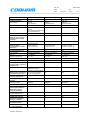
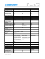
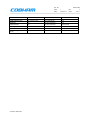
Doc. No.:
GR740-CMP
Issue:
1
Rev.:
Date:
2015-03-17
Page:
COMPARISON BETWEEN
GR740, LEON4-N2X AND NGMP
© Aeroflex Gaisler AB
3
1 of 11
Doc. No.:
GR740-CMP
Issue:
1
Rev.:
Date:
2015-03-17
Page:
4
2 of 11
TABLE OF CONTENTS
1 INTRODUCTION............................................................................................................................ 3
1.1 Scope of the Document........................................................................................................ 3
1.2 Reference Documents.......................................................................................................... 3
2 COMPARISON BETWEEN GR740, LEON4-N2X AND NGMP...................................................... 4
2.1 Overview............................................................................................................................... 4
2.2 Comparison.......................................................................................................................... 5
2.3 Changes in memory map................................................................................................... 10
© Cobham Gaisler AB
Doc. No.:
1
GR740-CMP
Issue:
1
Rev.:
Date:
2015-03-17
Page:
4
3 of 11
INTRODUCTION
1.1 Scope of the Document
This document lists the diferences between the Cobham Gaisler GR740 device and
prototypes that have preceded this device. The document also compares the GR740 with
other radiation-hard LEON devices.
This document supersedes the document Diferences Between NGMP Functional Prototype
and Baseline NGMP Design, NGFP-FPDIFF-0016.
Note that this document describes an ongoing development. Performance and timing
parameters of the GR740 device may change once devices have passed manufacturing,
testing and characterisation.
1.2 Reference Documents
[NGMP] “Quad Core LEON4 SPARC V8 Processor, Data Sheet and User's Manual”, Aeroflex
Gaisler, LEON4-NGMP-DRAFT-2-2, May 2013
[LEON4-N2X] “Quad Core LEON4 SPARC V8 Processor, LEON4-N2X, Data Sheet and User's
Manual”, Aeroflex Gaisler, LEON4-N2X-DS-2-9, October 2014
[GR740] “Quad Core LEON4 SPARC V8 Processor, GR740, Data Sheet and User's Manual”,
Cobham Gaisler, LEON4-GR740-UM-DS-D1, March 2015
[MMUTN] “Technical Note on LEON SRMMU Behaviour”, Cobham Gaisler, TN-LEON-SRMMU,
January 2015
© Cobham Gaisler AB
Doc. No.:
2
GR740-CMP
Issue:
1
Rev.:
Date:
2015-03-17
Page:
4
4 of 11
COMPARISON BETWEEN GR740, LEON4-N2X AND NGMP
2.1 Overview
The GR740 device is a result of the work performed within the Next Generation
Microprocessor (NGMP) activity initiated by ESA/ESTEC. Within this activity there, have been
several NGMP FPGA prototypes developed and a functional prototype, LEON4-N2X, was also
developed.
The block diagram below shows the architecture of the GR740 device. The table in in
section 2.2 lists diferences between the GR740 [GR740], LEON4-N2X [LEON4-N2X] and
NGMP baseline design [NGMP]. Please note that the design described by [NGMP] has
undergone changes throughout the development. This document describes the diferences
between designs for the latest data sheets at the time of writing. FPGA prototypes of the
NGMP design are reduced versions of the NGMP design and have additional diferences.
The comparison is intended to be useful for users without prior knowledge of the NGMP
project, where the information in this document can be used to assess if the LEON4-N2X is
a suitable prototype for specific GR740 applications.
Figure 1: GR740 block diagram
© Cobham Gaisler AB
Doc. No.:
GR740-CMP
Issue:
1
Rev.:
Date:
2015-03-17
Page:
4
5 of 11
2.2 Comparison
The table below compares [GR740], [LEON4-N2X] and [NGMP]. Rows with diferences have
bold text in the Feature column.
Feature
GR740
LEON4-N2X
NGMP
Technology
STM C65SPACE
eASIC Nextreme2
STM Space DSM (target)
Device ID / Build ID
0x740 / 4152
0x280 / 4114
0x280, 0x281 / -
Radiation-tolerant
Yes
No
Yes
Package
LGA625 (CCGA w. columns)
FC896
Ceramic flip-chip target
CPU
4 x LEON4
4 x LEON4
4 x LEON4
Protection of register files and (No protection of L1 cache Protection of register files and
L1 cache
and register files)
L1 cache
FPU
4 x GRFPU
(one per CPU)
CPU,FPU clock
250 MHz
150-200 MHz
(TBC, estimated worst case at
125°C and 20 years lifetime)
400 MHz target
Level-1 (L1) cache
I: 4x4KiB, D: 4x4KiB
I: 4x4KiB, D: 4x4KiB
L1 cache replacement
policy
Soft
configurable:
Least- Least-Recently-Used
Recently-Used,
Random,
Direct-mapped
L1 cache physical (snoop) Yes
tag error counter
Branch prediction
2 x GRFPU
(shared per CPU pair)
I: 4x4KiB, D: 4x4KiB
No
Yes, can be disabled via Yes
%ASR17
4 x GRFPU
(one per CPU)
Soft configurable
No
Yes
Disable branch prediction Yes, can be controlled via No
on i-cache miss
%ASR17
No
LEON4 time-stamp counter Yes
(%ASR22/23)
No
No
LEON4 support for SPARC Yes
V8E
nonprivileged
ASI
access
No
No
LEON4 HW watchpoints Yes
trigger on least significant
word of LDD/STD
No
No
Memory Management Unit
Yes. Fault Status register and Yes
Fault Address Register update
conditions have been changed
compared to earlier versions.
See [MMUTN].
Yes
Shared Level-2 cache
Yes
Yes
Yes
Level-2 cache size
4 x 512 KiB
2048 KiB total
4 x 64 KiB
256 KiB total
4 x 128 KiB
512 KiB total
L2-cache EDAC
Yes
No (sim. timing)
Yes
L2-cache scrubber
Yes
No
Yes
Pipeline stage between
LEON4 and L2 cache
Yes, increases latency of read
and write accesses on
Processor AHB bus.
No
No
L2-cache support for
serving cache hits during
miss processing
Yes, via the use of SPLIT No
transactions
No
© Cobham Gaisler AB
Doc. No.:
Feature
GR740
GR740-CMP
Issue:
1
Rev.:
Date:
2015-03-17
Page:
LEON4-N2X
4
6 of 11
NGMP
On-chip buses
5xAHB, 2xAPB
5xAHB, 2xAPB
5xAHB, 2xAPB
On-chip bus frequency
Same as CPU
Same as CPU
Same as CPU
CPU bus
128-bit AHB
128-bit AHB
128-bit AHB
Memory bus
128-bit AHB
128-bit AHB
128-bit AHB
I/O Master bus
32-bit AHB
32-bit AHB
32-bit AHB
I/O Master access control
GRIOMMU
GRIOMMU
GRIOMMU
I/O master bus SPLIT
support
No
Yes, configurable by software.
Yes, configurable by software.
IOMMU bus selection
Via registers and IOPTE
Not supported
Via registers
IOMMU number of groups
8
8
6
I/O Slave bus
32-bit AHB
32-bit AHB
32-bit AHB
APB bus connected to CPU
bus
Yes
No (connected to slave I/O No (connected to slave I/O
bus)
bus)
Debug bus
32-bit AHB
32-bit AHB
32-bit AHB
Debug bus clock gating
Yes (via DSUEN)
Yes (via DSUEN)
Yes (via DSUEN)
Main memory controller
SDRAM
Multiplexed DDR2/SDRAM
w. separate pins
Multiplexed DDR2/SDRAM
Memory width
64+32 / 32+16
64+32 / 32+16
64+32 / 32+16
Memory speed
Up to 100 MHz SDRAM (PCB 300 MHz DDR2,
timing limited)
100 MHz SDRAM
400 MHz DDR2,
133 MHz SDRAM
SDRAM 2T signalling
Yes
No
No
Memory EDAC
4x-interleaved RS
4x-interleaved RS
4x-interleaved RS
Widest SEU tolerance
16-bit lane
16-bit lane
16-bit lane
Memory failover
Yes
Yes
Yes
External memory scrubbing in
hardware
Yes
Yes
Yes
PROM controller
FTMCTRL 8/16-bit
FTMCTRL 8/16-bit
FTMCTRL, 8/16-bit
PROM EDAC
Yes, in 8-bit mode
Yes, in 8-bit mode
Yes, in 8-bit mode
PROM lead-out cycles
Configurable by SW
2
4
SpaceWire
GRSPWROUTER
8 SpW ports
4 AMBA ports
GRSPWROUTER
8 SpW ports
4 AMBA ports
GRSPWROUTER
8 SpW ports
4 AMBA ports
SpaceWire-D support
Hardware support
No hardware support
No hardware support
SpaceWire-PnP support
Yes, subset
No
No
SpaceWire distributed
interrupt support
Yes, 32 interrupts with
No
acknowledgements and 64
interrupts, selected via
bootstrap signals and software
configurable.
No
SpaceWire Time-Code
filtering
Connected to TDP controller Needs to be implemented in Needs to be implemented in
and support for Time-Code software.
software
filtering in SpaceWire router
AMBA ports.
SpaceWire clock
300 MHz
200 MHz
200 MHz
SpaceWire sampling
DDR
DDR
DDR
SpaceWire buffers
Protected RAM
Unprotected RAM
Protected RAM
MIL-STD-1553B
GR1553B 1xdual-red.
GR1553B 1xdual-red.
GR1553B 1xdual-red.
© Cobham Gaisler AB
Doc. No.:
Feature
GR740
GR740-CMP
Issue:
1
Rev.:
Date:
2015-03-17
Page:
LEON4-N2X
NGMP
CAN 2.0B controller
Yes, two
No
Yes, one
PCI interface
GRPCI2
32-bit TBD MHz
GRPCI2
32-bit 33/66 MHz
GRPCI2
32-bit 33/66 MHz
PCI Arbiter on-chip
No
Yes
Yes
PCI buffers
Implemented with rad-hard Unprotected
flip-flops.
Trace buffer with implemented
with unprotected RAM.
Protected
Ethernet
2 x GRETH_GBIT
2 x GRETH_GBIT
2 x GRETH_GBIT
Ethernet controller RAM
debug access (access to
internal buffers via APB
interface)
Disabled
Yes
Yes
Ethernet buffers
Protected RAM
(except EDCL data)
Unprotected RAM
Protected RAM
Ethernet Debug
communication Link MAC
Addresses
00:50:C2:75:A3:30
00:50:C2:75:A3:40
00:50:C2:75:A0:60
00:50:C2:75:A0:70
00:50:C2:75:A0:60 - 7F
00:50:C2:75:A3:00 - 3F
High-Speed Serial Links
No
No
Yes
SPI Controller
SPICTRL master/slave
SPICTRL master/slave
SPICTRL master/slave
UART:s
2 x APBUART
2 x APBUART
2 x APBUART
General-purpose timer
1x5 + 4x4
1x5 + 4x4
1x5 + 4x4
Timer latch capability
Yes
No
No
Watchdog output
Yes
Yes
Yes
Watchdog clocked directly
by input clock to catch PLL
related events
Yes
No
No
GPIO
16 + 22 shared on pins
(additional GPIO port
peripheral included in design)
16
16
GPIO toggling controlled by
internal hardware events
Yes. Timer ticks and latch
events can toggle GPIO.
No
No
GPIO interrupt available and Yes
interrupt flag registers
No
No
GPIO logical-or,-and-xor
registers
Yes
No
No
Interrupt controller
IRQ(A)MP
IRQ(A)MP
IRQ(A)MP
Interrupt (re)map support
Yes
No
No
Timer value synchronized
between DSU, AHB trace
buffer and interrupt
controller timestamp
Yes
No
No
Performance counters
(L4STAT statistics unit)
Yes
Yes
Yes
CCSDS TDP controller
Yes
No
No
Number of performance
counters in L4STAT
16
4
4
Performance counter events Yes
from Master I/O bus
No
No
Performance counter events Yes
for AHB REQ/GRANT
No
No
© Cobham Gaisler AB
4
7 of 11
Doc. No.:
Feature
GR740
GR740-CMP
Issue:
1
Rev.:
Date:
2015-03-17
Page:
4
8 of 11
LEON4-N2X
NGMP
Performance counter events Yes (for hit, miss, access)
per master from L2 cache
No (combined for all masters)
No (combined for all masters)
Performance counter events Yes
for L2 cache EDAC
No
No
Performance counter
latching and timestamp
Yes
No
No
Master I/O trace buffer
filters for RETRY response
Yes
No
No
Spacewire debug link
Yes, separate GRSPW2
Yes, separate GRSPW2
Yes, separate GRSPW2
USB debug link
No
Yes
Yes
JTAG debug link
Yes
Yes
Yes
Ethernet debug link
Yes (2x)
Yes (2x)
Yes (2x)
Ethernet debug link can be
disabled via separate
bootstrap
Yes
No
No
DSU AHB trace buffer size
4 KiB
4 KiB
4 KiB
Instruction trace buffer size
8 KiB
4 KiB
4 KiB
Instruction trace buffer can
be written via DSU register
i/f.
Yes
No (not all lines)
Yes
Instruction trace buffer can
be read while processor is
executing
Yes
No
No
Instruction trace buffer
overflow detection
Yes
No
No
DSU trace buffers enabled
after reset
Yes, when DSUEN='1' and No
BREAK='0'.
No
Debug units clock gated by
DSUEN
Yes
Yes
Yes
Reset and clocking scheme
Single reset input is
connected to all internal
interfaces and clock domains
(including PCI, Ethernet, MILSTD-1553B and SpaceWire)
reset lines.
Multiple reset inputs for
different interfaces.
Multiple reset inputs for
different interfaces.
Clocking scheme differs from
NGMP specification. See user
manual and data sheet for
details.
Clocking scheme differs from
NGMP specification. See user
manual and data sheet for
details.
Clock gating unit
Yes, extended to allow manual Yes
gating of additional
peripherals
Yes
FPU clock gating controlled
separately from CPU clock
Yes
Yes (for shared FPU)
No
Dynamic PLL control
Yes
Yes
Not specified
Dynamic Pad control
Yes
Yes
Not specified
Pin multiplexing
Yes
No
Yes (between DDR2 SDRAM
and SDRAM)
Temperature sensor
Yes
No
No
General purpose register for Yes
bootstrap signals
No
No
© Cobham Gaisler AB
Doc. No.:
Feature
GR740
GR740-CMP
Issue:
1
Rev.:
Date:
2015-03-17
Page:
LEON4-N2X
NGMP
JTAG boundary scan
Yes, using SoC TAP
Yes, separate TAP
Yes
Scan test
Yes
Not user-accessible
Yes
OCC scan test
Yes
Not user-accessible
Not specified
Memory BIST
Yes, accessed via JTAG
Not user-accessible
Not specified
Clock-to-out test modes
SDRAM, PCI, ETH
No
Not specified
[LEON4-N2X], section 44,
errata
Not affected
Affected
-
© Cobham Gaisler AB
4
9 of 11
Doc. No.:
GR740-CMP
Issue:
1
Rev.:
Date:
2015-03-17
Page:
4
10 of 11
2.3 Changes in memory map
Some cores do not exist in all designs and are missing in the memory map. Peripherals that
have been moved are:
•
L4STAT: Debug bus base address for the L4STAT unit has been changed in GR740
compared to LEON4-N2X/NGMP.
•
GR1553B: Base address for the MIL-STD-1553B controller has been changed in
GR740 compared to LEON4-N2X.
•
PCI arbiter is not included in the design. CAN controller APB interface moved to PCI
arbiters position on APB bus when compared to LEON4-N2X/NGMP.
•
General purpose register bank: Address map has been changed between LEON4-N2X
and GR740. Peripheral is not included in NGMP specification. The functionality driven
by the registers are diferent between the devices.
© Cobham Gaisler AB
Doc. No.:
GR740-CMP
Issue:
1
Rev.:
Date:
2015-03-17
Page:
4
11 of 11
Copyright © 2015 Cobham Gaisler
Information furnished by Cobham Gaisler is believed to be accurate and reliable. However,
no responsibility is assumed by Cobham Gaisler for its use, or for any infringements of
patents or other rights of third parties which may result from its use. No license is granted
by implication or otherwise under any patent or patent rights of Cobham Gaisler.
All information is provided as is. There is no warranty that it is correct or suitable for any
purpose, neither implicit nor explicit.
© Cobham Gaisler AB