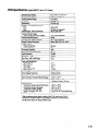
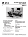
1
The 5B Series
User’s Manual
Copyright0 1987
AnalogDevicesInc.
OneTechnologyWay
P.O.Box 9106
Norwoo$,Massachusetts0206?-9106
All rights reserved.No part of this publicationmay be reproduced,storedin a
retrievalsystemor transmittedin any form by any means,electkmic,mechanical photocopying,recoding,or otheiwise,without theprior writdenpermission
of Analog DevicesInc.
Printedin U.S.A.
Part# 98-1323301
RevisionRecod
Publication# G 1114~20-8/87
Revision1.O,Released8/87
Revision2.0,ReleasedY88
Revision3.0,Released2/90
.
Table of Contents
Chapter 1 - Introduction
GeneralDescription..................................................................................................
l-l
Applications ............................................................................................................
l-l
5B SeriesModules ...................................................................................................
1-2
Chapter 2 - Module Specifications
Features....................................................................................................................
2-1
Module Description.......................................................................
...........................
2-l
Performance.............................................................................................................
2-1
Evaluationand Test...........................................................................................
2-1
Protection...........................................................................................................
2-1
PhysicalCharacteristics....................................................................................
2-1
Modules....................................................................................................................
2-3
5B30 and 5B31 Millivolt and Voltage Input Modules .....................................
2-4
5B32 CurrentInput Module ..............................................................................
2-6
5B34 RTD Input Module ..................................................................................
2-8
5B37 ThermocoupleInput Module .................................................................
2-10
5B38 Strain GageInput Module .....................................................................
2-12
5B39 CurrentOutput Module .........................................................................
2-14
5B40 and 5B41 Wide BandwidthMillivolt andVoltage Input Modules .......2-16
5B45 and 5B46 FrequencyInput Modules ....................................................
2-18
5B47 LinearizedThermocoupleInput Module ...............................................
2-20
AC1367 Switch Input Module ........................................................................
2-22
Chapter 3 - 5B Series Subsystem Solutions
5BOl Backplane.......................................................................................................
3-1
ConnectorPin Usage.........................................................................................
3-1
Grounding .........................................................................................................
3-3
Fusing andPolarity Reversal............................................................................
3-3
InterchannelBridge Jumpers............................................................................
3-3
5BO2Backplane....................................................................................................... 3-3
ConnectorPin Usage.........................................................................................
3-4
Grounding .........................................................................................................
3-4
AddressSelectionJumpers...............................................................................
3-6
Fusing andPolarity Reversal............. ............................................................... 3-6
5BOl and 5B02 BackplaneSpecifications...............................................................
3-6
5B03 and 5BO4Backplanes......................................................................................
3-7
5BO3and 5BO4BackplaneSpecifications...............................................................
3-7
Power Requirements................................................................................................ 3-8
Field Terminations...................................................................................................
3-9
Installation ..............................................................................................................
3-10
InterfaceAccessories..............................................................................................
3-11
Chapter 4 - System Design Considerations
PhysicalDesignIssues............................................................................................. 4- 1
ProcessSideIssues................................................................................................... 4-3
Field Terminations............................................................................................ 4-3
AC1361 Cold JunctionTemperatureSensor................‘...................................
4-3
Current ConversionResistor............................................................................. 4-4
Protection.......................................................................................................... 4-4
Safety ............................................................................................................ 4-4
Isolation ............................................................................................................ 4-4
10/l/95
iii
Table of Contents (cont.)
4-5
SystemSide Issues..................................................................................................
4-5
Grounding................................................................................................................
4-5
Using the Input Modules’Output Switch ................................................................
4-5
Effects of the Output Switch ...................................................................................
4-5
Using the Output Modules’Track-and-Hold...........................................................
4-5
MiscellaneousTopics ..............................................................................................
4-5
AC1360 EvaluationSocket.....................................................................................
........................................................................
.4-6
Two Levels of Isolation protection
4-6
Use with Two Wire Transmitters............................................................................
A-l
Appendix A - Accessories..............................................................................................
B-l
Appendix B - Drill Template..........................................................................................
C-l
...................................................................
Appendix C - 5B02 JumperConfigurations
D-l
Appendix D - 5B37 TransferFunction...........................................................................
IV
List of Figures
Figure
1.1
2.1
2.2
2.3
2.4
2.5
2.6
2.7
2.8
2.9
2.10
2.11
3.1
3.2
3.3
3.4
3.5
3.6
3.7
3.8
3.9
3.10
3.11
3.12
3.13
3.14
3.15
4.1
4.2
4.3
4.4
4.5
4.6
4.7
4.8
4.9
4.10
Description
Page
FunctionalBlock Diagramof a GeneralMeasurementat&Control
l-l
Application Using the 5B Series........................................................................
2-2
5B SeriesModule Outline andPin Designations..................................................
2-4
5B30 and 5B31 FunctionalBlock Diagram ..........................................................
5B32 FunctionalBlock Diagram...........................................................................
2-6
2-8
5B34 FunctionalBlock Diagram...........................................................................
2-10
5B37 FunctionalBlock Diagram.........................................................................
2-12
5B38 FunctionalBlock Diagram.........................................................................
2-14
5B39 FunctionalBlock Diagram.........................................................................
2-16
5B40 and 5B41 FunctionalBlock Diagram ........................................................
2-18
.................................
5B45 and 5B46 FunctionalBlock Diagram .......................
5B47 FunctionalBlock Diagram.................................................................
..- .... 2-20
2-22
AC 1367.FunctionalBlock Diagram....................................................................
3-l
5BOl Diagram .......................................................................................................
5BOl Schematic.....................................................................................................
3-2
5BOl SystemConnectorPinout.............................................................................
3-3
5BO2Diagram .......................................................................................................
3-4
3-5
5BO2SystemConnectorPinout.............................................................................
3-4
5BO2Schematic.....................................................................................................
3-6
AddressSelectionPins - Default Jumpers.............................................................
5B03 Wiring Diagram ...........................................................................................
3-7
5BO4Wiring Diagram ...........................................................................................
3-7
3-8
Power Connection.................................................................................................
3-9
.;........................................
Input Field Connections..............................................
3-9
5BOl and 5B02 BackplaneMounting Dimensions...............................................
3-9
AC 1363Rack Mount Diagram..............................................................................
3-10
Rack Mount AssemblyDrawing .........................................................................
3-10
AC1324 Diagram.................................................................................................
4-2
5B SeriesModule Outline andPin Designations..................................................
4- 1
5BOl BackplaneChannel......................................................................................
4-3
AC1361 Connection..............................................................................................
4-3
AC1361 Outline.....................................................................................................
4-4
AC1361 Test Circuit ..............................................................................................
4-4
AC 1362Outline.....................................................................................................
4-5
AC1360..................................................................................................................
4-6
Double IsolationProtection...................................................................................
4-7
CurrentLoop Input from Loop-PoweredTransmitter(2-Wire) ............................
CurrentLoop Input from Locally-PoweredSource(or 3/4 wire Transmitter)...... 4-7
List of Tables
Table
1.1
2.1
3.1
3.2
4.1
10/l/95
Description
Page
l-2
Available 5B SeriesModules ................................................................................
2-3
5B SeriesInput Modules .......................................................................................
3-6
AddressSelectionJumpers....................................................................................
3-8
Module PowerRequirements................................................................................
4-3
AC1361 Electrical Specifications..........................................................................
V
June, 98
iI5B Series
New Product Inforrbation
Data Sheets for the following New
5B Series1products are attached:
5l)O8/5BOS-MUX
S-ahanne Backplanes
5B35
4-WifeI RTD input modMe
5B36
PotentiomQterIResistor input module
.5B42
4-to-20 mA PirocessCurrent input module
Visit our new ANALOG DEiVICES 10s Website @ htW/www.analoa.com
for...
l
The Latest Data Sheets ~
l
Technical Support (i&ldding answers to Frequently Asked Questions)
l
Alternate Source Produdt Cross Reference
l
Sales Offices - Addresse$PhonelFax
l
New 3-Year Warranty Statement
l
and More!!!
ANALOG
DEVICES
I
5BSeries
8$hannelBackplanes
! 5B08/5B08=MUX
FEATURES
8Channel. Industry Standard 5B Series Compatibility
Two Backplane Selections
5B08: Eight :lndependent I/O Channels
5B08MUX: Eight I/O Channels Multiplexed onto One Bus
Mix and Match 5B Series I/O Module Capability
Thermocouple,
RTD, mV, V, Frequency, mA, Strain
Gage, Loop-Powered
mA, Potentiometer,
Slidewire
-25°C to +85”C Temperature Range
1500 V rms WanKhan
and Input/Output
Isolation
FM Approved
Approved for Use in Class I, Division 2, Groups A, B,
C and D Locations
CE Appioved
EMC Directive In Heavy Industrial Applications
APPLICATIONS
Front-End Data Acquisition Systems
Process Control and Monitoring
Product Test
GENERAL
DESCRIPTION
Pl/P2
The 5B08 and 5BWMUX backplanesaccept up to eight 5B
Seriesinput/output modules, providing direct screw terminal
interfacing to sensorsand transducers, as well as a 26-pin
connector I/O interface to a measurementand control system
(refer to Figures 2 :and 3 for functional block diagrams). Model
5B08 backplane I/O signals are independently available, while
Model 5B08-MUX I/O signals are controlled via an on-board
multiplexer providing a bus for input signalsand a separatebus
for output signals. 5B Seriesmodules can be mixed or matched
and may be changed without disturbing field wiring. Each
channel has a coldIjunction temperaturesensor(Model AC1361)
to accommodatethermocouple modules (5B37 or 5B47). Both
backplanesrequire an external +5 V dc regulated power supply.
Reversepower supply protection is provided aswell asa replaceable 4-amperefuse!anda power ON greenLED indicator.
5B08 SYSTBM
CONNECTORS
Signal connections between the 5B08 and the associated
measurementand control system are made with two identical
26-pin connectors (Pl and P2), similar to the 16-channel model
5BOl backplane. Referenceto these connectors is electrically
identical and may Ibeuseful if a 5B08 is used for both analog
input and analog output and the data acquisition systemhas
separateinput or output connectors. Figure 1 illustrates the pin
assignmentsfor PI and P2.
CHO
1
0
0
2
CHB
cou
3
0
0
4
CH9
CHl
5
0
0
6
COP
CH2
7
0
0
8
CHlO
COM
9
0
0
10
CHll
CH3
11
0
0
12
COM
CH4
13
0
0
14
CH12
COM 15
0
0
16
CH13
CHS
17
0
0
18
corn
CH6
19
0
0
20
CH14
COM 21
0
0
22
CH16
CH7
23
0
0
24
COM
SENSE
25
0
0
126
NC
TOP VIEW
Figure
7. S&8
System
Connector
Pinout
REV. A
Information furnished by Analog Devices is believed to be accurate and
reliable. However, no responsibility is assumed by Analog Devices.for its
use, nor for any infringements of patents or other rights of third parties
which may result from its use. No license is granted by implication or
otherwise under any patent or patent rights of Analog Devices.
One Technology Way, P.O. Box 9106, Norwood, MA02062-9106, U.S.A.
Tel: 781132%4700
Wbrld Wide Web Site: http://www.analog.com
Fax: 7811326-8703
0 Analog Devices, Inc., 1998
5B08/5B08-MUX-SPECIFICATIONS
(typicalQ +25”Cand+5 V deunlessothetwisenoted)
Model
5B08
5B08-MUX
3.5" x 10.0" x 3.2"
(88.9 mm x 254.0 mm x 8 1.3 mm)
*
7 02 (200 g)
*
5
*
COLD JUICTION TEMPERATURE SENSORS
(Provided On Backplane)
Accuracy @ +2YC
Over t5”C to t45”C
8, Model AC 1361
f0.25'C (kO.75'C max)
+0.5"C (iO.O125"C/"C)
*
*
*
SYSTEM CONNECTOR
26-Pin Male Mating
Amp 746290-6
*
ADDRESS SELECTION INPUTS
Max Logic “0”
Min Logic “ 1”
Max Logic “1”
N/A
N/A
N/A
to.8 V
t2.0 v
CHANNELS
DIMENSION-WITH
5B SERIES MODULES
WEIGHT
MOUNTING
STANDOFFS
POWER SUPPLY
Voltage: Operating
Voltage: Max Safe Limit-With
Current-Without Modules
Fuse (Fl)
+7.0 v
*
*
+5Vdc+ 5%
t6.0 V dc max
13mA
4 Ampere
Littelfusee Type 252 004
Modules
TEMPERATURE RANGE
Rated Performance
Storage
Relative Humidity
*
40 mA
*
-25°C to +85”C
-40°C to +85’C
0 to 95% @ +60°C Noncondensing
*
*
*
*Specifications sameas Model 5B08.
Specitications subject to changewithout notice.
ADDRESS
OEOODERS
--
-EL
0
CMNNEL
1
Figure 2. 5808 Functional
CIIANNEL
7
CHANNEL
s
CIUMJEI.
0
Figure 3. 5B08-MUX
Block Diagram
CIWWEL
1
Functional
CHINNEL
I
ClUN4EL
s
Block Diagram
All trademarks are the property of their respective holders.
-2-
REV. A
The I/O connectors provide a signal path for each channel and,
in addition, a number of grounding pins are available to provide
interchannel shield conductorsin the ribbon cable. In somecases,
discussedbelow, the ground conductors will not provide an
accuratesignal reference,so a SENSE pin is also provided in the
connectors. Several jumper and component options on the 5BO8
provide optimum ground connections for various applications.
Table II shows the chsnnel assignments when Jumpers Jl-J7 .r
are used. Additional configuration flexibility is provided when
the output jumper selections (J8-Jl5) are combined with the
inter-channel jumper:selections(Jl-J7). Table III provides the
resulting signal assignmentsfor each of the various jumper
selections.
Table II. 5B08 Interchannel
SBOSOUTPUT
CHANNEL
To configure Model 5B08 I/O for different system needs, onboard jumpers are provided. A family of eight 3-pin jumpers,
J8 through J15, allows the user to assign the 5B08 I/O to either
the upper eight L/O pins (CHO, CHI, CH2, CH3, CH4, CH5,
CH6, CH7) or to the lower eight I/O pins (CH8, CH9, CHlO,
CH11, CH12, CHl3, CHl4, CHl5). This capability allows
two 8-channel 5B08 backplanes to be used in a 16-channel
configuration, with all I/O assignedto the 16 unique I/O pins,
CHO-CHIS. Table I illustrates the channel assignmentsfor
each of the eight jumpers, J8 through Jl5.
Jl
Channel 0 Vou~ to
Channel 1 Vow to
Channel 2 Vow to
Channel 3 Vow to
Channel 4 Vow to
Channel 5 Vom to
Channel 6 V0t.n to
-3-
Channel 1 V,
Channel 2 Vn,
Channel 3 VG
Channel 4 VI,
Channel 5 V,
Channel 6 VW
Channel 7 V,
Using Output and
Jumper
Closed
Ou$ut (a
Jumper SF
J1
J8 LO
J8 HI
JS LO
J8 HI
J9 LO
J9 LO
J9 HI
J9 HI
Channel 0
to
Channel 1
J2
J9 LO
J9 HI
J9 LO
J9 HI
JlO LO
JlOLO
JlO HI
JlO HI
1 to 2
Channel 1
9 to 2
to
Channel 2% 1 to 10
9to 10
.J3
JlO LO
JlO HI
JlO LO
JlO HI
Jll
Jll
Jll
Jll
LO
LO
HI
HI
Channel 2
to
Channel 3
2 to 3
lOto
2to 11
lOto 11
J4
Jll
Jll
Jll
Jll
LO
HI
LO
HI
J12 LO
J12 LO
J12 HI
J12 HI
Channel 3
to
Channel 4
3 to 4
11 to4
3 to 12
11 to 12
J5
J12 LO
J12 HI
J12 LO
J12 HI
J13 LO
J13LO
J13 HI
i Jl3HI
Channel 4
to
Channel 5
4 to 5
12to5
4to 13
12 to 13
J6
J13 HI
J13 LO
J13 HI
J13 LO
Channel 5
to
Channel 6
5 to 6
13to 6
5to 14
13 to 14
J7
J14 HI
J14 LO
J14 HI
J14 LO -
JUMPERS
The 5B08 offers ithe user the ability to easily connect the voltage
output of any 5B Series input module directly to the voltage
input of an adjacent output module (e.g., Model 5B39) by
placing a jumper over two pins (Jl, J2, J3, J4, J5, J6 or J7). This
feature can be used to provide an isolated current output
from an isolated input module. This results in both isolated
voltage and isolated current outputs from a single sensor
input signal. A kit of ten jumpers is available as Model AC1344.
REV. A
~conuects
Table III. 5B08 C mnel Assignments
Interchannel Jum PC!lS
15
HI
jumper
J2
Table I. SBOSOutput Channel Assignments
SBOSINTERCHANNEL
Jumpers
SELECTION
Connects
V/I Channels
Connects
J14 LO
J14LO
J14 HI
J14HI 1
I
J15 LO
J15 LO
JIS HI
J15 HI
0 to 1
8 to 1
0 to 9
8 to 9
1
Channel 6
to
Channel 7
6 to 7
14to 7
6to 15
14 to 15
5B08 GROUND JUMPERS
Pl
Model 5B08 is supplied with three grounding jumpers: WI, W3
and W4. These three jumpers are installed at the factory, but can
be changedto accommodateuser system configuration needs.
Jumper Wl connects the El and P2 shield pins (Pins 3, 6, 9, 12,
15, 18,2 1 and 24) to the 5B08 I/O common (backplanemeasurement ground). This will usually be the primary ground connection.between the 5B08 backplane and the measurementsystem.
This connection is required ifoutput modules are used on the 5BO8. It
is also required if there is no high impedance senseinput (input
LO of a differential or pseudo-differential system) availableon
the measurement system.
Jumper W3 connects the senseinput, if available on Pin 25, to
the 5B08 I/O common, so it can be read directly. W3 can be left
in place at all times.
Jumper W4 connects the 5B08 I/O common to the +5 V power
common. A connection between power common and I/O
common is important for the 5B Series modules to function
properly; however, if this connection is made elsewherein your
system (the best place is usually near the A/D or D/A converters),‘W4 should be cut since a ground loop could result.
hEAD
UOCOY
l-
0
2
UOCOM
0
0
4
SNSLO
0
0
6
UOCOM
BIT2
1
LSB
7
0
0
BIT3
9
0
0
10
BIT4
BITS
11
0
0
12
MSB
LSB
13
0
0
BIT3
15
0
0
16
BIT4
BITS
17
0
0
18
14
MS6
Brr2
READ WB (0)
19
0
0
20
WRmE ENB (0)
NC
21
0
0
22
RESERVW
NC
23
0
0
24
NC
25
0
0
26
DCOM
READ
(INPUT)
ADDRESS
1
WRITE
(OuTPllT)
ADDRESS
DCOM
1
TOP VIEW
VRUD IS THE ANALOG
INFORMATION
IS THE ANALOG
OUTPUT OF INPUT MODULES
INPUT OF OUTPUT MODULES
NC i NO CONNECT
See the “5B08/5B08-MUX” sections of this data sheetfor
additional information on Model 5B08.
Figure 4. 5B08-MUX
System
Connector
Pinout
SBOS-MUX GROUND JUMPERS
SBOS-MUX DESCRIPTION
Model 5B08-MUX is supplied with three grounding jumpers:
W 1, W2 and W4. These three jumpers are installed at the
factory, but can be changed to accommodate user system
configuration needs.
The 5B08-MUX incorporates input and output busesthat take
advantageof the internal series output switches in the 5B Series
input modules as well as the track-and-hold circuit in the output
modules. Designers integrating the 5BO8-MUX into a measurement and control system do not need external multiplexers and
can use a single digital-to-analog converter to servenumerous
output channels;‘Referto Figure 3 for a functional block diagram
and Figure 6 for a schematic diagram of model 5B08-1\IUX.
Digital outputs from the host data acquisition system are used
to addressthe 5B Seriesmodules and designateinputs and
outputs. Only one analoginput, one analog output and a number
of digital outputs are required to address up to 64 analog input/
output channels using eight 5B08-MUX backplanes.
MODEL
5
0
8
Vwm
5B08 ADDITIONAL
1
Jumper Wl connects the El shield pins (Pins 2, 5 and 6) to the
5B08-MUX backplane common (backplane measurement
ground). This will usually be the.primary ground connection
between the 5B08-MUX backplane and the measurement
system. This wnnection is required ifoutput modules are used on the
5BO8-MUX. It is also required if there is no high impedance
senseinput (input LO of a differential or pseudo-differential
system) available on the measurement system.
Jumper W2 connects the senseinput from the measurement
system, if available on Pin 4, to the 5B08-MUX backplane
common, so it can be read directly. W2 can be left in place
at all times.
SBOS-MUX SYSTEM CONNECTOR
Signal connections between’the 5B08-MUX and the associated
measurement or control system are made at PI, a 26-pin
connector. The pinout of Pl is shown in Figure 4.
Jumper W4 connects the 5BQ8-MUX backplane common to the
+5 V power common. A connection between power common
and I/O common is important for the 5B Series modules to
function properly; however, if this connection is made elsewhere
in your system (the best place is usually near the AID or D/A
converters), W4 should be cut since a ground loop could result.
One signal path is provided for inputs and one for outputs.
Input and output modules are independently addressedby two
sets of six addresspins and an enable pin. In addition, a number
of grounded pins are present in the connector pinout to provide
shield conductors in the ribbon cable. In some cases,discussed
below, the ground conductors will not provide an accurate
signal reference, so a SENSE pin (SNS LO) is also provided in
the pinout. Several jumper and component options in the
backplane provide optimum ground connections for various
circumstances.
-4-
REV. A
5BO8/5BOS=MUX
SBOS-MUX ADDRESS
JUMPERS
SBOSISBOS-MUX GROUND
5B08-MUX backplane can hold eight 5B Seriesmodules in any
combination of inputs or outputs. Address decoderson the
backplane determine which module is read (input type) or
driven (output type). Separate decoders are provided for
inputs and outputs. To permit system expansion, up to eight
5B08-MUX backplanes can be daisy-chained on the system
I/O ribbon cable for a total of 64 channels.Jumpers on each
backplane (labeled Jl-J9 and JIO-JlS) determine the block of
eight addressesassignedto each backplane. Input (read) and
output (write) addressing are completely independent; in all
cases,JumpersJl-J9 control inputs and JIO-Jl8 control
outputs. Independent addressing might be used, for example, to
update output modules without interrupting the monitoring of
input modules.
Table IV. SBOS-MUX Address Jumpers
Input
Jumper
output
Jumper
Address
Raw9
g
J12
J11
48-55
56-63
;
:;
J13
J14
J15
J16
4047
32-39
24-3
16-231
J8
J9
J17
J18
8-15
SBOS-MUX FACTORY
JUMPER
o-7
SETTINGS
5B08-MUX backplanes are factory configured with jumpers at
positions Jl and JlO. This sets up the 5B08-MUX backplane as
a stand-alone 8-channel system. Moving the jumpers to any
other position in!the two blocks of jumpers enablesdecoding of
the full six addreksbits; the exact position of the jumper
determines addressposition for the 5B08-MUX backplane as
shown in Table IV. To use multiple SBOS-MUX backplanesin
this manner, connect the corresponding I/O connector pins of
each backplane in parallel. Model CAB-01 cable is a ribbon
cable with three 26-pin connectors designedfor this purpose.
SBOS/SB08-MUX FUSING AND POLARITY
REVERSAL
Since reversing the polarity of the t5 V dc power source could
destroy installed modules, the 5B08/5B08-MUX incorporate
polarity reversal protection in the form of a shunt diode. A
4-ampere socketedfuse will open by the diode current if the
supply is reverseh If the fuse is open, replacement with the
proper type (LittelfuseType 252 004) is essential.
REV. A
STUDS
The 5B Series modules meet transient voltage protection standsrd ANSI/IEEE C37.96.1-1989.
The 5B Seriesmodules can prevent damage to the connected
system even when a very large, fast transient strikes all eight
field I/O lines at the sametime. However, proper grounding of
the backplane is essentialto ensure full protection since, in such
cases,currents on the order of an ampere, with rise times on the
order of one microsecond, must be delivered to ground. Both
the resistanceand theiinductance of the ground path are critical.
In applications where Ihazardsof this magnitude exist, the large
(#IO-32) ground stud provided at each end of the 5B08 backplane (at one end of the 5B08-MUX backplane) should be
connected to system ground by the shortest practical length of
large diameter wire.
The surge withstand capability can be tested with not lessthan
fifty 2.5 kV bursts per second. A test duration of two secondsis
widely accepted. A rise time of 20 kV/l.ts is specified and each
module could seea surge current on the order of 1 ampere.
When a safety ground is used, the connection of backplane
measurementground to system measurement ground via the
shield wires in the ribbon cable could result in a ground loop. If
the application involves only input modules and a senseinput is
used on the measurementsystem, Wl should be cut to prevent
a ground loop.
5BOS/SB08-MUX CAUTION
W 1 is required if output modules are used or there is no high
impedance senseinput on the measurement system. In these
cases,the best defenseagainst ground loop errors is to minimize
the distance between the backplane and the associatedsystem
and to route any large currents carefully to minimize ground
differences.
SB08/5BOS-MUX INPUT FIELD
CONNECTIONS
All field sensor and transducer connections to the 5B08 and
5B08-MUX are made’to 4-screw terminal connectors associated
with each channel. Figure 7 illustrates the specific field connections for each of the various 5B Series modules.
5B SERIES MODULES
The 5B Seriesprovides a selection of over 14 module types,
covering sensorssignals such as mV, V, thermocouple, potentiometer, RTD, mA, frequency and strain. Both standard input/
output rangesare available as well as custom ranges. The 5BCustom program diskette, a Windows’-based program, is
available from Analog!Devices to. assist the user both in selecting
a standard module range and/or verifying if a custom range is
available. Additionally, a 5B Series User manual is available to
provide detailed specifications on all 5B Series modules and
application information in using both modules and backplanes.
5B08/5B08=MUX
P2-1 <-,
-EXC LO HI +EXC
CHANNEL 0
-EXC LO HI +EXC
CHANNEL 1
-EXC LO HI cEXC
CHANNEL 2
-EXC LO HI &XC
CHANNEL 3
CHANNEL 5
CHANNEL 8
-EXC LO HI &XC
CHANNEL 7
CHlS PI-22 <
SENSE PI-25
ACOY Pl-3
-EXC LO HI &XC
CHANNEL 4
ACOY Pl-6
+5vo
AWU
Pl-9
Fl
+
NOTES:
1. Ul-lJB ARE CJC TEMPERATURE SENSORS (AC1331).
2 RSl-RS8 ARE OPTIONAL IN RESISTORS FOR CURRENT
INPUTS (ACl362).
ACOY Pl-12
ACOU Pl-15
AWM
PI-13
AWM
Pl-21
TB9 \=‘~~;
-
ACOU PI-24
~2.26 +
Pl-28 +
NC
I=
NC
Figure 5. 5BO8 Schematic
-6-
Diagram
REV. A
I
5B08/5B08=MUX
i
B
I
I~:01ah4
I
I
i
B
-
I
e
1
rco1OM
I
TI
1
i
B
-
Figure 6. 5B08-MUX
REV. A
Schematic
Diagram
--- 2._“^
4mA-2mA
HALF &GE
STRAW
GAGE
2-WIRE
FOTENllOYEER
+&xc
------4-IRTD
MODEL 5834
SWIRE
SLIDEWIRE
MODEL 5836
TM..-.
MODEL 5836
MODEL 5642
I I S”
RID
MODEL 5835
Figure 7. Field Input Connections
OUTLINE DIMENSIONS
Dimensions shown in inches and (mm).
5808
-8-
REV. A
q
ANALOG
DEVICES
FEATURES
Accepts a Variety of RTD Types
100 Q Platinum, 10 n Copper, 120 a Nickel
Linearizes RTD Signal
1500 V rms Input/Output
and Input/Power
Isolation
250 V rms Output/Power
Isolation
240 V rms Field Wiring Protection
4-Wire Lead Resistance Compensation
190 dB CMRR
116dBNMR@60Hz,108dB@50Hz
Low Drift:
Input Offset *O.Ol”C/‘C
Gain 230 ppm/“C
Low Output Noise:
0.3 mV p-p @ 100 kHz BW
6mVp-p@5MHzBW
Low Power Consumption:
+5 V dc @ 15 mA
ANSI/IEEE C37.90.1-1989 Transient Protection
CSA, FM and CE Approvals
GENERAL
DESCRIPTION
Model 5B35 converts the input from a wide variety of RTD
types to a linearized, high accuracy output of 0 V to +5 V. The
module provides transformer isolation, RTD excitation, RTD
lead-resistancecompensation, signal filtering and input protection against line voltage connection. A series output switch
eliminates the need for external multiplexing. The industry
standard 5B Se,ies encapsulatedplug-in modular packageis
compatible with all 5B backplanes.Modules are powered by
+5 V dc. +5%.
Signal isolation is provided by transformer coupling using a
proprietary technique for linear, stable performance. A demodulator on the output side of the signal transformer recoversthe
input signal, which is filtered and buffered to provide an accurate, low impedance, low noise output.
True three-port isolation includes common-mode voltage of:
1500 V rms between input and output, and between input and
power; 250 V rms between output and power.
Linearized
4-WireRTD
InputModule
1
MODEL
5B35 1
FUNCTIONAL
BLOCK DIAGRAM
bu-r
E&A
READ
EN (0)
+5v
z
I
I
NC I NO CONNECT
The four-wire configuration of the 5B35 supplies the RTD
excitation current through two leads that are not the signal input
leads. Becausethere is no excitation current in the signal input
leads, the lead lengthsor resistanceshave no effect on the RTD
measurement.
An optimized five-pole Butterworth filter (with 4 Hz bandwidth)
provides 116 dB of normal-mode rejection at 60 Hz and 108 dB
at 50 Hz. Output noise is an exceptionally low 0.3 mV p-p at
100 kHz bandwidth and 6 mV p-p at 5 MHz bandwidth.
The input circuit is protected against accidental application of
voltages, such as an ac power line, up to 240 V rms continuous.
A seriesoutput switch is included to eliminate the need for
external multiplexing in many applications. This switch has a
low output resistanceand is controlled by an active-low enable
input. When the output switch is not used, ground the .enable
input to I/O common to turn on the switch.
The modules provide RTD excitation from a precision current
source. A low drift, chopper stabilized, differential amplifier
design allows for the use of very low RTD excitation currents to
minimize accuracy lossesfrom self-heating of the RTD. The low
input offset drift of +O.Ol”C/“C and gain drift of +30 ppmPC
assure that accuracy is maintained over a wide operating temperature range.
REV. 0
Information
furnished
by Analog Devices is believed to be accurate and
reliable. However, no responsibility
is assumed by Analog Devices for its
use, nor for any infringements
of patents or other rights of third parties
which may result from its use. No license is granted by implication
or
otherwise
under any patent or patent rights of Analog Devices.
One Technology
Way, P.O. Box 9106, Norwood,
MA 02062.9106,
U.S.A.
Tel: 781~329-4700
World Wide Web Site: http://www.analog.com
Fax: 7811326-8703
@ Analog Devices,
Inc., 1997
MODEL
5B35-SPECIFICATIONS
(typical@+250CandVS=+5Vdc)
Model
INPUT
Standard Ranges
Custom Range Limits
100 $2Pt
120SZNi
IORCU
Impedance
Normal (Power On)
Power Off
Overload
Normal-Mode Rejection (NMR)
Protection
Continuous
Transient
SENSOR EXCITATION CURRENT
100 R Pt, 120 R Ni
IORCU
LEAD RESISTANCE EFFECT
100 Q Pt. 120 R Ni
1oncu’
COMMON-MODE VOLTAGE (CMV)
Input-to-Output. Continuous
Inout-to-Power. Continuous
Pdwer-to-output, Continuous’
COMMON-MODE REJECTION (CMR). 50/60 Hz*
ACCURACY
Initial @ +25”C3
Conformity Error
Stability vs. Temperature (-40°C to +85”C)
Input Offset
Output Offset
Cai;l
OUTPUT
Range
Resistance
Bandwidth
Step ResponseTie (10% to 90% range)
Noise
Input, 0.1 Hz to 10 Hz
Output, 100 kHz Bandwidth
Output. 1 MHz Bandwidth
Output, 5 MHz Bandwidth
Protection
Current Limit
Enable Time (C Load = 0 pF to 2000 pF)
Enable Control
Max Logic *O”
Min Logic ” 1”
Max Logic ” 1”
Input Current “0.” * 1”
POWER SUPPLY
Voltage, Rated Performance
Current
Sensitivity (100 R Pt. 120 R Ni. 10 Q Cu)
CASE SIZE, Maximum
WEIGHT
ENVIRONMENTAL
Temperature Range, Rated Performance
Storage Temperature
Relative Humidity
RF1 Susceptibility
Table I. Standard Model Input/Output
Rangea*
5B35
See Table I
(See Table II for More Information)
-200°C to +850°C
-80°C to +320°C
-1OO’C to +26O”C
>I000 MR
200 kQ
200 kn
116 dB (60 Hz): 108 dB (50 Hz)
240Vrmsmax
ANSI/IEEE C37.90.1-1989
0.25
mA
1.0 mA
Model
Input Range
100 Q Platinum. a = 0.00385:
5B35-01
-100°C to +loo”c
(-148°F to +212“F)
5B35-02
0°C to +loo”c
(+32’F to +2 12“F)
5B35-03
0°C to +200°c
(+32“F to +392”F)
5B35-04
0°C to +600°C
(+32OF to + 1112OF)
5B35-05
-100°C to +200°c
I (-148OF to +392OF)
10 R Copper, a = 0.004274
Accuracy
+0.26OC
f0.13”C
rO.26OC
+0.78”C
+0.60°C
f0.23’C
+o.ooool”c/Q
+o.oool”c/Q
(+32”F to +248”F)
f0.23”C
1500 V rms. max
1500 V rms. max
250 V rms, max
120 Q Nickel, a = 0.00672
190 dB
See Table I
f0.05% Span
+o.ol”c/“c
+ 20 pVPC
+30 ppm of ReadingPC
‘Standard output rangefor all mode!sis 0 V to
+5 V. Custom input/output ranges are available,
including versions for the 100 f2 Platinum (a =
0.003916) RTD. See Table II.
Table II. Custom Model Ordering Guide
Order Model: SB35-CUSTOM*
lnfonnation
OVto+5V
25 i2
4 Hz
100 ms
plus Customer Specified
Customer specified Inromlation:
0.2 pV rms
lC\OFVrms
0.3 mV p-p
1.5 mV p-p
6 mV p-p
Continuous Short to Ground
f9mA
Gpstofl mVofVou*
IO R Cu a = 0.004274
120 R Ni a = 0.00672
*For copper (Co) RTD sensor inputs, order
5B35.C-CUSTOM.
For nickel (Ni) RTD sensor inputs, order
SB35-N-CUSTOM.
+0.8 V
+2.4 V
+lOO v
0.5 pl
+5Vdcf5%
15mA
+0.2”CN
2.275” x 2.325” x 0.595”
(57.8 mm x 59.1 mm x 15.1 mm)
70 grams
-4O“C to +85”C
-40°C to +85”C
0% to 93% @ +4O“C, Noncondensing
CO.5% Span Error @ 400 MHz. 5 W. 3
NOTES
‘1 ACuser’s board layout must separate Power Ground from I/O Common and when the 5B35 output switch is not
used. ground the enable input to I/O Common. Power-to-Output CMV is not available when the 5835 is installed on a
5 B Series backplane.
%MR for Model 5B35-04 is 180 dB.
%cludcs the combined effccu of repeatability. hysteresis and conformity.
Specifications subject to change without notice.
-2-
REV. 0
0
ANALOG
DEVICES
FEATURES
Accepts Potentiometers up to 10,000 0
High Level 0 V to +5 V Output
1500 V rms Input/Output and Input/Power Isolation
250 V rms Output/Power Isolation
240 V rms Field Wiring Protection
170 dB CMRR
116 dB NMR @ 60 Hz, 108 dB @ 50 Hz
Low Gain Drift: *30 ppm/%
Low Output Noise:
0.3 mV p-p Q 100 kHz BW
6mVp-p@5MHzBW
Low Power Consumption: +5 V dc @ 15 mA
ANSI/IEEE C37.90.1-1989 Transient Protection
CSA, FM and CE Approvals
Potentiometer
hut Module
MODEL
5B36 1
FUNCTIONAL BLOCK DIAGRAM
-..----.
+!a
8
1
PWR
COM
I
NC = NO CONNECT
GENERAL DESCRIPTION
Model 5B36 converts the input from a variety of potentiometers
and variable resistors to a high level output of 0 V to t5 V. The
module provides transformer isolation, potentiometer excitation,
signal filtering and input protection against line voltage connection. The seriesoutput switch eliminates the need for external
multiplexing. The industry standard 5B Series encapsulated
plug-in modular packageis compatible with all 5B backplanes.
Modules are powered by t5 V dc, f 5%.
Signal isolation is provided by transformer coupling using a
proprietary technique for linear, stable performance. A demodulator on the output side of the signal transformer recoversthe
input signal, which is filtered and buffered to provide an accurate, low impedance, low noise output.
at 50 Hz. Output noise is an exceptionally low 0.3 mV p-p at
100 kHz bandwidth and 6 mV p-p at 5 MHz bandwidth.
The input circuit is protected against accidental application of
voltages, such as an ac power line, up to 240 V rms continuous.
A series output switch is included to eliminate the need for
external multiplexing in many applications. This switch has a
low output resistanceand is controlled by an active-low enable
input. When the output switch is not used, ground the enable
input to I/O common to turn on the switch.
True three-port isolation includes common-mode voltage OE
1500 V rms between input and output, and between input and
power; 250 V rms between output and power.
The modules provide potentiometer excitation from a precision
current source. A low drift, chopper stabilized, differential
amplifier design allows for the use of very low excitation currents
to minimize accuracy lossesfrom self-heating of the potentiometer. The low gain drift of +30 ppmPC and low offset drift
assurethat accuracy is maintained over a wide operating temp.eraturerange.
The 5B36 supplies equal excitation currents to three-wire
potentiometers to cancel the effects of lead resistance.
An optimized five-pole Butterworth filter (with 4 Hz bandwidth)
provides 116 dB of normal-mode rejection at 60 Hz and 108 dB
REV. 0
Information furnished by Analog Devices is believed to be accurate and
reliable. However, no responsibility is assumed by Analog Devices for its
use, nor for any infringements of patents or other rights of third parties
which may result from its use. No license is granted by implication or
otherwise under any patent or patent rights of Analog Devices.
OneTechnology Way. P.O. Box9106, Norwood;MA 02062-9106, U.S.A.
Tel: 7811329-4700
World Wide Web Site: http:// www.analog.com
Fax: 7811326-8703
Q Analog Devices, Inc., 1997
MODEL
5B364PEClFiCATIONS
(typical
* +2Fc
and
vs=
+5
vdc)
Table I. Standard Model Input/Output
5B36
Model
INPUT
Standard Ranges
Custom Range Limits
Impedance
Normal (Power On)
Power Off
Overload
Normal Mode Rejection (NMR)
Protection
Continuous
Transient
SENSOR EXCITATION CURRENT
100 R, 500 f2,1 k(2 Sensors
10 kf2 Sensor
LEAD RESISTANCE EFFECT
100 R, 500 !A, 1 kQ Sensors
10 kI.2Sensor
COMMON-MODE VOLTAGE (CMV)
Input-to-Output, Continuous
Input-to-Power, Continuous
Power-to-Output, Continuous’
COMMON-MODE REJECTION (CMR) 50 I-W60 Hz
ACCURACY
Initial @ +251C*
Stability vs. Temperature (-40°C to +85”C)
Input Offset
100 R, 500 R, 1 k!J Sensors
10 M Sensor
Output Offset
Gain
OUTPUT
Range
Resistance
Bandwidth, -3 dB
Step Response Tie (10% to 90% Range)
Noise
Input,O.lHztolOHz
Output, 100 kHz Bandwidth
Output, 1 MHz Bandwidth
Output, 5 MHz Bandwidth
Protection
Current Limit
Enable Time (C Load = 0 pF to 2000 pF)
Enable Control
Max Logic “0”
Min Logic “1”
Max Logic “1”
input Current “0,” “1”
POWER SUPPLY
Voltage, Rated Performance
Current
Sensitivity
CASE SIZE, Maximum
.WEIGHT
ENVIRONMENTAL
Temperature Range, Rated Performance
Storage Temperature
Relative Humidity
BFI Susceptibility
See Table I
SeeTable II
~~
>lOOOMQ
200 kn
200 M
116 dB (60 Hz); 108 dB (50 Hz)
240 V rms max
ANSIAEEE C37.90.1-1989
0.25 mA
0.1 mA
zko.005 NC2
kO.01 NR
1500 V rms, max
1500 V rms, max
250 V rms, max
170 dB
+0.08% Span
f0.004 WC
co.010 WC
t 20 pVPC
f 30 ppm of ReadingK
OVto+5V
25 Cl
4Hz
100 ms
NOTE
*Custominput/output nnges are available.See
Table II.
Table II. Custom Model Ordering Guide
Order Model: 5B36-CUSTOM
PlusCustomerSpecifiedInformation
Input Range
Zero Suppression
(= Low); spea?
Minimum
OR
Maximum
150R
High; spea&
Minimum
25 R + Zero Suppression
Maximum
10kI2 + ZeroSuppression
Outout Ranee
Low; fixed
ov
+5Vmsx
High; specsfi
Examples:
SmallestInour Rangewith No Zero Suppression
Specify0 Q to 25 i2 Input Range
Smallest Input Range with HighestZeroSuppmssion
Specify150R to 175P Input Range
LargestInput Rangewith No Zero Suppression
Specify0 R to 10kf2 Input Rsnge
LargestInput Rangewith HighestZero Suppression
Specify150R to 10.150kQ Input Rauge
0.2 pV rms RTI’
100 p rms
0.3 mV p-p
1.5 mV p-p
6mVP-p
Continuous Short to Ground
F9m.A
6psto+l mVofVour
+0.8 V
+2.4 V
+100 v
0.5 p4
+5Vdcf
5%
15mA
+2 pVt% RTI’
2 275” x 2 325” x 0 595”
(57.8 mm i 59.1 mm x 15.1 mm)
70 grams
-40% to +85”C
-40°C to +85”C
0% to 93% @ +4O”C, Noncondensing
+0.5% Span Error @ 400 MHz, 5 W, 3
NO-I-J55
‘The user’s board layout must separate Power Ground from I/O Common and when the 5836 output switch is not
used, ground the enable input to I/O Common. Power-to-Output CMV is not available when the 5B36 is installed on
a 58 Series backplane.
%cludes the combined effects of repeatability, hysreresis and nonlinearity.
‘Referenced to input.
Specifications
subject
to change without notice.
-2-
REV. 0
I
ANALOG
DEVICES
ProcessCurrent
InputModule
MOiEL5B42
FEATURES
Accepts 4-to-20 mA Process Current input Signal
Provides Isolation and Regulated 20 V DC Loop
Power for Nonisolated
2-Wire Transmitters
+1 V to +5 V or +2 V to +lO V Output
1500 V rms input/Output
and Input/Power
Isolation
250 V rms Output/Power
Isolation
140 dB Common-Mode
Rejection
100 Hz Signal Bandwidth
Accuracy: 20.05%
Linearity:
20.01%
240 V rms Field Wiring Protection
Protected Internal Current Sense Resistor
ANSI/IEEE C37.90.1.1989 Transient Protection
CSA, FM and CE Approvals
GENERAL
True three-port isolation includes common-mode voltage of:
1500 V rms between input and output, and between input ad
power: 250 V rms between output and power.
Accurate performance is maintained over a wide -40°C to
+85”C operating temperature range. The 5B42’s low drift
design achievesan output offset drift of only f5 pVPC and gain
drift of +25 ppmPC.
The 5B42 offers significant advantages over signal conditioners that require an external current sense resistor. An external
resistor is not protected from accidental connection to ac line
voltages,and its error tolerancemust be added to the conditioner’s
specified errors.
The 5B42 is trimmed and specified including its internal 25 Q
current-senseinput resistor. The 5B42 signal input, loop supply
and the senseresistor are all protected against accidental application of voltages, such as an ac power line, up to 240 V rms
continuous. There is no need to install an external resistor on
the backplane, but if one is installed, it has no effect on the
5B42 performance.
DESCRIPTION
Model 5B42 interfaces with 2-wire transmitters to convert their
4-to-20 mA processcurrent signalinto a high accuracyoutput of
+I V to +5 V or +2 V to +lO V. The module provides 1500 V
isolation with 140 dB CMR, 20 V regulated loop power (at a
4-to-20 mA loop current), signal filtering, and input protection
againstaccidental line voltage connection.The industry standard
5B Seriesencapsulatedplug-in modular packageis compatiblewith
all 5B backplanes.Modules are poweredby +5 V dc, +5%.
Signal isolation is provided by transformercoupling using a proprietary technique for linear, stable performance. A demodulator
on the output side of the signal transformer recovers the input
signal, which is filtered and buffered to provide an accurate, low
impedance, low noise output.
FUNCTIONAL
The module has a -3 dB bandwidth of 100 Hz. an optimized
5-pole signal filter with low overshoot and exceptional output
noiseperformanceof 200 l.tVpeak-to-peakat 100 kHz bandwidth.
The 5B42 logic-controlled series output switch eliminates the
need for external multiplexing in many applications. This low
output resistanceswitch is controlled by an active low enable
input. When the output switch is not used, ground the enable
input to I/O common to turn on the switch.
BLOCK DIAGRAM
&
2-WIRE
TRANSWITER
---------s--m-----------------+SV
PWR
COM
ISOLATED
INPUT SECTION
ISOLATED
OUTPUT SECTION
REV. 0
Information
furnished
by Analog Devices is believed to be accurate and
reliable. However, no responsibility
is assumed by Analog Devices for its
use, nor for any infringements
of patents or other rights of third parties
which may result from its use. No license is granted by implication
or
otherwise
under any patent or patent rights of Analog Devices.
One Technology Way, P.O. Box 9106, Norwood, MA 02062-9106, U.S.A.
World Wide Web Site: http:Nwww.analog.com
@ Analog Devices, Inc., 1997
Tel: 761/329-4700
Fax: 781/326-6703
MODEL
5B42dPECI
FICATIONS
(typical @ +2&Z and Vs= +5 V dc)
Table I. Standard Model Input/Output
Ranges*
5B42
INPUT
Standard Ranges
Custom Range Limits
Input Resistor’
Loop Supply Voltage
Normal-Mode Rejection (NMR)
-3 dB @ 100 Hz
Input/Excitation/Sense Resistor Protection
Continuous
Transient
COMMON-MODE VOLTAGE (CMV)
Input-to-Output, Continuous
Input-to-Power. Continuous
Power-to-Output, Continuous*
COMMON-MODE REjECTION (CMR) 50 Hz/60 Hz3
ACCURACY
Initial @ +25”C’
Nonlinearity
Stability vs. Temperature (-40°C to +85X)
Input Offset
Outout Offset
4 mA to 20 mA (See Table I)
0 mA to 20 mA (SeeTable II)
25 a
20V@4mAto20mA
90 dB Per Decade Above 100 Hz
240 V rms max
ANSI/IEEE C37.90.1-1989
1500 V rms. max
1500 V rms. max
250 V rms. max
140 dB
+0.05% Span a4 I.IA RTI’
10.01% Span
Model
5B42-01
5B42-02
Input Range
4mAto20mA
4 mA to 20 mA
*Custom input/output
Table II.
Output Range
+lVto+5V
+2 V to +lO V
ranges are available. See
Table II. Custom Model Ordering Guide
Order Model: 5B42-CUSTOM plus
Customer Spe:cil?ed Information
Customer Specified Informat ion:
m
*There is no loop power supplied by the 5B42
at 0 mA input.
kO.5 ~VPC
+5 pwc
+25 ppm of ReadingPC
OUTPUT
Range (See Tables I and II)
5842-O 1
5B42-02
Resistance
Bandwidth, -3 dB
Stzcesponse Time (90% Span)
Input, 0.1 Hz to 10 Hz
Output, 100 kHz
Protection
Current Limit
Enable Tie (C Load = 0 pF to 2000 pF)
Enable Control
Max Logic ‘0”
MinLogic ‘1”
MaxLogic ‘1”
Input Current ‘0,” ” 1”
POWER SUPPLY
Voltage, Rated Performance
Current
@ Transmiter Load of 20 mA
@ Transmitter Load of 4 mA
Sensitivity
CASE SIZE, Maximum
+lVto+SV
+2Vto+lOV
25 Ci
100 Hz
4ms
1onArms
200 pV pk-pk
Continuous Short to%round
520 mA
+0.8 V
+2.4 V
+36 V
0.5 pA
+5Vdcf5%
200 n-IA
lOOmA
c 1 p’.‘/% RTI’
2.275” x 2.325” x 0.595”
(57.8 mm x 59.1 mm x 15.1 mm)
70 grams
WEIGHT
ENVIRONMENTAL
-40°C tb +85”C
Temperature Range, Rated Performance
-40°C to +85’C
Storage Temperature
0% to 93% @ 140°C. Noncondensing
Relative Humidity
kO.596 Span Error @ 400 MHz, 5 W. 3
RF1 Susceptibility
NOTES
‘A precision25 R current-sense
input resistoris internalto the 5B42.
?he user’s board layout must separate Power Ground from I/O Common and when the 5842 output switch is
not used. ground the enable input to I/O Common. Power-to-Output CMV is not available when the 5B42 is
installed on a SB Series backplane.
?‘he use of shielded cable from the signal source to the 5B42 inputs is recommended to maintain CMR
performance.
‘Includesthe combinedeffects of repeatability, hysteresis and nonlinearity.
5Referenced to Input.
Specifications subject to change without notice.
-2-
REV. 0
Chapter 1
Introduction
This manualservesasa guide to both designersof
systemsusing 5B SeriesModular SignalConditionersand
to usersof a 5B SeriesSignal Conditioning Subsystem
solution. Module functions and specificationsare
describedin Chapter2. The proper configurationand
operationof the 5B SeriesSubsystemare discussedin
Chapter3, and systemdesignissuesareaddressedin
Chapter4. Appendixesare devotedto available
accessories,drill templates,andproductnotes.
General Descrbtion
The 5B Seriesmodulesarelow cost, high performance
plug-in signal conditioners.Designedfor industrial
applications,thesemodulesincorporatea circuit design
utilizing transformer-basedisolation andautomated
surfacemount manufacturingtechnology.This allows for
long term stability and channelto channelisolation.They
are compact,economicalcomponentswhoseperformance
exceedsthat availablefrom more expensivedevices.
Combining 1500Vrms continuousCMV isolation,
f0.05% calibratedaccuracy,small size andlow cost,the
5B Seriesis an attractivealternativeto expensivesignal
conditionersand in-housedesigns.
All modulesare hardpotted and identical in pinout and
size (2.25” x 2.25” x 0.60”). They canbe mixed and
matchedon onebackplane,permitting usersto address
their exactneeds,and may be changedwithout disturbing
field wiring. The isolatedinput modulesprovide 0 to
+5 V or -5 V to +5 V outputs(dependingon model type)
and acceptJ, K, T, E, R, S, N, and B thermocouples;
100Q platinum, 10 Q copperand 120Q nickel RTDs;
straingages;mV, V, 4-20 mA or O-20mA, frequency(0
to 250 kHz), and wide bandwidth(10 kHz) mV andV
signals. Thesemodulesfeaturecompletesignal conditioning functionsincluding 240 Vrms input protection,
filtering, chopperstabilizedlow drift (+l clv/oC),
amplification, 1500Vrms isolation, linearizationfor RTD
and thermocoupleinputs,and sensorexcitation when
required. The output moduleconvertsa 0 to +5 V or
*5 V input to an isolated4-20 mA or O-20mA process
currentsignal. All modulesfeatureexcellentcommon
moderejectionand meetIEEE-STD 472 (SWC).These
modulesincorporatea lasertrimmed resistornetwork,
obviating the needfor potentiometeradjustmentsand
constantcalibration.
The 5B Seriesprovidessystemdesignerswith an easyto
usesolution for analogI/O in a minimum of board space.
The modules’ standardpinout and easyinstallation
simplify design. Therearealso a numberof backplanes,
which provide a completesignal conditioning solution for
end users. Eachbackplaneincorporatesscrewterminals
for field wiring inputs and outputsand cold junction
INPUT MODULES ACCEPT REAL
WORLD ANALOG INPUTS AND
PROVIDE ISOLATED HIGH LEVEL
ANALOG OUTPUTS
mV, V, THERMOCOUPLE,
RTD, STRAIN GAGE, 4-ZOmAiO-20mA
0 TO +5Vl+5V
*
1 INPUTMODULE
1
I
SENSOR OR
TRANSMITTER
t
PROCESS
OUTPUT MODULES ACCEPT
HIGH LEVEL VOLTAGE INPUTS
AND PROVIDE ISOLATED
PROCESS CURRENT OUTPUTS
t
ACTUATOR
A
1 OUTPUTMODULE
4-20mA/O-20mA
1
J
0 TO +5Vit5V
Figure 1.l. Block Diagram of a General Measurement and Control Application
Using the 58 Series
1011195
l-l
compensationsensorsfor thermocoupleapplications;
19”relay rack compatiblebackplanesthat can hold up to
sixteenmodulesare available,aswell asDIN rail
compatibleone and two channelbackplanes.
AtmlicationS
The 5B Seriesprovidesan easyandconvenientsolution
to signal conditioning problemsof both designersandend
userswith measurementand control applications. Typical
usesinclude mini and microcomputerbased measurement systems,standarddataacquisitionsystems,programmablecontrollers,analogrecorders,and dedicated
control systems. Thesemodulesare ideally suitedto
applicationswhere monitoring andcontrol of temperature,
pressure,flow, and other analogsignalsarerequired. A
general5B Seriesmeasurementand control applicationis
diagrammedin Figure 1.1.
FM and CSA Acmrovals
The 5B Seriesmodulesand backplanesareapprovedby
Factory Mutual (FM) and 5B Seriesmodulesby the
CanadianStandardsAssociation(CSA) for usein ClassI,
Division 2, GroupsA, B, C, andD HazardousLocations.
Theseapprovalscertify that the 5B Seriesis suitablefor
usein locationswherea hazardousconcentrationof
flammablegasmay exist underfault conditionsof
operation.Electrical equipmentof this categoryis
classifiedasbeing “Nonincendive.”
58 Series Modules
The 5B Seriesincludesa growing family of isolatedinput
and output modules. All are identical in size (2.25” x
2.25” x 0.60”) andpinout. The choiceof specific modules
dependson the signalsinvolved in a particular application. The transferfunction provided by eachinput
moduleis:
Input: specifiedsensormeasurementrange
Output: Oto+5Vor-5Vto+5V
The transferfunction provided by eachoutput moduleis:
Input: Oto+5Vor-5Vto+5V
Output: 4-20 mA or O-20mA
The availablefunctionsare listed in Table 1.1. Many
standardconfigurationsof eachmoduleareavailableand
factory lasertrimmed customunits canbe supplied.
Wide zero suppressioncapability allows a userto map
any portion of the input signal into the full output span,
permitting improvedsystemresolutionwithin a selected
measurementrange.
Existing, conditionedsignalscanbe connectedinto the
5B Seriesbackplanethroughthe AC 1367Switch Input
Module.
Table 1.l. Available 58 Series Modules
*The 5B34 RTD input moduleprovides3 wire leadresistancecompensationand can
be connectedto 2,3, or 4 wire RTDs.
1-2
1011I95
Chapter 2
Modul6 Specifications
Features
. Compact, Low Cost Signal Conditioners
Analog Input Modules for Direct Interface to
Sensors: Thermocouples, RTDs, and
Strain Gages
Millivolt and Voltage Sources
Process Current Inputs
. Analog Output Module
4-20 mA or O-20mA Process Current Output
. Complete Signal Condltlonlng Function
240 Vrms Field Wiring Protection, Filtering,
Amplification, 1500 Vrms CMV Isolation,
High Noise Rejection, RFI/EMI Immunity,
and Wide Range Zero Suppression
High Accuracy: f0.05%
. Low Drift: +1 pW°C
. -25°C to +85X Rated Temperature Range
Mix and Match Module Capablllty
. No Potentlometer Adjustments
. Custom Ranges Available
l
l
l
Evaluation and Test
A singlechannelsocket,AC1360, is availablefor module
evaluation. It is discussedin Chapter4.
Module Description
The 5B Seriesmoduleswere &signed for harshindustrial
environments,with moduleshardpottedfor durability.
They incorporatea circuit designutilizing transformer
basedisolation and automatedsurfacemount manufacturing technology,which yields devicesthat aresmall, lowcost, and highly reliable. All modulesoperatefrom a
single +5 V supply.
Protection
All field wired terminations,including sensorinputs,
excitationcircuitry, andcurrentoutputs,are protected
againstthe inadvertentapplicationof 240 Vrms line
voltage. The 5B Seriesmoduleshavealso beendesigned
to meetthe IEEE standardfor transientvoltageprotection
(IEEE-STD472 (SWC)).
Performance
Physical Characteristics
The 5B Seriesprovidesexcellentsignal conditioning
performance.Eachunit is lasertrimmed for high calibratedaccuracy. Typical calibratedaccuracyis comprised of +0.05% spanf10 l.rV RTI +0.05 Vz (Vz the
input voltage that resultsin a 0 V output). Refer to the
specific moduledatapagefor more detailedinformation.
Chopper-stabilizedamplification provideslow drift and
outstandinglong term stability without the needfor
potentiometeradjustments. 1500Vrms transformer
isolation for the signal and power sectionseliminates
ground loops, guardsagainsttransients,preventscommon
mode voltageproblems,and ensureschannelto channel
isolation. 160dB commonmoderejection,90 dB normal
moderejection,andRFI/BMI immunity maintainsignal
integrity.
All 5B Seriesmodulesare identical in pinout and size
(Figure 2.1), andthey can thereforebe mixed and
matchedon a backplane,permitting usersto addresstheir
exactneeds.The modulesare hard potted, typically weigh
2.25 ounces(64 grams),and havesturdy40 mil gold
platedpins. The modulecasesare madefrom a thermoplastic resin, which hasa fire retardentrating of 94 V-O
and is designedfor usefrom -55°C to +85”C. The
modulesare securedin the backplaneby meansof a
taperedscrewalso servingas a guide for insertion. For
readyidentification, the isolatedinput modulesare
labeledwith white lettering on a black background,the
isolatedoutput modulesare labeledwith white letterson a
red background,and the nonisolatedswitch inputs are
labeledwith black lettering on a white background.
2-1
0.150
(3.8) .
t
0.375 t9.q
0.525 (12.+
2.250
(57.2)
0.275t8.7)
3mm
SCREW
.25(
i7.2
(TOP)
PIN DESIGNATIONS
NRITE EN (0)
RESERVED
23 I 22
21
I/OCOM
19
+5v
17
INLO
5
-Exe
SENSOR -
READEN(0)
20
vow
19
VIN
16
POWERCOM
6
INHI
4
+ EXC
2
SENSOR +
3
1
Figure 2.1. 58 Series Module Outline and Pin Designations
(dimensions in inches and (mm))
2-2
12/l/91
Input Modules
Variety of Signal Source inputs
Sensors: Thermocouples, RTDs,
Tachometers, Flow Meters, and
Strain Gages
Millivolt and Voltage Sources
4-20 mA or O-20mA Process Current inputs
Mix and Match input Capability
High Level Voltage Output:
-5Vto+SVorOto+5V
High Accuracy: 33.05%
Low Drift: fl c1\IIoC
Reliable Transformer Isolation:
1500 Vrms CMV, 160 dB CMR, Meets IEEESTD 472: Transient Protection (SWC)
input Protection: 240 Vrms Continuous
Factory Ranged and Trimmed, Custom
Ranges Available
The 5B Seriesinput modulesare galvanically isolated,
single channel,plug-in signal conditionersthat provide
input protection,amplification and filtering, and a high
level, series-switchedanalogoutput, which can eliminate
the needfor externalmultiplexers.Key specifications
include: 1500Vrms isolation, calibratedaccuracyof
ti.O5%, *0.02% spannonlinearity, and low drift of
+1 l.tV/OC.
5B Seriesinput modules,listed in Table 2.1, are selected
to meetthe requirementsof eachapplication.The transfer
function provided by eachmoduleis:
Input: specifiedsensormeasurementrange
Output: 0 to+5Vor-5Vto+5V
Input modulesareavailableto acceptmillivolt, volt,
processcurrent,thermocouple,RTD, and straingage
inputs. Each moduleis availablein a numberof standard
rangesto meetmost applications. Special5B Seriesinput
modulerangescanbe orderedfrom the factory. A wide
zero suppressioncapability allows any portion of the
input signal to be mappedinto the full output span
permitting improvedsystemresolutionwithin a selected
measurementrange.
Outmt Module
l
.
.
l
l
.
.
High Level Voltage Inputs:
Oto+5Vor-5Vto+5V
Process Current Output: 4-20 mA or O-20mA
High Accuracy: &0.05%
Reliable Transformer isolation:
1500 Vrms CMV, CMR=90 dB
Meets IEEE-STD472:
Transient Protection (SWC)
Output Protection: 240 Vrms continuous
internal Track and Hold Amplifier
The 5B39 currentoutput moduleacceptsa high level
analogsignalat its input andprovidesa galvanically
isolated4-20 mA or O-20mA processcurrentsignal at its
output.The modulefeatureshigh accuracyof &0.05%,
ti.O2% nonlinearity,and 1500Vrms commonmode
voltageisolation protection.
The transferfunction provided by this module is:
Input: Oto+5Vor-5Vto+5V
Output: 4-20 mA or O-20mA
Voltage Switch Input Module
Conditionedsignalscanbe brought into the 5B backplane
with the AC1367 Voltage Switch Input Module. This is a
nonisolated,zero gain module incorporatinga selectable
output switch.
Table 2.1. 5B Series Input Modules
*The 5B34 RTD input module provides 3 wire lead resistance compensation and can be connected
to 2.3, or 4 wire RTDs.
10/l/95
2-3
5830 and 5831 Millivolt and Voltage
Input Modules
The 5B30 millivolt input moduleaccepts+5 to f500
millivolt input signalsand provideseither a -5 V to +5 V
or 0 to +5 V output. The 5B31 voltageinput module
acceptsM.5 V to +lO V input signalsandprovideseither
a-5Vto+5VorOto+5Voutput.
Figure 2.2 is a functional block diagramfor the 5B30 and
5B31. A protectioncircuit assuressafeoperationevenif
a 240 Vrms power line is connectedto the input screw
terminals,and, in the 5B31, the input signal is attenuated
by a factor of 20 at this point. A three-polefilter with a
4 Hz cutoff provides60 dB of normal-moderejection and
CMR enhancementat 60 Hz. (Onepole of this filter is
locatedat the moduleinput, while the other two polesare
in the output stagefor optimum noiseperformance.)A
chopper-stabilizedinput amplifier providesall of the
module’sgain andassureslow drift. This amplifier
operateson the input signal after subtractionof a stable,
laser-trimmedvoltage,which setsthe zero-scaleinput
value. It is, therefore,possibleto suppressa zero-scale
input that is many times the total spanto provide precise
expandedscalemeasurements.
5830 and 5831 Ordering information
Input Range
Output Range
-10 mV to +lO mV
-5vto+5v
-50 mV to +50 mV
-5Vto+5V
-100 mV to +lOOmV
-5vto+5v
-10 mV to +lO mV
oto+5v
-5OmVto+50mV
1 Oto+5V
-100 mV to +lOOmV
oto+5v
-lVto+lV
-5vto+5v
-5vto+5v
-5vto+5v
-10 v to +lO v
-5vto+5v
-lVto+lV
oto+5v
-5vto+5v
oto+5v
-10 v to +lO v
oto+5v
Model
5B30-01
5B30-02
5B30-03
5B30-04
1 5B30-05
5B30-06
5B31-01
5B31-02
5B31-03
5B31-04
5B31-05
5B31-06
‘INTERNALLYCOMMITTED.
RESERVEDFORCJCSENSORCONNECTION.
4
Figure 2.2. 5830 and 5B31 Functional
Block Diagram
Signal isolation is provided by transformercoupling,
using a proprietarymodulationtechniquefor linear, stable
performance.A demodulatoron the output sideof the
signal transformerrecoversthe original signal,which is
thenfiltered andbuffered to provide a clean,lowimpedanceoutput. A seriesoutput switch is included to
eliminatethe needfor externalmultiplexing in many
applications. This switch hasa low output resistanceand
is controlledby an active-low enableinput. In cases
wherethe output switch is not used,the enableinput
shouldbe groundedto power commonto turn on the
switch, as it is on the 5BOl backplane.
The single+5 V supply powersa clock oscillator, which
drivespower transformersfor the input and output
circuits. The input circuit is, of course,fully floating. In
addition,the output sectionactsasa third floating port,
eliminating many problemsthat might be createdby
groundloops and supply noise. The common-moderange
of the output circuit is limited; however,output common
mustbe kept within -13V of power common.
Note:
A currentpath must exist betweenpower commonand
output commonfor properoperationof the demodulator
andoutput switch. SeeChapter4 for details.
NOTE: The -04, -05, and -06 rangesof models5B30
and 5B31 map bipolar input rangesinto unipolar
output ranges; 0 mapsto +2.5 V.
2-4
12/l/91
5830 and 5831 Specifications
(typical @ 250C and +5 V Power)
5830
rnput span Limits
OutputRanges
Accuracy1
Nonlinearity
Stability vs. Ambient Temperature
Input Gffset
output offset
Gain
fnputBias Current
htput Resistance
Normal
PowerOff
OVdOad
k5mVtofoSV
-5vto+5voroto+5v
M.O5%span f10R.V
RTI kOo.05%
(Vzj)
kO.O2% span
5831
ZtO.5vtoi1ov
*
span fo.2 mV
RTI kOki5%(Vzt)
*
fo.O5%
fl p.v/oc
so pvpc
f25 ppm of readi@C
f3nA
fo.2 nA
5MR
4om
4okQ
65Okf2
65OkS2
65OkR
0.2 pkrns RTI
200 t~VrmsRTO
2 ~Vrms RTI
320 pvpc
*
SO ppm of reading/YZ
Noise
Input, 0.1-10 Hz
outpllf loo kHz
Bandwidth,-3 dB
Rise Tie, 10%to 90% Span
CMV, Input to Output
Continuous
Transient
CMR (50 or 60 Hz)
1 kR in Either or Both Input Leads
NMR (50 or 60 Hz)
InputProtection
Continuous
Transient
DutputResistance2
VoltageOutput Protection
ZhrtputSelectionTime (C, = 0 to 2,000pF)
3utput SelectionInput
Max Logic “0’
Min Logic “1”
Max Logic “1”
Input Current“0”
Power Supply Voltage
Power Supply Sensitivity
Power Consumption
Size
4Hz
*
*
0.2 s
*
1500Vrms max
meetsIEEE-STD 472 (SWC)
*
*
160dB (all ranges)
60dB
*
240 Vrms max continuous
meetsIEEE-STD 472 (SWC)
*
*
50R
*
ContinuousShort to Ground
6 p-s
*
*
+l v
*
*
*
+2.5 V
+36 V
0.4 mA
+5V*S%
*
*
zt2pV/Vs% (RTI)
150mW (30 mA)
M.4 mV/Vs% (RTI)
*
*
2.25"x2.25"x0.60"
(52mmx52mmx
Environmental
TemperatureRange,
RatedPerformance.
TemperatureRange,Operating
TemperatureRange,Storage
RelativeHumidity (MIL 202)
RFI Susceptibility
160dB (span&2 V)
150dB (span&lo V)
15mm)
-25°C to +85‘C
*
-4oY!to +85T
-4OT to +85”C
0 to 95% @ 60°C noncondensing
&0.5% spanerror @ 400 MHz, 5 W, 3
*
*
*
*
*Specificationssameas5B30.
tVz is the nominal input voltage that resultsin a 0 V output.
‘Includesthe combinedeffectsof repeatability,hysteresis.andnonlinearity andassumesvery high load resistance.
me outputresistancevalue canbe usedto determinegain error whenthe moduleis driving a resistiveload. Note, however,that
loadsheavierthan 20 kR will also degradenonlinearity andgain temperaturecoefficient.
Specifications subject to change without notice.
10/l/95
2-5
5832 Current Input Module
The 5B32 current input module measuresa 4-20 mA or
O-20mA processcurrentinput signal by readingthe
voltageacrossa precision20 0 resistor.It providesa 0 to
+5 V output signal.
Figure 2.3 is a functional block diagramfor the 5B32.
Sincethe resistorcannotbe protectedagainstdestruction
in the event of an inadvertentconnectionof the power
line, it is provided in the form of a separatepluggable
resistorcarrier assembly. Ex&a currentconversion
resistorsare availableas accessories(model number
AC1362 - seeNote 2). A protectioncircuit assuressafe
operationevenif a 240 Vrms power line is connectedto
the input screwterminals. A three-polefilter with a 4 Hz
cutoff provides60 dB of normal-moderejection and CMR
enhancementat 60 Hz. (Onepole of this filter is located
at the moduleinput, while the other two polesare in the
output stagefor optimum noiseperformance.) A
chopper-stabilizedinput amplifier providesall of the
module’sgain and assureslow drift. This amplifier
operateson the input signal after subtractionof a stable,
lasertrimmed voltage,which setsthe zero-scaleinput
value for the 4-20 mA range. The lasertrim pmcesscan
also be usedto customizeunits to meetspecialrequirements.
Signal isolation is provided by transformercoupling,
using a proprietary modulationtechniquefor linear, stable
performance. A demodulatoron the output sideof the
signal transformerrecoversthe original signal,which is
thenfiltered andbuffered to provide a clean,lowimpedanceoutput. A seriesoutput switch is includedto
eliminate the needfor externalmultiplexing in many
applications. This switch hasa low output resistanceand
is controlled by an active-low enableinput. In cases
wherethe output switch is not used,the enableinput
shouldbe groundedto power commonto turn on the
switch, as it is on the 5BOl backplane.
l INTERNALLVCOMM~D.REsERVEDFORUCSENM)RCONNECTION.
-
Figure 2.3. 5832 Functional Block Diagram
The single+5 V supply powersa clock oscillator, which
drivespower transformersfor the input and output
circuits. The input circuit is, of course,fully floating. In
addition,the output sectionactsasa third floating port,
eliminating many problemsthat might be createdby
groundloops and supply noise. The common-moderange
of the output circuit is limited; however,output common
mustbe kept within +_3V of power common.
Notes:
(1) A currentpath mustexist betweenpower common
and output commonfor proper operationof the
demodulatorand output switch. SeeChapter4 for
details.
(2) The AC1362 is a 20 Q, 0.1% (typical), l/4 watt,
20 ppm/“C resistorwhich is fully encapsulated.The
resistortolerancewill directly affect the performance
of the dataacquisitionsystemand shouldbe included
in the worst caseanalysisof the system.The AC1362
is shippedwith the 5B32 module.Sparesmay be
orderedaspart numberAC1362.
5832 Ordering information
dl
2-6
12/l/91
5832 Specifications (typical @ 250Cand +SV power)
InputRanges
OutputRange
Accuracy’
InputResistog
Value
Accuracy
Nonlinearity
Stabilityvs. AmbientTemperature
ModuleOffset
ModuleGain
Stabilityof SuppliedInputResistor
Noise
Inpuf 0.1-10Hz
output,100kHz
Bandwidth,-3 dB
RiseTime,10%to 90%Span
CMV, Inputto Output
Continuous
Transient
CMR(50or 60Hz)
1kG in Eitheror BothInputLeads
NMR (50or 60Hz)
InputProtection
Continuous
Transient
OutputRe&tanoe3
VoltageOutputProtection
GutputSelectionTie (C, = 0 to 2,000pF)
OutputSelectionInput
Max Logic“0’
Mm Logic“1”
Max Logic“1”
InputCurrentYY’
PowerSupplyVoltage
PowerSupplySensitivity
PowerConsumption
Size
Environmental
Temperature
Range,RatedPerformance
Temperature
Range,Operating
Temperature
Range,Storage
RelativeHumidity(MIL 202)
RFI Susceptibility
Oto20mA,4to20mA
oto+sv
M.05%spanfo.O5%(Iz?)
20.00n
fO.l%
fo.O2%span
~o.oo25%/“cof 1zt
st0.0025%/°C
of re.ading/YJ
kO.OO1%pc
1OnArmsRTI
200~VrrnsRTO
4Hz
0.2s
1500Vrmsmax
meetsIEEE-STD472(SWC)
160dB (all ranges)
60dB
240Vrmsmaxcontinuous
meetsIEEE-STD472(SWC)
50R
Continuous
Shortto Ground
6 ps
+l v
+2.5V
+36V
0.4mA
+5 v f5%
f2 nV/Vs%(RTI)
150mW(30mA)
2.25”x 2.25”x 0.60”
(52mmx52mmx15mm)
-25“C to +85”C
40°C to +85OC
4o”c to +85”C
0 to 95%@ 60°Cnoncondensing
M.5% spanerror@ 400MHz, 5W,3
i
+Iz is the nominal valueof input currentwhich resultsin an output of 0 V.
‘Includes the combinedeffectsof repeatability,hysteresis,andnonlinearity and assumes
very high load resistance.Doesnot include input resistorerror.
2Thecurrent-to-voltageconversionresistor(AC1362) is suppliedas a plug-in component
for mounting externalto the module.
Yrheoutput resistancevaluecanhe usedto determinegain error when the moduleis driving
a resistiveload. Note, however,that loadsheavierthan20 k0 will alsodegrade
nonlinearity andgain temperaturecoefficient.
Specificationssubjectto changewithout notice.
10/l/95
2-7
5B34 RTD Input Module
The 5B34 RTD input moduleacceptsa wide variety of
RTD typesas inputs andprovidesa linearizedoutput of 0
to +5 v.
Figure 2.4 is a functional block diagramof the 5B34.
Excitation for the RTD is provided by a current source,
with an identical current takenthroughthe third RTD lead
in sucha way as to cancelthe effectsof (equal)lead
resistances.The secondcurrentalso flows in Rz, which is
laser-trimmedto the value of the RTD at the temperature
that is to result in a moduleoutput of zero volts. Thus the
input seenby the differential amplifier will be zeroat that
scalepoint. Sinceboth current sourcesareconnectedto
input screw terminals,they areprotectedagainstaccidentalapplicationof voltagesup to 240 Vrms. A pair of
protectionnetworks servesthe samefunction for the
amplifier, and input filtering is provided at the same
points.
The differential amplifier is a chopper-stabilizeddesign
featuringexceptionallylow drift. This makespossiblethe
useof very low RTD excitation currentsto minimize selfheatingwithout incurring any loss of accuracy. A
feedbacklinearizer is laser-trimmedalong with the
module’s gain andzero settings.The lasertrim process
canalso be usedto customizeunits to meetspecial
requirements.
Signal isolation is provided by transformercoupling,
using a proprietary modulationtechniquefor linear, stable
performance. A demodulatoron the output sideof the
signal transformerrecoversthe original signal,which is
thenfiltered andbuffered to provide a clean,lowimpedanceoutput. A seriesoutput switch is includedto
eliminate the needfor externalmultiplexing in many
Figure 2.4. 5834 Functional Block Diagram
applications. This switch hasa low output resistanceand
is controlledby an active-low enableinput. In cases
wherethe output switch is not used,the enableinput
shouldbe groundedto power commonto turn on the
switch, as it is on the 5BOl backplane.
The single +5 V supply powersa clock oscillator, which
drivespower transformersfor the input and output
circuits. The input circuit is, of course,fully floating. In
addition,the output sectionactsas a third floating port,
eliminating many problemsthat might be createdby
groundloops and supply noise. The common-moderange
of the output circuit is limited; however,output common
mustbe kept within f3 V of power common.
Note:
A currentpath must exist betweenpower commonand
output commonfor properoperationof the demodulator
and output switch. SeeChapter4 for details.
5834 Ordering Information
Input Range
Output Range
Model
100 Q Pt, a q 0.00385*
-100°C to +lOO”C (-148’F to +212”F)
0 to +lOO°C(+32’F to 212%‘)
0 to +2OO”C(+32’F to 392°F)
0 to +6OO”C(+32”F to 1112’F)
oto+5v
oto+5v
oto+5v
oto+5v
5B34-01
5B34-02
5B34-03
5B34-04
1OQCu
0 to + 120°C(10 Sz@ O’C) (+32”F to +248”F)
0 to + 12O’C(10 &2@ 25°C) (+32”F to +248”F)
oto+5v
oto+5v
5B34-C-01
5B34-C-02
120 CI Ni
0 to +3OO”C(+32’F to +572’F)
oto+5v
5B34-N-01
*The “-CUSTOM” versionof the 5B34,lOO Q Platinummay be orderedwith an alpha
of 0.00397.
2-8
12/l/91
5834 Specifications
(typical @ 25% and +5 V Power)
klput span Limits
3utput Range
Accuracy’
Conformity Erro?
Stability vs. Ambient Temperature
Input offset
Output Offset
Gain
hrput Bias Current
hrput Resistance
Normal
Power Off
overload
Noise
Input, 0.1-10 Hz
OutpUf 100 kHz
Bandwidth, -3 dB
Rise Time, 10% to 90% Span
CMV, Input to Output
Continuous
Transient
CMR (50 or 60 Hz)
1 kQ in Either or Both Input Leads
NMR (50 or 60 Hz)
Sensor Excitation Current
100 a Pt, 120 R Ni
1OQCu
Lead Resistance Effect
100 R Pt, 120 R Ni
10RCu
Input Protection
Continuous
Output Resistance3
Voltage Output Protection
Output Selection Time (C, = o to 2,000 pF)
Output Selection Input
Max Logic “0”
Min Logic “1”
Max Logic “1”
Input Current “0”
Power Supply Voltage
Power Supply Sensitivity
lOORPt, 120RNi
1ORCu
Power Consumption
Size
Environmental
Temperature Range, Rated Performance
Temperature Range, @crating
Temperature Range, Storage
Relative Humidity (MIL 202)
10/l/95
2Yc to 1070°c (100 n Pt)
oto+sv
fo.O5% span rko.04 R*
f0.05% (Rzj)
fo.OS% span
zto.02°c/oc
lt20 pvpc
f50 ppm of readingPC
f3 nA
5MQ
4okQ
4om
0.2 ~Vrms RTI
200 ~.tVrmsRTO
.4 Hz
0.2 s
1500 Vrms max
meets IEEE-STD 472 (SWC)
160 dB (all ranges)
60 dB
0.25 mA
l.OmA
*o.o2T/n
~o.2°cln
240 rms max continuous
50n
Continuous Short to Ground
6~s
+l v
+2.5 V
+36 V
0.4 mA
+5 v &5%
0.05”CN
O.S’CJV
150 mW (30 mA)
2.25” x 2.25” x 0.60”
(52mmx52mmx15mm)
-25“C to +85Y
40°C to +85”C
40°C to +85OC
0 to 95% @ 60°C
noncondensing
*so.025 R for Cu RTD’s
kO.1 R for Ni RTD’s.
+Rz is the value of the RTD resistance at the
lowest point of the measurement range.
‘Includes the combined effects of repeatability,
hysteresis, and linearity and assumes very high
load resistance. Does not include sensor or
signal source error.
ZFor Pt RTDs only; other types may vary.
3The output resistance value can be used to
determine gain error when the module is
driving a resistive load. Note, however, that
loads heavier than 20 kC?will also degrade
nonlinearity and gain temperature coefficient.
Specifications subject to change without notice.
5837 Thermocouple Input Module
The 5B37 thermocouple-inputmoduleacceptsinput
signalsfrom typesJ, K, T, E, R, S, and B thermocouples
andprovides a 0 to +5 V output. Figure 2.5 is a functional block diagramfor the 5B37. Cold junction
compensationcircuitry correctsfor the effectsof the
parasiticthermocouplesformed by thermocouplewire
connectionsto the input screwterminals. The compensator providesan accuracyof *0.5OCover the +5”C to
+45”C ambienttemperaturerange. A biascurrent
suppliedthroughresistorRot gives a predictableupscale
responseto an openthermocouple. (Downscaleopen
thermocoupledetectioncanbe providedby installing a
50 MQ resistoracrossscrewterminals 1 and 3. This
resistorcould be a 0.25 W carboncomposition:30%
toleranceis suitable.)
A protectioncircuit assuressafeoperationevenif a
240 Vrms power line is connectedto the input screw
terminals. A three-polefilter with a 4 Hz cutoff provides
60 dl3 of normal-moderejection and CMR enhancement
at 60 Hz, (One pole of this filter is locatedat the module
input, while the other two polesare in the output stagefor
optimum noiseperformance.) A chopper-stabilizedinput
amplifier providesall of the module’sgain and assures
low drift. This amplifier operateson the input signal after
subtractionof a stable,laser-trimmedvoltage,which sets
the zero-scaleinput value. It is, therefore,possibleto
suppressa zero-scaleinput that is many times the total
spanto provide preciseexpandedscalemeasurements.
Signalisolation is providedby transformercoupling,
using a proprietary modulationtechniquefor linear, stable
performance. A demodulatoron the output sideof the
signal transformerrecoversthe original signal,which is
then filtered and buffered to provide a clean, lowimpedanceoutput. A seriesoutput switch is includedto
eliminate the needfor externalmultiplexing in many
applications. This switch hasa low output resistanceand
is controlled by an active-low enableinput. In cases
Figure 2.5. 5837 Functional Block Diagram
wherethe output switch is not used,the enableinput
shouldbe groundedto power commonto turn on the
switch, asit is on the 5BOl backplane.
The single+5 V supply powersa clock oscillator, which
drivespower transformersfor the input and output
circuits. The input circuit is, of course,fully floating. In
addition,the output sectionactsasa third floating port,
eliminating many problemsthat might be createdby
groundloops and supply noise. The common-moderange
of the output circuit is limited; however,output common
mustbe kept within +3 V of power common.
To determinethe output voltageof the 5B37 module,
refer to Appendix D. The 5B37 transferfunction is given
for eachmodel (e.g.,5B37-N-08).
Note:
A currentpath mustexist betweenpower commonand
output commonfor properoperationof the demodulator
and output switch. SeeChapter4 for details.
Caution:
Whenevaluating5B37 moduleswith a mV source,the
cold junction temperaturesensorwill introduceerrors.
Seethe AC1360 discussionin Chapter4.
5B37 Ordering Information
1Type N
2-10
0 to +13OO”C(+32OFto +2372”‘F)
oto+5v
5B37-N-08 1
1O/l I95
1
5837 Specifications
(typical @ 25% and +5 V Power)
Input span Limits
Output Range
Accuracy’
Nonlinearity
Stability vs. Ambient Temperature
Input offset
output offset
Gain
Input Bias Current
Input Resistance
Normal
Poweroff
Overload
Noise
Input, O.l/lO Hz
output, 100kHz
Bandwidth,-3 dB
RiseTie, 10%to 90% Span
CMV, Input to Output
Continuous
Transient
CMR (50 or 60 Hz)
1 kn in Either or Both Input Leads
NMR (50 or 60 Hz)
Input Protection
Continuous
Output Resistance*
Voltage Output Protection
Output SelectionTie (C, = 0 to 2,000pF)
Output SelectionInput
Max Logic “0’
Min Logic “1”
Max Logic “1”
Input Current“0”
GpenInput Response
GpenInput DetectionTime
Cold JunctionCompensation
Initial Accuracy@ +25”C3
over +5”C to +45OC
PowerSupply Voltage
PowerSupply Sensitivity
PowerConsumption
Size
Environmental
TemperatureRange,RatedPerformance
TemperatureRange,Storage
TemperatureRange,Operating
RelativeHumidity (MJL 202)
RFJ Susceptibility
timVtokOSV
oto+sv
ti.OJ% span flOpV RTJ iO.O5%(Vzt) +
CJC Sensor,if applicable
kO.O2%span
1 pVPC
zt20pvpc
ti5 ppm of reading/Y!
-25 nA
5MQ
4okG
4okG
0.2 pVrms RTJ
200 pVrms RTO
4Hz
0.2 s
1500Vrms max
meetsJEEE-STD472 (SWC)
160dB (all ranges)
60dB
240 Vrms max continuous
50R
ContinuousShort to Ground
6 ps
+l v
+2.5 V
+36 V
0.4 mA
upscale
10s
&0.25”C(M.75“C max)
iO.5”C (*o.o125°cPc)
+5Vf5%
i2 p.V/Vs%(RTJ)
150mW (30 mA)
2.25” x 2.25” x 0.60” (52 mm x 52 mm x 15 mm)
-25°C to +85OC
-40°C to +85’C
-4O’T to +8S’C
0 to 95% @ 60°Cnoncondensing
&0.5%spanerror @ 400 MHz, 5 W, 3’
L
TVz is the nominal input voltage that resultsin a 0 V output.
‘Includesthe combinedeffectsof repeatability,hysteresis,andnonlinearity andassumesvery high load resistance.
rIhe output resistancevalue canbe usedto determinegain error when the moduleis driving a resistiveload. Note, however,that loads
heavierthan 20 kG will also degradenonlinearity andgain temperaturecoefficient.
3Whenusedwith AC1361 CJC sensor(seeChapter4), which is providedon eachchannelof 5B Seriesbackplanesandon the AC1360.
Specifcationssubjectto changewithout notice.
10/l/95
2-11
5838 Strain Gage Input Module
The 5B38 wide bandwidth strain gageinput module
acceptssignalsfrom full bridge andhalf bridge 300 Q to
10 k&2 transducers.The 5B38 provides+lO V excitation
andproducesan output of -5 V to +5 V. This module
featuresa bandwidth of 10 kHz.
Figure 2.6 is a functional block diagramof the 5B38. A
protectioncircuit assuressafeoperationevenif a
240 Vrms power line is connectedto the input screw
terminals.The excitation sectionprovides+lO V. Since
the excitation lines are not sensedat the strain gage,care
shouldbe taken to minimize any IR loss in thesewires.
This can be accomplishedby the useof heavygagewires
or the shortestlength of wire possible. A one pole antialiasingfilter is locatedat the module’sinput, while a
threepole low passfilter in the output stagesetsthe bandwidth and yields optimum noiseperformance. A low drift
amplifier providesthe module’sgain.
Signal isolation is provided by transformercoupling,
using a proprietary modulationtechniquefor linear, stable
performance. A demodulatoron the output sideof the
signal transformerrecoversthe original signal,which is
then filtered andbuffered to provide a clean,lowimpedanceoutput. A seriesoutput switch is includedto
eliminate the needfor externalmultiplexing in many
applications. This switch is controlledby an active-low
enableinput. In caseswhere the output switch is not
used,the enableinput shouldbe groundedto power
commonto turn on the switch, as it is on the 5BOl
backplane.
Figure 2.6. 5838 Functional Block Diagram
many problemsthat might be createdby groundloops and
supply noise. The common-moderangeof the output
circuit is limited, however,output common mustbe kept
within +3 V of power common.
The 5B38 canbe usedwith half-bridge transducerssince
the modulecontainsbridge completioncircuitry. The
modulecanbe factory configuredfor wide input rangesto
accommodatethe DC offset createdby mismatchesin the
transducer.Thereis no provision for usewith quarteror
three-quarter-bridgestrain gages. However, the usermay
completethe bridge to the half or full-bridge level
externalto the moduleand usethe 5B38 module.
Note:
A currentpath must exist betweenpower commonand
output commonfor proper operationof the demodulator
and output switch. SeeChapter4 for details.
The single +5 V supply powersa clock oscillator, which
drives power transformersfor the input and output
circuits. The input circuit is fully floating. In addition,
the output sectionactsas a third floating port, eliminating
5B38 Ordering Information
Input
Bridge
Full Bridge
Half Bridge
Full Bridge
2-12
Range and Excitation
10.0V excitation,@ 3 mV/V Sensitivity, 300 Q to 10 kQ
10.0V excitation,@ 3 mV/V Sensitivity, 300 &YJ
to 10 l&l
10.0V excitation,@ 2 mV/V sensitivity, 300 Q to 10kQ
Output Range
-5v to+5v
-5vto+5v
-5vto+5v
Model
5B38-02
5B38-04
5B38-05
12/l/91
5838 Specifications (typical Q 25°C and +5 V Power)
Gain
20 MG minimum
40 kS2minimum
uf bandwidth = 10 Hz
put, bandwidth = 10 kHz
1500 Vrms max
Continuous
Output Resistance
Voltage Output Protection
Output Selection Time (C!, = 0 to 2,OOOpF)
Output Selection Input
Max Logic “0’
Mm Logic “1”
Max Logic “1”
Input Current “0”
Power Supply Voltage
Power Supply Sensitivity
Power Consumption
240 Vrms max continuous
5of2
Continuous Short to Ground
6 ~LS
*
*
*
*
Size
25 ppm reading/% f 2.5 PV RTI/%
1 W full load. .6 W no load
2.25” x 2.25” x 0.60” (52 mm x 52 mm x 15 mm)
*
*
*
*
*
*
*
*
Environmental
Temperature Range, Rated Performance
Temperature Range, Storage
Temperature Range, Gperating
Relative Humidity (MIL 202)
RFI Susceptibility
-25°C to +85OC
-4O’C to +85”C
-40°C to +85”C
0 to 95% @ 60°C noncondensing
f0.5% span error @ 400 MHz, 5W, 3’
*
*
*
*
*
+l v
+2.5 v
+36 V
I 0.4mA
+5 v f5%
‘Includes the combined effects of gain, offset and excitation errors, repeatability, hysteresis, and nonlinearity.
*At full load (300 a).
*Same as full-bridge versions.
Specificationssubjectto changewithout notice.
10/l/95
2-l 3
5B39 Current Output Module
The 5B39 currentoutput module acceptsa high level analogsignalat its input andprovidesa galvanically
isolated4-20 mA or O-20mA processcurrentsignal at its
output. The module featureshigh accuracyof X).05%,
f0.02% nonlinearity and 1500Vrms commonmode
voltageisolation protection.
10COM<lg
Figure 2.7 is a functional block diagramof the 5B39
currentoutput module. The voltageinput, usually from a
digital-to-analogconverter,is buffered and a quarterscale
offset is addedif a 4-20 mA output is specified.
The signal is latchedin a track and hold circuit. This
track-and-holdallows one DAC to servenumerousoutput
channels.The output droop rate is 80 pA/s, which
correspondsto a refreshinterval of 25 ms for 0.01% FS
droop. The track-and-holdis controlledby an active-low
enableinput. On power-up, the output of the 5B39
remainsat 0 mA for approximately100 ms, allowing the
userto initialize the track-and-hold.
In conventionalapplicationswhereoneDAC is usedper
channeland the track-and-holdis not used,the enable
input shouldbe groundedto power common,asit is on
the 5BOl backplane. This keepsthe module in tracking
mode.
The signal is sentthroughan isolation barrier to the
currentoutput (V-to-I converter)stage.Signal isolation is
providedby transformercoupling usinga proprietary
modulationtechniquefor linear, stableperformance.A
demodulatoron the output side of the signal transformer
recoversthe original signal, which is then filtered and
convertedto a currentoutput. Output protectionallows
safeoperationevenin the eventof a 240 Vrms power line
being connectedto the signal terminals.
-
4
’
Figure 2.7. 5839 Functional Block Diagram
A single+5 V supplypowersa clock oscillator, which
drivespower transformersfor the input circuit and the
output’s high-compliance,currentloop supply. The
output currentloop is, of course,fully floating. In
addition, the input sectionactsas a third floating port,
eliminating many problemsthat might be createdby
groundloops and supply noise. The common-moderange
of the input circuit is limited, however,input common
mustbe kept within +l V of power common.
Notes:
<i> A currentpath must exist betweeninput commonand
power commonat somepoint for proper operationof
the module.SeeChapter4 for details.
(2) The 0 to 20 mA output of a 5B39-04can be convertedto a 0 to 10 V output by dropping a 500 Q
resistoracrossthe output terminals.
This voltageoutput shouldbe usedcautiously.Since
it is not a true voltagesource,the toleranceof the
resistorand load impedancesthat are not large
relative to the conversionresistorwill introduce
errors.A load impedance>500 k&2would contribute
cO.l% error.
5839 Ordering Information
Input Range
oto+5v
-5vla+5v
oto+5v
-5vto+5v
2-14
Output Range
4-20 mA
4-20 mA
O-20mA
O-20mA
Model
5B39-01
5B39-02
5B39-03
5B39-04
12/l/91
I
5839 Specifications
(typical ~25% and +5 v Power)
StandardInput Ranges
Oto+SVorJVto+SV
StandardOutput Ranges
4-20 mA or O-20mA
Load ResistanceRanger
oto650a
AccUracyZ
M.05% span
Nonlinearity
fo.O2% span
Stability vs. Ambient Temperature
zero
fo.5 ClApc
f20 ppm of reading/T
Span
Output Ripple, 100 Hz bandwidth
30 PA peak-peak
CommonMode Voltage
Output to Input andPowerSupply
1500Vrms continuous
CommonMode Rejection
9odB
Normal Mode Output Protection
240 Vrms continuous
Output TransientProtection
MeetsIEEE-STD 472 (SWC)
Sample& Hold
Output Droop Rate
80 PA/S
Acquisition Tie
50 p.s
OverrangeCapability
10%
Maximum Output UnderFault
26mA
Input Resistance
1oMQ
Bandwidth,-3 dB
400 Hz
RiseTie, 10%to 90% Span
2ms
Track-and-HoldEnable
Max Logic “0’
+l v
Min Logic “1”
+2.5 V
Max Logic “1”
i-36 V
Input Current “0”
1.5mA
PowerSupply
+5 v dc *5%
PowerSupply Sensitivity
fo.25 pA/Vs%
PowerConsumption
0.85 W (170 mA)
Maximum Input VoltageWithout Damage -1ovto+1ov
Size
2.25” x 2.25” x 0.60”
(52mmx52mmx15mm)
Environmental
TemperatureRange,RatedPerformance -2Yc to +85”c!
TemperatureRange,Operating
-40°C to +t35”C
-40°C to +85Y!
TemperatureRange,Storage
RelativeHumidity (MIL 202)
0 to 95% @ 6O“Cnoncondensing
RPI Susceptibility
f0.5% spanerror @ 400 MHz, 5W, 3
‘With a minimum power supply voltageof 4.95 V, RLcan be up to 750 R.
21ncludes
the combinedeffectsof repeatability,hysteresis,andnonlinearity.
Specifiations subjectto changewithout notice.
2-15
5840 and 5B41 Wide Bandwidth Millivolt
and Voltage Input Modules
The 5B40 wide bandwidth millivolt input moduleaccepts
+5 to ~500 millivolt input signalsand provideseithera
-5 V to +5 V or 0 to +5 V output. The 5B41 wide
bandwidthvoltage input module acceptsM.5 V to &lo V
input signalsand provideseither a -5 V to +5 V or 0 to
+5 V output. Both modulesfeaturea 10 kHz bandwidth.
<<
2 INCI
T
Figure 2.8 is a functional block diagramof the 5B40 and
5B41. A protectioncircuit assuressafeoperationevenif
a 240 Vrms power line is connectedto the input, and, in
the 5B41, the signal is attenuatedby a factor of 20 at this
point. A one pole anti-aliasingfilter is locatedat the
module’s input, while a thre- pole, low-passfilter in the
output stagesetsthe bandwidth and yields optimum noise
performance. A low drift input amplifier providesall of
the module’s gain. This amplifier operateson the input
signal after subtractionof a stable,laser-trimmedvoltage,
which setsthe zero-scaleinput value. It is, therefore,
possibleto suppressa zero-scaleinput that is many times
the total spanto provide preciseexpandedscalemeasurements.
Signal isolation is provided by-transformercoupling,
using a proprietary modulationtechniquefor linear, stable
performance. A demodulatoron the output sideof the
signal transformerrecoversthe original signal,which is
thenfiltered andbuffered to provide a clean, lowimpedanceoutput. A seriesoutput switch is includedto
eliminatethe needfor externalmultiplexing in many
applications. This switch hasa low output resistanceand
is controlled by an active-low enableinput. In cases
Figure 2.8. 5B40 and 5B41 Functional
Block Diagram
wherethe output switch is not used,the enableinput
shouldbe groundedto power commonto turn on the
switch, as it is on the 5BOl backplane.
A single+5 V supplypowersa clock oscillator which
drives power transformersfor the input and output
circuits. The input circuit is, of course,fully floating. In
addition,the output sectionactsas a third floating port,
eliminating many problemsthat might be createdby
groundloops and supply noise. The common-moderange
of the output circuit is limited; however,output common
mustbe kept within +3 V of power common.
Note:
A currentpath must exist betweenpower commonand
output commonfor properoperationof the demodulator
and output switch. SeeChapter4 for details.
5B40 and 5841 Ordering Information
Input Range
-10 mV to +lO mV
-50 mV to +50 mV
-100 mV to +lOOmV
-10 mV to +lO mV
-50 mV to +50 mV
-100 mV to +lOOmV
-lVto+lV
-5vto+5v
-1ovto+1ov
-lVto+lV
-5vto+5v
-10 v to +lO v
Output Range
-5vto+5v
-5vto+5v
-5vto+5v
oto+5v
oto+5v
oto+5v
-5Vto+5V
-5Vto+5V
-5vto+5v
oto+5v
oto+5v
oto+5v.
Model
5B40-01
5B40-02
5B40-03
5B40-04
5B40-05
5B40-06
5B41-01
5B41-02
5B41-03
5B41-04
5B41-05
SB41-06
The -04, -05, and -06 rangesof models5B40 and 5B41
mapbipolar input rangesinto unipolar output ranges;
0 mapsto +2.5 V.
2-16
12/l/91
5B40 and 5841 Specifications
(typical @ 25°C)
Input Span Limits
Output Ranges
Accuracy’
Nonlinearity
Stability vs. Ambient Temperature
Input Offset
output offset
Gain
Input Bias Current
Input Resistance
Normal
Power Off
overload
Noise
Input, O.l/lO Hz
output
Vi&FS
Vi=0
Bandwidth, -3 dB
Rise Tie, 10% - 90% span
CMV, Input to Output
Continuous
Transient
CMR (50 or 60 Hz)
1 k R source unbalance
Input Protection
Continuous
Transient
Output Resistance*
Voltage Output Protection
Output Selection Time (C, = 0 to 2,000 pF)
Output Selection Input
Max Logic “0’
Min Logic “1”
Max Logic “1”
Input Current “0”
Power Supply Voltage
Power Supply Sensitivity
Power Consumption
Size
Temperature Range, Rated Performance
Temperature Range, Operating
Temperature Range, Storage
Relative Humidity (MIL 202)
RFI Susceptibility
4ok.n
650 ki2
0.4 pVrms RTI
2 j.tVrms RTI
20 mV, peak-peak
10 mV, peak-peak
10 kHz
35 jls
*
1500 vrms
meets IEEE-STD 472 (SWC)
*
*
100 dB (all ranges)
240 Vrms
meets IEEE-STD 472 (SWC)
50R
Continuous Short to Ground
6P
+l v
+2.5 V
+36 V
0.4 mA
+5 v +5%
k2 pV/Vs% (RTI)
150 mW (30 mA)
2.25” x 2.25” x 0.60”
(52mmx52mmx15mm)
9odB
*
*
*
*
*
*
*
*
*
*
+0.4 mV/Vs% (RTI)
*
*
-25°C to +85”C
40°C to +85”C
-40°C to +85,-C
0 to 95% @ 6O“C noncondensing
iO.5% span error @ 400 MHz, 5 W, 3
*Specifications same as 5B40.
TV2 is the input voltage that results in a 0 V output.
‘Includes the combined effects of repeatability, hysteresis and nonlinearity and assumes very high load resistance.
rIhe output resistance value can be used to determine gain error when the module is driving a resistive load.
Note, however, that loads heavier than 20 kQ will also degrade nonlinearity and gain temperature coefficient.
Specificclrions subject to change without notice.
10/l/95
2-17
5845 and 5846 Frequency Input
Modules
The 5B45 is an isolatedfrequencyinput modulethat
acceptsfull scaleinput frequencysignalsranging from
500 Hz to 20 kHz. Model 5B46 is an isolatedfrequency
input modulethat acceptsfull scaleinput signalsranging
from 20 kHz to 275 kHz. Both moduleshavea user
selectablethresholdof either 0 V or +1.4 V, and a user
selectablehysteresisof eitherf25 mV or k400 mV.
Circuit Description: Figure 2.9 showsa functional
block diagramfor models5B45 and 5B46. Input
protectionof up to 240 Vrms is provided on the four input
screwterminals.The input signal is comparedto the
selectedthreshold(V,) and hysteresis(V,). Signalsof
virtually any waveshapewhich exceedthe combined
thresholdand hysteresislevels (V, + V,), will trigger the
comparator.The comparator’soutput frequencyis
transmittedacrossa proprietary isolation barrier and
convertedinto a high level analogsignal. The signal is
then filtered by a two-pole low passbutterworthfilter and
buffered to provide a clean,low impedanceoutput signal.
Output Switch: A seriesoutput switch is includedto
eliminate the needfor externalmultiplexing in many
! applications.This switch hasa low output resistance(50
ohms)and is controlled by an active-low enableinput. In
caseswhere the output switch is not used,the enableinput
shouldbe groundedto power commonto turn the switch
ON, as it is doneon the 5BOl Backplane.
Threshold Selection: The thresholdis determinedby
userwiring on the input backplanescrewterminals.If the
input signal is a zero crossingvoltageinput, the input
signal shouldbe connectedto the backplanescrew
terminals4 and 3 to implementa 0 V threshold.Whenthe
input signal is connectedto screwterminals3 and2, the
thresholdis +1.4 V (seeFigure 2.9).
Hysteresis Selection: Hysteresisis set at *400 mV for
signalsconnectedto either terminals3 & 4 or 3 & 2.
However,the usercan changethe hysteresisto +25 mV
by the addition of a jumper betweenscrewterminals 1
and 4. (see Figure 2.9)
Response Time: Responsetime is a function of the
input frequencyrangeand the modulebandwidth.The
tablebelow indicatesthe outputrise/fall time and settling
time for a stepchangeinput over the ratedinput rangesof
the 5B45 and 5B46. Otherrangeswould haveresponse
times in betweenthesevalues.
Figure 2.9 5845 and 5846 Functional Block Diagram
5845 and 5846 Res bonse Time
Rise/Fall Time Step Response
10% to 90%
ms
to &0.1%
ms
5845-01
5845-02
5B45-03
5B45-04
5B45-05
80
60
50
50
50
150
140
130
130
130
5846-01
5846-02
5846-03
5846-04
15
7
4
4
44
22
12
9
Model
1
1
Output Common Connection: The single +5 V
supplypowersa clock oscillator, which drives power
transformersfor both the input andoutput circuits. The
input circuit is fully floating and isolatedfrom the output
commonand the power common.In addition, the output
sectionactsasa third floating port, eliminating many
problemsthat might be createdby groundloops and
power supply noise.The commonmoderangeof the
output circuit is limited andthe output commonmustbe
kept within +3 V of power common.
Note: A currentpath mustexist betweenpower common
(Pin 16) andoutput common(Pin 19) for proper operation
of the output switch. SeeChapter4 for details.
5845 antd! 5B46 Order
g Information
Input Range
Dutput Range
Oto500 Hz
OtolkHz
Oto 2.5 kHz
Oto5kHz
OtolOkHz
Oto25kHz
Oto50kHz
OtolOOkHz
Oto250kHz
2-18
oto
oto
oto
oto
oto
+5 v
+5 v
+5v
+5v
+5 v
5645
and
5B46
SpeCifiCatiOnS
MODEL
FREQUENCY INPUT
Frequency Ranges - Standard Ranges
Span Limits - Custom Input Ranged
Overrange
Voltage Range
Wavefotms
pulse Width (pulse Train Inputs)
ProtecriUl
continuous
llueshold options
l-l-L Input, Low (-WC to +wc)
lTL Input, High (-40°C to +85”c)
Hysteresis GptionZ
Impedance
Small Signal, Vin d V, p-p
Large Signal, Vin >5 V. p-p
Power off
Bias Current, Vin d V. p-p
COMMON-MODE
VOLTAGE
(typical @ +25% and vs = +5 v dc)
5845
5840
See Ordering Guide
500 Hz, mitt - 20 kHz. maz
20% of span
70mVmrs,min-24OVrms,maz
Sine, Square, Triangle, pulse Tram
2 psec.miu
See Ordering Guide
20 kHz, min - 275 kHz, maz
*
*
*
*
240 V mu, maz continuous
OVor+l.4V
0.8 V, maz
2.0 v.min
f25 mV or +lOO mV
SMS1
40kR 1133OpF
40kQ 1133OpF
*loo p.A
(CMV)
1500 v mrs, mitt
Meets IEEE STD 472 (SWC)
*
*
COMMON-MODE REJECTION (CMR)
1 k Q source imbalance. 50/60 Hz
120 dB
*
ACCURACY
Initial @ +25”C
Nonlinearity
Gain vs Temperature (-4oOC to +85”c)
Gffset vs. Temperature (-40°C to +85”c)
33.05% span (ti. 1% span maz)
M.O05% span (fo.O15% span maz)
floppmpc
f20uVPC
Input-to-output,
continuous
Transient
OUTPUT
Range (RL>SOkR)’
vs. Supply Voltage
Resistance
Protection
Enable Time (C load = 0 to 2000 pF)
Enable Control
Max Logic “0’
Mill Logic - 1”
Max Logic “1”
Jnput Cument “0
Bandwidths, -3 dB
Step Response Time
Ripple
Noise
100 kHz Bandwidth
5 MHz Bandwidth
-5vto+5v;oto+5v
ziAMo5% of span /% vs
SOi2
Continuous Short to Ground
6pec
*
*
*
*
+l.OV
+2.5 v
+36 V
4ae
10Hz
See Table 1
10 mV. p-p @ 10% of (F-w +F,,)
19OHz
See Table I
*
0.7 mV, p-p
7mV,p-p
*
*
POWER SUPPLY
Voltage, Rated Performance
Current
+5 V dc f5%
70 mA
CASE SIZE
2.25" x 2.25" x0.6”
WEIGHT
7ograms
*
*
*
*
ENVIRONMENTAL
Temperature Range
Rated Performance
Storage
Relative Humidity
RFI Susceptability
-4O"Cto+85oC
-4OTto+85T
0 to 93% @ +4O”C, naxondensing
33.5% span error @ 400 MHz, 5 W. 3”
*Specifications same as 5B45
‘Custom Input Ranges, with zero supression, available as model 5B45-custan and 5B46custom
sJumper selectable. See Functional Block Diagram.
“Warm-up time, 10 seconds. Includes the combined effects of repeatabiLity, hysteresis and nonlinearity .... Rr, >50 k R.
‘-5 V to +5 V Chttput Range available as custom ranged model 5B45-Custom or SB46Custom
‘Bandwidth is specified for 2-pole Buttenvotth output filter.
Specifications subjecl lo change without notice.
lOllI
2-19
5B47 Linearized Thermocouple
Input Module
The 5B47 thermocoupleinput moduleacceptsinput
signalsfrom typesJ, K, T, E, R, S, and B thermocouples
andprovidesa 0 to +5 V output. The input signal is
internally linearizedto provide an output that is linear
with temperature.
Figure 2.10 is a functional block diagramfor the 5B47.
Cold junction compensationcircuitry correctsfor the
effectsof the parasiticthermocouplesformed by thermocouplewire connectionsto the input screwterminals. The
compensatorprovidesan accuracyof Hl.S”C over the
+5”C to +45”C ambienttemperaturerange. A bias
currentsuppliedthroughresistorRot gives a predictable
upscaleresponseto an open thermocouple.(Downscale
openthermocoupledetectioncanbe providedby installing a 50 MQ resistoracrossscrewterminals 1 and 3. This
resistorcould be a 0.25 W carboncomposition;&20%
toleranceis suitable.)
A protectioncircuit assuressafeoperationevenif a
240 Vrms power line is connectedto the input screw
terminals. A three-polefilter with a 4 Hz cutoff provides
60 dB of normal-moderejection and CMR enhancement
at 60 Hz. (One pole of this filter is locatedat the module
input, while the other two polesare in the output stagefor
optimum noiseperformance.) A chopper-stabilizedinput
amplifier providesall of the module’sgain and assures
low drift. This amplifier operateson the input signal after
subtractionof a stable,laser-trimmedvoltage,which sets
the zero-scaleinput value. It is, therefore,possibleto
suppressa zero-scaleinput that is many times the total
spanto provide preciseexpandedscalemeasurements.
Signalisolation is provided by transformercoupling,
using a proprietary modulationtechniquefor linear, stable
performance.A demodulatoron the output sideof the
signal transformerrecoversthe original signal,which is
Flgure 2.10. 5647 Functional Block Diagram
thenfiltered and bufferedto provide a clean,lowimpedanceoutput. A seriesoutput switch is included to
eliminatethe needfor externalmultiplexing in many
applications. This switch hasa low output resistanceand
is controlledby an active-low enableinput. In cases
wherethe output switch is not used,the enableinput
shouldbe groundedto power common to turn on the
switch, asit is on the 5BOl backplane.
The single +5 V supply powersa clock oscillator, which
drives power transformersfor the input and output
circuits. The input circuit is, of course,fully floating. In
addition,the output sectionactsas a third floating port,
eliminating many problemsthat might be createdby
groundloops and supplynoise. The commonmoderange
of the output circuit is limited; however,output common
mustbe kept within f3 V of power common.
Note:
A currentpath mustexist betweenpower commonand
outputcommonfor properoperationof the demodulator
andoutput switch. SeeChapter4 for details.
Caution:
Whenevaluating5B47 moduleswith a mV source,the
cold junction’temperaturesensorwill introduceerrors.
Seethe AC1360 discussionin Chapter4.
5847 Ordering Information
Input
Type
Type J
Type J
Type J
Type K
Type K
Type T
Type T
Type E
Type R
Type S
Type B
Range
Output Range
0 to +76O”C(+32’=Fto + 14OfPF)
oto+5v
-100°C to +3OO”C(-148°F to +572”F)
oto+5v
0 to +5OO”C(+32”F to +932”F)
oto+5v
0 to +lOOO”C(+32”F to +1832’F)
oto+5v
0 to +5OO”C(+32”F to +932”E)
oto+5v
-100°C to +4OO”C(-148OFto +752OF)
oto+5v
0 to +2OO”C(+32OFto +392”F)
oto+5v,
0 to +lOOO”C(+32OFto +1832‘=F)
oto+5v
+5OO“Cto +175O“C(+932”F to +3 182OF)
oto+5v
+500°C to + 175O’C(+932’F to +3 182OF)
oto+5v
+5OO”Cto + 18OO’C(+932”F to +3272”F)
oto+5v
Model
5B47-J-01
5B47-J-02
5B47-J-03
5B47-K-04
5B47-K-05
5B47-T-06
5B47-T-07
5B47-E-08
5B47-R-09
5B47-S-10
5B47-B-11
Accuracyl(typ)
+_l.lY
f0.5”C
&0.6”C
+1.3Oc
?0.6”C
&1.4OC
&0.5”C
+1.7Y
+2.5”C
+2.4’T
f5.1T
‘The CJC sensoraccuracyshouldbe addedto the moduleaccuracyfor a systemaccuracy,if applicable.
2-20
10/l/95
5B47 Specifications (typical @ 25OCand +5 V Power)
1hput Span Limits
(Xrtput Range
1Qcuracyl
,Stability vs. Ambient Temperature
Input offset2
G&l
1Input Bias Current
1nput Resistance
Normal
Power Off
overload
(Iutnut Noise. 100 kHz
13andwidth, -3 dB
1RiseTime, 10% to 90% Span
(ZMV, Input to Output
Continuous
Transient
(ZMR (50 or 60 Hz)
1 kG in Either or Both Input Leads
1WR (50 or 60 Hz)
1jlput Protection
Continuous
(Output Resistance’
7Voltage Output Protection
(Output Selection Time (C, = 0 to 2,000 pF)
(Iutput Selection Input
Max Logic “0’
Min Logic “1”
Max Logic “1”
Input Current (.,v’)
(&en Input Response
Gpen Input Detection Tie
Cold Junction Compensation
Initial Accuracy @ +2S’c4
over+5°Cto+450C
Power Supply Voltage
Power Supply Sensitivity
Power Consumption
Size
Environmental
Temperature Range, Rated Performance
Temperature Range, Operating
Temperature Range, Storage
Relative Humidity (MIL 202)
RFI Susceptibility
f5mVtof0.5V
oto+sv
See Ordering Information
fl j.tv/oc
ti5 ppm of reading/Y!
-25nA
1500 Vrms max
meets IEEE-STD 472 (SWC)
Arz
rlrms
(all ranges)
max continuous
Continuous Short to Ground
1
1
I
6 PS
+l v
+2.5 V
+36 V
0.4 mA
upscale
k0.25"C(fo.75°C max)
kO.5T (+0.0125”c/Y!)
+5Vf5%
k2 ttV/Vs% (RTJ)
150 mW (30 mA)
2.25" x 2.25"~ 0.60"
(52mmx52mmx15mm)
-25T to +85“C
-4OT to +85”C
-40°C to +85’C
0 to 95% @ 60°C noncondensing
M.5% span error @ 400 MHz, 5 W, 3’
‘Includes the combined effects of repeatability, hysteresis, and nonlinearity and assumes very high load resistance.
Yl pV/Y! is equivalent to .020°C/Y! for Type J thermocouples and .025”C/Y! for Type K and T thermocouples.
aThe output resistance value can be used to determine gain error when the module is driving a resistive load. Note,
however, that loads heavier than 20 kG will also degrade nonlinearity and gain temperature coefficient.
‘When used with AC1361 CJC sensor (see Chapter 4). which is provided on each channel of 5B Series backplanes
and on the AC1360.
Specifiations
10/l/95
subject to change without notice.
2-21
AC1 367 Voltage Switch Input Module
The AC1367 voltageswitch input moduleallows the 5B
userto connectan existing, conditionedsignal into the 5B
Seriesbackplane. This moduleacceptsa’-5 V to +5 V
input and providesa -5 V to +5 V output. The moduleis
not isolatedand thereis no gain or attenuationof the
signal.
VI.
zl
READ
EN (01
Figure 2.11 is a functional block diagramof the AC1367.
This moduleis protectedfor continuousinputs of +lO V
and will withstand&20 V for 10 seconds.Above these
limits, a nonreplaceablefuse within the modulemay
blow. The resistancebetweenthe input and the output is
250 Szwhen the moduleis enabled. As with all 5B Series
modules,a seriesoutput switch is included to eliminate
the needfor externalmultiplexing in many applications.
This switch hasa low output resistanceand is controlled
AC1 367 Specifications
Figure 2.11. AC1367 Functional Block Diagram
by an active-low enableinput. In caseswherethe output
switch is not used,the enableinput shouldbe groundedto
power commonto turn on the switch, as it is on the 5BOl
backplane.
(typical @ 25% and +5 V Power)
Input span Limits
Outout
. . Rauae
hput-to-OutputResistance,whenenabled
nput Resistance
NOlTtld
PowerOff
-svto+sv
I -5vto+5v
2500
. Note:
Input voltagesabovethose
,specifiedmay causepermanent
(damageto the module.
1oMn
20052
20052
Overrange
3OOFVpeaktopeak
DutputNoise
I
500 kHz
Bandwidth
5OOns
RiseTime,10% to 90% Span
f10 V continuous,
Input Protection
i20 V for 10 seconds
Maximum Voltaee at Inout Low’
I 0.0 v
Lt2OUlA
Maximum Current into Input Lows
i2OlllA
Maximum Current into Input High2
f10 v
Maximum Output When Input is Overranged
FeedthroughInpnt to Output @ 1 kHz, RL= 50 R -100 dE
1Innut SourceResistance+ 250 Q
Outtmt Resistance
1ContinuousShort to Ground
Voltaae Output Protection
Output SelectionTie (Ct,= 0 to 2,000pF)
6~
OutputSelectionInput
+l v
Max Logic“‘0’
Min Logic “1”
+2.5 v
Max Logic “1”
+36 V
0.4 InA
Input chtent ‘0’
+5 V&5%
PowerSunnlv Voltage
35 mW (6.5 mA)
2.25” x 2.25” x 0.60”
Size
(52mmx52mmx15mm)
‘Input Low is internally caMectedto
Environmental
I/O Corn.
-25-2 to +85OC
TemperatureRange,RatedPerformance
21nputHigh andInput Low are
-40°C to +85”C
TemperatureRange,Operating
internally fused,the fuseis
40°C to +85T
Temperature
Range,Storage
nonreplaceable.
RelativeHumidity (MIL 202)
0 to 95% @ 60°Cnoncondensing
Specijiiations subject to change
RFI Susceptibility
+0.5% spanerror @ 400 MHz. 5 W, 3 without notice.
e
2-22
r
1011195
Chapter 3
5B Series Subsystem Solutions
The SB Seriesincludesa numberof backplaneswhich
provide a completesignal conditioning solution. The two
5B Seriesldchannel backplanescurrently available,the
5BOl and SB02,provide different systemconfiguration
options.The 5B03 and 5BO4,one and two channel
backplanes,allow an economicalmeansto handlea few
remotesignals. A single-channelsocket,AC 1360, is
availablefor moduleevaluation. It is discussedin
Chapter4.
Both 16 channel5B Seriesbackplanescanbe mountedin
a 19”~ 3.5” panel space. The one andtwo channel
backplanesare DIN rail compatible. Eachchannelhas
four screwterminalsfor field connections.These
connectionssatisfy all transducerinputs and process
currentoutputsandprovide sensorexcitationwhen
necessary.A cold junction sensoris suppliedon each
channelto accommodatethermocouplemodules.All
backplanesrequirean external+5 V power supply.
This chapterdescribesthe backplanesand how they are
used. Commontopics - power requirements,field
terminations,installation, and interfaceaccessoriesfollow the backplanediscussions.
5BOl Backplane
The 5B01, diagrammedin Figure 3.1, is a 16-channel
backplanethat providessingle-ended,high-levelanalog
input/outputpins on the systemconnector. It is pin
compatiblewith Analog Devices’ 3B Seriesapplications.
(Note, however,that 5B Seriesmodulesprovide a +5 V
output swing ratherthan the +lO V swing providedby 3B
Seriesmodules.) Figure 3.2 is a schematicof the 5BOl
backplane.
CHANNEL
0
CHANNEL
1
Connector Pin Usage
Signalconnectionsbetweenthe 5BOl backplaneand the
associatedmeasurementand control systemare madeat
Pl andP2. Theseconnectorsare identical electrically.
The redundantconnectormay be useful if a 5BOl is used
for both analoginput and analogoutput and the data
acquisitionsystemhasseparateinput and output connectors. Figure 3.3 is a diagramof the voltageI/O provided
on the Pl andP2 connectorsof the 5BOl backplane.
A signalpath is provided for eachchannel,and,in
addition,a numberof groundingpins arepresent.inthe
connectorpinout to provide intcrchannelshieldconductors in the ribbon cable. In somecases,discussedbelow,
the groundconductorswill not provide an accuratesignal
reference,so a SENSEpin is alsoprovided in the pinout.
Severaljumper andcomponentoptionsin the backplane
provide optimum groundconnectionsfor variouscircumstances.
CHANNEL
14
CHANNEL
15
Figure 3.1. 5801 Diagram
3-I
1%
s
*
.-
Figure 3.2. 5BOl Schematic
3-2
12/l I91
The surgewithstandcapability canbe testedwith not less
than 50 2.5 kV burstsper second. A test durationof 2
secondsis widely accepted.A rise time of 20 kV/I.tsis
specified,and eachmodule could seea surgecurrenton
the order of 1 A.
MATING OONNWTOR AMP PN7-
OR M”l”ALENT
Figure 3.3. 5801 System Connector Pihout
Grounding
Each 5BOl backplaneis factory configuredwith jumpers
Wl , W3, and W4 installed.
JumperWl groundsthe shield wires in the ribbon cable
(pins 3,6,12,15,18,21, and 24) at the 5BOl backplane.
This will usually be the primary groundconnection
betweenthe 5BOl and the measurementsystem. This
connectionis requiredif output moduleswill be usedon
the backplane. It is alsorequiredif thereis no highimpedancesenseinput (input Lo of a differential or
pseudo-differentialsystem)availableon the measurement
system.
JumperW3 connectsthe senseinput, if available,to pin
25 so that the 5BOl’s ground is read. It canbe left in
placeat all times.
JumperW4 connects+5 V power commonto input/output
common(backplanemeasurementground). A connection
betweenpower commonand input/outputcommonis
important for the 5B Seriesmodulesto function properly;
however,if this connectionis madeelsewherein your
system(the bestplaceis usualIy nearthe A/D or D/A
converters),W4 shouldbe cut sincea groundloop could
result.
The 5B Seriesmodulescanpreventharm to the connected
systemevenwhen a very large,fast transientstrikesall 16
field I/O lines at the sametime. However,proper
groundingof the backplaneis essentialto get full protection, sincein suchcases,currentson the orderof an
amperewith rise times on the order of one microsecond
mustbe diverted to ground. Both the resistanceandthe
inductanceof the groundpath arecritical. In applications
wherehazardsof this magnitudeexist, the large (#lo-32)
ground studsprovidedat eachend of the 5BOl backplane
shouldbe connectedto systemgroundby the shortest
practical length of large-diameterwire.
1O/lI95
Whena safetygroundis used,the connectionof backplanemeasurementground to systemmeasurement
groundvia the shield wires in the ribbon cablecould
result in a groundloop. If the applicationinvolvesonly
input modulesanda senseinput is usedon the measurement system,W 1 shouldbe cut to preventa groundloop.
Caution: Wl is requiredif output modulesare usedor
thereis no high impedancesenseinput on the measurement system. In thesecases,the bestdefenseagainst
groundloop errorsis to minimize the distancebetween
thebackplaneand the associatedsystemand to routeany
large currentscarefully so as to minimize grounddifferences.
Fusing and Polarity Reversal
Sincereversingthe polarity of the connected+5 V power
sourcecould destroyinstalled modules,the 5BOl incorporatespolarity reversalprotectionin the form of a shunt
diode. A seriesfusewill be blown by the diode currentif
the supply is reversed.If the fuse is blown, replacement
with the proper type (Littelfuse@type 252 004) is essential.
Interchannel Bridge Jumpers
The 5BOl gives the userthe capability of directing the
voltageoutput of any input moduleto an adjacentoutput
moduleby simply placing a jumper betweenthe pins of
the two modules(input to channeln, output from channel
n+l). Thii featurecanbe usedto provide an isolated
currentoutput from an isolatedinput module,giving two
levels of 1500Vrms isolation. Model AC 1344provides
10jumpers.
3BO2 BackDIane
The 5B02, diagrammedin Figure 3.4, is also a 16-channel
backplane.It incorporatesinput andoutput busesthat
takeadvantageof the internal seriesoutput switchesin the
input modulesand the track-and-holdsin the output
modules. Designersintegratingthe 5B02 into a measurement andcontrol systemdo not needexternalmultiplexers and can usea single digital-to-analogconverterto
servenumerousoutput channels. A schematicof the
5BO2is shownin Figure 3.6. Digital outputsfrom the
host dataacquisitionsystemare usedto addressthe 5B
Seriesmodulesand designateinputs andoutputs. Only
one analoginput, oneanalogoutput, and a numberof
digital outputsarerequiredto addressup to 64 analog
input/outputchannels.
3-3
ADDRESS
DECODERS
OUTPUT ENABLE
\
i
INPUT ENABLE
FROM DAC
OUTPUT SU7
_
’
+5v
POWER
CHANNEL
0
CHANNEL
1
CHANNEL
14
CHANNEL
15
Figure 3.4. 5B02 Diagram
Connector Pin Usage
Grounding
Signal connectionsbetweenthe 5BO2backplaneand the
associatedmeasurementor control systemaremadeat Pl .
The pinout of this connectoris illustratedin Figure 3.5.
Each5B02backplaneis factory configuredwith jumpers
W 1, W2, andW4 installed.
JumperW 1 groundsthe shield wires in the ribbon cable
(pins 2,5, and6) at the 5B02 backplane. This will
usually be the primary groundconnectionbetweenthe
5BO2andthe measurementsystem. This connectionis
requiredif output moduleswill be usedon the backplane.
It is alsorequiredif thereis no high-impedanceSense
input (input Lo of a differential or pseudo-differential
system)availableon the measurementsystem.
JumperW2 connectsthe senseinput, if available,to pin
25 so that the 5B02’sgroundis read. It canbe left in
placeat all times.
JumperW4 connects+5 V power commonto input/output
common(backplanemeasurementground). A connection
betweenpower commonand input/outputcommonis
importantfor the 5B Seriesmodulesto function properly;
however,if this connectionis madeelsewherein your
system(the bestplaceis usually nearthe A/D or D/A
converters),W4 shouldbe cut sincea ground loop could
result.
WRITE
ENB
,o,
READ
ENB
,0,19
00020
N/C
21
0
22
RESER”ED
NIC
23
000024
NIC
DCm.425
26
u DCOM
V,,
V,,
TOP VIEW
IS THE ANAL@3 OUTPUT OF m
MODULES
ISTHE ANALOG INPUT OF-MODULES
MATING CONNECTOR AMP PN74-
OR EOUIVALENT
Figure 3.5. 5802 System Connector Pinout
One signalpath is provided for inputs and one for outputs.
Input and output modulesare independentlyaddressedby
two setsof six addresspins and an enablepin. In addition, a numberof groundedpins arepresentin the
connectorpinout to provide shield conductorsin the
ribbon cable. In somecases,discussedbelow, the ground
conductorswill not provide an accuratesignalreference,
so a SENSEpin is alsoprovided in the pinout. Several
jumper and componentoptionsin the backplaneprovide
optimum groundconnectionsfor variouscircumstances.
3-4
The 5B Seriesmodulescanpreventharm to the connected
systemevenwhen a very large,fast transientstrikesall 16
field I/O lines at the sametime. However,proper
groundingof the backplaneis essentialto get full protection, sincein suchcases,currentson the order of an
ampere,with rise timeson the order of one microsecond,
mustbe divertedto ground. Both the resistanceand the
inductanceof the groundpath are critical. In applications
wherehazardsof this magnitudeexist, the large (#lo-32)
groundstudprovidedat oneend of the 5BO2backplane
shouldbe connectedto systemgroundby the shortest
practicallengthof large diameterwire.
10/l/95
51 ~~NNVHJ
3X3+
IH
01
-----_---___
2X3+
2x3
(IA -C S13NNVHq
3X3- ------
i 1
I I
I
13NNVH3
IH
01
3x33X3-
0 ~~NNVH~
3X31+
01
------ IH
3X3-
I I
!-
I
!
x
SH
The surgewithstandcapability canbe testedwith not less
than 50 2.5 kV burstsper second. A testdurationof 2
secondsis widely accepted.A rise time of 20 kV/ps is
specified,and eachmodulecould seea surgecurrenton
the order of 1 A.
Whensucha safetygroundis used,the connectionof
backplanemeasurementgroundto systemmeasurement
groundvia the shield wires in the ribbon cablecould
result in a ground loop. If the applicationinvolves only
input modulesanda senseinput is usedon the measurement system,W 1 shouldbe cut to preventa groundloop.
Caution: W 1 is requiredif output modulesareusedor
thereis no high impedancesenseinput on the measurement system. In thesecases,the bestdefenseagainst
groundloop errors is to minimize the distancebetween
the backplaneandthe associatedsystemand to route any
large currentscarefully so as to minimize grounddifferences.
Address Selection Jumpers
The 5B02 backplanecan hold 16 modulesin any combination of inputs or outputs. Addressdecoderson the
backplane(separatedecodersareprovided for inputs and
outputs)determinewhich module is read(inputs) or
driven (outputs).To permit systemexpansion,up to four
backplanescanbe daisy-chainedon the systemI/O ribbon
cablefor a total of 64 channels.Jumperson each
backplane(labeledSHl-5 and SH6-10)determinethe
block of 16 addressesassignedto eachbackplane.Input
(read)and output (write) addressingare completely
independent;in all cases,jumpers l-5 control inputs and
6-10 control outputs. Independentaddressingmight be
used,for example,to updateoutput moduleswithout
interrupting the monitoring of input modules.
Backplanesare factory configuredwith jumpersat
positions 1 and 6; Figure 3.7 showsthe addressjumpers
in the factory configuredpositions. This setsup the
backplaneas a standalone16-channelsystem; the two
SH
In
2
00
3
00
00
5
00
4 u
Figure 3.7. Address Selection Pins
Default Jumpers
highest-orderaddressbits in the readand write addresses
areignored. Moving thejumpers to any other position in
the two blocks enablesdecodingof the full six address
bits; the exactposition of thejumper determinesaddress
position for the backplaneas shownin Table 3.1. To use
multiple backplanesin this manner,connectthe correspondingI/O connectorpins of eachbackplanein parallel.
CAB-01 is a ribbon cablewith three26 pin connectors
designedfor this purpose.
Table 3.1. Address Selection Jumpers
Input
Jumper
2
3
4
5
Output
Jumper
7
8
9
10
Address
Range
48-63
32-47
16-31
o-15
Fusing and Polarity Reversal
Sincereversingthe polarity of the connected+5 V power
sourcecould destroyinstalled modules,the 5B02 incorporatespolarity reversalprotectionin the form of a shunt
diode. A seriesfusewill be blown by the diode currentif
the supply is reversed. If the fuse is blown, replacement
with the propertype (Littelfuse” type 252 004) is essential.
5801 and 5802 Backplane Specifications
5BOl
Channels
16
PhysicalSize
3.5” x 17.4” x 3.2”
(with modules)
(88.9 mm x 442 mm x 81.3 mm)
Weight
11.25oz. (305 g)
AddressSelectionInputs
Max Logic “0”
N/A
Min Logic “1”
N/A
Max Logic “1”
N/A
Power Supply
+5 V dc +5%
Power Consumption
N/A
*Specificationssameas 5BOl.
5802
*
*
*
0.8 V
2.0 v
7.0 v
*
0.16 W (32 mA) TYP
Specifications subject to change without notice.
3-6
.
12/l /91
5BO3 and 5B04 Backplanes
The 5B03 backplaneholds one 5B Seriesmodule,the
5BO4holds two modules. Thesebackplanesmay be
clusteredfor larger groupsof modules.
3(2
Figures3.8 and 3.9 are the wiring diagramsfor the 5B03
and 5BO4. CAUTION! The 5B03 and 5BO4are not
protectedagainstreversedpower supply connections.A
reversalmay destroythe installedmodules.
JumperWl connects+5 V power commonto input/output
common(backplanemeasurementground). A connection
betweenpower commonand input/outputis importantfor
the 5B Seriesmodulesto function properly; howeverif
this connectionis madeelsewherein your system(the
bestplaceis usually nearthe D/A or A/D converters),Wl
shouldbe cut sincea groundloop could result.
.-POWER
I
;4-.
1
0;s
c
-
/
i,
:
- LOCAL I/O
CAUTION!
DO NOT REVERSE
POWER SUPPLY
CONNECTIONS
Individual backplanesare DIN rail compatibleusing
PhoenixUniversal Mounting UM modules. Two or more
backplanescanbe mountedin wider UM assemblies.
\
.
Mounting a single 5B03 or 5BO4would requirethe
following Phoenixparts:
g
Y
I
SOCKET FOR
AC1362 CURRENT
CONVERSION RESISTOR
USED WITH 5832 MODULES
, ISOLATED
l/O
2rg
w
+
Figure 3.8.5803 Wlring Dlagram
Mounting 2 or more backplaneswould require:
Model
UM-BEFE
UM-SE
UM-BE
UM-vs
Description
QtY.
BaseElement with SnapFoot
2
2
Side Element
BaseElement
(#) - 2
ConnectionPins
(4 x 00) - 4
where (#) is the total numberof 5B03 and 5BO4backplanesto be DIN rail mounted.
The snapfoot elementswill fit DIN EN 50022,DIN EN
50035,and DIN EN 50045rails.
/
\
POWER/
’ LOCAL l/O
go
OO
0
OO
00
00
OO
0
0
OO
CAUTION!
DO NOT REVERSE
POWER SUPPLY
CONNECTIONS
CHA
CH 6
OO
00
O0
5803 and 5BO4 Backplane
EXC
I
5603
LO
HI
HI
LO
EXC
+ EXC
/
ISOLATED
I/O
NOTE:
TERMINAL BLOCK
ORIENTATIONS
m
SOCKETS FOR THE
AC1362 CURRENT
CONVERSION RESISTORS
USED WITH 5832 MODULES
\
*Specificationssameas 5B03.
Specjficationssubjectto changewithout notice.
Figure 3.9.5804 WIrlng
3-7
PowerReauirements
All 5B Seriesbackplanes
requireexternal+5 V power.
Thisis connectedto TB17on the5BOlandTB16on the
5BO2.
+5w
Table 3.2. Module Power Requirements
1 Model 1 Current 1
@I
PWR COM
0
@
I5B34
TB17
1 30mA 1
TK3
1 5B39 I 170mA* 1
5B40
30 mA
5B41
30 mA
Figure 3.10. Power Connection -“I
Terminal Block 17 (SBOl),
Terminal Block 16 (5802)
Thepowersupplyis busedto all signalconditionerson
thebackplane.Thetotal subsystem
powerrequirementis
a functionof themodulesthatareused.Modulepower
requirements
arelistedin Table3.2. A chassismounting
1 A (model955)+5 V powersupplyis available.
-EXC
*Maximumoutputload
resistanceis 750Q
-------+---E&b
-
3
FREQUENCY INPUT
4@
HI
-
+
mv. v
THERMOCOUPLE
FULL BRIDGE STRAIN GAGE
- EXC
+
+ EXC
-
+
--
-----
--
LJ
I
2 WIRE,
,3&4WIRE
LO
J
L
4.20mA
HALF BRIDGE-STRAIN
-J
RTD
GAGE
Figure 3.11. Input Field Connections
3-6
10/l/95
>“..,
,
1.275
132.4)
t-
3.47
(88.1)
t
3.05
177.5)
I
t-t
0.14CLEARANCE
(3.6)
Figure 3.12. 5BOl and 5802 Backplane Mounting Dimensions in Inches and (mm)
r
0
t-3.62
(92)----c(
Figure 3.13. AC1363 Rack Mount Diagram (dimensions in inches and (mm))
Field Termination8
All field terminationsare madeat terminal blocks l- 16 of
the 5BOl and termiual blocks l-17 on the 5B02. Input
screwterminal connectionsare indicatedin Figure 3.11;
the input screwterminalsin the figure are numbered1,2,
3, and4 to correspondto the markingson eachbackplane.
Output screwterminal connectionsare:
OUT LO
OUT HI
terminal 2
terminal 3
14-22AWG wire may be usedwith theseterminal blocks.
3-9
Figure 3.14. Rack Mount Assembly Drawing
MOUNTING
TRACK
7
0.145 13.681 MAX LUG ACCESS
/
AC1324 ASSEMBLY
NO. 2.56 TERMINAL
SCREW
pnnnn
Lrvvvv
rcl-
--
rb-uxnn
:
i
Figure 3.15. AC1324 Diagram (dimensions in inches and (mm))
NOTE: Mounting rack is not provided with AC1324
Installation
The 5B SeriesSignal Conditioning Subsystemis designed
for installation in any convenientlocation suitablefor
generalpurposeelectronicequipment. Operatingambient
temperatureshouldbe between-25°C and +8YC (-13’F
3-10
and +185T) for ratedperformance.If the equipmentwill
be usedin a harshor unfavorableenvironment,it may be
necessaryto install it inside a protectiveenclosure.It is
recommendedthat the backplanebe mountedand wired
beforethe modulesare installed.
1O/l 195
Each 5B Seriesl&channel backplanehassevenstandoffs
- one at eachcornerand threealong the centerline- and
is suppliedwith seven3 mm screwsfor mounting
purposes.Figure 3.10 is a diagramof the mounting
dimensionsfor thesebackplanes.A drill templateis
included in Appendix B.
’
The AC1363 is a single piece metal chassisfor mounting
a 5BOl or 5B02 backplanein a 19”rack. It hasseven
3 mm threadedinsertsfor mountinga 5BOl or 5B02, six
additional threadedinsertsto allow mountingof an
adaptorboard on the back of the rack mount kit, and holes
that allow a 955 or 976 power supply to be mountedon
the back of the rack. Screwsarealso included. The
backplanefits readily in the rack by sliding it in from the
side underthe end flanges. The AC1363 weighs 1.70lb
(775 g). Figure 3.13 is a diagramof the AC1363 rackmount kit, andFigure 3.14 is a rack mount assembly
drawing.
chaining 5BO2backplanes.The numberof CAB-01
cablesneededis equalto the total numberof 5B02
backplanesminus one.
The AC1324 acceptsthe AC1315 or CAR-01 from a 5B
Seriesbackplaneandprovides26 screwterminalsfor
interconnectingto any analogI/O subsystem.This
interfaceboardmight be usedwith programmable
controllers,for example,and is diagrammedin Figure
3.15. It canbe mountedin snaptrack, if desired,or may
be mountedto the AC1363 Rack-MountKit. Standoffs
areincludedwith the AC 1324and shouldbe usedif it is
to be mountedon the back of the AC1363.
The AC 1366is an interfaceboard that will converthighlevel logic control signalsinto the TTL levels necessary
for the 5B02 backplane. An applicationrequiring this
boardcan occur with programmablecontrollersthat may
useup to 24 V logic.
Interface Accessories
A numberof accessoriesareavailable,which complete
the 5B SeriesSignal Conditioning Subsystemsolutionby
providing an interfaceto a host system. The AC13 15 is a
2’ (60 cm) 26-pin cablewith two connectorsthat canbe
connectedto either the 5BOl or the 5BO2backplane.The
CAB-01 is a 26-pin cablewith threeconnectorsfor daisy-
3-11
Chapter 4
System Design Considerations
It is simple to incorporatethe functionally complete5B
Seriesmodulesin your own circuit boardor backplane.
This chapterdiscussessomeof the importantconsiderations in integratingthe 5B Seriesinto your design.
Physical,processside,and systemsidedesignissuesare
presentedin turn. Miscellaneoustopics are groupedat the
end of the chapter.
Phvsical Desian Issues
The 5B Seriesmodulesareidentical in size andpinout.
This makesdesigninga systemwith a variety of sensor
inputs and/orprocessoutputsvery simple. Figure 4.1
showsthe moduleoutline andpinout. Figure 4.2 showsa
single channelof a 5BOl backplaneasan exampleof the
factorsto considerin a design. You may want to refer to
this figure throughoutthis chapter.
The modules’40 mil pins tit into widely availablesockets
suchas AMP Inc’s 645502-1,and the modulesare
securedwith self-contained,metric mounting screwsand
3 mm inserts,suchasPEM’s (PennEngineeringand
ManufacturingCorp.) KFS2-M3.
0.345
(8.8)
0.150
(3.8) e
G
c
j
1
t
0.375 (9.2)
T
,0.590
15.0
-1
.
I
2.250
(57.2)
2.250
(57.21
0.038P’N
IC
’
0.590 4
(15.0)
(TOP)
1
PIN DESIGNATIONS
WRITE EN (0) 23
RESERVED
21
I/OCOM
19
+5v
17
INLO
5
-EXC
3
22 READEN (0)
20 VOUT
18 VIN
16 POWERCOM
6 INHI
SENSOR-
4 +EXC
2 SENSOR+
1
Figure 4.1. 5B Series Input Module Outline and Pin Designations
10/l/95
4-1
HOLE
r
a
b
C
0
cl
e
0.050 (I .3) -4
INSTALL
AMP SOCKET -P/N 645500-l
3MM SWAGE INSERT - PEM KFS2-M3
025 SQ PIN ASSY - SAMTEK
CJC SOLDERED IN
TERM BOARD SOLDERED IN
0.100 (2.5) 0.250 (6.4) -
0.100
(2.5)
r
1I
I
--l
,:
1a’
I’
I
I
I
I
I
r+r
--
I
I
I
NOTE:
THREADED INSERTS
SHOULD BE
SURROUNDED BY
GROUNDEDTRACK
ON BOTH SIDES OF
THE BOARD.
I
-?
aP
-2
REAR VIEW
!-I
7
‘
!a I
-----
=dOd3
-+
+ 5V BUS
-
(5.1)
+
0.100 (2.5)
0.100 (2.5) -D
0.200 (5.1) -B
0.300 (7.6) -D
1
2
3
4
1
2
b-
C 0.500 (12.7)
Figure 4.2. 5801 Backplane Channel
4-2
12/l/91
Process Side Issues
This sectionaddressesboarddesignissuesrelatedto the
processside of the isolation barrier.
Field Terminations
Screwterminalswill usually be requiredfor connecting
field wiring to the modules. Eachmodulewill usea
minimum of two terminalsand a maximum of four (2
signal,2 excitation).
AC1361 Cold Junction Temperature
Sensor
Wherethermocouplewires connectto copperterminals,a
correctionfor the thermoelectricpotentialof thatjunction
mustbe made. In the 5B Seriesmodules,this is accomplishedby measuringthe temperatureat the screw
terminalsand applying a correctionsignal in the module.
I The AC 1361temperaturesensorwas designedspecifically for this purpose. It is a cold junction temperature
sensoroptimized for operationin the temperaturerange
from +5”C to +45’C and is intendedto be usedexclusively with 5B Seriesthermocoupleinput modules.
Installing sensorsin every channelprovidesmaximum
systemflexibility. When a systemis configuredin this
way, no advanceknowledgeof which channelswill be
assignedto thermocoupleinputs or whethera particular
channelwill be an input or an output is required. The
designof the AC1361 makesthis possiblein two ways:
l
l
Connectionof the AC1361 to the associatedmodule
will not affect the operationof any non- thermocouple
modulein any way (seeFigure 4.3).
The calibration of the AC1361 is independentof the
thermocouplemodulewith which it is used.
58 MODULE
(TOP VIEW)
i
:
:
:
I
I
I
I
,
:
I
I
I
I
i
,
rc
-EXC
HI
Figure 4.4 showsthe limits of the outline of the AC 1361
sensorpackage.This sensorshouldbe placedas closeto
the field wiring terminationsaspossible. It is not necessary for the body of the sensorto touch the terminal block
- the thermalpath to the sensoris primarily throughits
leads. It &important , wheneverthermocouplesare
connectedto a system,to minimize thermalgradientsin
the neighborhoodof the field terminals. Heat sources
shouldbe placedas far from the screwterminalsas
possible.
Electrical specificationsof the sensor(Table4.1) are
Lip..
--
RR
u
SOCKETS FOR
AC1362 RESISTOR
AC1361
(TOP VIEW)
0.11
(2.11
Il.731
7
0.54
(13.71
F 0.10
1
--II+
0.050
(1.3) -
1OX.l
Figure 4.4. AC1361 Outline
providedonly to facilitate inspection;the accuracy
specificationsof 5B Seriesthermocouplemodulesinclude
the effectsof a worst-casesensor. The test circuit for the
AC1361 is shownin Figure 4.5.
Current Conversion Resistor
Parameter
0:
-- RR2(
Y
hh-=----T
0.068
DOTTED LINES SHOW
TYPICALCONNECTIONS
FROM MODULETO
FIELDTERMINALS
I
LO
Thus thereis no needto keepa sensorassociatedwith a
specificmoduleor to dedicatechannelsexclusively for
thermocoupleuse.
Value
Test
Conditions
+25.0°C
VSat +25.O”C
(510 ti.75) mV
Avg. A VSwith T -(2.500 ti.04) mV/“C +5”C to +45”C
Table 4.1. AC1361 Electrical Specifications
TERMINAL BLOCK
FOR FIELD WIRING
+ EXC
Figure 4.3. AC1361 Connection
10/l/95
4-3
/
Protection
The 5B Seriesmodulescan withstandapplicationof
240 V to any combinationof I/O field terminations. To
protectyour boardfrom being harmedby suchan
occurrence,a 50 mil spacingshouldbe maintained
betweenconductorsassociatedwith the field wiring screw
terminals. For spacingpurposes,track from pins 1 and2
of the AC1361 canbe takenasequivalentto IN LO.
AC1361
-b
2.08V
+L
NOTE:
I
AMPLIFIER OFFSET VOLTAGE AT PIN 2
MUST SE LESS THAN 50 MICROVOLTS.
TRIM AMPLIFIER IF REQUIRED.
Figure 4.5. AC1361 Test Circuit
Current Conversion Resistor
The 5B32 currentinput module measuresprocesscurrent
signalsby reading the voltage developedacrossa precision 20 Q resistor.This resistoris suppliedin the form of
a separatepluggableresistorcarrier assemblysinceit can
not be protectedagainstdestructionin the eventof an
inadvertentconnectionof the power line. (Extra current
conversionresistorsare availableas accessories,model
numberAC1362.)
If thepower line is inadvertentlyconnectedacrossthe
high and low signal terminals,large currentswill flow,
causingthe resistorto fuse internally. To protectyour
board,the tracksfrom signal high and low to the resistor
shouldbe wide - 50 mil conductorwidths in 1 or 2 ounce
copperare appropriate.
The AC1362 is shown in Figure 4.6. Spacemustbe
provided for the AC1362 in any applicationsthat might
include current inputs. Accommodationof this resistor
carrier in a 5B Seriesbackplaneis illustrated in Figure
4.2.
The 5B Seriesmodulescanalso preventharm to the
connectedsystemwhen a very large,fast transientstrikes
all field I/O lines at the sametime. However,proper
groundingof your boardis essentialto get full protection
since,in somecases,currentson the order of an ampere,
with rise times on the order of one microsecondmust be
divertedto ground. Both the resistanceand the inductanceof the groundpath are critical. On our 5B Series
backplanes,large ground studsare providedand, when
hazardsof this magnitudeexist, are connectedto ground
by the shortestpractical length of large diameterwire.
The surgewithstandcapability canbe testedwith not less
than 50 2.5 kV burstsper second. A testduration of 2
secondsis widely accepted.A rise time of 20 kV/ps is
specified,and eachmodulecould seea surgecurrenton
the order of 1 A.
Whena safetygroundis connected,caremust takento
insuremeasurementaccuracy. Refer to the grounding
sectionson the 5BOl or 5BO2backplanesin Chapter3 for
a discussionof provisionsmadein our 5B Series
backplanes.
Safety
Becauseleakagecurrentsfrom high commonmode
voltagescould reachthe hold-down screw,the screw
insert shouldpreferablybe groundedto power commonor
at leastsurroundedby guardrings on both sidesof the
printed circuit board.
It is good practiceto put all track connectedto the HI and
LO field wiring terminalson the back of the board to
preventa hazardwhen high commonmode voltagesare
present.
Isolation
Figure 4.6. AC1362 Outline
4-4
The 5B Seriesmodulesprovide 1500Vrms CMV
isolation. The modules’ pinout setsan upperboundof
0.300”betweeninput andoutput track (assuminga metal
screwinsert groundedto systemcommon). Careshould
be takenin placing I/O tracksto maintain this spacing
betweenthe input andoutput conductors. ConsultFigure
4.2 for an exampleof how the tracksare laid out on our
5BOl backplaneso as to maintain this spacing. You
shouldalsobe awarethat safetystandardsmay place
requirementson track spacings.
12/l/91
Board designissuesrelatedto the systemsideof the
isolation barrier are discussedin this section.
Grounding
A currentpath must exist betweenpower commonand
output common(input commonand power commonin
output modules)at somepoint for properoperationof the
module. This path canbe resistive; anythinglessthan
10 kS2is sufficient. The connectiondoesnot needto be
nearthe module; distancesup to 6 feet areacceptable.
Using the Input Modules’ Output Switch
The low-resistance(~50 Q) seriesoutput switch (activelow) in eachinput modulecanprovide a self-multiplexed
output controlledby an enableinput that is compatible
with MOS andLSTTL levels. Turning on a channel
resultsin a settledoutput to a 1000pf bus load (equivalent to roughly 30 modules)in lessthan 5 microseconds.
If you do not wish to usethe output switch presentin each
5B Seriesinput module, simply groundthe readenable
input to power common.
Effects of the Output Switch
The output switch hasa typical resistanceof 50 a and a
maximumresistanceof 100Q. The effect of this resistanceis twofold.
First, in analogbus applications,the bus capacitiveload
interactswith the switch resistanceto determinethe
output selectiontime. The specified6 ps settling time is
valid for capacitiveloadsup to 2,000pF. Sincethe
output capacitance,switch off, of a moduleis only 25 pF,
this will not usually be a limitation, evenin combination
with typical backplanetracks. Larger loadswill result in
longer settling times.
Second,an error voltageis developedacrossthe switch
when it is resistively loaded. In addition to the expected
effect on gain error, load resistanceslessthan 20 kQ will
also degradenonlinearity andgain temperaturecoefficient.
Miscellaneous Topics
Other systemdesignconsiderationsare groupedin this
section.
AC1 360 Evaluation Socket
The AC1360 is a testor evaluationsocketfor 5B Series
modules. Screwterminalsareprovided for all of the
module’s input, output, control, andpower connections.
In addition, an AC1361 cold junction temperaturesensor
is installedfor thermocoupleapplications,anda pair of
socketspermits installationof the AC1362 current
sensingresistorusedwith the 5B32 currentinput module.
The AC 1360is DIN rail compatibleusing Phoenix
UniversalModule UM elements. To mount a single
AC1360 would require the following Phoenixparts:
Description
Model
2
2
4
UM - BEFE BaseElementwith SnapFoot
Side Element
UM-SE
ConnectionPins
UM-VS
The snapfoot elementswill fit DIN EN 50022,DIN EN
50035,and DIN EN 50045rails.
Standoffsare includedwith eachAC1360 for benchtop
useor wall mounting.
Configuration Options
The AC1360, shownin Figure 4.7, includesonly two
2.85
1
m.41
-
0
0
CONTROL
0 EN
IR EN
‘ATA
.coM
Using the Track-and-Hold Feature
Eachoutput moduleincludesa track-and-holdcircuit
which allows one DAC to servenumerousoutput channels. The output droop rate is 80 +4/s which corresponds
to a refreshinterval of 25 ms for 0.01% full-scale droop.
The track-and-holdis controlledby an active-low enable
input which is compatiblewith CMOS andLSTTL
signals.
If you do not wish to usethe track-and-holdpresentin
eachoutput module,simply ground the write enableinput
to power common.
Figure 4.7. AC1360.
1011195
QtY.
The first, labeledWl, providesa convenientpoint for
providing the requiredcurrentreturn path from I/O
commonon the nonisolated(systemside) of the modules
to the +5 V supply common.In general,this is m the
bestplaceto havesucha connection.In most applications, therewill alreadybe a suitablepath resultingfrom a
connectionat anotherpoint so that Wl will result in a
groundloop. Virtually any contactbetweensupply
commonand analogmeasurementcommonin the
surroundingsystemis sufficient; the two groundscan be
severalvolts apartand can havea resistanceof up to
10 KQ betweenthem without affecting 5B Seriesmodule
operation.Wl shouldbe cut if sucha contactexists.
JumperW2 is factory installed a&only affectsthe
operationof thermocoupleinput modules.W2 connects
the AC 1361temperaturesensorin its normal manner
when a thermocoupleinput module is installedin the
modulesocket. For applicationsinvolving connectionof
thermocouplewire to the HI andLO screwterminals,this
resultsin normal correctionin the modulefor the thermal
effectsof the connections.
If, however,a 5B37 or 5B47 thermocouplemoduleis to
be operatedwithoul thermocouplewire at the screw
terminals- as,for example,in a test fixture using a
millivolt source- the temperaturesensormustbe disabled
and a suitablevoltageto simulateoperationat a chosen
terminal temperaturemustbe substituted.This is accomplishedby openingjumper W2 and connectinga voltage
sourceto the terminalslabeledCJC. The required
polarity of the applied voltageis indicatedat the termi- 1
nals. It is absolutelyessentialthat the sourceof the
voltagefloats with respectto anything connectedto the
HI andLO input terminals(or the &EXC screws,which
arenot normally usedin thermocoupleapplications).
Most benchtopcalibration sourceshavethe necessary
isolation to work properly.
In theseapplications,a CJC voltage of 510.0mV will
simulatesensoroperationat a terminal temperatureof
+25OC. Sincethereare no parasiticthermocouplesat the
screwterminalsto correct,all output readingswill appear
to be 25°C higher than would be implied by the input
voltage. With the 25OCshift takeninto account,however,
moduleoperationis closeto normal conditionsfor testor
evaluationpurposes.Alternatively, a CJC voltageof
572.5mV canbe applied,simulatingoperationat a
terminal temperatureof 0°C. Millivolt inputs canthenbe
readdirectly from thermocoupletableswithout any
temperattueshift. At 572.5mV, however,sincethe
module’scold junction correctioncircuitry is operating
far from its designcenter,its errorswill be larger than
would be the casein normal operation.
Power Connection.
Caution: The AC 1360is not protectedagainstreversed
power supplyconnections.A reversalmay destroythe
installedmodule.
Double Isolation Protection
A board using the 5B Seriesmodulescanbe configuredto j
provide a doubleisolation barrier, as shownin Figure 4.8.
A commonmodevoltageat the input would haveto break
down thebarrier in the input moduleand raiselocal
common(ground)enoughto breakdown the barrier in the
output modulebefore it could affect the output circuit.
Use with Two-Wire Transmitters
The 5B Seriescan be usedin a systemto interfacewith
two-wire transmittersin either of two ways. A configuration with a currentloop input from a loop-powered
transmitter(Zwire) is illustratedin Figure 4.9. A
configurationwith a currentloop input from a locally
poweredsource,or 3/4 wire transmitter,is illustratedin
Figure 4.10.
JUMPER PROVIDED BETWEEN CHANNELS IN 5601
ISOLATED
INPUT MODULE
COMMON
Figure 4.8. Double Isolation Protection
4-6
12/l/91
I
HI
I
LOOP-POWERED
TRANSMITTER
I
LO
I
I
I
I
+
OUT
4;
c,”
NOTE: A NONISOLATED SOURCE
CAN GROUND ITS”-“OUTPUT
WITHOUT AFFECTING OPERATION.
COA
I
I
t
Figure 4.9. Current Loop Input from Loop-Powered Transmitter (a-wire)
LOOP
POWER
L”“mL-r”..L”LY
IN
4
4-20mA SOURCE
(OR 3- OR4-WIR
TRANSMllTER
I OUT
,-I
I
r)r
‘I
NOTE: A NONISOLATED SOURCE
CAN GROUND ITS”-“OUTPUT
WITHOUT AFFECTING OPERATION.
Figure 4.10. Current Loop Input from Locally-Powered Source (or 314Wire Transmitter)
4-7
Appendix A
Accessories
To easethe boarddesignprocessand to completethe 5B Series
subsystemsolution,the following accessoriesareavailable.
AC1315
AC1 364
The AC 1315 is a 2’ (60 cm) 26pin cablewith 2 connectors
The AC1364 is this 5B SeriesUser’sManual.
AC1 324
The AC1324 is a universalinterfaceboard with a 26-pin
connectorin and26 screwterminalsout. A diagramof the
AC1324 is included in the InterfaceAccessoriessection
of Chapter3, page3- 11.
AC1 344
The AC 1344is a packageof 10jumpers for providing
two levels of isolation protectionon the 5BOl backplane
or replacingthe addressselectionjumpers on the 5BO2
backplane.
AC1 360
The AC1360 is a single channelevaluationand testsocket
with screwterminalsanda cold junction sensor.The
operationof this socketis discussedin Chapter4, page
4-5. A diagramis included.
AC1 361
The AC1361 temperaturesensorprovidescold junction
temperatmemeasurementfor thermocoupleapplications
on user-designedbackplanes.This sensoris describedin
detail in Chapter4, page4-3. They areprovidedon each
channelof 5B Seriesbackplane.
AC1 362
Suppliedwith each5B32 Currentinput Module, the
AC1362 is a replacementpluggableresistor(20 Cl)
assembly.
AC1 365
The AC1365 is a modulecaseand mountingscrew.
AC1 366
The AC1366 is an interfaceboardusedto converthighlevel control signalsto the TTL logic levelsusedon the
5BO2backplane.This boardcan be mountedon the
backsideof the metal chassis(AC1363).
AC1 367
The AC 1367voltageswitch input is a nonisolated,unity
gain module,allowing a preconditionedsignal to be
connectedinto the 5B backplane.A detaileddiscussionof
this moduleis included in Chapter2, page2-20.
CAB-01
The CAB-01 is a 26-pin cablewith 3 connectorsusedto
daisy-chain5B02 backplanes.The numberof CAB-01
cablesneededis equal to the numberof 5B02 backplanes
to be connectedtogetherminus one. A maximumof four
5I!W2backplanescanbe chainedtogether,requiring three
CAB-01 cablesand one AC1315 cable(or similar cable)
to connectto an interfaceboardor control system.
955
The 955 is a chassismounted1 A @ 5 V power supply.
SeeTable 3.2 in order to determinethe power requirementsfor eachsystem.
AC1 363
The AC1363 is a single-piecemetal chassisfor mounting
5B Seriesbackplanesin a 19”rack.
10/l/95
A-l
Appendix B
Drill Template
FigureB.l is a drill templatefor mountinga 5BOlor 5B02backplane.
B-1
Appendix C
5B02 Jumper Configurations
The 5B02 backplanewas designedto addressmultiple backplaneconfigurationswith a minimum of
externalcircuitry. This is accomplishedby implementingaualoginput and autput busesand taking
advantageof output enableand track-and-holdcircuits built into the modules.Using the addressand
control lines on the 5BO2,up to 64 analoginput/outputchannelscanbe accessed.
The following tablesdescribethejumper configurationsrequiredon the 5B02 backplanesfor one, two,
three,or four 5B02 combinations.
5802 Logic Table - Single Board Application
In this appliction, the jumpers on the board shouldbe in positions 1 and 6. All otherjumpers shouldbe left open.
In the single-boardapplication,R4, R5, W4, and W5 shouldbe tied high or low; it’s bestnot to let them float.
Also note that N.C. meansNO CHANNEL SELECTEDand X means-DON’TCARE.
RD EN R5 R4 R3 R2 Rl
RO READ WR EN W5 W4 W3 W2 Wl wo WRITE
1
X
X
X
N.C.
x
x
x
x
N.C.
1
x
x
x
x
x
X
X
0
0
CHO
0
0
0
0 CHO
x
0
0
0
x
0
X
X
1
0
CHl
0
0
0
1 CHl
x
0
0
0
0
x
X
X
0
CH2
0
0
10
0
x
0
0
1
CH2
0
x
X
X
1
0
0
0
11
CH3
x
0
0
1
CH3
0
x
X
X
0
CH4
0
x
0
10
0
10
0 CH4
x
0
1
X
X
CH5
x
0
10
0
0
10
1 CH5
x
0
CH6
X
X
0
x
0
11
0
11
0 CH6
x
0
0
1
CH7
X
X
x
0
11
0
0
111
CH7
x
0
CH8
X
0
X
Xl
0
0
0
10
0
0 CH8
x
0
1
CH9
X
X
x
10
0
0
10
0
1 CH9
x
0
0
CHlO
X
X
x
10
1
0
10
10
x
CHlO
0
1
CHll
X
X
x
10
1
10
11
x
0
CHll
0
CH12
0
X
X
x
11
0
0
11
0
0 CH12
x
0
1
CH13
X
X
11
0
1 CH13
x
11
0
0
x
0
CH14
X
X
0
x
x111
111
0 CH14
0
0
1
CH15
X
X
1111
0
x
x111
CH15
0
C-l
5802 Logic Table - Dual-Board Application
In this appliction, the first board will be called “A” and the secondboardwill be called “B.”
Board A will havethejumpers in positions5 and 10.
Board B will havethejumpers in positions4 and9.
RD EN R5
1
X
0
0
0
0
0
0
0
0
0
0
0
0
0
0
0
0
0
0
0
0
0
0
0
0
0
0
0
0
0
0
0
0
c-2
X
1
0
0
0
0
0
0
0
0
0
0
0
0
0
0
0
0
0
0
0
0
0
0
0
0
0
0
0
0
0
0
0
0
R4
R3
R2
Rl
RO READ/ WR EN W5
CHANNEL
X
X
0
0
0
0
0
0
0
0
0
0
0
0
0
0
0
0
1
1
1
1
1
1
1
1
1
1
1
1
1
1
1
1
X
X
0
0
0
0
0
0
0
0
1
1
1
1
1
1
1
1
0
0
0
0
0
0
0
0
1
1
1
1
1
1
1
1
X
X
0
0
0
0
1
1
1
1
0
0
0
0
1
1
1
1
0
0
0
0
1
1
1
1
0
0
0
0
1
1
1
1
X
X
0
0
1
1
0
0
1
1
0
0
1
1
1
0
1
1
0
0
1
1
0
0
1
1
0
0
1
1
1
0
1
1
X
X
0
1
0
1
0
1
0
1
0
1
0
1
0
1
0
1
0
1
0
1
0
1
0
1
0
1
0
I
0
1
0
1
N.C.
N.C.
CHO/A
CHVA
CHiYA
CH3/A
CH4/A
CH5IA
CHGIA
CH-NA
CH8/A
CHS/A
CHlO/A
CHll/A
CH12/A
CH13/A
CH14/A
CH15/A
CHO/B
CHUB
CH2/B
CH3/B
CH4/B
CH5/B
CHG/B
CH7lB
CH8/B
CHS/B
CHlO/B
CHll/B
CH12/B
CH13/B
CH14/B
CHlUB
1
X
0
0
0
0
0
0
0
0
0
0
0
0
0
0
0
0
0
0
0
0
0
0
0
0
0
0
0
0
0
0
0
0
X
1
0
0
0
0
0
0
0
0
0
0
0
0
0
0
0
0
0
0
0
0
0
0
0
0
0
0
0
0
0
0
0
0
w4
w3
w2
Wl
X
X
0
0
0
0
0
0
0
0
0
0
0
0
0
0
0
0
1
1
1
1
1
1
1
1
1
1
1
1
1
1
I
1
X
X
0
0
0
0
0
0
0
0
1
1
1
1
1
1
1
1
0
0
0
0
0
0
0
0
1
1
1
1
1
1
1
X
X
0
0
0
0
1
1
1
1
0
0
0
0
1
1
1
1
0
0
0
0
1
1
1
1
0
0
0
0
1
1
1
1
X
X
0
0
1
1
0
0
1
1
0
0
1
1
1
0
1
1
0
0
1
1
0
0
1
1
0
0
1
1
1
0
1
1
1
WO WRITE/
CHANNEL
X
X
0
1
0
1
0
1
0
1
0
1
0
1
0
1
0
1
0
1
0
1
0
1
0
1
0
1
0
I
0
1
0
1
N.C.
N.C.
CHO/A
CHl/A
CH2/A
CH3/A
CH4/A
CH5/A
CHG/A
CH7/A
CH8lA
CHS/A
CHlO/A
CHll/A
CH12/A
CHlS/A
CH14/A
CHlUA
CHO/B
CHl/B
CH2/B
CH3/B
CHLMB
CH5/B
CHG/B
CH7lB
CH8/B
CHS/B
CHlO/B
CHll/B
CHl'LIB
CH13/B
CH14/B
CH15/B
12/l/91
5B02 Logic Table - Triple-Board Application
A third boardcanbe addedto a dual application,andthis will be calledboard“CL” This board will havejumpers in
location 3 and 8.
RD EN R5
1
X
0
0
0
0
0
0
0
0
0
0
0
0
0
0
0
0
R4
x
x
11x
1
0
1.0
10
10
10
10
10
10
10
10
10
10
10
10
10
10
R3
R2
Rl
x
x
x
0
0
0
0
10
10
11
11
x
x
0
0
1
1
0
0
0
0
0
0
0
0
10
10
10
10
11
11
111
111
0
0
1
1
0
0
RO READ/ WR EN
CHANNEL
X N.C.
1
X N.C.
X
0 CHO/C 0
1 CHVC
0
0 CH2/C 0
1 CH3/C 0
0 CH4/C
0
1 CHYC
0
0 CHG/C 0
1 CH7/C 0
0 CH8/C 0
1 CHS/C 0
0 CHlO/C 0
1 CHll/C
0
0 CH12b-J 0
1 CH13/C 0
0 CH14/C 0
1 CH15/C 0
W5
W4
W3
W2
Wl
X
1
1
1
1
1
1
1
1
1
1
1
1
1
1
1
1
1
X
1
0
0
0
0
0
0
0
0
0
0
0
0
0
0
0
0
X
X
0
0
0
0
0
0
0
0
1
1
1
1
1
1
1
1
X
X
0
0
0
0
1
1
1
1
0
0
0
0
1
1
1
1
X
X
0
0
1
1
0
0
1
1
0
0
1
1
0
0
1
1
W2
Wl
WO WRITE/
CHANNEL
X
N.C.
X
N.C.
0 CHOIC
1 CHVC
0 CH2IC
1 CH3IC
0 CH4lC
1 CH5K
0 CHGIC
1 CH7JC
0 CH8/C
1 CHS/C
0 CHlO/C
1 CHll/C
0 CH12K
1 CH13/C
0 CH14K
1 CH15K
5802 Logic Table - Addition of Fourth Board
The addition of the fourth board (board“II” ) will utilize jumper positions2 and 7.
RD EN R5
1
0
0
0
0
0
0
0
0
0
0
0
0
0
0
0
0
R4
R3
R2
Rl
RO READ/ WR EN W5
CHANNEL
x
x
x
x
x
11
11
11
11
11
11
11
11
111
111
111
111
1111
1111
11111
111111
0
0
0
0
0
0
0
0
0
0
0
0
10
10
11
111
0
0
0
0
0
0
10
11
x
0
0
10
11
0
0
N.C.
0 CHO/D
1 CHVD
CHUD
CH3ID
0 CH4JD
1 CHYD
0 CHGID
CH7ID
0 CH8lD
1 CHSID
CHlO/D
CHll/D
0 CH12/D
1 CH13/D
0 CHl4/D
CHlYD
1
0
0
0
0
0
0
0
0
0
0
0
0
0
0
0
0
W4
x
x
11
11
11
11
11
11
11
11
111
111
111
111
*l
1
111
111
111
W3
x
0
0
0
0
0
0
0
0
1
x
0
0
0
0
10
10
11
111
0
0
0
0
10
10
11
111
x
0
0
10
11
WO WRITE/
CHANNEL
x
0
1
0
1
0
0
0
10
11
0
1
0
1
0
N.C.
CHOID
CHl/D
CH2JD
CH3lD
CH4ID
CH5/D
CHG/D
CH7/D
CH8lD
CHSID
CHlO/D
CHll/D
CH12/D
CH13/D
CH14/D
CH15/D
G3
Appendix D
5B37 Transfer Function
Calculating the Output Voltage of a 5837
The output voltageof a 5B37 thermocouplesignal
conditionercanbe calculatedby knowing: (a) the
thermocoupleinput voltageat the measurementtemperature; (b) the thermocoupleinput signal at the minimum
point of the 5B37 module temperaturerange;and (c) the
5B37 gain.
Transfer Equation for 5837
To determinethe output voltagefrom a 5B37 module,use
the following equation:
V OIpI= [ T.C. Output - V =rJ * GAIN
where,
The table show below providesthe thermocoupleoutput
voltageat the minimum temperaturespanof each5B37
module(V,J and the 5B37 gain.
Sensors Software Program
For assistancein determininga specific thermocouple
output voltageat any temperature,you may contactthe
Analog Devices,Inc. TechnicalSupportGroup and
requesta copy of the SENSORSsoftwareprogram.This
Windows softwareprogramprovidesa convenient
referenceto lookup tablesof temperaturesensingdevices,
including thermocouples,RTD’s (Platinum,Nickel, and
Copper),as well as thermistors.Functionsareimplementedin both directions(i.e., temperatureto mV and
mV to temperature),as well as in both “C and OF.
1 - V,, is the 5B37 moduleoutput (in volts)
2 - T.C. Output is the thermocoupleoutput voltage
(in mV) at the temperaturebeing measured
3-v
=kOis the thermocoupleoutput voltage(in
mV) at the minimum temperaturespanspecified
for the 5B37 module
4 - GAIN is the throughputgain (in V/mV) of the
5B37 module
5837 Model
Temp (C) lo
Range
hi
J-01
K-02
-100
760
T-03
-100
1350
E-04
-100
0
400
900
N-08
B-06
S-05
R-o!!
0
1750
0
1750
0
1800
0
1300
vout (v) lo
0
0
0
0
Range
5
5
5
5
0
5
0
5
0
5
0
5
hi
Vln (mv) lo
Range hi
-4.632
42.922
-3.553
54.125
-3.378
20.869
0
68.783
0
20.878
0
18.504
0
13.585
0
47.502
Vln span
47.554
57.678
24.247
68.783
20.878
18.504
13.585
47.502
0.105143
0.086688
0.206211
0.072692
0.239486
0.270211
0.368052
0.105258
-4.632
-3.553
-3.378
0
0
0
0
0
Gain (V/mV)
Vzero (mv)
10/l/95
D-l
Addendum to the
5B Series User’s Manual
Important Information
for use of the
58 Series Signal Conditioning Subsystems
in RFIIEMI fields.
The 5B Series Signal Conditioning Subsystem has been tested and passed
the stringent “heavy industrial” requirements of the European Union’s
electromagnetic compatibility (EMC) directive. The 58 Series modules
have the CE (Communite Europeenne) mark on their label indicating their
approval. Only products that comply with these directives can have the
CE mark affixed. Only CE marked products can be sold in the EU starting
on January 1,1996.
In order to comply with the European Standards in a typical heavy industrial application we recommend the following setup:
1. The modules must be mounted on a standard iomation
5B backplane.
2. The 5B backplane must be mounted inside a standard metal cabinet
which fully encloses the modules on all sides. The cabinet must be
earth grounded at a convenient point and good electrical contact
between all side panels must be assured.
3. All wiring must be routed through a metal conduit or wire chase
(flexible or rigid).
4. The conduit must be earth grounded and electrically connected to the
cabinet.
5. Due to the low input levels, it is recommended that all input, output
and power lines be shielded. The wiring must be connected as described in Chapter 3 of this manual.
Flexible/Riaid
Metal Cabinet
General Wiring Configuration
CE CERTIFICATION TESTS
The 5B Series modules have been tested and certified according to the
rigorous electromagnetic constrains of the EN50082-2 and EN50081-2
European Standards.
The tests performed in accordance with these standards were:
l
l
l
l
l
l
l
l
l
Radiated RF Immunity - 80 MHz to 1000 MHz.
Pulsed RF Immunity - 900 MHz, 50% Duty Cycle, 200 Hz.
Conducted RF Immunity - 150 KHz to 80 MHz.
Magnetic Field Immunity - 50 Hz.
Fast Transient Immunity.
ESD Immunity, Contact Method.
ESD Immunity, Air Discharge Method.
Voltage Surge Immunity.
Emissions.
When used according to these installation directions, any errors caused by
EMI/RFI interference will be less than 0.1% of the full scale 5B measurement range (typical 8 25OC),for field strengths up to 10 V/M and frequencies up to 1 GHz.