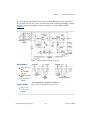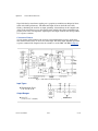
1
Signal Conditioning SC-2311 User Manual Connectivity for 5B and SSR Modules SC-2311 User Manual February 2001 Edition Part Number 322906A-01 Support Worldwide Technical Support and Product Information ni.com National Instruments Corporate Headquarters 11500 North Mopac Expressway Austin, Texas 78759-3504 USA Tel: 512 794 0100 Worldwide Offices Australia 03 9879 5166, Austria 0662 45 79 90 0, Belgium 02 757 00 20, Brazil 011 284 5011, Canada (Calgary) 403 274 9391, Canada (Ottawa) 613 233 5949, Canada (Québec) 514 694 8521, Canada (Toronto) 905 785 0085, China (Shanghai) 021 6555 7838, China (ShenZhen) 0755 3904939, Denmark 45 76 26 00, Finland 09 725 725 11, France 01 48 14 24 24, Germany 089 741 31 30, Greece 30 1 42 96 427, Hong Kong 2645 3186, India 91805275406, Israel 03 6120092, Italy 02 413091, Japan 03 5472 2970, Korea 02 596 7456, Mexico 5 280 7625, Netherlands 0348 433466, New Zealand 09 914 0488, Norway 32 27 73 00, Poland 0 22 528 94 06, Portugal 351 1 726 9011, Singapore 2265886, Spain 91 640 0085, Sweden 08 587 895 00, Switzerland 056 200 51 51, Taiwan 02 2528 7227, United Kingdom 01635 523545 For further support information, see the Technical Support Resources appendix. To comment on the documentation, send e-mail to [email protected] Copyright © 2001 National Instruments Corporation. All rights reserved. Important Information Warranty The SC-2311 shielded carrier, SSR Series modules, and 5B Series modules are warranted against defects in materials and workmanship for a period of one year from the date of shipment, as evidenced by receipts or other documentation. National Instruments will, at its option, repair or replace equipment that proves to be defective during the warranty period. This warranty includes parts and labor. The media on which you receive National Instruments software are warranted not to fail to execute programming instructions, due to defects in materials and workmanship, for a period of 90 days from date of shipment, as evidenced by receipts or other documentation. National Instruments will, at its option, repair or replace software media that do not execute programming instructions if National Instruments receives notice of such defects during the warranty period. National Instruments does not warrant that the operation of the software shall be uninterrupted or error free. A Return Material Authorization (RMA) number must be obtained from the factory and clearly marked on the outside of the package before any equipment will be accepted for warranty work. National Instruments will pay the shipping costs of returning to the owner parts which are covered by warranty. National Instruments believes that the information in this document is accurate. The document has been carefully reviewed for technical accuracy. In the event that technical or typographical errors exist, National Instruments reserves the right to make changes to subsequent editions of this document without prior notice to holders of this edition. The reader should consult National Instruments if errors are suspected. In no event shall National Instruments be liable for any damages arising out of or related to this document or the information contained in it. EXCEPT AS SPECIFIED HEREIN, NATIONAL INSTRUMENTS MAKES NO WARRANTIES, EXPRESS OR IMPLIED, AND SPECIFICALLY DISCLAIMS ANY WARRANTY OF MERCHANTABILITY OR FITNESS FOR A PARTICULAR PURPOSE. CUSTOMER’S RIGHT TO RECOVER DAMAGES CAUSED BY FAULT OR NEGLIGENCE ON THE PART OF NATIONAL INSTRUMENTS SHALL BE LIMITED TO THE AMOUNT THERETOFORE PAID BY THE CUSTOMER. NATIONAL INSTRUMENTS WILL NOT BE LIABLE FOR DAMAGES RESULTING FROM LOSS OF DATA, PROFITS, USE OF PRODUCTS, OR INCIDENTAL OR CONSEQUENTIAL DAMAGES, EVEN IF ADVISED OF THE POSSIBILITY THEREOF. This limitation of the liability of National Instruments will apply regardless of the form of action, whether in contract or tort, including negligence. Any action against National Instruments must be brought within one year after the cause of action accrues. National Instruments shall not be liable for any delay in performance due to causes beyond its reasonable control. The warranty provided herein does not cover damages, defects, malfunctions, or service failures caused by owner’s failure to follow the National Instruments installation, operation, or maintenance instructions; owner’s modification of the product; owner’s abuse, misuse, or negligent acts; and power failure or surges, fire, flood, accident, actions of third parties, or other events outside reasonable control. Copyright Under the copyright laws, this publication may not be reproduced or transmitted in any form, electronic or mechanical, including photocopying, recording, storing in an information retrieval system, or translating, in whole or in part, without the prior written consent of National Instruments Corporation. Trademarks LabVIEW™, National Instruments™, ni.com™, and NI-PGIA™are trademarks of National Instruments Corporation. Product and company names mentioned herein are trademarks or trade names of their respective companies. WARNING REGARDING USE OF NATIONAL INSTRUMENTS PRODUCTS (1) NATIONAL INSTRUMENTS PRODUCTS ARE NOT DESIGNED WITH COMPONENTS AND TESTING FOR A LEVEL OF RELIABILITY SUITABLE FOR USE IN OR IN CONNECTION WITH SURGICAL IMPLANTS OR AS CRITICAL COMPONENTS IN ANY LIFE SUPPORT SYSTEMS WHOSE FAILURE TO PERFORM CAN REASONABLY BE EXPECTED TO CAUSE SIGNIFICANT INJURY TO A HUMAN. (2) IN ANY APPLICATION, INCLUDING THE ABOVE, RELIABILITY OF OPERATION OF THE SOFTWARE PRODUCTS CAN BE IMPAIRED BY ADVERSE FACTORS, INCLUDING BUT NOT LIMITED TO FLUCTUATIONS IN ELECTRICAL POWER SUPPLY, COMPUTER HARDWARE MALFUNCTIONS, COMPUTER OPERATING SYSTEM SOFTWARE FITNESS, FITNESS OF COMPILERS AND DEVELOPMENT SOFTWARE USED TO DEVELOP AN APPLICATION, INSTALLATION ERRORS, SOFTWARE AND HARDWARE COMPATIBILITY PROBLEMS, MALFUNCTIONS OR FAILURES OF ELECTRONIC MONITORING OR CONTROL DEVICES, TRANSIENT FAILURES OF ELECTRONIC SYSTEMS (HARDWARE AND/OR SOFTWARE), UNANTICIPATED USES OR MISUSES, OR ERRORS ON THE PART OF THE USER OR APPLICATIONS DESIGNER (ADVERSE FACTORS SUCH AS THESE ARE HEREAFTER COLLECTIVELY TERMED “SYSTEM FAILURES”). ANY APPLICATION WHERE A SYSTEM FAILURE WOULD CREATE A RISK OF HARM TO PROPERTY OR PERSONS (INCLUDING THE RISK OF BODILY INJURY AND DEATH) SHOULD NOT BE RELIANT SOLELY UPON ONE FORM OF ELECTRONIC SYSTEM DUE TO THE RISK OF SYSTEM FAILURE. TO AVOID DAMAGE, INJURY, OR DEATH, THE USER OR APPLICATION DESIGNER MUST TAKE REASONABLY PRUDENT STEPS TO PROTECT AGAINST SYSTEM FAILURES, INCLUDING BUT NOT LIMITED TO BACK-UP OR SHUT DOWN MECHANISMS. BECAUSE EACH END-USER SYSTEM IS CUSTOMIZED AND DIFFERS FROM NATIONAL INSTRUMENTS' TESTING PLATFORMS AND BECAUSE A USER OR APPLICATION DESIGNER MAY USE NATIONAL INSTRUMENTS PRODUCTS IN COMBINATION WITH OTHER PRODUCTS IN A MANNER NOT EVALUATED OR CONTEMPLATED BY NATIONAL INSTRUMENTS, THE USER OR APPLICATION DESIGNER IS ULTIMATELY RESPONSIBLE FOR VERIFYING AND VALIDATING THE SUITABILITY OF NATIONAL INSTRUMENTS PRODUCTS WHENEVER NATIONAL INSTRUMENTS PRODUCTS ARE INCORPORATED IN A SYSTEM OR APPLICATION, INCLUDING, WITHOUT LIMITATION, THE APPROPRIATE DESIGN, PROCESS AND SAFETY LEVEL OF SUCH SYSTEM OR APPLICATION. Conventions The following conventions appear in this manual: This icon denotes a note, which alerts you to important information. This icon denotes a caution, which advises you of precautions to take to avoid injury, data loss, or a system crash. bold Bold text denotes items that you must select or click on in the software, such as menu items and dialog box options. Bold text also denotes parameter names. italic Italic text denotes variables, emphasis, a cross reference, or an introduction to a key concept. This font also denotes text that is a placeholder for a word or value that you must supply. monospace Text in this font denotes text or characters that you should enter from the keyboard, sections of code, programming examples, and syntax examples. This font is also used for the proper names of disk drives, paths, directories, programs, subprograms, subroutines, device names, functions, operations, variables, filenames and extensions, and code excerpts. Contents Chapter 1 Introduction About the SC-2311, 5B Series Modules, and SSR Series Modules ..............................1-2 What You Need to Get Started ......................................................................................1-3 Unpacking ......................................................................................................................1-4 Chapter 2 Configuring and Setting Up the SC-2311 Configuring the SC-2311...............................................................................................2-1 Setting SW5.....................................................................................................2-4 Setting SW4.....................................................................................................2-4 Setting SW3.....................................................................................................2-4 Setting SW2.....................................................................................................2-5 Safety Information .........................................................................................................2-5 Using the I/O Panelettes ................................................................................................2-7 I/O Panelette Labels ........................................................................................2-8 Mounting the SC-2311...................................................................................................2-9 Chapter 3 5B Series Modules Overview........................................................................................................................3-1 5B30, 5B31, 5B40, 5B41 Voltage Input Module ..........................................................3-2 5B32 Process Current Input Module .............................................................................3-2 5B34 RTD Input—Isolated 2- or 3-Wire RTD Module ................................................3-2 5B35 RTD Input—Isolated 4-Wire RTD Module .........................................................3-3 5B36 Potentiometer Input Module ................................................................................3-3 5B37 Thermocouple Input Module with Cold-Junction Compensation........................3-3 5B38 Strain-Gauge Input Module..................................................................................3-4 5B42 Process Current Input Module with 20 VDC Loop .............................................3-4 5B45/46 Frequency Input Module .................................................................................3-4 5B47 Linearized Thermocouple Input Module with Cold-Junction Compensation......3-5 © National Instruments Corporation v SC-2311 User Manual Contents Chapter 4 SSR Series Modules Overview ....................................................................................................................... 4-1 Input Modules................................................................................................................ 4-1 SSR-IAC-5, 120 VAC..................................................................................... 4-2 SSR-IAC-5A, 240 VAC.................................................................................. 4-2 SSR-IDC-5, 3–32 VDC................................................................................... 4-3 Output Modules ............................................................................................................. 4-3 SSR-OAC-5, 120 VAC ................................................................................... 4-4 SSR-OAC-5A, 240 VAC ................................................................................ 4-5 SSR-ODC-5, 3–60 DVC ................................................................................. 4-5 Appendix A Specifications Appendix B 5B Series Module Data Sheets Appendix C Power Requirements for the SC-2311 with 5B and SSR Series Modules Appendix D Technical Support Resources Glossary Index SC-2311 User Manual vi ni.com Contents Figures Figure 2-1. Figure 2-2. Figure 2-3. Figure 2-4. Figure 2-5. Figure 2-6. Figure 2-7. SC-2311 Top Cover Removal ...............................................................2-2 SC-2311 Parts Locator Diagram ...........................................................2-3 NRSE, and RSE or DIFF Mode Circuits...............................................2-4 Installing an I/O Panelette .....................................................................2-8 Installing an I/O Panelette Label ...........................................................2-9 Rack-Mount Option...............................................................................2-10 Stack-Mount Option ..............................................................................2-11 Figure 4-1. Figure 4-2. Figure 4-3. Figure 4-4. SSR-IAC AC Input Diagram.................................................................4-2 SSR-IDC DC Input Diagram.................................................................4-3 SSR-OAC AC Output Diagram ............................................................4-4 SSR-ODC DC Output Diagram ............................................................4-6 Tables Table C-1. Table C-2. 5B Series Current Requirements ...........................................................C-1 SSR Series Current Requirements.........................................................C-2 © National Instruments Corporation vii SC-2311 User Manual 1 Introduction This manual describes the electrical and mechanical aspects of the SC-2311 shielded carrier, 5B Series modules, SSR Series modules, and accessory terminal blocks. It also describes how to configure, connect, and customize the SC-2311 for use with National Instruments E Series data acquisition (DAQ) devices. The SC-2311 shielded carrier interfaces with the following signal conditioning modules: • • © National Instruments Corporation Analog signal conditioning – 5B30, 5B31, 5B40, 5B41 voltage input modules – 5B32 process-current input modules – 5B34 RTD input, isolated 2- or 3-wire RTD modules – 5B35 RTD input, isolated 4-wire RTD modules – 5B36 potentiometer input modules – 5B37 thermocouple input with cold-junction compensation modules – 5B42 process-current input with regulated 20 VDC loop modules – 5B47 linearized thermocouple input with cold-junction compensation modules – 5B38 strain-gauge input modules – 5B45/46 frequency input modules Digital signal conditioning – SSR-IAC-5 input module (120 VAC) – SSR-IAC-5A input module (240 VAC) – SSR-IDC-5 input module (3 to 32 VDC) – SSR-OAC-5 output module (120 VAC) – SSR-OAC-5A output module (240 VAC) – SSR-ODC-5 output module (3 to 60 VDC) 1-1 SC-2311 User Manual Chapter 1 Introduction About the SC-2311, 5B Series Modules, and SSR Series Modules This section describes the SC-2311 shielded carrier, 5B Series modules, and SSR Series modules. It also lists what you need to get started, and explains how to unpack your SC-2311 and signal conditioning modules. The SC-2311 connects signals to E Series DAQ devices. The SC-2311 can interface up to eight 5B Series modules and eight SSR Series modules simultaneously. When used with the 5B Series modules, SSR Series modules, and a shielded 68-pin E Series cable, the SC-2311 offers a clean, easy-to-use solution to analog and digital signal conditioning that is both portable and rugged. The SC-2311 also provides 50 terminal block connections for non-isolated measurements. This feature allows you direct access to the I/O signals from the E Series DAQ device. The SC-2311 has internal terminal blocks for connecting to the 5B Series modules as well as the SSR Series modules. The SC-2311 allows you to optimize connectivity to the terminal blocks through the use of panelettes. The SC-2311 shielded carrier has a portable enclosure, and is ideal for laptop and desktop applications. The 5B Series modules along with the SC-2311 provide a high-performance, inexpensive means of analog signal conditioning. You can insert the 5B Series modules into any of the eight available slots on the carrier. The 5B Series modules, along with the SC-2311, provide analog input measurements such as voltage, current, resistance, temperature, strain, and frequency. The SSR Series modules along with the SC-2311 provide an easy-to-use means of digitally controlling or sensing voltages from field devices. The SSR Series modules are high-performance, fully encapsulated devices that you can insert into any of the eight available slots on the SC-2311. The SC-2311 also has light emitting diodes (LEDs) that indicate the status of each SSR Series module. SC-2311 User Manual 1-2 ni.com Chapter 1 Introduction What You Need to Get Started To set up and use the SC-2311 you need the following items: ❑ SC-2311 shielded carrier ❑ Up to eight of the following 5B Series modules for analog signal conditioning – 5B30/31 – 5B32 – 5B34 – 5B35 – 5B36 – 5B37 – 5B38 – 5B40/41 – 5B42 – 5B45/46 – 5B47 ❑ Up to eight of the following SSR Series modules for digital signal conditioning – SSR-IAC-5 – SSR-IAC-5A – SSR-IDC-5 – SSR-OAC-5 – SSR-OAC-5A – SSR-ODC-5 ❑ SC-2311 User Manual ❑ External power supply (supplied) ❑ 68-pin E Series DAQ device, documentation, and 68-pin E Series cable ❑ Flathead screwdriver 0.1 in. (supplied) ❑ Number 1 and 2 Phillips-head screwdrivers © National Instruments Corporation 1-3 SC-2311 User Manual Chapter 1 Introduction ❑ Wire-insulation strippers ❑ NI-DAQ 6.9 or later (driver software) ❑ One or more I/O panelettes and label sheet Unpacking Your SC-2311 shielded carrier is shipped in a cardboard box. The 5B and SSR Series modules are shipped in antistatic packaging to prevent electrostatic damage to the modules. Electrostatic discharge can damage several components on these products. To avoid such damage when you handle the products, take the following precautions: Caution • Ground yourself by using a grounding strap or by touching a grounded object. • Touch the antistatic package to a metal part of your computer chassis before removing the modules from the packaging. Never touch the exposed pins of connectors. • SC-2311 User Manual Remove the modules from the packaging and inspect the modules for any sign of damage. Notify National Instruments if the modules appear damaged in any way. Do not install a damaged module into your system. 1-4 ni.com Configuring and Setting Up the SC-2311 2 This chapter explains how to configure the SC-2311, provides safety information, and explains how to install I/O panelettes and mounting accessories. Configuring the SC-2311 The SC-2311 contains the following slide switches that are used to configure the device: • SW5 • SW4 • SW3 • SW2 You must configure these slide switches prior to operating the SC-2311. To access the slide switches, remove the eight top cover screws and the top cover as shown in Figure 2-1. See Figure 2-2 for switch locations. © National Instruments Corporation 2-1 SC-2311 User Manual Chapter 2 Configuring and Setting Up the SC-2311 1 2 3 1 Top Cover Screws 2 Top Cover 3 SC-2311 Figure 2-1. SC-2311 Top Cover Removal SC-2311 User Manual 2-2 ni.com Chapter 2 1 2 3 4 5 Configuring and Setting Up the SC-2311 6 7 1 2 SW5 SW4 3 4 SW3 5B Series Modules 5 6 SSR Series Modules SW2 7 Safety Ground Figure 2-2. SC-2311 Parts Locator Diagram © National Instruments Corporation 2-3 SC-2311 User Manual Chapter 2 Configuring and Setting Up the SC-2311 Setting SW5 Setting SW5 to the AIGND/AISENSE SHORT position allows the E Series DAQ device to operate in nonreferenced single-ended (NRSE) mode. Use this switch setting when you are using 5B Series modules to take measurements. In this mode, AIGND connects the negative input to the PGIA on the E Series DAQ device through the AISENSE pin as shown in Figure 2-3. SC-2311 5B ACH0 Analog Multiplexer +5V (DIFF) INX+ (NRSE) ACHX INX– E Series DAQ Device in NRSE Mode NI-PGIA Gain Amplifier + ACH15 AIGND AISENSE SW5 – AIGND Figure 2-3. NRSE, and RSE or DIFF Mode Circuits When the E Series DAQ device operates in referenced single-ended (RSE) or differential (DIFF) mode, set SW5 to NC. When SW5 is in the NC position it breaks the connection between AISENSE and AIGND as shown in Figure 2-3. Use this setting if you are not using 5B modules to take measurements. Setting SW4 Setting SW4 to the SPLY GND/AIGND SHORT position allows the 5B Series modules to function properly when using the external power supply. This switch setting short circuits the external supply ground to the AIGND of the E Series DAQ device. In most cases, SW4 should remain in the SPLY GND/AIGND SHORT position. Setting SW3 Setting SW3 to the EXT +5V (5B) position powers the 5B modules using the external power supply. In this mode, it is necessary to connect the external power supply to power the 5B Series modules. For the best performance, set SW3 to the EXT +5V (5B) position and use the external power supply. SC-2311 User Manual 2-4 ni.com Chapter 2 Configuring and Setting Up the SC-2311 Setting SW3 to the Board +5V (5B) position powers the 5B modules using the E Series DAQ device +5 V supply. In this mode, you can power the 5B Series modules directly from the E Series DAQ device. The maximum current that the DAQ device can deliver depends on which DAQ device you have selected. When using the Board +5V (5B) setting, it is necessary to know the current requirements of the 5B Series modules and the current available from the DAQ device you are using. See Appendix C, Power Requirements for the SC-2311 with 5B and SSR Series Modules, for more details. Note Setting SW2 Setting SW2 to the EXT +5V (SSR) position powers the SSR modules using the external power supply. In this mode, you must connect the external power supply to power the SSR Series modules. Setting SW2 to the Board +5V (SSR) position powers the SSR modules using the E Series DAQ device +5 V supply. In this mode, you can power the SSR Series modules directly from the E Series DAQ device. The maximum current that the DAQ device can deliver depends on which DAQ device you have selected. When using the Board +5V (SSR) setting, it is necessary to know the current requirements of the SSR Series modules and the current available from the DAQ device you are using. Note Safety Information Cautions Do not operate the device in an explosive atmosphere or where there may be flammable gases or fumes. Keep away from live circuits. Do not remove equipment covers or shields unless you are trained to do so. If signal wires are connected to the device, hazardous voltages can exist even when the equipment is turned off. To avoid a shock hazard, do not perform procedures involving cover or shield removal unless you are qualified to do so and disconnect all field power prior to removing covers or shields. Equipment described in this document must be used in an Installation Category II1 environment per IEC 60664-1. Do not operate damaged equipment. The safety protection features built into this device 1 Category II refers to local-level power distribution, such as that provided by a standard wall outlet. © National Instruments Corporation 2-5 SC-2311 User Manual Chapter 2 Configuring and Setting Up the SC-2311 can become impaired if the device becomes damaged in any way. If the device is damaged, turn the device off and do not use it until service-trained personnel can check its safety. If necessary, return the device to National Instruments for service and repair to ensure that its safety is not compromised. Do not operate this equipment in a manner that contradicts the information specified in this document. Misuse of this equipment could result in a shock hazard. Do not substitute parts or modify equipment. Because of the danger of introducing additional hazards, do not install unauthorized parts or modify the device. Return the device to National Instruments for service and repair to ensure that its safety features are not compromised. You must insulate all of your signal connections to the highest voltage with which the SC-2311 can come in contact. When using the device with high common-mode voltages, you must insulate your signal wires for the highest input voltage. National Instruments is not liable for any damages or injuries resulting from inadequate signal wire insulation. Use only 26–14 AWG wire with a minimum voltage rating of 300 V and a temperature value of 60 °C for measuring up to 300 V. When connecting or disconnecting signal lines to the SC-2311 screw terminals, make sure the lines are powered off. Potential differences between the lines and the SC-2311 ground can create a shock hazard while you connect the lines. Connections, including power signals to ground and vice versa, that exceed any of the maximum signal ratings on the SC-2311 device can create a shock or fire hazard, or can damage any or all of the boards connected to the SC-2311, the host computer, and the SC-2311 device. National Instruments is not liable for any damages or injuries resulting from incorrect signal connections. If hazardous voltages (≥30 Vrms and 42.4 Vpeak or 60 VDC) are present, you must connect a safety earth-ground wire to the safety-ground screw terminal, shown in Figure 2-2. This complies with safety agency requirements and protects against electric shock when the SC-2311 is not connected to an installed DAQ device. To connect the safety earth-ground to the safety-ground screw terminal, run an earth-ground wire from the signal source to the screw terminal. National Instruments is not liable for any damages or injuries resulting from inadequate safety earth-ground connections. Clean the SC-2311 and accessories by brushing off light dust with a soft nonmetallic brush. Remove other contaminants with a stiff nonmetallic brush. The unit must be completely dry and free from contaminants before returning it to service. SC-2311 User Manual 2-6 ni.com Chapter 2 Configuring and Setting Up the SC-2311 Using the I/O Panelettes Select configurable I/O panelettes appropriate for the I/O connectivity needs of your application. The I/O panelettes have standard prewired I/O connectors. You can install I/O panelettes on the front of the SC-2311 enclosure. You can install up to 18 single-width I/O panelettes in the SC-2311 enclosure. You can mix all types of I/O panelettes to produce custom I/O combinations. The strain-relief and 9-pin D-subminiature I/O panelettes require two panelette spaces. The dual 9-pin D-sub I/O panelette requires three panelette spaces. Note Each thermocouple and BNC I/O panelette accommodates two connectors. Use the strain-relief I/O panelettes to connect large numbers of wires directly to your internal accessory. You can machine the blank I/O panelettes to make custom I/O panelettes to suit your application. Use the preconfigured I/O panelettes to quickly connect and disconnect standard connectors. Note For RF emission compliance, you cannot use BNC panelettes. Refer to Figure 2-4 and use the following steps to install any of the I/O panelettes: 1. Choose one of the I/O panelettes to install. 2. Place the lower edge of the I/O panelette in the groove at the bottom of the enclosure opening. 3. Tilt the I/O panelette top back into the enclosure. 4. Secure the I/O panelette with either one, two, or three of the M2.5 × 6 panhead screws (depending on the type of I/O panelette) that are included with the panelette. 5. Repeat steps 1 through 4 until you have installed all your non-blank I/O panelettes. 6. Install a blank I/O panelette in any unused panelette opening. © National Instruments Corporation 2-7 SC-2311 User Manual Chapter 2 Configuring and Setting Up the SC-2311 L S A T N EN IO UM AT R N ST IN S di on lC na ig ng ni tio ith w fig on 1 31 tors -2 nec C Con S urable C 1 2 4 3 5 6 7 1 2 3 Thermocouple I/O Panelette M2.5 × 6 Screw BNC I/O Panelette 4 5 Strain-Relief I/O Panelette D-Sub I/O Panelette 6 7 Dual D-Sub I/O Panelette Blank I/O Panelette Figure 2-4. Installing an I/O Panelette I/O Panelette Labels Each SC-2311 ships with a sheet of labels for you to apply to your I/O panelettes as shown in Figure 2-5. The label sheet has both preprinted and blank labels. You can customize the blank labels to suit your application. You can use two labels on single-width I/O panelettes and three or more labels on wider panelettes. Caution SC-2311 User Manual Do not use a panelette for signals that exceed the panelette rating. 2-8 ni.com Chapter 2 Configuring and Setting Up the SC-2311 2 1 1 I/O Panelette 2 Label Figure 2-5. Installing an I/O Panelette Label Mounting the SC-2311 To install your SC-2311 enclosure in a standard 19 in. rack, install the optional rack-mount kit. To use your SC-2311 enclosure in a desktop stacking configuration install the optional stack-mount kit. Refer to Figure 2-6 and use the following steps to install the rack-mount kit on your SC-2311 enclosure: 1. Attach a rack-mount bracket to one side of the enclosure with four 4-40 × 1/4 in. screws from the rack-mount kit. 2. Attach a rack-mount bracket to the other side of the enclosure with four 4-40 × 1/4 in. screws from the rack-mount kit. You must remove the rubber feet from the bottom of the SC-2311 enclosure for use in rack-mount applications. Note © National Instruments Corporation 2-9 SC-2311 User Manual Chapter 2 Configuring and Setting Up the SC-2311 L S A T N EN IO UM AT R N ST IN N INSATION TR AL UM EN TS g in on ti di on lC na ig S ith w le ab ur fig on C SC -23 s or ct ne on C 11 2 N INSATION TR AL UM EN TS 1 1 4-40 x 1/4 in. Screws 2 Rack-Mount Brackets Figure 2-6. Rack-Mount Option Refer to Figure 2-7 and use the following steps to install the stack-mount kit on your SC-2311 configurable connector enclosure: 1. Attach the stack-mount brackets to both ends of the lower enclosure with the 4-40 × 1/4 in. flathead screws from the stack-mount kit. 2. Place the upper enclosure on top of the lower enclosure. 3. Attach the stack-mount brackets to both ends of the upper enclosure with the 4-40 × 1/4 in. flathead screws from the stack-mount kit. You must remove the rubber feet from all but the bottom enclosure before stacking the enclosures. Note SC-2311 User Manual 2-10 ni.com Chapter 2 Configuring and Setting Up the SC-2311 1 INSNAT TR ION UM AL EN TS Sig nal Co ndit ion ing wit hC onf igu SC rab le Co -23 nne cto 11 rs 1 2 1 4-40 × 1/4 in. Flathead Screws 2 Stack-Mount Brackets Figure 2-7. Stack-Mount Option You can stack additional enclosures by using additional stack-mount kits. You can remove the stack-mount kit handles, if necessary, by removing the two screws that attach the handle. Note You can also use the stack-mounting brackets as handles. © National Instruments Corporation 2-11 SC-2311 User Manual 3 5B Series Modules This chapter describes the 5B Series modules you can use with the SC-2311. Overview You can use 5B Series modules with the SC-2311 to perform per-channel analog signal conditioning with National Instruments E Series DAQ devices. The 5B Series modules are inserted in an eight-channel backplane within the SC-2311. The 5B Series modules provide isolation, noise rejection, and amplification for millivolt sources, volt sources, 4–20 mA sources, 0–20 mA sources, RTDs, thermocouples, strain gauges, potentiometers, and frequency inputs. Install panelettes in the front of the SC-2311 to connect to your I/O signals. Connect the panelettes to the input terminal blocks of corresponding 5B channels. After the signals are conditioned, they are routed through a shielded 68-position cable to an E Series DAQ device for measurement. The 5B Series modules include the following: • 5B30, 5B31, 5B40, 5B41 voltage input modules • 5B32 process current input modules • 5B34 RTD input—isolated 2- or 3-wire RTD modules • 5B35 RTD input—isolated 4-wire RTD modules • 5B36 potentiometer input modules • 5B37 thermocouple input modules with cold-junction compensation • 5B38 strain gauge input modules • 5B42 process current input modules with regulated 20 VDC loop • 5B45/46 frequency input modules • 5B47 linearized thermocouple input modules with cold-junction compensation © National Instruments Corporation 3-1 SC-2311 User Manual Chapter 3 5B Series Modules See Appendix C, Power Requirements for the SC-2311 with 5B and SSR Series Modules, to calculate the power requirements for your 5B Series modules. 5B30, 5B31, 5B40, 5B41 Voltage Input Module The 5B Series voltage input modules can accept input measurement ranges from ±10 mV to ± 20 V. These modules scale the input voltage to a ±5 V range that is routed from the SC-2311 to the E Series DAQ device for measurement. You can insert and use the 5B Series voltage input modules in any of the eight 5B channels inside the SC-2311. 5B32 Process Current Input Module The 5B32 process current input modules can accept either 4–20 mA or 0–20 mA and scale this current to a 0–5 V signal. This measurement is accomplished by reading the voltage across a precision 20 Ω resistor that is included with the 5B32 module. These modules scale the input current to a 0–5 V output signal that is routed from the SC-2311 to the E Series DAQ device for measurement. You can insert and use the 5B32 process current input modules in any of the eight 5B channels inside the SC-2311. 5B34 RTD Input—Isolated 2- or 3-Wire RTD Module The 5B34 RTD input modules are capable of making isolated 2- or 3-wire RTD measurements and can accept a large variety of different RTD types. The 5B34 modules scale the RTD temperature measurement to a 0–5 V output signal that is routed from the SC-2311 to the E Series DAQ device for measurement. You can insert and use the 5B34 RTD input modules in any of the eight 5B channels inside the SC-2311. SC-2311 User Manual 3-2 ni.com Chapter 3 5B Series Modules 5B35 RTD Input—Isolated 4-Wire RTD Module The 5B35 RTD input modules are capable of making isolated 4-wire RTD measurements. Like the 5B34, the 5B35 scales the RTD temperature measurement into a 0–5 V output signal that the E Series DAQ device can measure. You can insert and use the 5B35 RTD input modules in any of the eight 5B channels inside the SC-2311. 5B36 Potentiometer Input Module The 5B36 potentiometer input modules accept a wide variety of 3-wire potentiometers and 2-wire rheostats. The 5B36 scales the potentiometer measurement into an accurate 0–5 V output signal that is routed from the SC-2311 to the E Series DAQ device for measurement. You can insert and use the 5B36 potentiometer input modules in any of the eight 5B channels inside the SC-2311. 5B37 Thermocouple Input Module with Cold-Junction Compensation The 5B37 thermocouple input module is capable of accepting input signals from J, K, T, E, R, S, and B type thermocouples. The 5B37 also uses cold-junction compensation circuitry, which is part of the SC-2311 accessory, to compensate for the parasitic thermocouples formed at the input screw terminals of the SC-2311. The 5B37 scales the input signals from the thermocouples into a 0–5 V output signal that is routed from the SC-2311to the E Series DAQ device for measurement. You can insert and use the 5B37 thermocouple input modules in any of the eight 5B channels inside the SC-2311. © National Instruments Corporation 3-3 SC-2311 User Manual Chapter 3 5B Series Modules 5B38 Strain-Gauge Input Module The 5B38 strain-gauge input module features a bandwidth of 10 kHz. The 5B38 accepts input signals from full- and half-bridge 300 Ω to 10 kΩ transducers. The 5B38 also provides a +10 V excitation and produces an output signal of –5 to +5 V that is routed from the SC-2311 to the E Series DAQ device for measurement. You can insert and use the 5B38 strain-gauge input modules in any of the eight 5B channels inside the SC-2311. 5B42 Process Current Input Module with 20 VDC Loop The 5B42 process current input module interfaces with 2-wire transmitters and provides an isolated, regulated 20 V supply for current measurement. The module filters and amplifies the 4–20 mA process-current input to produce an accurately scaled, low-noise, low-impedance output of +1 to +5 V or +2 to +10 V. You can insert and use the 5B42 process current input modules in any of the eight 5B channels inside the SC-2311. 5B45/46 Frequency Input Module The 5B45 frequency input modules accept full-scale frequency signals ranging from 500 Hz to 20 kHz. The 5B46 frequency input modules accept full-scale frequency signals from 20 kHz to 275 kHz. Each module scales the frequency input to a 0–5 V output signal that is routed from the SC-2311 to the DAQ device for measurement. You can insert and use the 5B45/46 frequency input modules in any of the eight 5B channels inside the SC-2311. SC-2311 User Manual 3-4 ni.com Chapter 3 5B Series Modules 5B47 Linearized Thermocouple Input Module with Cold-Junction Compensation The 5B47 linearized thermocouple input module is capable of accepting input signals from J, K, T, E, R, S, and B type thermocouples. The 5B47 also uses cold-junction compensation circuitry, which is part of the SC-2311 accessory, to compensate for the parasitic thermocouples formed at the input screw terminals of the SC-2311. The 5B47 linearly scales the thermocouples temperature into a 0–5 V signal that is routed form the SC-2311 to the E Series DAQ device for measurement. You can insert and use the 5B47 linearized thermocouple input modules in any of the eight 5B channels inside the SC-2311. © National Instruments Corporation 3-5 SC-2311 User Manual SSR Series Modules 4 This chapter describes the SSR Series modules you can use with the SC-2311. Overview SSR Series modules optically isolate field signals from the E Series DAQ device, preventing computer damage caused by overvoltage transients in your field wiring. Note All SSR Series modules use negative logic. The SSR Series modules include the following: • • Input modules – SSR-IAC-5, 120 VAC – SSR-IAC-5A, 240 VAC – SSR-IDC-5, 3 to 32 VDC Output modules – SSR-OAC-5, 120 VAC – SSR-OAC-5A, 240 VAC – SSR-ODC-5, 3 to 60 VDC See Appendix C, Power Requirements for the SC-2311 with 5B and SSR Series Modules, to find the power requirements for your SSR Series modules. Input Modules Input SSR Series modules sense voltages from a field source and return a logic value to the E Series DAQ device. If a voltage within the selected input range for the input module is present, it returns a logic low signal to the DAQ device, otherwise it returns a logic high signal. © National Instruments Corporation 4-1 SC-2311 User Manual Chapter 4 SSR Series Modules SSR-IAC-5, 120 VAC The SSR-IAC-5 input module senses 90–140 VAC/DC from a field source and converts it into a TTL logic signal. When a signal in this voltage range is detected at its input, the SSR generates a logic low signal on the corresponding DIO line of the E Series DAQ device. Otherwise, the SSR returns a logic high signal. Figure 4-1 shows the SSR-IAC circuit diagram. Rx 1 VAC 2 +Vcc 3 Input Voltage Hysterisis Circuit Current Regulating Output 4 Ground 5 Figure 4-1. SSR-IAC AC Input Diagram You can insert and use the SSR-IAC-5 in any of the eight SSR sockets inside the SC-2311. SSR-IAC-5A, 240 VAC The SSR-IAC-5A input module senses 180–280 VAC/DC from a field source and converts it into a TTL logic signal. When a signal in this voltage range is detected at its input, the SSR generates a logic low signal on the corresponding DIO line of the E Series DAQ device. Otherwise, the SSR returns a logic high signal. Figure 4-1 shows the SSR-IAC circuit diagram. You can insert and use the SSR-IAC-5A in any of the eight SSR sockets inside the SC-2311. SC-2311 User Manual 4-2 ni.com Chapter 4 SSR Series Modules SSR-IDC-5, 3–32 VDC The SSR-IDC-5 input module senses 3–32 VDC from a field source and converts it into a TTL logic signal. When a signal in this voltage range is detected at its input, the SSR generates a logic low signal on the corresponding DIO line of the E Series DAQ device. Otherwise, the SSR returns a logic high signal. Figure 4-2 shows the SSR-IDC circuit diagram. + Rx 1 VDC 2 – +Vcc 3 Input Voltage Hysterisis Circuit Current Regulating Output 4 Ground 5 Figure 4-2. SSR-IDC DC Input Diagram You can insert and use the SSR-IDC-5 in any of the eight SSR sockets inside the SC-2311. Output Modules SSR Series output modules use DIO lines on an E Series DAQ device to control external devices. If a DIO line sends a logic low signal, the output module turns on and current flows. If the DIO line sends a logic high signal, the output module turns off. SSR Series output modules are similar to conventional relays, but there are some important differences. Unlike conventional relays, solid state relays require voltage on the load side. Current needs to flow through them in the on state, or they turn off even if a logic low signal is at their input. This © National Instruments Corporation 4-3 SC-2311 User Manual Chapter 4 SSR Series Modules occurrence is referred to as dropout. If a solid state relay drops out, you must turn it off with a logic high signal before you can turn it on again. The dropout voltage and current specifications for the output modules are given in Appendix A, Specifications. For most control applications, such as controlling motors or lamps, these requirements are not difficult to meet. Another difference between these output modules and conventional relays is that they do not turn off completely. A small leakage current flows all the time, even in the off state. For most control applications, this current causes no problems. SSR-OAC-5, 120 VAC The SSR-OAC-5 output module uses a DIO line from the E Series DAQ device to switch an external 24–140 VAC load at up to 3.5 A. When the E Series DAQ device DIO line sends a logic low, this turns on the corresponding SSR-OAC-5 module and allows current to flow. If a logic high is sent, the module turns off. Figure 4-3 shows the SSR-OAC circuit diagram. Load 1 Snubber VAC Load 2 Trigger Circuit Rx + 3 DC Control – 4 Figure 4-3. SSR-OAC AC Output Diagram SC-2311 User Manual 4-4 ni.com Chapter 4 SSR Series Modules Unlike conventional relays, the SSR-OAC-5 output module has a zero voltage turn-on of the load. The SSR-OAC-5 also requires a minimum output voltage and current to remain in the on state. You can insert and use the SSR-OAC-5 in any of the eight SSR sockets inside the SC-2311. SSR-OAC-5A, 240 VAC The SSR-OAC-5A output module uses a DIO line from the E Series DAQ device to switch an external 24–280 VAC load at up to 3.5 A. When the E Series DAQ device DIO line sends a logic low, this turns on the corresponding SSR-OAC-5A module and allows current to flow. If a logic high is sent, the module turns off. You can insert and use the SSR-OAC-5A in any of the eight SSR sockets inside the SC-2311. SSR-ODC-5, 3–60 DVC The SSR-ODC-5 output module uses a DIO line from the E Series DAQ device to switch an external 3–60 VDC load at up to 3 A. When the E Series DAQ device DIO line sends a logic low, this turns on the corresponding SSR-ODC-5 module and allows current to flow. If a logic high is sent, the module turns off. Figure 4-4 shows the SSR-ODC circuit diagram. © National Instruments Corporation 4-5 SC-2311 User Manual Chapter 4 SSR Series Modules + Load 1 Voltage Spike Protection VDC – Load 2 Driver Circuit Rx + DC Control – 3 4 Figure 4-4. SSR-ODC DC Output Diagram You can insert and use the SSR-ODC-5 in any of the eight SSR sockets inside the SC-2311. SC-2311 User Manual 4-6 ni.com A Specifications All specifications are typical at 25 °C unless otherwise specified. SC-2311 Analog Inputs Number of channels ............................... Eight 5B Series modules (NRSE) inputs or Eight unconditioned differential inputs or 16 unconditioned single-ended inputs Input characteristics ............................... See Appendix B, 5B Series Module Data Sheets Digital I/O Number of channels ............................... 8 SSR Series modules or 8 unconditioned DIO lines I/O characteristics .................................. See the SSR Series section in this appendix Physical Dimensions............................................. 30.7 by 25.4 by 8.6 cm (12.1 by 10 by 3.4 in.) Weight (without modules or panelettes) ............. 2.0 kg (4.3 pounds) © National Instruments Corporation A-1 SC-2311 User Manual Appendix A Specifications for SC-2311 Environment Operating temperature ............................0 to 55 °C Storage temperature ................................–20 to 70 °C Relative humidity ...................................10 to 90% noncondensing Safety Designed in accordance with IEC61010-01, UL 3111-1, and CAN/CSA C22.2 No.1010.1 for electrical measuring and testing equipment. For use at altitudes up to 2000 m Installation Category II Pollution Degree 2 Electromagnetic Compatibility EMC/EMI ...............................................CE, C-Tick, and FCC Part 15 (Class A) Compliant Electrical emissions ................................EN 55011 Class A at 10 m FCC Part 15A above 1 GHz Electrical immunity ................................Evaluated to EN 61326-1:1997 A1:1998, Table 1 Safety ......................................................EN 61010-1 For full EMC and EMI compliance, you must operate this device with shielded cabling. See the Declaration of Conformity (DoC) for this product for any additional regulatory compliance information. To obtain the DoC for this product, click Declaration of Conformity at http://www.ni.com/hardref.nsf/. This website lists the DoCs by product family. Select the appropriate product family, followed by your product, and a link to the DoC (in Adobe Acrobat format) appears. Click the Acrobat icon to download or read the DoC. In addition, you cannot use BNC panelettes for full CE compliance. Note SC-2311 User Manual A-2 ni.com Appendix A Specifications for SSR Series SSR Series Input/Output Modules Logic levels ............................................ 0 to 5 V Input-to-output capacitance.................... 8 pF max Operating temperature............................ 0 to 55 °C Storage temperature ............................... –20 to 70 °C Maximum working voltage.................... 300 V Category II SSR Series input module characteristics Characteristic © National Instruments Corporation SSR-IDC-5 SSR-IAC-5 SSR-IAC-5A Nominal input 5 VDC 120 VAC 240 VAC Voltage range 3–32 VDC 90–140 VAC 180–280 VAC Voltage level ON state, min OFF state, min 3 VDC 1 VDC 90 VAC 25 VAC 180 VAC 50 VAC Supply current 10 mA 10 mA 10 mA Input impedance 1.8 kΩ 22 kΩ 60 kΩ Delay time Turn-on, max Turn-off, max 0.20 mS 0.40 mS 20 mS 20 mS 20 mS 20 mS A-3 SC-2311 User Manual Appendix A Specifications for SSR Series SSR Series output module characteristics Characteristic SSR-ODC-5 SSR-OAC-5 SSR-OAC-5A Voltage range 3–60 VDC 24–140 VAC 24–280 VAC Voltage drop 0.9 V at 3.25 A 1.2 V at 2.0 A 1.2 V at 2.0 A Current rating (one module populated) 3.25 A at 25 °C 2.8 A at 40 °C 2.25 A at 55 °C 2.0 A at 25 °C 1.6 A at 40 °C 1.1 A at 55 °C 2.0 A at 25 °C 1.6 A at 40 °C 1.1 A at 55 °C Current rating (four modules populated) 2.75 A at 25 °C 2.35 A at 40 °C 2.0 A at 55 °C 1.7 A at 25 °C 1.3 A at 40 °C 0.9 A at 55 °C 1.7 A at 25 °C 1.3 A at 40 °C 0.9 A at 55 °C Current rating (eight modules populated) 2.1 A at 25 °C 1.75 A at 40 °C 0.8 A at 55 °C 1.2 A at 25 °C 0.8 A at 40 °C 0.6 A at 55 °C 1.2 A at 25 °C 0.8 A at 40 °C 0.6 A at 55 °C Supply current 10 mA 10 mA 10 mA Leakage current, max 1.5 mA 2.0 mA 4.0 mA 0.20 µS 0.40 µS 8.33 mS 8.33 mS 8.33 mS 8.33 mS Delay time Turn-on, max Turn-off, max 5B Series For 5B Series modules specifications, see Appendix B, 5B Series Module Data Sheets. Maximum working voltage ....................300 V Category II SC-2311 User Manual A-4 ni.com 5B Series Module Data Sheets B This appendix contains the manufacturing data sheets of Analog Devices Corporation1. The Analog Devices 5B Series modules data sheets included are the following: 1 • 5B30 • 5B31 • 5B32 • 5B34 • 5B35 • 5B36 • 5B37 • 5B38 • 5B40 • 5B41 • 5B42 • 5B45 • 5B46 • 5B47 Copyright Analog Devices, Inc. 1995-2000. Reprinted with permission of the copyright owner. All rights reserved. Analog Devices, Inc. from Analog Devices Web Site www.analog.com. © National Instruments Corporation B-1 SC-2311 User Manual Appendix B 5B Series Module Data Sheets 5B30/5B31 Millivolt and Voltage Input Functional Description The 5B30 and 5B31 are single-channel signal conditioning modules that amplify, protect, filter and isolate analog input voltages. The 5B30 and 5B31 protect the computer side from damage due to field-side overvoltage faults. All models withstand 240 V rms at their input terminals without damage thereby shielding computer-side circuitry from field-side overvoltage conditions. In addition, 5B30 and 5B31 Series modules are mix-and-match and hot swappable, so can be inserted or removed from any socket in the same backplane without disrupting system power. Inside 5B30/5B31 Modules A chopper-stabilized input amplifier provides low drift and stable gain. At the amplifier input, a stable, laser-trimmed zero-scale input voltage is subtracted from the input signal to set the zero-scale value. For user convenience, the zero can be optionally factory-set to meet custom needs. This allows suppression of a zero-scale input value many times larger Internal multi-pole lowpass filtering with a four-Hz cutoff (-3dB) enhances normal-mode (noise on signal) and common-mode (noise on signal return) rejection at 50/60 Hz, enabling accurate measurement of small signals in high electrical noise. Signal isolation by transformer coupling uses a proprietary modulation technique for linear, stable and reliable performance. The differential input circuit on the field side is fully floating, eliminating the need for any input grounding. A demodulator on the computer side of the signal transformer recovers the original signal, which is then filtered and buffered to provide a low-noise, low-impedance output signal. The output common must be kept within ±3 V of power common. SC-2311 User Manual B-2 ni.com Appendix B 5B Series Module Data Sheets Convenience Features A series output switch eliminates the need for external multiplexing in many applications. The switch is turned on by an active-low enable input. The enable input should be grounded to power common if the output need not be switched. Figure 1. 5B30 and 5B31 Functional Block Diagram Input Ranges 5B30 mV Input: ±10 to ±100 mV (±5 to ±500 mV - custom) 5B31 V Input: ±1 to ±20 V (±0.5 to ±20 V - custom) Figure 2. 5B30 and 5B31 Input Field Connections Output Ranges 5B30/5B31: -5 V to +5 V or 0 to +5 V © National Instruments Corporation B-3 SC-2311 User Manual Appendix B 5B Series Module Data Sheets 5B30 and 5B31 Specifications Description Model 5B30 Model 5B31 Standard Ranges ±10 mV to ±100 mV ±1 V to ±20 V Custom Ranges ±5 mV to ±500 mV ±0.5 V to ±20 V -5 V to +5 V or 0 V to +5 V * Input Ranges Output Ranges (RL > 50 k )4 Accuracy2 Initial @ +25˚C ±0.05% Span ±10 µV RTI ±0.05% ±0.05% Span ±0.2 mV RTI (Vz1) ±0.05% (Vz1) Nonlinearity ±0.02% Span * Input Offset vs. Temperature ±1 µV/˚C ±20 µV/˚C Output Offset vs. Temperature ±20 µV/˚C * Gain vs. Temperature ±25 ppm of Reading/˚C ±50 ppm of Reading/˚C Input Bias Current ±3 nA ±0.2 nA Power On 5M 650 k Power Off 40 k 650 k Overload 40 k 650 k Input Resistance Noise Input, 0.1 Hz to 10 Hz Bandwidth 0.2 µV rms 2 µV rms Output, 100 kHz Bandwidth 200 µV rms * Bandwidth, -3 dB 4 Hz * Output Rise Time, 10% to 90% Span 200 ms * Input-to-Output, Continuous 1500 V rms maximum * Output-to-Power, Continuous ±3 V maximum * Transient ANSI/IEEE C37.90.1-1989 * Common-Mode Voltage (CMV)3 Common-Mode Rejection (CMR) 1k Source Imbalance, 50/60 Hz 160 dB (all ranges) Normal Mode Rejection, 50/60 Hz SC-2311 User Manual 60 dB 160 dB (span < ±2 V) 150 dB (span = ±10 V) * B-4 ni.com Appendix B 5B Series Module Data Sheets Input Protection Continuous 240 V rms maximum * Transient ANSI/IEEE C37.90.1-1989 * 50 * Voltage Output Protection Continuous Short to Ground * Output Selection Time 6 µs @ Cload = 0 to 2,000 pF * Max Logic "0" +1 V * Min Logic "1" +2.5 V * Max Logic "1" +36 V * Input Current "0" 0.4 mA * Power Supply Voltage +5 V ±5% * Power Supply Current 30 mA * Power Supply Sensitivity, RTI ±2 µV/Vs% ±0.4 mV/Vs% Mechanical Dimensions 2.275" x 2.375" x 0.595" (57.8 mm x 59.1 mm x 15.1 mm) * Rated Performance -25˚C to +85˚C * Operating -40˚C to +85˚C * Storage -40˚C to +85˚C * Output Resistance4 Output Enable Control Environmental Temperature Range Relative Humidity 0 to 93% @ +40˚C noncondensing * RFI Susceptibility ±0.5% Span error @ 400 MHz, 5 Watt, 3 ft * * Specifications same as model 5B30. 1 Vz is the nominal input voltage that results in a 0 V output. 2 Includes the combined effects of repeatability, hysteresis, and nonlinearity and assumes RL > 50 k . 3 The output common must be kept within ±3 V of power common. 4 Loads heavier than 50 k will degrade nonlinearity and gain temperature coefficient. Specifications subject to change without notice. Copyright 1995-2000 Analog Devices, Inc. All rights reserved. © National Instruments Corporation B-5 SC-2311 User Manual Appendix B 5B Series Module Data Sheets 5B32 Isolated Current Input Functional Description The 5B32 is a single-channel signal conditioning module that amplifies, protects, filters and isolates its analog input. The module measures a process-current input signal of 4-20 mA or 0-20 mA by reading the voltage across an external precision 20 resistor (supplied) and generating an output of 0 to +5 V. Extra current conversion resistors are available as accessories (See Model AC1362 in the Accessories section). Note that the 5B32 module circuitry can withstand 240 V rms at the input screw-terminals, thereby shielding computer-side circuitry from field-side overvoltage conditions. In addition, all 5B32 Series modules are mix-and-match and hot swappable, so can be inserted or removed from any socket in the same backplane without powering down the system. Inside the 5B32 Series Module A chopper-stabilized input amplifier provides low drift and stable gain. At the amplifier input, a stable, laser-trimmed zero-scale input offset is subtracted from the input signal to set the zero-scale value for the 4-20 mA range. For user convenience, the zero can be optionally factory-set to meet custom needs. This allows suppression of a zero-scale input value many times larger than the total span for precise expanded-scale measurements. Internal multi-pole lowpass filtering with a four-Hz cutoff (-3dB) enhances normal-mode (noise on signal) and common-mode (noise on signal return) rejection at 50/60 Hz, enabling accurate measurement of small signals in high electrical noise. Signal isolation by transformer coupling uses a proprietary modulation technique for linear, stable and reliable performance. The differential input circuit on the field side is fully floating, eliminating the need for input grounding. A demodulator on the computer side of the signal transformer recovers the original signal, which is then filtered and buffered to provide a low-noise, low-impedance output signal. The output common must be kept within ±3 Vdc of power common. SC-2311 User Manual B-6 ni.com Appendix B 5B Series Module Data Sheets Convenience Features A series output switch eliminates the need for external multiplexing in many applications. The switch is turned on by an active-low enable input. If the switch is to be on at all times, the enable-input should be grounded to power common as it is on the 5B01 and 5B08 backplanes. Figure 1. 5B32 Functional Block Diagram Input Ranges 4 mA to 20 mA Output Ranges 0 to +5 V (-5 V to +5 V - custom) Figure 2. 5B32 Input Field Connections © National Instruments Corporation B-7 SC-2311 User Manual Appendix B 5B Series Module Data Sheets 5B32 Specifications Description Model 5B32 Input Ranges Standard Ranges 0 mA to 20 mA or 4 mA to 20 mA Custom Ranges Output Ranges (RL > 50 k 0 mA to 20 mA (refer to ordering section) )4 -5 V to +5 V or 0 V to +5 V Accuracy2 Initial @ +25˚C ±0.05% Span ±0.05% Iz1 Nonlinearity ±0.02% Span Input Offset vs. Temperature ±0.0025 of Iz/˚C Output Offset vs. Temperature ±20 µV/˚C Gain vs. Temperature ±0.0025% of Reading/˚C Input Resistor5 Value 20.0 Accuracy ±0.1% Stability vs. Temperature ±0.001%/˚C Noise Input, 0.1 Hz to 10 Hz Bandwidth 10 nA rms Output, 100 kHz Bandwidth 200 µV rms Bandwidth, -3 dB 4 Hz Output Rise Time, 10% to 90% Span 200 ms Common-Mode Voltage (CMV)3 Input-to-Output, Continuous 1500 V rms maximum Output-to-Power, Continuous ±3 V maximum Transient ANSI/IEEE C37.90.1-1989 Common Mode Rejection (CMR) 1k Source Imbalance, 50/60 Hz Normal Mode Rejection 50/60 Hz SC-2311 User Manual 160 dB 60 dB B-8 ni.com Appendix B 5B Series Module Data Sheets Input Protection Continuous 240 V rms maximum Transient Output Resistance4 ANSI/IEEE C37.90.1-1989 50 Voltage Output Protection Continuous Short to Ground Output Selection Time 6 µs @ Cload = 0 to 2,000 pF Output Enable Control Max Logic "0" +1 V Min Logic "1" +2.5 V Max Logic "1" +36 V Input Current "0" 0.4 mA Power Supply Voltage +5 V ±5% Power Supply Current 30 mA Power Supply Sensitivity, RTI ±2 µV/Vs% Mechanical Dimensions 2.275" x 2.375" x 0.595" (57.8 mm x 59.1 mm x 15.1 mm) Environmental Temperature Range Rated Performance -25˚C to +85˚C Operating -40˚C to +85˚C Storage -40˚C to +85˚C Relative Humidity 0 to 93% @ +40˚C noncondensing RFI Susceptibility ±0.5% Span error @ 400 MHz, 5 Watt, 3 ft 1Iz is the nominal input current that results in a 0 V output. the combined effects of repeatability, hysteresis, and nonlinearity and assumes RL > 50 k 2Includes . Does not include current-to-voltage input resistor (AC1362) error. 3The output common must be kept within ±3 V of power common. 4Loads heavier than 50 k will degrade nonlinearity and gain temperature coefficient. 5The current-to-voltage conversion resistor (AC1362) is supplied as a plug-in component for mounting external to the module. All backplanes and mounting cards provide pin sockets for mounting the AC1362 resistor. Specifications subject to change without notice. Copyright 1995-2000 Analog Devices, Inc. All rights reserved. © National Instruments Corporation B-9 SC-2311 User Manual Appendix B 5B Series Module Data Sheets 5B34 Isolated, Linearized RTD Input Functional Description The 5B34 is a single-channel signal conditioning module that amplifies,protects, filters, linearizes and isolates a wide variety of two- and three-wire RTDs. For true four-wire RTD measurements please refer to the 5B35 section. The 5B34 protects the computer side from damage due to field-side overvoltage faults. The module withstands 240 V rms at the input terminals without damage thereby shielding the internal computer-side circuitry from field-side overvoltage conditions. In addition, the 5B34 is mix-and-match and hot swappable with all other 5B Series input modules, so can be inserted or removed from any socket in the same backplane without disrupting system power. Inside the 5B32 Series Module Two identical sources provide excitation current for the RTD. For three-wire RTDs, the second current flows through the third RTD lead so as to cancel the effects of (equal) lead resistance; this current also flows through a stable resistor laser-trimmed to the RTD value that sets the differential amplifier input and (module) output to zero volts at that scale point. The current sources and the amplifier input are protected to withstand input overvoltage up to 240 V rms. A differential chopper-stabilized input amplifier provides stable gain and exceptionally low drift. This allows the use of very low RTD excitation current to minimize self-heating and preserve measurement accuracy. Along with module gain and zero settings, a feedback linearizer is laser-trimmed. Custom versions of 5B34 can be laser-trimmed to meet special requirements. Internal multi-pole lowpass filtering with a four-Hz cutoff (-3dB)enhances normal-mode (noise on signal) and common-mode (noise on signal return) rejection at 50/60 Hz, enabling accurate measurement of small signals in high electrical noise. Signal isolation by transformer coupling uses a proprietary modulation technique for linear, stable and reliable performance. The differential input circuit on the field side is fully floating, eliminating the need for any input grounding. A demodulator on the computer side of the signal transformer recovers the original signal, which is then filtered and buffered to provide a low-noise, low-impedance output signal. The output common must be kept within ±3 V of power common. SC-2311 User Manual B-10 ni.com Appendix B 5B Series Module Data Sheets Convenience Features A series output switch eliminates the need for external multiplexing in many applications. The switch is turned on by an active-low enable input. If the switch is to be on at all times, the enable-input should be grounded to power common as it is on the 5B01 and 5B08 backplanes. Figure 1. 5B34 Functional Block Diagram Input Types 100 10 120 Platinum RTD Copper RTD Nickel RTD Output Range 0 to +5 V Figure 2. 5B34 Input Field Connections © National Instruments Corporation B-11 SC-2311 User Manual Appendix B 5B Series Module Data Sheets 5B34 Specifications (typical @ +25˚C and V s = +5 V dc) Description Model 5B34 Input Ranges Standard Ranges Refer to Model Table Custom Ranges -200˚C to +850˚C (100 -80˚C to +320˚C (120 -100˚C to +260˚C (10 Output Range (RL > 50 k ) Platinum) Nickel) Copper) 0 V to +5 V Accuracy2 * ±0.05 (Rz1) Initial @ +25˚C ±0.05% Span ±0.04 Conformity Error3 ±0.05% Span Input Offset vs. Temperature ±0.02˚C/˚C Output Offset vs. Temperature ±20 µV/˚C Gain vs. Temperature ±0.005% of Reading/˚C Input Bias Current ±3 nA Input Resistance Power On 5M Power Off 40 k Overload 40 k Noise Input, 0.1 Hz to 10 Hz Bandwidth 0.2 µV rms Output, 100 kHz Bandwidth 200 µV rms Bandwidth, -3 dB 4 Hz Output Rise Time, 10% to 90% Span 200 ms Common-Mode Voltage (CMV) Input-to-Output, Continuous Output-to-Power, Continuous4 Transient 1500 V rms, maximum ±3 V, maximum ANSI/IEEE C37.90.1-1989 Common Mode Rejection (CMR) 1k Source Imbalance, 50/60 Hz Normal Mode Rejection 50/60 Hz SC-2311 User Manual 160 dB 60 dB B-12 ni.com Appendix B 5B Series Module Data Sheets Sensor Excitation Current 100 10 Pt, 120 Ni 0.25 mA 1.0 mA Cu Lead Resistance Effect 100 10 Pt, 120 Ni Cu ±0.02˚C/ ±0.2˚C/ Input Protection Continuous 240 V rms, maximum Transient ANSI/IEEE C37.90.1-1989 Output Resistance 50 Voltage Output Protection Continuous Short to Ground Output Selection Time 6 µs @ Cload = 0 to 2,000 pF Output Enable Control Max Logic "0" +1 V Min Logic "1" +2.5 V Max Logic "1" +36 V Input Current "0" 0.4 mA Power Supply Voltage +5 V ±5% Power Supply Current 30 mA Power Supply Sensitivity, RTI 100 10 Pt, 120 Ni Cu Mechanical Dimensions © National Instruments Corporation ±0.05˚C/V ±0.5˚C/V 2.275" x 2.375" x 0.595" (57.8 mm x 59.1 mm x 15.1 mm) B-13 SC-2311 User Manual Appendix B 5B Series Module Data Sheets Environmental Temperature Range Rated Performance -25˚C to +85˚C Operating -40˚C to +85˚C Storage -40˚C to +85˚C Relative Humidity 0 to 93% @ +40˚C noncondensing RFI Susceptibility ±0.5% Span error @ 400 MHz, 5 Watt, 3 ft * ±0.025 For Cu RTD's; ±0.1 For Ni RTD's. 1Rz is the value of the RTD resistance at the lowest point of the measurement range. 2Includes the combined effects of repeatability, hysteresis, and conformity error. Loads heavier than 50 k will degrade conformity and gain temperature coefficient. 3For Pt RTD's only; other types may vary. 4The output common must be kept within ±3 V of power common. Specifications subject to change without notice. Copyright 1995-2000 Analog Devices, Inc. All rights reserved. SC-2311 User Manual B-14 ni.com Appendix B 5B Series Module Data Sheets 5B35 Isolated, Linearized 4-Wire RTD Input Functional Description The 5B35 is a single-channel signal conditioning module that amplifies, filters, isolates and protects a wide variety of four-wire RTDs. The module provides a linearized, highly accurate output of 0 to +5V. Accurate and Stable Performance The four-wire configuration of the 5B35 supplies RTD excitation from a precision, protected current source: two RTD wires carry the excitation current and two wires serve as signal-input leads that measure the voltage across the RTD. Because no excitation current flows through the signal-input leads, the length or resistance of the leads creates little or no RTD measurement error. A low-drift chopper-stabilized differential amplifier allows use of very low excitation current to minimize error due to RTD self-heating. The amplifiers low input offset drift of ±0.01˚C/˚C and gain drift of ±30 ppm/˚C assure accuracy over the full operating temperature range. True Three-Port Isolation The floating, differential input circuit on the field side eliminates the need for any input grounding. Signal and power isolation by transformer coupling uses a proprietary modulation technique for linear, stable and reliable performance. A demodulator on the computer side of the signal transformer recovers the original signal, which is then filtered and buffered to provide a low-noise, low-impedance output signal. True three-port isolation (Input-Output-Power) includes common-mode ratings of : 1500 V rms between input and output and input and power; 250 V rms between power and output - no return path is required between the power and signal output commons. Filtering and Protection An optimized five-pole Butterworth filter (with a 4-Hz bandwidth) provides 116 dB of normal-mode rejection (noise on signal) at 60 Hz and 108 dB at 50 Hz. Output noise is an exceptionally low 0.3 mV p-p in a 100 kHz bandwidth and 6 mV p-p in a 5 MHz bandwidth. The 5B35 protects the computer side from damage due to field-side overvoltage faults. The module withstands 240 V rms at the input terminals without damage, thereby shielding the internal computer-side circuitry from field-side overvoltage conditions. In addition, the 5B35 is mix-and-match and hot swappable with all other 5B Series modules, so can be inserted or removed from any socket in the same backplane without disrupting system power. © National Instruments Corporation B-15 SC-2311 User Manual Appendix B 5B Series Module Data Sheets Convenience Features A series output switch eliminates the need for external multiplexing in many applications. The switch is turned on by an active-low enable input. If the switch is to be on at all times, the enable-input should be connected to output common. Figure 1. 5B35 Functional Block Diagram Input Types 100 10 120 Platinum RTD Copper RTD Nickel RTD Output Range Figure 2. 5B35 Input Field Connections 0 to +5 V SC-2311 User Manual B-16 ni.com Appendix B 5B Series Module Data Sheets 5B35 Specifications (typical @ +25˚C and Vs = +5 V dc) Description Model 5B35 Input Ranges Standard Ranges Refer to Model Table Custom Ranges -200˚C to +850˚C (100 -80˚C to +320˚C (120 -100˚C to +260˚C (10 Output Range (RL > 50 k ) Platinum, = 0.00385) Nickel, = 0.00672) Copper, = 0.004274) 0 V to +5 V Accuracy1 Initial @ +25˚C Refer to Model Table Conformity Error ±0.05% Span Input Offset vs. Temperature ±0.01˚C/˚C Output Offset vs. Temperature ±20 µV/˚C Gain vs. Temperature ±0.003% of Reading/˚C Input Resistance Power On > 1000 M Power Off 200 k Overload 200 k Noise Input, 0.1 Hz to 10 Hz Bandwidth 0.2 µV rms Output, 100 kHz Bandwidth 100 µV rms (0.3 mV peak-peak) Output, 1 MHz Bandwidth 1.5 mV peak-peak Output, 5 MHz Bandwidth 6 mV peak-peak Bandwidth, -3 dB 4 Hz Output Rise Time, 10% to 90% Span 100 ms Common-Mode Voltage (CMV) Input-to-Output, Continuous 1500 V rms, maximum Input-to-Power, Continuous 1500 V rms, maximum Output-to-Power, Continuous2 Transient © National Instruments Corporation 250 V rms, maximum ANSI/IEEE C37.90.1-1989 B-17 SC-2311 User Manual Appendix B 5B Series Module Data Sheets Common Mode Rejection (CMR) 1k Source Imbalance, 50/60 Hz Normal Mode Rejection (NMR) 190 dB (180 dB, Model 5B35-04) 116 dB @ 60 Hz; 108 dB @ 50 Hz Sensor Excitation Current 100 10 Pt, 120 Ni 0.25 mA 1.0 mA Cu Lead Resistance Effect 100 10 Pt, 120 Ni Cu ±0.00001˚C/ ±0.0001˚C/ Input Protection Continuous 240 V rms, maximum Transient ANSI/IEEE C37.90.1-1989 Output Resistance 25 Voltage Output Protection Continuous Short to Ground Output Current Limit ±9 mA Output Selection Time 6 µs to ±1 mV of Vout @ Cload = 0 to 2,000 pF Output Enable Control2 Max Logic "0" +0.8 V Min Logic "1" +2.4 V Max Logic "1" +100 V Input Current "0", "1" 0.5 µA Power Supply Voltage +5 V dc ±5% Power Supply Current 15 mA Power Supply Sensitivity, RTI ±0.2˚C/% of Vs Mechanical Dimensions 2.275" x 2.375" x 0.595" (57.8 mm x 59.1 mm x 15.1 mm) SC-2311 User Manual B-18 ni.com Appendix B 5B Series Module Data Sheets Environmental Temperature Range Rated Performance -40˚C to +85˚C Operating -40˚C to +85˚C Storage -40˚C to +85˚C Relative Humidity 0 to 93% @ +40˚C noncondensing RFI Susceptibility ±0.5% Span error @ 400 MHz, 5 Watt, 3 ft 1Includes the combined effects of repeatability, hysteresis, and conformity error. Loads heavier than 50 k will degrade conformity and gain temperature coefficient. 2The user's board layout must separate Power Common from Output Common. When the output switch is not used, connect the Enable Input to the Output Common. Output Common is connected to power common when the 5B35 is installed on a 5B Series backplane. Specifications subject to change without notice. Copyright 1995-2000 Analog Devices, Inc. All rights reserved. © National Instruments Corporation B-19 SC-2311 User Manual Appendix B 5B Series Module Data Sheets 5B36 Isolated, Potentiometer Input Functional Description The 5B36 is a single-channel signal conditioning module that amplifies, filters, and buffers a wide variety of three-wire potentiometers and two-wire rheostats (slidewires). The module provides an accurately scaled, low-noise low-impedance output of 0 to +5 V. Accurate and Stable Performance The 5B36 supplies protected potentiometer/slidewire excitation from a pair of closely matched precision current sources designed to cancel errors due to lead resistances. A low-drift chopper-stabilized differential amplifier allows use of a very low excitation current to minimize error due to potentiometer self-heating. The amplifiers low input offset drift (±0.004 /˚C) and gain drift of 30 ppm/˚C assure accuracy over the full operating temperature range. True Three-Port Isolation The floating, differential input circuit on the field side eliminates the need for any input grounding. Signal and power isolation by transformer coupling uses a proprietary modulation technique for linear, stable and reliable performance. A demodulator on the computer side of the signal transformer recovers the original signal, which is then filtered and buffered to provide a low-noise, low-impedance output signal. True three-port isolation (Input-Output-Power) includes common-mode ratings of : 1500 V rms between input-output and input-power; 250 V rms between power and output - no return path is required between the power and signal output commons. Filtering and Protection An optimized five-pole Butterworth filter (with a 4-Hz bandwidth) provides 116 dB of normal-mode rejection (noise on signal) at 60 Hz and 108 dB at 50 Hz. Output noise is an exceptionally low 0.3 mV pk-pk in a 100 kHz bandwidth and 6 mV pk-pk in a 5 MHz bandwidth. The 5B36 protects the computer side from damage due to field-side overvoltage faults. The module withstands 240 V rms at the input terminals without damage, thereby shielding the internal computer-side circuitry from field-side overvoltage conditions. In addition, the 5B36 is mix-and-match and hot swappable with all other 5B Series modules, so can be inserted or removed from any socket in the same backplane without disrupting system power. SC-2311 User Manual B-20 ni.com Appendix B 5B Series Module Data Sheets Convenience Features A series output switch eliminates the need for external multiplexing in many applications. The switch is turned on by an active-low enable input. If the switch is to be on at all times, the enable-input should be grounded to output common as it is on the 5B01 and 5B08 backplanes. Figure 1. 5B36 Functional Block Diagram Input Types Potentiometers/ Slidewires to 10k Output Range 0 to +5 V © National Instruments Corporation Figure 2. 5B36 Input Field Connections B-21 SC-2311 User Manual Appendix B 5B Series Module Data Sheets 5B36 Specifications (typical @ +25˚C and Vs = +5 V dc) Description Model 5B36 Input Ranges Standard Ranges 0 to 10 k (Refer to Model Table) Custom Ranges 0 to 10 k (Refer to Ordering Section) Output Range (RL > 50 k ) 0 V to +5 V Accuracy1 Initial @ +25˚C ±0.08% Span Input Offset vs. Temperature 100 , 500 10 k Sensor ,1k Sensors ±0.004 ±0.01 /˚C /˚C Output Offset vs. Temperature ±20 µV/˚C Gain vs. Temperature ±0.003% of Reading/˚C Input Resistance Power On > 1000 M Power Off 200 k Overload 200 k Noise Input, 0.1 Hz to 10 Hz Bandwidth 0.2 µV rms Output, 100 kHz Bandwidth 100 µV rms (0.3 mV peak-peak) Output, 1 MHz Bandwidth 1.5 mV peak-peak Output, 5 MHz Bandwidth 6 mV peak-peak Bandwidth, -3 dB 4 Hz Output Rise Time, 10% to 90% Span 100 ms SC-2311 User Manual B-22 ni.com Appendix B 5B Series Module Data Sheets Common-Mode Voltage (CMV) Input-to-Output, Continuous 1500 V rms, maximum Input-to-Power, Continuous 1500 V rms, maximum Output-to-Power, Continuous2 Transient 250 V rms, maximum ANSI/IEEE C37.90.1-1989 Common Mode Rejection (CMR) 1k Source Imbalance, 50/60 Hz Normal Mode Rejection (NMR) 170 dB 116 dB @ 60 Hz; 108 dB @ 50 Hz Sensor Excitation Current 100 , 500 10 k Sensor ,1k Sensors 0.25 mA 0.1 mA Lead Resistance Effect 100 , 500 10 k Sensor ,1k Sensors ±0.005 ±0.01 / / Input Protection Continuous 240 V rms, maximum Transient ANSI/IEEE C37.90.1-1989 Output Resistance 25 Voltage Output Protection Continuous Short to Ground Output Current Limit ±9 mA Output Selection Time 6 µs to ±1 mV of Vout @ Cload = 0 to 2,000 pF Output Enable Control2 Max Logic "0" +0.8 V Min Logic "1" +2.4 V Max Logic "1" +100 V Input Current "0", "1" 0.5 µA Power Supply Voltage +5 V dc ±5% Power Supply Current 15 mA Power Supply Sensitivity, RTI ±2 µV/% of Vs Mechanical Dimensions 2.275" x 2.375" x 0.595" (57.8 mm x 59.1 mm x 15.1 mm) © National Instruments Corporation B-23 SC-2311 User Manual Appendix B 5B Series Module Data Sheets Environmental Temperature Range Rated Performance -40˚C to +85˚C Operating -40˚C to +85˚C Storage -40˚C to +85˚C Relative Humidity 0 to 93% @ +40˚C noncondensing RFI Susceptibility ±0.5% Span error @ 400 MHz, 5 Watt, 3 ft * ±0.025 For Cu RTD's; ±0.1 For Ni RTD's. 1Includes the combined effects of repeatability, hysteresis, and nonlinearity error. Loads heavier than 50 k will degrade nonlinearity and gain temperature coefficient. 2The user's board layout must separate Power Common from Output Common. When the output switch is not used, connect the Enable Input to the Output Common. Output Common is connected to power common when the 5B36 is installed on a 5B Series backplane. Specifications subject to change without notice. Copyright 1995-2000 Analog Devices, Inc. All rights reserved. SC-2311 User Manual B-24 ni.com Appendix B 5B Series Module Data Sheets 5B37 Isolated Thermocouple Input Functional Description The 5B37 is a single-channel signal conditioning module that interfaces, amplifies and filters J, K, T, E, R, S, N, and C-type thermocouple and provides an isolated and protected precision output of 0 to +5 V. Accurate and System-Ready Internal cold-junction compensation largely corrects errors arising from parasitic thermocouples formed by thermocouple connection to the input screw terminals, providing an accuracy of ±0.25˚C @ +25˚C ambient temperature. The module generates a predictable upscale signal to indicate an open thermocouple; for a downscale response, connect a 47 M , 0.25 W resistor across screw terminals 1 and 3. The 5B37 protects the computer side from damage due to field-side overvoltage faults. All models withstand 240 V rms at their input terminals without damage, thereby shielding computer-side circuitry from field-side overvoltage conditions. Further, the 5B37 is mix-and-match and hot-swappable with other 5B Series modules, so can be inserted or removed from any socket in the same backplane without disrupting system power. Inside the 5B37 Module A chopper-stabilized input amplifier provides low drift and stable gain. At the amplifier input, a stable, laser-trimmed zero-scale input voltage is subtracted from the input signal to set the zero-scale value. For user convenience, the zero can be optionally factory-set to meet custom needs. This allows suppression of a zero-scale input value many times larger Internal multi-pole lowpass filtering with a four-Hz cutoff (-3 dB) provides 60 dB of normal-mode rejection (noise on signal) and enhancement of common-mode rejection (noise on signal return) at 60 Hz, enabling accurate measurement of small signals in high electrical noise. Signal isolation by transformer coupling uses a proprietary modulation technique for linear, stable and reliable performance. The differential input circuit on the field side is fully floating, eliminating the need for any input grounding. A demodulator on the computer side of the signal transformer recovers the original signal, which is then filtered and buffered to provide a low-noise, low-impedance output signal. The output common must be kept within 3 V of power common. © National Instruments Corporation B-25 SC-2311 User Manual Appendix B 5B Series Module Data Sheets Convenience Features A series output switch eliminates the need for external multiplexing in many applications. The switch is turned on by an active-low enable input. The enable input should be grounded to power common if the output need not be switched, as on the 5B01 and 5B08 backplanes. Figure 1. 5B37 Functional Block Diagram Input Types Thermocouple Types : J, K, T, E, R, S, B, N, C Output Range 0 to +5 V (-5 V to +5 V - custom) SC-2311 User Manual Figure 2. 5B37 Input Field Connections B-26 ni.com Appendix B 5B Series Module Data Sheets 5B37 Specifications (typical @ +25˚C and Vs = +5 V dc) Description Model 5B37 Input Ranges Standard Ranges Refer to Model Table Custom Ranges Output Range (RL > 50 k ±5 mV to ±500 mV )4 -5 V to +5 V or 0 to +5 V Accuracy2 Initial @ +25˚C ±0.05% Span ±10 µV RTI ±0.05% of Vz1 +CJC Sensor Error Nonlinearity ±0.02% Span Input Offset vs. Temperature ±1 µV/˚C Output Offset vs. Temperature ±20 µV/˚C Gain vs. Temperature ±0.0025% of Reading/˚C Cold Junction Compensation Initial Accuracy @ +25˚C3 ±0.25˚C (±0.75˚C, maximum) Accuracy, +5˚C to +45˚C ±0.5˚C (±0.0125˚C/˚C) Input Bias Current -25 nA Input Resistance Power On 5M Power Off 40 k Overload 40 k Noise Input, 0.1 Hz to 10 Hz Bandwidth 0.2 µV rms Output, 100 kHz Bandwidth 200 µV rms Bandwidth, -3 dB 4 Hz Output Rise Time, 10% to 90% Span 200 ms Common-Mode Voltage (CMV)4 Input-to-Output, Continuous 1500 V rms, maximum Output-to-Power, Continuous ±3 V, maximum Transient ANSI/IEEE C37.90.1-1989 © National Instruments Corporation B-27 SC-2311 User Manual Appendix B 5B Series Module Data Sheets Common Mode Rejection (CMR) 1k Source Imbalance, 50/60 Hz 160 dB Normal Mode Rejection (NMR), 50/60 Hz 60 dB Input Protection Continuous 240 V rms, maximum Transient ANSI/IEEE C37.90.1-1989 Output Resistance 50 Voltage Output Protection Continuous Short to Ground Output Selection Time 6 µs @ Cload = 0 to 2,000 pF Output Enable Control Max Logic "0" +1 V Min Logic "1" +2.5 V Max Logic "1" +36 V Input Current "0" 0.4 mA Open Input Response Upscale Open Input Response Time 10 seconds Power Supply Voltage +5 V ±5% Power Supply Current 30 mA Power Supply Sensitivity, RTI ±2 µV/% of Vs Mechanical Dimensions 2.275" x 2.375" x 0.595" (57.8 mm x 59.1 mm x 15.1 mm) Environmental Temperature Range Rated Performance -25˚C to +85˚C Operating -40˚C to +85˚C Storage -40˚C to +85˚C Relative Humidity 0 to 93% @ +40˚C noncondensing RFI Susceptibility ±0.5% Span error @ 400 MHz, 5 Watt, 3 ft 1Vz is the nominal input voltage that results in a 0 V output. 2Includes the combined effects of repeatability, hysteresis, and nonlinearity and assumes RL > 50 k . Loads heavier than 50 k will degrade nonlinearity and gain temperature coefficient. 3When used with the model AC1361 CJC sensor (see Accessories section), which is provided on each channel of 5B Series backplanes and mounting cards. 4The output common must be kept within ±3 V of power common. Specifications subject to change without notice. Copyright 1995-2000 Analog Devices, Inc. All rights reserved. SC-2311 User Manual B-28 ni.com Appendix B 5B Series Module Data Sheets 5B38 Isolated, Wide-Bandwidth Strain Gage Input Functional Description The 5B38 is a wide-bandwidth single-channel signal conditioning module that interfaces, amplifies, and filters signals from full-bridge and half-bridge strain-gage transducers between 300 and 10 k . The module provides an isolated bridge excitation of +10 V and a protected, isolated precision output of -5 V to +5 V. The 10 kHz bandwidth of the module ideally suits to measure signals that vary rapidly with time, such as strain on an automobile chassis during a crash test. The 5B38 protects the computer side from damage due to field-side overvoltage faults. The module withstands 240 V rms at its input terminals without damage, thereby shielding computer-side circuitry from field-side overvoltage conditions. In addition, the 5B38 is mix-and-match and hot-swappable with all 5B Series modules, so can be inserted or removed from any socket in the same backplane without disrupting system power. The 5B38-04 contains bridge completion circuitry, so can function with half-bridge strain gages. For quarter-bridge requirements, the user must complete the bridge input to the half-bridge level externally. The factory can configure the module for a wide range of input ranges (sensitivities). Inside the 5B38 Module A single-pole anti-aliasing filter resides at each modules input. A three-pole, low-pass filter in the output stage sets the bandwidth and yields optimal noise performance for accurate measurement of small signals in high electrical noise. A chopper-stabilized input amplifier provides low drift and stable gain. Signal isolation by transformer coupling uses a proprietary modulation technique for linear, stable and reliable performance. The differential input circuit on the field side is fully floating, eliminating the need for any input grounding. A demodulator on the computer side of the signal transformer recovers the original signal, which is then filtered and buffered to provide a low-noise, low-impedance output signal. An additional benefit, the output section acts as a third floating port, eliminating possible problems from ground loops and power-supply noise. The output common must be kept within ±3 V of power common. © National Instruments Corporation B-29 SC-2311 User Manual Appendix B 5B Series Module Data Sheets Convenience Features A series output switch eliminates the need for external multiplexing in many applications. The switch is turned on by an active-low enable input. The enable input should be grounded to power common if the output need not be switched, as on the 5B01 and 5B08 backplanes. Figure 1. 5B38 Functional Block Diagram Figure 2. 5B38 Input Field Connections SC-2311 User Manual B-30 ni.com Appendix B 5B Series Module Data Sheets Input Type Strain Gage: Full-Bridge/Half-Bridge Output Ranges -5 V to +5 V 5B38 Specifications Description Model 5B38 Full Bridge Model 5B38 Half Bridge Standard Ranges ±20 mV (2 mV/V Sensitivity) ±30 mV (3 mV/V Sensitivity) ±30 mV (3 mV/V Sensitivity) Custom Ranges ±10 mV to ±500 mV * -5 V to +5 V * Initial @ +25˚C ±0.08% Span ±10 µV RTI ±0.08% Span ±1 mV RTI Nonlinearity ±0.02% Span * Input Offset vs. Temperature ±1 µV/˚C * Output Offset vs. Temperature ±40 µV/˚C * Gain vs. Temperature ±25 ppm of Reading/˚C * Excitation Voltage Output @ full load +10 V ±3 mV * Load Range 10 k , minimum; 300 maximum Load Regulation ±5 ppm/mA * vs. Temperature ±15 ppm/˚C * Half Bridge Voltage Level N/A +5 V ±1 mV Half Bridge Voltage vs. Temperature N/A ±15 ppm/˚C Input Ranges Output Ranges (RL > 50 k ) Accuracy2 Input Bias Current © National Instruments Corporation ±3 nA , * * B-31 SC-2311 User Manual Appendix B 5B Series Module Data Sheets Input Resistance Power On 20 M Power Off 40 k , minimum * Overload 40 k , minimum * , minimum * Noise Input, 0.1 Hz to 10 Hz Bandwidth 0.4 µV rms 2 µV rms Input, 10 kHz Bandwidth ±70 nV/ ±250 nV/ Output, 100 kHz Bandwidth 10 mV peak-peak * Bandwidth, -3 dB 10 kHz * Output Rise Time, 10% to 90% Span 40 µs * Output Settling Time, to 0.1% 250 µs 7 ms 1500 V rms, maximum * ±3 V, maximum * ANSI/IEEE C37.90.1-1989 * 100 dB * Hz Hz Common-Mode Voltage (CMV) Input-to-Output, Continuous Output-to-Power, Continuous2 Transient Common-Mode Rejection (CMR) 1k Source Imbalance, 50/60 Hz Normal Mode Rejection, 50/60 Hz -3 dB @ 10 kHz * Input Protection, Signal and Excitation Voltage Continuous 240 V rms maximum * Transient ANSI/IEEE C37.90.1-1989 * Output Resistance 50 * Voltage Output Protection Continuous Short to Ground * Output Selection Time 6 µs @ Cload = 0 to 2,000 pF * SC-2311 User Manual B-32 ni.com Appendix B 5B Series Module Data Sheets Output Enable Control Max Logic "0" +1 V * Min Logic "1" +2.5 V * Max Logic "1" +36 V * Input Current "0" 0.4 mA * Power Supply Voltage +5 V ±5% * Power Supply Current 200 mA, Full Load; 120 mA, No Load * Power Supply Sensitivity 25 ppm reading/% ±2.5µV RTI/% * Mechanical Dimensions 2.275" x 2.375" x 0.595" (57.8 mm x 59.1 mm x 15.1 mm) * Rated Performance -25˚C to +85˚C * Operating -40˚C to +85˚C * Storage -40˚C to +85˚C * Relative Humidity 0 to 93% @ +40˚C noncondensing * RFI Susceptibility ±0.5% Span error @ 400 MHz, 5 Watt, 3 ft * Environmental Temperature Range * Same as full-bridge version. 1 Includes the combined effects of repeatability, hysteresis, and nonlinearity. Loads heavier than 50 k will degrade nonlinearity and gain temperature coefficient. 2 The output common must be kept within ±3 V of power common. Specifications subject to change without notice. Copyright 1995-2000 Analog Devices, Inc. All rights reserved. © National Instruments Corporation B-33 SC-2311 User Manual Appendix B 5B Series Module Data Sheets 5B40/5B41 Isolated, Wide Bandwidth Millivolt and Voltage Input Functional Description The 5B40 and 5B41 are wide-bandwidth single-channel signal conditioning modules that amplify, protect, filter and isolate analog input voltages. Both modules provide a 10 kHz bandwidth which ideally suits them to measuring signals that vary rapidly with time. Examples include pressure inside a plastic injection molding machine, strain on an automobile chassis during a crash test and vibrations on a machine bearing shortly before failure. The 5B40 and 5B41 protect the computer side from damage due to field-side overvoltage faults. All models withstand 240 V rms at their input terminals without damage thereby shielding computer-side circuitry from field-side overvoltage conditions. In addition, 5B40 and 5B41 Series modules are mix-and-match and hot swappable, so can be inserted or removed from any socket in the same backplane without disrupting system power. Inside 5B40/5B41 Modules A chopper-stabilized input amplifier provides low drift and stable gain. At the amplifier input, a stable, laser-trimmed zero-scale input voltage is subtracted from the input signal to set the zero-scale value. For user convenience, the zero can be optionally factory-set to meet custom needs. This allows suppression of a zero-scale input value many times larger than the total span for precise expanded-scale measurements. A single-pole anti-aliasing filter resides at each modules input. A three-pole, low-pass filter in the output stage sets the bandwidth and yields optimal noise performance for accurate measurement of small signals in high electrical noise. Signal isolation by transformer coupling uses a proprietary modulation technique for linear, stable and reliable performance. The differential input circuit on the field side is fully floating, eliminating the need for any input grounding. A demodulator on the computer side of the signal transformer recovers the original signal, which is then filtered and buffered to provide a low-noise, low-impedance output signal. The output common must be kept within 3 Vdc of power common. SC-2311 User Manual B-34 ni.com Appendix B 5B Series Module Data Sheets Convenience Features A series output switch eliminates the need for external multiplexing in many applications. The switch is turned on by an active-low enable input. The enable input should be grounded to power common if the output need not be switched. Figure 1. 5B40 and 5B41 Functional Block Diagram Input Ranges 5B40 mV Input: ±10 mV to ±100 mV (±5 mV to ±500 mV - custom) 5B41 V Input: ±1 V to ±20 V (±0.5 V to ±20 V - custom) Figure 2. 5B40 and 5B41 Input Field Connections Output Ranges 5B40/5B41: -5 V to +5 V or 0 to +5 V © National Instruments Corporation B-35 SC-2311 User Manual Appendix B 5B Series Module Data Sheets 5B40 and 5B41 Specifications Description Model 5B40 Model 5B41 ±10 mV to ±100 mV ±1 V to ±20 V ±5 mV to ±500 mV ±0.5 V to ±20 V -5 V to +5 V or 0 V to +5 V * Initial @ +25˚C ±0.05% Span ±10 µV RTI ±0.05% (Vz1) ±0.05% Span ±0.05% (Vz1) Nonlinearity ±0.02% Span * Input Offset vs. Temperature ±1 µV/˚C ±20 µV/˚C Output Offset vs. Temperature ±40 µV/˚C * Gain vs. Temperature ±25 ppm of Reading/˚C ±50 ppm of Reading/˚C Input Bias Current ±3 nA ±0.2 nA Power On 200 M 650 k Power Off 40 k 650 k Overload 40 k 650 k Input, 0.1 Hz to 10 Hz Bandwidth 0.4 µV rms 2 µV rms Output, 100 kHz Bandwidth 10 mV peak-peak * Bandwidth, -3 dB 10 kHz * Output Rise Time, 10% to 90% Span 35 µs * Input-to-Output, Continuous 1500 V rms, maximum * Output-to-Power, Continuous ±3 V maximum * Transient ANSI/IEEE C37.90.1-1989 * 100 dB 90 dB -3 dB @ 10 kHz * Input Ranges Standard Ranges Custom Ranges Output Ranges (RL > 50 k )4 Accuracy2 Input Resistance Noise Common-Mode Voltage (CMV)3 Common-Mode Rejection (CMR) 1k Source Imbalance, 50/60 Hz Normal Mode Rejection SC-2311 User Manual B-36 ni.com Appendix B 5B Series Module Data Sheets Input Protection Continuous 240 V rms, maximum * Transient ANSI/IEEE C37.90.1-1989 * Output Resistance 50 * Voltage Output Protection Continuous Short to Ground * Output Selection Time 6 µs @ Cload = 0 to 2,000 pF * Max Logic "0" +1 V * Min Logic "1" +2.5 V * Max Logic "1" +36 V * Input Current "0" 0.4 mA * Power Supply Voltage +5 V ±5% * Power Supply Current 30 mA * Power Supply Sensitivity, RTI ±2 µV/Vs% ±0.4 mV/Vs% Mechanical Dimensions 2.275" x 2.375" x 0.595" (57.8 mm x 59.1 mm x 15.1 mm) * Rated Performance -25˚C to +85˚C * Operating -40˚C to +85˚C * Storage Output Enable Control Environmental Temperature Range -40˚C to +85˚C * Relative Humidity 0 to 93% @ +40˚C noncondensing * RFI Susceptibility ±0.5% Span error @ 400 MHz, 5 Watt, 3 ft * * Specifications same as model 5B40. 1 Vz is the nominal input voltage that results in a 0 V output. 2 Includes the combined effects of repeatability, hysteresis, and nonlinearity and assumes RL > 50 k Loads heavier than 50 k will degrade nonlinearity and gain temperature coefficient. 3 The output common must be kept within ±3 V of power common. Specifications subject to change without notice. . Copyright 1995-2000 Analog Devices, Inc. All rights reserved. © National Instruments Corporation B-37 SC-2311 User Manual Appendix B 5B Series Module Data Sheets 5B42 Isolated, Process Current Input Functional Description The 5B42 is a single-channel signal conditioning module that interfaces with two-wire transmitters, providing an isolated, regulated 20 V supply voltage. The module filters and amplifies the 4-to-20 mA process-current input to produce an accurately scaled, low-noise low-impedance output of +1 to +5 V or +2 to +10 V. True Three-Port Isolation The floating, differential input circuit on the field side eliminates the need for any input grounding. Signal and power isolation by transformer coupling uses a proprietary modulation technique for linear, stable and reliable performance. A demodulator on the computer side of the signal transformer recovers the original signal, which is then filtered and buffered to provide a low-noise, low-impedance output signal. True three-port isolation (Input-Output-Power) includes common-mode ratings of: 1500 V rms between input and output and input and power; 250 V rms between power and output - no return path is required between the power and signal output commons. Accurate and Stable Performance The 5B42 maintains accuracy over the wide operating temperature range of -40˚C to +85˚C through design for low parameter drift. This enables the module to provide output offset drift of only ±5 µV/˚C and gain drift of just ±25 ppm/˚C. Why an Internal Current Sense Resistor The 5B42 offers significant advantages over signal conditioners that require an external current sense resistor. First, an external resistor is not protected from accidental connection to a 240 V rms power line. Next, the external resistor tolerance must be added to the conditioners specified errors. In contrast, the 5B42 is calibrated and specified with its internal 25 sense resistor. Further, the 5B42 signal input, loop supply and the sense resistor are all protected against accidental application of excess voltages up to 240 V rms. Finally, there is no need to install an external sense resistor on the backplane, but if one is installed it will not affect 5B42 performance. Filtering and Protection The 5B42 contains an optimized five-pole low-pass filter with a -3 dB bandwidth at 100-Hz that provides a low-overshoot step response and exceptionally low noise of 200 µV pk-pk in a 100 kHz bandwidth. Attenuation (normal mode rejection) increases at a 90 dB/decade rate beyond 100 Hz. SC-2311 User Manual B-38 ni.com Appendix B 5B Series Module Data Sheets The module protects the computer side from damage due to field-side overvoltage faults. The module withstands 240 V rms at the input terminals without damage, thereby shielding the internal computer-side circuitry from field-side overvoltage conditions. In addition, the 5B42 is mix-and-match and hot-swappable with all other 5B Series modules, so can be inserted or removed from any socket in the same backplane without disrupting system power. Convenience Features A series output switch eliminates the need for external multiplexing in many applications. The switch is turned on by an active-low enable input. If the switch is to be on at all times, the enable-input should be grounded to output common as it is on the 5B01 and 5B08 backplanes. Figure 1. 5B42 Functional Block Diagram Input Types Two-Wire Transmitters 4 to 20 mA (0 to 20 mA - custom) Output Range +1 to +5 V or +2 to +10 V (0 to +10 V - custom) © National Instruments Corporation Figure 2. 5B42 Input Field Connections B-39 SC-2311 User Manual Appendix B 5B Series Module Data Sheets 5B42 Specifications (typical @ +25˚C and Vs = +5 V dc) Description Model 5B42 Input Ranges Standard Ranges 4 mA to 20 mA (Refer to Model Table) Custom Ranges 0 mA to 20 mA (Refer to Ordering Section) Isolated Loop Supply Voltage 20 V @ 4 mA to 20 mA Input Output Ranges (RL > 50 k +1 V to +5 V; +2 V to +10 V ) Accuracy1 Initial @ +25˚C ±0.05% Span ±4 µA RTI Nonlinearity ±0.01% Span Input Offset vs. Temperature ±0.5 µV/˚C Output Offset vs. Temperature ±5 µV/˚C Gain vs. Temperature ±0.0025% of Reading/˚C Input Sense Resistor2 25 Noise Input, 0.1 Hz to 10 Hz Bandwidth 10 nA rms Output, 100 kHz Bandwidth 200 µV peak-peak Bandwidth, -3 dB 100 Hz Output Step Rise Time, 10% to 90% Span 4 ms Common-Mode Voltage (CMV) Output-to-Input, Continuous 1500 V rms, maximum Input-to-Power, Continuous 1500 V rms, maximum Output-to-Power, Continuous3 250 V rms, maximum Transient ANSI/IEEE C37.90.1-1989 Common Mode Rejection (CMR) 1k 140 dB Source Imbalance, 50/60 Hz -3 dB @ 100 Hz (90 dB per decade > 100 Hz) Normal Mode Rejection (NMR) Input, Excitation, and Sense Resistor Protection Continuous SC-2311 User Manual 240 V rms, maximum B-40 ni.com Appendix B 5B Series Module Data Sheets Transient ANSI/IEEE C37.90.1-1989 Output Resistance 25 Voltage Output Protection Continuous Short to Ground Output Current Limit ±20 mA Output Selection Time 6 µs to ±1 mV of Vout @ Cload = 0 to 2,000 pF Output Enable Control3 Max Logic "0" +0.8 V Min Logic "1" +2.4 V Max Logic "1" +36 V Input Current "0", "1" 0.5 µA Power Supply Voltage +5 V dc ±5% Power Supply Current @ Transmitter Load of 20 mA 200 mA @ Transmitter Load of 4 mA 100 mA Power Supply Sensitivity, RTI ±1 µV/% of Vs Mechanical Dimensions 2.275" x 2.375" x 0.595" (57.8 mm x 59.1 mm x 15.1 mm) Environmental Temperature Range Rated Performance -40˚C to +85˚C Operating -40˚C to +85˚C Storage -40˚C to +85˚C Relative Humidity 0 to 95% @ +60˚C, noncondensing RFI Susceptibility ±0.5% Span error @ 400 MHz, 5 Watt, 3 ft 1Includes the combined effects of repeatability, hysteresis, and nonlinearity error. Loads heavier than 50 k will degrade nonlinearity and gain temperature coefficient. 2A precision 25 current-sense input resistor is internal to the 5B42 - refer to block diagram. 3The user's board layout must separate Power Common from Output Common. When the output switch is not used, connect the Enable Input to the Output Common. Output common is connected to power common when the 5B42 is installed on a 5B Series backplane. Specifications subject to change without notice. Copyright 1995-2000 Analog Devices, Inc. All rights reserved. © National Instruments Corporation B-41 SC-2311 User Manual Appendix B 5B Series Module Data Sheets 5B45/5B46 Isolated, Frequency Input Functional Description The 5B45 and 5B46 are single-channel isolated frequency input modules that produce a 0 to +5 V output proportional to input frequency. Model 5B45 accepts full-scale inputs ranging from 500 Hz to 20 kHz. Model 5B46 accepts full-scale inputs ranging from 20 kHz to 275 kHz. Both models allow the user to set the threshold to either 0 V (for zero crossing signals) or +1.4 V (for positive level signals), and the hysteresis to either ±25 mV or ±400 mV (all input types). The 5B45 and 5B46 protect the computer side from field-side overvoltage faults. All models withstand 240 V rms at their input terminals without damage, thereby shielding computer-side circuitry from field-side overvoltage conditions. In addition, all 5B45 and 5B46 models are mix-and-match and hot-swappable, so can be inserted or removed from any socket in the same backplane without disrupting system power. Inside 5B45/5B46 Modules The 5B45/46 internal circuitry compares the input signal to the user-selected threshold (VT) and hysteresis (VH). Signals of virtually any wave shape that exceed the combined threshold and hysteresis levels (VT ±VH) will trigger a comparator at a rate determined by the input frequency. The comparator output is then transmitted across a proprietary transformer-coupled isolation barrier and converted to a high-level analog signal. This signal is then filtered by a multi-pole low pass Butterworth filter and buffered to provide a low-noise, low-impedance output signal that is accurately proportional to input frequency. Simple Setup and Versatile Choices Setting the threshold and hysteresis values is a simple matter of externally wiring to the backplane screw terminals. The threshold for measuring a zero-crossing voltage waveform (such as sine waves) is set to 0 volts by connecting the input signal across screw-terminals 4 and 3. The threshold for a positive level signal (such as a TTL or pulse train waveform) is set at +1.4 V by connecting the input signal across terminals 3 and 2. Hysteresis for both input signal types is set at ±400 mV, but can be changed to ±25 mV by adding a jumper between screw terminals 1 and 4. Response time is a function of a modules rated input frequency range. Convenience Features The input circuit is fully floating and isolated from the output and power commons. In addition, the output section acts as a third floating port towards eliminating possible problems from ground loops and power supply noise. The output common must be held within ±3 V of power common. SC-2311 User Manual B-42 ni.com Appendix B 5B Series Module Data Sheets A series output switch eliminates the need for external multiplexing in many applications. The switch is turned on by an active-low enable input. The enable input should be grounded to power common if the output need not be switched as it is on the 5B01 and 5B08 backplanes. Figure 1. 5B45 and 5B46 Functional Block Diagram Input Ranges 5B45: 0 to 10 kHz (0 to 20 kHz custom) 5B46: 0 to 250 kHz (0 to 275 kHz custom) Output Ranges Figure 2. 5B45 and 5B46 Input Field Connections 0 V to +5 V (-5 V to +5 V custom) © National Instruments Corporation B-43 SC-2311 User Manual Appendix B 5B Series Module Data Sheets 5B45 and 5B46 Specifications Description Model 5B45 Model 5B46 Standard Ranges Refer to Model Table Refer to Model Table Custom Ranges 500 Hz span, min.; 20 kHz span, max. 20 kHz span, min.; 275 kHz span, max. Overrange 20% of Span * Voltage Range 70 mV rms min. 240 V rms max. * Waveforms Sine, Square, Triangle, Pulse Train * 2 µs min. * Zero Crossing or TTL (+1.4 V) * TTL Input, Low (-40˚C to +85˚C) 0.8 V max. * TTL Input, High (-40˚C to +85˚C) 2.0 V min. * ±25 mV or ±400 mV * -5 V to +5 V or 0 V to +5 V * Initial @ +25˚C ±0.05% Span (±0.1% Span, max.) * Nonlinearity ±0.005% Span (±0.015% Span, max.) * Output Offset vs. Temperature ±20 µV/˚C * Gain vs. Temperature ±20 ppm/˚C * Input Bias Current, Vin < 5 V peak-peak 100 µA * Frequency Input Pulse Width (Pulse Train Inputs) Threshold Options Hysteresis Options1 Output Ranges (RL > 50 k ) Accuracy2 Input Impedance Small Signal, Vin < 5 V peak-peak 5M Large Signal, Vin > 5 V peak-peak 40 k || 330 pF * Power Off 40 k || 330 pF * SC-2311 User Manual * B-44 ni.com Appendix B 5B Series Module Data Sheets Noise Output, 100 kHz Bandwidth 0.7 mV peak-peak * Output, 5 MHz Bandwidth 7 mV peak-peak * Output Ripple 10 mV peak-peak @ (10% Fspan +F-full scale) * Bandwidth, -3 dB 10 Hz 190 Hz Output Step Response Time Refer to Model Table * 1500 V rms, maximum * ±3 V, maximum * ANSI/IEEE C37.90.1-1989 * 120 dB * Continuous 240 V rms, maximum * Transient ANSI/IEEE C37.90.1-1989 * Output Resistance 50 * Voltage Output Protection Continuous Short to Ground * Output Selection Time 6 µs @ Cload = 0 to 2,000 pF * Common-Mode Voltage (CMV) Input-to-Output, Continuous Output-to-Power, Continuous3 Transient Common-Mode Rejection (CMR) 1k Source Imbalance, 50/60 Hz Input Protection Output Enable Control Max Logic "0" +1.0 V * Min Logic "1" +2.5 V * Max Logic "1" +36 V * Input Current "0" 0.4 mA * Power Supply Voltage +5 V ±5% * Power Supply Current 70 mA * Power Supply Sensitivity, RTO ±0.005% of Span/% of Vs * Mechanical Dimensions 2.275" x 2.375" x 0.595" (57.8 mm x 59.1 mm x 15.1 mm) * © National Instruments Corporation B-45 SC-2311 User Manual Appendix B 5B Series Module Data Sheets Environmental Temperature Range Rated Performance -40˚C to +85˚C * Operating Performance -40˚C to +85˚C * Storage -40˚C to +85˚C * Relative Humidity 0 to 93% @ +40˚C noncondensing * RFI Susceptibility ±0.5% Span error @ 400 MHz, 5 Watt, 3 ft * * Specifications same as model 5B45. 1 Jumper selectable. Refer to Field Connection diagram. 2 Includes the combined effects of repeatability, hysteresis, and nonlinearity. Loads heavier than 50 k will degrade nonlinearity and gain temperature coefficient. 3 The Output Common must be kept within ±3 V of Power Common. Specifications subject to change without notice. Copyright 1995-2000 Analog Devices, Inc. All rights reserved. SC-2311 User Manual B-46 ni.com Appendix B 5B Series Module Data Sheets 5B47 Isolated, Linearized Thermocouple Input Functional Description The 5B47 is a single-channel signal conditioning module that interfaces, amplifies and filters J, K, T, E, R, S, and B-type thermocouple. The module provides an isolated and protected precision output of 0 to +5 V. The 5B47 internally linearizes its input signal to provide an output that is linear with temperature. Accuracy for each type of sensor is specified in the 5B47 model table. (See Model 5B37 for non-linearized conditioning of thermocouple signals.) Accurate and System-Ready Internal cold-junction compensation largely corrects errors arising from parasitic thermocouples formed by thermocouple connection to the input screw terminals, providing an accuracy of ±0.25˚C @ +25˚C ambient temperature. The module generates a predictable upscale signal to indicate an open thermocouple; for a downscale response, connect a 20 M , 0.25 W resistor across screw terminals 1 and 3. The 5B47 protects the computer side from damage due to field-side overvoltage faults. All models withstand 240 V rms at their input terminals without damage, thereby shielding computer-side circuitry from field-side overvoltage conditions. Further, the 5B47 is mix-and-match and hot-swappable with other 5B Series modules, so can be inserted or removed from any socket in the same backplane without disrupting system power. Inside the 5B47 Module A chopper-stabilized input amplifier provides low drift and stable gain. At the amplifier input, a stable, laser-trimmed zero-scale input voltage is subtracted from the input signal to set the zero-scale value. For user convenience, the zero can be optionally factory-set to meet custom needs. This allows suppression of a zero-scale input value many times larger Internal multi-pole lowpass filtering with a four-Hz cutoff (-3 dB) provides 60 dB of normal-mode rejection (noise on signal) and enhancement of common-mode rejection (noise on signal return) at 60 Hz, enabling accurate measurement of small signals in high electrical noise. © National Instruments Corporation B-47 SC-2311 User Manual Appendix B 5B Series Module Data Sheets Signal isolation by transformer coupling uses a proprietary modulation technique for linear, stable and reliable performance. The differential input circuit on the field side is fully floating, eliminating the need for any input grounding. A demodulator on the computer side of the signal transformer recovers the original signal, which is then filtered and buffered to provide a low-noise, low-impedance output signal. The output common must be kept within ±3 V of power common. Convenience Features A series output switch eliminates the need for external multiplexing in many applications. The switch is turned on by an active-low enable input. The enable input should be grounded to power common if the output need not be switched, as on the 5B01 and 5B08 backplanes. Figure 1. 5B47 Functional Block Diagram Input Types Thermocouple Types: J, K, T, E, R, S, B Output Ranges 0 to +5 V (+1 V to +5 V - custom) SC-2311 User Manual Figure 2. 5B47 Input Field Connections B-48 ni.com Appendix B 5B Series Module Data Sheets 5B47 Specifications Description Model 5B47 Input Ranges Standard Ranges Refer to Model Table Custom Ranges ±5 mV to ±500 mV Output Ranges (RL > 50 k ) +1 V to +5 V or 0 V to +5 V Accuracy1 Initial @ +25˚C Input Offset vs. See Model Table Temperature2 ±1 µV/˚C Output Offset vs. Temperature ±20 µV/˚C Gain vs. Temperature ±0.0025% of Reading/˚C Cold Junction Compensation Initial Accuracy @ +25˚C3 ±0.25˚C (±0.75˚C, maximum) Accuracy, +5˚C to +45˚C ±0.5˚C (±0.0125˚C/˚C) Input Bias Current -25 nA Input Resistance Power On 5M Power Off 40 k Overload 40 k Noise Input, 0.1 Hz to 10 Hz Bandwidth 0.2 µV rms Output, 100 kHz Bandwidth 500 µV rms Bandwidth, -3 dB 4 Hz Output Rise Time, 10% to 90% Span 200 ms Common-Mode Voltage (CMV) Input-to-Output, Continuous Output-to-Power, Continuous4 Transient 1500 V rms, maximum ±3 V, maximum ANSI/IEEE C37.90.1-1989 Common Mode Rejection (CMR) 1k Source Imbalance, 50/60 Hz © National Instruments Corporation 160 dB B-49 SC-2311 User Manual Appendix B 5B Series Module Data Sheets Normal Mode Rejection (NMR), 50/60 Hz 60 dB Input Protection Continuous 240 V rms, maximum Transient ANSI/IEEE C37.90.1-1989 Output Resistance 50 Voltage Output Protection Continuous Short to Ground Output Selection Time 6 µs @ Cload = 0 to 2,000 pF Output Enable Control Max Logic "0" +1 V Min Logic "1" +2.5 V Max Logic "1" +36 V Input Current "0" 0.4 mA Open Input Response Upscale Open Input Response Time 10 seconds Power Supply Voltage +5 V ±5% Power Supply Current 30 mA Power Supply Sensitivity, RTI ±2 µV/% of Vs Mechanical Dimensions 2.275" x 2.375" x 0.595" (57.8 mm x 59.1 mm x 15.1 mm) Environmental Temperature Range Rated Performance -25˚C to +85˚C Operating -40˚C to +85˚C Storage -40˚C to +85˚C Relative Humidity 0 to 93% @ +40˚C noncondensing RFI Susceptibility ±0.5% Span error @ 400 MHz, 5 Watt, 3 ft Includes the combined effects of repeatability, hysteresis, and nonlinearity and assumes RL > 50 k . Loads heavier than 50 k will degrade nonlinearity and gain temperature coefficient. 2±1 µV/˚C is equivalent to 0.02˚C/˚C for Type J thermocouples; 0.025˚C/˚C for Type K and T thermocouples; 0.016˚C/˚C for Type E thermocouples; 0.168˚C/˚C for Type R and S thermocouples. 3When used with the model AC1361 CJC sensor (see Accessories section), which is provided on each channel of 5B Series backplanes and mounting cards. 4The output common must be kept within ±3 V of power common. Specifications subject to change without notice. Copyright 1995-2000 Analog Devices, Inc. All rights reserved. SC-2311 User Manual B-50 ni.com C Power Requirements for the SC-2311 with 5B and SSR Series Modules Use Tables C-1 and C-2 to determine how much power your SC-2311 consumes and whether or not the external power option is necessary. Most E Series DAQ devices can supply +5 V at 1 A with the exception of DAQCard E Series devices. Refer to your E Series DAQ device user manual for more details. Refer to Chapter 2, Configuring and Setting Up the SC-2311, to determine how to configure your SC-2311 to obtain power from either an E Series DAQ device or external power supply. Table C-1. 5B Series Current Requirements © National Instruments Corporation 5B Series Module (Each) Current Requirement at 5 VDC 5B30 30 mA 5B31 30 mA 5B40 30 mA 5B41 30 mA 5B32 30 mA 5B34 30 mA 5B35 15 mA 5B36 15 mA 5B37 30 mA 5B38 200 mA 5B42 200 mA C-1 SC-2311 User Manual Appendix C Power Requirements for the SC-2311 with 5B and SSR Series Modules Table C-1. 5B Series Current Requirements (Continued) 5B Series Module (Each) Current Requirement at 5 VDC 5B45 110 mA 5B46 110 mA 5B47 30 mA Table C-2. SSR Series Current Requirements SC-2311 User Manual SSR Series Module (Each) Current Requirement at 5 VDC SSR-IDC-5 10 mA SSR-IAC-5 10 mA SSR-IAC-5A 10 mA SSR-ODC-5 10 mA SSR-OAC-5 10 mA SSR-OAC-5A 10 mA C-2 ni.com Technical Support Resources D Web Support National Instruments Web support is your first stop for help in solving installation, configuration, and application problems and questions. Online problem-solving and diagnostic resources include frequently asked questions, knowledge bases, product-specific troubleshooting wizards, manuals, drivers, software updates, and more. Web support is available through the Technical Support section of ni.com NI Developer Zone The NI Developer Zone at ni.com/zone is the essential resource for building measurement and automation systems. At the NI Developer Zone, you can easily access the latest example programs, system configurators, tutorials, technical news, as well as a community of developers ready to share their own techniques. Customer Education National Instruments provides a number of alternatives to satisfy your training needs, from self-paced tutorials, videos, and interactive CDs to instructor-led hands-on courses at locations around the world. Visit the Customer Education section of ni.com for online course schedules, syllabi, training centers, and class registration. System Integration If you have time constraints, limited in-house technical resources, or other dilemmas, you may prefer to employ consulting or system integration services. You can rely on the expertise available through our worldwide network of Alliance Program members. To find out more about our Alliance system integration solutions, visit the System Integration section of ni.com. © National Instruments Corporation D-1 SC-2311 User Manual Appendix D Technical Support Resources Worldwide Support National Instruments has offices located around the world to help address your support needs. You can access our branch office Web sites from the Worldwide Offices section of ni.com. Branch office Web sites provide up-to-date contact information, support phone numbers, e-mail addresses, and current events. If you have searched the technical support resources on our Web site and still cannot find the answers you need, contact your local office or National Instruments corporate. Phone numbers for our worldwide offices are listed at the front of this manual. SC-2311 User Manual D-2 ni.com Glossary Prefix Meanings Value p- pico- 10 –12 n- nano- 10 –9 µ- micro- 10 – 6 m- milli- 10 –3 k- kilo- 10 3 M- mega- 10 6 G- giga- 10 9 t- tera- 10 12 Numbers/Symbols % percent + positive of, or plus – negative of, or minus / per ° degree Ω ohm A A amperes A/D analog-to-digital AC alternating current AC coupled allowing the transmission of AC signals while blocking DC signals © National Instruments Corporation G-1 SC-2311 User Manual Glossary ACH analog input channel signal ADC analog-to-digital converter—an electronic device that converts an analog voltage to a digital number ADC resolution the resolution of the ADC measured in bits. A 16-bit ADC has a higher resolution, and thus a higher degree of accuracy, than a 12-bit ADC. AIGND analog input ground signal AISENSE analog input sense signal alias a false lower frequency component that appears in sampled data acquired at too low a sampling rate amplification a type of signal conditioning that improves accuracy in the resulting digitized signal and reduces noise AOGND analog output ground signal asynchronous (1) hardware—a property of an event that occurs at an arbitrary time, without synchronization to a reference clock (2) software—a property of a function that begins an operation and returns prior to the completion or termination of the operation attenuate to decrease the amplitude of a signal attenuation ratio the factor by which signal amplitude is decreased AWG American Wire Gauge B b bit—one binary digit, either 0 or 1 B byte—eight related bits of data, an eight-bit binary number. Also used to denote the amount of memory required to store one byte of data. bandwidth the range of frequencies present in a signal, or the range of frequencies to which a measuring device can respond bipolar a signal range that includes both positive and negative values (for example, –5 V to +5 V) SC-2311 User Manual G-2 ni.com Glossary BNC a type of coaxial signal connector break-before-make a type of switching contact that is completely disengaged from one terminal before it connects with another terminal breakdown voltage the voltage high enough to cause breakdown of optical isolation, semiconductors, or dielectric materials. See also working voltage. C C Celsius carrier a main circuit board that provides multiple locations to add sub-circuits or modules, and a means to connect them CH channel channel pin or wire lead to which you apply or from which you read the analog or digital signal. Analog signals can be single-ended or differential. For digital signals, you group channels to form ports. Ports usually consist of either four or eight digital channels. channel clock the clock controlling the time interval between individual channel sampling within a scan. Devices with simultaneous sampling do not have this clock. Channel Wizard a utility incorporated into MAX that allows you to descriptively name physical channels in your system circuit trigger a condition for starting or stopping clocks clock hardware component that controls timing for reading from or writing to groups CMRR common-mode rejection ratio—a measure of the ability of an instrument to reject interference from a common-mode signal, usually expressed in decibels (dB) code width the smallest detectable change in an input voltage of a DAQ device cold-junction compensation a method of compensating for inaccuracies in thermocouple circuits © National Instruments Corporation G-3 SC-2311 User Manual Glossary common-mode noise unwanted signals that appear in equal phase and amplitude on both the inverting and noninverting input in a differential measurement system. Ideally, but not completely in practice, the measurement device ignores this noise, because the measurement device is designed to respond to the difference between the inverting and noninverting inputs. common-mode range the input range over which a circuit can handle a common-mode signal common-mode signal the mathematical average voltage, relative to the ground of the computer, of the signals from a differential input common-mode voltage any voltage present at both instrumentation amplifier inputs with respect to amplifier ground conditional retrieval a method of triggering in which you simulate an analog trigger using software. Also called software triggering. conversion time the time required, in an analog input or output system, from the moment a channel is interrogated (such as with a read instruction) to the moment that accurate data is available counter/timer a circuit that counts external pulses or clock pulses (timing) crosstalk an unwanted signal on one channel due to an input on a different channel current drive capability the amount of current a digital or analog output channel is capable of sourcing or sinking while still operating within voltage range specifications current sinking the ability to dissipate current for analog or digital output signals current sourcing the ability to supply current for analog or digital output signals D D/A digital-to-analog DAC digital-to-analog converter—an electronic device that converts a digital number into a corresponding analog voltage or current SC-2311 User Manual G-4 ni.com Glossary DAQ data acquisition—(1) collecting and measuring electrical signals from sensors, transducers, and test probes or fixtures and inputting them to a computer for processing; (2) collecting and measuring the same kinds of electrical signals with A/D and/or DIO devices plugged into a computer, and possibly generating control signals with D/A and/or DIO devices in the same computer dB decibel—the unit for expressing a logarithmic measure of the ratio of two signal levels: dB=20log10 V1/V2, for signals in volts DC direct current DC coupled allowing the transmission of both AC and DC signals default setting a default parameter value recorded in the driver. In many cases, the default input of a control is a certain value (often 0) that means use the current default setting. device a plug-in data acquisition product, card, or pad that can contain multiple channels and conversion devices. Plug-in products, PCMCIA cards, and devices such as the DAQPad-1200, which connects to your computer parallel port, are all examples of DAQ devices. SCXI modules are distinct from devices, with the exception of the SCXI-1200, which is a hybrid. DIFF differential mode differential input an analog input consisting of two terminals, both of which are isolated from computer ground, whose difference is measured differential measurement system a way you can configure your device to read signals, in which you do not need to connect either input to a fixed reference, such as the earth ground or a building ground digital port See port. digital trigger a TTL level signal having two discrete levels—a high and a low level DIN Deutsche Industrie Norme DIO digital input/output dithering the addition of Gaussian noise to an analog input signal for the purpose of increasing the resolution of a measurement when using averaging down counter performing frequency division on an internal signal © National Instruments Corporation G-5 SC-2311 User Manual Glossary drivers software that controls a specific hardware device such as a DAQ device or a GPIB interface dropout voltage the minimum sustained voltage required in order for the circuit to remain active dynamic range the ratio of the largest signal level a circuit can handle to the smallest signal level it can handle (usually taken to be the noise level), normally expressed in decibels E EMC electromechanical compliance EMI electromagnetic interference E Series a standard architecture for instrumentation-class, multichannel data acquisition deices event the condition or state of an analog or digital signal external trigger a voltage pulse from an external source that triggers an event such as A/D conversion EXTREF external reference signal EXTSTROBE external strobe signal F false triggering triggering that occurs at an unintended time Fc frequency cutoff filtering a type of signal conditioning that allows you to filter unwanted signals from the signal you are trying to measure floating signal sources signal sources with voltage signals that are not connected to an absolute reference or system ground. Also called nonreferenced signal sources. Some common example of floating signal sources are batteries, transformers, or thermocouples. FREQ_OUT frequency output signal SC-2311 User Manual G-6 ni.com Glossary G GPCTR0_GATE general purpose counter timer 0 gate signal GPCTR0_OUT general purpose counter timer 0 output signal GPCTR0_SOURCE general purpose counter timer 0 clock source signal GPCTR1_GATE general purpose counter timer 1 gate signal GPCTR1_OUT general purpose counter timer 1 output signal GPCTR1_SOURCE general purpose counter timer 1 clock source signal grounded measurement system See RSE H h hour hardware triggering a form of triggering where you set the start time of an acquisition and gather data at a known position in time relative to a trigger signal Hz hertz—the number of scans read or updates written per second I I/O input/output—the transfer of data to/from a computer system involving communications channels, operator interface devices, and/or data acquisition and control interfaces in. inch or inches input impedance the measured resistance and capacitance between the input terminals of a circuit input offset current the difference in the input bias currents of the two inputs of an instrumentation amplifier instrumentation amplifier a circuit whose output voltage with respect to ground is proportional to the difference between the voltages at its two inputs © National Instruments Corporation G-7 SC-2311 User Manual Glossary interval scanning scanning method where there is a longer interval between scans than there is between individual channels comprising a scan IOH current, output high IOL current, output low isolation a type of signal conditioning in which you isolate the transducer signals from the computer for safety purposes. This protects you and your computer from large voltage spikes and makes sure the measurements from the DAQ device are not affected by differences in ground potentials. isolation voltage the voltage that an isolated circuit can normally withstand, usually specified from input to input and/or from any input to the amplifier output, or to the computer bus isothermal constructed to maintain constant temperature across area. Isothermal construction of terminal blocks increases thermocouple measurement accuracy. K k kilo—the standard metric prefix for 1,000, or 103, used with units of measure such as volts, hertz, and meters K 1. kelvin 2. kilo—the prefix for 1,024, or 210, used with B in quantifying data or computer memory kbytes/s a unit for data transfer that means 1,000 or 103 bytes/s kS 1,000 samples L LabVIEW a graphical programming language latched digital I/O a type of digital acquisition/generation where a device or module accepts or transfers data after a digital pulse has been received. Also called handshaked digital I/O. SC-2311 User Manual G-8 ni.com Glossary library a file containing compiled object modules, each comprised of one of more functions, that can be linked to other object modules that make use of these functions. NIDAQ32.LIB is a library that contains NI-DAQ functions. The NI-DAQ function set is broken down into object modules so that only the object modules that are relevant to your application are linked in, while those object modules that are not relevant are not linked. linearity the adherence of device response to the equation R = KS, where R = response, S = stimulus, and K = a constant linearization a type of signal conditioning in which software linearizes the voltage levels from transducers, so the voltages can be scaled to measure physical phenomena LSB least significant bit M m meters M (1) Mega, the standard metric prefix for 1 million or 106, when used with units of measure such as volts and hertz; (2) mega, the prefix for 1,048,576, or 220, when used with B to quantify data or computer memory Measurement & Automation Explorer (MAX) a controlled centralized configuration environment that allows you to configure all of your National Instruments DAQ, GPIB, IMAQ, IVI, Motion, VISA, and VXI devices MIO multifunction I/O MS million samples MSB most significant bit mux multiplexer—a switching device with multiple inputs that sequentially connects each of its inputs to its output, typically at high speeds, in order to measure several signals with a single analog input channel N NC normally closed, or not connected NI-DAQ National Instruments driver software for DAQ hardware © National Instruments Corporation G-9 SC-2311 User Manual Glossary NO normally open noise an undesirable electrical signal—noise comes from external sources such as the AC power line, motors, generators, transformers, fluorescent lights, soldering irons, CRT displays, computers, electrical storms, welders, radio transmitters, and internal sources such as semiconductors, resistors, and capacitors. Noise corrupts signals you are trying to send or receive. nonlatched digital I/O a type of digital acquisition/generation where LabVIEW updates the digital lines or port states immediately or returns the digital value of an input line. Also called immediate digital I/O or non-handshaking. nonreferenced signal sources signal sources with voltage signals that are not connected to an absolute reference or system ground. Also called floating signal sources. Some common example of nonreferenced signal sources are batteries, transformers, or thermocouples. NRSE nonreferenced single-ended mode—all measurements are made with respect to a common (NRSE) measurement system reference, but the voltage at this reference can vary with respect to the measurement system ground O onboard channels channels provided by the plug-in data acquisition device optical isolation the technique of using an optoelectric transmitter and receiver to transfer data without electrical continuity, to eliminate high-potential differences and transients output slew rate the maximum rate of change of analog output voltage from one level to another P pad a soldering location in the PWB used by the customer for signal connection passband the range of frequencies which a device can properly propagate or measure SC-2311 User Manual G-10 ni.com Glossary pattern generation a type of handshaked (latched) digital I/O in which internal counters generate the handshaked signal, which in turn initiates a digital transfer. Because counters output digital pulses at a constant rate, this means you can generate and retrieve patterns at a constant rate because the handshaked signal is produced at a constant rate. PC Card a credit-card-sized expansion card that fits in a PCMCIA slot often referred to as a PCMCIA card PCI Peripheral Component Interconnect—a high-performance expansion bus architecture originally developed by Intel to replace ISA and EISA. It is achieving widespread acceptance as a standard for PCs and work-stations; it offers a theoretical maximum transfer rate of 132 Mbytes/s. PCMCIA an expansion bus architecture that has found widespread acceptance as a standard in notebook-size computers. It originated as a specification for add-on memory cards written by the Personal Computer Memory Card International Association. peak to peak a measure of signal amplitude; the difference between the highest and lowest excursions of the signal PFI programmable function input PGIA programmable gain instrumentation amplifier pipeline (1) a high-performance processor structure in which the completion of an instruction is broken into its elements so that several elements can be processed simultaneously from different instructions (2) also refers to pipelined ADC that requires several conversions to produce output from the ADC Plug and Play devices devices that do not require DIP switches or jumpers to configure resources on the devices—also called switchless devices port (1) a communications connection on a computer or a remote controller (2) a digital port, consisting of four or eight lines of digital input and/or output posttriggering the technique used on a DAQ device to acquire a programmed number of samples after trigger conditions are met potentiometer an electrical device the resistance of which can be manually adjusted; used for manual adjustment of electrical circuits and as a transducer for linear or rotary position © National Instruments Corporation G-11 SC-2311 User Manual Glossary ppm parts per million pretriggering the technique used on a DAQ device to keep a continuous buffer filled with data, so that when the trigger conditions are met, the sample includes the data leading up to the trigger condition propagation delay the amount of time required for a signal to pass through a circuit pulsed output a form of counter signal generation by which a pulse is output when a counter reaches a certain value Q quantization error the inherent uncertainty in digitizing an analog value due to the finite resolution of the conversion process R referenced signal sources signal sources with voltage signals that are referenced to a system ground, such as the earth or a building ground. Also called grounded signal sources. relative accuracy a measure in LSB of the accuracy of an ADC. It includes all nonlinearity and quantization errors. It does not include offset and gain errors of the circuitry feeding the ADC. resolution the smallest signal increment that can be detected by a measurement system. Resolution can be expressed in bits, in proportions, or in percent of full scale. For example, a system has 12-bit resolution, one part in 4,096 resolution, and 0.0244% of full scale. rise time the difference in time between the 10% and 90% points of the step response of a system rms root mean square—the square root of the average value of the square of the instantaneous signal amplitude; a measure of signal amplitude RSE referenced single-ended mode—all measurements are made with respect to a common reference measurement system or a ground. Also called a grounded measurement system. RTD resistance temperature detector—a metallic probe that measures temperature based upon its coefficient of resistivity SC-2311 User Manual G-12 ni.com Glossary RTI referred to input RTSI bus real-time system integration bus—the National Instruments timing bus that connects DAQ devices directly, by means of connectors on top of the devices, for precise synchronization of functions S s seconds S samples S/H sample-and-hold—a circuit that acquires and stores an analog voltage on a capacitor for a short period of time S/s samples per second—used to express the rate at which a DAQ device samples an analog signal sample counter the clock that counts the output of the channel clock, in other words, the number of samples taken. On devices with simultaneous sampling, this counter counts the output of the scan clock and hence the number of scans. scan one or more analog or digital input samples. Typically, the number of input samples in a scan is equal to the number of channels in the input group. For example, one pulse from the scan clock produces one scan which acquires one new sample from every analog input channel in the group. scan clock the clock controlling the time interval between scans. On devices with interval scanning support (for example, the PCI-6052E), this clock gates the channel clock on and off. On devices with simultaneous sampling (for example, the PCI-6110E), this clock clocks the track-and-hold circuitry. scan rate the number of scans per second. For example, a scan rate of 10 Hz means sampling each channel 10 times per second. SCANCLK scan clock signal SE single-ended—a term used to describe an analog input that is measured with respect to a common ground self-calibrating a property of a DAQ device that has an extremely stable onboard reference and calibrates its own A/D and D/A circuits without manual adjustments by the user © National Instruments Corporation G-13 SC-2311 User Manual Glossary sensor a device that responds to a physical stimulus (heat, light, sound, pressure, motion, flow, and so on), and produces a corresponding electrical signal settling time the amount of time required for a voltage to reach its final value within specified limits signal conditioning the manipulation of signals to prepare them for digitizing SNR signal-to-noise ratio—the ratio of the overall rms signal level to the rms noise level, expressed in decibels software trigger a programmed event that triggers an event such as data acquisition software triggering a method of triggering in which you simulate an analog trigger using software. Also called conditional retrieval. source impedance a parameter of signal sources that reflects current-driving ability of voltage sources (lower is better) and the voltage-driving ability of current sources (higher is better) SS simultaneous sampling—a property of a system in which each input or output channel is digitized or updated at the same instant SSR solid-state relay STARTSCAN start scan signal STC system timing controller strain gauge a thin conductor, which is attached to a material, that detects stress or vibrations in that material. The resistance of the conductor is a function of the applied force. switchless device devices that do not require DIP switches or jumpers to configure resources on the devices—also called Plug and Play devices synchronous (1) hardware—a property of an event that is synchronized to a reference clock (2) software—a property of a function that begins an operation and returns only when the operation is complete system noise a measure of the amount of noise present in an analog circuit or when the analog inputs are grounded SC-2311 User Manual G-14 ni.com Glossary T T/H track-and-hold—a circuit that tracks an analog voltage and holds the value on command TC (1) terminal count—the highest value of a counter (2) thermocouple TCR temperature coefficient of resistance thermistor a semiconductor sensor that exhibits a repeatable change in electrical resistance as a function of temperature. Most thermistors exhibit a negative temperature coefficient. thermocouple a temperature sensor created by joining two dissimilar metals. The junction produces a small voltage as a function of the temperature. transducer See sensor transducer excitation a type of signal conditioning that uses external voltages and currents to excite the circuitry of a signal conditioning system into measuring physical phenomena TRIG trigger signal trigger any event that causes or starts some form of data capture TTL transistor-transistor logic U unipolar a signal range that is always positive (for example, 0 to +10 V) update the output equivalent of a scan. One or more analog or digital output samples. Typically, the number of output samples in an update is equal to the number of channels in the output group. For example, one pulse from the update clock produces one update which sends one new sample to every analog output channel in the group. UPDATE update signal update rate the number of output updates per second © National Instruments Corporation G-15 SC-2311 User Manual Glossary V V volts VCOM voltage input signal reference VDC volts direct current VI virtual instrument—(1) a combination of hardware and/or software elements, typically used with a PC, that has the functionality of a classic stand-alone instrument (2) a LabVIEW software module (VI), which consists of a front panel user interface and a block diagram program VIH volts, input high VIL volts, input low Vin volts in VIN voltage input signal VOH volts, output high VOL volts, output low Vref reference voltage VSS voltage supply signal W waveform multiple voltage readings taken at a specific sampling rate working voltage the highest voltage that should be applied to a product during normal use, normally well under the breakdown voltage for safety margin SC-2311 User Manual G-16 ni.com Index Numbers 5B40, 5B41 voltage input modules functional description, B-34 to B-35 overview, 3-2 specifications, B-36 to B-37 5B42 process current input module with 20 VDC loop functional description, B-38 to B-39 overview, 3-4 specifications, B-40 to B-41 5B45/46 frequency input module functional description, B-42 to B-43 overview, 3-4 specifications, B-44 to B-46 5B47 linearized thermocouple input module with cold-junction compensation functional description, B-47 to B-48 overview, 3-5 specifications, B-49 to B-50 5B Series modules overview, 1-2, 3-1 to 3-2 power requirements for SC-2311 shielded carrier with 5B Series modules, C-1 to C-2 5B30, 5B31 voltage input modules functional description, B-2 to B-3 overview, 3-2 specifications, B-4 to B-5 5B32 process current input modules functional description, B-6 to B-7 overview, 3-2 specifications, B-8 to B-9 5B34 RTD input modules (isolated 2- or 3-wire) functional description, B-10 to B-11 overview, 3-2 specifications, B-12 to B-14 5B35 RTD input modules (isolated 4-wire) functional description, B-15 to B-16 overview, 3-3 specifications, B-17 to B-19 5B36 potentiometer input modules functional description, B-20 to B-21 overview, 3-3 specifications, B-22 to B-24 5B37 thermocouple input module with cold-junction compensation functional description, B-25 to B-26 overview, 3-3 specifications, B-27 to B-28 5B38 strain-gauge input module functional description, B-29 to B-31 overview, 3-4 specifications, B-31 to B-33 © National Instruments Corporation A analog inputs specifications, SC-2311 shielded carrier, A-1 analog signal conditioning modules, interfacing with SC-2311 shielded carrier, 1-1 C configuration of SC-2311 shielded carrier, 2-1 to 2-6 parts locator diagram, 2-3 safety information, 2-5 to 2-6 setting switches SW2, 2-5 SW3, 2-4 to 2-5 SW4, 2-4 SW5, 2-4 top cover removal (figure), 2-2 I-1 SC-2311 User Manual Index P conventions used in manual, iv customer education, D-1 parts locator diagram for SC-2311 shielded carrier, 2-3 physical specifications, SC-2311 shielded carrier, A-1 power requirements for SC-2311 shielded carrier with 5B and SSR series modules, C-1 to C-2 D digital I/O specifications, SC-2311 shielded carrier, A-1 digital signal conditioning modules interfacing with SC-2311 shielded carrier, 1-1 R rack mount kit, 2-9 to 2-10 E electromagnetic compatibility specifications, SC-2311 shielded carrier, A-2 environment specifications, SC-2311 shielded carrier, A-2 S safety information, 2-5 to 2-6 safety specifications, SC-2311 shielded carrier, A-2 SC-2311 shielded carrier configuration, 2-1 to 2-6 I/O panelettes, 2-7 to 2-9 parts locator diagram, 2-3 safety information, 2-5 to 2-6 setting switches, 2-4 to 2-5 top cover removal (figure), 2-2 interfacing with signal conditioning modules analog signal conditioning modules, 1-1 digital signal conditioning modules, 1-1 I/O panelettes, 2-7 to 2-9 mounting, 2-9 to 2-11 overview, 1-2 parts locator diagram, 2-3 power requirements with 5B and SSR series modules, C-1 to C-2 requirements for getting started, 1-3 to 1-4 specifications, A-1 to A-2 unpacking, 1-4 I installation of SC-2311 shielded carrier I/O panelettes, 2-7 to 2-9 mounting, 2-9 to 2-11 stack-mount kit, 2-10 to 2-11 standard 19 in. rack, 2-9 to 2-10 safety information, 2-5 to 2-6 unpacking SC-2311 shielded carrier, 1-4 I/O panelettes, 2-7 to 2-9 installation, 2-7 to 2-8 labels, 2-8 to 2-9 M mounting the SC-2311 shielded carrier, 2-9 to 2-11 stack-mount kit, 2-10 to 2-11 standard 19 in. rack, 2-9 to 2-10 N NI Developer Zone, D-1 SC-2311 User Manual I-2 ni.com Index SSR Series modules input modules, 4-1 to 4-3 SSR-IAC-5, 120 VAC, 4-2 SSR-IAC-5A, 240 VAC, 4-2 SSR-IDC-5, 3-32 VDC, 4-3 output modules, 4-3 to 4-6 SSR-OAC-5, 120 VAC, 4-4 to 4-5 SSR-OAC-5A, 240 VAC, 4-5 SSR-ODC-5, 3-60 DVC, 4-5 to 4-6 overview, 1-2, 4-1 power requirements for SC-2311 shielded carrier with SSR series modules, C-2 specifications, A-3 to A-4 stack-mount kit, 2-10 to 2-11 switch settings for SC-2311 shielded carrier SW2, 2-5 SW3, 2-4 to 2-5 SW4, 2-4 SW5, 2-4 system integration, by National Instruments, D-1 specifications 5B30, 5B31 voltage input modules, B-4 to B-5 5B32 process current input modules, B-8 to B-9 5B34 RTD input modules (isolated 2- or 3-wire), B-12 to B-14 5B35 RTD input modules (isolated 4-wire), B-17 to B-19 5B36 potentiometer input modules, B-22 to B-24 5B37 thermocouple input module with cold-junction compensation, B-27 to B-28 5B38 strain-gauge input module, B-31 to B-33 5B42 process current input module with 20 VDC loop, B-40 to B-41 5B45/46 frequency input module, B-44 to B-46 5B47 linearized thermocouple input module with cold-junction compensation, B-49 to B-50 SC-2311 shielded carrier, A-1 to A-2 analog inputs, A-1 digital I/O, A-1 electromagnetic compatibility, A-2 environment, A-2 physical, A-1 safety, A-2 SSR Series modules, A-3 to A-4 input module characteristics (table), A-3 output module characteristics (table), A-4 © National Instruments Corporation T technical support resources, D-1 to D-2 W Web support from National Instruments, D-1 Worldwide technical support, D-2 I-3 SC-2311 User Manual