1
Application Note
RL78/G12 Visible Light Beacon Transmission Program
[Development Environments: CubeSuite, IAR, and e2studio]
R20AN0321EJ0100
Rev.1.00
Aug 06, 2014
Introduction
This application note explains the sample program for using the RL78/G12 to control transmission through a visible
light communications beacon system.
The visible light beacon system is compliant with the JEITA CP-1223 standard.
Target Device
RL78/G12
Contents
1.
Specification ............................................................................................................................................................... 2
2.
Operation Check Conditions ..................................................................................................................................... 2
3.
System Overview ........................................................................................................................................................ 2
4.
Characteristics of the Visible Light Beacon System ............................................................................................... 3
4.1
4.2
4.3
4.4
5.
Preamble (PRE)....................................................................................................................................3
Frame Type (F-TYPE) ..........................................................................................................................3
ID/DATA ................................................................................................................................................3
CRC Field .............................................................................................................................................3
Description of the Transmitter Board ....................................................................................................................... 4
5.1
5.2
List of Pins to be Used ........................................................................................................................4
Operation Procedure ...........................................................................................................................4
5.2.1 Connection to Power Source ........................................................................................................................ 4
5.2.2 Switching of IDs ............................................................................................................................................. 4
5.3
5.4
6.
Description of the Components .........................................................................................................5
Circuit Diagram ....................................................................................................................................5
Description of the Software ....................................................................................................................................... 6
6.1
6.2
6.3
6.4
6.5
6.6
6.7
Outline of the Software Processing...................................................................................................6
List of Option Byte Settings ...............................................................................................................6
List of Functions..................................................................................................................................6
Function Specifications ......................................................................................................................7
List of Constants .................................................................................................................................9
List of Variables ...................................................................................................................................9
Flowcharts ..........................................................................................................................................10
6.7.1 Timer Interrupt Function ............................................................................................................................. 11
6.7.2 Function to Update the LED State Information (Whether to be Switched On or Off) ............................. 12
7.
Sample Program ....................................................................................................................................................... 12
8.
Documents for Reference ........................................................................................................................................ 12
R20AN0321EJ0100 Rev.1.00
Aug 06, 2014
1
RL78/G12
1.
Visible Light Beacon Transmission Program
Specification
The sample program covered in this application note can be used to control turning an LED on and off to transmit
signals in a visible light beacon system compliant with the JEITA CP-1223 standard. The data being transmitted can be
switched by pressing a button on the target board.
http://www.renesas.com/products/tools/introductory_evaluation_tools/cpu_board/qb_r5f1026a_tb/index.jsp
2.
Operation Check Conditions
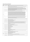
The sample code described in this application note has been checked under the conditions listed in the table below.
Table 2-1 Operation Check Conditions
Item
Microcontroller used
Description
RL78/G12 (R5F1026A)
Operating frequency
Main clock (OSC1): 20 MHz
Operating voltage
3.0 V (Operation is possible within the range of voltage from 2.7 V to 3.0 V.)
Integrated development
CubeSuite+ V2.00.00
environment (CubeSuite+)
C compiler (CubeSuite+)
CA78K0 4.00.00.09
Integrated development
e2studio V3.0.0.22
environment (e2studio)
C compiler (e2studio)
KPIT GNURL78-ELF Toolchain V14.01
Integrated development
IAR Embedded Workbench for Renesas RL78 V1.40.1
environment (IAR)
C compiler (IAR)
3.
IAR C/C++ Compiler for Renesas RL78 V1.40
System Overview
The system consists of a transmitter (subsequently referred to as the simple RL78/G12 transmitter) using the
RL78/G12 target board (QB-R5F1026A-TB), a visible light beacon system reception module (separately sold), and a PC.
The sample program covered in this application note handles the sending of visible light beacon signals from the simple
RL78/G12 transmitter, and the received signals can be checked through a GUI on the PC.
Visible light beacon system reception module
VL-100-USB-3R
(manufactured by NAITO DENSEI MACHIDA MFG. CO. LTD.)
00010001
Connected through USB
Simple RL78/G12 transmitter
Windows PC
ID
Figure 3-1 System Overview
R20AN0321EJ0100 Rev.1.00
Aug 06, 2014
2
RL78/G12
4.
Visible Light Beacon Transmission Program
Characteristics of the Visible Light Beacon System
This section describes the format used in the visible light communications. For details, see the specifications of the
visible light beacon system as defined in Japan Electronics and Information Technology Industries Association (JEITA)
standard CP-1223.
Data rate: 4.8[Kb/s]
Method of transmission: I-4PPM (inverted 4-slot pulse-position modulation)
00
Data (LSB First)
I-4PPM signal
01
10
11
1 0 0 0 0 1 0 0 0 0 1 0 0 0 0 1
Bright
Dark
Preamble (PRE)
Each slot takes up 0.104 ms
(i.e. slots are sent at 9.6 kHz).
Frame configuration:
SOF
Payload
(Start of Frame)
4.1
EOF
(End of Frame)
PRE
F-TYPE
ID/DATA
CRC-16
(6 bits)
(8 bits)
(128 bits)
(16 bits)
Preamble (PRE)
The PRE field defines the starting position of a frame and is not 4-PPM encoded. It consists of three ones followed by
nine zeros (12-slot symbol: 111 000 000 000).
4.2
Frame Type (F-TYPE)
The frame type field holds an 8-bit code that indicates the type of payload. The value is 0x00 in the sample program,
since this indicates a payload for use in testing and development.
4.3
ID/DATA
The length of the ID/DATA field is 128 bits and may be used to hold an ID code and data, or any desired data.
4.4
CRC Field
The CRC field is 16 bits long and is used on the receiving side to determine whether reception of the frame was
successful. The CRC field holds the result calculated by the following generating polynomial.
X16+X15+X2+1
R20AN0321EJ0100 Rev.1.00
Aug 06, 2014
3
RL78/G12
5.
Visible Light Beacon Transmission Program
Description of the Transmitter Board
The simple RL78/G12 transmitter mainly consists of an RL78/G12 target board (QB-R5F1026A-TB) manufactured by
Renesas Electronics Cooperation, with a button-battery holder, switch, and super-bright LED added to the universal
version of the target board. Figure 5-1 is the hardware configuration of the simple transmitter board.
LED1
Super-bright LED
LED2
SW2 for the power supply
SW1 for switching the
ID/DATA
Figure 5-1 RL78/G12 Simple Transmitter
5.1
List of Pins to be Used
Table 5-1 Pins to be Used and their Functions
Pin Name
Input/Output
Description
P10
Output
Control pin for the LED used in visible light communications
P13
Output
Control pin for an indicator LED (LED1)
P14
Output
Control pin for an indicator LED (LED2)
X1
Input
Pin for connection to the 20-MHz resonator
X2
Input
Pin for connection to the 20-MHz resonator
P137
Input
Input for SW1 used to switch the ID/DATA field
5.2
Operation Procedure
5.2.1
Connection to Power Source
Setting the CR-2032 and turning on the power switch enables the visible light beacon system to transmit the signals
through the super-bright LED.
5.2.2
Switching of IDs
Pressing SW1 enables switching of the transmitted ID/DATA field.
Table 5-2 Transmitted ID/DATA Values
Number of Times SW1 is Pressed
F-Type
IDs
0
0
"Renesas.Renesas."
1
0
2
0
3
0
LED1
LED2
On
On
"0356853N1393715E"
Off
On
"ABCDEFGHIJKLMNOP"
On
Off
"VisibleLightComm"
Off
Off
Further pressing of the switch causes the sequence to be repeated.
R20AN0321EJ0100 Rev.1.00
Aug 06, 2014
4
RL78/G12
5.3
Visible Light Beacon Transmission Program
Description of the Components
Table 0-1 List of Components to be Used
Name
Button-battery holder
5.4
Manufacturer
Type Number
COMFORTABLE ELECTRONIC
CH74-2032LF
SW2 for power source
SWITRONIC
SS12D01G4
Super-bright LED
Avago Technologies
HLMP-EL1A-Z1KDV
Fixed resistor of 62
Circuit Diagram
The circuit diagram implemented on the universal RL78/G12 target board is shown below.
Figure 5-2 Circuit Diagram
R20AN0321EJ0100 Rev.1.00
Aug 06, 2014
5
RL78/G12
6.
6.1
Visible Light Beacon Transmission Program
Description of the Software
Outline of the Software Processing
The sample program covered in this application note switches the transmitted ID/DATA field in response to SW1 being
pressed. It also uses an interval timer interrupt that is generated every 104 sec to turn the LED on and off with timing in
accord with the standard for visible light communications.
Figure 6-1 is a schematic view of the system.
Switch-bounce
elimination block
SW
VLC modulation block
RL78/G12
HW
Figure 6-1 Schematic View of the System
6.2
List of Option Byte Settings
Table 6-1 summarizes the settings of the option bytes.
Table 6-1 Option Byte Settings
Address
6.3
Value
Description
000C0H/010C0H
11100000B
Disables the watchdog timer (counting stops after release from the reset state).
000C1H/010C1H
10000001B
LVD OFF
000C2H/010C2H
11100000B
HS mode, HOCO: 24 MHz
000C3H/010C3H
10000100B
Enables the on-chip debugger.
List of Functions
Function Name
Outline
File Name
main
Eliminates switch bounce in the signal from SW1.
main.c
CPU_Init
Initializes the clock pulse generator.
main.c
TIMER_Init
Initializes the timers.
main.c
PORT_Init
Sets port pins.
main.c
VLC_Timer
Handler for timer interrupts (104 sec).
main.c
VLC_InitFrame
Generates the visible light frame for transmission.
vlc.c
VLC_GetPulse
Acquires information on the state of the LED (i.e. whether it is on or off).
vlc.c
VLC_PulseUpdate
Updates the LED state information (i.e. determines whether it is to be
vlc.c
switched on or off).
VLC_Encode4ppm
Handles 4-PPM encoding.
vlc.c
VLC_GetCrc
Generates CRC code.
vlc.c
R20AN0321EJ0100 Rev.1.00
Aug 06, 2014
6
RL78/G12
6.4
Visible Light Beacon Transmission Program
Function Specifications
This section describes the specifications for the functions that are used in the sample program.
[Function Name] main
Synopsis
Eliminates switch bounce in the signal from SW1.
Declaration
void main(void)
Explanation
This function calls the initialization function of the hardware and its main loop handles elimination of
switch bounce. It also sets a flag to indicate the ID/DATA field currently being transmitted and switches
the indicator LEDs on detection of the falling edge of SW1.
Arguments
None
Return value
None
[Function Name] CPU_Init
Synopsis
Initializes the clock pulse generator.
Declaration
void CPU_Init(void)
Explanation
This function sets the clock operating mode to the X1 oscillation mode, sets the high-speed system
clock (fMX) as the system clock, enables operation of the X1 oscillation circuit, and disables the highspeed on-chip oscillator clock.
Arguments
None
Return value
None
[Function Name] TIMER_Init
Synopsis
Initializes the timers.
Declaration
void TIMER_Init(void)
Explanation
This function activates the timer array unit to measure intervals of 104.15 us and 10 ms.
Arguments
None
Return value
None
[Function Name] PORT_Init
Synopsis
Sets port pins.
Declaration
void PORT_Init(void)
Explanation
This function makes the port register (Px), port mode register (PMx), port mode control register (PMCx),
pull-up resistor option register (PUx), port input mode register (PIMx), port output mode register (POMx),
and A/D port configuration register (ADPC) settings for the respective pins.
Arguments
None
Return value
None
[Function Name] VLC_Timer
Synopsis
Handler for timer interrupts (104 sec).
Declaration
void VLC_Timer(void)
Explanation
This function is the handler for the 104-us interval interrupts and determines whether the LED for visible
light transmission is to be turned on or off, or to be left in its current state, as each 104-us interval
elapses. When the ID/DATA field is to be switched in response to SW1 being pressed, the frame
updating function (VLC_InitFrame) is also called from within the interrupt handler.
Arguments
None
Return value
None
R20AN0321EJ0100 Rev.1.00
Aug 06, 2014
7
RL78/G12
Visible Light Beacon Transmission Program
[Function Name] VLC_InitFrame
Synopsis
Generates the visible light frame for transmission.
Declaration
void VLC_InitFrame( unsigned char frame_type, unsigned char *payload )
Explanation
This function generates the visible light frame for transmission in an internal buffer.
Arguments
frame_type : Frame type
Return value
None
Payload: 16-byte ID data
[Function Name] VLC_GetPulse
Synopsis
Acquires information on the state of the LED (i.e. whether it is on or off).
Declaration
unsigned char VLC_GetPulse(void)
Explanation
This function acquires information on the state of the LED (i.e. whether it is on or off).
Arguments
None
Return value
0: LED is on.
1: LED is off.
[Function Name] VLC_PulseUpdate
Synopsis
Updates the LED state information (i.e. determines whether it is to be switched on or off).
Declaration
unsigned char VLC_PulseUpdate( void )
Explanation
This function updates the LED state information (i.e. determines whether it is to be switched on or off) in
Arguments
None
Return value
0: In the midst of frame transmission 1: At the end of the frame
accordance with the frame being transmitted.
[Function Name] VLC_Encode4ppm
Synopsis
Handles 4-PPM encoding.
Declaration
unsigned short VLC_Encode4ppm( unsigned char data )
Explanation
This function converts 8-bit data to 4-PPM data (taking up 16 slots).
Arguments
8-bit data
Return value
16 slots of 4-PPM data
[Function Name] VLC_GetCrc
Synopsis
Generates CRC code.
Declaration
unsigned short VLC_GetCrc( unsigned char *buff, int size )
Explanation
This function generates the CRC code.
Arguments
buff: Address where the buffer for storing the CRC code starts.
Return value
CRC code
Size: Buffer size
R20AN0321EJ0100 Rev.1.00
Aug 06, 2014
8
RL78/G12
6.5
Visible Light Beacon Transmission Program
List of Constants
Constant
Setting
vlc_payload[4][16]
"Renesas.Renesas."
Description
ID/DATA fields for transmission
"0356853N1393715E"
"ABCDEFGHIJKLMNOP"
"VisibleLightComm"
led_table[4][2]
{LED_ON,LED_ON}
Information on the states of the indicator LEDs
{LED_OFF,LED_ON}
(sequence of whether they are to be on or off)
{LED_ON,LED_OFF}
{LED_OFF,LED_OFF}
crc16_table[256]
See the source code.
Table information for generating CRC16
(X16+X15+X2+1)
bitrev_table[256]
See the source code.
Table for acquiring 1-byte of bit-inverted data
vlc_4ppm_table[4]
{0x08U, 0x02U, 0x04U, 0x01U}
Table of 4-PPM slot-level sequences
6.6
List of Variables
Table 6-2 lists the global variables that are used in this sample program.
Table 6-2 Global Variables
Type
chattering
Variable Name
chat
Contents
SW information from sampling three times at 10-ms
Function Used
main
intervals
unsigned char
id_change
Flag to indicate timing of ID/DATA switching
main
VLC_Timer
unsigned char
id_sel
Index of ID/DATA field currently being transmitted
main
(0 to 3)
VLC_Timer
unsigned char
sw1
SW1 information after bounce is eliminated
main
unsigned char
tx_buff[]
Frame of data for visible light transmission
VLC_InitFrame
VLC_PulseUpdate
unsigned char
tx_buff_ptr
Index information on the buffer holding the frame of
VLC_PulseUpdate
data for visible light transmission
int
state
Current internal state
VLC_PulseUpdate
int
next_state
Next internal state to be entered
VLC_PulseUpdate
unsigned short
slot_pattern
Slot data for 4-PPM symbols
VLC_PulseUpdate
unsigned short
slot_num
The number of slots that have been updated
VLC_PulseUpdate
unsigned char
vlc_pulse
Information on the state of the LED (i.e. whether it is
VLC_GetPulse
on or off)
VLC_PulseUpdate
R20AN0321EJ0100 Rev.1.00
Aug 06, 2014
9
RL78/G12
6.7
Visible Light Beacon Transmission Program
Flowcharts
Figure 6-2 shows the flow of the main routine of the sample program.
main
DI()
Set the CPU clock.
Set the pins.
Set the timer.
Initial registration of the
ID/DATA field for visible
light transmission
EI()
HALT()
Has the flag
for the 10-ms timer
been set?
No
Yes
Elimination of bounce.
Has the
rising edge been
detected?
No
Yes
Updating of the ID/DATA
number
The flag to indicate switching
of the ID/DATA is set.
The indicator LEDs are
switched on or off.
Figure 6-2 Flow of Main
R20AN0321EJ0100 Rev.1.00
Aug 06, 2014
10
RL78/G12
6.7.1
Visible Light Beacon Transmission Program
Timer Interrupt Function
Figure 6-3 shows the flow of the timer interrupt function.
VLC_Timer
Acquire information on the
LED state (on or off)
Is LED on?
Yes
No
LED is off.
LED is on.
Update the LED state
information (whether to be
switched on or off)
End of frame?
No
Yes
Has the flag
to indicate switching
of the ID/DATA field
been set?
No
Yes
The ID/DATA field for visible
light transmission is changed.
RETI
Figure 0-1 Timer Interrupt Function
R20AN0321EJ0100 Rev.1.00
Aug 06, 2014
11
RL78/G12
6.7.2
Visible Light Beacon Transmission Program
Function to Update the LED State Information (Whether to be Switched On or Off)
Figure 6-4 shows the flow of processing by the function to update the LED state information (i.e. whether it is to be
switched on or off).
VLC_PulseUpdate
loop = 1
frame_end = 0
Loop = 1?
Yes
No
state
SET_PREAMBLE
SET_FRAME
CHECK_FRAME
tx_buff_ptr = 0
4-PPM encoding
tx_buff_ptr++
slot_pattern =
0b111000000000
slot_pattern =
4-PPM encoded data
Has transmission
of all frames been
completed?
state =
OUTPUT_4PPM
state =
OUTPUT_4PPM
frame_end = 1
next_state =
SET_FRAME
next_state =
CHECK_FRAME
next_state =
SET_PREAMBLE
OUTPUT_4PPM
The LED state information
(whether to be switched on or off)
is acquired from slot_pattern.
loop = 0
No
Yes
Have all slots
been output?
No
Yes
next_state =
SET_FRAME
state = next_state
Return(frame_end)
Figure 6-4 Updating of LED State Information (On or Off)
7.
Sample Program
The sample program is available on the Renesas Electronics Website.
8.
Documents for Reference
RL78/G12 User's Manual: Hardware (R01UH0200E)
RL78 Family User's Manual: Software (R01US0015E)
(The latest versions of the documents are available on the Renesas Electronics Website.)
Technical Updates/Technical Brochures
(The latest versions of the documents are available on the Renesas Electronics Website.)
Website and Support
Renesas Electronics Website
http://www.renesas.com/index.jsp
Inquiries
http://www.renesas.com/contact/
R20AN0321EJ0100 Rev.1.00
Aug 06, 2014
12
Revision Record
Rev.
Date
1.00
Aug 06, 2014
RL78/G12 Visible Light Beacon Transmission Program
Page
—
Description
Summary
First edition issued
All trademarks and registered trademarks are the property of their respective owners.
A-1
General Precautions in the Handling of MPU/MCU Products
The following usage notes are applicable to all MPU/MCU products from Renesas. For detailed usage notes on the
products covered by this document, refer to the relevant sections of the document as well as any technical updates that
have been issued for the products.
1. Handling of Unused Pins
Handle unused pins in accordance with the directions given under Handling of Unused Pins in the
manual.
⎯ The input pins of CMOS products are generally in the high-impedance state. In operation with an
unused pin in the open-circuit state, extra electromagnetic noise is induced in the vicinity of LSI, an
associated shoot-through current flows internally, and malfunctions occur due to the false
recognition of the pin state as an input signal become possible. Unused pins should be handled as
described under Handling of Unused Pins in the manual.
2. Processing at Power-on
The state of the product is undefined at the moment when power is supplied.
⎯ The states of internal circuits in the LSI are indeterminate and the states of register settings and
pins are undefined at the moment when power is supplied.
In a finished product where the reset signal is applied to the external reset pin, the states of pins
are not guaranteed from the moment when power is supplied until the reset process is completed.
In a similar way, the states of pins in a product that is reset by an on-chip power-on reset function
are not guaranteed from the moment when power is supplied until the power reaches the level at
which resetting has been specified.
3. Prohibition of Access to Reserved Addresses
Access to reserved addresses is prohibited.
⎯ The reserved addresses are provided for the possible future expansion of functions. Do not access
these addresses; the correct operation of LSI is not guaranteed if they are accessed.
4. Clock Signals
After applying a reset, only release the reset line after the operating clock signal has become stable.
When switching the clock signal during program execution, wait until the target clock signal has
stabilized.
⎯ When the clock signal is generated with an external resonator (or from an external oscillator)
during a reset, ensure that the reset line is only released after full stabilization of the clock signal.
Moreover, when switching to a clock signal produced with an external resonator (or by an external
oscillator) while program execution is in progress, wait until the target clock signal is stable.
5. Differences between Products
Before changing from one product to another, i.e. to a product with a different part number, confirm
that the change will not lead to problems.
⎯ The characteristics of an MPU or MCU in the same group but having a different part number may
differ in terms of the internal memory capacity, layout pattern, and other factors, which can affect
the ranges of electrical characteristics, such as characteristic values, operating margins, immunity
to noise, and amount of radiated noise. When changing to a product with a different part number,
implement a system-evaluation test for the given product.
Notice
1.
Descriptions of circuits, software and other related information in this document are provided only to illustrate the operation of semiconductor products and application examples. You are fully responsible for
the incorporation of these circuits, software, and information in the design of your equipment. Renesas Electronics assumes no responsibility for any losses incurred by you or third parties arising from the
use of these circuits, software, or information.
2.
Renesas Electronics has used reasonable care in preparing the information included in this document, but Renesas Electronics does not warrant that such information is error free. Renesas Electronics
3.
Renesas Electronics does not assume any liability for infringement of patents, copyrights, or other intellectual property rights of third parties by or arising from the use of Renesas Electronics products or
assumes no liability whatsoever for any damages incurred by you resulting from errors in or omissions from the information included herein.
technical information described in this document. No license, express, implied or otherwise, is granted hereby under any patents, copyrights or other intellectual property rights of Renesas Electronics or
others.
4.
You should not alter, modify, copy, or otherwise misappropriate any Renesas Electronics product, whether in whole or in part. Renesas Electronics assumes no responsibility for any losses incurred by you or
5.
Renesas Electronics products are classified according to the following two quality grades: "Standard" and "High Quality". The recommended applications for each Renesas Electronics product depends on
third parties arising from such alteration, modification, copy or otherwise misappropriation of Renesas Electronics product.
the product's quality grade, as indicated below.
"Standard": Computers; office equipment; communications equipment; test and measurement equipment; audio and visual equipment; home electronic appliances; machine tools; personal electronic
equipment; and industrial robots etc.
"High Quality": Transportation equipment (automobiles, trains, ships, etc.); traffic control systems; anti-disaster systems; anti-crime systems; and safety equipment etc.
Renesas Electronics products are neither intended nor authorized for use in products or systems that may pose a direct threat to human life or bodily injury (artificial life support devices or systems, surgical
implantations etc.), or may cause serious property damages (nuclear reactor control systems, military equipment etc.). You must check the quality grade of each Renesas Electronics product before using it
in a particular application. You may not use any Renesas Electronics product for any application for which it is not intended. Renesas Electronics shall not be in any way liable for any damages or losses
incurred by you or third parties arising from the use of any Renesas Electronics product for which the product is not intended by Renesas Electronics.
6.
You should use the Renesas Electronics products described in this document within the range specified by Renesas Electronics, especially with respect to the maximum rating, operating supply voltage
range, movement power voltage range, heat radiation characteristics, installation and other product characteristics. Renesas Electronics shall have no liability for malfunctions or damages arising out of the
use of Renesas Electronics products beyond such specified ranges.
7.
Although Renesas Electronics endeavors to improve the quality and reliability of its products, semiconductor products have specific characteristics such as the occurrence of failure at a certain rate and
malfunctions under certain use conditions. Further, Renesas Electronics products are not subject to radiation resistance design. Please be sure to implement safety measures to guard them against the
possibility of physical injury, and injury or damage caused by fire in the event of the failure of a Renesas Electronics product, such as safety design for hardware and software including but not limited to
redundancy, fire control and malfunction prevention, appropriate treatment for aging degradation or any other appropriate measures. Because the evaluation of microcomputer software alone is very difficult,
please evaluate the safety of the final products or systems manufactured by you.
8.
Please contact a Renesas Electronics sales office for details as to environmental matters such as the environmental compatibility of each Renesas Electronics product. Please use Renesas Electronics
products in compliance with all applicable laws and regulations that regulate the inclusion or use of controlled substances, including without limitation, the EU RoHS Directive. Renesas Electronics assumes
no liability for damages or losses occurring as a result of your noncompliance with applicable laws and regulations.
9.
Renesas Electronics products and technology may not be used for or incorporated into any products or systems whose manufacture, use, or sale is prohibited under any applicable domestic or foreign laws or
regulations. You should not use Renesas Electronics products or technology described in this document for any purpose relating to military applications or use by the military, including but not limited to the
development of weapons of mass destruction. When exporting the Renesas Electronics products or technology described in this document, you should comply with the applicable export control laws and
regulations and follow the procedures required by such laws and regulations.
10. It is the responsibility of the buyer or distributor of Renesas Electronics products, who distributes, disposes of, or otherwise places the product with a third party, to notify such third party in advance of the
contents and conditions set forth in this document, Renesas Electronics assumes no responsibility for any losses incurred by you or third parties as a result of unauthorized use of Renesas Electronics
products.
11. This document may not be reproduced or duplicated in any form, in whole or in part, without prior written consent of Renesas Electronics.
12. Please contact a Renesas Electronics sales office if you have any questions regarding the information contained in this document or Renesas Electronics products, or if you have any other inquiries.
(Note 1)
"Renesas Electronics" as used in this document means Renesas Electronics Corporation and also includes its majority-owned subsidiaries.
(Note 2)
"Renesas Electronics product(s)" means any product developed or manufactured by or for Renesas Electronics.
http://www.renesas.com
SALES OFFICES
Refer to "http://www.renesas.com/" for the latest and detailed information.
Renesas Electronics America Inc.
2801 Scott Boulevard Santa Clara, CA 95050-2549, U.S.A.
Tel: +1-408-588-6000, Fax: +1-408-588-6130
Renesas Electronics Canada Limited
1101 Nicholson Road, Newmarket, Ontario L3Y 9C3, Canada
Tel: +1-905-898-5441, Fax: +1-905-898-3220
Renesas Electronics Europe Limited
Dukes Meadow, Millboard Road, Bourne End, Buckinghamshire, SL8 5FH, U.K
Tel: +44-1628-585-100, Fax: +44-1628-585-900
Renesas Electronics Europe GmbH
Arcadiastrasse 10, 40472 Düsseldorf, Germany
Tel: +49-211-6503-0, Fax: +49-211-6503-1327
Renesas Electronics (China) Co., Ltd.
Room 1709, Quantum Plaza, No.27 ZhiChunLu Haidian District, Beijing 100191, P.R.China
Tel: +86-10-8235-1155, Fax: +86-10-8235-7679
Renesas Electronics (Shanghai) Co., Ltd.
Unit 301, Tower A, Central Towers, 555 Langao Road, Putuo District, Shanghai, P. R. China 200333
Tel: +86-21-2226-0888, Fax: +86-21-2226-0999
Renesas Electronics Hong Kong Limited
Unit 1601-1613, 16/F., Tower 2, Grand Century Place, 193 Prince Edward Road West, Mongkok, Kowloon, Hong Kong
Tel: +852-2265-6688, Fax: +852 2886-9022/9044
Renesas Electronics Taiwan Co., Ltd.
13F, No. 363, Fu Shing North Road, Taipei 10543, Taiwan
Tel: +886-2-8175-9600, Fax: +886 2-8175-9670
Renesas Electronics Singapore Pte. Ltd.
80 Bendemeer Road, Unit #06-02 Hyflux Innovation Centre, Singapore 339949
Tel: +65-6213-0200, Fax: +65-6213-0300
Renesas Electronics Malaysia Sdn.Bhd.
Unit 906, Block B, Menara Amcorp, Amcorp Trade Centre, No. 18, Jln Persiaran Barat, 46050 Petaling Jaya, Selangor Darul Ehsan, Malaysia
Tel: +60-3-7955-9390, Fax: +60-3-7955-9510
Renesas Electronics Korea Co., Ltd.
12F., 234 Teheran-ro, Gangnam-Ku, Seoul, 135-920, Korea
Tel: +82-2-558-3737, Fax: +82-2-558-5141
© 2014 Renesas Electronics Corporation. All rights reserved.
Colophon 4.0