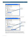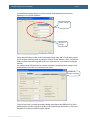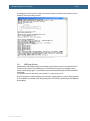
1
LPC2478 Developer’s Kit - User‟s Guide Copyright 2011 © Embedded Artists AB LPC2478 Developer’s Kit User’s Guide Get Up-and-Running Quickly and Start Developing Your Applications On Day 1! EA2-USG-0801 Rev I LPC2478 Developer’s Kit - User’s Guide Page 2 Embedded Artists AB Davidshallsgatan 16 211 45 Malmö Sweden [email protected] http://www.EmbeddedArtists.com Copyright 2005-2011 © Embedded Artists AB. All rights reserved. No part of this publication may be reproduced, transmitted, transcribed, stored in a retrieval system, or translated into any language or computer language, in any form or by any means, electronic, mechanical, magnetic, optical, chemical, manual or otherwise, without the prior written permission of Embedded Artists AB. Disclaimer Embedded Artists AB makes no representation or warranties with respect to the contents hereof and specifically disclaim any implied warranties or merchantability or fitness for any particular purpose. Information in this publication is subject to change without notice and does not represent a commitment on the part of Embedded Artists AB. Feedback We appreciate any feedback you may have for improvements on this document. Please send your comments to [email protected]. Trademarks All brand and product names mentioned herein are trademarks, services marks, registered trademarks, or registered service marks of their respective owners and should be treated as such. Copyright 2011 © Embedded Artists AB LPC2478 Developer’s Kit - User’s Guide Page 3 Table of Contents 1 Document Revision History 5 2 Introduction 6 2.1 Features 6 2.2 ESD Precaution 7 2.3 General Handling Care 7 2.4 Code Read Protection 8 2.5 CE Assessment 8 2.6 Other Products from Embedded Artists 8 2.6.1 Design and Production Services 8 2.6.2 OEM / Education / QuickStart Boards and Kits 9 3 LPC2478 OEM Board Design 3.1 LPC2478 OEM Board Schematics 10 3.1.1 CPU 10 3.1.2 Powering 10 3.1.3 Analog Inputs/Outputs 10 3.1.4 Ethernet Interface 10 3.1.5 External Memories 11 3.1.6 External Memory Interface 11 3.1.7 Reset Generation 11 3.1.8 I2C E2PROM 11 3.1.9 Expansion Connectors 12 3.2 Memory Layout 12 3.3 Usage of CPU Pins 12 3.4 LPC2478 OEM Board Mechanical Dimensions and Connector 13 3.5 Known Limitation of LPC2478 OEM Board 14 3.5.1 Ver 1.0 – SDRAM Clock Frequency 14 3.5.2 Ver 1.0 – Ethernet Clock 14 3.5.3 NAND FLASH Bad Block 14 3.5.4 Brand of Memory Chips 15 4 QVGA Base Board Design 16 4.1 Usage of CPU Pins 16 4.2 Known Limitation of QVGA Base Board 19 4.2.1 4.3 Version 1.0/1.1 – SD/MMC Interface Pullups Jumpers 19 20 4.3.1 Default Jumper Positions 21 4.3.2 Illegal Jumper Combinations 21 4.4 4.4.1 4.5 Connectors Mictor-38 ETM Connector Important Components 5 Getting Started Copyright 2011 © Embedded Artists AB 10 22 22 23 24 LPC2478 Developer’s Kit - User’s Guide Page 4 5.1 5.1.1 Demo Applications Custom Slideshow Demo Application #3 24 5.2 Initial Setup and Powering 26 5.3 Getting Started with uClinux 28 5.3.1 Basic Requirements 28 5.3.2 LAN/Ethernet Setup 28 5.4 5.4.1 FTDI USB Driver Installation USB Driver Behavior 6 Further Information Copyright 2011 © Embedded Artists AB 24 30 33 34 LPC2478 Developer’s Kit - User’s Guide Page 5 1 Document Revision History Revision Date Description A-G 2007-2010 Earlier versions of document. H 2010-12-10 Updated manual according to new template. Removed schematics from document. Added known issue with newer SD/MMC memory cards (requiring pull-up resistors). I 2011-12-19 Added note about CE marking. Copyright 2011 © Embedded Artists AB LPC2478 Developer’s Kit - User’s Guide Page 6 2 Introduction Thank you for buying Embedded Artists‟ LPC2478 Developer’s Kit based on NXP‟s ARM7TDMI-S LPC2478 microcontroller. This document is a User‟s Guide that describes the LPC2478 OEM Board (both 16- and 32-bit data bus versions) and the QVGA Base Board hardware design. It is the User‟s Manual for both the LPC2478 Developer’s Kit as well as for just the LPC2478 OEM Board. There is a separate document describing program development for the LPC2xxx series in general with Embedded Artists QuickStart Build Environment. 2.1 Features Embedded Artists‟ LPC2478 OEM Board with NXP‟s ARM7TDMI-S LPC2478 microcontroller lets you get up-and-running quickly. The small form factor OEM board offers many unique features that ease your learning curve and program development. The board has also been designed for OEM applications with volume discount available. NXP's ARM7TDMI LPC2478 microcontroller in BGA package, with 512 KByte program FLASH and 96 KByte SRAM External FLASH memories: 128 MB NAND FLASH and 4 MB NOR FLASH External data memory: 32 MB SDRAM (32-bit or 16-bit databus width) 12.0000 MHz crystal for maximum execution speed and standard serial bit rates, including CAN and USB requirements 32.768kHz RTC crystal 100/10M Ethernet PHY/interface based on National DP83848 256 Kbit I2C E2PROM for storing non-volatile parameters Buffered 16- or 32-bit data bus for external expansion 200 pos expansion connector (SODIMM-200 format, 0.6mm pitch) All LPC2478 pins available (except a few used for Ethernet-PHY interface) +3.3V only powering Onboard reset generation Compact SODIMM format: 66 x 48 mm Six layer PCB design for best noise immunity There is an accompanying QVGA Base Board that can be used for initial prototyping work. The features of the board are: 3.2 inch QVGA TFT color LCD with touch screen (4-wire version) Copyright 2011 © Embedded Artists AB 18-bit RGB interface to display Connectors 200 pos, 0.6mm pitch SODIMM connector for LPC2478 OEM Board Expansion connector with all LCD controller signals, for custom displays Expansion connector with all cpu signals Ethernet connector (RJ45) LPC2478 Developer’s Kit - User’s Guide CAN interface & connector MMC/SD interface & connector JTAG connector Pads for ETM connector Interfaces USB OTG interface & connector USB host interface & connector Full modem RS232 on UART #1 (cannot be used on 32-bit databus cpu boards, but RxD2/TxD2 can alternatively be connected to the RS232 interface) Dual CAN interface & connector IrDA transceiver interface Power 2.2 Page 7 Power supply, either via USB or external 9-15V DC 0.3F capacitor backup power for RTC and LED on ALARM output on LPC2478 Other 5-key joystick 3-axis accelerometer 5 push-button keys (four via I2C and one on P2.10) 9 LEDs (8 via I2C and one on P2.10) Analog input USB-to-serial bridge on UART #0 (FT232R) and ISP functionality Reset push-button and LED Speaker output on DAC output from LPC2478 250x150 mm in size ESD Precaution Please note that the LPC2478 OEM Board and QVGA Base Board come without any case/box and all components are exposed for finger touches – and therefore extra attention must be paid to ESD (electrostatic discharge) precaution. Make it a habit always to first touch the metal surface of one of the USB or Ethernet connectors for a few seconds with both hands before touching any other parts of the boards. That way, you will have the same potential as the board and therefore minimize the risk for ESD. Never touch directly on the LPC2478 OEM Board and in general as little as possible on the QVGA Base Board. The push-buttons on the QVGA Base Board have grounded shields to minimize the effect of ESD. Note that Embedded Artists does not replace boards that have been damaged by ESD. 2.3 General Handling Care Handle the LPC2478 OEM Board and QVGA Base Board with care. The boards are not mounted in a protective case/box and are not designed for rough physical handling. Connectors can ware out after Copyright 2011 © Embedded Artists AB LPC2478 Developer’s Kit - User’s Guide Page 8 excessive use. The QVGA Base Board is designed for prototyping use, and not for integration into an end-product. Do not exercise excessive pressure on the LCD glass area. That will damage the display. Also, do not apply pressure on the flex cables connecting the LCD/touch screen. These are relatively sensitive and can be damaged if too much pressure is applied to them. Note that Embedded Artists does not replace boards where the LCD has been improperly handled. 2.4 Code Read Protection The LPC2478 has a Code Read Protection function (specifically CRP3) that, if enabled, will make the LPC2478 impossible to reprogram (unless the user program has implemented such functionality). Note that Embedded Artists does not replace LPC2478 OEM boards where the LPC2478 has CRP3 enabled. It’s the user’s responsibility to not invoke this mode by accident. 2.5 CE Assessment The LPC2478 Developers Kit (consisting of the LPC2478 OEM Board and QVGA Base Board) is CE marked. See separate CE Declaration of Conformity document. The LPC2478 Developers Kit is a class A product. In a domestic environment this product may cause radio interference in which case the user may be required to take adequate measures. EMC emission test has been performed on the LPC2478 Developers Kit. Standard interfaces like Ethernet, USB, serial have been in use. General expansion connectors where internal signals are made available (for example processor pins) have been left unconnected. Connecting other devices to the product via the general expansion connectors may alter EMC emission. It is the user‟s responsibility to make sure EMC emission limits are not exceeded when connecting other devices to the general expansion connectors of the LPC2478 Developers Kit. Due to the nature of the LPC2478 Developers Kit – an evaluation board not for integration into an endproduct – fast transient immunity tests and conducted radio-frequency immunity tests have not been executed. Externally connected cables are assumed to be less than 3 meters. The general expansion connectors where internal signals are made available do not have any other ESD protection than from the chip themselves. Observe ESD precaution. Note that the LPC2478 OEM board is classified as a component and is hence not CE marked separately. It can perform different functions in different integrations and it does not have a direct function. It is therefore not in the scope of the CE Directive. An end product, where an OEM Board is integration into, is however very likely to need CE marking. 2.6 Other Products from Embedded Artists Embedded Artists have a broad range of LPC1000/2000/3000/4000 based boards that are very low cost and developed for prototyping / development as well as for OEM applications. Modifications for OEM applications can be done easily, even for modest production volumes. Contact Embedded Artists for further information about design and production services. 2.6.1 Design and Production Services Embedded Artists provide design services for custom designs, either completely new or modification to existing boards. Specific peripherals and I/O can be added easily to different designs, for example, communication interfaces, specific analog or digital I/O, and power supplies. Embedded Artists has a broad, and long, experience in designing industrial electronics in general and with NXP‟s LPC1000/2000/3000/4000 microcontroller families in specific. Our competence also includes wireless and wired communication for embedded systems. For example IEEE802.11b/g (WLAN), Bluetooth™, ZigBee™, ISM RF, Ethernet, CAN, RS485, and Fieldbuses. Copyright 2011 © Embedded Artists AB LPC2478 Developer’s Kit - User’s Guide 2.6.2 Page 9 OEM / Education / QuickStart Boards and Kits Visit Embedded Artists‟ home page, www.EmbeddedArtists.com, for information about other OEM / Education / QuickStart boards / kits or contact your local distributor. Copyright 2011 © Embedded Artists AB LPC2478 Developer’s Kit - User’s Guide Page 10 3 LPC2478 OEM Board Design This chapter contains information about the LPC2478 OEM Board design, both 32-bit and 16-bit databus width. The schematic can be downloaded in pdf from the support page, and is recommended to have printed out while reading this chapter. 3.1 LPC2478 OEM Board Schematics 3.1.1 CPU The core part of the design is the NXP LPC2478 microcontroller. It‟s an ARM7TDMI-S CPU core with a lot of different peripheral units and on-chip memory (512 KByte FLASH and 96 KByte SRAM). There is also an external memory bus interface. Page 2 of the schematic contains the CPU section of the design. The microcontroller crystal frequency is 12.0000 MHz. This frequency has been selected in order to allow high execution speed (the PLL can generate a 72 MHz core clock from this) as well as generating standard clock frequencies for the CAN and USB interfaces. The on-chip UART peripheral includes a fractional baud rate generator that allows standard baud rates to be generated with low frequency error. There is a 32.768 kHz crystal clock for the on-chip real-time clock peripheral unit or RTC for short. The microcontroller can be placed in a very low power mode while the RTC operates and keeps track of time. Power for the RTC (during these low power modes) comes from the VBAT input pin. Power is sourced either from the +3.3V power supply or the external VBAT_IN signal (available on the expansion connector), depending on which one have highest voltage. 3.1.2 Powering There is no internal power supply on the board. The LPC2478 contains an internal DC/DC converter to generate the internal 1.8V power needed by the core. The LPC2478 OEM Board module must be powered by a single, external +3.3V power supply. The supply must be stable and should have at least four 22uF bulk capacitor(s) close to the power pins on the expansion connectors. 3.1.3 Analog Inputs/Outputs The LPC2478 contains analog peripherals that need a reference voltage, which is supplied from the VREF input pin. This reference voltage must be supplied externally can be the VDDA power (which is a filtered +3.3V power supply). The VDDA power is available on the expansion connector under the name V3A. See schematic for details. A filtered version of analog ground is also available under the name VSSA. 3.1.4 Ethernet Interface The LPC2478 have an internal Ethernet MAC peripheral with interface to an external PHY (i.e., the analog interface to an Ethernet interface). Page 2 of the schematic contains the Ethernet PHY. The DP83848 external Ethernet PHY from National is used and interfaces the LPC2478 via the RMII interface. The PHY is driven by an external 50 MHz clock that is also feed to the LPC2478. This is part of the RMII interface specification. The PHY is always enables (can be disabled under program control) but have an external „power down‟ signal that can be used by an external device. There is also an interrupt signal from the PHY that can be used to signal link events (like connect/disconnect of a cable). Neither the power down nor the interrupt signal is used by the LPC2478 OEM Board but the signals are available on the expansion connector. If the signals are not used, just leave them unconnected. Copyright 2011 © Embedded Artists AB LPC2478 Developer’s Kit - User’s Guide 3.1.5 Page 11 External Memories There are three external memory chips connected to the external memory bus interface of the LPC2478. Both 32-bit and 16-bit databus width versions of the board exist. An external NOR FLASH (32 MBit = 4 MByte in size) addressed by CS0 (address range: 0x8000 0000 – 0x80FF FFFF). Accessed via 16-bit databus. An external NAND FLASH (1 GBit = 128 MByte in size) addressed by CS1 (address range: 0x8100 0000 – 0x81FF FFFF). Accessed via 8-bit databus. An external SDRAM (256 MBit = 32 MByte in size) addressed by DYCS0 (address range: 0xA000 0000 – 0xAFFF FFFF). Accessed via 32-bit or 16-bit databus, dependent on board version. The NAND FLASH has an optional busy output that can be used for controlling the erase/program operations with better precision. The signal is available on the expansion connector. If needed the signal can be routed to a suitable (i.e., free) input pin. The busy status of the chip is also available under software control. 3.1.6 External Memory Interface The LPC2478 memory interface is available on the expansion connector. The data bus width is either 16- or 32-bits on the external interface (depending on board version). All signals are buffered. The buffers are disabled unless enabled by external signals. By pulling signal ABUF_EN low, the two buffers for address and control signals are enabled and act as outputs (from the LPC2478 OEM Board). The data bus buffer is controlled by the signal DBUS_EN. By pulling this signal low, the data bus buffer is enabled. The LPC2478 signal OE controls the direction of the data bus buffer. During read operations the buffer acts as an input and during write operations it acts as an output. Note that DBUS_EN must not be pulled low constantly. In that case the buffer will collide with the board‟s internal data bus. DBUS_EN must only be pulled low when an external memory/IO device is accessed. If, for example, CS2 is used to decode and access an external device, connect the signal CS2 directly to DBUS_EN. If more than one chip select signal is used, (logically) AND all chip select signal together before driving the DBUS_EN signal. If the external memory interface is not used, leave ABUS_EN and DBUS_EN unconnected. 3.1.7 Reset Generation The rest generation is handled by a standard voltage supervisor chip, CAT811S from Catalyst Semiconductor. The reset signal will be held active (i.e., low) until the supply voltages, +3.3V, is within margins. The reset duration is typically 200 mS (consult the CAT811S datasheet for exact details). The output reset signal is push/pull output that is converted to an open-collector / open-drain output via the 74LVC1G125 buffer. An external reset source can pull the reset signal low (with an opencollector/open-drain output). The reset generator can be found on page 2 of the schematic. 3.1.8 I2C E2PROM There is also a 256 kbit E2PROM accessible via the I2C interface. The LPC2478 microcontroller has three on-chip I2C communication channels. Channel #0 is used for communicating with the E2PROM. More peripheral units are easily connected to the two-wire I2C bus, just as long as the addresses do not collide. The address of the 256kbit E2PROM is 0xA0. There are 1.5 kohm pull-up resistors (which are always needed on I2C busses) included on the board. The I2C E2PROM can be found on page 2 of the schematic. Copyright 2011 © Embedded Artists AB LPC2478 Developer’s Kit - User’s Guide 3.1.9 Page 12 Expansion Connectors The LPC2478 OEM Board integrated the core part of a typical LPC2478 board design with a reasonable large amount of external memories. Almost all signals of LPC2478 are available on the 200 pos, 0.6mm pitch expansion connector (SODIMM-200 format). 3.2 Memory Layout The external memory controller on the LPC2478 defines eight memory regions, named: CS0, CS1, CS2, CS3, DYCS0, DYCS1, DYCS2, and DYCS3. Of these eight, three memory areas are used by the LPC2478 OEM Board. These are: CS0 (address range: 0x8000 0000 – 0x80FF FFFF) An external NOR FLASH (32 MBit = 4 MByte in size) is addressed. CS1 (address range: 0x8100 0000 – 0x81FF FFFF) An external NAND FLASH (1 GBit = 128 MByte in size) is addressed. DYCS0 (address range: 0xA000 0000 – 0xAFFF FFFF) An external SDRAM (256 MBit = 32 MByte in size) is addressed. These three memory regions cannot be used by external devices. CS2 and DYCS1 are however free for external use via the buffered memory interface. Both address and data busses are buffered. 3.3 Usage of CPU Pins Almost all pins of the LPC2478 are directly available on the expansion connectors. Only in a few cases are pins used for dedicated functionality like Ethernet interface and chip select signals. Such pins are not available on the expansion connector. The table below lists all pins and their possible restrictions. Pin Available on expansion connector P0.0-P0.26 Yes P0.27- P0.28 Yes, but I2C E2PROM connected to these pins. P0.29-P0.31 Yes USBB- Yes P1.0-P1.1, P1.4, P1.8-P1.10, P1.14-P1.17 No, connected to Ethernet PHY P1.2-P1.3, P1.5-P1.7, P1.11-P1.13, P1.18- P1.26P1.31 Yes P2.0-P2.15, P2.19, P2.21-P2.23, P2.25-P2.27 Yes P2.16-P2.17 Yes, but used as RAS/CAS and only available as outputs Copyright 2011 © Embedded Artists AB via a buffer P2.18, P2.20, P2.24 No, used as CLKOUT0/DYCS0/CKE0 for external SDRAM P2.28-P2.29 Yes, but used as DQM0/DQM1 (for external SDRAM) and only available as outputs via a buffer P2.30-P2.31 Yes, but used as DQM2/DQM3 (on 32-bit data bus version) P3.0-P3.15 Yes, but used as data bus and only available via data bus buffer P3.16-P3.31 Yes. On 32-bit data bus versions these pins are used for upper 16 bits of the data bus and are only available via the data bus buffer P4.0-P4.23 Yes, but used as address bus and only available as outputs via buffers P4.24-P4.27 Yes, but used as LPC2478 Developer’s Kit - User’s Guide Page 13 OE/WE/BLS0/BLS1 and only available as outputs via a buffer P4.28-P4.29 Yes P4.30-P4.31 No, used as CS0/CS1 for external NOR/NAND FLASH memories VBAT Yes, via forward diode ALARM Yes VREF Yes. Note that VDDA is VDDA, VSSA connected to +3.3V power supply X1-X2, RTCX1RTCX2 No, directly connected to onboard crystals JTAG signals Yes RESET, RSTOUT Yes The QVGA Base Board illustrates how to typically connect external interfaces (like Ethernet, USB, external memory devices, etc) to the LPC2478 OEM Board. Study this schematic (also found in this document) for details. 3.4 LPC2478 OEM Board Mechanical Dimensions and Connector Figure 1 below contains a drawing of the board that includes mechanical measures. See SODIMM-200 standard for exact measures. 1.8V keying is used (SODIMM-200 boards are either 1.8V or 2.5V keyed). 66 mm This is how the 32-bit databus versions look like 48 mm 1.8V keying of SODIMM board Figure 1 - LPC2478 OEM Board Mechanical Dimensions, 32-bit databus version shown The SODIMM-200 format is a standard and there exist many connectors that are suitable form many different manufactures. The many sources also keep the connector cost very low. Note that the connector should be 1.8V keyed. Copyright 2011 © Embedded Artists AB LPC2478 Developer’s Kit - User’s Guide Page 14 One suitable connector is 0-1473005-4 from Tyco/AMP. Basically any SODIMM, DDR2, 200pos, 1.8V, right angled connector will do. 3.5 Known Limitation of LPC2478 OEM Board 3.5.1 Ver 1.0 – SDRAM Clock Frequency There is one known limitation of the LPC2478 OEM Board. The cpu core clock frequency must not exceed 48 MHz when using the external SDRAM. This limitation only applies to v1.0 boards with 32-bit external databus width. Boards with 16-bit databus can run at full speed. On v1.0 of 16-bit boards there is a small modification on the boards. On all v1.1 boards (16- and 32-bit) this limitation is fixed in the design, i.e., the boards can run at full 72MHz. Normally the internal PLL frequency is set to 288 MHz (the external 12 MHz crystal frequency multiplied by 24). Dividing 288 MHz with 6 gives a core frequency of 48 MHz and dividing with 4 gives 72 MHz. The limitation results in a maximum cpu clock frequency of 48 MHz when using the external SDRAM. If the SDRAM is not used, the cpu core frequency can be up to full specification of the LPC2478. 3.5.2 Ver 1.0 – Ethernet Clock Due to an error in clock routing between the Ethernet PHY and the LPC2478, rev 1.0 boards have been modified slightly. The error is also temperature dependent. Only a small number of ver 1.0 boards have been shipped without this modification and these boards were tested not to have any problems. The picture below illustrates the modification made. The problem is fixed on ver 1.1 boards. 1) Pin 25 of the Ethernet PHY has been lifted and removed. 2) A short wire has been soldered to the 50 MHz oscillator output. 3) The wire is soldered in the other end to the pad of the removed Ethernet PHY pin. Figure 2 - LPC2478 OEM Board Ethernet Clock Modification 3.5.3 NAND FLASH Bad Block The NAND Flash is the K9F1G08U0A from Samsung and contains 1G bit with a spare 32M bit capacity. The chip may include invalid blocks when shipped from factory. A maximum of 20 invalid blocks may exist initially, i.e., 1004-1024 valid blocks. Additional invalid blocks may develop while Copyright 2011 © Embedded Artists AB LPC2478 Developer’s Kit - User’s Guide Page 15 being used. Invalid blocks are defined as blocks that contain one or more bad bits. Do not erase or program factory-marked bad blocks. Refer to technical notes from Samsung for appropriate management of invalid blocks. 3.5.4 Brand of Memory Chips Note that there is no guarantee for a certain brand or version of memory chips; NOR flash, NAND flash and SDRAM. The lifetime of memory chips is limited and availability can also be limited from time to time. Embedded Artists make every effort to mount the original design chip on the board. In case that is impossible a compatible chip will instead be mounted without any prior notice. There can be small programming differences between mounted brands. The application program shall always read the chip id of flash devices to make certain which chip is actually mounted on the board. The support page contains datasheets to the different memory devices and information about mounted devices on different board versions. Copyright 2011 © Embedded Artists AB LPC2478 Developer’s Kit - User’s Guide Page 16 4 QVGA Base Board Design This chapter contains information about the peripherals and general design of the QVGA Base Board and how to set the different jumpers on the board. The schematic can be downloaded in pdf from the support page, and is recommended to have printed out while reading this chapter. The QVGA Base Board contains a number interfaces and connectors to the LPC2478 OEM Board. The design can be viewed as a reference schematic for custom designs around the LPC2478 OEM Board. 4.1 Usage of CPU Pins Almost all pins of the LPC2478 are directly available on the expansion connectors. Only in a few cases are pins used for dedicated functionality like Ethernet interface and chip select signals. Such pins are not available on the expansion connector. The table below lists all pins and their possible restrictions. Pin Usage P0.0 Can be connected to RD1 for CAN channel #1, can also connect to IrDA transceiver P0.1 Can be connected to TD1 for CAN channel #1, can also connect to IrDA transceiver P0.2 Can be connected to USB-to-serial bridge (TxD on UART #0) P0.3 Can be connected to USB-to-serial bridge (RxD on UART #0) P0.4 LCD databit 0, can also be connected to RD2 for CAN channel #2 P0.5 LCD databit 1, can also be connected to TD2 for CAN channel #2 P0.6 LCD databit 8 P0.7 LCD databit 9 P0.8 LCD databit 16 P0.9 LCD databit 17 P0.10 Can be connected to RS232 interface (TxD on UART #2) P0.11 Can be connected to RS232 interface (RxD on UART #2) P0.12 Can be connected to enable USB-host power switch P0.13 Can be connected to LED (active low) for USB-host indicator P0.14 Can be connected to USB-device enable-device signal P0.15 QVGA display and Touch screen serial interface (SPI-SCK) P0.16 QVGA display serial interface (SSEL) P0.17 QVGA display and Touch screen serial interface (SPI-MISO) P0.18 QVGA display and Touch screen serial interface (SPI-MOSI) P0.19 QVGA display serial interface (command/data select) P0.20 Touch screen serial interface (SSEL) P0.21 No special usage on QVGA Base Board P0.22 No special usage on QVGA Base Board P0.23 Can be connected to accelerometer, X-axis Copyright 2011 © Embedded Artists AB LPC2478 Developer’s Kit - User’s Guide Page 17 P0.24 Can be connected to accelerometer, Y-axis P0.25 Can be connected to accelerometer, Z-axis, or analog input (trimpot) P0.26 Connects to speaker output on AOUT signal P0.27 I2C-SDA0, connects to PCA9532 (IO expander) P0.28 I2C-SCL0, connects to PCA9532 (IO expander) P0.29-P0.30 Connects to USB device/OTG interface P0.31, USBB- Connects to USB host interface P1.2 Connects to MCICLK on SD/MMC connector P1.3 Connects to MCICMD on SD/MMC connector P1.5 Connects to MCIPWR on SD/MMC connector P1.6 Connects to MCIDAT0 on SD/MMC connector P1.7 Connects to MCIDAT1 on SD/MMC connector P1.11 Connects to MCIDAT2 on SD/MMC connector P1.12 Connects to MCIDAT3 on SD/MMC connector P1.13 No special usage on QVGA Base Board P1.18 Connects to QVGA backlight control. Can also be connected to LED (active low) to be used for USB device/OTG P1.19 No special usage on QVGA Base Board P1.20 LCD databit 10 P1.21 LCD databit 11 P1.22 LCD databit 12 P1.23 LCD databit 13 P1.24 LCD databit 14 P1.25 LCD databit 15 P1.26 LCD databit 20 P1.27 LCD databit 21, can also be connected to ISP1301 (USB OTG transceiver) P1.28 LCD databit 22, can also be connected to ISP1301 (USB OTG transceiver) P1.29 LCD databit 23, can also be connected to ISP1301 (USB OTG transceiver) P1.30 Can be connected to VBUS signal from USB host power P1.31 Can be connected to over-current error signal from USB host power switch P2.0 LCDPWR signal, power enable for QVGA display. Also connects to ETM pads, if connector mounted. P2.1 LCDLE signal. Not used by design. Also connects to ETM pads, if connector mounted. P2.2 LCDDCLK signal, dot clock for QVGA display. Also connects to ETM pads, if connector mounted. Copyright 2011 © Embedded Artists AB LPC2478 Developer’s Kit - User’s Guide Page 18 P2.3 LCDFP signal, vsync for QVGA display. Also connects to ETM pads, if connector mounted. P2.4 LCDENAB signal, data enable for QVGA display. Also connects to ETM pads, if connector mounted. P2.5 LCDLP signal, hsync for QVGA display. Also connects to ETM pads, if connector mounted. P2.6 LCD databit 4. Also connects to ETM pads, if connector mounted. P2.7 LCD databit 5. Also connects to ETM pads, if connector mounted. P2.8 LCD databit 6. Also connects to ETM pads, if connector mounted. P2.9 LCD databit 7. Also connects to ETM pads, if connector mounted. P2.10 Connected to push-button (for enabling bootloader during reset or EINT0 input). Also connects to LED (active low). Connects to USB-to-serial bridge (for automatic ISP functionality) P2.11 LCDCLKIN, an external clock signal can be feed to this pin. P2.12 LCD databit 18 P2.13 LCD databit 19 P2.14 Can connect as enable signal for IrDA transceiver (active low) P2.15 Can connect to interrupt signal from touch screen controller P2.19 Can be connected to Ethernet PHY interrupt output P2.21 Can be connected to NAND FLASH busy output P2.22 Connects to joystick switch P2.23 Connects to joystick switch P2.25 Connects to joystick switch P2.26 Connects to joystick switch P2.27 Connects to joystick switch P2.30 Can control sensitivity of accelerometer (cannot be used on 32-bit databus versions) P2.31 Can control sensitivity of accelerometer (cannot be used on 32-bit databus versions) P3.0-P3.15 Occupied for 16-bit databus versions. No special usage on QVGA Base Board P3.16-P3.31 Also occupied for 32-bit databus versions, No special usage on QVGA Base Board P3.16 Can be connected to RS232 interface (if 16-bit databus version used) P3.17 Can be connected to RS232 interface (if 16-bit databus version used) P3.18 Can be connected to RS232 interface (if 16-bit databus version used) P3.19 Can be connected to RS232 interface (if 16-bit databus version used) P3.20 Can be connected to RS232 interface (if 16-bit databus version used) P3.21 Can be connected to RS232 interface (if 16-bit databus version used) Copyright 2011 © Embedded Artists AB LPC2478 Developer’s Kit - User’s Guide Page 19 P3.22 Can be connected to RS232 interface (if 16-bit databus version used) P3.23 No special usage on QVGA Base Board (if 16-bit databus version used) P3.24 No special usage on QVGA Base Board (if 16-bit databus version used) P3.25 No special usage on QVGA Base Board (if 16-bit databus version used) P3.26 No special usage on QVGA Base Board (if 16-bit databus version used) P3.27 No special usage on QVGA Base Board (if 16-bit databus version used) P3.28 No special usage on QVGA Base Board (if 16-bit databus version used) P3.29 No special usage on QVGA Base Board (if 16-bit databus version used) P3.30 Can be connected to RS232 interface (if 16-bit databus version used) P3.31 No special usage on QVGA Base Board (if 16-bit databus version used) P4.0-P4.23 The address bus, buffered signals from cpu board. No special usage on QVGA Base Board. P4.24 OE, buffered signal from cpu board. No special usage on QVGA Base Board. P4.25 WE, buffered signal from cpu board. No special usage on QVGA Base Board P4.26 BLS0, buffered signal from cpu board. No special usage on QVGA Base Board P4.27 BLS1, buffered signal from cpu board. No special usage on QVGA Base Board P4.28 LCD databit 2 P4.29 LCD databit 3 VBAT 0.33F backup cap on vbat signal ALARM Connected to alarm-LED (active high) VREF Can be connected VDDA(V3A) VDDA, VSSA Used to generate reference voltage for trimpot (analog inputs) JTAG signals Connected to standard 20 pos (2x10 pin) JTAG connector „JTAG Enable‟ jumper also exists RESET Connects to RESET push-button and USB-to-serial bridge (for automatic ISP functionality) RSTOUT Connects to RESET LED indicator. Used to reset PCA9532 and QVGA display. 4.2 Known Limitation of QVGA Base Board 4.2.1 Version 1.0/1.1 – SD/MMC Interface Pullups Newer SD/MMC memory cards require pull-ups (10-100Kohm) on the five data and command signals. Version 1.2 of the QVGA Base Board has these five pull-up resistors, but version 1.0 and version 1.1 do not. In case of problems with the interface, it is recommended to add pull-up resistors. See version 1.2 schematic for details. Copyright 2011 © Embedded Artists AB LPC2478 Developer’s Kit - User’s Guide 4.3 Page 20 Jumpers The QVGA Base Board has a number of jumpers in order to be able to connect/disconnect and fully utilize all functionality of the LPC2478 and the boards. Figure 3 illustrates all jumpers and explains to what part of the design they belong. USB device connect J37 Top pos: always enable Lower pos: enable via P0.14 USB OTG/device J25 Connect or disconnect ISP1301 signals USB host J27 Connect or disconnect signals UART#0 and ISP Functionality J14, in order from top to bottom: TxD0 RxD0 P2.10 RESET Analog Input J11 Connect V3A to VREF and trimpot to analog AD0.2 Accelerometer J12 Connect xyz to AD0.0-AD0.2 Enable JTAG J6 IrDA Shutdown J22 CAN/IrDA J18/J19 Connect either CAN or IrDA to P0.0-P0.1 Enable ETM J10 CAN/IrDA J16 Connect P0.4-P0.5 to CAN Int/ext display J34/J35 Select internal or external display (for SPI bus and interrupt) RS232 UART J20/J23/J24 Connect RS232 interface to UART #1 or RxD/TxD on UART #2 Figure 3 – QVGA Base Board Jumpers Copyright 2011 © Embedded Artists AB No of disp. colors J30/J31/J32 All to left: 16-bit color interface to display All to right: 24-bit color interface NAND Busy and Ethernet PHY J7 Top: Connect Nand busy signal to P2.2 Bottom: Connect Ethernet PHY PD–signal to P2.19 LCD Enable J33 Enable power switch to display Backlight Shutdown J29 Inserted: Shutdown backlight Open: Enable backlight control LPC2478 Developer’s Kit - User’s Guide 4.3.1 Page 21 Default Jumper Positions Figure 4 illustrates the default jumper positions as mounted when the board is delivered from Embedded Artists. Figure 4 – QVGA Base Board Default Jumper Positions 4.3.2 Illegal Jumper Combinations Note that some jumpers are mutual exclusive and should not be inserted simultaneously. USB-OTG and LCD interface; the four jumpers in J25 should not be inserted when using the LCD interface since signals (P1.27-P1.29) are also connected to the ISP1301. When using the 32-bit data bus version of the LPC2478 OEM Board, all jumpers in connectors J20 should always be removed. Also J23/J24 should not be in upper position. The UART signals (in signals P3.xx) else collide with the upper 16 data bits of the data bus. J23/J24 can be in lower position to connect UART#2 (RxD/TxD) to the RS232 interface. Copyright 2011 © Embedded Artists AB LPC2478 Developer’s Kit - User’s Guide 4.4 Page 22 Connectors Figure 5 illustrate the position of all external connectors on the QVGA Base Board. USB OTG/Device J26 USB Host J28 Ethernet J4 SD/MMC J9 Input power J13 USB-to-serial J15 CAN J17 JTAG J5 ETM J8 not mounted Expansion connector J1+J2 Expansion connector J3 SODIMM connector X1 RS232 J21 Display Expansion J36 Figure 5 – QVGA Base Board External Connectors 4.4.1 Mictor-38 ETM Connector The ETM connector is not mounted on the board. It‟s designated J6. The connector can be soldered to the board if needed. The connector is from Tyco Electronics Amp and is a 38-way receptacle Mictor connector, 0.025” pitch, part number: 767054-1 or 2-5767004-2 (RoHS compliant). Copyright 2011 © Embedded Artists AB LPC2478 Developer’s Kit - User’s Guide 4.5 Page 23 Important Components Figure 6 below illustrates the position on the QVGA Base Board for some important components in the design. Accelerometer SD/MMC LEDs (power, inserted, write protected) USB-to-serial activity LEDs Trimpot for analog input IrDA transceiver Trimpot for speaker output volume Speaker Reset push-button and Reset LED SW2 – SW5 marked KEY1-4 LED6-13 marked LED1-8 on pcb Figure 6 – QVGA Base Board Important Components Copyright 2011 © Embedded Artists AB P2.10 pushbutton (SW6) Voltage measurement pads and Power LED (LED15) Joystick (SW7) LPC2478 Developer’s Kit - User’s Guide Page 24 5 Getting Started This chapter contains information about how to get acquainted with the LPC2478 Developer’s Kit. Please read this section first before you start using the board - it will be well spent time! 5.1 Demo Applications The board is pre-loaded with 12 demo applications. These demonstrate the different features of the LPC2478 cpu and the LPC2478 Developer’s Kit. The applications are: 1) 2) 3) 4) 5) 6) 7) 8) 9) 10) 11) 12) Short slide show presenting the LPC2478 and the board. Three colorful pictures demonstrating the capabilities of the display. A placeholder for slide shows on an external SD/MMC memory card. USB Host application where a USB keyboard can be attached to the board. 3D graphic demonstration involving a rotating cube. Another 3D graphic demonstration involving a rotating globe. Example game with falling cubes. Jawbreaker game. Rolling and bouncing ball controlled by an accelerometer. TCP/IP statistics and setting of IP-address. Touch screen calibration. About information. Select which demo application to start by tapping on the screen (i.e., via the touch screen interface) or moving around with the joystick switch. Please note that source code is not available for the demo applications. The demo illustrates the capabilities of the processor and Embedded Artists as a software provider. See our sample application package for sample source code, which can be downloaded from our support page. 5.1.1 Custom Slideshow Demo Application #3 It‟s possible to create own slide shows with demo application #3. The pictures are stored on a MMC/SD memory card, inserted in the MMC/SD memory card connector on the QVGA Base Board. The slideshow is defined in a text files with a specific format, as described below. The file should be named: custom.txt and be placed in a folder named /romfs_override/slideshow/ on the memory card. The /romfs_override/ part of the path will be ignored by the demo application and the contents of the folder will be considered as root. E.g. /romfs_override/test/myfile.gif should be referenced from within the slideshow file as /test/myfile.gif. The demo application supports .bmp, .jpg and .png images. All images must be 240x320 in size. Copyright 2011 © Embedded Artists AB LPC2478 Developer’s Kit - User’s Guide Page 25 Below is a sample text file for defining a slide show. It demonstrates how a typical slide show presentation is created. # Short sequence of images clear load /slideshow/test/05.jpg 0 show 0 none load /slideshow/test/29.jpg 1 load /slideshow/test/30.jpg 2 wait 1500 label 0 show 1 explode_v wait 1500 show 2 left-right wait 1500 show 0 blinds wait 1500 goto 0 Some comments about the syntax of the text file: Whitespaces at the beginning or end of a row are ignored. Lines starting with the '#' sign are considered comments and are skipped. There is a limit to a maximum of 80 commands in the slideshow file. Each non-comment line must contain exactly one command. No more than 40 images may be loaded at the same time. The available commands are: Copyright 2011 © Embedded Artists AB load <filename> <slot> - Loads the image file into memory in the specified slot. - The slot number is zero indexed and there are 40 slots. - Remember that each loaded image will occupy 230x320x3 bytes of RAM. clear - Clears the screen by setting all pixels white. label <name> - Creates a label that can be referenced from goto commands. - The label does not have to appear before the first goto command that references it. The name can be any string but it should not contain spaces and it must be unique. goto <label> - Causes a jump in the execution. The next command to be executed will be the line immediately following the specified label command. wait <milliseconds> - Causes a delay of the specified number of milliseconds before the next command is executed. The load command can be executed without affecting the wait time. LPC2478 Developer’s Kit - User’s Guide - Page 26 This example assumes it takes 250ms to load an image. By placing the load commands before the wait command the load times will be deducted from the delay. label a load myimg0.gif 0 load myimg1.gif 1 load myimg2.gif 2 load myimg3.gif 3 label b wait 2000 label c The time between label a and b will be roughly 1000ms. The time between label a and c will be roughly 2000ms. show <slot> <transition> - Replaces the current image with the one stored in the specified slot. - There are a number of effects to apply when transitioning from the old image to the new. The following transitions are available in the demo: - none left-right top-down blinds explode_v explode_h 5.2 Initial Setup and Powering The board can be powered from a PC via the included USB cable (mini-B to A cable). A separate power supply is however needed in stand-alone situations or when running USB Host application (when powering heavy load external USB devices). The power supply should be 9-15V DC, 2 Amp. A 2.1mm standard power plug is used to interface the board. Any polarity is accepted. See Figure 7 below for locating the USB connector and/or the 2.1mm power connector. It is possible to have both the USB cable and external powering connected to the board at the same time. Copyright 2011 © Embedded Artists AB LPC2478 Developer’s Kit - User’s Guide Page 27 Your PC Optional Powering Power Supply USB cable Figure 7 – Powering of QVGA Base Board The QVGA Base Board contains an USB-to-Serial bridge chip (FT232R from FTDI) that connects UART channel #0 on the LPC2478 to a virtual COM port on the PC (via USB). It is this serial channel that is the console interface to system (in the uClinux system, this is the console, and in the sample applications this is the interface where printf() ends up in). Special USB drivers must be installed on the PC in order for the virtual COM port to be created. See Section 5.4 for a description of how to install the FTDI USB driver. There are four jumpers on the QVGA Base Board related to the USB serial channel, connected to UART #0 of the LPC2478. See Figure 8 below for details about where the jumpers are located. Make sure the 'automatic ISP' jumpers are open. If not, it's possible that a terminal program resets the board and/or enable ISP mode by accident. These jumpers should normally always be open. USB-to-serial connector Automatic ISP jumpers: Open: disable ISP Shorted: enable ISP control RX/TX jumpers: Both jumpers should always be inserted Figure 8 – Jumper Settings for USB/Serial Connection Copyright 2011 © Embedded Artists AB LPC2478 Developer’s Kit - User’s Guide Page 28 The only exception is when downloading new code into the cpu via ISP, i.e., via the USB-to-serial channel. Follow the steps below to get contact with the console interface of the system: 1. Connect the USB cable between the PC and the LPC2478 OEM board. 2. Verify that the power LED on the LPC2478 OEM Board lights. 3. Search for the new (virtual) COM port that is created. This can be down from the 'Device Manager' in Windows. 4. Make sure the settings of the new COM port is: 115200 bps or 38400 bps, 8N1 (8 databits, no parity, 1 stopbit). 115200 bps if checking the output from the demo program and 38400 bps if working with the uCLinux port. The COM port number should be a low number, preferably below 6, since some terminal programs can only handle COM port number up to 5. 5. Make sure the 'automatic ISP' jumpers are open and that the RX/TX jumpers are closed as in the picture above. 6. Start a terminal program and connect to the new COM port. 7. Press the reset button (lower left corner of the QVGA Base Board) and observe the system console output in the terminal program window. 5.3 Getting Started with uClinux There is a uClinux port for the board. In order to get started, the system has to be prepared for running uClinux. The first step is to download the uBoot bootloader into the LPC2478 internal flash memory. This can be downloaded either via ISP or via the JTAG interface. The uBoot bootloader hex file can be downloaded from the board‟s support page. This guide is just a quick guide you get to take the first step and start using the board. More detailed information can be found on the board‟s support page. 5.3.1 Basic Requirements This is a list of what you need to have before you start: A Windows© PC with an Internet browser (e.g. Internet Explorer or Firefox), a Telnet client, a FTP client and/or a SSH client. (A Windows PC has Internet Explorer, a Telnet and a FTP client as default.) A suitable terminal program. An Ethernet cable (LAN) cable to connect the board to your PC (a crossed cable if direct connection to the PC or a normal cable if connected to a switch or hub). Optionally a power supply, 9-15V DC, 2 Amp. A 2.1mm standard power plug is used. Any polarity. Only needed if USB Host shall drive heavy external load (not needed for smaller external USB host loads, like keyboards and memory sticks). 5.3.2 LAN/Ethernet Setup Figure 9 below illustrates how to connect the QVGA Base Board to your PC via Ethernet. Either directly (the red cable) or via an Ethernet switch/hub (the blue cable). The red cable is a crossed Ethernet cable and the blue is a normal cable. The uClinux Ethernet driver (of the LPC2478 OEM Board) can automatically detect the type of cable and act accordingly, so different cables are not strictly needed. Copyright 2011 © Embedded Artists AB LPC2478 Developer’s Kit - User’s Guide Page 29 Your PC Switch Figure 9 – Ethernet/LAN Cable Connection The Ethernet cable should be connected during powerup. Else there will be a long timeout delay where the board waits for a valid Ethernet link. The default network configuration of the LPC2478 OEM Board is: IP address: 192.168.0.100 Netmask: 255.255.255.0 Default gateway: 192.168.0.1 Nodes on an IP network can communicate directly with each other if they are on the same LAN (i.e., Ethernet network) and is on the same IP subnet. This means that the LPC2478 OEM Board must be on the same IP subnet as your PC. An IP address starting with 192.168.0.x is a common IP subnet for many PCs. If this does not match your PC either change the IP address of your PC or change the IP address of the LPC2478 OEM Board (see description of this at the last section of this page). Make sure your PC does not have the IP address 192.168.0.100, but any other IP address in the range 192.168.0.X, where X is 1-99,101-254 will do. Some valid IP addresses for your PC are for example: 192.168.0.2, 192.168.0.3 or 192.168.0.200. Now it's time for the first test. Connect the Ethernet cable and power up the board. Make sure the PC and the LPC2478 OEM Board are in the same IP subnets. An easy way to test if Ethernet/IP communication function properly is to ping the board. From a command prompt window, type: ping 192.168.0.100 Copyright 2011 © Embedded Artists AB LPC2478 Developer’s Kit - User’s Guide Page 30 Note the green LEDs (on the Ethernet connector of the QVGA Base Board) that flash every time an Ethernet frame is received. You should be able to see the LED flash at the same rate as the ping packages are sent. Other communication on your Ethernet network might make the LED flash much faster than this. 5.4 FTDI USB Driver Installation A USB driver must be installed on your PC computer in order for the USB-to-UART chip (FT232R) to function. Make sure to download the latest version of the driver, which can be found at the following URL: http://www.ftdichip.com/Drivers/VCP.htm Search for a FT232R driver for your operating system. Also see FTDI‟s installation guides for details how to install the driver for different operating systems: http://www.ftdichip.com/Support/Documents/InstallGuides.htm When the QVGA Base Board is connected to the PC (via an USB cable) the PC will ask for a driver. Unpack/unzip the downloaded driver file and browse to the position of the driver files. After successful driver installation, a COM port will be created. Before communication with the Board can take place the UART settings must be correctly set. The following description is valid for Windows™ XP, but other operating systems have similar dialog windows. See the USB driver documentation for details, if needed. To change UART settings, first open the System Properties dialog, as illustrated in the figure below. Device Manager Figure 10 – System Settings Dialog Then select the Device Manager and then open the Ports list, as illustrated in Figure 11 below. Copyright 2011 © Embedded Artists AB LPC2478 Developer’s Kit - User’s Guide Page 31 Ports Figure 11 – Device Manager Dialog The new COM port (USB Serial Port) will be listed under the Ports list. Right-click on the new USB Serial Port and select Properties, as illustrated in Figure 12 below. USB Serial Port Properties Figure 12 – Device Manager Port Dialog Set 115200 or 38400 bits per second, 8 data bits, none parity, 1 stop bit, and none flow control, as illustrated in Figure 13 below. (Select 115200 bps is connecting to the demo program and 38400 if working with uClinux.) Then select Advanced settings. Please note that different application programs Copyright 2011 © Embedded Artists AB LPC2478 Developer’s Kit - User’s Guide Page 32 can use different baudrate settings for the serial channel. Other baudrates can also be used, depending on your specific application. UART settings Advanced settings Figure 13 – USB Serial Port Properties Dialog Set the desired COM port number under the Advanced settings dialog. NXP‟s FLASH Utility program (for ISP program download) needs, for example, a COM port number between 1 and 5. Very often the COM port number selected but the USB Serial Port is higher than this, so this needs to be changed manually. It is common that all COM ports with low numbers are listed as occupied, but test to change to a low number anyways. Very often it‟s no problem at all to do this. COM Port Number Setting Figure 14 – Advanced USB Serial Port Properties Dialog Finally it‟s time to test if you have successfully installed and configured the USB Serial Port. Start a terminal program. Connect to the correct COM port, with 38400 bits per second, 8N1, no flow control. Remember to not have the USB-ISP jumpers inserted. Copyright 2011 © Embedded Artists AB LPC2478 Developer’s Kit - User’s Guide Page 33 A message like below should be printed on the terminal. Please note that the picture below is just an example of the uClinux startup console. Figure 15 – Example Terminal Window, Startup Message from uClinux Console 5.4.1 USB Driver Behavior Sometimes the USB COM port does not enumerate properly when the board in connected to the PC. This is a known “feature” of the USB driver. If you experience this problem, just unplug the board shortly and then plug in again. A new COM port that can be accessed properly should be created the second time. This problem may occur after every time you start (i.e., power cycle) your PC. If the ISP jumpers are inserted, pressing the reset button is often required in order to startup the board (it can be placed in bootloader mode during startup due to RTS/DTR signal handling by the USB driver during startup). Copyright 2011 © Embedded Artists AB LPC2478 Developer’s Kit - User’s Guide Page 34 6 Further Information The LPC2478 microcontroller is a complex circuit and there exist a number of other documents with a lot more information. The following documents are recommended as a complement to this document. [1] NXP LPC2478 Datasheet http://ics.nxp.com/products/lpc2000/datasheet/lpc2478.pdf [2] NXP LPC2478 User‟s Manual http://ics.nxp.com/support/documents/microcontrollers/pdf/user.manual.lpc24xx.pdf [3] NXP LPC2478 Errata Sheet http://ics.nxp.com/support/documents/microcontrollers/pdf/errata.lpc2478.pdf [4] ARM7TDMI Technical Reference Manual. Document identity: DDI0029G http://www.arm.com/pdfs/DDI0029G_7TDMI_R3_trm.pdf [5] ARM Architecture Reference Manual. Document identity: DDI0100E Book, Second Edition, edited by David Seal, Addison-Wesley: ISBN 0-201-73719-1 Also available in PDF form on the ARM Technical Publications CD [6] ARM System Developer‟s Guide – Designing and Optimizing System Software, by A.N. Sloss, D Symes, C. Wright. Elsevier: ISBN 1-55860-874-5 [7] Embedded System Design on a Shoestring, by Lewin Edwards. Newnes: ISBN 0750676094. [8] GNU Manuals http://www.gnu.org/manual/ [9] GNU ARM tool chain for Cygwin http://www.gnuarm.com [10] An Introduction to the GNU Compiler and Linker, by Bill Gatliff http://www.billgatliff.com [11] LPC2000 Yahoo Group. A discussion forum dedicated entirely to the Philips LPC2xxx series of microcontrollers. http://groups.yahoo.com/group/lpc2000/ [12] The Insider‟s Guide to the NXP LPC2300/2400 Based Microcontrollers, by Trevor Martin. http://www.hitex.co.uk/download/docs/lpc2300/con-reg-download-lpc2300-book.html Especially note document [3]. There exist a number of bugs in the processor that is important to be aware of. Note that there can be newer versions of the documents than the ones linked to here. Always check for the latest information / version. Copyright 2011 © Embedded Artists AB