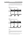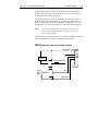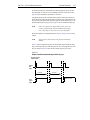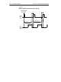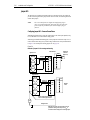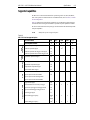
1
User’s Manual KPCI-3101, -3102, -3103, -3104 Series PCI Bus Data Acquisition Boards 98150 Rev. A / 10-99 WARRANTY Hardware Keithley Instruments, Inc. warrants that, for a period of three (3) years from the date of shipment, the Keithley Hardware product will be free from defects in materials or workmanship. This warranty will be honored provided the defect has not been caused by use of the Keithley Hardware not in accordance with the instructions for the product. This warranty shall be null and void upon: (1) any modification of Keithley Hardware that is made by other than Keithley and not approved in writing by Keithley or (2) operation of the Keithley Hardware outside of the environmental specifications therefore. Upon receiving notification of a defect in the Keithley Hardware during the warranty period, Keithley will, at its option, either repair or replace such Keithley Hardware. During the first ninety days of the warranty period, Keithley will, at its option, supply the necessary on site labor to return the product to the condition prior to the notification of a defect. Failure to notify Keithley of a defect during the warranty shall relieve Keithley of its obligations and liabilities under this warranty. Other Hardware The portion of the product that is not manufactured by Keithley (Other Hardware) shall not be covered by this warranty, and Keithley shall have no duty of obligation to enforce any manufacturers' warranties on behalf of the customer. On those other manufacturers’ products that Keithley purchases for resale, Keithley shall have no duty of obligation to enforce any manufacturers’ warranties on behalf of the customer. Software Keithley warrants that for a period of one (1) year from date of shipment, the Keithley produced portion of the software or firmware (Keithley Software) will conform in all material respects with the published specifications provided such Keithley Software is used on the product for which it is intended and otherwise in accordance with the instructions therefore. Keithley does not warrant that operation of the Keithley Software will be uninterrupted or error-free and/ or that the Keithley Software will be adequate for the customer's intended application and/or use. This warranty shall be null and void upon any modification of the Keithley Software that is made by other than Keithley and not approved in writing by Keithley. If Keithley receives notification of a Keithley Software nonconformity that is covered by this warranty during the warranty period, Keithley will review the conditions described in such notice. Such notice must state the published specification(s) to which the Keithley Software fails to conform and the manner in which the Keithley Software fails to conform to such published specification(s) with sufficient specificity to permit Keithley to correct such nonconformity. If Keithley determines that the Keithley Software does not conform with the published specifications, Keithley will, at its option, provide either the programming services necessary to correct such nonconformity or develop a program change to bypass such nonconformity in the Keithley Software. Failure to notify Keithley of a nonconformity during the warranty shall relieve Keithley of its obligations and liabilities under this warranty. Other Software OEM software that is not produced by Keithley (Other Software) shall not be covered by this warranty, and Keithley shall have no duty or obligation to enforce any OEM's warranties on behalf of the customer. Other Items Keithley warrants the following items for 90 days from the date of shipment: probes, cables, rechargeable batteries, diskettes, and documentation. Items not Covered under Warranty This warranty does not apply to fuses, non-rechargeable batteries, damage from battery leakage, or problems arising from normal wear or failure to follow instructions. Limitation of Warranty This warranty does not apply to defects resulting from product modification made by Purchaser without Keithley's express written consent, or by misuse of any product or part. Disclaimer of Warranties EXCEPT FOR THE EXPRESS WARRANTIES ABOVE KEITHLEY DISCLAIMS ALL OTHER WARRANTIES, EXPRESS OR IMPLIED, INCLUDING WITHOUT LIMITATION, ALL IMPLIED WARRANTIES OF MERCHANTABILITY AND FITNESS FOR A PARTICULAR PURPOSE. KEITHLEY DISCLAIMS ALL WARRANTIES WITH RESPECT TO THE OTHER HARDWARE AND OTHER SOFTWARE. Limitation of Liability KEITHLEY INSTRUMENTS SHALL IN NO EVENT, REGARDLESS OF CAUSE, ASSUME RESPONSIBILITY FOR OR BE LIABLE FOR: (1) ECONOMICAL, INCIDENTAL, CONSEQUENTIAL, INDIRECT, SPECIAL, PUNITIVE OR EXEMPLARY DAMAGES, WHETHER CLAIMED UNDER CONTRACT, TORT OR ANY OTHER LEGAL THEORY, (2) LOSS OF OR DAMAGE TO THE CUSTOMER'S DATA OR PROGRAMMING, OR (3) PENALTIES OR PENALTY CLAUSES OF ANY DESCRIPTION OR INDEMNIFICATION OF THE CUSTOMER OR OTHERS FOR COSTS, DAMAGES, OR EXPENSES RELATED TO THE GOODS OR SERVICES PROVIDED UNDER THIS WARRANTY. Keithley Instruments, Inc. • 28775 Aurora Road • Cleveland, OH 44139 • 440-248-0400 • Fax: 440-248-6168 • http://www.keithley.com BELGIUM: CHINA: FRANCE: GERMANY: GREAT BRITAIN: INDIA: ITALY: NETHERLANDS: SWITZERLAND: TAIWAN: Keithley Instruments B.V. Keithley Instruments China Keithley Instruments Sarl Keithley Instruments GmbH Keithley Instruments Ltd Keithley Instruments GmbH Keithley Instruments s.r.l. Keithley Instruments B.V. Keithley Instruments SA Keithley Instruments Taiwan Bergensesteenweg 709 • B-1600 Sint-Pieters-Leeuw • 02/363 00 40 • Fax: 02/363 00 64 Yuan Chen Xin Building, Room 705 • 12 Yumin Road, Dewai, Madian • Beijing 100029 • 8610-62022886 • Fax: 8610-62022892 B.P. 60 • 3, allée des Garays • 91122 Palaiseau Cédex • 01 64 53 20 20 • Fax: 01 60 11 77 26 Landsberger Strasse 65 • D-82110 Germering • 089/84 93 07-40 • Fax: 089/84 93 07-34 The Minster • 58 Portman Road • Reading, Berkshire RG30 1EA • 0118-9 57 56 66 • Fax: 0118-9 59 64 69 Flat 2B, WILOCRISSA • 14, Rest House Crescent • Bangalore 560 001 • 91-80-509-1320/21 • Fax: 91-80-509-1322 Viale S. Gimignano, 38 • 20146 Milano • 02/48 30 30 08 • Fax: 02/48 30 22 74 Postbus 559 • 4200 AN Gorinchem • 0183-635333 • Fax: 0183-630821 Kriesbachstrasse 4 • 8600 Dübendorf • 01-821 94 44 • Fax: 01-820 30 81 6/99 1 Fl. 85 Po Ai Street • Hsinchu, Taiwan, R.O.C. • 886-3572-9077• Fax: 886-3572-9031 KPCI-3101, -3102, -3103, -3104 Series PCI Bus Data Acquisition Board User’s Manual DriverLINX, SSTNET, and LabOBJX are registered trademarks and DriverLINX/VB are trademarks of Scientific Software Tools, Inc. Microsoft and Windows are registered trademarks and Visual C++ and Visual Basic are trademarks of Microsoft Corporation. Borland is a registered trademark and Borland C++, Delphi, and Turbo Pascal are trademarks of Borland International, Inc. IBM is a registered trademark of International Business Machines Corporation. Acrobat is a registered trademark of Adobe Systems Incorporated. All other brand and product names are trademarks or registered trademarks of their respective companies. Copyright © Keithley Instruments, Inc., 1999. All rights reserved. Reproduction or adaptation of any part of this documentation beyond that permitted by Section 117 of the 1979 United States Copyright Act without permission of the Copyright owner is unlawful. ©1999, Keithley Instruments, Inc. All rights reserved. Cleveland, Ohio, U.S.A. First Printing, October 1999 Document Number: 98150 Rev. A Manual Print History The print history shown below lists the printing dates of all Revisions and Addenda created for this manual. The Revision Level letter increases alphabetically as the manual undergoes subsequent updates. Addenda, which are released between Revisions, contain important change information that the user should incorporate immediately into the manual. Addenda are numbered sequentially. When a new Revision is created, all Addenda associated with the previous Revision of the manual are incorporated into the new Revision of the manual. Each new Revision includes a revised copy of this print history page. Revision A (Document Number 98150) ............................................................................................. October 1999 All Keithley product names are trademarks or registered trademarks of Keithley Instruments, Inc. Other brand and product names are trademarks or registered trademarks of their respective holders. Safety Precautions The following safety precautions should be observed before using this product and any associated instrumentation. Although some instruments and accessories would normally be used with non-hazardous voltages, there are situations where hazardous conditions may be present. This product is intended for use by qualified personnel who recognize shock hazards and are familiar with the safety precautions required to avoid possible injury. Read the operating information carefully before using the product. The types of product users are: Responsible body is the individual or group responsible for the use and maintenance of equipment, for ensuring that the equipment is operated within its specifications and operating limits, and for ensuring that operators are adequately trained. Operators use the product for its intended function. They must be trained in electrical safety procedures and proper use of the instrument. They must be protected from electric shock and contact with hazardous live circuits. Maintenance personnel perform routine procedures on the product to keep it operating, for example, setting the line voltage or replacing consumable materials. Maintenance procedures are described in the manual. The procedures explicitly state if the operator may perform them. Otherwise, they should be performed only by service personnel. Service personnel are trained to work on live circuits, and perform safe installations and repairs of products. Only properly trained service personnel may perform installation and service procedures. Exercise extreme caution when a shock hazard is present. Lethal voltage may be present on cable connector jacks or test fixtures. The American National Standards Institute (ANSI) states that a shock hazard exists when voltage levels greater than 30V RMS, 42.4V peak, or 60VDC are present. A good safety practice is to expect that hazardous voltage is present in any unknown circuit before measuring. Users of this product must be protected from electric shock at all times. The responsible body must ensure that users are prevented access and/or insulated from every connection point. In some cases, connections must be exposed to potential human contact. Product users in these circumstances must be trained to protect themselves from the risk of electric shock. If the circuit is capable of operating at or above 1000 volts, no conductive part of the circuit may be exposed. As described in the International Electrotechnical Commission (IEC) Standard IEC 664, digital multimeter measuring circuits (e.g., Keithley Models 175A, 199, 2000, 2001, 2002, and 2010) are Installation Category II. All other instruments’ signal terminals are Installation Category I and must not be connected to mains. Do not connect switching cards directly to unlimited power circuits. They are intended to be used with impedance limited sources. NEVER connect switching cards directly to AC mains. When connecting sources to switching cards, install protective devices to limit fault current and voltage to the card. Before operating an instrument, make sure the line cord is connected to a properly grounded power receptacle. Inspect the connecting cables, test leads, and jumpers for possible wear, cracks, or breaks before each use. For maximum safety, do not touch the product, test cables, or any other instruments while power is applied to the circuit under test. ALWAYS remove power from the entire test system and discharge any capacitors before: connecting or disconnecting cables or jumpers, installing or removing switching cards, or making internal changes, such as installing or removing jumpers. Do not touch any object that could provide a current path to the common side of the circuit under test or power line (earth) ground. Always make measurements with dry hands while standing on a dry, insulated surface capable of withstanding the voltage being measured. The instrument and accessories must be used in accordance with its specifications and operating instructions or the safety of the equipment may be impaired. The WARNING heading in a manual explains dangers that might result in personal injury or death. Always read the associated information very carefully before performing the indicated procedure. Do not exceed the maximum signal levels of the instruments and accessories, as defined in the specifications and operating information, and as shown on the instrument or test fixture panels, or switching card. The CAUTION heading in a manual explains hazards that could damage the instrument. Such damage may invalidate the warranty. When fuses are used in a product, replace with same type and rating for continued protection against fire hazard. Before performing any maintenance, disconnect the line cord and all test cables. Chassis connections must only be used as shield connections for measuring circuits, NOT as safety earth ground connections. If you are using a test fixture, keep the lid closed while power is applied to the device under test. Safe operation requires the use of a lid interlock. If a screw is present, connect it to safety earth ground using the wire recommended in the user documentation. The ! symbol on an instrument indicates that the user should refer to the operating instructions located in the manual. The symbol on an instrument shows that it can source or measure 1000 volts or more, including the combined effect of normal and common mode voltages. Use standard safety precautions to avoid personal contact with these voltages. Instrumentation and accessories shall not be connected to humans. To maintain protection from electric shock and fire, replacement components in mains circuits, including the power transformer, test leads, and input jacks, must be purchased from Keithley Instruments. Standard fuses, with applicable national safety approvals, may be used if the rating and type are the same. Other components that are not safety related may be purchased from other suppliers as long as they are equivalent to the original component. (Note that selected parts should be purchased only through Keithley Instruments to maintain accuracy and functionality of the product.) If you are unsure about the applicability of a replacement component, call a Keithley Instruments office for information. To clean an instrument, use a damp cloth or mild, water based cleaner. Clean the exterior of the instrument only. Do not apply cleaner directly to the instrument or allow liquids to enter or spill on the instrument. Products that consist of a circuit board with no case or chassis (e.g., data acquisition board for installation into a computer) should never require cleaning if handled according to instructions. If the board becomes contaminated and operation is affected, the board should be returned to the factory for proper cleaning/servicing. Rev. 2/99 Table of Contents 1 Overview Features ............................................................................................................................................................... DriverLINX software .......................................................................................................................................... Viewing the KPCI-3101–4 series documentation online.................................................................................... System requirements ........................................................................................................................................... Software .............................................................................................................................................................. Accessories.......................................................................................................................................................... 2 1-2 1-3 1-4 1-5 1-5 1-6 Principles of Operation Analog input features .......................................................................................................................................... 2-2 Input resolution ........................................................................................................................................... 2-3 Analog input channels................................................................................................................................. 2-3 Input ranges and gains................................................................................................................................. 2-4 A/D sample clock sources........................................................................................................................... 2-6 Analog input conversion modes.................................................................................................................. 2-7 Triggers ..................................................................................................................................................... 2-10 Data format ............................................................................................................................................... 2-14 Data transfer .............................................................................................................................................. 2-14 Error conditions......................................................................................................................................... 2-15 Analog output features ...................................................................................................................................... 2-16 Output resolution....................................................................................................................................... 2-16 Analog output channels............................................................................................................................. 2-16 Output ranges and gains ............................................................................................................................ 2-16 Analog output conversion modes.............................................................................................................. 2-17 Data format ............................................................................................................................................... 2-17 Digital I/O features............................................................................................................................................ 2-17 Digital I/O lines......................................................................................................................................... 2-17 Combining or splitting logical channels ................................................................................................... 2-18 Using single value and continuous digital input ....................................................................................... 2-18 Counter/Timer features ..................................................................................................................................... 2-19 Counter/Timer channels ............................................................................................................................ 2-19 C/T Clock sources ..................................................................................................................................... 2-19 Gate types.................................................................................................................................................. 2-21 Pulse outputs ............................................................................................................................................. 2-22 Counter/Timer operation modes ............................................................................................................... 2-22 i 3 Installation and Configuration Unpacking............................................................................................................................................................ 3-2 Installing the software ......................................................................................................................................... 3-2 Software options.......................................................................................................................................... 3-2 Installing DriverLINX ................................................................................................................................. 3-4 Installing application software and drivers.................................................................................................. 3-4 Installing the board .............................................................................................................................................. 3-5 Setting up the computer............................................................................................................................... 3-5 Selecting an expansion slot ......................................................................................................................... 3-5 Inserting the KPCI-3101–4 series board in the computer ........................................................................... 3-6 Configuring the board to work with DriverLINX ............................................................................................... 3-7 Checking the combined board and DriverLINX installations ..................................................................... 3-7 Attaching the STA-300 screw terminal panel ..................................................................................................... 3-8 Jumper W1................................................................................................................................................. 3-10 Resistors .................................................................................................................................................... 3-11 Screw terminal assignments ...................................................................................................................... 3-11 Power......................................................................................................................................................... 3-14 Wiring signals.................................................................................................................................................... 3-14 Connecting analog input signals................................................................................................................ 3-15 Connecting analog output signals.............................................................................................................. 3-19 Connecting digital I/O signals ................................................................................................................... 3-20 Connecting counter/timer signals .............................................................................................................. 3-21 Attaching the STP-68 screw terminal panel ...................................................................................................... 3-25 4 Testing the Board DriverLINX analog I/O panel ............................................................................................................................. 4-2 5 Calibration Introduction ......................................................................................................................................................... 5-2 Objectives .................................................................................................................................................... 5-2 Calibration summary ................................................................................................................................... 5-2 Equipment.................................................................................................................................................... 5-2 Calibration procedure .................................................................................................................................. 5-3 Preparing for the calibrations ...................................................................................................................... 5-3 Calibrating the analog inputs....................................................................................................................... 5-3 Calibrating the analog outputs..................................................................................................................... 5-3 6 Troubleshooting General checklist ................................................................................................................................................. 6-2 Using the DriverLINX event viewer ................................................................................................................... 6-2 Device initialization error messages............................................................................................................ 6-2 Problem isolation................................................................................................................................................. 6-3 Troubleshooting table.......................................................................................................................................... 6-4 Testing the board and host computer................................................................................................................... 6-5 Testing the accessory slot and I/O connections................................................................................................... 6-5 Technical support ................................................................................................................................................ 6-6 Returning equipment to Keithley ........................................................................................................................ 6-7 ii A Specifications Supported capabilities ........................................................................................................................................ A-9 B Connector Pin Assignments C Systematic Problem Isolation Problem isolation Scheme A: basic system ............................................................................................... C-3 Problem isolation Scheme B: installation .................................................................................................. C-5 Problem isolation Scheme C: application software ................................................................................. C-10 Problem isolation Scheme D: expansion slot connectors ........................................................................ C-12 Problem isolation Scheme E: user wiring ................................................................................................ C-13 Problem isolation Scheme F: the board ................................................................................................... C-13 Problem isolation Scheme G: verification of problem solution............................................................... C-13 Specified hardware I/O tests ............................................................................................................................ C-14 Analog input hardware test ...................................................................................................................... C-14 Analog output hardware test .................................................................................................................... C-17 General-purpose digital I/O hardware test ............................................................................................... C-20 Specified software I/O tests ............................................................................................................................. C-20 Analog input software test ....................................................................................................................... C-20 Analog output software test ..................................................................................................................... C-22 General-purpose digital I/O software test ................................................................................................ C-25 iii iv List of Illustrations 2 Principles of Operation Figure 2-1 Figure 2-2 Figure 2-3 Figure 2-4 Figure 2-5 Figure 2-6 Figure 2-7 Figure 2-8 Figure 2-9 Figure 2-10 Figure 2-11 Figure 2-12 Figure 2-13 Figure 2-14 Figure 2-15 Figure 2-16 Figure 2-17 Figure 2-18 Figure 2-19 Figure 2-20 Figure 2-21 Figure 2-22 Block diagram of the KPCI-3101–4 series boards...................................................................................... 2-2 Continuous post-trigger mode without triggered scan .............................................................................. 2-11 Continuous post-trigger mode with triggered scan ................................................................................... 2-11 Continuous pre-trigger mode .................................................................................................................... 2-12 Continuous pre-trigger mode with triggered scan..................................................................................... 2-12 Continuous about-trigger mode ................................................................................................................ 2-13 Continuous about-trigger mode with triggered scan................................................................................ 2-14 Counter/Timer channel ............................................................................................................................ 2-19 Example of a Low-to-High pulse output type........................................................................................... 2-22 Connecting event counting signals (shown for clock input 0 and external gate 0)................................... 2-23 Example of event counting ....................................................................................................................... 2-24 Connecting frequency measurement signals without an external gate input (shown for clock input 0) .. 2-24 Connecting frequency measurement signals (shown for clock input 0 and external gate 0).................... 2-25 Example of frequency measurement......................................................................................................... 2-26 Connecting rate generation sIgnals (shown for counter 0; a software gate is used) ................................. 2-27 Example of rate generation mode with a 75% duty cycle........................................................................ 2-28 Example of rate generation mode with a 25% duty cycle......................................................................... 2-28 Connecting one-shot signals (shown for counter output 0 and gate 0) ..................................................... 2-29 Example of one-shot mode using a 99.99% duty cycle ............................................................................ 2-30 Example of one-shot mode using a 50% duty cycle ................................................................................. 2-30 Example of repetitive one-shot mode using a 99.99% duty cycle ............................................................ 2-31 Example of repetitive one-shot mode using a 50% duty cycle ................................................................. 2-32 v 3 Installation and Configuration Figure 3-1 Figure 3-2 Figure 3-3 Figure 3-4 Figure 3-5 Figure 3-6 Figure 3-7 Figure 3-8 Figure 3-9 Figure 3-10 Figure 3-11 Figure 3-12 Figure 3-13 Figure 3-14 Figure 3-15 Figure 3-16 Figure 3-17 Figure 3-18 Figure 3-19 Figure 3-20 Inserting the KPCI-3101–4 series board in the computer ........................................................................... 3-6 Attaching the STA-300 screw terminal panel to a KPCI-3101–4 series board........................................... 3-8 Layout of the STA-300 screw terminal panel ............................................................................................. 3-9 Removal of jumper W1 for remote ground sensing .................................................................................. 3-10 Connecting single-ended voltage inputs (shown for channels 0, 1, and 8) ............................................... 3-15 Connecting pseudo-differential voltage inputs (shown for channels 0, 1, and 8) ..................................... 3-16 Connecting differential voltage inputs (shown for channel 0) .................................................................. 3-17 Connecting differential voltage inputs from a grounded signal source (shown for channel 0) ................ 3-18 Connecting current inputs (shown for channel 0) ..................................................................................... 3-18 Connecting analog output voltages using an external +10V reference (shown for channel 0) ................. 3-19 Connecting analog output voltages using the board’s internal +10V reference (shown for channel 0) ... 3-19 Connecting digital inputs (shown for channels 0 and 1, port A)............................................................... 3-20 Connecting digital outputs (shown for channel 0, port B) ........................................................................ 3-20 Connecting event counting signals (shown for clock input 0 and external gate 0) ................................... 3-21 Connecting event counting signals without an external gate input (shown for clock input 0) ................. 3-22 Cascading counters (shown for event counting using counters 0 and 1 and external gate 0) ................... 3-22 Connecting frequency measurement signals (shown for clock input 0 and external gate 0) .................... 3-23 Connecting pulse output signals (shown for counter output 0 and gate 0) ............................................... 3-23 Cascading counters (shown for rate generation using counters 0 and 1 and external gate 0) ................... 3-24 Cascading counters (shown for one-shot using counters 0 and 1 and external gate 1) ............................. 3-24 vi List of Tables 1 Overview Table 1-1 Table 1-2 Differences among KPCI-3101–4 Series boards ........................................................................................ 1-2 System requirements ................................................................................................................................... 1-5 2 Principles of Operation Table 2-1 Table 2-2 Table 2-3 Table 2-4 Table 2-5 Table 2-6 Supported analog input resolutions............................................................................................................. 2-3 Gains and effective ranges .......................................................................................................................... 2-5 Maximum frequency supported .................................................................................................................. 2-6 Maximum retrigger frequency .................................................................................................................... 2-8 Supported analog output resolutions . . .................................................................................................... 2-16 Extended channel addressing of digital I/O channels using DriverLINX................................................. 2-18 3 Installation and Configuration Table 3-1 Table 3-2 Table 3-3 Analog input screw terminal assignments on the STA-300...................................................................... 3-12 Analog output and power screw terminal assignments on the STA-300 .................................................. 3-13 Counter/Timer and digital I/O screw terminal assignments on the STA-300........................................... 3-13 6 Troubleshooting Table 6-1 Troubleshooting problems .......................................................................................................................... 6-4 A Specifications Table A-1 Table A-2 Table A-3 Table A-4 Table A-5 Table A-6 Table A-7 Table A-8 Table A-9 A/D subsystem specifications .................................................................................................................... D/A subsystem specifications .................................................................................................................... DIN/DOUT subsystem specifications........................................................................................................ C/T subsystem specifications..................................................................................................................... Power, physical, and environmental specifications ................................................................................... Connector specifications ............................................................................................................................ STA-300 specifications.............................................................................................................................. CAB-305 cable specifications.................................................................................................................... KPCI-3101–4 series supported options...................................................................................................... A-2 A-4 A-5 A-6 A-7 A-7 A-8 A-8 A-9 vii B Connector Pin Assignments Table B-1 Table B-2 Table B-3 Pin assignments for connector J1 on the KPCI-3101–4 series boards ....................................................... B-2 Pin assignments for connector J1 on the STA-300 .................................................................................... B-3 Pin assignments for connector J2 on the STA-300 .................................................................................... B-4 C Systematic Problem Isolation Table C-1 Wiring for analog input hardware test using an STA-300 screw terminal accessory connected to the Analog I/O connections ........................................................................................................... C-15 Terminals on STA-300 screw terminal accessory to which DVM/DMM will be connected during analog output hardware test.................................................................................................... C-17 Test connections and correct readings for zero-voltage analog output, using an STA-300 screw terminal accessory connected to J1.................................................................................................... C-19 Test connections and correct readings for mid-range analog output, using an STA-300 screw terminal accessory connected to the upper “Analog” I/O connector ................................................. C-19 Wiring for analog input hardware test using an STA-300 screw terminal accessory connected to the Analog I/O connections ........................................................................................................... C-21 Terminals on STA-300 screw terminal accessory to which DVM/DMM will be connected during analog output hardware test.................................................................................................... C-23 Test connections and correct readings for zero-voltage analog output, using an STA-300 screw terminal accessory connected to J1.................................................................................................... C-24 Test connections and correct readings for mid-range analog output, using an STA-300 screw terminal accessory connected to the KPCI-3101–4 board ................................................................. C-24 Table C-2 Table C-3 Table C-4 Table C-5 Table C-6 Table C-7 Table C-8 viii 1 Overview 1-2 Overview KPCI-3101 — KPCI-3104 Series User’s Manual Features The KPCI-3101–4 Series is a family of low-cost, multifunction data acquisition boards for the PCI bus. The KPCI-3101–4 Series consists of the following boards: KPCI-3101, KPCI-3102, KPCI-3103, and KPCI-3104. These board types differ in analog I/O resolution, analog input sample frequency, analog input ranges, and the number of analog output channels, as shown in Table 1-1. Table 1-1 Differences among KPCI-3101–4 Series boards Board Type Analog I/O Resolution Analog Input Sample Frequency Analog Input Ranges1 Analog Output Channels KPCI-3101 12 bit 225kHz ±10V, 0 to 10V 0 KPCI-3102 12 bit 225kHz ±10V, 0 to 10V 2 KPCI-3103 12 bit 400kHz ±10V, 0 to 10V 0 KPCI-3104 12 bit 400kHz ±10V, 0 to 10V 2 1 Assumes a gain of 1. Using these ranges with gains of 2, 4, or 8 yields a number of effective input ranges; refer to page 2-4 for more information. All KPCI-3101–4 Series boards share the following major features: • PCI bus mastering capability for analog inputs • 16 single-ended or pseudo-differential analog input channels, or 8 differential analog input channels (for information on pseudo-differential analog input channels, see “Connecting pseudo-differential voltage inputs” in Section 3) • Signal conditioning through connections to 5B Series backplanes • Input gains of 1, 2, 4, and 8 • Continuously-paced and triggered scan capability • A 1024-location channel-gain list that supports sampling analog input channels at the same or different gains in sequential or random order • Up to 256 scans per trigger for a total of 262,144 samples per trigger in triggered scan mode • Internal and external clock sources for the analog input subsystem • Digital TTL triggering for the analog input subsystem • Software calibration of the analog I/O circuitry • Two 8-bit digital ports programmable as inputs or outputs on a per-port basis; digital input lines from these lines can be included as part of the analog input channel-gain list to correlate the timing of analog and digital events; digital outputs can drive external solid-state relays • One 7-bit digital I/O port programmable as a general-purpose (non-clocked) input or output port • Four user counter/timers programmable for event counting, frequency measurement, rate generation (continuous pulse output), one-shot pulse output, and repetitive one-shot pulse output • Programmable gate types • Programmable pulse output polarities (output types) and duty cycles For a discussion of these features in detail, refer to Section 2. KPCI-3101 — KPCI-3104 Series User’s Manual Overview 1-3 DriverLINX software The following software is available for use with the KPCI-3101–4 Series board: • KPCI-3101–4 Series standard software package — Shipped with KPCI-3101–4 Series boards. Includes DriverLINX for Microsoft Windows and function libraries for writing application programs under Windows in a high-level language such as C/C++, Visual Basic, Delphi, and Test Point; LabVIEW support files; utility programs; and language-specific example programs. • DriverLINX — the high-performance real-time data-acquisition device drivers for Windows application development includes: • DriverLINX API DLLs and drivers supporting the KPCI-3101–4 Series hardware • Analog I/O Test Panel — a DriverLINX program that verifies the installation and operation of your KPCI-3101–4 Series board and demonstrates several virtual bench-top instruments • Learn DriverLINX — an interactive learning and demonstration program for DriverLINX that includes a Digital Storage Oscilloscope • Source Code — for the sample programs • DriverLINX Application Programming Interface files — for the KPCI-3101–4 Series interfaces • DriverLINX Calibration Utility — used to calibrate the ADC and DAC functions of the KPCI-3101–4 Series board • DriverLINX On-line Help System — provides immediate help as you operate DriverLINX • Supplemental Documentation — on DriverLINX installation and configuration; analog and digital I/O programming; counter/timer programming; technical reference; and information specific to the KPCI-3101–4 Series hardware. 1-4 Overview KPCI-3101 — KPCI-3104 Series User’s Manual Viewing the KPCI-3101–4 series documentation online The DriverLINX Manuals and this manual have been provided in electronic form (in PDF file format) on the KPCI-3101–4 Series CD-ROM. To view these documents, you need to install Rev 3.01 or later of Adobe Acrobat Reader on your hard drive (refer to DriverLINX for installation instructions). View the KPCI-3101–4 Series documentation by clicking the manual title. Here are a few helpful hints about using Adobe Acrobat Reader: • To navigate to a specific section of the document, click a heading from the table of contents on the left side of the document. • Within the document, click the text shown in blue to jump to the appropriate reference (the pointer changes from a hand to an index finger). • To go back to the page from which the jump was made, click the right mouse button and Go Back, or from the main menu, click View, then Go Back. • To print the document, from the main menu, click File, then Print. • To increase or decrease the size of the displayed document, from the main menu, click View, then Zoom. • By default, text and monochrome images are smoothed in Acrobat Reader, resulting in blurry images. If you wish, you can turn smoothing off by clicking File, then Preferences/ General, and unchecking Smooth Text and Monochrome Images. KPCI-3101 — KPCI-3104 Series User’s Manual Overview 1-5 System requirements The system capabilities required to run the KPCI-3101–4 Series board, and to use the DriverLINX software supplied with the board, are listed in Table 1-2. Table 1-2 System requirements CPU Type Pentium or higher processor on motherboard with PCI bus version 2.1 Operating system Windows 95 or 98 Windows NT version 4.0 or higher Memory 16 MB or greater RAM when running Windows 95 or 98 32 MB or greater RAM when running Windows NT Hard disk space 4 MB for minimum installation 50 MB for maximum installation Other A CD-ROM drive* A free PCI-bus expansion slot capable of bus mastering Enough reserve computer power supply capacity to power the KPCI-3101–4 Series board, which draws 0.9A at 5VDC and 48mA at +12VDC. A VGA, or compatible, display (640 x 480 or higher, 256 colors recommended) *Any CD-ROM drive that came installed with the required computer should be satisfactory. However, if you have post-installed an older CD-ROM drive or arrived at your present system by updating the microprocessor or replacing the motherboard, some early CD-ROM drives may not support the long file names often used in 32 bit Windows files. Software The user can select a fully integrated data acquisition software package such as TestPoint or LabVIEW or write a custom program supported by DriverLINX. DriverLINX is the basic Application Programming Interface (API) for the KPCI-3101–4 Series boards: • It supports programmers who wish to create custom applications using Visual C/C++, Visual Basic, or Delphi. • It accomplishes foreground and background tasks to perform data acquisition. • It is the needed interface between TestPoint and LabVIEW and a KPCI-3101–4 Series board. DriverLINX software and user’s documentation on a CD-ROM are included with your board. TestPoint is an optional, fully featured, integrated application package with a graphical dragand-drop interface which can be used to create data acquisition applications without programming. LabVIEW is an optional, fully featured graphical programming language used to create virtual instrumentation. Refer to Section 3, “Installation and Configuration” for more information about DriverLINX, TestPoint, and LabView. 1-6 Overview KPCI-3101 — KPCI-3104 Series User’s Manual Accessories The following optional accessories are available for the KPCI-3101–4 Series board: • STA-300 screw terminal panel — Screw terminal panel with two connectors. The STP-300 includes features such as jumpers for selecting AMP LO connections for use with “pseudodifferential” input; convenient locations for addition of bias return resisters for use when measuring floating inputs in differential mode; convenient locations for current sense shunt resistors for sensing current loops. Connector J1 accommodates the analog and digital I/O signals from the KPCI-3101–4 Series board, and connector J2 allows you to connect 5B signal conditioning backplanes. In addition, the STA-300, in conjunction with the CAB-305 cable, is the configuration in which KPCI-3101–4 was tested for CE emissions. • STP-68 screw terminal panel — Screw terminal panel with one connector. The 68-pin connector accommodates the analog and digital I/O signals from the KPCI-3101–4 Series board. The screw terminals are wired so that when connected using a CAB-305 cable, the terminal number corresponds to a terminal number on the attached plug-in board. The STP-68 is not shielded and was not used in CE emission testing. • CAB-305 cable — A 2-meter, twisted pair, shielded cable that connects the 68-pin connector (J1) on the KPCI-3101–4 Series board to the J1 connector on the STA-300 screw terminal panel or to the 68-pin connector on the STP-68 screw terminal panel. 2 Principles of Operation 2-2 Principles of Operation KPCI-3101 — KPCI-3104 Series User’s Manual This section describes the analog input, analog output, digital I/O, and counter/timer features of the KPCI-3101–4 Series board. To frame the discussions, refer to the block diagram shown in Figure 2-1. Note that bold entries indicate signals you can access. Figure 2-1 Block diagram of the KPCI-3101–4 series boards Ext A/D Clock Ext TTL Trig Trigger/Clock Logic A/D Clk A/D Counter, 24-bits TScan Counter 24-bit 20 MHz Clock Analog In Ch. Sel Gain Sel A/D Clk DIO Ports A and B Input Sel Ch. Sel Gain Sel Input Sel CGL Reg. Channel Parameter Reg. 1 K Entry CGL FIFO 16 Channel Mux Discard sample Bidirectional 8-bit Latch Bidirectional 8-bit Latch Gain Amp (1, 2, 4, 8) 20 MHz Clock ADC SW_Clk1 Tristate Buffers SW_Clk0 Ser_Da 1 kSample Input FIFO Ser_Clk PCI Bus Interface PCI Bus DIO Port B [7:0] DIO Port A [7:0] User Clk [3:0] 4 User Counter/ Timers, 16-bit ea. User Gate [3:0] User Out [3:0] Multiplying DAC* Analog Output 1 Multiplying DAC* Analog Output 0 DIO Port C [6:0] *DACs not included on KPCI-3101, or KPCI-3103 boards. Analog input features This section describes the features of the analog input (A/D) subsystem, including the following: • • • • • • • • Input resolution Analog input channels Input ranges and gains A/D sample clock sources Analog input conversion modes Trigger sources and trigger acquisition modes Data formats and transfer Error conditions KPCI-3101 — KPCI-3104 Series User’s Manual Principles of Operation 2-3 Input resolution Table 2-1 lists the input resolutions supported by the KPCI-3101–4 Series boards. The resolution is fixed for each board type; therefore, it cannot be programmed in software. Table 2-1 Supported analog input resolutions Board Type Supported Resolution KPCI-3101 12 bits KPCI-3102 12 bits KPCI-3103 12 bits KPCI-3104 12 bits Analog input channels The KPCI-3101–4 Series board supports 16 single-ended or pseudo-differential analog input channels, or 8 differential analog input channels on board. Refer to Section 3, “Wiring signals” for a description of how to wire these signals. You configure the channel type through DriverLINX software. NOTE For pseudo-differential inputs, specify single-ended in software; in this case, how you wire these signals determines the configuration. Choose this configuration when noise or common-mode voltage (the difference between the ground potentials of the signal source and the ground of the STA-300 screw terminal panel or between the grounds of other signals) exists and the differential configuration is not suitable for your application. This option provides less noise rejection than the differential configuration; however, all 16 analog input channels are available. The KPCI-3101–4 Series board can acquire data from a single analog input channel or from a group of analog input channels. Onboard channels are numbered 0 to 15 for single-ended and pseudo-differential inputs or 0 to 7 for differential inputs. The following subsections describe how to specify the channels. Specifying a single channel The simplest way to acquire data from a single channel is to specify the channel for a single value analog input operation using software; refer to page 2-7 for more information on single value operations. You can also specify a single channel using the analog input channel list, described in the next section. 2-4 Principles of Operation KPCI-3101 — KPCI-3104 Series User’s Manual Specifying one or more channels On the KPCI-3101–4 Series board, you can read data from one or more analog input channels using an analog input channel list. You can group the channels in the list sequentially (either starting with 0 or with any other analog input channel) or randomly. You can also specify a single channel or the same channel more than once in the list. Using DriverLINX software, specify the channels in the order you want to sample them. The analog input channel list corresponds to the Channel-Gain List FIFO (first-in, first-out buffer) on the board. You can enter up to 1,024 entries in the channel list. The channels are read in order (using continuous paced mode or triggered scan mode) from the first entry to the last entry in the channel list. You can read the channels in the channel list up to 256 times per trigger (for a total of 262,144 samples per trigger) using triggered scan mode. Refer to page 2-7 for more information on the supported conversion modes. Specifying digital input lines in the analog input channel list In addition to the analog input channels, the KPCI-3101–4 Series board allows you to read 16 digital I/O lines (Port A, lines 0 to 7 and Port B, lines 0 to 7) using the analog input channel list. This feature is particularly useful when you want to correlate the timing of analog and digital events. To read these 16 digital I/O lines, specify channel 0 in the DriverLINX analog input channel list with a special gain modifier. Refer to the DriverLINX Analog I/O Programming Guide, provided with DriverLINX. NOTE If channel 0 is programmed with digital capabilities and is the only channel in the channel-gain list, the board can read this channel at a rate of 3MSamples/s. Refer to the DriverLINX Analog I/O Programming Guide, provided with DriverLINX. The digital channel is treated like any other channel in the analog input channel list; therefore, all the clocking, triggering, and conversion modes supported for analog input channels are supported for these digital I/O lines, if you specify them in this manner. Input ranges and gains Each channel on the KPCI-3101, KPCI-3102, KPCI-3103, and KPCI-3104 board can measure unipolar and bipolar analog input signals. A unipolar signal is always positive (0 to 10V on a KPCI-3101–4 Series board), while a bipolar signal extends between the negative and positive peak values (±10V on a KPCI-3101–4 Series board). Through software, specify the range as 0 to 10V for unipolar signals or −10V to +10V for bipolar signals. Note that you specify the range for the entire analog input subsystem, not the range per channel. KPCI-3101 — KPCI-3104 Series User’s Manual Principles of Operation 2-5 KPCI-3101–4 Series boards provide gains of 1, 2, 4, and 8, which are programmable per channel. Table 2-2 lists the effective ranges supported by the KPCI-3101–4 Series board using these gains. Table 2-2 Gains and effective ranges Gain Unipolar Analog Input Range Bipolar Analog Input Range 1 0 to 10V ±10V 2 0 to 5V ±5V 4 0 to 2.5V ±2.5V 8 0 to 1.25V ±1.25V For each channel, choose the gain that has the smallest effective range that includes the signal you want to measure. For example, if the range of your analog input signal is ±1.5V, specify a range of −10V to +10V for the board and use a gain of 4 for the channel; the effective input range for this channel is then ±2.5V, which provides the best sampling accuracy for that channel. The way you specify gain depends on how you specified the channels, as described in the following subsections. Specifying the gain for a single channel The simplest way to specify the gain for a single channel is to specify the gain for a single value analog input operation using software; refer to page 2-7 for more information on single value operations. You can also specify the gain for a single channel using an analog input gain list, described in the next section. Specifying the gain for one or more channels For KPCI-3101–4 Series boards, you can specify the gain for one or more analog input channels using an analog input gain list. Using software, set up the gain list by specifying the gain for each entry in the channel list. The gain list parallels the channel list. (The two lists together are often referred to as the channel-gain list.) For example, assume the analog input channel list contains three entries: channels 5, 6, and 7; the gain list might look like this: 2, 4, 1, where a gain of 2 corresponds to channel 5, a gain of 4 corresponds to channel 6, and a gain of 1 corresponds to channel 7. NOTE For analog input channel 0 programmed with digital capabilities (the 16 digital I/O lines). Refer to the DriverLINX Analog I/O Programming Guide, provided with DriverLINX. 2-6 Principles of Operation KPCI-3101 — KPCI-3104 Series User’s Manual A/D sample clock sources The KPCI-3101–4 Series board provides two clock sources for pacing analog input operations in continuous mode: • An internal A/D sample clock that uses the 24-bit A/D Counter on the board; and • An external A/D sample clock that you can connect to the screw terminal panel. You use an A/D sample clock to pace the acquisition of each channel in the channel-gain list; this clock is also called the A/D pacer clock. NOTE If you specify Digital Capabilities for channel 0, the A/D sample clock (internal or external) also paces the acquisition of the 16 digital input lines. Refer to the DriverLINX Analog I/O Programming Guide, provided with DriverLINX. The following subsections describe the internal and external A/D sample clocks in more detail. Internal A/D sample clock The internal A/D sample clock uses a 20MHz time base. Conversions start on the falling edge of the counter output; the output pulse is active low. Using software, specify the clock source as internal and the clock frequency at which to pace the operation. The minimum frequency supported is 1.2Hz (1.2 Samples/s); the maximum frequency supported differs depending on the board type, as shown in Table 2-3. Table 2-3 Maximum frequency supported Board Type Maximum Frequency KPCI-3101 225kHz KPCI-3102 225kHz KPCI-3103 400kHz KPCI-3104 400kHz According to sampling theory (Nyquist Theorem), specify a frequency that is at least twice as fast as the input’s highest frequency component. For example, to accurately sample a 20kHz signal, specify a sampling frequency of at least 40kHz. Doing so avoids an error condition called aliasing, in which high frequency input components erroneously appear as lower frequencies after sampling. NOTE If input channel 0 is programmed for Digital Capabilities, and is the only channel programmed, the maximum frequency is 3MHz (3MSamples/s). Refer to the DriverLINX Analog I/O Programming Guide, provided with DriverLINX. KPCI-3101 — KPCI-3104 Series User’s Manual Principles of Operation 2-7 External A/D sample clock The external A/D sample clock is useful when you want to pace acquisitions at rates not available with the internal A/D sample clock or when you want to pace at uneven intervals. Connect an external A/D sample clock to screw terminal TB48 on the STA-300 screw terminal panel (pin 22 on connector J1). Conversions start on the falling edge of the external A/D sample clock input signal. Using software, specify the clock source as external. (Refer to the DriverLINX Analog I/O Programming Guide provided with DriverLINX.) For the KPCI-3101–4 Series board, the clock frequency is always equal to the frequency of the external A/D sample clock input signal that you connect to the board through the screw terminal panel. Analog input conversion modes KPCI-3101–4 Series boards support the following conversion modes: • Single value operations are the simplest to use but offer the least flexibility and efficiency. Using software, you can specify the range, gain, and analog input channel (among other parameters); acquire the data from that channel; and convert the result. The data is returned immediately. For a single value operation, you cannot specify a clock source, trigger source, trigger acquisition mode, scan mode, or buffer. Single value operations stop automatically when finished; you cannot stop a single value operation. • Scan mode takes full advantage of the capabilities of the KPCI-3101–4 Series boards. In a scan, you can specify a channel-gain list, clock source, trigger source, trigger acquisition mode, scan mode, buffer, and buffer wrap mode using software. Two scan modes are supported: continuously-paced scan mode and triggered scan mode. These modes are described in the following subsections. Using DriverLINX software, you can stop a scan when the hardware fills the host buffer you specified or when your application issues a stop command. Continuously-Paced scan mode Use continuously-paced scan mode if you want to accurately control the period between conversions of individual channels in a scan. When it detects an initial trigger, the board cycles through the channel-gain list, acquiring and converting the value for each entry in the channel list (this process is defined as the scan). The board then wraps to the start of the channel-gain list and repeats the process continuously until either the allocated buffers are filled or until you stop the operation. Refer to page 2-14 for more information on buffers. The conversion rate is determined by the frequency of the A/D sample clock; refer to page 2-6 for more information on the A/D sample clock. The sample rate, which is the rate at which a single entry in the channel-gain list is sampled, is determined by the frequency of the A/D sample clock divided by the number of entries in the channel-gain list. To select continuously-paced scan mode, use software to specify the dataflow as continuous, continuous pre-trigger, or continuous about-trigger. The initial trigger source depends on the trigger acquisition mode you use. Refer to page 2-10 for more information on the supported trigger sources and trigger acquisition modes. 2-8 Principles of Operation KPCI-3101 — KPCI-3104 Series User’s Manual Triggered scan mode KPCI-3101–4 Series boards support two triggered scan modes: internally-retriggered and externally-retriggered. These modes are described in the following subsections. Internally-Retriggered Scan Mode Use internally-retriggered scan mode if you want to accurately control both the period between conversions of individual channels in a scan and the period between each scan. This mode is useful when synchronizing or controlling external equipment, or when acquiring a buffer of data on each trigger or retrigger. Using this mode, you can acquire up to 262,144 samples per trigger (256 times per trigger x 1024-location channel-gain list). When it detects an initial trigger, the KPCI-3101–4 Series board scans the channel-gain list a specified number of times (up to 256), then waits for an internal retrigger to occur. When it detects an internal retrigger, the board scans the channel-gain list the specified number of times, then waits for another internal retrigger to occur. The process repeats continuously until either the allocated buffers are filled or until you stop the operation; refer to page 2-14 for more information on buffers. The sample rate is determined by the frequency of the A/D sample clock divided by the number of entries in the channel-gain list; refer to page 2-6 for more information on the A/D sample clock. The conversion rate of each scan is determined by the frequency of the internal retrigger clock. The internal retrigger clock is the Triggered Scan Counter on the board; the Triggered Scan Counter is a 24-bit counter with a 20 MHz clock. Using DriverLINX software, specify the frequency of the internal retrigger clock. The minimum retrigger frequency is 1.2Hz (1.2 Samples/s). Table 2-4 lists the maximum retrigger frequency supported by the KPCI-3101–4 Series boards. Table 2-4 Maximum retrigger frequency Board Maximum Retrigger Frequency KPCI-3101/3102 155kHz KPCI-3103/3104 219kHz The appropriate retrigger frequency depends on a number of factors, determined by the following equations: No. of CGL entries × No. of CGLs per trigger Min. Retrigger Period = ---------------------------------------------------------------------------------------------------------------- + 2µs A/D sample clock frequency 1 Max. Retrigger = ------------------------------------------------------------------------------Frequency Min. Retrigger Period For example, if you are using 16 channels in the channel-gain list (CGL), scanning the channelgain list 256 times every trigger or retrigger, and using an A/D sample clock with a frequency of 100kHz, set the maximum retrigger frequency to 24.41Hz, since 1 24.41Hz = ----------------------------------------------( 16 × 256 --------------------------) + 2µs 100kHz KPCI-3101 — KPCI-3104 Series User’s Manual Principles of Operation 2-9 To select internally-retriggered scan mode, use software to specify the following parameters: • • • • • The dataflow as continuous, continuous pre-trigger, or continuous about-trigger Triggered scan mode usage as enabled The retrigger mode as internal The number of times to scan per trigger or retrigger (also called the multiscan count) The frequency of the retrigger clock The initial trigger source depends on the trigger acquisition mode you use; refer to page 2-10 for more information on the supported and trigger sources and trigger acquisition modes. Externally-Retriggered scan mode Use externally-retriggered scan mode if you want to accurately control the period between conversions of individual channels and retrigger the scan based on an external event. Like internal retrigger scan mode, this mode allows you to acquire 262,144 samples per trigger (256 times per trigger€×1024-location channel-gain list). NOTE Use externally-retriggered scan mode with continuous post-trigger acquisitions only; refer to page 2-10 for more information on posttrigger acquisitions. When a KPCI-3101–4 Series board detects an initial trigger (post-trigger source only), the board scans the channel-gain list up to 256 times, then waits for an external retrigger to occur. You can specify any supported post-trigger source as the initial trigger. Specify the external digital (TTL) trigger for the retrigger. When the retrigger occurs, the board scans the channel-gain list the specified number of times, then waits for another external retrigger to occur. The process repeats continuously until either the allocated buffers are filled (if buffer wrap mode is none) or until you stop the operation (if buffer wrap mode is single or multiple); refer to page 2-14 for more information on buffers. The conversion rate of each channel is determined by the frequency of the A/D sample clock; refer to page 2-6 for more information on the A/D sample clock. The conversion rate of each scan is determined by the period between external retriggers; therefore, it cannot be accurately controlled. The board ignores external triggers that occur while it is acquiring data. Only external retrigger events that occur when the board is waiting for a retrigger are detected and acted on. To select externally-retriggered scan mode, use software to specify the following parameters: • • • • • The dataflow as continuous (post-trigger) The triggered scan mode usage as enabled The retrigger mode as an external retrigger The number of times to scan per trigger or retrigger (also called the multiscan count) The retrigger source as the external digital (TTL) trigger 2-10 Principles of Operation KPCI-3101 — KPCI-3104 Series User’s Manual Triggers A trigger is an event that occurs based on a specified set of conditions. The KPCI-3101–4 Series boards support a number of trigger sources and trigger acquisition modes, described in the following subsections. Trigger sources The KPCI-3101–4 Series board supports a software trigger and an external digital (TTL) trigger. A software trigger event occurs when you start the analog input operation (the computer issues a write to the board to begin conversions). Specify the software trigger source in software. An external digital trigger event occurs when the KPCI-3101–4 Series board detects either a rising or falling edge on the External TTL Trigger input signal connected to screw terminal TB46 on the STA-300 screw terminal panel (pin 56 of connector J1). The trigger signal is TTL-compatible. Using software, specify the trigger source as a rising-edge external digital trigger or falling-edge external digital trigger. Trigger acquisition modes KPCI-3101–4 Series boards can acquire data in post-trigger mode, pre-trigger mode, or abouttrigger mode. These trigger acquisition modes are described in more detail in the following subsections. Post-Trigger acquisition Use post-trigger acquisition mode (continuous mode) when you want to acquire data when a post-trigger or retrigger, if using triggered scan mode, occurs. Using DriverLINX software, specify • The dataflow as continuous, and • The trigger source to start the post-trigger acquisition (the post-trigger source) as any of the supported trigger sources. Refer to page 2-7 for more information on the supported conversion modes; refer to page 2-10 for information on the supported trigger sources. Post-trigger acquisition starts when the board detects the post-trigger event and stops when the specified number of post-trigger samples has been acquired or when you stop the operation. If you are using triggered scan mode, the board continues to acquire post-trigger data using the specified retrigger source to clock the operation. Refer to page 2-8 for more information on triggered scan mode. Figure 2-2 illustrates continuous post-trigger mode using a channel-gain list with three entries: channel 0, channel 1, and channel 2. Triggered scan mode is disabled. In this example, posttrigger analog input data is acquired on each clock pulse of the A/D sample clock. When it reaches the end of the channel-gain list, the board wraps to the beginning of the channel-gain list and repeats this process. Data is acquired continuously (continuously-paced scan mode). KPCI-3101 — KPCI-3104 Series User’s Manual Principles of Operation 2-11 Figure 2-2 Continuous post-trigger mode without triggered scan Chan 2 Chan 0 Chan 1 Chan 2 Chan 0 Chan 1 Chan 2 Chan 0 Chan 1 Chan 2 Chan 0 Chan 1 A/D Sample Clock Post-trigger event occurs. Post-trigger data acquired continuously. Figure 2-3 illustrates the same example using triggered scan mode (either internally or externally retriggered). The multiscan count is 2, indicating that the channel-gain list will be scanned twice per trigger or retrigger. In this example, post-trigger analog input data is acquired on each clock pulse of the A/D sample clock until the channel-gain list has been scanned twice; then, the board waits for the retrigger event. When the retrigger event occurs, the board scans the channelgain list twice more, acquiring data on each pulse of the A/D sample clock. The process repeats continuously with every specified retrigger event. Figure 2-3 Continuous post-trigger mode with triggered scan Chan 0 Chan 2 Chan 1 Chan 2 Chan 0 Chan 1 Chan 0 Chan 1 Chan 2 Chan 0 Chan 2 Chan 1 A/D Sample Clock Post-trigger event occurs; post-trigger data acquired for two scans of the CGL. Board waits for retrigger event. Retrigger event occurs; post-trigger data acquired for two scans of the CGL. Pre-Trigger acquisition Use pre-trigger acquisition mode (continuous pre-trigger mode) when you want to acquire data before a specific external event occurs. Using software, specify: • • • • The dataflow as continuous pre-trigger The pre-trigger source as the software trigger The post-trigger source as the external digital (TTL) trigger The retrigger mode as the internal retrigger (if you are using triggered scan mode) Refer to page 2-7 for more information on the supported conversion modes; refer to page 2-10 for information on the supported trigger sources. NOTE When using pre-trigger acquisition, you cannot use externallyretriggered scan mode; refer to page 2-8 for more information on triggered scan mode. 2-12 Principles of Operation KPCI-3101 — KPCI-3104 Series User’s Manual Pre-trigger acquisition starts when you start the operation and stops when the board detects the selected post-trigger source, indicating that the first post-trigger sample was acquired (this sample is ignored). If you are using internally-retriggered scan mode and the post-trigger event has not occurred, the board continues to acquire pre-trigger data using the internal retrigger clock to clock the operation. When the post-trigger event occurs, acquisition stops. Refer to page 2-8 for more information on internally-retriggered scan mode. Figure 2-4 illustrates continuous pre-trigger mode using a channel-gain list of three entries: channel 0, channel 1, and channel 2. In this example, pre-trigger analog input data is acquired on each clock pulse of the A/D sample clock. When it reaches the end of the channel-gain list, the board wraps to the beginning of the channel-gain list and repeats this process. Data is acquired continuously until the post-trigger event occurs. When the post-trigger event occurs, acquisition stops. Figure 2-4 Continuous pre-trigger mode Chan 2 Chan 0 Chan 1 Chan 2 Chan 0 Chan 0 Chan 1 A/D Sample Clock Pre-trigger data acquired. Pre-trigger event occurs. Acquisition stops. Post-trigger event occurs. Figure 2-5 illustrates the same example using internally-retriggered scan mode. The multiscan count is 2, indicating that the channel-gain list will be scanned twice per trigger or retrigger. In this example, pre-trigger analog input data is acquired on each clock pulse of the A/D sample clock until the channel-gain list has been scanned twice; then, the board waits for the internal retrigger event. When the internal retrigger occurs, the process repeats. Acquisition stops when the post-trigger event occurs. Figure 2-5 Continuous pre-trigger mode with triggered scan Chan 0 Chan 2 Chan 1 Chan 2 Chan 0 Chan 1 Chan 0 Chan 2 Chan 0 Chan 1 A/D Sample Clock Pre-trigger event occurs; pre-trigger data is acquired for two scans of the CGL. Board waits for retrigger event. Retrigger event occurs; pre-trigger data is acquired until posttrigger event occurs. Post-trigger event occurs; acquisition stops. KPCI-3101 — KPCI-3104 Series User’s Manual Principles of Operation 2-13 About-Trigger acquisition Use about-trigger acquisition mode (continuous about-trigger mode) when you want to acquire data both before and after a specific external event occurs. This operation is equivalent to doing both a pre-trigger and a post-trigger acquisition. Using software, specify: • • • • The dataflow as continuous about-trigger The pre-trigger source as the software trigger The post-trigger source as the external digital (TTL) trigger The retrigger mode as the internal retrigger (if you are using triggered scan mode) Refer to page 2-7 for more information on the supported conversion modes; refer to page 2-10 for information on the supported trigger sources. NOTE When using about-trigger acquisition, you cannot use externallyretriggered scan mode; refer to page 2-8 for more information on triggered scan mode. The about-trigger acquisition starts when you start the operation. When it detects the selected post-trigger event, the board stops acquiring pre-trigger data and starts acquiring post-trigger data. If you are using internally-retriggered scan mode and the post-trigger event has not occurred, the board continues to acquire pre-trigger data using the internal retrigger clock to clock the operation. If, however, the post-trigger event has occurred, the board continues to acquire post-trigger data using the internal retrigger clock to clock the operation. The about-trigger operation stops when the specified number of post-trigger samples has been acquired or when you stop the operation. Refer to page 2-8 for more information on internallyretriggered scan mode. Figure 2-6 illustrates continuous about-trigger mode using a channel-gain list of two entries: channel 0 and channel 1. In this example, pre-trigger analog input data is acquired continuously on each clock pulse of the A/D sample clock until the post-trigger event occurs. When the posttrigger event occurs, post-trigger analog input data is acquired continuously on each clock pulse of the A/D sample clock. Figure 2-6 Continuous about-trigger mode Chan 0 Chan 0 Chan 1 Chan 1 Chan 0 Chan 1 Chan 0 Chan 0 Chan 1 A/D Sample Clock Chan 1 Chan 0 Chan 1 . .. Pre-trigger data acquired Pre-trigger event occurs Post-trigger data acquired Post-trigger event occurs 2-14 Principles of Operation KPCI-3101 — KPCI-3104 Series User’s Manual Figure 2-7 illustrates the same example using internally-retriggered scan mode. The multiscan count is 2, indicating that the channel-gain list will be scanned twice per trigger or retrigger. In this example, pre-trigger analog input data is acquired on each clock pulse of the A/D sample clock for two scans; then, the board waits for the internal retrigger event. When the internal retrigger occurs, the board begins acquiring pre-trigger data until the post-trigger event occurs. Then, the board finishes scanning the channel-gain list the specified number of times, acquiring the data as post-trigger samples. On all subsequent internal retriggers, post-trigger data is acquired. Figure 2-7 Continuous about-trigger mode with triggered scan A/D Sample Clock Chan 0 Chan 0 Chan 1 Chan 1 Pre-trigger event occurs; pre-trigger data is acquired for two scans of the CGL. Chan 0 Chan 0 Chan 1 Chan 1 Re-trigger event occurs; pre-trigger data is acquired until post-trigger occurs. Chan 0 Post-trigger event occurs; post-trigger data is acquired until the end of the number of scans. Chan 0 Chan 1 Ch1 Re-trigger event occurs; post-trigger data is acquired for two scans of the CGL. Data format KPCI-3101–4 Series boards use offset binary data encoding to represent signals. In DriverLINX software, the analog input value is returned as a code or voltage depending on user input. DriverLINX provides single-value and buffer methods to convert between voltages and analog codes. The single-value functions are Volts2Code and Code2Volts. Refer to DriverLINX manuals provided with DriverLINX. Data transfer The board packs two input samples (an even and an odd sample) into each transfer to the host computer. Samples corresponding to entries 0, 2, 4, and so on, in the channel-gain list are considered even samples; samples corresponding to entries 1, 3, 5, and so on, in the channel-gain list are considered odd samples. Using flags internally, the board determines whether the acquired samples are pre-trigger or post-trigger samples. These flags are not transferred to the host computer. The host computer can read the register on the board to determine where the post-trigger data starts. Note that the host computer cannot read data directly from the board; the data must be transferred to the host computer. Using PCI bus mastering, the board transfers the analog input data to a 256KB circular buffer in the host computer; this buffer is dedicated to the hardware. Therefore, unlike ISA and EISA boards, the KPCI-3101–4 Series board requires no DMA resources. The board treats each buffer as two consecutive 128KB blocks of memory. KPCI-3101 — KPCI-3104 Series User’s Manual NOTE Principles of Operation 2-15 When you stop an analog input operation, a final block of two samples is transferred even if only one sample is required. The host software ignores the extra sample. DriverLINX accesses the KPCI-3101–4 hardware circular buffer to fill user buffers that you allocate in software. It is recommended that you allocate a minimum of three buffers for analog input operations, and the stop events controlling them. Refer to DriverLINX manuals for more information. • If “Counter/Timer Event” is specified, data is written to the allocated buffers until no more empty buffers are available; at that point, the operation stops. • If “Command,” “Digital,” or “Analog” event is specified, data is written to the allocated multiple buffers continuously; when no more empty buffers are available, the board overwrites the data in the filled buffers starting with the first location of the first buffer. This process continues indefinitely until you stop it. • If you set “Buffers=1” in DriverLINX, (usually not recommended for analog input operations), data is written to a single buffer continuously; when the buffer is filled, the board overwrites the data in the buffer starting with the first location of the buffer. This process continues indefinitely until you stop it. Error conditions The KPCI-3101–4 Series board can report the following analog input error conditions to the host computer: • A/D Over Sample — Indicates that the A/D sample clock rate is too fast. This error is reported if a new A/D sample clock pulse occurs while the ADC is busy performing a conversion from the previous A/D sample clock pulse. The host computer can clear this error. To avoid this error, use a slower sampling rate. • Input FIFO Overflow — Indicates that the analog input data is not being transferred fast enough from the Input FIFO across the PCI bus to the host computer. This error is reported when the Input FIFO becomes full; the board cannot get access to the PCI bus fast enough. The host computer can clear this error, but the error will continue to be generated if the Input FIFO is still full. To avoid this error, close other applications that may be running while you are acquiring data. If this has no effect, try using a computer with a faster processor or reduce the sampling rate. • Host Block Overflow — Indicates that the host computer is not handling data from the board fast enough. This error is reported if the board completes the transfer of a block of input data to the circular buffer in the host computer before the host computer has finished reading the last block of data. The host computer can clear this error. To avoid this error, ensure that you allocated at least three buffers at least as large as the sampling rate; for example, if you are using a sampling rate of 100kSamples/s (100kHz), specify a buffer size of 100,000 samples). If any of these error conditions occurs, the board stops acquiring and transferring data to the host computer. NOTE DriverLINX reports any of these errors as a “DATA LOST” message. 2-16 Principles of Operation KPCI-3101 — KPCI-3104 Series User’s Manual Analog output features An analog output (D/A) subsystem is provided on the KPCI-3102 and KPCI-3104 boards only. This section describes the following features of the D/A subsystem: • • • • • • Output resolution Analog output channels Output ranges and gains Conversion modes Data formats and transfer Error conditions Output resolution Table 2-5 lists the output resolutions supported by the KPCI-3102 and KPCI-3104 boards. The resolution is fixed for each board type; therefore, it cannot be programmed in software. Table 2-5 Supported analog output resolutions Board Type Supported Resolution KPCI-3102 12 bits KPCI-3104 12 bits Analog output channels The KPCI-3102 and KPCI-3104 boards support two serial, multiplying, DC-level analog output channels (DAC0 and DAC1). Refer to Section 3, “Installation and Configuration” for information on how to wire analog output signals to the board using the screw terminal panel. You configure the channel type as differential through software. Within each DAC, the digital data is double-buffered to prevent spurious outputs, then output as an analog signal. Both DACs power up to a value of 0V ±10mV. Resetting the board does not clear the values in the DACs. The KPCI-3101–4 Series board can output data from a single analog output channel only. Specify the channel for a single value analog output operation using software. Refer to “Analog output conversion modes”on this page for more information on single value operations. Output ranges and gains For the KPCI-3102 and KPCI-3104 board, you can specify one of the following ranges for each DAC using software: ±10V, 0 to 10V, ±5V, or 0 to 5V. In software, specify a gain of 1 for analog output operations. KPCI-3101 — KPCI-3104 Series User’s Manual Principles of Operation 2-17 Analog output conversion modes KPCI-3102 and KPCI-3104 boards can perform single value operations only. Use software to specify the range, gain, and analog output channel (among other parameters), then output the data from the specified channel. You cannot specify a clock source, trigger source, or buffer. Single value operations stop automatically when finished; you cannot stop a single value operation. Data format Data from the host computer must use offset binary data encoding for analog output signals. DriverLINX converts this “native format” to a hardware-independent format so that applications can use the numeric operations that are intrinsic to most high-level languages. A DriverLINX Service Request may be used for several types of data conversions (such as VOLTS2CODE conversion that converts analog voltage to D/A code). Because the data values depend on the selected gain at the time of the data transfer, you should use DriverLINX to convert the data, as it takes the gain properties of the Service Request into account. NOTE Refer to the DriverLINX Analog I/O Programming Guide, provided with DriverLINX. Digital I/O features This section describes the following features of the digital I/O subsystem: • Digital I/O lines • Combining or Splitting Logical Channels • Using Single Value and Continuous Digital Input Digital I/O lines KPCI-3101–4 Series boards support 23 digital I/O lines through the digital input (DIN) and output (DOUT) subsystems; DIN and DOUT subsystems use the same digital I/O lines. These lines are divided into the following ports: • Port A, lines 0 to 7 • Port B, lines 0 to 7 • Port C, lines 0 to 6 You can use each port for either input or output; all lines within a port have the same configuration. For example, if you use Port A as an input port, lines 0 to 7 of Port A are configured as inputs. Likewise, if you use Port C as an output port, lines 0 to 6 of Port C are configured as outputs. DriverLINX lets you dynamically reconfigure digital I/O ports at run time using a “Digital Setup Event.” Refer to DriverLINX Digital I/O Programming Guide for information and limitations of this function. For fast, clocked digital input operations, you can enter the digital I/O lines from Ports A and B as a channel in the analog input channel list; refer to page 2-4 for more information. By default, the digital I/O lines power up as digital inputs. On power up or reset, no digital data is output from the board. 2-18 Principles of Operation KPCI-3101 — KPCI-3104 Series User’s Manual Combining or splitting logical channels DriverLINX supports a software extension to Logical Channel addressing that allows applications to combine adjacent Logical Channels into a single channel or split a Logical Channel into smaller addressable parts. For instance, applications can address individual bits on the digital I/O ports or read and write multiple channels with a single operation. In DriverLINX, “Native” units refer to the hardware-defined digital channel size (8 bits for KPCI-3101–4). When using extended Logical Channel addressing, DriverLINX groups digital bits in units defined by a size code and then assigns consecutive channel numbers starting from zero. For example, with three 8-bit ports the following channel addresses are supported for each size code. Table 2-6 Extended channel addressing of digital I/O channels using DriverLINX Unit Channels Address (dec) Address (hex) native 0..2 0..2 0..2 bit 0..23 4096..4199 1000..1017 half nibble 0..11 8192..8203 2000..200B nibble 0..5 12288..12293 3000..3005 byte 0..2 16384..16386 4000..4002 word 0..1 20480..20481 5000..5001 Refer to DriverLINX Digital I/O Programming Guide for information and limitations of this extended channel addressing function. Using single value and continuous digital input DriverLINX uses the Digital I/O Subsystem for single value outputs. For continuous digital input, DriverLINX uses the Analog I/O subsystem (see “Specifying digital input lines in the analog input channel list,” starting on page 2-4). • Single value operations stop automatically when finished; you cannot stop a single value operation. • Continuous digital input takes full advantage of the capabilities of the KPCI-3101–4 Series board. Program the digital input lines of Ports A and B as Analog Input Channel 0; enter the inputs through the DriverLINX A/D subsystem. You will assign a special gain code to this channel to distinguish it as digital. You can specify parameters such as clock source, scan mode, and trigger source for the digital input operation. Refer to page 2-4 for more information on specifying digital input lines for a continuous digital input operation. Refer to Using DriverLINX with Your Hardware, provided with DriverLINX, for information about this function. KPCI-3101 — KPCI-3104 Series User’s Manual Principles of Operation 2-19 Counter/Timer features The counter/timer circuitry on the board provides the clocking circuitry used by the A/D subsystem as well as several user counter/timer features. This section describes the following user counter/timer features: • • • • • Counter/timer channels C/T clock sources Gate types Pulse types and duty cycles Counter/timer operation modes Counter/Timer channels The KPCI-3101–4 Series board supports four user 16-bit counter/timer channels (called counters); counters are numbered 0, 1, 2, and 3. Figure 2-8 Counter/Timer channel Clock Input SIgnal (internal, external, or internally cascaded) Counter Pulse Output Signal Gate Input Signal (software or external input) Each counter corresponds to a counter/timer (C/T) subsystem. To specify the counter to use in software, specify the appropriate C/T subsystem. For example, counter 0 corresponds to C/T subsystem element 0; counter 3 corresponds to C/T subsystem element 3. Using software, you can internally route the clock output signal from one user counter to the clock input signal of the next user counter to internally cascade the counters. In this way, you can create a 32-bit counter without externally connecting two counters together. C/T Clock sources The following clock sources are available for the user counters: • Internal C/T clock • External C/T clock • Internally cascaded clock Refer to the following subsections for more information on these clock sources. 2-20 Principles of Operation KPCI-3101 — KPCI-3104 Series User’s Manual Internal C/T clock The internal C/T clock uses a 20MHz time base. Counter/timer operations start on the rising edge of the clock input signal. Through software, specify the clock source as internal and the frequency at which to pace the counter/timer operation (this is the frequency of the clock output signal). The maximum frequency that you can specify for the clock output signal is 10MHz. For a 16-bit counter, the minimum frequency that you can specify for the clock output signal is 305.17Hz. For a 32-bit cascaded counter, the minimum frequency that you can specify for the clock output signal is 0.00465Hz, which corresponds to a rate of once every 215 seconds. External C/T clock The external C/T clock is useful when you want to pace counter/timer operations at rates not available with the internal C/T clock or if you want to pace at uneven intervals. The rising edge of the external C/T clock input signal is the active edge. Using DriverLINX software, specify the clock source as external and the clock divider used to determine the frequency at which to pace the operation (this is the frequency of the clock output signal). The minimum clock divider that you can specify is 2.0; the maximum clock divider that you can specify is 65535. For example, if you supply an external C/T clock with a frequency of 5MHz and specify a clock divider of 5, the resulting frequency of the external C/T clock output signal is 1MHz. The resulting frequency of the external C/T clock output signal must not exceed 2.5MHz. Connect the external C/T clock source to the board through the STA-300 screw terminal panel as follows: • For Counter 0, connect the external C/T clock signal to screw terminal TB26 (pin 41 of connector J1) • For Counter 1, connect the external C/T clock signal to screw terminal TB30 (pin 7 of connector J1) • For Counter 2, connect the external C/T clock signal to screw terminal TB34 (pin 36 of connector J1) • For Counter 3, connect the external C/T clock signal to screw terminal TB38 (pin 2 of connector J1) Internally cascaded clock The KPCI-3101–4 Series board supports internal cascading on counters 0 and 1, 1 and 2, and 2 and 3. Cascading counters internally is an effective way to create a 32-bit counter without externally connecting two counters together. To specify internal cascading, use DriverLINX software to set the internal cascade mode, then specify the clock input and gate input for the first counter in the cascaded pair. Specify the clock source of the second counter as C/TN–1. The clock output signal from first counter is the clock input signal of the second counter. For example, if counters 1 and 2 are cascaded, specify the clock input and gate input for counter 1. The rising edge of the clock input signal is active. KPCI-3101 — KPCI-3104 Series User’s Manual Principles of Operation 2-21 Gate types The active edge or level of the gate input to the counter enables counter/timer operations. The operation starts when the clock input signal is received. The KPCI-3101–4 Series board provides the following gate input types: • None — A software command enables any specified counter/timer operation immediately after execution. This gate type is useful for all counter/timer modes. • Logic-low level external gate input — Enables a counter/timer operation when the external gate signal is low, and disables the counter/timer operation when the external gate signal is high. Note that this gate type is used only for event counting, frequency measurement, and rate generation; refer to page 2-22 for more information on these modes. • Logic-high level external gate input — Enables a counter/timer operation when the external gate signal is high, and disables a counter/timer operation when the external gate signal is low. Note that this gate type is used only for event counting, frequency measurement, and rate generation; refer to page 2-22 for more information on these modes. • Falling edge external gate input — Triggers a counter/timer operation on the transition from the high level to the low level (falling edge). In software, this is called a low edge gate type. Note that this gate type is used only for one-shot and repetitive one-shot mode; refer to page 2-22 for more information on these modes. • Rising edge external gate input — Triggers a counter/timer operation on the transition from the low level to the high level (rising edge). In software, this is called a high-edge gate type. Note that this gate type is used only for one-shot and repetitive one-shot mode; refer to page 2-22 for more information on these modes. Specify the gate type in software. Connect an external gate input to the board through the STA-300 screw terminal panel as follows: • For Counter 0, connect the external gate signal to screw terminal TB28 (pin 39 of connector J1) • For Counter 1, connect the external gate signal to screw terminal TB32 (pin 5 of connector J1) • For Counter 2, connect the external gate signal to screw terminal TB36 (pin 38 of connector J1) • For Counter 3, connect the external gate signal to screw terminal TB40 (pin 4 of connector J1) 2-22 Principles of Operation KPCI-3101 — KPCI-3104 Series User’s Manual Pulse outputs The KPCI-3101–4 Series boards provide the following C/T pulse output signals: • • • • For Counter 0, the C/T output signal is screw terminal TB27 (pin 40 of connector J1) For Counter 1, the C/T output signal is screw terminal TB31 (pin 6 of connector J1) For Counter 2, the C/T output signal is screw terminal TB35 (pin 37 of connector J1) For Counter 3, the external C/T output signal is screw terminal TB39 (pin 3 of connector J1) The KPCI-3101–4 Series board supports the following pulse output types on the clock output signal: • High-to-low transitions — The low portion of the total pulse output period is the active portion of the counter/timer clock output signal. • Low-to-high transitions — The high portion of the total pulse output period is the active portion of the counter/timer pulse output signal. Using software, you can specify the duty cycle of the pulse. The duty cycle (or pulse width) indicates the percentage of the total pulse output period that is active. A duty cycle of 50, then, indicates that half of the total pulse is low and half of the total pulse output is high. Figure 2-9 illustrates a low-to-high pulse with a duty cycle of approximately 30%. Figure 2-9 Example of a Low-to-High pulse output type Active Pulse Width High Pulse Low Pulse Total Pulse Period Counter/Timer operation modes The KPCI-3101–4 Series board supports the following counter/timer operation modes: • • • • • Event counting Frequency measurement Rate generation One-shot Repetitive one-shot Refer to the following subsections for more information on these operation modes. KPCI-3101 — KPCI-3104 Series User’s Manual Principles of Operation 2-23 Event counting Use event counting mode to count events from the counter’s associated clock input source. If you are using one counter, the board can count a maximum of 65,536 events before the counter rolls over to 0 and starts counting again. If you are using a cascaded 32-bit counter, the board can count a maximum of 4,294,967,296 events before the counter rolls over to 0 and starts counting again. In event counting mode, use an external C/T clock source; refer to page 2-20 for more information on the external C/T clock source. Using DriverLINX software, specify the counter/timer mode as event counting (count), the clock source as external, and the gate type that enables the operation. Refer to page 2-21 for more information on gate types. Ensure that the signals are wired appropriately. Figure 2-10 shows one example of connecting an event counting application to the STA-300 screw terminal panel using user counter 0. In this example, rising clock edges are counted while the gate is active. Figure 2-10 Connecting event counting signals (shown for clock input 0 and external gate 0) Digital Ground User Clock Input 0 Signal Source Gate 0 TB25 TB26 TB28 TB29 STA-300 Panel External Gating Switch* Digital Ground *An internal 22 kΩ pull-up resistor to +5V is used. 2-24 Principles of Operation KPCI-3101 — KPCI-3104 Series User’s Manual Figure 2-11 shows an example of performing an event counting operation. In this example, the gate type is low level. Figure 2-11 Example of event counting High Level Disables Operation Gate Input Signal 0 Low Level Enables Operation External C/T Clock 0 Input Signal 3 events are counted while the operation is enabled Event Counting Operation Stops Event Counting Operation Starts Frequency measurement Use frequency measurement mode to measure the frequency of the signal from counter’s associated clock input source over a specified duration. In this mode, use an external C/T clock source; refer to page 2-20 for more information on the external C/T clock source. One way to perform a frequency measurement is to use the same wiring as an event counting application that does not use an external gate signal, as shown in Figure 2-12. Figure 2-12 Connecting frequency measurement signals without an external gate input (shown for clock input 0) Digital Ground TB25 TB26 Signal Source User Clock Input 0 STA-300 Panel KPCI-3101 — KPCI-3104 Series User’s Manual Principles of Operation 2-25 In this configuration, use software to specify the counter/timer mode as frequency measurement or event counting, and the duration of the Windows timer over which to measure the frequency. (The Windows timer uses a resolution of 1ms.) In this configuration, frequency is determined using the following equation: Number of Events Frequency Measurement = ----------------------------------------------------------------------------Duration of the Windows Timer If you need more accuracy than the Windows timer provides, you can connect a pulse of a known duration (such as a one-shot output of another user counter) to the external gate input, as shown in Figure 2-13. Figure 2-13 Connecting frequency measurement signals (shown for clock input 0 and external gate 0) Digital Ground TB25 TB26 Signal Source Gate 0 TB28 TB29 User Clock Input 0 TB31 User Counter Output 1 STA-300 Panel In this configuration, use DriverLINX software to set up the counter/timers as follows: 1. Set up one of the counter/timers for one-shot mode, specifying the clock source, clock frequency, gate type, type of output pulse (high or low), and pulse width. 2. Set up the counter/timer that will measure the frequency for event counting mode, specifying the clock source to count, and the gate type (this should match the pulse output type of the counter/timer set up for one-shot mode). 3. Start both counters (events are not counted until the active period of the one-shot pulse is generated). 4. Read the number of events counted (allow enough time to ensure that the active period of the one-shot occurred and that events have been counted). 5. Determine the measurement period using the following equation: 1 Measurement period = ----------------------------------------- × Active Pulse Width Clock Frequency Determine the frequency of the clock input signal using the following equation: Number of Events Frequency Measurement = ------------------------------------------------Measurement Period 2-26 Principles of Operation KPCI-3101 — KPCI-3104 Series User’s Manual Figure 2-14 shows an example of performing a frequency measurement operation. In this example, three events are counted during a duration of 300ms. The frequency, then, is 10Hz, since 10Hz = 3/(.3 s). Figure 2-14 Example of frequency measurement 3 Events Counted External C/T Clock Input Signal Duration over which the frequency is measured = 300ms Frequency Measurement Starts Frequency Measurement Stops Rate generation Use rate generation mode to generate a continuous pulse output signal from the counter; this mode is sometimes referred to as continuous pulse output or pulse train output. You can use this pulse output signal as an external clock to pace other operations, such as analog input or other counter/timer operations. While the pulse output operation is enabled (determined by the gate input signal), the counter outputs a pulse of the specified type and frequency continuously. As soon as the operation is disabled, rate generation stops. The period of the output pulse is determined by the clock input signal and external clock divider. If you are using one counter (not cascaded), you can output pulses using a maximum frequency of 10MHz. In rate generation mode, either the internal or external C/T clock input source is appropriate depending on your application; refer to page 2-19 for more information on the C/T clock source. Using DriverLINX software, specify the counter/timer mode as rate generation (rate), the C/T clock source as either internal or external, the polarity of the output pulses (high-to-low transitions or low-to-high transitions), the duty cycle of the output pulses, and the gate type that enables the operation. Refer to page 2-22 for more information on the pulse output types; refer to page 2-21 for more information on gate types. KPCI-3101 — KPCI-3104 Series User’s Manual Principles of Operation 2-27 Ensure that the signals are wired appropriately. Figure 2-15 shows one example of connecting a pulse output operation to the STA-300 screw terminal panel using user counter 0. In this example, a software gate type is used. Figure 2-15 Connecting rate generation sIgnals (shown for counter 0; a software gate is used) Digital Ground Signal Source TB25 TB26 TB27 TB29 User Counter Input 0 STA-300 Panel User Counter Output 0 Heater Controller Digital Ground 2-28 Principles of Operation KPCI-3101 — KPCI-3104 Series User’s Manual Figure 2-16 shows an example of performing an enabled rate generation operation using an external C/T clock source with an input frequency of 4kHz, a clock divider of 4, a low-to-high pulse type, and a duty cycle of 75%. (The gate type does not matter for this example.) A 1kHz square wave is the generated output. Figure 2-17 shows the same example using a duty cycle of 25%. Figure 2-16 Example of rate generation mode with a 75% duty cycle Rate Generation Operation Starts External C/T Clock Input Signal (4kHz) Pulse Output Signal 75% duty cycle Figure 2-17 Example of rate generation mode with a 25% duty cycle Continuous Pulse Output Operation Starts External C/T Clock Input Signal (4kHz) Pulse Output Signal 25% duty cycle One-Shot Use one-shot mode to generate a single pulse output signal from the counter when the operation is triggered (determined by the gate input signal). You can use this pulse output signal as an external digital (TTL) trigger to start other operations, such as analog input or an external instrument. When the one-shot operation is triggered and a single pulse is output; then, the one-shot operation stops. All subsequent clock input signals and gate input signals are ignored. KPCI-3101 — KPCI-3104 Series User’s Manual Principles of Operation 2-29 The period of the output pulse is determined by the clock input signal. In one-shot mode, the internal C/T clock source is more useful than an external C/T clock source; refer to page 2-20 for more information on the internal C/T clock source. Using DriverLINX software, specify the counter/timer mode as one-shot, the clock source as internal, the polarity of the output pulse (high-to-low transition or low-to-high transition), the duty cycle of the output pulse, and the gate type to trigger the operation. Refer to page 2-22 for more information on pulse output types. Refer to page 2-21 for more information on gate types. NOTE In the case of a one-shot operation, use a duty cycle as close to 100% as possible to output a pulse immediately. Using a duty cycle closer to 0% acts as a pulse output delay. Ensure that the signals are wired appropriately. Figure 2-18 shows one example of connecting a pulse output operation to the STA-300 screw terminal panel using user counter 0. Figure 2-18 Connecting one-shot signals (shown for counter output 0 and gate 0) Digital Ground TB25 TB27 TB28 TB29 Heater Controller User Counter Output 0 STA-300 Panel External Gating Switch Gate 0 Digital Ground 2-30 Principles of Operation KPCI-3101 — KPCI-3104 Series User’s Manual Figure 2-19 shows an example of performing a one-shot operation using an external gate input (rising edge), a clock output frequency of 1kHz (pulse period of 1 ms), a low-to-high pulse type, and a duty cycle of 99.99%. Figure 2-20 shows the same example using a duty cycle of 50%. Figure 2-19 Example of one-shot mode using a 99.99% duty cycle One-Shot Operation Starts External Gate Signal 1ms period 99.99% duty cycle Pulse Output Signal Figure 2-20 Example of one-shot mode using a 50% duty cycle One-Shot Operation Starts External Gate Signal 1ms period Pulse Output Signal 50% duty cycle Repetitive one-shot Use repetitive one-shot mode to generate a pulse output signal each time the board detects a trigger (determined by the gate input signal). You can use this mode to clean up a poor clock input signal by changing its pulse width, then outputting it. When the one-shot operation is triggered (determined by the gate input signal), a pulse is output. When the board detects the next trigger, another pulse is output. This operation continues until you stop the operation. KPCI-3101 — KPCI-3104 Series User’s Manual Principles of Operation 2-31 The period of the output pulse is determined by the clock input signal. In repetitive one-shot mode, the internal C/T clock source is more useful than an external C/T clock source; refer to page 2-20 for more information on the internal C/T clock source. Using DriverLINX, specify the counter/timer mode as repetitive one-shot, the clock source as internal, the polarity of the output pulses (high-to-low transitions or low-to-high transitions), the duty cycle of the output pulses, and the gate type to trigger the operation. Refer to page 2-22 for more information on pulse output types; refer to page 2-21 for more information on gate types. NOTE In the case of a repetitive one-shot operation, use a duty cycle as close to 100% as possible to output each pulse immediately after the trigger occurs. Using a duty cycle closer to 0% acts as a pulse output delay. Ensure that the signals are wired appropriately. Refer to Figure 2-18 on page 2-29 for a wiring example. NOTE Triggers that occur while the pulse is being output are not detected by the board. Figure 2-21 shows an example of a repetitive one-shot operation using an external gate (rising edge); a clock output frequency of 1kHz (pulse period of 1 ms), a low-to-high pulse type, and a duty cycle of 99.99%. Figure 2-22 shows the same example using a duty cycle of 50%. Figure 2-21 Example of repetitive one-shot mode using a 99.99% duty cycle Repetitive One-Shot Operation Starts External Gate Signal 1ms period Pulse Output Signal 99.99% duty cycle 1ms period 99.99% duty cycle 99.99% duty cycle 2-32 Principles of Operation KPCI-3101 — KPCI-3104 Series User’s Manual Figure 2-22 Example of repetitive one-shot mode using a 50% duty cycle Repetitive One-Shot Operation Starts External Gate Signal 1ms period Pulse Output Signal 50% duty cycle 1ms period 50% duty cycle 3 Installation and Configuration 3-2 Installation and Configuration KPCI-3101 — KPCI-3104 Series User’s Manual Unpacking Open the shipping box and remove the wrapped KPCI-3101–4 Series board. Verify that the following items are present: CAUTION Keep the board in its protective antistatic bag until you are ready to install it; this minimizes the likelihood of electrostatic damage. • KPCI-3101–4 Series data acquisition board • KPCI-3101–4 Series DriverLINX Software and Documentation CD-ROM If an item is missing or damaged, call Keithley at: 1-888-KEITHLEY Monday - Friday, 8:00 a.m. - 5:00 p.m., Eastern Time An application engineer will guide you through the appropriate steps for replacing missing or damaged items. Installing the software NOTE Install the DriverLINX software before installing the KPCI-3101–4 Series board. Otherwise, the device drivers will be more difficult to install. Software options Users of KPCI-3101–4 Series boards have the following two software options. In both cases, the software interfaces with your system via the DriverLINX software provided with your board: • The user can run a fully integrated data-acquisition software package such as TestPoint or LabVIEW. • The user can write and run a custom program in Visual C/C++, Visual Basic, or Delphi, using the programming support provided in the DriverLINX software. A summary of the pros and cons of using integrated packages or writing custom programs is provided in the Keithley Full Line Catalog. The KPCI-3101–4 Series has fully functional driver support for use under Windows 95/98/NT. NOTE The DriverLINX Installation and Configuration Guide, explains the DriverLINX installation process. To display this manual from your DriverLINX KPCI-3101 Series CD-ROM, open the Windows Explorer, then double click on X:\Drvlinx4\Docs\Instconf.pdf, where X = the letter of the CD-ROM drive. Acrobat Reader must already be installed on the other system. If necessary, you can first install Acrobat Reader directly from the CD-ROM by double clicking X:\Acrobat\setup.exe. KPCI-3101 — KPCI-3104 Series User’s Manual Installation and Configuration 3-3 DriverLINX driver software for Windows 95/98/NT DriverLINX software, supplied by Keithley with the KPCI-3101–4 Series board, provides convenient interfaces to configure analog and digital I/O modes without register-level programming. Most importantly, however, DriverLINX supports those programmers who wish to create custom applications using Visual C/C++, Visual Basic, or Delphi. DriverLINX accomplishes foreground and background tasks to perform data acquisition. The software includes memory and data buffer management, event triggering, extensive error checking, and context sensitive online help. DriverLINX provides application developers a standardized interface to over 100 services for creating foreground and background tasks for the following: • • • • • • Analog input and output Digital input and output Time and frequency measurement Event counting Pulse output Period measurement In addition to basic I/O support, DriverLINX also provides: • Built-in capabilities to handle memory and data buffer management. • A selection of starting and stopping trigger events, including pre-triggering, mid-point triggering and post-triggering protocols. • Extensive error checking. • Context-sensitive on-line help system DriverLINX is essentially hardware independent, because its portable APIs (Application Programming Interfaces) work across various operating systems. This capability eliminates unnecessary programming when changing operating system platforms. TestPoint™ TestPoint is a fully featured, integrated application package that incorporates many commonly used math, analysis, report generation, and graphics functions. The TestPoint graphical dragand-drop interface can be used to create data acquisition applications, without programming, for IEEE-488 instruments, data acquisition boards, and RS232-485 instruments and devices. TestPoint includes features for controlling external devices, responding to events, processing data, creating report files, and exchanging information with other Windows programs. It provides libraries for controlling most popular GPIB instruments. TestPoint interfaces with your KPCI-3101–4 Series board through DriverLINX, using a driver that is provided by the manufacturer. 3-4 Installation and Configuration KPCI-3101 — KPCI-3104 Series User’s Manual LabVIEW™ LabVIEW is a fully featured graphical programming language used to create virtual instrumentation. It consists of an interactive user interface, complete with knobs, slide switches, graphs, strip charts, and other instrument panel controls. Its data-driven environment uses function blocks that are virtually wired together and pass data to each other. The function blocks, which are selected from palette menus, range from arithmetic functions to advanced acquisition, control, and analysis routines. Also included are debugging tools, help windows, execution highlighting, single stepping, probes, and breakpoints to trace and monitor the data flow execution. LabVIEW can be used to create professional applications with minimal programming. A Keithley VI palette provides standard virtual instruments (VIs) for LabVIEW that interface with your KPCI-3101–4 Series board through DriverLINX. The needed driver is provided on your DriverLINX CD-ROM. Installing DriverLINX Refer to the instructions on the Read this first sheet and the manuals on the DriverLINX CD-ROM, both shipped with your board, for information on installing and using DriverLINX. Installing application software and drivers Installing the TestPoint software and driver The DriverLINX driver for TestPoint is provided as part of the TestPoint software. The driver therefore installs automatically when you install TestPoint. You can install TestPoint application software, made by Capital Equipment Corporation (CEC), at any time — before or after installing DriverLINX and the KPCI-3101–4 Series board. For TestPoint installation instructions, consult the manual provided by CEC. NOTE Before using TestPoint with the KPCI-3101–4 version of DriverLINX, check with CEC to ensure that your version of TestPoint is compatible with DriverLINX. Installing the LabVIEW software and driver A DriverLINX driver for LabVIEW is provided on your DriverLINX CD-ROM. The LabVIEW driver does not install automatically when you install DriverLINX and your board. You must first install the LabVIEW application program, then install the DriverLINX driver. Access the LabVIEW driver installation routine by starting setup.exe on the DriverLINX CD-ROM, then selecting LabVIEW™ Support from the Install These DriverLINX components screen. Consult the manual provided by National Instruments for LabVIEW installation instructions. KPCI-3101 — KPCI-3104 Series User’s Manual Installation and Configuration 3-5 Installing the board To install the board, perform the following steps: 1. 2. 3. 4. Check the system requirements (Section 1, “Overview”) Set up the computer (page 3-5) Select an expansion slot (page 3-5) Insert the board into any available 32-bit or 64-bit PCI expansion slot in your computer (page 3-6) NOTE The KPCI-3101–4 Series is factory-calibrated and requires no further adjustment prior to installation. If you decide later to recalibrate the board, refer to Section 5, “Calibration” for instructions. Setting up the computer CAUTION 1. 2. 3. 4. To prevent electrostatic damage that can occur when handling electronic equipment, use a ground strap or similar device when performing this installation procedure. Turn off the computer. Turn off all peripherals (printer, modem, monitor, and so on) connected to the computer. Unplug the computer and all peripherals. Remove the cover from you computer. Refer to your computer’s user manual for instructions. Selecting an expansion slot 1. Select a 32-bit or 64-bit PCI expansion slot. PCI slots are shorter than ISA or EISA slots and are usually white or ivory. Commonly, three PCI slots (one of which may be a shared ISA/PCI slot) are available. If an ISA board exists in the shared slot, you cannot use the slot for a PCI board; if a PCI board exists in the shared slot, you cannot use the slot for an ISA board. 2. Remove the cover plate from the selected expansion slot. Retain the screw that held it in place; you will use it later to install the board. 3-6 Installation and Configuration KPCI-3101 — KPCI-3104 Series User’s Manual Inserting the KPCI-3101–4 series board in the computer 1. To discharge any static electricity, hold the wrapped board in one hand while placing your other hand firmly on a metal portion of the computer chassis. 2. Carefully remove the antistatic packing material from the board. (It is recommended that you save the original packing material in the unlikely event that your board requires servicing in the future.) 3. Hold the board by its edges and do not touch any of the components on the board. 4. Position the board so that the cable connectors are facing the rear of the computer, as shown in Figure 3-1. Figure 3-1 Inserting the KPCI-3101–4 series board in the computer KPCI-3101–4 Series Board Rear of Computer PCI expansion slot bus connector 5. Carefully lower the board into the PCI expansion slot using the card guide to properly align the board in the slot. When the bottom of the board contacts the bus connector, gently press down on the board until it clicks into place. CAUTION Do not force the board into place. Moving the board from side to side during installation may damage the bus connector. If you encounter resistance when inserting the board, remove the board and try again. 6. Secure the board in place at the rear panel of the system unit using the screw removed from the slot cover. KPCI-3101 — KPCI-3104 Series User’s Manual Installation and Configuration 3-7 Configuring the board to work with DriverLINX After physically installing the board, turn on and reboot the computer. The DriverLINX Plug and Play Wizard screen appears. Run the Wizard immediately by following the progressive instructions on the screen. If you do not run the Wizard immediately, it will not appear the next time you reboot. You must then restart the Wizard from a batch file, as follows: 1. Open the Windows Explorer. 2. Double click on X:\DrvLINX4\Help\kcpi3100.bat, where X = the letter of the drive on which you installed DriverLINX. 3. The Wizard appears. NOTE You can also start this batch file directly from the CD-ROM by double clicking on Y:\DrvLINX4\Help\kpci3100.bat, where Y = the drive letter of your CD-ROM drive. Checking the combined board and DriverLINX installations Before making any connections to the board, check whether DriverLINX and your board are installed correctly and working together properly. Refer to Section 4, “Testing the Board” and the DriverLINX manuals. Try starting the DriverLINX Analog I/O Panel. Proceed as follows: 1. In the Start menu, click Programs. 2. Find the DriverLINX → Test Panels folder, under which you should find the AIO Panel entry. 3. Click on the AIO Panel entry. 4. If a KPCI-3101–4 Series board is the only board in your computer installed under DriverLINX or if the DriverLINX Analog I/O Panel lists the KPCI3101–4 board under Driver Selection, then DriverLINX and your board are installed properly and are working together. 5. If you cannot initially run the Analog I/O Panel, refer to Section 6, “Troubleshooting”. After DriverLINX and your board are installed properly and working together, continue with installation and wiring. 3-8 Installation and Configuration KPCI-3101 — KPCI-3104 Series User’s Manual Attaching the STA-300 screw terminal panel Before you can wire signals, you first need to attach the STA-300 screw terminal panel to the KPCI-3101–4 Series board using the CAB-305 cable. The STA-300 screw terminal panel and the CAB-305 cable are offered by Keithley as accessories to the KPCI-3101–4 Series boards. Connector J1 on the STA-300 brings out all of the signals from connector J1 on the KPCI-3101–4 Series board. Connector J2 on the STA-300 is provided for connecting a 5B01 or 5B08 signal conditioning backplane. Figure 3-2 illustrates how to attach the STA-300 screw terminal panel to a KPCI-3101–4 Series board. Figure 3-2 Attaching the STA-300 screw terminal panel to a KPCI-3101–4 series board Connector (J1) KPCI-3101–4 Series Board CAB-305 J1 STA-300 Screw Terminal Panel KPCI-3101 — KPCI-3104 Series User’s Manual Installation and Configuration Figure 3-3 shows the layout of the STA-300 screw terminal panel. NOTE The STA-300 panel is designed to fit inside a standard 4-inch by 8-inch plastic enclosure. Figure 3-3 Layout of the STA-300 screw terminal panel J1, 68-Pin Connector Counter/Timers 32 Spare Jumpers 25 R8 to R1 R16 to R8 Counter/Timers 33 40 48 1 8 Clk & Trig Pwr Gnd +5V 41 Analog Inputs 9 16 49 56 W1 Digital I/O 24 17 57 64 Analog Outputs Gnd Amp Low Digital I/O J2, 26-Pin Connector W4 65 W7 W6 W5 72 3-9 3-10 Installation and Configuration KPCI-3101 — KPCI-3104 Series User’s Manual Jumper W1 The STA-300 screw terminal panel contains jumper W1, and jumpers W4 to W7. Jumper W1 provides a common ground sense (jumpers W4 to W7 are not used). The following subsections describe these jumpers. NOTE The screw terminal panels are shipped with enough jumper plugs to select every possible configuration. Spare jumper plugs are stored on the panel itself (on the posts marked spare). Save these jumper plugs for future use. Configuring Jumper W1 - Common Ground Sense When shipped from the factory, jumper W1 connects the low side of the input amplifier (Amp Low) on the KPCI-3101–4 Series board to analog ground. When using pseudo-differential analog inputs, remove jumper W1 and connect Amp Low to a remote common-mode voltage to reject offset voltages common to all 16 input channels. Refer to Figure 3-4 for an example of removing jumper W1. See page 3-15. Figure 3-4 Removal of jumper W1 for remote ground sensing STA-300 Panel Jumper W1 Installed (Amp Low) Signal Source TB17 + - W1 TB1 TB2 TB3 Analog In 1 + - TB18 Analog In 0 Analog In 8 Vsource 0 Vsource 8 + - Vsource 1 Analog Ground Signal Source - + TB17 Vsource 0 - + Vsource 8 * Analog In 0 Analog In 8 Analog In 1 TB1 TB2 TB3 TB18 STA-300 Panel + Vsource 1 Remove Jumper W1 to use Amp Low as a remote ground sense. VCM Analog Ground *Make this connection as close to VIN sources as possible to reduce ground loop errors. Vcm is the common mode voltage for all 16 analog inputs. KPCI-3101 — KPCI-3104 Series User’s Manual Installation and Configuration 3-11 Resistors Locations are provided on the STA-300 screw terminal panel for installing bias return and current shunt resistors. The following subsections describe these resistors and their use. Configuring resistors R1 to R8 - Bias return Resistor locations R1 to R8 connect the low side of analog input channels to analog ground. These resistor locations are typically used when connecting differential inputs to analog input channels 0 to 7, where R1 corresponds to analog input channel 0 and R8 corresponds to analog input channel 7. The high side of the corresponding analog input channel returns the source input impedance through the bias return resistors to the low side of the channels, then to analog ground. Typical resistor values are 1kΩ to 100kΩ depending on the application. Refer to Figure 3-7 on page 3-17 for an example of using bias return resistors with differential inputs. Configuring resistors R9 to R16 - Current shunt Resistor locations R9 to R16 are typically used to convert current to voltage on channels 0 to 7, where R9 corresponds to analog input channel 0 and R16 corresponds to analog input channel 7. The resistor location connects the high side of the channel to the low side of the corresponding channel, thereby acting as a shunt. If, for example, you add a 250Ω resistor to location R9, then connect a 4 to 20mA current loop input to channel 0, the input range is converted to 1 to 5V. Note that, depending on your application, you may need to use resistors R1 to R8 with resistors R9 to R16 for proper operation. Refer to Figure 3-9 on page 3-18 for an example of using current shunt resistors with current loop inputs. Screw terminal assignments With the connector held up, the screw terminals on the right side of the STA-300 match pins 23 to 34 and pins 57 to 68 of the standard 68-pin connector on the KPCI-3101–4 Series boards; these screw terminals represent the analog I/O signal connections. The remaining screw terminals are located on the left side of the STA-300 screw terminal panel and are provided for the digital I/O, counter/timer, and +5V power signals. The following subsections describe the screw terminal assignments on the STA-300 screw terminal panel by function. 3-12 Installation and Configuration KPCI-3101 — KPCI-3104 Series User’s Manual Analog input screw terminals Table 3-1 lists the screw terminal (TB) assignments for analog input connections on the STA-300 screw terminal panel. Table 3-1 Analog input screw terminal assignments on the STA-300 Resistor Use TB # J1 Pin # Description 1 68 Analog Input 0 2 67 Analog Input 8/ Analog Input 0 Return 3 34 Analog Input 1 4 33 Analog Input 9/ Analog Input 1 Return 5 66 Analog Input 2 6 65 Analog Input 10/ Analog Input 2 Return 7 32 Analog Input 3 8 31 Analog Input 11/ Analog Input 3 Return 9 64 Analog Input 4 10 63 Analog Input 12/ Analog Input 4 Return 11 30 Analog Input 5 12 29 Analog Input 13/ Analog Input 5 Return 13 62 Analog Input 6 14 61 Analog Input 14/ Analog Input 6 Return 15 28 Analog Input 7 16 27 Analog Input 15/ Analog Input 7 Return 17 26 Amp Low 18 25 Analog Ground Bias Return Resistor Current Shunt Resistor R1 R9 R2 R10 R3 R11 R4 R12 R5 R13 R6 R14 R7 R15 R8 R16 Jumper W1 Connects Amp Low to Analog Ground KPCI-3101 — KPCI-3104 Series User’s Manual Installation and Configuration 3-13 Analog output and power screw terminals Table 3-2 lists the screw terminal (TB) assignments for analog output and power connections on the STA-300 screw terminal panel. Table 3-2 Analog output and power screw terminal assignments on the STA-300 TB # J1 Pin # Description 19 58 DAC0 Output 20 57 DAC0 Return 21 60 DAC0 Reference 22 23 DAC1 Return 23 24 DAC1 Output 24 59 DAC1 Reference 41 1 +5V Output @ 1A 42 35 Power Ground Counter/Timer and digital I/O screw terminals Table 3-3 lists the screw terminal (TB) assignments for digital I/O connections on the STA-300 screw terminal panel. Table 3-3 Counter/Timer and digital I/O screw terminal assignments on the STA-300 TB # J1 Pin # Description TB # J1 Pin # Description 25 42 Digital Ground 50 16 Digital I/O Port A, Line 1 26 41 User Clock Input 0 51 49 Digital I/O Port A, Line 2 27 40 User Counter Output 0 52 15 Digital I/O Port A, Line 3 28 39 External Gate 0 53 48 Digital I/O Port A, Line 4 29 8 Digital Ground 54 14 Digital I/O Port A, Line 5 30 7 User Clock Input 1 55 47 Digital I/O Port A, Line 6 31 6 User Counter Output 1 56 13 Digital I/O Port A, Line 7 32 5 External Gate 1 57 46 Digital I/O Port B, Line 0 33 8 Digital Ground 58 12 Digital I/O Port B, Line 1 34 36 User Clock Input 2 59 45 Digital I/O Port B, Line 2 35 37 User Counter Output 2 60 11 Digital I/O Port B, Line 3 36 38 External Gate 2 61 44 Digital I/O Port B, Line 4 37 42 Digital Ground 62 10 Digital I/O Port B, Line 5 38 2 User Clock Input 3 63 43 Digital I/O Port B, Line 6 39 3 User Counter Output 3 64 9 Digital I/O Port B, Line 7 40 4 External Gate 3 65 54 Digital I/O Port C, Line 0 41 1 +5V Output @ 1A 66 20 Digital I/O Port C, Line 1 3-14 Installation and Configuration KPCI-3101 — KPCI-3104 Series User’s Manual Table 3-3 Counter/Timer and digital I/O screw terminal assignments on the STA-300 (cont.) TB # J1 Pin # Description TB # J1 Pin # Description 42 35 Power Ground 67 53 Digital I/O Port C, Line 2 43, 44, 45 55 Digital Ground 68 19 Digital I/O Port C, Line 3 46 56 External A/D Trigger 69 52 Digital I/O Port C, Line 4 47 21 Digital Ground 70 18 Digital I/O Port C, Line 5 48 22 External A/D Sample Clock Input 71 51 Digital I/O Port C, Line 6 49 50 Digital I/O Port A, Line 0 72 17 Digital Ground NOTE If you are connecting a high-speed clock to the STA-300, it is recommended that you connect the return to the adjacent ground screw terminal. Power A +5V output signal (TB41) is available on the STA-300 screw terminal panel for low current signal conditioning applications up to 1A. Wiring signals This section describes how to wire signals to the STA-300 screw terminal panel. CAUTION To avoid electrical damage, ensure that power is turned off to the computer and to any attached devices before wiring signals to the STA-300 screw terminal panel. TIP When first installing the board, try wiring a function generator or a known voltage source to analog input channel 0 (use the differential configuration), an oscilloscope or voltage meter to analog output channel 0, a digital input to digital I/O Port A, and an external clock or scope to counter/timer channel 0. Then, run DriverLINX Analog I/O Panel to verify that the board is operating properly. Once you have determined that the board is operating properly, wire the signals according to your application’s requirements. Keep the following recommendations in mind when wiring signals to the STA-300 screw terminal panel: • Use individually shielded twisted-pair wire (size 14 to 26 AWG) when using the KPCI-3101–4 Series board in a highly noisy electrical environment. • Separate power and signal lines by using physically different wiring paths or conduits. • To avoid noise, do not locate the STA-300 screw terminal panel and cabling next to sources that produce high electro-magnetic fields such as: large electric motors, power lines, solenoids, and electric arcs, unless the signals are enclosed in a mumetal shield. KPCI-3101 — KPCI-3104 Series User’s Manual Installation and Configuration 3-15 Connecting analog input signals • The STA-300 screw terminal panel supports both voltage and current loop inputs. You can connect analog input voltage signals to the STA-300 in the following configurations: • Single-ended — Choose this configuration when you want to measure high-level signals, when noise is not significant, when the source of the input is close to the STA-300 screw terminal panel, and when all the input signals are referred to the same common ground. When you choose the single-ended configuration, all 16 analog input channels are available. • Pseudo-Differential — Choose this configuration when noise or common-mode voltage (the difference between the ground potentials of the signal source and the ground of the STA-300 screw terminal panel or between the grounds of other signals) exists and the differential configuration is not suitable for your application. This option provides less noise rejection than the differential configuration; however, all 16 analog input channels are available. • Differential — Choose this configuration when you want to measure low-level signals (less than 1V), when you are using an A/D converter with high resolution (> 12 bits), when noise is a significant part of the signal, or when common-mode voltage exists. When you choose the differential configuration, eight analog input channels are available. NOTE It is recommended that you connect all unused analog input channels to analog ground. This section describes how to connect single-ended, pseudo-differential, and differential voltage inputs, as well as current loop inputs to the STA-300 screw terminal panel. Connecting single-ended voltage inputs Figure 3-5 shows how to connect single-ended voltage inputs (channels 0, 1, and 8, in this case) to the STA-300 screw terminal panel. Figure 3-5 Connecting single-ended voltage inputs (shown for channels 0, 1, and 8) STA-300 Panel Signal Source TB17 + Vsource 0 - + Analog In 0 Analog In 8 Analog In 1 TB18 TB1 TB2 TB3 Vsource 8 - + Vsource 1 Analog Ground Jumper W1 Installed (Amp Low) W1 3-16 Installation and Configuration KPCI-3101 — KPCI-3104 Series User’s Manual Connecting pseudo-differential voltage inputs Figure 3-6 shows how to connect pseudo-differential voltage inputs (channels 0, 1, and 8, in this case) to the STA-300 screw terminal panel. Figure 3-6 Connecting pseudo-differential voltage inputs (shown for channels 0, 1, and 8) Signal Source - + TB17 Vsource 0 - + Vsource 8 * Analog In 0 Analog In 8 Analog In 1 TB1 TB2 TB3 TB18 STA-300 Panel + Vsource 1 Remove Jumper W1 to use Amp Low as a remote ground sense. VCM Analog Ground * Make this connection as close to VIN sources as possible to reduce ground loop errors. Vcm is the common mode voltage for all 16 analog inputs. KPCI-3101 — KPCI-3104 Series User’s Manual Installation and Configuration 3-17 Connecting differential voltage inputs Figure 3-7A illustrates how to connect a floating signal source to the STA-300 screw terminal panel using differential inputs. (A floating signal source is a voltage source that has no connection with earth ground.) You need to provide a bias return path by adding resistors R1 to R8 for channels 0 to 7, respectively, for floating signal sources. If the input signal is +10V, then the common mode voltage could be 1V. Theoretically, the resistor value (Rb) should be 1V divided by the input bias current (20nA) or 50MΩ. However, when you add noise from external sources to the high impedance, a resistor value of 100Ω to 100kΩ is more practical. In Figure 3-7B, the signal source itself provides the bias return path; therefore, you do not need to use bias return resistors. Rs is the signal source resistance while Rv is the resistance required to balance the bridge. Note that the negative side of the bridge supply must be returned to analog ground. Figure 3-7 Connecting differential voltage inputs (shown for channel 0) STA-300 Panel A) + Floating Signal Source TB1 TB2 Analog In 0 TB18 Rs Analog In 0 Return - R1 Analog Ground You can use resistor R1 to connect the low side of channel 0 to analog B) STA-300 Panel Bridge Analog In 0 Rv TB1 TB2 Analog In 0 Return Rs - + DC Supply Analog Ground TB18 3-18 Installation and Configuration KPCI-3101 — KPCI-3104 Series User’s Manual Note that since they measure the difference between the signals at the high (+) and low (−) inputs, differential connections usually cancel any common-mode voltages, leaving only the signal. However, if you are using a grounded signal source and ground loop problems arise, connect the differential signals to the STA-300 screw terminal panel as shown in Figure 3-8. In this case, make sure that the low side of the signal (−) is connected to ground at the signal source, not at the STA-300 screw terminal panel, and do not tie the two grounds together. Figure 3-8 Connecting differential voltage inputs from a grounded signal source (shown for channel 0) STA-300 Panel + Grounded Signal Source TB1 TB2 Analog In 0 TB18 Es Analog In 0 Return R1 Signal Source Ground Vg1 Analog Ground Resistor R1 should be installed for bias return in case the external ground is floating. Connecting current loop inputs Figure 3-9 shows how to connect a current loop input (channel 0, in this case) to the STA-300 screw terminal panel. Figure 3-9 Connecting current inputs (shown for channel 0) +VCC STA-300 Panel 4 to 20mA Analog Input 0 TB1 R9 TB2 Analog Input 0 Return R1 Analog Ground Use current shunt resistor R9 to convert current to voltage; 250Ω for 4 to 20mA = 1 to 5V. The common-side of the external loop supply must either connect to analog ground or, if needed, to a bias return resistor (R1 in this case). TB18 KPCI-3101 — KPCI-3104 Series User’s Manual Installation and Configuration 3-19 Connecting analog output signals Figure 3-10 shows how to connect an analog output voltage signal (channel 0, in this case) to the STA-300 screw terminal panel using an external +10V reference. Figure 3-10 Connecting analog output voltages using an external +10V reference (shown for channel 0) Analog Output 0 Analog Output 0 Return Load Analog Output 0 Reference TB19 TB20 TB21 +10V VRef STA-300 Panel −10V If you do not connect the Analog Output Reference to TB21, the board provides an internal +10V reference, as shown in Figure 3-11. Figure 3-11 Connecting analog output voltages using the board’s internal +10V reference (shown for channel 0) STA-300 Panel KPCI-3101–4 Series Analog Output 0 Load TB19 TB20 Analog Output 0 Return TB21 DAC0 10kΩ +10V Reference 3-20 Installation and Configuration KPCI-3101 — KPCI-3104 Series User’s Manual Connecting digital I/O signals Figure 3-12 shows how to connect digital input signals (lines 0 and 1 of digital Port A, in this case) to the STA-300 screw terminal panel. Figure 3-12 Connecting digital inputs (shown for channels 0 and 1, port A) STA-300 Panel Digital I/O Port A, Line 0 TTL Inputs Digital I/O Port A, Line 1 Digital Ground TB49 TB50 TB43 Figure 3-13 shows how to connect a digital output signal (line 0 of digital Port B, in this case) to the STA-300 screw terminal panel. Figure 3-13 Connecting digital outputs (shown for channel 0, port B) STA-300 Panel 0 Out = LED On 500Ω TB57 Digital I/O Port B, Line 0 + 5V Digital Ground TB43 KPCI-3101 — KPCI-3104 Series User’s Manual Installation and Configuration 3-21 Connecting counter/timer signals The KPCI-3101–4 Series board and STA-300 screw terminal panel provide counter/timer channels that you can use to perform the following operations: • Event counting • Frequency measurement • Pulse output (rate generation, one-shot, and repetitive one-shot) This section describes how to connect counter/timer signals to perform these operations. Refer to “Counter/Timer features” on page 2-19 for more information on using the counter/timers. Connecting event counting signals Figure 3-14 shows one example of connecting event counting signals to the STA-300 screw terminal panel using user counter 0. In this example, rising clock edges are counted while the gate is active. Figure 3-14 Connecting event counting signals (shown for clock input 0 and external gate 0) STA-300 Panel Digital Ground User Clock Input 0 Signal Source Gate 0 External Gating Switch Digital Ground TB25 TB26 TB28 TB29 3-22 Installation and Configuration KPCI-3101 — KPCI-3104 Series User’s Manual Figure 3-15 shows another example of connecting event counting signals to the STA-300 screw terminal panel using user counter 0. In this example, a software gate is used to start the event counting operation. Figure 3-15 Connecting event counting signals without an external gate input (shown for clock input 0) STA-300 Panel Digital Ground TB25 TB26 Signal Source User Clock Input 0 Figure 3-16 shows an example of how to cascade two counters externally to perform an event counting operation using user counters 0 and 1. Note that you can also internally cascade counters using software; if you internally cascade the counters, you do not need to make the external cascading connections. Note also that this example shows the use of an external gate; however, this connection is not required. Figure 3-16 Cascading counters (shown for event counting using counters 0 and 1 and external gate 0) STA-300 Panel Digital Ground TB26 TB25 TB27 Gate 0 Signal Source User Counter Output 0 TB28 TB29 User Clock Input 0 TB30 Gate 1 TB32 User Clock Input 1 External Gating Switch* Digital Ground * An internal 22 kΩ pull-up resistor to +5 V is used. KPCI-3101 — KPCI-3104 Series User’s Manual Installation and Configuration 3-23 Connecting frequency measurement signals This section describes two examples of how to connect frequency measurement signals to the STA-300 screw terminal panel. The first configuration uses the same wiring as an event counting application that does not use an external gate signal (see Figure 3-15 on page 3-22); the software uses the Windows timer to specify the duration of the frequency measurement. In this configuration, the frequency of the clock input is the number of counts divided by the duration of the Windows timer. If you need more accuracy than the Windows timer provides, you can connect a pulse of a known duration (such as a one-shot output of another user counter) to the external gate input, as shown in Figure 3-17. In this configuration, the frequency of the clock input is the number of counts divided by the period of the external gate input. Figure 3-17 Connecting frequency measurement signals (shown for clock input 0 and external gate 0) STA-300 Panel Digital Ground TB25 TB26 Signal Source Gate 0 TB28 TB29 User Clock Input 0 TB31 User Counter Output 1 Connecting pulse output signals Figure 3-18 shows one example of connecting pulse output signals to the STA-300 screw terminal panel using user counter 0. Figure 3-18 Connecting pulse output signals (shown for counter output 0 and gate 0) STA-300 Panel Digital Ground TB27 TB28 TB29 Heater Controller User Counter Output 0 External Gating Switch TB25 Gate 0 Digital Ground 3-24 Installation and Configuration KPCI-3101 — KPCI-3104 Series User’s Manual Figure 3-19 shows an example of how to externally cascade two counters to perform a rate generation operation using user counters 0 and 1. Note that you can also cascade counters internally using software; if you internally cascade the counters, you do not need to make the external cascading connections. In this example, counter 1 gate is logic high. Figure 3-19 Cascading counters (shown for rate generation using counters 0 and 1 and external gate 0) STA-300 Panel Digital Ground TB26 TB25 TB27 Signal Source User Clock Input 0 TB28 TB29 TB30 External Gating Switch User Counter Output 0 User Clock Input 1 Gate 0 Digital Ground Figure 3-20 shows an example of how to cascade two counters externally to perform a one-shot operation using user counters 0 and 1. Note that you can also internally cascade counters using software; if you internally cascade the counters, you do not need to make the external cascading connections. In this example, counter 0 gate is logic high. Figure 3-20 Cascading counters (shown for one-shot using counters 0 and 1 and external gate 1 STA-300 Panel Digital Ground TB25 TB26 TB27 Signal Source User Clock Input 0 TB29 TB30 TB32 One-Shot Trigger User Counter Output 0 Digital Ground Gate 1 User Clock Input 1 KPCI-3101 — KPCI-3104 Series User’s Manual Installation and Configuration 3-25 Attaching the STP-68 screw terminal panel The smaller STP-68 screw terminal panel may be used instead of the STA-300. First attach the 68-pin connector to the KPCI-3101–4 Series board using the CAB-305 cable. There is one-toone correspondence between connector pins and terminals (for example, pin 1 corresponds to terminal 1; pin 22 corresponds to terminal 22, etc). See Table B-1 for pin (terminal) assignments. 3-26 Installation and Configuration KPCI-3101 — KPCI-3104 Series User’s Manual 4 Testing the Board 4-2 Testing the Board KPCI-3101 — KPCI-3104 Series User’s Manual The test panels are small applications programs within DriverLINX that allow you to perform limited data acquisition functions. You can use the panels to do tasks such as: • Monitor one or two analog input channels on-screen. • Set the levels of one or two analog output channels. • Monitor and set digital input and output bits. Test panels are designed primarily for testing the functions of your board. However, one panel in particular—the Analog I/O panel—can be useful for limited routine tasks. This section describes how to use the DriverLINX Analog I/O Panel and DriverLINX Test Panel utilities to verify the operation of your KPCI-3101–4 Series board. DriverLINX analog I/O panel The DriverLINX Analog I/O Panel is an application that demonstrates analog input/output using DriverLINX. With the Analog I/O Panel you can: • • • • • Analyze analog signals using the two-channel Oscilloscope. Measure analog voltages using the Digital Volt Meter. Generate Sine, Square, and Triangle waves using the SST Signal Generator. Output DC Level voltages using the Level Control. Set and read all digital input and output bits on your board. The Analog I/O Panel is useful for: • • • • • Testing the KPCI-3101–4 Series board DriverLINX installation and configuration. Verifying signal inputs to your KPCI-3101–4 Series board. Sending test signals to external devices. Controlling the DC output voltages of two analog output channels. Setting and reading all digital input and output bits on your board. Start the DriverLINX Analog I/O Panel as follows: 1. In the Start menu, click Programs. 2. Find the DriverLINX → Test Panels folder, under which you should find the AIO Panel entry. 3. Click on the AIO Panel entry. The Analog I/O Panel setup screen appears. • If a KPCI-3101–4 Series board is the only board in your computer installed under DriverLINX, only one item appears under Driver Selection. • If more than one type of board is installed in your computer under DriverLINX, the Analog I/O Panel will list multiple drivers under Driver Selection and multiple devices listed under Device Selection (for example, Device0, Device1, etc.).Your board type and device number may not be displayed initially. If so, click the scroll buttons next to the Driver Selection and Device Selection text boxes until your KPCI-3108 board type and device number are displayed. 4. Select the Logical Device you want to operate by dragging the pointer in the Device Selection section. The Analog I/O Panel displays the Scope, Meter, SST, Level control tabs, and Digital I/O, depending on the capabilities of your KPCI-3101–4 board. 5. The Scope uses two analog input channels, referred to as ChA and ChB. Drag the channel selectors in the AI Channel Mapping section to map them to different channel numbers. KPCI-3101 — KPCI-3104 Series User’s Manual Testing the Board 4-3 6. The SST Signal Generator uses two analog output channels, referred to as ChA and ChB. Drag the channel selectors in the AO Channel Mapping section to map them to different channel numbers. 7. The Analog I/O Level Control determines the DC output voltages of two analog output channels. 8. The Digital I/O Control allows you to set and read all digital input and output bits on your board. You can now select the Scope, Meter, SST, Level Control, and Digital I/O tabs to operate your KPCI-3101–4 Series board. 4-4 Testing the Board KPCI-3101 — KPCI-3104 Series User’s Manual 5 Calibration 5-2 Calibration KPCI-3101 — KPCI-3104 Series User’s Manual The KPCI-3101–4 Series boards are calibrated at the factory and should not require calibration for initial use. It is recommended that you check and, if necessary, readjust the calibration of the analog I/O circuitry on the KPCI-3101–4 Series boards every six months. NOTE Ensure that you installed the DriverLINX software prior to using the DriverLINX KPCI-3101–4 Series Calibration Utility. Refer to the DriverLINX Online Documentation for more information. This section describes how to run the KPCI-3101–4 Series DriverLINX Calibration Utility and calibrate the analog I/O circuitry of the KPCI-3101–4 Series boards. Introduction Your KPCI-3101–4 Series board was initially calibrated at the factory. You are advised to check the calibration of a board every six months and to calibrate again when necessary. This section provides the information you need to calibrate a KPCI-3101–4 Series board. Objectives For analog inputs, the objective of this procedure is to zero the offsets and adjust the combined gain of the A/D converter and instrumentation amplifier. For analog outputs, the objective is to independently zero the offset and adjust the gain for each of the digital-to-analog converters (DACs) on your KPCI-3101–4 Series board. Calibration summary Analog inputs and outputs are calibrated using a DC calibrator, a DVM/DMM, and the DriverLINX Calibration Utility. (The DriverLINX Calibration Utility was installed on your computer when you installed the DriverLINX software.) No calibration potentiometers must be adjusted. Instead, on-board trimming digital-to-analog converters (trim DACs) are adjusted digitally through the Calibration Utility software. No test points on the board are used. Only connections to the I/O connector pins, via a screw terminal accessory, are needed. Each of the twelve unipolar and twelve bipolar analog input ranges is individually calibrated. For each range, three eight-bit trim-DAC values are searched for and then adjusted: a gain value, a coarse-offset value, and a fine-offset value. Therefore, a complete analog input calibration involves 72 adjustments: 2 polarities × 12 gains/polarity × 3 adjustments/gain. Equipment The following equipment is needed to calibrate your KPCI-3101–4 Series board: • A digital voltmeter (DVM) or digital multimeter (DMM) accurate to -⁄ digits, such as a Keithley Model 2000. • An STA-300 screw terminal accessory to make analog connections to the board. • A Keithley CAB-305 cable to connect the screw terminal accessory to the I/O connector of the KPCI-3101–4 board. • A DC calibrator or precisely adjustable and metered power supply having up to a 10VDC range and accurate to 6½ digits. KPCI-3101 — KPCI-3104 Series User’s Manual Calibration 5-3 Calibration procedure This section describes the steps required to calibrate the analog inputs and outputs of your KPCI-3101–4 Series board. Preparing for the calibrations Prepare your system for calibration as follows: 1. Warm up the calibrator and the DVM/DMM. 2. Turn OFF the host computer. 3. Connect the STA-300 screw terminal accessory to your KPCI-3101–4 Series board, using the CAB-305 cable. Refer to Section 3, “Installation and Configuration” for more information about connecting these accessories. 4. Turn ON the host computer. 5. Start the calibration utility as follows: a. Click on the Windows Start tab. b. In the Start menu, click Programs. c. Find the DriverLINX folder and click the Test Panels → KPCI-3101–4 Series Calibration Utility entry. The Select DriverLINX Device dialog box appears. d. In the Select DriverLINX Device dialog box, select your board and click OK. The KPCI-3101–4 Series Calibration Utility dialog box appears. Calibrating the analog inputs In this part of the procedure, offset and gain adjustments for the analog input and A/D Converter (ADC) circuits are made. Do the following: 1. In the KPCI-3101–4 Series Calibration Utility dialog box, click the A/D Calibration tab. The A/D Calibration dialog box appears. 2. To calibrate the analog inputs, follow the on-screen instructions in the The A/D Calibration dialog box. 3. When finished with the analog input calibration, continue with the next section, “Calibrating the analog outputs.” Calibrating the analog outputs The KPCI-3101–4 Series boards each have two independent analog outputs, provided by two digital-to-analog converters (DACs or D/A converters). In this part of the procedure, offset and gain adjustments for the DACs are made. Do the following: 1. In the KPCI-3101–4 Series Calibration Utility dialog box, click the D/A Calibration tab. The D/A Calibration dialog box appears. 2. To calibrate each DAC, follow the on-screen instructions in the D/A Calibration dialog box. 5-4 Calibration KPCI-3101 — KPCI-3104 Series User’s Manual 6 Troubleshooting 6-2 Troubleshooting KPCI-3101 — KPCI-3104 Series User’s Manual General checklist Should you experience problems using the KPCI-3101–4 Series board, please follow these steps: 1. Read all the appropriate sections of this manual. Make sure that you have added any “Read This First” information to your manual and that you have used this information. 2. Check your distribution disk for a README file and ensure that you have used the latest installation and configuration information available. 3. Check that your system meets the requirements stated in this manual. 4. Check that you have installed your hardware properly using the instructions in this manual. 5. Check that you have installed and configured DriverLINX properly using the instructions in the DriverLINX manuals that come with the DriverLINX software. If your KPCI-3101–4 Series board is not operating properly, use the information in this section to help you isolate the problem. If the problem appears serious enough to require technical support, refer to page 6-6 for information on how to contact an applications engineer. If you encounter a problem with a KPCI-3101–4 Series board, use the instructions in this section to isolate the cause of the problem before calling Keithley for technical support. Using the DriverLINX event viewer The DriverLINX Event Viewer displays the Windows system event log. Applications and hardware drivers make entries in the system event log to assist in predicting and troubleshooting hardware and software problems. DriverLINX uses the event log to report problems during driver loading or unexpected system errors. The event log can assist in troubleshooting resource conflicts and DriverLINX configuration errors. If you are having trouble configuring or initializing a Logical Device, check the event log for information from the DriverLINX driver. Using the DriverLINX Event Viewer, you can view, save and e-mail DriverLINX event log entries under Windows 95/98 or Windows NT. DriverLINX event log entries can help you or technical support troubleshoot data-acquisition hardware and software problems. Device initialization error messages During device initialization, DriverLINX performs a thorough test of all possible subsystems on the KPCI-3101–4 Series board as well as the computer interface. If DriverLINX detects any problems or unexpected responses, it reports an error message to help isolate the problem. The device initialization error messages fall into three basic categories: • “Device not found” — Board address does not match hardware setting or conflicts with another board. Verify the board’s address settings. Also, don’t confuse hexadecimal with decimal addresses in the DriverLINX Device Configure dialog box. • “Invalid IRQ level” or “Invalid DMA level” — Selected level does not match hardware setting, conflicts with another board’s IRQ/DMA levels, or is dedicated to the computer’s internal functions (COM port, disk drive controller, network adapter, etc.). • “Hardware does not match configuration” — Operating mode/range switch or jumper setting does not match selection(s) made in the DriverLINX Device Configuration dialog box. KPCI-3101 — KPCI-3104 Series User’s Manual Troubleshooting 6-3 Problem isolation If you encounter a problem with a KPCI-3101–4 Series board, perform the following steps to determine whether the problem is in the computer, in the KPCI-3101–4 Series board, or in the I/O circuitry: 1. Remove power connections to the host computer. 2. Unplug the accessory connector(s) or cable(s) from the KPCI-3101–4 Series board(s), keeping the connections intact on the accessory or expansion board(s). 3. Remove the KPCI-3101–4 Series board(s) from the computer and visually check for damage. If a board is obviously damaged, refer to page 6-7 for information on returning the board. 4. With the KPCI-3101–4 Series board(s) out of the computer, check the computer for proper operation. Power up the computer and perform any necessary diagnostics. 5. When you are sure that the computer is operating properly, remove computer power again, and install a KPCI-3101–4 Series board that you know is functional. Do not make any I/O connections. 6. Apply computer power and check operation with the functional KPCI-3101–4 Series board in place. This test checks the computer accessory slot. If you are using more than one KPCI-3101–4 Series board, check the other slots you are using. 7. If the accessory slots are functional, check the I/O hookups. Connect the accessory and expansion boards, one at a time, and check operation. 8. If operation is normal, the problem is in the KPCI-3101–4 Series board(s) originally in the computer. Try the KPCI-3101–4 Series board(s) one at a time in the computer to determine which is faulty. Use the troubleshooting information in the next section to try to isolate the problem. 9. If you cannot isolate the problem, refer to Appendix C for a more detailed problem isolation scheme. 10. If you cannot isolate the problem after further investigation, refer to page 6-6 for instructions on getting technical support. 6-4 Troubleshooting KPCI-3101 — KPCI-3104 Series User’s Manual Troubleshooting table If you still experience problems, try using the information in Table 6-1 to isolate and solve the problem. If you cannot identify the problem, refer to “Technical support”. Table 6-1 Troubleshooting problems Symptom Possible Cause Board does not respond The board configuration is Check the configuration of your device driver to incorrect. ensure that the board name and type are correct. Intermittent operation Possible Solution The board is incorrectly aligned in a PCI expansion slot. Check that the slot in which your KPCI-3101–4 Series board is located is a PCI slot and that the board is correctly seated in the slot. The board is damaged. Contact Keithley Instruments. Loose connections or vibrations exist. Check your wiring and tighten any loose connections or cushion vibration sources. The board is overheating. Check environmental and ambient temperature; consult the board’s specifications in the Appendix of this manual and the documentation provided by your computer manufacturer for more information. Data appears to be invalid Computer does not boot System lockup Electrical noise exists. Check your wiring and either provide better shielding or reroute unshielded wiring. An open connection exists. Check your wiring and fix any open connections. A transducer is not connected to the channel being read. Check the transducer connections. The board is set up for differential inputs while the transducers are wired as single-ended inputs or vice versa. Check your wiring and ensure that what you specify in software matches your hardware configuration. Board is not seated properly. Check that the slot in which your KPCI-3101–4 Series board is located is a PCI slot, that the board is correctly seated in the slot, and that the board is secured in the slot with a screw. The power supply of the computer is too small to handle all the system resources. Check the power requirements of your system resources and, if needed, get a larger power supply; consult the board’s specifications in the Appendix of this manual. Board is not seated properly. Check that the slot in which your KPCI-3101–4 Series board is located is a PCI slot, that the board is correctly seated in the slot, and that the board is secured in the slot with a screw. Refer to the following paragraphs to further isolate the problem. KPCI-3101 — KPCI-3104 Series User’s Manual Troubleshooting 6-5 Testing the board and host computer To isolate the problem to the KPCI-3101–4 board or to the host computer, use the following steps. CAUTION Removing a board with the power ON can cause damage to your board and/or computer. 1. Turn the power to the host computer OFF, and remove power connections to the computer. 2. While keeping connections to accessories intact, unplug the cable to the main I/O connector of the KPCI-3101–4 board. 3. Remove the board from the computer and visually check for damage. If a board is obviously damaged, refer to “Technical support” for information on returning the board. 4. With the KPCI-3101–4 board out of the computer, check the computer for proper operation. Power up the computer and perform any necessary diagnostics. At this point, if you have another KPCI-3101–4 board that you know is functional, you can test the slot and I/O connections using the instructions in the next section. If you do not have another board, call Technical Support. Testing the accessory slot and I/O connections When you are sure that the computer is operating properly, test the computer accessory slot and I/O connections using another KPCI-3101–4 board that you know is functional. To test the computer accessory slot and the I/O connections, follow these steps: 1. Remove computer power again, and install a KPCI-3101–4 board that you know is functional. Do not make any I/O connections. 2. Turn computer power ON and check operation with the functional board in place. This test checks the computer accessory slot. If you were using more than one board when the problem occurred, use the functional board to also test the other slot. 3. If the accessory slots are functional, use the functional board to check the I/O connections. Reconnect and check the operation of the I/O connections, one at a time. 4. If operation fails for an I/O connection, check the individual inputs one at a time for shorts and opens. 5. If operation remains normal to this point, the problem is in the KPCI-3101–4 board(s) originally in the computer. If you were using more than one board, try each board one at a time in the computer to determine which is faulty. 6. If you cannot isolate the problem, refer to the following paragraph for information on obtaining technical support. 6-6 Troubleshooting KPCI-3101 — KPCI-3104 Series User’s Manual Technical support Before returning any equipment for repair, call Keithley for technical support at: 1-888-KEITHLEY Monday - Friday, 8:00 a.m. – 5:00 p.m., Eastern Time An applications engineer will help you diagnose and resolve your problem over the telephone. Please make sure you have the following information available before calling the factory for technical support: KPCI-3101–4 Board Configuration Model Serial # Revision code Base address setting Interrupt level setting Number of channels ____________________ ____________________ ____________________ ____________________ ____________________ ____________________ Computer Manufacturer CPU type Clock speed (MHz) KB of RAM Video system BIOS type ____________________ ____________________ ____________________ ____________________ ____________________ ____________________ Operating System DOS version Windows version Windows mode ____________________ ____________________ ____________________ Software Package Name Serial # Version Invoice/Order # ____________________ ____________________ ____________________ ____________________ Compiler (if applicable) Language Manufacturer Version ____________________ ____________________ ____________________ Accessories Type Type Type Type Type Type Type Type ____________________ ____________________ ____________________ ____________________ ____________________ ____________________ ____________________ ____________________ KPCI-3101 — KPCI-3104 Series User’s Manual Troubleshooting 6-7 Returning equipment to Keithley If a telephone resolution is not possible, the applications engineer will issue you a Return Material Authorization (RMA) number and ask you to return the equipment. Include the RMA number with any documentation regarding the equipment. When returning equipment for repair, include the following information: • • • • Your name, address, and telephone number. The invoice or order number and date of equipment purchase. A description of the problem or its symptoms. The RMA number on the outside of the package. Repackage the equipment, using the original anti-static wrapping, if possible, and handle it with ground protection. Ship the equipment to: ATTN.: RMA# _______ Repair Department Keithley Instruments, Inc. 28775 Aurora Road Cleveland, Ohio 44139 Telephone 1-888-KEITHLEY FAX (440) 248-6168 NOTE If you are submitting your equipment for repair under warranty, you must include the invoice number and date of purchase. To enable Keithley to respond as quickly as possible, you must include the RMA number on the outside of the package. 6-8 Troubleshooting KPCI-3101 — KPCI-3104 Series User’s Manual A Specifications A-2 Specifications KPCI-3101 — KPCI-3104 Series User’s Manual Table A-1 lists the specifications for the A/D subsystem. Table A-1 A/D subsystem specifications Feature KPCI-3101/302 Specifications Number of analog inputs Single-ended/ pseudo-differential Differential 16 8 Number of gains 4 (1, 2, 4, 8) Resolution 12 bits Data encoding Offset binary System accuracy (full-scale) Gain = 1 Gain = 2 Gain = 4 Gain = 8 0.03% 0.04% 0.05% 0.05% 0.03% 0.04% 0.05% 0.05% Nonlinearity (integral) ±1.0 LSB ±1.0 LSB Differential linearity ±0.5 LSB (no missing codes) ±0.5 LSB (no missing codes) ±1.25, 2.5, 5, 10 ±1.25, 2.5, 5, 10 0 to 1.25, 0 to 2.5, 0 to 5, 0 to 10 0 to 1.25, 0 to 2.5, 0 to 5, 0 to 10 Range (V) Bipolar Unipolar Drift Zero Gain KPCI-3103/304 Specifications 12 bits ±30µV+ (+20µV * Gain)/°C ±30µV+ (+20µV * Gain)/°C ±30ppm/°C ±30ppm/°C Input impedance Off On 100MΩ, 10pF 100MΩ, 100pF Input bias current ±20nA Common mode voltage ±11V maximum (operational) Maximum input voltage ±40V maximum (protection) A/D converter noise 0.3 LSB rms Amplifier input noise 20µV rms + (10µV rms*gain) 20µV rms + (10µV rms*gain) 200pA rms (current) 200pA rms (current) Channel-to-channel offset ±40.0µV Channel acquisition time 3µs 1µs A/D conversion time 6.6µs 3µs KPCI-3101 — KPCI-3104 Series User’s Manual Specifications Table A-1 A/D subsystem specifications (cont.) Feature KPCI-3101/302 Specifications KPCI-3103/304 Specifications Effective number of bits (ENOB) 11.5 bits 11.5 bits Total Harmonic Distortion −80 dB typical −80 dB typical Channel crosstalk −80 dB @ 1kHz Data throughput Single analog channel Multiple channels (scan) Single digital channel 225kSamples/s (0.03% accuracy) 400kSamples/s (0.03% accuracy) 225kSamples/s (0.05% accuracy) 400kSamples/s (0.05% accuracy) 200kSamples/s (.03% accuracy) 360kSamples/s (0.03% accuracy) 3MSamples/s 3MSamples/s External A/D sample clock Input type Input load High-level input voltage Low-level input voltage Hysteresis High-level input current Low-level input current Minimum pulse width Maximum frequency Termination Schmitt trigger, falling-edge sensitive 1 HCT14 (TTL) 2.0V minimum 0.8V maximum 0.4V (minimum); 1.5V (maximum) 1.0µA −1.0µA 100ns (high); 100ns (low) See Data Throughput spec above 22kΩ resistor pullup to +5V External A/D digital (TTL) trigger Input type Input load High-level input voltage Low-level input voltage Hysteresis High-level input current Low-level input current Minimum pulse width Termination Schmitt trigger, edge sensitive 1 HCT14 (TTL) 2.0V minimum 0.8V maximum 0.4V (minimum); 1.5V (maximum) 1.0µA −1.0µA 100ns (high); 100ns (low) 22kΩ resistor pullup to +5V A-3 A-4 Specifications KPCI-3101 — KPCI-3104 Series User’s Manual Table A-2 lists the specifications for the D/A subsystem. Table A-2 D/A subsystem specifications Feature Specifications Number of analog output channels (KPCI-3102 and KPCI-3104) 2 Resolution KPCI-3102, KPCI-3104 12 bits Data encoding (input) Offset binary Nonlinearity (integral) KPCI-3102, KPCI-3104 ±1LSB Differential linearity KPCI-3102, KPCI-3104 ±0.5LSB (monotonic) Output range KPCI-3102, KPCI-3104 ±10V, 0 to 10V, ±5V, 0 to 5V Zero Error: Software-adjustable to zero Gain Error KPCI-3102, KPCI-3104 ±2LSB + reference Current output ±5mA minimum (10V/2kΩ) Output impedance 0.3Ω typical Capacitive drive capability 0.001µF minimum (no oscillations) Protection Short circuit to Analog Common Power-on voltage 0V ±10mV maximum Settling time to 0.01% of FSR 50µs, 20V step; 10.0µs, 100mV step Slew rate 2V/µs Multiplying Zero Error ±10mV maximum External Reference Output +10V ±10mV Reference Input Impedance 5kΩ typical KPCI-3101 — KPCI-3104 Series User’s Manual Specifications Table A-3 lists the specifications for the DIN/DOUT subsystems. Table A-3 DIN/DOUT subsystem specifications Feature Port A Specifications Port B Specifications Port C Specifications Number of lines 8 (bidirectional) 8 (bidirectional) 7 (bidirectional) Termination 22kΩ resistor pullup to +5V; 22Ω series resistor Inputs Input type Input load High-level input voltage Low-level input voltage High-level input current Low-level input current Outputs Output driver Output driver high voltage Output driver low voltage Level sensitive 2 FCT2574 (TTL) 2.0V minimum 0.8V maximum 3µA −3µA Level sensitive 2 FCT2574 (TTL) 2.0V minimum 0.8V maximum 3µA −3µA Level sensitive 1 ASIC (TTL) 2.0V minimum 0.8V maximum 100µA −100µA FCT2574 (TTL) 2.4V minimum (IOH = −15mA) 0.5V maximum (IOL = 12mA) FCT2574 (TTL) 2.4V minimum (IOH = −15mA) 0.5V maximum (IOL = 12mA) ASIC (TTL) 2.4V minimum (IOH = 4mA) 0.8V maximum (IOL = 4mA) A-5 A-6 Specifications KPCI-3101 — KPCI-3104 Series User’s Manual Table A-4 lists the specifications for the C/T subsystems. Table A-4 C/T subsystem specifications Feature Specifications Number of counter/timer channels 4 Clock Inputs Input type Input load High-level input voltage Low-level input voltage Hysteresis High-level input current Low-level input current Minimum pulse width Maximum frequency Termination Schmitt trigger, rising-edge sensitive 1 HCT14 (TTL) 2.0V minimum 0.8V maximum 0.4V (minimum); 1.5V (maximum) 1.0µA −1.0µA 100ns (high); 100ns (low) 5.0MHz 22kΩ resistor pullup to +5V Gate Inputs Input type Input load High-level input voltage Low-level input voltage Hysteresis High-level input current Low-level input current Minimum pulse width Termination Schmitt trigger, level sensitive 1 HCT14 (TTL) 2.0V minimum 0.8V maximum 0.4V (minimum); 1.5V (maximum) 1.0µA −1.0µA 100ns (high); 100ns (low) 22kΩ resistor pullup to +5V Counter Outputs Output driver Output driver high voltage Output driver low voltage Termination ALS244 (TTL) 2.0V minimum (IOH = −15mA); 2.4V minimum (IOH = −3mA) 0.5V maximum (IOL = 24mA); 0.4V maximum (IOL = 12mA) 22Ω series resistor KPCI-3101 — KPCI-3104 Series User’s Manual Specifications Table A-5 lists the power, physical, and environmental specifications for the KPCI-3101–4 Series board. Table A-5 Power, physical, and environmental specifications Feature Specifications Power +5V (±0.25V) − 5V +12V −12V + 5V Power Out (J1-1) 1.2A nominal not used 55mA maximum; 48mA nominal 50mA maximum; 38mA nominal 1A maximum (with resettable fuse) Physical Dimensions Weight 8.5 inches (length) by 4.2 inches (width) 5.95 ounces (170 grams) Environmental Operating temperature range Storage temperature range Relative humidity 0°C to 70°C −25°C to 85°C To 95%, noncondensing Table A-6 lists the connector specifications for the KPCI-3101–4 Series board. Table A-6 Connector specifications Feature Specifications Connector part number AMP, 68-pin, 0.05 Subminiature D, #749621-7 Shielded enclosure with jack screws AMP #750752-1 Recommended shielded cable Madison, 28 GA, Twisted Pair, #68KDK00029 A-7 A-8 Specifications KPCI-3101 — KPCI-3104 Series User’s Manual Table A-7 lists the specifications for the STA-300 screw terminal panel. Table A-7 STA-300 specifications Feature Mechanical J1 J2 Terminal block insulator Screw type Wire size Dimensions Terminal material Board material Weight Mounting Environmental Storage temperature range Operational Relative humidity Specifications AMP 68-pin connector, SCSI II (#787170-7) AMP 26-pin connector (#104341-6) Polyamide 6.6GV M 2.5 x 5, Chrome-plated steel 14 to 28 AWG 4.9 inches (W) x 6.9 inches (L) x 0.90 inches (H) on 0.062 inches G10/FR4 Nickel-plated brass FR4 7 ounces via four, 4-40 screws −25°C to 85°C (derated operation) 0°C to 55°C To 95%, noncondensing Table A-8 lists the specifications for the cable CAB-305. Table A-8 CAB-305 cable specifications Feature Specifications Length 2 meters Conductors 34 twisted pairs, shielded, #28 AWG on 50 mil centers Connectors (1) AMP, 68-pin, self-locking receptacle, #787170-7 KPCI-3101 — KPCI-3104 Series User’s Manual Specifications A-9 Supported capabilities The KPCI-3101–4 Series DriverLINX Software provides support for A/D, D/A, DIN, DOUT, and C/T subsystems. For information on how to install DriverLINX, refer to Section 3, “Installation and Configuration”. Table A-9 summarizes the board features available for use with DriverLINX. DriverLINX provides functions that return support information for specified subsystem capabilities at runtime. The first row in the table lists the subsystem types. The first column in the table lists all possible subsystem capabilities. NOTE Blank fields represent unsupported options. Table A-9 KPCI-3101–4 series supported options KPCI-3101–4 Series Buffering Wind. Mess. Data Flow Mode Total Subsystems on Board Single Value Operation Support D/A1 DIN DOUT C/T 1 2 32 32 4 Yes Yes Yes Yes Continuous Operation Support Yes Continuous Operation until Trigger Event Support Yes Continuous Operation before and after Trigger Event Yes Asynchronous Operation Support Yes Buffer Support Yes Single Buffer Wrap Mode Support Yes Multiple Buffer Wrap Mode Support Yes Inprocess Buffer Flush Support Yes Number of DMA Channels DMA A/D Supports Gap Free Data with No DMA 0 Yes3 Yes 0 0 0 0 0 0 0 0 Yes Supports Gap Free Data with Single DMA Triggered Scan Mode Supports Gap Free Data with Dual DMA Triggered Scan Support Yes Maximum Number of CGL Scans per Trigger 2564 Supports Scan per Trigger Event Triggered Scan Yes Supports Internal Retriggered Triggered Scan Yes Extra Retrigger Support Ys Maximum Retrigger Frequency 155kHz or 219kHz 0 0 0 0 Minimum Retrigger Frequency 1.2Hz5 0 0 0 0 A-10 Specifications KPCI-3101 — KPCI-3104 Series User’s Manual Table A-9 KPCI-3101–4 series supported options (cont.) A/D D/A1 DIN DOUT C/T 1 2 32 32 4 1 03 03 0 4 1 1 1 0 0 0 0 0 0 Number of Channels 176 2 1 1 1 SE Support Yes SE Channels 16 0 0 0 0 DI Support Yes Yes Yes Yes DI Channels 8 2 1 1 1 Number of Filters 1 1 1 1 0 Number of Voltage Ranges 27 0 0 0 Yes10 Yes10 KPCI-3101–4 Series Data I/O Synchronous Encoding Resolution Ranges Filters Channel Type Channels Digital I/O Gain Channel-Gain List Total Subsystems on Board Maximum Channel Gain List Depth 1024 Sequential Channel Gain List Support Yes Zero Start Sequential Channel Gain List Support Yes Random Channel-Gain List Support Yes Programmable Gain Support Yes Number of Gains Synchronous Digital I/O Support Maximum Synchronous Digital I/O Value Filter/Channel Support 4 or 18 Range per Channel Support Software Programmable Resolution 1 1 29 210 1 Yes Yes Yes Yes Yes Software Trigger Support Yes Yes Yes Yes Yes External Trigger Support Yes10 Number of Resolutions Binary Encoding Support Twos Complement Support Yes Triggers Threshold Trigger Support Threshold Trigger Support Analog Event Trigger Support Digital Event Trigger Support Timer Event Trigger Support Number of Extra Triggers 110 0 0 0 0 KPCI-3101 — KPCI-3104 Series User’s Manual Specifications A-11 Table A-9 KPCI-3101–4 series supported options (cont.) A/D D/A1 DIN DOUT C/T 1 2 32 32 4 Internal Clock Support Yes Yes External Clock Support Yes Number of Extra Clocks 0 0 0 0 0 20MHz 0 0 0 20MHz Maximum External Clock Divider 1.0 1.0 1.0 1.0 65536 Minimum External Clock Divider 1.0 1.0 1.0 1.0 2.0 Maximum Throughput 3MHz11 1.0Hz 0 0 10MHz12 Minimum Throughput 1.2Hz 1.0Hz 0 0 0.005Hz13 KPCI-3101–4 Series Software Calibration FIFOs Interrupt Counter/Timers Clocks Total Subsystems on Board 1 2 3 4 5 6 7 8 Base Clock Frequency Yes Yes Cascading Support Yes Event Count Mode Support Yes Generate Rate Mode Support Yes One-Shot Mode Support Yes Repetitive One-Shot Mode Support Yes High to Low Output Pulse Support Yes Low to High Output Pulse Support Yes None (internal) Gate Type Support Yes High Level Gate Type Support Yes14 Low Level Gate Type Support Yes15 High Edge Gate Type Support Yes15 Low Edge Gate Type Support Yes15 Interrupt Support FIFO in Data Path Support Software Calibration Support Yes Yes D/A subsystems are supported by the KPCI-3102 and KPCI-3104 boards only. The DIN and DOUT subsystems use the same DIO lines. All 16 bits of the DIO lines from Ports A and B are assigned to A/D input channel 16. While the DIN subsystem itself is incapable of continuous operation, you can perform a continuous DIN operation by specifying channel 16 in the channel-gain list of the A/D subsystem and starting the A/D subsystem. The CGL depth of 1024 entries in conjunction with a multiscan count of 256 provides an effective CGL depth of up to 256K entries. The value of 1.2Hz assumes the minimum number of samples is 1. Channels 0 to 15 are provided for analog input; channel 16 reads all 16 bits from the DIN subsystem (Ports A and B). If the channel-gain list contains channel 16 only, the board can read the digital input channels at a rate of 3MSamples/s. KPCI-3101, KPCI-3102, KPCI-3103, and KPCI-3104 boards support two input ranges: ±10V and 0 to 10V. KPCI-3102 and KPCI-3104 boards support four output ranges: ±10V, 0 to 10V, ±5V, and 0 to 5V. A-12 9 10 11 12 13 14 Specifications KPCI-3101 — KPCI-3104 Series User’s Manual When configured for 16 bits of resolution, both element 0 and element 1 use DIO bits 15 to 0 (Ports A and B are combined); however, you cannot use both elements at the same time. When configured for 8 bits of resolution, element 0 uses bits 7 to 0 (Port A) and element 1 uses bits 15 to 8 (Port B). Port C (element 2) always uses a fixed resolution of 7 and cannot be combined with Port A or Port B. OL_TRG_EXTERN is the rising-edge external digital (TTL) trigger input; OL_TRG_EXTRA is the falling-edge digital external (TTL) trigger input. For KPCI-3101 and KPCI-3102 boards, the maximum throughput for analog input channels is 225kHz; for KPCI-3103 and KPCI-3104 boards, and the maximum throughput for analog input channels is 400kHz. For all boards, if the channel-gain list contains channel 16 only (the digital input channel), the maximum throughput is 3MHz. If using cascaded counter/timers, this value is 5MHz. Any two adjacent counter/timers, such as (1,2) or (2,3) or (3,4), can be cascaded. If you are not using cascaded counter/timers, this value is approximately 305.18Hz. High-edge and low-edge are supported for one-shot and repetitive one-shot modes. High-level and low-level are supported for event counting and rate generation modes. B Connector Pin Assignments B-2 Connector Pin Assignments KPCI-3101 — KPCI-3104 Series User’s Manual Table B-1 lists the pin assignments of connector J1 on the KPCI-3101–4 Series board. Table B-1 Pin assignments for connector J1 on the KPCI-3101–4 series boards Pin Number Signal Description Pin Number Signal Description 34 Analog Input 1 68 Analog Input 0 33 Analog Input 9/1 Return 67 Analog Input 8/0 Return 32 Analog Input 3 66 Analog Input 2 31 Analog Input 11/3 Return 65 Analog Input 10/2 Return 30 Analog Input 5 64 Analog Input 4 29 Analog Input 13/5 Return 63 Analog Input 12/4 Return 28 Analog Input 7 62 Analog Input 6 27 Analog Input 15/7 Return 61 Analog Input 14/6 Return 26 Amp Low 60 DAC0 Reference 25 Analog Ground 59 DAC1 Reference 24 Analog Output 1 58 Analog Output 0 23 Analog Output 1 Return 57 Analog Output 0 Return 22 External A/D Sample Clock In 56 External A/D Trigger 21 Digital Ground 55 Digital Ground 20 Digital I/O Port C, Line 1 54 Digital I/O Port C, Line 0 19 Digital I/O Port C, Line 3 53 Digital I/O Port C, Line 2 18 Digital I/O Port C, Line 5 52 Digital I/O Port C, Line 4 17 Digital Ground 51 Digital I/O Port C, Line 6 16 Digital I/O Port A, Line 1 50 Digital I/O Port A, Line 0 15 Digital I/O Port A, Line 3 49 Digital I/O Port A, Line 2 14 Digital I/O Port A, Line 5 48 Digital I/O Port A, Line 4 13 Digital I/O Port A, Line 7 47 Digital I/O Port A, Line 6 12 Digital I/O Port B, Line 1 46 Digital I/O Port B, Line 0 11 Digital I/O Port B, Line 3 45 Digital I/O Port B, Line 2 10 Digital I/O Port B, Line 5 44 Digital I/O Port B, Line 4 9 Digital I/O Port B, Line 7 43 Digital I/O Port B, Line 6 8 Digital Ground 42 Digital Ground 7 User Clock Input 1 41 User Clock Input 0 6 User Counter Output 1 40 User Counter Output 0 5 External Gate 1 39 External Gate 0 4 External Gate 3 38 External Gate 2 3 User Counter Output 3 37 User Counter Output 2 2 User Clock Input 3 36 User Clock Input 2 1 + 5V Output @1A 35 Power Ground KPCI-3101 — KPCI-3104 Series User’s Manual Connector Pin Assignments B-3 Table B-2 lists the screw terminal assignments for connector J1 on the STA-300 screw terminal panel. Table B-2 Pin assignments for connector J1 on the STA-300 TB # J1 Pin # Description TB # J1 Pin # Description 1 68 Analog Input 0 2 67 Analog Input 8/0 Return 3 34 Analog Input 1 4 33 Analog Input 9/1 Return 5 66 Analog Input 2 6 65 Analog Input10/2 Return 7 32 Analog Input 3 8 31 Analog Input 11/3 Return 9 64 Analog Input 4 10 63 Analog Input 12/4 Return 11 30 Analog Input 5 12 29 Analog Input 13/5 Return 13 62 Analog Input 6 14 61 Analog Input 14/6 Return 15 28 Analog Input 7 16 27 Analog Input 15/7 Return 17 26 Amp Low 18 25 Analog Ground 19 58 DAC0 Output 20 57 DAC0 Return 21 60 DAC0 Reference In and Out 22 23 DAC1 Return 23 24 DAC1 Output 24 59 DAC1 Reference In and Out 25 42 Digital Ground 26 41 User Clock Input 0 27 40 User Counter Output 0 28 39 External Gate 0 29 8 Digital Ground 30 7 User Clock Input 1 31 6 User Counter Output 1 32 5 External Gate 1 33 8 Digital Ground 34 36 User Clock Input 2 35 37 User Counter Output 2 36 38 External Gate 2 37 42 Digital Ground 38 2 User Clock Input 3 39 3 User Counter Output 3 40 4 External Gate 3 41 1 +5V Output @ 1A 42 35 Power Ground 43 55 Digital Ground 44 55 Digital Ground 45 55 Digital Ground 46 56 External A/D Trigger 47 21 Digital Ground 48 22 External A/D Sample Clock Input 49 50 Digital I/O Port A, Line 0 50 16 Digital I/O Port A, Line 1 51 49 Digital I/O Port A, Line 2 52 15 Digital I/O Port A, Line 3 53 48 Digital I/O Port A, Line 4 54 14 Digital I/O Port A, Line 5 55 47 Digital I/O Port A, Line 6 56 13 Digital I/O Port A, Line 7 57 46 Digital I/O Port B, Line 0 58 12 Digital I/O Port B, Line 1 59 45 Digital I/O Port B, Line 2 60 11 Digital I/O Port B, Line 3 61 44 Digital I/O Port B, Line 4 62 10 Digital I/O Port B, Line 5 63 43 Digital I/O Port B, Line 6 64 9 Digital I/O Port B, Line 7 B-4 Connector Pin Assignments KPCI-3101 — KPCI-3104 Series User’s Manual Table B-2 Pin assignments for connector J1 on the STA-300 (cont.) TB # J1 Pin # Description TB # J1 Pin # Description 65 54 Digital I/O Port C, Line 0 66 20 Digital I/O Port C, Line 1 67 53 Digital I/O Port C, Line 2 68 19 Digital I/O Port C, Line 3 69 52 Digital I/O Port C, Line 4 70 18 Digital I/O Port C, Line 5 71 51 Digital I/O Port C, Line 6 72 17 Digital Ground Table B-3 lists the screw terminal assignments for connector J2 on the STA-300 screw terminal panel. Table B-3 Pin assignments for connector J2 on the STA-300 Pin Number Description Pin Number Description 1 Analog Input 0 14 Analog Input 12 2 Analog Input 8 15 Analog Ground 3 Analog Ground 16 Analog Input 13 4 Analog Input 9 17 Analog Input 5 5 Analog Input 1 18 Analog Ground 6 Analog Ground 19 Analog Input 6 7 Analog Input 2 20 Analog Input 14 8 Analog Input 10 21 Analog Ground 9 Analog Ground 22 Analog Input 15 10 Analog Input 11 23 Analog Input 7 11 Analog Input 3 24 Analog Ground 12 Analog Ground 25 Amp Low 13 Analog Input 4 26 Not Connected C Systematic Problem Isolation C-2 Systematic Problem Isolation KPCI-3101 — KPCI-3104 Series User’s Manual If you were unable to isolate the problem by using Section 6, then try to isolate the problem systematically using the schemes detailed in this Appendix. For clarity, the systematic problem isolation procedure is divided into seven schemes, each of which checks for, eliminates, and/or resolves problem causes. Each scheme consists of a flowchart and, in most cases, an amplified written procedure. The numbers of flowchart blocks are keyed to the numbers of written steps. For simplicity, your problem is assumed to have only one cause. One particular scheme may not alone isolate this cause. Rather, performance of several schemes in series may be required to analyze your problem. One scheme may eliminate potential causes from further consideration, then direct you to another scheme(s) that ultimately isolates the problem. You need perform only those schemes to which you are directed. If the cause of your problem appears to be outside the scope of the systematic isolation procedure, the procedure directs you to call Keithley for help. The seven problem isolation schemes are as follows: • Scheme A checks for three basic system problems. • • • • • • Scheme B checks DriverLINX installation and board recognition by DriverLINX. Scheme C addresses application software issues. Scheme D addresses apparent expansion slot malfunctions and attempted remedies. Scheme E addresses potential external connection problems. Scheme F addresses apparently malfunctioning board(s). Scheme G verifies that earlier schemes have found and addressed the problem. Start the systematic isolation procedure at the next section, entitled “Problem isolation Scheme A: basic system,” unless you have been directed otherwise in this manual. (The board/DriverLINX installation check in Section 3 of this manual sends you directly to Scheme B.) CAUTION Always turn off your computer and any external circuits connected to the KPCI-3101–4 board before removing or replacing the board. Removing or replacing a board with the power ON can damage the board, the computer, the external circuit, or all three. Handle the board at the mounting bracket, using a grounded wrist strap. Do not touch the circuit traces or connector contacts. NOTE In the following procedure, the term “board” always refers to a KPCI-3101–4 board. The procedure never directs you to install or remove any type of board other than a KPCI-3101–4 board. The logic used in the systematic problem isolation schemes assumes that the problem has only one cause. Therefore, once a cause is found and corrected, the reader is instructed to reassemble the system and verify proper operation. Each individual scheme in this procedure, except for Scheme A, is designed to be used only if called for by other schemes or procedures. For example, Scheme B is called for by Scheme A. Scheme B is also called for as a post-installation check in Section 3 of this manual and in the “Read This First” sheet that shipped with your board. If you attempt to use schemes independently, you lose the benefits of systematic problem isolation. KPCI-3101 — KPCI-3104 Series User’s Manual Systematic Problem Isolation C-3 Problem isolation Scheme A: basic system In Scheme A, you start the systematic problem isolation procedure. You remove your KPCI-3101–4 board(s) and check for apparent damage. If the board looks okay, you check the independent functionality of your computer. If the computer is okay, you check the expansion slots that held your KPCI-3101–4 board(s). Follow these instructions as you perform Scheme A: 1. Remove and inspect the KPCI-3101–4 board(s) for damage as follows: a. Shut down Windows 95/98/NT and turn off power to the host computer. b. Turn off power to all external circuits and accessories connected to the KPCI-3101–4 board(s) that is installed. c. Disconnect STA-300 screw terminal accessories from your KPCI-3101–4 board(s). d. Remove the KPCI-3101–4 boards from the computer, making note of the socket(s) in which the board(s) was installed. (If more than one KPCI-3101–4 board is installed, remove all boards and note which board was in which socket.) e. Visually inspect all removed KPCI-3101–4 board(s) for damage. 2. Based on the results of step 1, do the following: • If the board(s) you removed is obviously damaged, then repair or replace the board. Refer to Section 6 “Technical support” for information on returning the board for repair or replacement. Skip to “Problem isolation Scheme G: verification of problem solution.” • If the board(s) you removed is not obviously damaged, then continue with step 3 and check for host computer malfunction. 3. Check if the computer functions satisfactorily by itself. Proceed as follows: a. Place the board(s) that you removed from the computer in an electrostatically safe location. Do not reinstall it. b. Turn on power to the host computer. c. Perform all needed diagnostics to determine whether your computer hardware and operating systems are functioning properly. 4. Based on the results of step 3, do one of the following: • If you find no computer or operating system malfunctions in step 3, then the problem likely lies elsewhere; take action as follows: – If you do not have another KPCI-3101–4 board that you know is good, i.e. works properly, read the instructions in Section 6 “Technical support.” Then contact Keithley for help in isolating the cause of your problem. – If you have another KPCI-3101–4 board that you know is good, i.e. works properly, then continue with step 5. • If you find computer or operating system malfunctions in step 3, do the following: a. Determine the cause of the computer hardware or operating system malfunctions. b. Fix the computer hardware or operating system malfunctions. c. Assume that fixing the malfunctions has solved your problem, and skip to “Problem isolation Scheme G: verification of problem solution.” C-4 Systematic Problem Isolation KPCI-3101 — KPCI-3104 Series User’s Manual 5. Determine the PCI resources detected by your computer before any KPCI-3101–4 boards are installed. Proceed as follows: a. Shut down Windows 95/98/NT and turn off power to the host computer. b. Insert a blank diskette, or any diskette that you are sure is unbootable, into the A: drive. c. Turn on the computer and allow it to start the boot cycle. The boot cycle stalls at a text screen listing system characteristics and resources and saying at the bottom: Non-system disk or disk error. Replace and press any key when ready. NOTE This system characteristics and resources screen is normally displayed only fleetingly during the boot cycle. Having an unbootable diskette in your computer automatically stops the boot cycle at this screen, allowing for convenient viewing. This is not harmful to your computer. The more common approach — using the PAUSE key to pause the boot cycle at this screen — requires fast reflexes with some systems. d. Note the displayed list of PCI devices under a heading something like PCI device listing… If you have a printer, print the screen by pressing the PRINT SCREEN key. e. Remove the diskette and allow the boot cycle to finish. 6. Install a good board—a KPCI-3101–4 board that you know is fully functional—as follows: a. Shut down Windows 95/98/NT and turn off power to the host computer. b. Install the good board in the slot from which you removed the potentially faulty board in step 1. Refer to Section 3, for board installation instructions. NOTE If you removed more than one board in step 1, install only one good board in only one expansion slot. Do not connect any external circuits to the board at this point. 7. Again determine the PCI resources detected by your computer, after the KPCI-3101–4 board is installed. Windows 95 Plug and Play should find and configure the new board as a PCI resource if all of the following are true: • The board functions properly as a PCI device. • The contacts of the expansion slot in which the OK board is installed are in good condition. • The OK board is seated properly in the expansion slot. Do the following, as you did in step 5: a. Insert an unbootable diskette. b. Turn on the computer and allow the boot cycle to stall at the Non-system disk or disk error… message. c. Again, note the displayed list of PCI devices. A new device should be listed, likely as an unidentified peripheral. If your resource listing includes PCI slot numbers, the slot number for the new device should match the number of the slot in which your board is installed. d. Remove the diskette and allow the boot cycle to finish. 8. If you removed KPCI-3101–4 boards from other PCI slots in step 1, then repeat steps 6 and 7 with the good board in each of these other slots. KPCI-3101 — KPCI-3104 Series User’s Manual Systematic Problem Isolation C-5 9. Based on the results of steps 5 through 8, do one of the following: a. If the good board is recognized as a PCI component in all slots tested, then the PCI slots are apparently satisfactory. DriverLINX may not be installed correctly and/or the board may not be properly configured. Continue with “Problem isolation Scheme B: installation.” b. If the good board is not recognized as a PCI component in a slot(s), then the PCI slot connector(s) is suspect. Continue with “Problem isolation Scheme D: expansion slot connectors.” Problem isolation Scheme B: installation In Scheme B, you check whether DriverLINX and your board are installed correctly and work together properly. A proper start of the DriverLINX Analog I/O Panel utility means that the combined DriverLINX/board installation is okay. If the installation is not okay, you try to diagnose and fix the problem, ultimately reinstalling DriverLINX and the board if necessary. NOTE This is not a stand-alone procedure. Use it only when it is called for by another procedure. Follow these instructions as you perform Scheme B: 1. Try starting the DriverLINX Analog I/O Panel. Proceed as follows: a. In the Start menu, click Programs. b. Find the DriverLINX → Test Panels folder, under which you should find the AIO Panel entry. c. Click on the AIO Panel entry. 2. Based on the results of Step 1, select one of the following: • Case A — If both of the following statements are true, then skip to step 14; DriverLINX and your board are installed properly and are working together. – A KPCI-3101–4 board is the only board in your computer installed under DriverLINX. – The DriverLINX Analog I/O Panel appears with the KPCI3101–4 board listed under Driver Selection. • Case B — If all three of the following statements are true, then skip to step 14; DriverLINX and your board are installed properly and are working together. – More than one type of board is installed in your computer under DriverLINX. – The DriverLINX Analog I/O Panel initially appears, but perhaps with any or all of the following differences: 1) tiny buttons located at the right side of the Driver Selection text box and/or the Device Selection text box; 2) a different board driver under Driver Selection; 3) a different device number under Device Selection; 4) different tabs at the top of the screen. – To change the tabs at the top of the screen use the tiny buttons next to the text boxes: 1) select the board driver under Driver Selection to be KPCI3101–4 and 2) select the correct device number under Device Selection, which is 0 if only one KPCI-3101–4 board is installed. • Case C — If neither of the two scenarios above apply — neither Case A nor Case B, then continue with step 3; there may be a problem with the DriverLINX installation and/or the board configuration. C-6 Systematic Problem Isolation KPCI-3101 — KPCI-3104 Series User’s Manual 3. Select the next step in Scheme B based on the criteria given in the following alternatives: • If you have already reconfigured or reinstalled DriverLINX and the board, yet still cannot successfully start the Analog I/O Panel, then the cause of your problem may be outside the scope of these diagnostics. Read the instructions in Section 6 “Technical support” and then contact Keithley for help in isolating the cause of your problem. • If you have not yet tried to fix the combined DriverLINX/board problem, then continue with step 4. 4. See if and how your KPCI-3101–4 board is listed in the Windows Device Manager. Proceed as follows: a. Right-click the My Computer icon on your desktop. b. On the menu that appears, click Properties. c. On the System Properties dialog box that appears, click the Device Manager tab. The Device Manager appears. d. In the Device Manager look for a DriverLINX drivers item. e. If you find a DriverLINX drivers item, click the + sign to the left of this item. A second level list may appear with the specific model number of your KPCI-3101–4 board. More than one KPCI-3101–4 board may be listed here if you installed more than one KPCI-3101–4 board. f. Select your next action based on the criteria given in the following alternatives: • If a board is recognized as a device under DriverLINX but is not configured to work with DriverLINX, then the board is normally listed with a large exclamation point over it. If you find a KPCI-3101–4 board listed with an exclamation point over it, keep the Device Manager open and go directly to step 5. Skip substeps 4g through 4j. • If a board is recognized as a device under DriverLINX and is configured to work with DriverLINX, then the board is listed without the large exclamation point over it. However, this is not by itself a sufficient indication in at least one situation. Therefore, if you find that all of your KPCI-3101–4 boards are listed in the Device Manager without exclamation points, do as follows: – Leave the Device Manager open for now. – Continue with substeps 4g through 4j, in which you open and check the DriverLINX Configuration Panel. • If the list of devices in the Device Manager includes an ? Other Devices item, also click the + sign to the left of this item. If a KPCI-3101–4 board is listed under ? Other Devices, then keep the Device Manager open and go directly to step 5. Skip substeps 4g through 4j. • If one or more of your KPCI-3101–4 boards is not listed anywhere in the Device Manager, then keep the Device Manager open and go directly to step 5. Skip substeps 4g through 4j. g. In the Start menu, click Programs. h. Find the DriverLINX folder and under it click DriverLINX Configuration Panel. The DriverLINX Configuration Panel appears. i. Inspect the DriverLINX Configuration Panel. • If you see the following on the screen for a KPCI-3101–4 board, then the board is recognized as a device under DriverLINX but is not properly configured: – Keithley KPCI-3101–4 Series is listed under DriverLINX. – The amplifier icon next to Keithley KPCI-3101–4 Series is colored yellow. – The specific board part number(s) of the unconfigured Keithley KPCI-3101–4 board(s) is listed under Keithley KPCI-3101–4. – The lamp icon next to the specific board part number is uncolored. KPCI-3101 — KPCI-3104 Series User’s Manual Systematic Problem Isolation C-7 • If you see the following on the screen for a KPCI-3101–4 board, then the board is recognized as a device under DriverLINX and is properly configured: – Keithley KPCI-3101–4 Series is listed under DriverLINX. – The amplifier icon next to Keithley KPCI-3101–4 Series is colored pale gray. – A device number—for example, Device0 (or Device1, Device2, etc.)— is listed under Keithley KPCI-3101–4 Series, instead of a specific board part number. – The lamp icon next to the device number is colored green. j. Leave the DriverLINX Configuration Panel open for now and continue with step 5. 5. Based on the results of step 4, do one of the following: • If your board is properly installed and configured, your inability to run the Analog I/O Panel may be due to an improperly installed component of DriverLINX. Skip to step 9, and begin uninstalling, then reinstalling DriverLINX and the board. • If one of your KPCI-3101–4 boards is apparently recognized by DriverLINX but is listed in the Device Manager under DriverLINX with a large exclamation point, then try configuring it with the DriverLINX Configuration Panel. Skip to step 7. • If one of your KPCI-3101–4 boards is listed under ? Other Devices, or is listed in the Device Manager at multiple places, then the installation is faulty. Skip to step 9 and begin uninstalling, then reinstalling DriverLINX and the board. • If your board is not listed at all in the Device Manager, there are apparently issues other than the combined DriverLINX/board installation. Continue with step 6. 6. Select the next step in Scheme B based on the criteria given in the following alternatives: • If you are performing Scheme B independently as an installation check, then non-installation issues must apparently be resolved before you can successfully run your board. Starting at “Problem isolation Scheme A: basic system,” proceed through the systematic problem isolation procedure. • If you are performing Scheme B as part of the systematic problem isolation procedure, then you should have seen your board listed in the device manager at this point in the procedure. The cause of your problem may be outside the scope of these diagnostics. Read the instructions in Section 6 “Technical support,” and then contact Keithley for help in isolating the cause of your problem. 7. Try to reconfigure your board using the DriverLINX configuration panel, which you opened in step 4 and should still be open. Proceed as follows: a. In the DriverLINX Configuration Panel, select an unconfigured KPCI-3101–4 board by clicking on its part number. An unconfigured KPCI-3101–4 board may be identified as follows: • The specific board part number of the unconfigured Keithley KPCI-3101–4 board is listed under Keithley KPCI-3101–4 Series. • The lamp icon next to the specific board part number is uncolored. • The amplifier icon next to Keithley KPCI-3101–4 Series is colored yellow. b. Click the Configure button. The Select Logical Device dialog box appears. c. Select your next action based on the criteria given in the following alternatives: • If only one KPCI-3101–4 board is installed, a default device number of 0 in the text box is correct. Click OK. • If other KPCI-3101–4 boards are installed and configured and have been assigned device numbers, then type in a device number for the board you are configuring — the next, unassigned number in the numbering sequence. Then click OK. The Configure DriverLINX Device dialog box appears, as well as the Device Manager. d. No changes in the Device dialog box changes are normally required. Click OK. e. If a Device Change message appears, then click OK. C-8 Systematic Problem Isolation KPCI-3101 — KPCI-3104 Series User’s Manual f. If more than one unconfigured board was found in the DriverLINX Configuration Manager in step 4, configure the additional boards now. Repeat substeps 7a through 7e for each remaining unconfigured board. g. Close out all programs and reboot your computer to complete the configuration process. h. Open and check the Device Manager as you did in step 4. Your KPCI-3101–4 board(s) should now be listed under the DriverLINX with no exclamation mark over it. i. Open and check the DriverLINX Configuration panel as you did in step 4. If you successfully configured your board(s), you should now see the following listed below Keithley KPCI-3101–4 Series. Refer back to step 4. • Instead of a specific board part number(s), there should now be a device number(s) — for example, Device0. • The lamp icon next to the device number(s) should be colored green. 8. Based on the results of step 7, do one of the following: • If the board was successfully configured, return to step 1 and retry starting the Analog I/O Panel. • If the board was not successfully configured, continue with step 9 and begin uninstalling, then reinstalling DriverLINX and the board. 9. Remove all KPCI-3101–4 boards physically. NOTE You should remove all KPCI-3101–4 boards before reinstalling the KPCI-3101–4 version of DriverLINX, because the installation order is DriverLINX first, board second. If a KPCI-3101–4 board is present, physically or in the computer list of devices, driver installation difficulties may occur. Proceed as follows: a. Turn off the computer. b. Remove all KPCI-3101–4 boards from their computer expansion slots. CAUTION Wear a grounded wrist strap to avoid electrostatic damage to the board. Do not touch board components or conductors when handling the board. 10. Remove all KPCI-3101–4 boards from the list of devices in your system. If your operating system is Windows 95/98, remove the KPCI-3101–4 boards using the Windows 95/98 Device Manager, as follows: a. Shut down and turn off the computer. b. Open the Device Manager by right clicking the My Computer icon, clicking Properties on the menu that appears, then clicking the Device Manager tab. A list of installed devices appears. c. Select your next step based on the criteria given in the following alternatives: • If the Device Manager lists a DriverLINX drivers item, click the + sign to the left of this item. A second level list may appear with the specific model number of your KPCI-3101–4 board. More than one KPCI-3101–4 board may be listed if you previously installed more than one KPCI-3101–4 board. Alternatively, if a previously installed board is not properly recognized by DriverLINX, it may not be listed here or may be listed with a large exclamation point over it. • If the Device Manager lists an ? Other Devices item, also click the + sign to the left of this item. You should not, but could, find a KPCI-3101–4 board listed under this item if it is not properly recognized by DriverLINX. KPCI-3101 — KPCI-3104 Series User’s Manual Systematic Problem Isolation C-9 d. Select any one of the KPCI-3101–4 boards that you find in the Device Manager, wherever you find it. e. At the bottom of the list of devices, click Remove. f. On the Confirm Device Removal dialog box that appears, click OK. The board is removed from the list of devices. g. If more than one KPCI-3101–4 board was listed in the Device Manager, or if the same board was listed in more than one place, then repeat substeps d, e, and f of step 10 until no KPCI-3101–4 boards are listed anywhere in the Device Manager. 11. Uninstall only the KPCI-3101–4 version of DriverLINX from your system using the Windows 95/98/NT Add/Remove Programs feature. Proceed as follows: a. In the Start menu of Windows 95/98/NT, click Settings → Control Panel. b. In the Control Panel that appears, click Add/Remove Programs. c. In the Add/Remove Programs Properties dialog box that appears, select DriverLINX for Keithley 3101–4. NOTE Uninstall only DriverLINX for Keithley 3101–4. If additional DriverLINX versions are installed, leave them installed. d. At the bottom of the Add/Remove Programs Properties dialog box, click Add/Remove and then follow the remainder of the Windows uninstall prompts. CAUTION During the course of an uninstall procedure, you will typically be asked if you wish to uninstall certain files that may be shared by other programs. In such cases, always click No. Mistakenly uninstalling files needed by other programs causes serious problems. Mistakenly keeping files causes no harm, and some uninstalled files may be overwritten anyway when you subsequently reinstall DriverLINX. 12. Reinstall DriverLINX, referring to the brief DriverLINX installation instructions on the Read This First sheet that was shipped with your KPCI-3101–4 board and is also provided on the CD-ROM containing this manual. Make sure that DriverLINX installs smoothly and completely. 13. Reinstall the board(s). CAUTION Wear a grounded wrist strap to avoid electrostatic damage to the board. Do not touch board components or conductors when handling the board. NOTE If you are performing Scheme B independently as an installation check, then reinstall all boards that you removed in step 9. If you are performing Scheme B as part of the systematic problem isolation procedure, then reinstall only the good board that you began using near the end of Scheme A. Proceed as follows: a. Shut down and turn off the computer. b. Install the board(s) in its expansion slot(s), following this brief procedure in Section 3 of the manual. c. Turn ON and reboot the computer. d. Run the procedure for configuring the board to work with DriverLINX, in Section 3. e. Return to step 1 and run the installation check again. C-10 Systematic Problem Isolation KPCI-3101 — KPCI-3104 Series User’s Manual 14. You arrived at this step from step 2, after successfully starting the Analog I/O Panel. Select your next action based on the criteria given in the following alternatives: • If you are performing Scheme B independently as an installation check, then DriverLINX and your KPCI-3101–4 board are installed correctly. Return to Section 3 and finish installing your data acquisition system. • If you performed Scheme B as part of the systematic problem isolation procedure AND arrived at this point after reconfiguring the board or reinstalling DriverLINX and the board, then go to “Problem isolation Scheme G: verification of problem solution.” • If you performed Scheme B as part of the systematic problem isolation procedure AND arrived at this point without performing any remedial efforts, then your problem must lie elsewhere. Go to “Problem isolation Scheme C: application software” and check for application software issues. Problem isolation Scheme C: application software In Scheme C, you check for bugs in custom application software, assuming that you can access the source code. Alternatively, you check for compatibility and installation issues in commercial application software. In Scheme A, you temporarily installed a KPCI-3101–4 board that is known to be good in place of a KPCI-3101–4 board that you removed from the computer. This substitution, still in place, eliminates possible board I/O problems during Scheme C. You now perform I/O tests using your application software. You debug custom code, if necessary, and recheck. NOTE This is not a stand-alone procedure. Use it only when it is called for by another procedure. Follow these instructions as you perform Scheme C: 1. Perform the procedure outlined in the “Analog input hardware test,” found later in this appendix. 2. Based on the results of the Analog input software test, do one of the following: • If your software appears not to be working properly with your analog inputs, skip to step 8. • If your software appears to be working properly AND your board does not have analog outputs, skip to step 5. • If your software appears to be working properly AND your board has analog outputs, continue with step 3. 3. Perform the procedure outlined in the “Analog output hardware test” found later in this appendix. 4. Based on the results of the Analog output software test, do one of the following: • If your software appears not to be working properly with your analog outputs, skip to step 8. • If your software appears to be working properly with your analog outputs, continue with step 5. 5. Perform the procedure outlined in the “General-purpose digital I/O hardware test” found later in this appendix. KPCI-3101 — KPCI-3104 Series User’s Manual Systematic Problem Isolation C-11 6. Based on the results of the “General-purpose digital I/O hardware test,” do one of the following: • If your software appears not to be working properly with your digital I/O, skip to step 8. • If your software appears to be working properly with your digital I/O, continue with step 7. 7. Select the next step in Scheme C based on the criteria given in the following alternatives: • If you reached this point without modifying the custom software or reinstalling the commercial software—if you experienced no problems in the tests at any point—then the problem you originally experienced must lie elsewhere. Go to “Problem isolation Scheme E: user wiring” and check your external connections. • If you reached this point by having to modify the custom software or reinstall the commercial software—if you no longer experience problems in the tests—then assume that you have solved the original problem. Go to “Problem isolation Scheme G: verification of problem solution” and verify that the problem is solved. 8. You arrived at this point because one of the I/O software tests failed. Select the next step in Scheme C based on the criteria given in the following alternatives: 9. 10. 11. 12. • If your applications program is a proven program—potentially a commercial program that you cannot modify—then the software may be installed incorrectly or perhaps is incompatible with DriverLINX. Skip to step 13. • If your applications program is a custom program that can be modified—the source code is available—then continue with step 9. Check and debug the source code as necessary. At this point, you have presumably found and corrected some program bugs. Select the next step in Scheme C based on the criteria given in the following alternatives: • If both of the following statements are true, then the cause of your problem may be outside the scope of these diagnostics. Read the instructions in Section 6 “Technical support” and then contact Keithley for help in isolating the cause of your problem. – You are at this point after having debugged the source code at least once and after having failed the I/O software tests at least a second time. – You have tried to find more code bugs after two or more I/O test failures and cannot find any more bugs. • If none or only one of the above statements are true, then continue with step 11, and selectively redo I/O software tests. Select your next step in Scheme C based on the criteria given in the following alternatives: • If you have done the analog input software test at least once AND your software did not pass the analog input software test the last time, then return to step 1 and redo that test. • If you have done the analog input software test at least once AND your software passed the analog input software test the last time, then assume that you do not need to repeat it. Continue with step 12. Select your next step in Scheme C based on the criteria given in the following alternatives: • If all three of the following apply, then return to step 3 and redo the analog output software test: – Your board has analog outputs. – You have done the analog output software test at least once. – Your software did not pass the analog output software test the last time you tried. C-12 Systematic Problem Isolation KPCI-3101 — KPCI-3104 Series User’s Manual • If all three of the following apply, then assume that you do not need to repeat the analog output software test. However, by process of elimination, you failed the digital I/O software test the last time you tried. Go to step 5 and repeat the digital I/O software test. – Your board has analog outputs. – You have done the analog output software test at least once. – Your software passed the analog output software test the last time you tried. • If your board does not have analog outputs then by process of elimination, you failed the digital I/O software test the last time you tried. Go to step 5 and repeat the digital I/O software test. 13. You arrived at this point from step 8, because presumably you have a commercial or otherwise unmodifiable applications program that is assumed to be proven. Contact the maker of your software to determine whether you have a version designed to work with the KPCI-311–4 version of DriverLINX. For example, not all versions of TestPoint will work with KPCI-3101–4 DriverLINX. Also, check whether the program is installed correctly. 14. Select your next step in Scheme C based on the criteria given in the following alternatives: • If you are certain at this point that your application program is the correct version AND is properly installed, then the cause of your problem may be outside the scope of these diagnostics. Read the instructions in Section 6 “Technical support” and then contact Keithley for help in isolating the cause of your problem. Also, contact Keithley if you have been unable to find out elsewhere whether you have the correct version of software. • If you are uncertain at this point that your application program is properly installed, then reinstall it now. When you are satisfied that it is properly installed, go to step 11 and retry selected I/O software tests. Problem isolation Scheme D: expansion slot connectors In Scheme D, you further check and try to remedy apparent expansion slot malfunctions. NOTE This is not a stand-alone procedure. Use it only when it is called for by another procedure. 1. Remove computer power again, and install a KPCI-3101–4 board that you know is functional. Do not make any I/O connections. 2. Turn computer power on and check operation with the functional board in place. This test checks the computer accessory slot. If you were using more than one board when the problem occurred, use the functional board to also test the other slot. 3. If the accessory slots are functional, use the functional board to check the I/O connections. Reconnect and check the operation of the I/O connections, one at a time. 4. If operation fails for an I/O connection, check the individual inputs one at a time for shorts and opens. 5. If operation remains normal to this point, the problem is in the KPCI-3101–4 board(s) originally in the computer. If you were using more than one board, try each board one at a time in the computer to determine which is faulty. KPCI-3101 — KPCI-3104 Series User’s Manual Systematic Problem Isolation C-13 Problem isolation Scheme E: user wiring In Scheme E, after having eliminated other problem causes, you physically check your external connections to see if they are the problem cause. NOTE This is not a stand-alone procedure. Use it only when it is called for by another procedure. Follow these instructions as you perform Scheme E: 1. Check the I/O connections between each external signal source and the screw terminal accessory, one at a time, for short circuits and open circuits. If KPCI-3101–4 boards were installed in more than one PCI slot, check the I/O connections for all boards. NOTE Do not connect the screw terminal accessory to the board during this scheme. 2. Based on the results of step 1, do the following: • If any external I/O connections are found to be faulty, assume that the problem was caused by the faulty connections, then proceed as follows: a. Correct the faulty external connections. b. Skip to “Problem isolation Scheme G: verification of problem solution.” • If all external I/O connections are found to be normal, then, by process of elimination, the KPCI-3101–4 board(s) originally installed in the computer is likely the cause of the problem. Continue with “Problem isolation Scheme F: the board.” Problem isolation Scheme F: the board In Scheme F, after having eliminated other problem causes, you assume that KPCI-3101–4 hardware malfunctions are at fault. If only one KPCI-3101–4 board was installed, you replace or repair it. If more than one KPCI-3101–4 board was installed, you use PCI connection tests, and if necessary I/O tests, to find which board is bad. NOTE This is not a stand-alone procedure. Use it only when it is called for by another procedure. Problem isolation Scheme G: verification of problem solution In Scheme G, you put your system back together and verify that it works, after apparently resolving the problem in prior schemes. NOTE This is not a stand-alone procedure. Use it only when it is called for by another procedure. Follow these instructions as you perform Scheme G: 1. Assuming that the problem has been resolved, do the following: a. Turn off the computer. b. Install good KPCI-3101–4 boards in good slots. C-14 Systematic Problem Isolation KPCI-3101 — KPCI-3104 Series User’s Manual c. Reconnect all external circuits. If you left external circuits connected to the screw terminal accessory, connect the accessory to your board. If you disconnected external circuits from the screw terminal accessory, reconnect them and the accessory as discussed in Section 3, “Installation and Configuration.” d. Turn on the computer and start your data acquisition software. 2. Repeat the task that you were doing with your data acquisition system when the problem occurred, and observe the performance. 3. Based on the results of step 2, do one of the following: • If the system now performs satisfactorily, you have successfully isolated and corrected the problem. • If the system still does not perform satisfactorily, then the cause of your problem may be outside the scope of these diagnostics. Read the instructions in Section 6 “Technical support,” and then contact Keithley for help in isolating the cause of your problem. Specified hardware I/O tests The tests in this section check whether the analog and digital I/O of the board work properly. The I/O are tested using proven DriverLINX utilities, thereby bypassing any unresolved application software issues. These tests are intended to be used when specified in the preceding “Specified software I/O tests” procedure. However, they may also be used at any time for general functional checks of your KPCI-3101–4 board. NOTE During these tests, disconnect all user circuits from board, except for connections specified in individual test procedures. Analog input hardware test The analog input test checks whether the analog inputs, particularly the instrumentation amplifier and A/D converter, are working correctly. In this test, a voltage applied to KPCI-3101–4 channel 01 is measured using the on-screen digital voltmeter utility that is supplied with DriverLINX. In the same way, channel 00 is grounded and checked for offset voltage. One voltage measurement and one grounded-input measurement are sufficient because of the following: • All analog channels are connected to the same instrumentation amplifier and A/D converter, via the multiplexer. • The multiplexer is unlikely to be a problem source. Both the voltage and grounded-input measurements are made in the single-ended input mode. NOTE During this test, ensure that no user circuits are connected to the KPCI-3101–4 board, except for analog input connections specified for the test. The analog input test is a functional test, not a calibration check, although readings from a properly calibrated board should correspond to a known test voltage within the accuracy specifications of the board. If you wish to check and adjust the accuracy, refer to Section 5, “Calibration.” KPCI-3101 — KPCI-3104 Series User’s Manual Systematic Problem Isolation C-15 Equipment for the analog input hardware test The following equipment is needed for the analog input test: • A voltage source supplying a known voltage at <5V. Refer to Table C-1 for more details. • (Optional) A Digital Voltmeter (DVM) or a Digital Multimeter (DMM) to accurately determine the voltage of the voltage source. • An STA-300 screw terminal accessory wired as shown in Table C-1. (These are the same connections as made for the analog input software test.) If possible, use a screw terminal accessory that is reserved for I/O tests. Avoid using a screw terminal accessory that is normally connected to your external circuits. You thereby avoid the extra labor and potential wiring errors involved in disconnecting and later reconnecting your external circuits. Table C-1 Wiring for analog input hardware test using an STA-300 screw terminal accessory connected to the Analog I/O connections Connect this test voltage… …between this analog input terminal… …and an analog ground terminal. 0V, via a short between the analog input terminal and ground TB1 (Analog In 0 [pin 68]) TB18 (Analog Ground [Pin 25]) <+5V from one of the following: • A battery • An isolated power supply • A voltage divider — e.g. 10kW or 20kW— between the +5V board power output (terminal TB1 [pin 41]) and analog ground (terminal TB18 [pin 25]) * TB3 (Analog In 1 [pin 34]) TB3 (Analog Ground [pin 25]) *For example, composed of two 5KΩ or 10KΩ resistors. Observe the CAUTION below. CAUTION If you use the +5V board power to energize a voltage divider, ensure that the +5V board power terminal cannot accidentally short to ground. A short to ground can damage one or more of the following: the screw terminal accessory, the board, the computer. Procedure for the analog input hardware test Perform the analog input test as follows: 1. Turn off the host computer. 2. Wire a screw terminal accessory as described under “Equipment for the analog input hardware test.” 3. Connect the screw terminal accessory, as wired in step 2, to the KPCI-3101–4. 4. Turn on the host computer and boot Windows 95, 98, or NT. 5. In the Start menu, click Programs. 6. Find the DriverLINX → Test Panels folder, under which you should find the AIO Panel entry. C-16 Systematic Problem Isolation KPCI-3101 — KPCI-3104 Series User’s Manual 7. Click on the AIO Panel entry. The Analog I/O Panel setup screen appears. NOTE If more than one type of board is installed in your computer under DriverLINX, the Analog I/O Panel, your board type and device number may not be displayed initially, and fewer tabs may be displayed at the top of the display. If so, click the scroll buttons next to the Driver Selection and Device Selection text boxes until your KPCI-3101–4 board type and device number are displayed. All six tabs will then be displayed. 8. Click the Meter tab. An on-screen digital voltmeter appears, displaying the voltage connected to Channel 00. Because Channel 00 is grounded, the displayed voltage should be nominally zero. 9. Using your mouse, move the Channel Selection pointer of the on-screen digital panel meter to 1. NOTE To move the Channel Selection pointer, you must contact the wide part of the pointer with the tip of the cursor. The on-screen digital voltmeter now displays the voltage connected to channel 01. 10. Based on the displayed voltages in steps 8 and 9, act as follows: • If the channel 00 voltage displayed in step 8 is not 0V and/or if the channel 01 voltage displayed in step 9 does not nominally agree with the applied voltage, then your board apparently has analog input problems. Stop here, and return to the problem isolation step in “Problem isolation Scheme F: the board” that asked you to perform the Analog input hardware test. • If the channel 00 voltage displayed in step 8 is 0V and the channel 01 voltage displayed in step 9 nominally agrees with the applied voltage, then the analog inputs are apparently satisfactorily. Stop here, and return to the problem isolation step in “Problem isolation Scheme F: the board” that asked you to perform the Analog input hardware test. NOTE If the analog inputs appear to work satisfactorily but the displayed channel 00 and channel 01 voltages appear to be nominally outside specified limits, you may wish to calibrate your board after concluding the systematic problem isolation procedure. For board specifications refer to Appendix A. For calibration procedures, refer to Section 5, “Calibration.” KPCI-3101 — KPCI-3104 Series User’s Manual Systematic Problem Isolation C-17 Analog output hardware test This test applies only to a board having analog outputs.The analog output test checks whether the two digital-to-analog converters (DACs) of the board are working correctly. Zero voltages are set at the two analog outputs, using the on-screen level control utility that is supplied with DriverLINX. The two output voltages are then measured with a digital voltmeter to verify reasonable DAC offsets. Similarly, a mid-range voltage is set for each of the two analog outputs and the procedure is repeated to verify proper digital to analog conversion. NOTE During this test, ensure that no user circuits are connected to the KPCI-3101–4 board, via the required screw terminal accessory, except for analog output connections specified for the test. The analog output test is primarily a functional test, not a calibration check, although measured outputs from a properly calibrated board should correspond to DAC settings, within the accuracy specifications of the board. If you wish to check and adjust the accuracy, refer to Section 5, “Calibration.” Equipment for the analog output hardware test The following equipment is required to perform the analog output test: • A Digital Voltmeter (DVM) or a Digital Multimeter (DMM) set to the 10V range. • An STA-300 screw terminal accessory, to which you connect the DVM/DMM as indicated in Table C-2.These are the same connections as made for the analog output software test. If possible, use a screw terminal accessory that is reserved for I/O tests. Avoid using a screw terminal accessory that is normally connected to your external circuits. You thereby avoid the extra labor and potential wiring errors involved in disconnecting and later reconnecting your external circuits. Table C-2 Terminals on STA-300 screw terminal accessory to which DVM/DMM will be connected during analog output hardware test To check this analog output… …the DVM or DMM will be connected to these terminals Analog output screw terminal Analog-ground screw terminal Analog output 0 [pin 58] TB19 TB18 [pin 25] Analog output 1 [pin 24] TB23 TB18 [pin 25] C-18 Systematic Problem Isolation CAUTION KPCI-3101 — KPCI-3104 Series User’s Manual The following test procedure involves changing DVM/DMM connections while the computer and KPCI-3101–4 board are powered. Take care not to short analog outputs to the adjacent +10 V reference terminal or nearby ground terminal. Shorting the analog outputs can damage the digital-to-analog converters (DACs). As a precaution, do the following: • Before powering the computer, connect the DVM/DMM negative lead to a ground screw terminal. • After powering the computer, connect the DVM/DMM positive lead to each specified analog output screw terminal by touching the tip of the lead to the screw head of the screw terminal (for example, via a probe). Procedure for the analog output hardware test 1. Turn off the host computer. 2. Connect the negative lead of the DVM/DMM to a ground terminal of the screw terminal accessory. 3. Connect the STA-300 screw terminal accessory to the KPCI-3101–4 J1 connector. 4. Turn ON the host computer and boot Windows 95, 98, or NT. 5. In the Start menu, click Programs. 6. Find the DriverLINX → Test Panels folder, under which you should find the AIO Panel entry. NOTE If more than one type of board is installed in your computer under DriverLINX, the Analog I/O, your board type and device number may not be displayed initially, and fewer tabs may be displayed at the top of the screen. If so, click the scroll buttons next to the Driver Selection and Device Selection text boxes until your KPCI-3101–4 board type and device number are displayed. All six tabs will then be displayed. 7. Click the Level Control tab. The on-screen analog-output level control appears. 8. Using your mouse, slide the CH0 level control button until the tiny display at the bottom of the level control reads 0.0 (volts). 9. In the same way, set the CH1 level control so that its tiny display reads 0.0 (volts). KPCI-3101 — KPCI-3104 Series User’s Manual Systematic Problem Isolation C-19 10. Measure and compare the analog output voltages as indicated in Table C-3: a. Measure the voltages at analog outputs 0 and 1 with your DVM/DMM. b. Compare the voltages you measured in step 10a with the voltages you set via the analogoutput level control. Table C-3 Test connections and correct readings for zero-voltage analog output, using an STA-300 screw terminal accessory connected to J1 …connect the DVM or DMM to these terminals on an STA-300 accessory: To test this Analog output analog output… screw terminal Analog output 0 [pin 58] DAC0 Output TB19 Analog output 1 [pin 24] DAC1 Output TB23 Analog-ground screw terminal TB18 [pin 25] If board works correctly, the following voltages should agree: Level control setting Voltage reading at DVM or DMM 0.0V 0.0V 0.0V 0.0V 11. Using your mouse, slide the CH0 and CH1 level control buttons until the tiny displays at the bottoms of the level controls read 5.0. 12. Measure and compare the analog output voltages as indicated in Table C-4: a. Measure the voltages at analog outputs 0 and 1 with your DVM/DMM. b. Compare the voltages you measured in step 12a with the voltages you set via the analogoutput level control. Table C-4 Test connections and correct readings for mid-range analog output, using an STA-300 screw terminal accessory connected to the upper “Analog” I/O connector …connect the DVM or DMM to these terminals on an STA-300 accessory: To test this Analog output analog output… screw terminal Analog output 0 [pin 58] DAC0 Output TB19 Analog output 1 [pin 24] DAC1 Output TB23 Analog-ground screw terminal TB18 [pin 25] If board works correctly, the following voltages should agree: Level control setting Voltage reading at DVM or DMM 5.0V 5.0V 5.0V 5.0V 13. Based on the measured voltages in steps 10 and 12, take action as follows: • If the voltages measured with the DVM/DMM do not agree with the level control settings, then there is an apparent problem with the analog output part of your board. Stop here, and return to the problem isolation step in “Problem isolation Scheme F: the board,” that asked you to perform the Analog output hardware test. • If the voltages measured with the DVM/DMM agree with level control settings, then the analog outputs are working satisfactorily. Stop here, and return to the problem isolation step in “Problem isolation Scheme F: the board,” that asked you to perform the Analog output hardware test. C-20 Systematic Problem Isolation NOTE KPCI-3101 — KPCI-3104 Series User’s Manual If the analog outputs appear to work satisfactorily, but some measured analog output voltages are outside the accuracy limits specified in Appendix A, consider calibrating your board after concluding the systematic problem isolation procedure. For calibration procedures, refer to Section 5, “Calibration.” General-purpose digital I/O hardware test This test checks whether the general-purpose digital input and output circuits of the board are operating properly. All I/O is set and read using the DriverLINX Digital Input/Output test panel, and no instruments are required. However, you must wire an STA-300 screw terminal accessory in the loop-back configuration. If possible, use a screw terminal accessory that is reserved for I/O tests. Avoid using a screw terminal accessory that is normally connected to your external circuits. You thereby avoid the extra labor and potential wiring errors involved in disconnecting and later reconnecting your external circuits. The following summarizes the test procedure: • Wire an STA-300 screw terminal accessory in a loop-back configuration. Connect the channel 0 digital I/O terminals, bit-for-bit, to the channel 3 digital I/O terminals. Connect the channel 1 terminals, bit-for-bit, to the channel 2 terminals. • Using a DriverLINX graphical interface, configure the channel 0 and 1 bits as outputs and the channel 2 and 3 bits as inputs. • Using the same DriverLINX graphical interface, set the channel 0 and 1 outputs in a particular bit pattern and check channels 2 and 3 inputs for the same bit pattern. Repeat, using a second bit pattern. The digital I/O of the board is performing satisfactorily if all bits respond appropriately. Choose bit patterns that check both for direct ON/OFF response and for shorts between bits. Specified software I/O tests The tests in this section check whether your application software correctly performs analog and digital I/O tasks. The I/O are tested using a KPCI-3101–4 board known to work properly, thereby bypassing potential board problems. These tests are intended to be used when specified in the preceding systematic problem isolation procedure. NOTE During these tests, disconnect all user circuits from the board, except for connections specified in individual test procedures. Analog input software test This basic analog input test checks whether your application software correctly monitors DC analog inputs. You ground analog channel 0, apply a DC voltage to channel 1, and measure the results. NOTE During this test, ensure that no user circuits are connected to the KPCI-3101–4 board, via the required screw terminal accessory, except for analog input connections specified for the test. KPCI-3101 — KPCI-3104 Series User’s Manual Systematic Problem Isolation NOTE The analog input test is a software function test, not a calibration check, although readings from a properly calibrated board should correspond to a known test voltage within the accuracy specifications of the board. If you wish to check and adjust the accuracy, refer to Section 5, “Calibration.” NOTE The analog input software test is only a basic check of your application software. You are encouraged to perform additional tests that exercise your software more thoroughly. C-21 Equipment for the analog input software test The following equipment is needed for the analog input test: • A voltage source supplying a known voltage at <5V. Refer to Table C-5 for more details. • (Optional) A Digital Voltmeter (DVM) or a Digital Multimeter (DMM) to accurately determine the voltage of the voltage source. • An STA-300 screw terminal accessory wired as shown in Table C-5. This is the same wiring scheme as used in the analog input hardware tests. • If possible, use a screw terminal accessory that is reserved for I/O tests. Avoid using a screw terminal accessory that is normally connected to your external circuits. You thereby avoid the extra labor and potential wiring errors involved in disconnecting and later reconnecting your external circuits. Table C-5 Wiring for analog input hardware test using an STA-300 screw terminal accessory connected to the Analog I/O connections Connect this test voltage… 0V, via a short between the analog input terminal and ground < 5V from one of the following: • A battery • An isolated power supply • A voltage divider — e.g. 10kW or 20kW— between the +5V board power output (terminal TB1 [pin 41]) and analog ground (terminal TB18 [pin 25]) * …between this …and an analog input analog ground terminal… terminal. TB1 TB18 (Analog In 0 (Analog Ground [pin 68]) [Pin 25]) TB3 TB3 (Analog In 1 (Analog Ground [pin 34]) [pin 25]) *For example, composed of two 5KΩ or 10KΩ resistors. Observe the CAUTION below. CAUTION If you use the +5V board power to energize a voltage divider, ensure that the +5V board power terminal cannot accidentally short to ground. A short to ground can damage one or more of the following: the screw terminal accessory, the board, the computer. C-22 Systematic Problem Isolation KPCI-3101 — KPCI-3104 Series User’s Manual Procedure for the analog input software test Perform the analog input test as follows: 1. Turn off the host computer. 2. Wire a screw terminal accessory as described under “Equipment for the analog input software test.” 3. Connect the screw terminal accessory, as wired in step 2, to the KPCI-3101–4 board J1. 4. Turn on the host computer and boot Windows 95, 98, or NT. 5. Start DriverLINX and your application software. 6. Set your application software to measure and display/report voltages from analog input channels 00 and 01 at a rate suitable for monitoring DC signals. Configure your system as follows: • The ±5V input range • Single ended input 7. Based on the displayed/reported voltages in step 6, act as follows: • If the measured channel 00 voltage is not 0V and/or if the measured channel 01 voltage does not agree with the applied voltage, then there could be a problem with the way your application software program interfaces with DriverLINX or the way it deals with analog input data from the board. Stop here, and return to the systematic problem isolation Scheme C, step 1, where you were directed to do analog input software tests. • If the measured channel 00 voltage is 0V and the measured channel 01 voltage agrees with the applied voltage, then your software is treating DC analog input data correctly. Stop here, and return to the systematic problem isolation Scheme C, step 1, where you were directed to do analog input software tests. Analog output software test This test applies only to a board having analog outputs.This basic analog input test checks whether your application software correctly sets direct current (DC) analog output voltages. You set zero volts at the two analog outputs, using your application software. The two output voltages are then measured with a digital voltmeter to verify reasonable DAC offsets. Similarly, a mid-range voltage is set for each of the two analog outputs and the procedure is repeated. NOTE During this test, ensure that no user circuits are connected to the KPCI-3101–4 board, via the required screw terminal accessory, except for analog input connections specified for the test. The analog output software test is a software function test, not a calibration check. If you wish to check and adjust the accuracy, refer to Section 5, “Calibration.” The analog output software test is only a basic check of your application software. You are encouraged to perform additional tests that exercise your software more thoroughly. KPCI-3101 — KPCI-3104 Series User’s Manual Systematic Problem Isolation C-23 Equipment for the analog output software test The following equipment is required to perform the analog output test: • A Digital Voltmeter (DVM) or a Digital Multimeter (DMM) set to the 10V range. • An STA-300 screw terminal accessory, to which you connect the DVM/DMM as indicated in Table C-6. These are the same connections as made for the analog output hardware test. If possible, use a screw terminal accessory that is reserved for I/O tests. Avoid using a screw terminal accessory that is normally connected to your external circuits. You thereby avoid the extra labor and potential wiring errors involved in disconnecting and later reconnecting your external circuits. Table C-6 Terminals on STA-300 screw terminal accessory to which DVM/DMM will be connected during analog output hardware test …the DVM or DMM will be connected to these terminals To check this analog output… Analog output screw terminal Analog-ground screw terminal Analog output 0 [pin 58] TB19 TB18 [pin 25] Analog output 1 [pin 24] TB23 TB18 [pin 25] CAUTION The following test procedure involves changing DVM/DMM connections while the computer and KPCI-3101–4 board are powered. Be careful not to short analog outputs to the adjacent +10V reference terminal or nearby ground terminals. Shorting the analog outputs can damage the Digital-to-Analog Converters (DACs). As a precaution, do the following: • Before powering the computer, connect the DVM/DMM negative lead to a ground screw terminal. • After powering the computer, connect the DVM/DMM positive lead to each specified analog output screw terminal by touching the tip of the lead to the screw head of the screw terminal (for example, via a probe). C-24 Systematic Problem Isolation KPCI-3101 — KPCI-3104 Series User’s Manual Procedure for the analog output software test 1. Turn off the host computer. 2. Connect the negative lead of the DVM/DMM to a ground terminal of the screw terminal accessory, as indicated in Table C-7. 3. Connect the STA-300 screw terminal accessory to the KPCI-3101–4 board. 4. Turn on the host computer and boot Windows 95, 98, or NT. 5. Start DriverLINX and your application software. 6. Set your application software to output 0V at analog outputs 0 and 1. 7. Measure and compare the analog output voltages as indicated in Table C-7: a. Measure the voltages at analog outputs 0 and 1 with your DVM/DMM. b. Compare the voltages you measured in step 7a with the voltages you set via the analogoutput level control. Table C-7 Test connections and correct readings for zero-voltage analog output, using an STA-300 screw terminal accessory connected to J1 …connect the DVM or DMM to these terminals on an STA-300 accessory: To test this analog output… Analog output 0 [pin 58] Analog output 1 [pin 24] Analog output screw terminal DAC0 Output TB19 DAC1 Output TB23 Analog-ground screw terminal TB18 [pin 25] If board works correctly, the following voltages should agree: Level control setting 0.0V Voltage reading at DVM or DMM 0.0V 0.0V 0.0V 8. Set your application software to output +5V at analog outputs 0 and 1. 9. Measure and compare the analog output voltages as indicated in Table C-8: a. Measure the voltages at analog outputs 0 and 1 with your DVM/DMM. b. Compare the voltages you measured in step 9a with the voltages you set via the analogoutput level control. Table C-8 Test connections and correct readings for mid-range analog output, using an STA-300 screw terminal accessory connected to the KPCI-3101–4 board …connect the DVM or DMM to these terminals on an STA-300 accessory: To test this analog output… Analog output 0 [pin 58] Analog output 1 [pin 24] Analog output screw terminal DAC0 Output TB19 DAC1 Output TB23 Analog-ground screw terminal TB18 [pin 25] If board works correctly, the following voltages should agree: Level control setting 5.0V Voltage reading at DVM or DMM 5.0V 5.0V 5.0V KPCI-3101 — KPCI-3104 Series User’s Manual Systematic Problem Isolation C-25 10. Based on the measured voltages in steps 7 and 9, take action as follows: • If the voltages measured with the DVM/DMM do not agree with the application software settings, then there could be a problem with the way your application software program interfaces with DriverLINX or the way it prepares the analog data being sent to the board. Stop here, and return to step 3 of “Problem isolation Scheme C: application software,” where you were directed to do analog output software tests. • If the voltages measured with the DVM/DMM agree with your application software settings, then your software is probably working correctly with the analog outputs. Stop here, and return to step 3 of “Problem isolation Scheme C: application software,” where you were directed to do analog output software tests. General-purpose digital I/O software test This test checks whether your application software is performing general-purpose digital I/O functions properly. Test summary The following summarizes the test procedure: • Wire an STA-300 screw terminal accessory in a loop-back configuration. Connect the channel 0 general-purpose digital I/O terminals, bit-for-bit, to the channel 3 general-purpose digital I/O terminals. Connect the channel 1 terminals, bit-for-bit, to the channel 2 terminals. (These are the same loop-back connections as made for the general-purpose digital I/O hardware test.) • Using your application software, set the channel 0 and 1 outputs in a particular alternating OFF-ON bit pattern and check channels 2 and 3 inputs for the same bit pattern. Repeat, using a second ON-OFF bit pattern. Your application software is performing general-purpose digital I/O satisfactorily if all bits respond appropriately. Equipment for general-purpose digital I/O software test All I/O is set and read using your application software; no instruments are required. However, you must wire an STA-300 screw terminal accessory in the loop-back configuration. If possible, use a screw terminal accessory that is reserved for I/O tests. Avoid using a screw terminal accessory that is normally connected to your external circuits. You thereby avoid the extra labor and potential wiring errors involved in disconnecting and later reconnecting your external circuits. Procedure for general-purpose digital I/O software test NOTE The bit patterns described in this procedure are shown graphically as follows: • OFF bits appear as white squares • ON bits appear as green squares when the manual is viewed in color or as light gray squares when the manual is viewed in black and white. C-26 Systematic Problem Isolation KPCI-3101 — KPCI-3104 Series User’s Manual Perform the I/O hardware test as follows: 1. Turn off the host computer. 2. If a screw terminal accessory is attached to the J1 connector of the KPCI-3101–4 I/O board, remove it. No circuits should be connected to Analog I/O connections during these tests. 3. Attach the wired screw terminal accessory. 4. Turn on the host computer and boot Windows 95, 98, or NT. 5. Start DriverLINX and your application software. 6. Set up your application software to configure and monitor general-purpose digital I/O bits. 7. Using your application software, do the following: a. Configure general-purpose bits 0 to 7 (channel 1) as outputs. b. Configure general-purpose bits 8 to 15 (channel 2) as inputs. 8. Using your application software, configure bits 0 to 7 (channel 1) for an alternating OFF-ON bit pattern. 9. Using your application software, observe the channel 2 input bits. • If the observed channel 2 output bit pattern is not the same as the input pattern, your application software is not performing general-purpose digital I/O functions properly. Stop here, and return to step 5 of “Problem isolation Scheme C: application software,” procedure. 10. 11. 12. 13. 14. • If the observed channel 2 input bit pattern is the same OFF-ON pattern, continue with step 10. Using your application software, configure bits 0 to 7 (channel 1) for an alternating ON-OFF bit pattern. Using your application software, observe the channel 2 input bits. If the observed channel 2 input bit pattern is not the same ON-OFF pattern, your application software is not performing general-purpose digital I/O functions properly. Stop here, and return to step 5 of “Problem isolation Scheme C: application software,” procedure. • If the observed channel 2 input bit pattern is the same ON-OFF pattern, continue with step 13. Using your application software, repeat the procedure for channels 1 and 3 with OFF-ON and ON-OFF bit patterns. If the observed channel 3 input bit pattern is not the same ON-OFF pattern, your application software is not performing general-purpose digital I/O functions properly. Stop here, and return to step 5 of “Problem isolation Scheme C: application software,” procedure. • If the observed channel 3 input bit pattern is the same pattern, your application software is performing general-purpose digital I/O functions properly. Stop here, and return to step 5 of “Problem isolation Scheme C: application software,” procedure. Index A A/D converter calibrating 5-3 A/D Over Sample error 2-15 A/D sample clock 2-6 external 2-7 internal 2-6 A/D subsystem 2-2 specifications A-2 about-trigger acquisition mode 2-13, A-9 accessories 1-6 acquisition modes about-trigger 2-13 post-trigger 2-10 pre-trigger 2-11 Adobe Acrobat Reader installing 3-2 using 1-4 aliasing 2-6 analog I/O panel using to test configuration 4-2 analog input current loops 3-18 differential configuration 3-15, 3-17 pseudo-differential configuration 3-16 screw terminal assignments 3-12 single-ended configuration 3-15 analog input features 2-2 A/D sample clock 2-6 channel list 2-4 channels 2-3 conversion modes 2-7 data format 2-14 data transfer 2-14 error conditions 2-15 gain 2-4 gain list 2-5 input ranges 2-4 resolution 2-3 specifications A-2 trigger acquisition modes 2-10 trigger sources 2-10 Analog input hardware test C-14 Analog input software test C-20 Analog inputs hardware test C-14 software test C-20 analog inputs calibration 5-3 analog output screw terminal assignments 3-13 wiring 3-19 analog output features 2-16 channels 2-16 conversion mode 2-17 data format 2-17 gain 2-16 output ranges 2-16 resolution 2-16 specifications A-4 Analog output hardware test C-17 Analog output software test C-22 Analog outputs hardware test C-17 software test C-22 analog outputs calibration 5-3 analog-to-digital converter calibrating 5-3 API DriverLINX 3-3 application program LabVIEW, description 3-4 TestPoint description 3-3 application programming interface DriverLINX 3-3 application wiring 3-14 analog outputs 3-19 current loop analog inputs 3-18 i-1 differential analog inputs 3-17 digital inputs and outputs 3-20 event counting applications 3-21, 3-22 externally cascaded counter/timers 3-22, 3-24 frequency measurement applications 3-23 pseudo-differential analog inputs 3-16 pulse output applications 3-23 single-ended analog inputs 3-15 attaching the screw terminal panel 3-8 B banks (digital I/O) 2-17 base clock frequency A-11 binary data encoding A-10 bipolar signals 2-4 block diagram 2-2 Board systematic problem isolation C-13 board specifications A-7, A-8 buffers A-9 inprocess flush A-9 multiple wrap mode A-9 single wrap mode A-9 bus mastering, PCI 2-14 C C/C++ function libraries for programming in 1-3 C/T clock sources 2-19 cascaded C/T clock 2-20 external C/T clock 2-20 internal C/T clock 2-20 C/T subsystem 2-19 specifications A-6 CAB-305 cable 1-6, 3-8 cable CAB-305 3-8 cables CAB-305 1-6 calibration A-11 analog input calibration 5-3 analog output calibration 5-3 DriverLINX calibration utility starting 5-3 equipment needed 5-2 potentiometers, absence of 5-2 cascading counter/timers 2-20, A-11 cascading counters, externally 3-22, 3-24 CD ROM drive required, computer 1-5 channel mapping in DriverLINX Analog I/O Panel 4-3 i-2 channel type differential channels A-10 single-ended A-10 channel-gain list 2-4 depth A-10 random A-10 sequential A-10 zero start A-10 Channel-Gain List FIFO 2-4 channels analog input 2-3 analog output 2-16 counter/timer 2-19 digital I/O 2-17 number of A-10 Checks troubleshooting systematic problem isolation C-2 clock sources external A/D sample clock 2-7 external C/T clock 2-20 internal A/D sample clock 2-6 internal C/T clock 2-20 internal retrigger clock 2-8 internally cascaded C/T clock 2-20 clocks base frequency A-11 external A-11 internal A-11 maximum external clock divider A-11 maximum throughput A-11 minimum external clock divider A-11 minimum throughput A-11 number of extra A-11 common ground sense jumper 3-10 connecting KPCI-3101–4 Series board I/O pin assignments 3-7 connecting signals 3-14 analog outputs 3-19 current loop analog inputs 3-18 differential analog inputs 3-17 digital inputs and outputs 3-20 event counting applications 3-21, 3-22 externally cascaded counter/timers 3-22, 3-24 frequency measurement applications 3-23 pseudo-differential analog inputs 3-16 pulse output applications 3-23 single-ended analog inputs 3-15 Connector expansion slot, systematic problem isolation C-12 connector J1 pin assignments KPCI-3101–4 Series board B-2 STA-300 screw terminal panel B-3 connector J2 pin assignments, STA-300 screw terminal panel B-4 Connector Pin Assignments B-1 continuous operations A-9 about-trigger A-9 continuously-paced scan mode 2-7 event counting 2-23 externally-retriggered scan mode 2-9 internally-retriggered scan mode 2-8 post-trigger A-9 pre-trigger A-9 pulse output 2-26 conversion modes 2-7 continuously-paced scan mode 2-7 externally-retriggered scan mode 2-9 internally-triggered scan mode 2-8 single value analog input 2-7 single value analog output 2-17 conversion rate 2-7, 2-8, 2-9 counter/timer cascading externally 3-22, 3-24 connecting event counting signals 3-21, 3-22 connecting frequency measurement signals 3-23 connecting pulse output signals 3-23 screw terminal assignments 3-13 counter/timer features 2-19 C/T clock sources 2-19, A-11 cascading A-11 channels 2-19, A-10 duty cycle 2-22 event counting mode 2-23, A-11 frequency measurement 2-24 high-edge gate type 2-21, A-11 high-level gate type 2-21, A-11 high-to-low output pulse A-11 internal gate type 2-21, A-11 low-edge gate type 2-21, A-11 low-level gate type A-11 low-to-high output pulse A-11 one-shot mode 2-28, A-11 pulse output types 2-22 rate generation mode 2-26, A-11 repetitive one-shot mode 2-30, A-11 specifications A-6 counting events 2-23 CPU, required for KPCI-3101–4 Series 1-5 current loop inputs 3-18 D D/A subsystem 2-16 specifications A-4 DACs (digital-to-analog converters) calibrating 5-3 data encoding 2-14, 2-17 binary A-10 data flow modes continuous about-trigger operations A-9 continuous C/T operations A-9 continuous digital input operations 2-18, A-9 continuous post-trigger operations A-9 continuous pre-trigger operations A-9 single value operations A-9 data format analog input 2-14 analog output 2-17 data transfer 2-14 Delphi DriverLINX driver for 3-3 function libraries for programming in 1-3 description of the functional subsystems A/D 2-2 C/T 2-19 D/A 2-16 DIN and DOUT 2-17 differential channels A-10 number of A-10 differential inputs 3-15 Digital I/O general-purpose digital I/O hardware test C-20 software test C-25 digital I/O screw terminal assignments 3-13 wiring 3-20 digital I/O features 2-17 lines 2-17 specifications A-5 digital lines 2-17 specifying in analog input channel list 2-4 digital trigger 2-10 digital-to-analog converter calibrating 5-3 DIN subsystem 2-17 specifications A-5 DMA resources 2-14 DOUT subsystem 2-17 specifications A-5 DriverLINX analog I/O panel description 1-3 API DLLs description 1-3 description 1-3, 3-3 event viewer 6-2 installation 3-4 test panels. See underTest panels DriverLINX Analog I/O Panel 4-2 duty cycle 2-22 i-3 E G edge gate type high 2-21 low 2-21 encoding data analog input 2-14 analog output 2-17 environmental specifications A-7, A-8 error handling 6-2 errors, analog input 2-15 event counting 2-23, 3-21 event counting mode A-11 event viewer in DriverLINX using for troubleshooting 6-2 expansion slot requirement 1-5 expansion slot selection 3-5 external clock A-11 A/D sample 2-7 C/T 2-20 external clock divider maximum A-11 minimum A-11 external digital trigger 2-10, A-10 externally-retriggered scan mode 2-9 extra retrigger A-9 F analog input 2-4 analog inputs calibrating 5-3 analog output 2-16 analog outputs calibrating 5-3 number of A-10 gain list, analog input 2-5 gap-free data A-9 gate input signal 2-21 gate type 2-21 falling edge 2-21 high level 2-21 high-edge A-11 high-level A-11 internal A-11 low-edge A-11 low-level A-11 none (software) 2-21 rising edge 2-21 GCL depth A-10 generating continuous pulses 2-26 Grounding KPCI-3101–4 Series I/O connector pin assignments 3-7 H falling-edge gate type 2-21 features 1-2 Flowchart problem isolation Scheme A C-3 problem isolation Scheme B C-5 problem isolation Scheme C C-10 problem isolation Scheme D C-12 problem isolation Scheme E C-13 problem isolation Scheme F C-13 problem isolation Scheme G C-13 formatting data analog input 2-14 analog output 2-17 frequency base clock A-11 external A/D sample clock 2-7 external C/T clock 2-20 internal A/D sample clock 2-6, A-11 internal C/T clock 2-20, A-11 internal retrigger clock 2-8, A-9 frequency measurement 2-24 i-4 gain hard disk, required free space 1-5 high-edge gate type 2-21, A-11 high-level gate type 2-21, A-11 high-to-low pulse output 2-22 I inprocess buffers A-9 input configuration differential analog 3-15 single-ended analog 3-15 Input FIFO Overflow error 2-15 input ranges 2-4 inputs, analog calibration 5-3 inserting the board 3-6 Installation systematic problem isolation C-5 Installation and Configuration 3-1 installing DriverLINX 3-4 installing the board 3-5 installing the KPCI-3101–4 Series Support Software 3-2 internal clock A-11 A/D sample 2-6 C/T 2-20 internal gate type 2-21, A-11 internal retrigger A-9 internal retrigger clock 2-8 internally-retriggered scan mode 2-8 N number of differential channels A-10 DMA channels A-9 extra clocks A-11 extra triggers A-10 filters A-10 gains A-10 I/O channels A-10 resolutions A-10 scans per trigger A-9 single-ended channels A-10 voltage ranges A-10 Nyquist Theorem 2-6 J J1 connector pin assignments KPCI-1301–4 Series board B-2 STA-300 screw terminal panel B-3 J2 connector pin assignments STA-300 screw terminal panel B-4 jumper W1 3-10 K KPCI-3101–4 Series documentation installing 3-2 viewing 1-4 L LabVIEW function libraries for programming in 1-3 installation 3-4 LabVIEW software description 3-4 Learn DriverLINX description 1-3 level gate type high 2-21 low-edge gate type 2-21, A-11 low-level gate type A-11 low-to-high pulse output 2-22 M measuring frequency 2-24 memory required for computer 1-5 messages A-9 multiple buffer wrap mode A-9 O offset analog-to-digital converter offset zeroing 5-3 digital-to-analog converter offset zeroing 5-3 one-shot mode 2-28, A-11 online help for DriverLINX 1-3 Operating system (OS), required 1-5 operation modes continuous digital input 2-18 continuously-paced scan mode 2-7 event counting 2-23 frequency measurement 2-24 internally-retriggered scan mode 2-8 one-shot pulse output 2-28 rate generation 2-26 repetitive one-shot pulse output 2-30 single value analog input 2-7 single value analog output 2-17 oscilloscope in DriverLINX Analog I/O Panel 4-2 output pulse high-to-low A-11 low-to-high A-11 output ranges 2-16 outputs, analog calibration 5-3 outputting pulses continuously 2-26 one-shot 2-28 repetitive one-shot 2-30 i-5 P PCI bus master 2-14 physical specifications A-7, A-8 pin assignments DT300 Series J1 connector B-2 STA-300 screw terminal panel J1 connector B-3 STA-300 screw terminal panel J2 connector B-4 ports 2-17 post-trigger acquisition mode 2-10, A-9 power 3-14 requirements for computer 1-5 screw terminal assignments 3-13 power specifications A-7, A-8 precautions installation DriverLINX before board 3-2 pre-trigger acquisition mode 2-11, A-9 problem isolation 6-2 program, application LabVIEW 3-4 TestPoint 3-3 programmable gain A-10 programmable resolution A-10 programming languages DriverLINX driver for, compatibility 3-3 pulse output duty cycle 2-22 one-shot 2-28 rate generation 2-26 repetitive one-shot 2-30 signals 2-22 types 2-22 pulse train output 2-26 pulse width 2-22 R random channel-gain list A-10 ranges analog input 2-4 analog output 2-16 number of A-10 rate generation mode A-11 repetitive one-shot mode 2-30, A-11 resistors R1 to R8 3-11 resistors R9 to R16 3-11 resolution A-10 analog input 2-3 analog output 2-16 number of A-10 retrigger 2-9 retrigger clock 2-8 retrigger frequency 2-8, A-9 i-6 retriggered scan mode externally 2-9 internally 2-8 rising-edge gate type 2-21 S Safety Precautions 1 sample clock external A/D 2-7 internal A/D 2-6 sample rate 2-7 scan mode externally retriggered 2-9 internally retriggered 2-8 scan per trigger A-9 screw terminal panel 1-6, 3-8 analog input assignments 3-12 analog output assignments 3-13 counter/timer assignments 3-13 digital I/O assignments 3-13 jumper W1 3-10 layout 3-9 power 3-13, 3-14 resistors R1 to R8 3-11 resistors R9 to R16 3-11 selecting an expansion slot 3-5 sequential channel-gain list A-10 setting up the computer 3-5 single buffer wrap mode A-9 single value operations A-9 analog input 2-7 single-ended channels A-10 number of A-10 single-ended inputs 3-15 size board A-7 screw terminal panel A-8 slot selection 3-5 Software systematic problem isolation C-10 tests analog input software test C-20 analog output software test C-22 general-purpose digital I/O software test C-25 software DriverLINX description 3-3 installation, 3-4 included with board 1-5, 3-3 LabVIEW description 3-4 LabView installation, 3-4 options synopsis 1-5 TestPoint description 3-3 installation, 3-4 software calibration A-11 software supported 1-3 software trigger 2-10, A-10 specifications analog input A-2 analog output A-4 counter/timer A-6 digital I/O A-5 environmental A-7, A-8 physical A-7, A-8 power A-7, A-8 specifying a single channel analog input 2-3 digital I/O 2-17 specifying one or more channels analog input 2-4 digital I/O 2-4 SST signal generator used in DriverLINX Analog I/O Panel 4-3 STA-300 screw terminal panel 1-6 subsystem descriptions A/D 2-2 C/T 2-19 D/A 2-16 DIN and DOUT 2-17 System requirements 1-5 System, basic systematic problem isolation for C-3 Systematic problem isolation for application software C-10 for basic system C-3 for expansion slot C-12 for installation C-5 for the board C-13 for user wiring C-13 Scheme A C-3 Scheme B C-5 Scheme C C-10 Scheme D C-12 Scheme E C-13 Scheme F C-13 Scheme G C-13 specified hardware I/O tests C-14 specified software I/O tests C-20 verification of problem solution C-13 T technical support 6-6 Test panels Analog I/O Panel (AIO Panel) digital voltmeter utility using, in Analog input hardware test C-15 level control utility using, in Analog output hardware test C-18 using, in installation check/problem isolation C-5 test panels Analog I/O Panel (AIO Panel) starting 4-2 using, in installation check/problem isolation 3-7 calibration utility using 5-3 Test Point function libraries for programming in 1-3 Testing the Board 4-1 TestPoint installation 3-4 TestPoint software description 3-3 Tests analog input hardware test C-14 analog input software test C-20 analog output hardware test C-17 analog output software test C-22 general-purpose digital I/O hardware test C-20 general-purpose digital I/O software test C-25 throughput maximum A-11 minimum A-11 transferring data, analog input 2-14 trigger acquisition modes about-trigger 2-13 post-trigger 2-10 pre-trigger 2-11 triggered scan A-9 extra retrigger A-9 internal retrigger A-9 number of scans per trigger A-9 retrigger frequency A-9 scan per trigger A-9 Triggered Scan Counter 2-8 triggered scan mode 2-8 i-7 triggers external 2-10, A-10 number of extra A-10 software 2-10, A-10 Troubleshooting systematic problem isolation specified hardware I/O tests C-14 specified software I/O tests C-20 tests, problem isolation scheme-specified analog input hardware test C-14 analog input software test C-20 analog output hardware test C-17 analog output software test C-22 general-purpose digital I/O hardware test C-20 general-purpose digital I/O software test C-25 troubleshooting 6-2 procedure 6-2 troubleshooting table 6-4 TTL trigger 2-10 Turbo Paxcal function libraries for programming in 1-3 Visual C/C++ DriverLINX driver for 3-3 voltage ranges number of A-10 voltmeter in DriverLINX Analog I/O Panel 4-2 W W1 jumper 3-10 Windows messages A-9 Windows operating system, required version 1-5 Wiring systematic problem isolation scheme for C-13 wiring recommendations 3-14 wiring signals 3-14 analog outputs 3-19 current loop analog inputs 3-18 differential analog inputs 3-17 digital inputs and outputs 3-20 event counting applications 3-21, 3-22 externally cascading counter/timers 3-22, 3-24 frequency measurement applications 3-23 pseudo-differential analog inputs 3-16 pulse output applications 3-23 single-ended analog inputs 3-15 U unipolar signals 2-4 unpacking the board 3-2 V Z Verification, to conclude systematic problem isolation C-13 verifying board operation 4-2 viewing the KPCI-3101–4 Series documentation 1-4 Visual Basic DriverLINX driver for 3-3 function libraries for programming in 1-3 i-8 zero start sequential channel-gain list A-10 This page intentionally left blank. Keithley Instruments, Inc. 28775 Aurora Road Cleveland, Ohio 44139 Printed in the U.S.A.