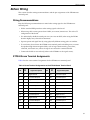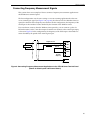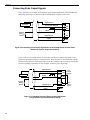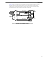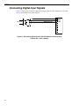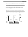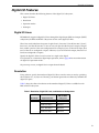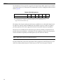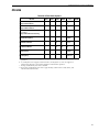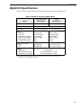
1
Title Page
UM-16862-N
DT340 User’s Manual
Copyright Page
Thirteenth Edition
January, 2010
Copyright © 1998 - 2010 by Data Translation, Inc.
All rights reserved.
Information furnished by Data Translation, Inc. is believed to be
accurate and reliable; however, no responsibility is assumed by
Data Translation, Inc. for its use; nor for any infringements of
patents or other rights of third parties which may result from its
use. No license is granted by implication or otherwise under any
patent rights of Data Translation, Inc.
Use, duplication, or disclosure by the United States Government
is subject to restrictions as set forth in subparagraph (c)(1)(ii) of
the Rights in Technical Data and Computer software clause at 48
C.F.R, 252.227-7013, or in subparagraph (c)(2) of the Commercial
Computer Software - Registered Rights clause at 48 C.F.R.,
52-227-19 as applicable. Data Translation, Inc., 100 Locke Drive,
Marlboro, MA 01752.
Data Translation, Inc.
100 Locke Drive
Marlboro, MA 01752-1192
(508) 481-3700
www.datatranslation.com
Fax: (508) 481-8620
E-mail: [email protected]
Data Translation® is a registered trademark of Data Translation,
Inc. DT-Open LayersTM, DT-Open Layers for .NET Class
LibraryTM, DataAcq SDKTM, Data Acquisition OMNI CDTM, LV
-LinkTM, and DTx-EZTM are trademarks of Data Translation, Inc.
All other brand and product names are trademarks or registered
trademarks of their respective companies.
FCC
Page
Radio and Television Interference
This equipment has been tested and found to comply with CISPR EN55022 Class A and
EN50082-1 (CE) requirements and also with the limits for a Class A digital device, pursuant to
Part 15 of the FCC Rules. These limits are designed to provide reasonable protection against
harmful interference when the equipment is operated in a commercial environment. This
equipment generates, uses, and can radiate radio frequency energy and, if not installed and
used in accordance with the instruction manual, may cause harmful interference to radio
communications. Operation of this equipment in a residential area is likely to cause harmful
interference, in which case the user will be required to correct the interference at his own
expense.
Changes or modifications to this equipment not expressly approved by Data Translation could
void your authority to operate the equipment under Part 15 of the FCC Rules.
Note: This product was verified to meet FCC requirements under test conditions that
included use of shielded cables and connectors between system components. It is important
that you use shielded cables and connectors to reduce the possibility of causing interference
to radio, television, and other electronic devices.
Canadian Department of Communications Statement
This digital apparatus does not exceed the Class A limits for radio noise emissions from
digital apparatus set out in the Radio Interference Regulations of the Canadian Department of
Communications.
Le présent appareil numérique n’émet pas de bruits radioélectriques dépassant les limites
applicables aux appareils numériques de la class A prescrites dans le Règlement sur le
brouillage radioélectrique édicté par le Ministère des Communications du Canada.
Table of Contents
Table of Contents
About this Manual . . . . . . . . . . . . . . . . . . . . . . . . . . . . . . . . . . . . . . . . . . . . . . . . . . . . . . 9
Intended Audience. . . . . . . . . . . . . . . . . . . . . . . . . . . . . . . . . . . . . . . . . . . . . . . . . . . . . . . . . . . . . 9
How this Manual is Organized . . . . . . . . . . . . . . . . . . . . . . . . . . . . . . . . . . . . . . . . . . . . . . . . . . 9
Conventions Used in this Manual . . . . . . . . . . . . . . . . . . . . . . . . . . . . . . . . . . . . . . . . . . . . . . . 10
Related Information . . . . . . . . . . . . . . . . . . . . . . . . . . . . . . . . . . . . . . . . . . . . . . . . . . . . . . . . . . . 10
Where To Get Help. . . . . . . . . . . . . . . . . . . . . . . . . . . . . . . . . . . . . . . . . . . . . . . . . . . . . . . . . . . . 11
Chapter 1: Overview . . . . . . . . . . . . . . . . . . . . . . . . . . . . . . . . . . . . . . . . . . . . . . . . . . . 13
Features . . . . . . . . . . . . . . . . . . . . . . . . . . . . . . . . . . . . . . . . . . . . . . . . . . . . . . . . . . . . . . . . . . . . . 14
Supported Software . . . . . . . . . . . . . . . . . . . . . . . . . . . . . . . . . . . . . . . . . . . . . . . . . . . . . . . . . . 15
Accessories . . . . . . . . . . . . . . . . . . . . . . . . . . . . . . . . . . . . . . . . . . . . . . . . . . . . . . . . . . . . . . . . . . 16
Getting Started Procedure. . . . . . . . . . . . . . . . . . . . . . . . . . . . . . . . . . . . . . . . . . . . . . . . . . . . . . 17
Part 1: Getting Started . . . . . . . . . . . . . . . . . . . . . . . . . . . . . . . . . . . . . 19
Chapter 2: Installing a DT340 Board and Loading the Device Driver . . . . . . . . . . . . 21
Unpacking . . . . . . . . . . . . . . . . . . . . . . . . . . . . . . . . . . . . . . . . . . . . . . . . . . . . . . . . . . . . . . . . . . 23
Setting up the Computer . . . . . . . . . . . . . . . . . . . . . . . . . . . . . . . . . . . . . . . . . . . . . . . . . . . . . . . 24
Setting up an Expansion Slot . . . . . . . . . . . . . . . . . . . . . . . . . . . . . . . . . . . . . . . . . . . . . . . . . . . 25
Configuring the DT340 Board . . . . . . . . . . . . . . . . . . . . . . . . . . . . . . . . . . . . . . . . . . . . . . . . . . 26
Inserting the Board into the Computer . . . . . . . . . . . . . . . . . . . . . . . . . . . . . . . . . . . . . . . . . . 28
Loading the Device Driver . . . . . . . . . . . . . . . . . . . . . . . . . . . . . . . . . . . . . . . . . . . . . . . . . . . . . 29
Windows XP. . . . . . . . . . . . . . . . . . . . . . . . . . . . . . . . . . . . . . . . . . . . . . . . . . . . . . . . . . . . . . 29
Windows Vista . . . . . . . . . . . . . . . . . . . . . . . . . . . . . . . . . . . . . . . . . . . . . . . . . . . . . . . . . . . . 29
Windows 7 . . . . . . . . . . . . . . . . . . . . . . . . . . . . . . . . . . . . . . . . . . . . . . . . . . . . . . . . . . . . . . . 30
Chapter 3: Attaching and Configuring the Screw Terminal Panel . . . . . . . . . . . . . . 31
Attaching the STP340 Screw Terminal Panel . . . . . . . . . . . . . . . . . . . . . . . . . . . . . . . . . . . . . . 33
Configuring the STP340 . . . . . . . . . . . . . . . . . . . . . . . . . . . . . . . . . . . . . . . . . . . . . . . . . . . . . . . 34
Chapter 4: Wiring Signals . . . . . . . . . . . . . . . . . . . . . . . . . . . . . . . . . . . . . . . . . . . . . . . 37
Before Wiring . . . . . . . . . . . . . . . . . . . . . . . . . . . . . . . . . . . . . . . . . . . . . . . . . . . . . . . . . . . . . . . . 39
Wiring Recommendations . . . . . . . . . . . . . . . . . . . . . . . . . . . . . . . . . . . . . . . . . . . . . . . . . . 39
STP340 Screw Terminal Assignments . . . . . . . . . . . . . . . . . . . . . . . . . . . . . . . . . . . . . . . . 39
Connecting Counter/Timer Signals . . . . . . . . . . . . . . . . . . . . . . . . . . . . . . . . . . . . . . . . . . . . . 41
Connecting Event Counting Signals . . . . . . . . . . . . . . . . . . . . . . . . . . . . . . . . . . . . . . . . . 41
Connecting Frequency Measurement Signals . . . . . . . . . . . . . . . . . . . . . . . . . . . . . . . . . 43
Connecting Pulse Output Signals . . . . . . . . . . . . . . . . . . . . . . . . . . . . . . . . . . . . . . . . . . . 44
Connecting Digital Input Signals . . . . . . . . . . . . . . . . . . . . . . . . . . . . . . . . . . . . . . . . . . . . . . . . 46
Connecting Digital Output Signals . . . . . . . . . . . . . . . . . . . . . . . . . . . . . . . . . . . . . . . . . . . . . . 47
5
Contents
Chapter 5: Verifying the Operation of a
DT340 Board . . . . . . . . . . . . . . . . . . . . . . . . . . . . . . . . . . . . . . . . . . . . . . . . . . . . . . . . . 49
Running the Quick DataAcq Application . . . . . . . . . . . . . . . . . . . . . . . . . . . . . . . . . . . . . . . . 51
Testing Single-Value Digital Input . . . . . . . . . . . . . . . . . . . . . . . . . . . . . . . . . . . . . . . . . . . . . . 52
Testing Single-Value Digital Output . . . . . . . . . . . . . . . . . . . . . . . . . . . . . . . . . . . . . . . . . . . . . 53
Testing Frequency Measurement . . . . . . . . . . . . . . . . . . . . . . . . . . . . . . . . . . . . . . . . . . . . . . . 54
Testing Pulse Output . . . . . . . . . . . . . . . . . . . . . . . . . . . . . . . . . . . . . . . . . . . . . . . . . . . . . . . . . . 55
Part 2: Using Your Board . . . . . . . . . . . . . . . . . . . . . . . . . . . . . . . . . . . 57
Chapter 6: Principles of Operation . . . . . . . . . . . . . . . . . . . . . . . . . . . . . . . . . . . . . . . 59
Counter/Timer Features . . . . . . . . . . . . . . . . . . . . . . . . . . . . . . . . . . . . . . . . . . . . . . . . . . . . . . . 61
Units . . . . . . . . . . . . . . . . . . . . . . . . . . . . . . . . . . . . . . . . . . . . . . . . . . . . . . . . . . . . . . . . . . . . 61
Clock Sources . . . . . . . . . . . . . . . . . . . . . . . . . . . . . . . . . . . . . . . . . . . . . . . . . . . . . . . . . . . . . 61
Internal C/T Clock . . . . . . . . . . . . . . . . . . . . . . . . . . . . . . . . . . . . . . . . . . . . . . . . . . . . 62
External C/T Clock . . . . . . . . . . . . . . . . . . . . . . . . . . . . . . . . . . . . . . . . . . . . . . . . . . . . 62
Internally Cascaded Clock . . . . . . . . . . . . . . . . . . . . . . . . . . . . . . . . . . . . . . . . . . . . . . 63
Gate Types . . . . . . . . . . . . . . . . . . . . . . . . . . . . . . . . . . . . . . . . . . . . . . . . . . . . . . . . . . . . . . . 63
Pulse Output Types and Duty Cycles . . . . . . . . . . . . . . . . . . . . . . . . . . . . . . . . . . . . . . . . 65
Interrupts . . . . . . . . . . . . . . . . . . . . . . . . . . . . . . . . . . . . . . . . . . . . . . . . . . . . . . . . . . . . . . . . 66
Operation Modes. . . . . . . . . . . . . . . . . . . . . . . . . . . . . . . . . . . . . . . . . . . . . . . . . . . . . . . . . . 66
Event Counting . . . . . . . . . . . . . . . . . . . . . . . . . . . . . . . . . . . . . . . . . . . . . . . . . . . . . . . 66
Frequency Measurement . . . . . . . . . . . . . . . . . . . . . . . . . . . . . . . . . . . . . . . . . . . . . . . 68
Rate Generation . . . . . . . . . . . . . . . . . . . . . . . . . . . . . . . . . . . . . . . . . . . . . . . . . . . . . . . 70
One-Shot . . . . . . . . . . . . . . . . . . . . . . . . . . . . . . . . . . . . . . . . . . . . . . . . . . . . . . . . . . . . . 72
Repetitive One-Shot . . . . . . . . . . . . . . . . . . . . . . . . . . . . . . . . . . . . . . . . . . . . . . . . . . . 74
Interval Timer Features . . . . . . . . . . . . . . . . . . . . . . . . . . . . . . . . . . . . . . . . . . . . . . . . . . . . . . . . 76
Units . . . . . . . . . . . . . . . . . . . . . . . . . . . . . . . . . . . . . . . . . . . . . . . . . . . . . . . . . . . . . . . . . . . . 76
Clock Sources . . . . . . . . . . . . . . . . . . . . . . . . . . . . . . . . . . . . . . . . . . . . . . . . . . . . . . . . . . . . . 76
Gate Types . . . . . . . . . . . . . . . . . . . . . . . . . . . . . . . . . . . . . . . . . . . . . . . . . . . . . . . . . . . . . . . 76
Pulse Output Types and Duty Cycles . . . . . . . . . . . . . . . . . . . . . . . . . . . . . . . . . . . . . . . . 76
Interrupts . . . . . . . . . . . . . . . . . . . . . . . . . . . . . . . . . . . . . . . . . . . . . . . . . . . . . . . . . . . . . . . . 76
Operation Modes. . . . . . . . . . . . . . . . . . . . . . . . . . . . . . . . . . . . . . . . . . . . . . . . . . . . . . . . . . 77
Digital I/O Features. . . . . . . . . . . . . . . . . . . . . . . . . . . . . . . . . . . . . . . . . . . . . . . . . . . . . . . . . . . 79
Digital I/O Lines . . . . . . . . . . . . . . . . . . . . . . . . . . . . . . . . . . . . . . . . . . . . . . . . . . . . . . . . . . 79
Resolution. . . . . . . . . . . . . . . . . . . . . . . . . . . . . . . . . . . . . . . . . . . . . . . . . . . . . . . . . . . . . . . . 79
Interrupts . . . . . . . . . . . . . . . . . . . . . . . . . . . . . . . . . . . . . . . . . . . . . . . . . . . . . . . . . . . . . . . . 80
Operation Modes. . . . . . . . . . . . . . . . . . . . . . . . . . . . . . . . . . . . . . . . . . . . . . . . . . . . . . . . . . 80
Chapter 7: Supported Device Driver Capabilities. . . . . . . . . . . . . . . . . . . . . . . . . . . . 83
Data Flow and Operation Options. . . . . . . . . . . . . . . . . . . . . . . . . . . . . . . . . . . . . . . . . . . . . . . 85
Buffering . . . . . . . . . . . . . . . . . . . . . . . . . . . . . . . . . . . . . . . . . . . . . . . . . . . . . . . . . . . . . . . . . . . . 86
6
Contents
Triggered Scan Mode . . . . . . . . . . . . . . . . . . . . . . . . . . . . . . . . . . . . . . . . . . . . . . . . . . . . . . . . . . 86
Data Encoding. . . . . . . . . . . . . . . . . . . . . . . . . . . . . . . . . . . . . . . . . . . . . . . . . . . . . . . . . . . . . . . . 86
Channels . . . . . . . . . . . . . . . . . . . . . . . . . . . . . . . . . . . . . . . . . . . . . . . . . . . . . . . . . . . . . . . . . . . . 87
Gain . . . . . . . . . . . . . . . . . . . . . . . . . . . . . . . . . . . . . . . . . . . . . . . . . . . . . . . . . . . . . . . . . . . . . . . . 87
Ranges . . . . . . . . . . . . . . . . . . . . . . . . . . . . . . . . . . . . . . . . . . . . . . . . . . . . . . . . . . . . . . . . . . . . . . 87
Resolution . . . . . . . . . . . . . . . . . . . . . . . . . . . . . . . . . . . . . . . . . . . . . . . . . . . . . . . . . . . . . . . . . . . 88
Thermocouple and RTD Support. . . . . . . . . . . . . . . . . . . . . . . . . . . . . . . . . . . . . . . . . . . . . . . . 89
IEPE Support. . . . . . . . . . . . . . . . . . . . . . . . . . . . . . . . . . . . . . . . . . . . . . . . . . . . . . . . . . . . . . . . . 89
Triggers . . . . . . . . . . . . . . . . . . . . . . . . . . . . . . . . . . . . . . . . . . . . . . . . . . . . . . . . . . . . . . . . . . . . . 90
Clocks . . . . . . . . . . . . . . . . . . . . . . . . . . . . . . . . . . . . . . . . . . . . . . . . . . . . . . . . . . . . . . . . . . . . . . . 91
Counter/Timers . . . . . . . . . . . . . . . . . . . . . . . . . . . . . . . . . . . . . . . . . . . . . . . . . . . . . . . . . . . . . . 92
Chapter 8: Troubleshooting . . . . . . . . . . . . . . . . . . . . . . . . . . . . . . . . . . . . . . . . . . . . . 95
General Checklist . . . . . . . . . . . . . . . . . . . . . . . . . . . . . . . . . . . . . . . . . . . . . . . . . . . . . . . . . . . . . 96
Technical Support . . . . . . . . . . . . . . . . . . . . . . . . . . . . . . . . . . . . . . . . . . . . . . . . . . . . . . . . . . . . . 98
If Your Board Needs Factory Service . . . . . . . . . . . . . . . . . . . . . . . . . . . . . . . . . . . . . . . . . . . . 99
Appendix A: Specifications . . . . . . . . . . . . . . . . . . . . . . . . . . . . . . . . . . . . . . . . . . . . 101
Counter/Timer Specifications . . . . . . . . . . . . . . . . . . . . . . . . . . . . . . . . . . . . . . . . . . . . . . . . . 102
Digital I/O Specifications . . . . . . . . . . . . . . . . . . . . . . . . . . . . . . . . . . . . . . . . . . . . . . . . . . . . . 103
Power, Physical, and Environmental Specifications . . . . . . . . . . . . . . . . . . . . . . . . . . . . . . . 104
Connector Specifications . . . . . . . . . . . . . . . . . . . . . . . . . . . . . . . . . . . . . . . . . . . . . . . . . . . . . . 105
Appendix B: Connector Pin Assignments . . . . . . . . . . . . . . . . . . . . . . . . . . . . . . . . 107
Connector J1 on the DT340 Board . . . . . . . . . . . . . . . . . . . . . . . . . . . . . . . . . . . . . . . . . . . . . . 108
Screw Terminal Assignments on the STP340 . . . . . . . . . . . . . . . . . . . . . . . . . . . . . . . . . . . . . 110
Screw Terminal Assignments for the STP68. . . . . . . . . . . . . . . . . . . . . . . . . . . . . . . . . . . . . . 112
Appendix C: Using Your Own Screw Terminal Panel . . . . . . . . . . . . . . . . . . . . . . . 115
Digital Inputs and Counter/Timer Inputs . . . . . . . . . . . . . . . . . . . . . . . . . . . . . . . . . . . . . . . 117
Digital Outputs . . . . . . . . . . . . . . . . . . . . . . . . . . . . . . . . . . . . . . . . . . . . . . . . . . . . . . . . . . . . . . 118
Cabling Information. . . . . . . . . . . . . . . . . . . . . . . . . . . . . . . . . . . . . . . . . . . . . . . . . . . . . . . . . . 119
Index . . . . . . . . . . . . . . . . . . . . . . . . . . . . . . . . . . . . . . . . . . . . . . . . . . . . . . . . . . . . . . . 121
7
Contents
8
About this Manual
This manual describes how to set up and install the following components:
• DT340 software
• DT340 board
• DT340 Device Driver
• STP340 screw terminal panel
It describes how to wire signals to the board and how to verify the board’s operation using the
Quick DataAcq application.
This manual also describes the features of the DT340 board, the capabilities of the DT340
Device Driver, and how to program the DT340 board using DT-Open Layers for .NET Class
Library™ software. Troubleshooting information is also provided.
Note: For information on checking system requirements, installing the software, and
viewing the documentation, refer to the README file on the OMNI CD.
For more information on the class library, refer to the DT-Open Layers for .NET Class Library
User’s Manual. If you are using the DataAcq SDK or a software application to program your
device, refer to the documentation for that software for more information.
Intended Audience
This document is intended for engineers, scientists, technicians, or others responsible for
using and/or programming a DT340 board for data acquisition operations in Microsoft®
Windows® XP, Windows Vista®, or Windows 7. It is assumed that you have some familiarity
with data acquisition principles, and that you understand your application.
How this Manual is Organized
This manual is organized as follows:
• Chapter 1, “Overview,” describes the major features of the board, as well as the supported
software and accessories for the board. It provides an overview of the DT340 getting
started procedure.
• Chapter 2, “Installing a DT340 Board and Loading the Device Driver,” describes how to
install the DT340 board and load the DT340 Device Driver.
• Chapter 3, “Attaching and Configuring the Screw Terminal Panel,” describes how to
configure the STP340 screw terminal panel.
• Chapter 4, “Wiring Signals,” describes how to wire signals to a DT340 board.
9
About this Manual
• Chapter 5, “Verifying the Operation of a DT340 Board,” describes how to verify the
operation of a DT340 board with the Quick DataAcq application
• Chapter 6, “Principles of Operation,” describes all of the board’s features and how to use
them in your application.
• Chapter 7, “Supported Device Driver Capabilities,” lists the data acquisition subsystems
and the associated features accessible using the DT340 Device Driver.
• Chapter 8, “Troubleshooting,” provides information that you can use to resolve problems
with the board and the device driver, should they occur.
• Appendix A, “Specifications,” lists the specifications of the board.
• Appendix B, “Connector Pin Assignments,” shows the pin assignments for the J1
connector on the DT340 board, on the STP340 screw terminal panel, and on the STP68
screw terminal panel.
• Appendix C, “Using Your Own Screw Terminal Panel,” describes additional
considerations to keep in mind when designing your own screw terminal panel for use
with a DT340 board.
• An index completes this manual.
Conventions Used in this Manual
The following conventions are used in this manual:
• Notes provide useful information or information that requires special emphasis, cautions
provide information to help you avoid losing data or damaging your equipment, and
warnings provide information to help you avoid catastrophic damage to yourself or your
equipment.
• Items that you select or type are shown in bold.
Related Information
Refer to the following documents for more information on using the DT340 board:
• Measure Foundry Manual (UM-19298) and online help. These documents describe how to
use Measure Foundry™ to build drag-and-drop test and measurement applications for
Data Translation® data acquisition devices.
• DT-Open Layers for .NET User’s Manual (UM-22161). For programmers who are
developing their own application programs using Visual C# or Visual Basic .NET, this
manual describes how to use the DT-Open Layers for .NET Class Library to access the
capabilities of Data Translation data acquisition devices.
• DataAcq SDK User’s Manual (UM-18326). For programmers who are developing their own
application programs using the Microsoft C compiler, this manual describes how to use
the DT-Open LayersTM Data Acq SDK to access the capabilities of Data Translation data
acquisition boards. This manual is included on the Data Acquisition OMNI CD.
• DTx-EZ Getting Started Manual (UM-15428). This manual describes how to use the ActiveX
controls provided in DTx-EZTM to access the capabilities of Data Translation data
acquisition boards in Microsoft® Visual BasicTM or Visual C++.
10
About this Manual
• LV-Link Online Help. This help file describes how to use LV-Link™ with the LabVIEW™
graphical programming language to access the capabilities of Data Translation data
acquisition devices.
• PCI Specification: PCI Local Bus Specification, PCI Special Interest Group, Portland, OR.
(Revision 2.1, June 1, 1995).
• Microsoft Windows XP, Windows Vista, or Windows 7 documentation.
Where To Get Help
Should you run into problems installing or using a DT340 board, our Technical Support
Department is available to provide prompt, technical assistance. Refer to Chapter 8 for more
information. If you are outside the U.S. or Canada, call your local distributor, whose number
is listed on our web site (www.datatranslation.com).
11
About this Manual
12
1
Overview
Features . . . . . . . . . . . . . . . . . . . . . . . . . . . . . . . . . . . . . . . . . . . . . . . . . . . . . . . . . . . . . . . . . . . . . 14
Supported Software . . . . . . . . . . . . . . . . . . . . . . . . . . . . . . . . . . . . . . . . . . . . . . . . . . . . . . . . . . . 15
Accessories . . . . . . . . . . . . . . . . . . . . . . . . . . . . . . . . . . . . . . . . . . . . . . . . . . . . . . . . . . . . . . . . . . 16
Getting Started Procedure. . . . . . . . . . . . . . . . . . . . . . . . . . . . . . . . . . . . . . . . . . . . . . . . . . . . . . 17
13
Chapter 1
Features
The DT340 is a low-cost counter/timer and digital I/O board for the PCI bus. The DT340
consists of the following major features:
• Eight 16-bit counter/timers programmable for event counting, frequency measurement,
rate generation (continuous pulse output), one-shot pulse output, and repetitive one-shot
pulse output
• Four 24-bit interval timers
• Interrupt capability for each counter/timer and interval timer (interrupts can be
individually enabled for the eight counter/timers, and are always enabled for the four
interval timers)
• Programmable gate types
• Programmable pulse output polarities (output types) and duty cycles
• Four 8-bit digital ports programmable as inputs or outputs on a per-port basis
• Digital outputs capable of driving external solid-state relays (15 mA)
• Change on interrupt capability for one 8-bit digital port
For a discussion of these features in detail, refer to Chapter 6 starting on page 59.
14
Overview
Supported Software
The following software is available for use with the DT340 board and is shipped on the Data
Acquisition OMNI CD:
• DT340 Device Driver – The device driver is installed automatically when you install the
software from the Data Acquisition OMNI CD. You need the device driver to use the
DT340 board with any of the supported software packages or utilities.
• The Quick DataAcq application – This application provides a quick way to get a DT340
board up and running. Using the Quick DataAcq application, you can verify the features
of the board, display data on the screen, and save data to disk.
• Measure Foundry – An evaluation version of this software is included on the Data
Acquisition OMNI CD. Measure Foundry is drag-and-drop test and measurement
application builder designed to give you top performance with ease-of-use development.
Order the full development version of this software package to develop your own
application using real hardware.
• DT-Open Layers for .NET Class Library – Use this class library if you want to use Visual
C# or Visual Basic for .NET to develop your own application software for the DT340 board
using Visual Studio 2003 or Visual Studio 2005; the class library complies with the
DT-Open Layers standard.
• DataAcq SDK – Use the Data Acq SDK if you want to use Visual Studio 6.0 and Microsoft
C or C++ to develop your own application software for the DT340 board using Windows
XP, Windows Vista, or Windows 7; the DataAcq SDK complies with the DT-Open Layers
standard.
• DTx-EZ – DTx-EZ provides ActiveX controls, which allow you to access the capabilities of
the DT340 boards using Microsoft Visual Basic or Visual C++; DTx-EZ complies with the
DT-Open Layers standard.
• LV-Link – An evaluation version of LV-Link is included on the Data Acquisition OMNI
CD. Use LV-Link if you want to use the LabVIEW graphical programming language to
access the capabilities of the DT340 boards.
Refer to the Data Translation web site (www.datatranslation.com) for information about
selecting the right software package for your needs.
15
Chapter 1
Accessories
The following optional accessories are available for the DT340 board:
• STP340 screw terminal panel – A screw terminal panel designed specifically for the
DT340 board, and used in the CE configuration of the board. It measures 3 15/16 inches
by 3 15/16 inches (100 mm x 100 mm), and has one connector to accommodate the
counter/timer and digital I/O signals provided by the DT340 board.
• STP68 screw terminal panel – A generic, 68-pin screw terminal panel that has one
connector to accommodate the counter/timer and digital I/O signals provided by the
DT340 board.
• EP305 cable – A 2-meter, twisted-pair, shielded cable that connects the 68-pin connector
(J1) on the DT340 board to the J1 connector on the STP340 or STP68 screw terminal panel.
• STP340 shielded box – A shielded box for use with the STP340 screw terminal panel. The
box measures 5.28 inches by 5.31 inches by 1.96 inches (134 mm x 135 mm x 50 mm). The
aluminum end plates measure 5.04 inches by 1.77 inches by 0.064 inches (128 mm x 45 mm
x 1.6 mm). The part number for the box is 1598RBGY (gray) or 1598RBBK (black). You can
purchase this box from Hammond Manufacturing directly, using the following
information:
Hammond Manufacturing Co, Ltd.
394 Edinburgh Road North
Guelph, Ontario N1H 1E5 Canada
Phone: (519) 822-2960 Canada; (716) 631-5700 USA
Web address: www.hammondmfg.com
16
Overview
Getting Started Procedure
The flow diagram shown in Figure 1 illustrates the steps needed to get started using a DT340
board. This diagram is repeated in each getting started chapter; the shaded area in the
diagram shows you where you are in the getting started procedure.
Install the Board and its Accessories
(see Chapter 2 starting on page 21)
Configure the Board and
Screw Terminal Panel
(see Chapter 3 starting on page 31)
Wire Signals
(see Chapter 4 starting on page 37)
Verify the Operation of the Board
(see Chapter 5 starting on page 49)
Figure 1: Getting Started Flow Diagram
17
Chapter 1
18
Part 1: Getting Started
2
Installing a DT340 Board and Loading the
Device Driver
Unpacking . . . . . . . . . . . . . . . . . . . . . . . . . . . . . . . . . . . . . . . . . . . . . . . . . . . . . . . . . . . . . . . . . . . 23
Setting up the Computer . . . . . . . . . . . . . . . . . . . . . . . . . . . . . . . . . . . . . . . . . . . . . . . . . . . . . . . 24
Setting up an Expansion Slot . . . . . . . . . . . . . . . . . . . . . . . . . . . . . . . . . . . . . . . . . . . . . . . . . . . 25
Configuring the DT340 Board . . . . . . . . . . . . . . . . . . . . . . . . . . . . . . . . . . . . . . . . . . . . . . . . . . 26
Inserting the Board into the Computer . . . . . . . . . . . . . . . . . . . . . . . . . . . . . . . . . . . . . . . . . . . 28
Loading the Device Driver . . . . . . . . . . . . . . . . . . . . . . . . . . . . . . . . . . . . . . . . . . . . . . . . . . . . . 29
21
Chapter 2
Install the Board and Load the Device
Driver (this chapter)
Attach and Configure the Screw Terminal
Panel (see Chapter 3 starting on page 31)
Wire Signals
(see Chapter 4 starting on page 37)
Verify the Operation of the Board
(see Chapter 5 starting on page 49)
Note: All DT340 boards are factory-calibrated and require no further adjustment prior to
installation.
22
Installing a DT340 Board and Loading the Device Driver
Unpacking
Open the shipping box and remove the wrapped DT340 board.
CAUTION:
Keep the board in its protective antistatic bag until you are ready to
install it; this minimizes the likelihood of electrostatic damage.
Verify that the following items are present:
• DT340 data acquisition board
• Data Acquisition OMNI CD
If an item is missing or damaged, contact Data Translation. If you are in the United States, call
the Customer Service Department at (508) 481-3700, ext 1323. An application engineer will
guide you through the appropriate steps for replacing missing or damaged items. If you are
located outside the United States, call your local distributor, listed on Data Translation’s web
site (www.datatranslation.com).
23
Chapter 2
Setting up the Computer
CAUTION:
To prevent electrostatic damage that can occur when handling
electronic equipment, use a ground strap or similar device when
performing this installation procedure.
To set up the computer, do the following:
1. Install the software from the Data Acquisition OMNI CD or Data Translation web site.
Note: If you are using Windows 7, you must install the device driver before installing the
board in the computer.
2. Turn off the computer.
3. Turn off all peripherals (printer, modem, monitor, and so on) connected to the computer.
4. Unplug the computer and all peripherals.
5. Remove the cover from you computer. Refer to your computer’s user manual for
instructions.
24
Installing a DT340 Board and Loading the Device Driver
Setting up an Expansion Slot
Once you have set up the computer, set up an expansion slot as follows:
1. Select a 32-bit or 64-bit PCI expansion slot.
PCI slots are shorter than ISA or EISA slots and are usually white or ivory. Commonly,
three PCI slots (one of which may be a shared ISA/PCI slot) are available. If an ISA board
exists in the shared slot, you cannot use the slot for a PCI board; if a PCI board exists in the
shared slot, you cannot use the slot for an ISA board.
2. Remove the cover plate from the selected expansion slot. Retain the screw that held it in
place; you will use it later to install the board.
25
Chapter 2
Configuring the DT340 Board
The DT340 board has eight resistor locations that correspond to the eight clock input signals
on the board. Figure 2 shows the location of the resistors on the DT340 board.
C/T 0
C/T 3
DT340 Board
C/T 4
C/T 7
Figure 2: User-Resistor Locations on the DT340 Board
Table 1 lists the clock input signals and the resistors to which they correspond.
Table 1: Clock Input Signals and Resistor Use
26
Clock Input Signal
Resistor
Clock Input 0
R1
Clock Input 1
R2
Clock Input 2
R3
Clock Input 3
R4
Clock Input 4
R5
Clock Input 5
R6
Clock Input 6
R7
Clock Input 7
R8
Installing a DT340 Board and Loading the Device Driver
If you are using high-frequency external clock input signals (greater than 1 MHz), do the
following:
1. Insert a resistor to ground for the corresponding counter/timer clock input signal on the
DT340 board. This resistor is used in parallel with the 1 kΩ resistor on the board. The
appropriate value for the user-supplied resistor depends on your application, the
frequency of the clock input signal, and the cable length.
Note: When using clock sources greater than 1 MHz, it is recommended that you use
counter/timers 0 to 3. This is the CE configuration of the board.
2. Terminate the corresponding signal on the STP340 panel by replacing the 0 Ω resistor on
the STP340 with a resistor of an appropriate matching value (page 34 for more
information).
For example, if you are connecting an external clock signal to clock input signal 0 on the
DT340 board and running the board at its maximum clock input frequency, it is recommended
that you insert a 110 Ω resistor to ground on the board for the clock input signal 0, and replace
the 0 Ω resistor in location R1 on the STP340 panel with a 100 Ω resistor for proper termination.
27
Chapter 2
Inserting the Board into the Computer
Once you have set up an expansion slot and configured the DT340 board, do the following to
insert the DT340 board into the computer:
1. Discharge any static electricity by holding the wrapped board in one hand while placing
your other hand firmly on a metal portion of the computer chassis.
2. Carefully remove the antistatic packing material from the board. (Save the original
packing material in the unlikely event that your board requires servicing in the future.)
3. Hold the board by its edges and do not touch any of the components on the board.
4. Position the board so that the cable connectors are facing the rear of the computer, as
shown in Figure 3.
DT340 Board
Rear of Computer
PCI Expansion Slot Bus Connector
Figure 3: Inserting the DT340 Board in the Computer
5. Carefully lower the board into the PCI expansion slot using the card guide to properly
align the board in the slot.
6. When the bottom of the board contacts the bus connector, gently press down on the board
until it clicks into place.
CAUTION:
Do not force the board into place. Moving the board from side to side
during installation may damage the bus connector. If you encounter
resistance when inserting the board, remove the board and try again.
7. Secure the board in place at the rear panel of the system unit using the screw removed
from the slot cover.
8. Power up the computer.
If you installed the DT340 software, the DT340 device driver is loaded automatically. If you have
not installed the software, do so now.
28
Installing a DT340 Board and Loading the Device Driver
Loading the Device Driver
To load the DT340 Device Driver in
• Windows XP, follow the steps on page 29.
• Windows Vista, follow the steps on page 29.
• Windows 7, follow the steps on page 30.
Windows XP
Once you have installed the software from the Data Acquisition OMNI CD, installed a DT340
board, and powered up the host computer, the New Hardware Found dialog box appears. Do
the following to load the device driver in Windows XP:
1. Click Next.
2. Click Search for a suitable driver for my device (recommended).
3. Click Specify a location, and click Next.
4. Browse to Windows\Inf\DT340.Inf, and then click Open.
5. Click OK.
6. Click Next.
The files are copied.
7. Click Finish.
8. Open the Control Panel.
9. Double-click the Open Layers Control Panel icon.
10. Select the DT340 board to configure, and then click Advanced.
11. Select the appropriate boxes to enable interrupts for lines (bits) 0 to 7 on digital port D,
user counter/timers 0 to 7, and interval timers 8 to 11.
12. When you are finished, click Close.
13. If you wish to change the name of the board, click Edit Name and enter a new name for
the board. Otherwise, exit from the Control Panel.
Once the driver is loaded, perform the steps in Chapter 3 to attach and configure the screw
terminal panel for use with the DT340 board.
Windows Vista
Once you have installed the software from the Data Acquisition OMNI CD, installed a DT340
board, and powered up the host computer, the New Hardware Found dialog box appears. Do
the following to load the device driver in Windows Vista:
1. Click Locate and install driver software (recommended).
The popup message "Windows needs your permission to continue" appears.
2. Click Continue.
The Windows Security dialog box appears.
29
Chapter 2
3. Click Install this driver software anyway.
The driver files are installed.
4. Open the Control Panel.
5. Double-click the Open Layers Control Panel icon.
6. Select the DT340 board to configure, and then click Advanced.
7. Select the appropriate boxes to enable interrupts for lines (bits) 0 to 7 on digital port D,
user counter/timers 0 to 7, and interval timers 8 to 11.
8. When you are finished, click Close.
9. If you wish to change the name of the board, click Edit Name and enter a new name for
the board. Otherwise, exit from the Control Panel.
Once the driver is loaded, perform the steps in Chapter 3 to attach and configure the screw
terminal panel for use with the DT340 board.
Windows 7
Once you have installed the software from the Data Acquisition OMNI CD, installed a DT340
board, and powered up the host computer, the hardware is found automatically. Perform the
following steps to configure the device driver.
1. Open the Control Panel.
2. Double-click the Open Layers Control Panel icon.
3. Select the DT340 board to configure, and then click Advanced.
4. Select the appropriate boxes to enable interrupts for lines (bits) 0 to 7 on digital port D,
user counter/timers 0 to 7, and interval timers 8 to 11.
5. When you are finished, click Close.
6. If you wish to change the name of the board, click Edit Name and enter a new name for
the board. Otherwise, exit from the Control Panel.
Once the driver is loaded, perform the steps in Chapter 3 to attach and configure the screw
terminal panel for use with the DT340 board.
30
3
Attaching and Configuring the Screw
Terminal Panel
Attaching the STP340 Screw Terminal Panel . . . . . . . . . . . . . . . . . . . . . . . . . . . . . . . . . . . . . . 33
Configuring the STP340. . . . . . . . . . . . . . . . . . . . . . . . . . . . . . . . . . . . . . . . . . . . . . . . . . . . . . . . 34
31
Chapter 3
Install the Board and Load the Device
Driver (see Chapter 2 starting on page 21)
Attach and Configure the Screw Terminal
Panel (this chapter)
Wire Signals
(see Chapter 4 starting on page 37)
Verify the Operation of the Board
(see Chapter 5 starting on page 49)
32
Attaching and Configuring the Screw Terminal Panel
Attaching the STP340 Screw Terminal Panel
Connector J1 on the screw terminal panel provides all of the digital and counter/timer signals
from connector J1 on the DT340 board. Cable EP305 connects connector J1 on the screw
terminal panel to the DT340 board.
Figure 4 illustrates how to attach the STP340 screw terminal panel to the DT340 board.
DT340
Board
J1
EP305 Cable
J1
STP340 Screw
Terminal Panel
Figure 4: Attaching the STP340 Screw Terminal Panel to the DT340 Board
33
Chapter 3
Configuring the STP340
The STP340 screw terminal panel has eight resistor locations which correspond to the eight
clock input signals. Figure 5 shows the location of the resistors on the STP340 screw terminal
panel.
J1, 68-Pin Connector
R5
R7
TB28
TB20
TB17
R8
R6
TB29
TB1
TB9
R4
TB24
TB32
TB4
TB12
TB25
R1
R3
R2
TB8
TB16
TB21
Resistor
Locations
TB13
TB5
TB63
TB53
TB43
TB33
TB72
TB62
TB52
TB42
Figure 5: Resistor Locations on the STP340 Screw Terminal Panel
Table 2 lists the clock input signals and the resistors to which they correspond.
Table 2: Clock Input Signals and Resistor Use
34
Clock Input Signal
Resistor
Clock Input 0
R1
Clock Input 1
R2
Clock Input 2
R3
Clock Input 3
R4
Clock Input 4
R5
Clock Input 5
R6
Clock Input 6
R7
Clock Input 7
R8
Attaching and Configuring the Screw Terminal Panel
By default, the STP340 is shipped with 0 Ω resistors in these resistor locations.
If you changed the resistor values on the board (), ensure that you terminate the
corresponding signal on the STP340 panel by replacing the 0 Ω resistor on the STP340 with a
resistor of an appropriate matching value.
For example, if you are connecting an external clock signal to clock input signal 0 on the
DT340 board and running the board at its maximum clock input frequency, it is
recommended that you insert a 110 Ω resistor to ground on the board for the clock input
signal 0, and replace the 0 Ω resistor in location R1 on the STP340 panel with a 100 Ω resistor
for proper termination.
35
Chapter 3
36
4
Wiring Signals
Before Wiring . . . . . . . . . . . . . . . . . . . . . . . . . . . . . . . . . . . . . . . . . . . . . . . . . . . . . . . . . . . . . . . . 39
Connecting Counter/Timer Signals . . . . . . . . . . . . . . . . . . . . . . . . . . . . . . . . . . . . . . . . . . . . . 41
Connecting Digital Input Signals. . . . . . . . . . . . . . . . . . . . . . . . . . . . . . . . . . . . . . . . . . . . . . . . 46
Connecting Digital Output Signals . . . . . . . . . . . . . . . . . . . . . . . . . . . . . . . . . . . . . . . . . . . . . . 47
37
Chapter 4
Install the Board and Load the Device Driver
(see Chapter 2 starting on page 21)
Attach and Configure the Screw Terminal
Panel (see Chapter 3 starting on page 31)
Wire Signals
(this chapter)
Verify the Operation of the Board
(see Chapter 5 starting on page 49)
This chapter describes how to wire signals to the STP340 screw terminal panel.
Note: If you are using a screw terminal panel other than the STP340, refer to page 115 for
additional wiring considerations.
38
Wiring Signals
Before Wiring
This section describes wiring recommendations and the pin assignments of the STP340 screw
terminal panel.
Wiring Recommendations
Keep the following recommendations in mind when wiring signals to the STP340 screw
terminal panel:
• Follow standard ESD procedures when wiring signals to the board.
• When using clock sources greater than 1 MHz, use counter/timers 0 to 3. This is the CE
configuration of the board.
• Use individually shielded twisted-pair wire (size 14 to 26 AWG) when using the DT340
board in highly noisy electrical environments.
• Separate power and signal lines by using physically different wiring paths or conduits.
• To avoid noise, do not locate the STP340 screw terminal panel and cabling next to sources
that produce high electro-magnetic fields, such as large electric motors, power lines,
solenoids, and electric arcs, unless the signals are enclosed in a mumetal shield.
• Connect the shields to one end only (either at the STP340 or at the signal source).
STP340 Screw Terminal Assignments
Table 3 lists the screw terminal assignments for the STP340 screw terminal panel.
Table 3: Screw Terminal Assignments on the STP340 Screw Terminal Panel
J1
Pin
TB
Signal Description
J1
Pin
TB
Signal Description
1
68
Digital Ground
2
67
C/T Clock Input 0
3
66
C/T Clock Output 0
4
65
C/T Gate Input 0
5
34
Digital Ground
6
33
C/T Clock Input 1
7
32
C/T Clock Output 1
8
31
C/T Gate Input 1
9
64
C/T Gate Input 2
10
63
C/T Clock Output 2
11
62
C/T Clock Input 2
12
61
Digital Ground
13
30
C/T Gate Input 3
14
29
C/T Clock Output 3
15
28
C/T Clock Input 3
16
27
Digital Ground
17
42
Digital Ground
18
41
C/T Clock Input 4
19
40
C/T Clock Output 4
20
39
C/T Gate Input 4
21
8
Digital Ground
22
7
C/T Clock Input 5
23
6
C/T Clock Output 5
24
5
C/T Gate Input 5
39
Chapter 4
Table 3: Screw Terminal Assignments on the STP340 Screw Terminal Panel (cont.)
J1
Pin
TB
40
Signal Description
J1
Pin
TB
Signal Description
25
38
C/T Gate Input 6
26
37
C/T Clock Output 6
27
36
C/T Clock Input 6
28
35
Power Ground
29
4
C/T Gate Input 7
30
3
C/T Clock Output 7
31
2
C/T Clock Input 7
32
1
+5 V Output
33
-
Shield
34
60
Digital I/O Port A, Line 0
35
26
Digital I/O Port A, Line 1
36
59
Digital I/O Port A, Line 2
37
25
Digital I/O Port A, Line 3
38
58
Digital I/O Port A, Line 4
39
24
Digital I/O Port A, Line 5
40
57
Digital I/O Port A, Line 6
41
23
Digital I/O Port A, Line 7
42
56
Digital Ground
43
-
Shield
44
55
Digital I/O Port B, Line 0
45
21
Digital I/O Port B, Line 1
46
54
Digital I/O Port B, Line 2
47
20
Digital I/O Port B, Line 3
48
53
Digital I/O Port B, Line 4
49
19
Digital I/O Port B, Line 5
50
52
Digital I/O Port B, Line 6
51
18
Digital I/O Port B, Line 7
52
22
Digital Ground
53
-
Shield
54
51
Digital I/O Port C, Line 0
55
17
Digital I/O Port C, Line 1
56
50
Digital I/O Port C, Line 2
57
16
Digital I/O Port C, Line 3
58
49
Digital I/O Port C, Line 4
59
15
Digital I/O Port C, Line 5
60
48
Digital I/O Port C, Line 6
61
14
Digital I/O Port C, Line 7
62
47
Digital Ground
63
-
Shield
64
46
Digital I/O Port D, Line 0
65
12
Digital I/O Port D, Line 1
66
45
Digital I/O Port D, Line 2
67
11
Digital I/O Port D, Line 3
68
44
Digital I/O Port D, Line 4
69
10
Digital I/O Port D, Line 5
70
43
Digital I/O Port D, Line 6
71
9
Digital I/O Port D, Line 7
72
13
Digital Ground
Wiring Signals
Connecting Counter/Timer Signals
The DT340 board with the STP340 screw terminal panel provides user counter/timers that
you can use to perform the following operations:
• Event counting
• Frequency measurement
• Pulse output (rate generation, one-shot, and repetitive one-shot)
Connecting Event Counting Signals
Figure 6 shows one example of connecting event counting signals to the STP340 screw
terminal panel using user counter 0. In this example, rising clock edges are counted while the
gate is active.
Digital Ground
User Clock Input 0
TB1
TB2
Signal Source
TB4
Gate 0
External
Gating
Switch
TB12
Digital Ground
Shield
TB33
STP340 Panel
Figure 6: Connecting Event Counting Applications to the STP340 Screw Terminal Panel
(Shown for Clock Input 0 and External Gate 0)
Figure 7 shows another example of connecting an event counting application to the STP340
screw terminal panel using user counter 0. In this example, a software gate is used to start the
event counting operation.
41
Chapter 4
Digital Ground
TB1
User Clock Input 0
TB2
Signal Source
Shield
TB33
STP340 Panel
Figure 7: Connecting Event Counting Applications to the STP340 Screw Terminal Panel
without an External Gate Input (Shown for Clock Input 0)
Figure 8 shows an example of how to externally cascade two counters to perform an event
counting operation using user counters 0 and 2. Note that you can also internally cascade
counters using software; if you internally cascade the counters, you do not have to make the
external cascading connections. Note also that this example shows the use of an external gate;
however, this connection is not required.
Digital Ground
TB1
TB2
User Clock Input 0
Signal Source
External
Gating
Switch
TB3
Gate 0
TB4
TB11
TB12
Digital Ground
Shield
TB33
STP340 Panel
Figure 8: Cascading Counters (Shown for Event Counting
Using Counters 0 and 2 and External Gate 0
42
User
Counter
Output 0
User
Clock
Input 2
Wiring Signals
Connecting Frequency Measurement Signals
This section shows two examples of how to connect a frequency measurement application to
the STP340 screw terminal panel.
The first configuration uses the same wiring as an event counting application that does not
use an external gate signal (see Figure 7 on page 42); the software uses the Windows timer to
specify the duration of the frequency measurement. In this configuration, the frequency of the
clock input is the number of counts divided by the duration of the Windows timer.
If you need more accuracy than the Windows timer provides, you can connect a pulse of a
known duration (such as a one-shot output of another user counter) to the external gate input,
as shown in Figure 9. In this configuration, the frequency of the clock input is the number of
counts divided by the period of the external gate input.
Digital Ground
User Clock Input 0
TB1
TB2
Signal Source
Gate 0
TB4
TB10
User
Counter
Output 2
Shield
TB33
STP340 Panel
Figure 9: Connecting Frequency Measurement Applications to the STP340 Screw Terminal Panel
(Shown for Clock Input 0 and External Gate 0)
43
Chapter 4
Connecting Pulse Output Signals
Figure 10 shows one example of connecting a pulse output application to the STP340 screw
terminal panel using user counter 0. Other combinations of signals can be used.
Heater
Controller
Digital Ground
TB1
User Counter Output 0
TB3
TB4
Gate 0
External
Gating
Switch
Digital Ground
TB12
Shield
TB33
STP340 Panel
Figure 10: Connecting Pulse Output Applications to the STP340 Screw Terminal Panel
(Shown for Counter Output 0 and Gate 0)
Figure 11 shows an example of how to externally cascade two counters to perform a rate
generation operation using user counters 0 and 2. Note that you can also internally cascade
counters using software; if you internally cascade the counters, you do not have to make the
external cascading connections. In this example, counter 2 gate is logic high.
Digital Ground
TB1
TB2
User Clock Input 0
Signal Source
External
Gating
Switch
Gate 0
TB3
TB4
TB11
Digital Ground
Shield
TB12
TB33
STP340 Panel
Figure 11: Cascading Counters (Shown for Rate Generation
Using Counters 0 and 2 and External Gate 0)
44
User
Counter
Output 0
User
Clock
Input 2
Wiring Signals
Figure 12 shows an example of how to externally cascade two counters to perform a one-shot
operation using user counters 0 and 2. Note that you can also internally cascade counters
using software; if you internally cascade the counters, you do not have to make the external
cascading connections. In this example, counter 0 gate is logic high.
Digital Ground
TB1
TB2
User Clock Input 0
Signal Source
User
Counter
Output 0
TB3
TB4
TB9
Gate 2
One-Shot
Trigger
TB11
TB12
Digital Ground
Shield
User
Clock
Input 2
TB33
STP340 Panel
Figure 12: Cascading Counters (Shown for One-Shot Using
Counters 0 and 2 and External Gate 2)
45
Chapter 4
Connecting Digital Input Signals
Figure 13 shows how to connect a digital input signal (lines 0 and 1 of digital Port A, in this
case) to the STP340 screw terminal panel.
Shield
TTL Inputs
Digital I/O Port A 0
Digital I/O Port A 1
TB33
TB34
TB35
STP340 Panel
Figure 13: Connecting Digital Inputs to the STP340 Screw Terminal Panel
(Lines 0 and 1, Port A Shown)
46
Wiring Signals
Connecting Digital Output Signals
Figure 14 shows how to connect a digital output signal (line 0 of digital Port B, in this case) to
the STP340 screw terminal panel.
0 Out = LED On
500
Ω
TB44
Digital I/O Port B 0
+
5V
Digital Ground
TB52
STP340 Panel
Figure 14: Connecting Digital Outputs to the STP340 Screw Terminal Panel
(Line 0, Port B Shown)
47
Chapter 4
48
5
Verifying the Operation of a
DT340 Board
Running the Quick DataAcq Application. . . . . . . . . . . . . . . . . . . . . . . . . . . . . . . . . . . . . . . . . 51
Testing Single-Value Digital Input . . . . . . . . . . . . . . . . . . . . . . . . . . . . . . . . . . . . . . . . . . . . . . . 52
Testing Single-Value Digital Output . . . . . . . . . . . . . . . . . . . . . . . . . . . . . . . . . . . . . . . . . . . . . 53
Testing Frequency Measurement . . . . . . . . . . . . . . . . . . . . . . . . . . . . . . . . . . . . . . . . . . . . . . . . 54
Testing Pulse Output . . . . . . . . . . . . . . . . . . . . . . . . . . . . . . . . . . . . . . . . . . . . . . . . . . . . . . . . . . 55
49
Chapter 5
Install the Board and Load the Device
Driver (see Chapter 2 starting on page 21)
Attach and Configure the Screw Terminal
Panel (see Chapter 3 starting on page 31)
Wire Signals
(see Chapter 4 starting on page 37)
Verify the Operation of the Board
(this chapter)
You can verify the operation of a DT340 board using the Quick DataAcq application. Quick
DataAcq lets you do the following:
• Acquire data from a single digital input port
• Measure the frequency of events
• Output data from a single analog output channel or digital output port
• Output pulses either continuously or as a one-shot
This chapter describes how to run the Quick DataAcq application.
50
Verifying the Operation of a DT340 Board
Running the Quick DataAcq Application
The Quick DataAcq application is installed automatically when you install the driver
software.
To run the Quick DataAcq application, do the following:
1. If you have not already done so, power up your computer and any attached peripherals.
2. Click Start from the Task Bar.
3. Browse to Programs|Data Translation, Inc| DT-Open Layers for
Win32|QuickDataAcq.
The main menu appears.
Note: The Quick DataAcq application allows you to verify basic operations on the board;
however, it may not support all of the board’s features.
For information on each of the features provided, use the online help for the Quick DataAcq
application by pressing F1 from any view or selecting the Help menu. If the system has
trouble finding the help file, navigate to C:\Program Files\Data Translation\Win32\
dtdataacq.hlp, where C: is the letter of your hard disk drive.
51
Chapter 5
Testing Single-Value Digital Input
To verify that the board can read a single digital input value, do the following:
1. Connect a digital input to digital input line 0 of port A on the DT340 board. Refer to page
46 for an example of how to connect a digital input.
2. In the Quick DataAcq application, choose Digital Input from the Acquisition menu.
3. Select the appropriate DT340 board from the Board list box.
4. Select digital input port A by clicking Port A.
5. Click Get.
The application displays the value of each digital input line in port A on the screen in both text and
graphical form.
52
Verifying the Operation of a DT340 Board
Testing Single-Value Digital Output
To verify that the board can output a single digital output value, perform the following steps:
1. Connect a digital output to digital output line 0 of port B on the DT340 board. Refer to
page 47 for an example of how to connect a digital output.
2. In the Quick DataAcq application, choose Digital Output from the Control menu.
3. Select the appropriate DT340 board from the Board list box.
4. Select digital output port B by clicking Port B.
5. Click the appropriate bits to select the digital output lines to write to. If the bit is selected,
a high-level signal is output to the digital output line; if the bit is not selected, a low-level
signal is output to the digital output line. Optionally, you can enter an output value in the
Hex text box.
6. Click Send.
The application displays the value of each digital output line of digital port B on the screen in both
text and graphical form.
53
Chapter 5
Testing Frequency Measurement
To verify that the board can perform a frequency measurement operation, do the following:
1. Wire an external clock source to counter/timer 0 on the DT340 board. Refer to page 43 for
an example of how to connect a an external clock for a frequency measurement operation.
Note: The Quick DataAcq application works only with counter/timer 0.
2. In the Quick DataAcq application, choose Frequency Counter from the Acquisition
menu.
3. Select the appropriate DT340 board from the Board list box.
4. In the Count Duration text box, enter the number of seconds during which events will be
counted.
5. Click Start to start the frequency measurement operation.
The operation automatically stops after the number of seconds you specified has elapsed, and the
application displays the frequency on the screen.
If you want to stop the frequency measurement operation when it is in progress, click Stop.
54
Verifying the Operation of a DT340 Board
Testing Pulse Output
To verify that the board can perform a pulse output operation, do the following:
1. Connect a scope to counter/timer 0 on the DT340 board. Refer to page 44 for an example
of how to connect a scope (a pulse output) to counter/timer 0.
Note: The Quick DataAcq application works only with counter/timer 0.
2. In the Quick DataAcq application, choose Pulse Generator from the Control menu.
3. Select the appropriate DT340 board from the Board list box.
4. Select either Continuous to output a continuous pulse stream or One Shot to output one
pulse.
5. Select either Low-to-high to output a rising-edge pulse (the high portion of the total pulse
output period is the active portion of the signal) or High-to-low to output a falling-edge
pulse (the low portion of the total pulse output period is the active portion of the signal).
6. Enter a percentage or use the slider to select a percentage for the pulse width. The pulse
width determines the duty cycle of the pulse.
7. Click Start to generate the pulse(s).
The application displays the results both in text and graphical form.
8. Click Stop to stop a continuous pulse output operation. One-shot pulse output operations
stop automatically.
55
Chapter 5
56
Part 2: Using Your Board
6
Principles of Operation
Counter/Timer Features . . . . . . . . . . . . . . . . . . . . . . . . . . . . . . . . . . . . . . . . . . . . . . . . . . . . . . . 61
Interval Timer Features . . . . . . . . . . . . . . . . . . . . . . . . . . . . . . . . . . . . . . . . . . . . . . . . . . . . . . . . 76
Digital I/O Features. . . . . . . . . . . . . . . . . . . . . . . . . . . . . . . . . . . . . . . . . . . . . . . . . . . . . . . . . . . 79
59
Chapter 6
This chapter describes the counter/timer and digital I/O features of the DT340 board. To
frame the discussions, refer to the block diagram shown in Figure 15. Note that bold entries
indicate signals you can access.
C/T Clk [7:4]
C/T Gate [7:4]
C/T Out [7:4]
DIO Port D
In and Out
Registers
DIO Port D
[7:0]
8
DIO Port C
In and Out
Registers
DIO Port C
[7:0]
8
DIO Port B
In and Out
Registers
DIO Port B
[7:0]
8
DIO Port A
In and Out
Registers
DIO Port A
[7:0]
Counter/Timer 1
4 Counter/Timers
(16 bits each)
-----------------------2 Interval Timers
(24 bits each)
C/T Clk [3:0]
Counter/Timer 0
C/T Gate [3:0]
4 Counter/Timers
(16 bits each)
-----------------------2 Interval Timers
(24 bits each)
C/T Out [3:0]
8
16
I/T Out [3:2]
16
I/T Out [1:0]
C/T Out [7:0]
I/T Out [3:0]
Interrupt
Generator
DIO Port D [7:0]
LD[15:0]
PCI Bus Interface
PCI Bus
Figure 15: Block Diagram of the DT340 Board
60
Principles of Operation
Counter/Timer Features
This section describes the following user counter/timer features:
• Units
• Clock sources
• Gate types
• Pulse types and duty cycles
• Operation modes
Units
DT340 boards support eight 16-bit user counter/timer units (numbered 0 to 7). Each unit
accepts a clock input signal and gate input signal, and outputs a clock output signal (also
called a pulse output signal), as shown in Figure 16.
Clock Input SIgnal
(internal, external, or
internally cascaded)
Counter/Timer Unit
Clock Output Signal
Gate Input Signal
(software or external
input)
Figure 16: Counter/Timers
Each counter/timer unit corresponds to a counter/timer (C/T) subsystem. To select the unit
to use in software, specify the corresponding C/T subsystem. For example, to select
counter/timer 0, specify C/T subsystem element 0; to select counter/timer 7, specify C/T
subsystem element 7.
Clock Sources
The following clock sources are available for the counter/timers:
• Internal C/T clock
• External C/T clock
• Internally cascaded clock
Refer to the following subsections for more information on these clock sources.
61
Chapter 6
Note: When using clock sources greater than 1 MHz, it is recommended that you use
counter/timers 0 to 3. This is the CE configuration of the board.
Internal C/T Clock
The internal C/T clock uses a 40 MHz time base. Counter/timer operations start on the rising
edge of the clock input signal.
Through software, specify the clock source as internal and the frequency at which to pace the
counter/timer operation (this is the frequency of the clock output signal). Using the internal
clock source, the maximum frequency that you can specify for the clock output signal is 20
MHz. The minimum frequency that you can specify for the clock output signal is 610 Hz.
External C/T Clock
The external C/T clock is useful when you want to pace counter/timer operations at rates not
available with the internal C/T clock, or if you want to pace at uneven intervals. The rising
edge of the external C/T clock input signal is the active edge.
Using software, specify the clock source as external and the clock divider used to determine
the frequency at which to pace the operation (this is the frequency of the clock output signal).
The minimum clock divider that you can specify is 2.0; the maximum clock divider that you
can specify is 65,536. For example, assume that you want to generate a continuous rate and
you supplied an external C/T clock with a frequency of 5 MHz. If you specify a clock divider
of 5, the resulting frequency of the external C/T clock output signal is 1 MHz.
You can use an external C/T clock source with an input frequency of up to 20 MHz; however,
the resulting frequency of the external C/T clock output signal must not exceed 10 MHz.
Connect the external C/T clock to the board through the STP340 screw terminal panel. Table 4
lists the screw terminals that correspond to the external C/T clock signals of each
counter/timer.
Table 4: External C/T Clock Signals
62
Counter/Timer
Screw Terminal on
STP340
Pin on
Connector J1
0
TB2
67
1
TB6
33
2
TB11
62
3
TB15
28
4
TB18
41
Principles of Operation
Table 4: External C/T Clock Signals (cont.)
Counter/Timer
Screw Terminal on
STP340
Pin on
Connector J1
5
TB22
7
6
TB27
36
7
TB31
2
Internally Cascaded Clock
You can also internally route the clock output signal from one counter/timer to the clock input
signal of the next counter/timer to internally cascade the counter/timers. In this way, you can
create a 32-bit counter/timer without externally connecting two counter/timers together.
DT340 boards support internal (software) cascading on the following counter/timers:
• 0 and 1
• 1 and 2
• 2 and 3
• 4 and 5
• 5 and 6
• 6 and 7
Specify internal cascade mode in software. The rising edge of the clock input signal is active.
Through software, specify the clock source as internal and the frequency at which to pace the
counter/timer operation (this is the frequency of the clock output signal). The maximum
frequency that you can specify for the clock output signal is 10 MHz. For a 32-bit cascaded
counter, the minimum frequency that you can specify for the clock output signal is 0.00931 Hz,
which corresponds to a rate of once every 107 seconds.
Note: In software, specify the clock input and gate input for the first counter/timer in the
cascaded pair. For example, if counter/timers 1 and 2 are cascaded, specify the clock input
and gate input for counter/timer 1.
Gate Types
The active edge or level of the gate input to the counter enables counter/timer operations. The
operation starts when the clock input signal is received. DT340 boards provide the following
gate input types:
• None – A software command enables any specified counter/timer operation immediately
after execution. This gate type is useful for all counter/timer modes.
63
Chapter 6
• Logic-low level external gate input – Enables a counter/timer operation when the
external gate signal is low, and disables the counter/timer operation when the external
gate signal is high. Note that this gate type is used only for event counting, frequency
measurement, and rate generation; refer to page 66 for more information on these modes.
• Logic-high level external gate input – Enables a counter/timer operation when the
external gate signal is high, and disables a counter/timer operation when the external
gate signal is low. Note that this gate type is used only for event counting, frequency
measurement, and rate generation; refer to page 66 for more information on these modes.
• Falling-edge external gate input – Enables a counter/timer operation on the transition
from the high level to the low level (falling edge). In software, this is called a low-edge
gate type. Note that this gate type is used only for one-shot and repetitive one-shot mode;
refer to page 66 for more information on these modes.
• Rising-edge external gate input – Enables a counter/timer operation on the transition
from the low level to the high level (rising edge). In software, this is called a high-edge
gate type. Note that this gate type is used only for one-shot and repetitive one-shot mode;
refer to page 66 for more information on these modes.
Specify the gate type in software.
Table 5 lists the screw terminals that correspond to the gate input signals of each
counter/timer.
Table 5: Gate Input Signals
64
Counter/Timer
Screw Terminal on
STP340
Pin on
Connector J1
0
TB4
65
1
TB8
31
2
TB9
64
3
TB13
30
4
TB20
39
5
TB24
5
6
TB25
38
7
TB29
4
Principles of Operation
Pulse Output Types and Duty Cycles
DT340 boards can output pulses from each user counter/timer.
Table 6 lists the screw terminals that correspond to the pulse output signals of each
counter/timer.
Table 6: Pulse Output Signals
Counter/Timer
Screw Terminal on
STP340
Pin on
Connector J1
0
TB3
66
1
TB7
32
2
TB10
63
3
TB14
29
4
TB19
40
5
TB23
6
6
TB26
37
7
TB30
3
DT340 boards support the following pulse output types on the clock output signal:
• High-to-low transitions – The low portion of the total pulse output period is the active
portion of the counter/timer clock output signal.
• Low-to-high transitions – The high portion of the total pulse output period is the active
portion of the counter/timer pulse output signal.
You specify the pulse output type in software.
The duty cycle (or pulse width) indicates the percentage of the total pulse output period that is
active. A duty cycle of 50, then, indicates that half of the total pulse is low and half of the total
pulse output is high. You specify the duty cycle in software.
Figure 17 illustrates a low-to-high pulse with a duty cycle of approximately 30%.
Active Pulse Width
high
low
Total Pulse Period
Figure 17: Example of a Low-to-High Pulse Output Type
65
Chapter 6
Interrupts
You can use any of the eight user counter/timers to generate an interrupt to the host
computer. You enable the interrupts during DT340 driver configuration. The interrupt occurs
when the pulse output of the counter/timer changes from a low to a high state.
In a typical pulse output application where you want an interrupt to occur, it is recommended
that you specify the pulse output type as high-to-low. When the pulse output changes from a
low to high state (based on the frequency and duty cycle of the pulse), the interrupt occurs. If
the pulse output type is low-to-high, you can use the duty cycle to generate an interrupt
whenever the pulse output changes from a low to high state.
In a typical event counting application where you want an interrupt to occur, the pulse output
falls sometime before the terminal count is reached, then rises when the counter rolls over
from the terminal count to the initial count. The terminal count is 216 for a non-cascaded
counter/timer or 232 for a cascaded counter/timer.
In a typical event notification application where you want an interrupt to occur after a
specified number of external events has occurred, use an external clock and specify an
external clock divider. In this case, the value for the external clock divider determines the
number of events that are counted before an interrupt is generated.
Operation Modes
DT340 boards support the following counter/timer operation modes:
• Event counting
• Frequency measurement
• Rate generation
• One-shot
• Repetitive one-shot
The following subsections describe these modes in more detail.
Event Counting
Use event counting mode to count events from the counter’s external clock input source.
If you are using one counter/timer, you can count a maximum of 65,536 events before the
counter rolls over to 0 and starts counting again. If you are using a cascaded 32-bit counter,
you can count a maximum of 4,294,967,296 events before the counter rolls over to 0 and starts
counting again.
Note: If interrupts are enabled for a C/T subsystem operating in event counting mode, the
interrupt occurs when the maximum number of counts is reached (before the counter rolls
over to 0). An event is generated with the interrupt occurs.
66
Principles of Operation
In event counting mode, use an external C/T clock source; refer to page 61 for more
information on the external C/T clock source.
Note: An external clock divider is not used when counting events.
Using software, specify the counter/timer mode as event counting (count), the C/T clock
source as external, and the gate type that enables the operation. Refer to page 63 for
information on gates.
Ensure that the signals are wired appropriately. Figure 18 shows one example of connecting
an event counting application to the STP340 screw terminal panel using user counter 0. In this
example, rising clock edges are counted while the gate is active.
Digital Ground
User Clock Input 0
TB1
TB2
Signal Source
TB4
Gate 0
External
Gating
Switch
Digital Ground
TB12
TB33
Shield
STP340 Panel
Figure 18: Connecting Event Counting Signals
(Shown for Clock Input 0 and External Gate 0)
Figure 19 shows an example of an event counting operation. In this example, the gate type is
low level.
67
Chapter 6
high level
disables operation
Gate Input
Signal
low level
enables operation
External C/T
Clock
Input Signal
3 events are counted while
the operation is enabled
event counting
operation stops
event counting
operation starts
Figure 19: Example of Event Counting
Frequency Measurement
Use frequency measurement mode to measure the frequency of the signal from counter’s
external clock input source over a specified duration. In this mode, use an external C/T clock
source; refer to page 61 for more information on the external C/T clock source.
One way to perform a frequency measurement is to use the same wiring as an event counting
application that does not use an external gate signal, as shown in Figure 20.
Digital Ground
User Clock Input 0
TB1
TB2
Signal Source
Shield
TB33
STP340 Panel
Figure 20: Connecting Frequency Measurement Signals without
an External Gate Input (Shown for Clock Input 0)
68
Principles of Operation
In this configuration, use software to specify the counter/timer mode as frequency
measurement or event counting, and the duration of the Windows timer over which to
measure the frequency. (The Windows timer uses a resolution of 1 ms.) In this configuration,
frequency is determined using the following equation:
Frequency Measurement =
Number of Events
Duration of the Windows Timer
If you need more accuracy than the Windows timer provides, you can connect a pulse of a
known duration (such as a one-shot output of another counter/timer) to the external gate
input, as shown in
Figure 21.
Digital Ground
TB1
TB2
User Clock Input 0
Signal Source
TB4
Gate 0
TB10
User
Counter
Output 2
Shield
TB33
STP340 Panel
Figure 21: Connecting Frequency Measurement Signals
(Shown for Clock Input 0 and External Gate 0)
In this configuration, use software to set up the counter/timers as follows:
1. Set up one of the counter/timers for one-shot mode, specifying the clock source, clock
frequency, gate type, and type of output pulse (high or low).
2. Set up the counter/timer that will measure the frequency for event counting mode,
specifying the clock source to count, and the gate type (this should match the pulse output
type of the counter/timer set up for one-shot mode).
3. Start both counters (events are not counted until the active period of the one-shot pulse is
generated).
4. Read the number of events counted. (Allow enough time to ensure that the active period
of the one-shot occurred and that events have been counted.)
5. Determine the measurement period using the following equation:
Measurement period =
1
* Active Pulse Width
Clock Frequency
69
Chapter 6
6. Determine the frequency of the clock input signal using the following equation:
Frequency Measurement =
Number of Events
Measurement Period
Figure 22 shows an example of a frequency measurement operation. In this example, three
events are counted during a duration of 300 ms. The frequency, then, is 10 Hz, since 10 Hz =
3/(.3 s).
3 Events Counted
External C/T
Clock
Input Signal
Duration over which the
frequency is measured = 300 ms
frequency measurement
starts
frequency measurement
stops
Figure 22: Example of Frequency Measurement
Rate Generation
Use rate generation mode to generate a continuous pulse output signal from the counter; this
mode is sometimes referred to as continuous pulse output or pulse train output. You can use
this pulse output signal as an external clock to pace other operations.
While the pulse output operation is enabled, the counter outputs a pulse of the specified type
and frequency continuously. As soon as the operation is disabled, rate generation stops.
Note: If interrupts are enabled for a C/T subsystem operating in rate generation mode, the
interrupt occurs when the pulse output signal changes from a low to a high state. An event is
generated when the interrupt occurs.
The period of the output pulse is determined by the clock input signal and the external clock
divider. If you are using one counter (not cascaded), you can output pulses using a maximum
frequency of 20 MHz (this is the frequency of the clock output signal). In rate generation
mode, either the internal or external C/T clock input source is appropriate depending on your
application; refer to page 61 for more information on the C/T clock source.
70
Principles of Operation
Using software, specify the counter/timer mode as rate generation (rate), the C/T clock
source as either internal or external, the polarity of the output pulses (high-to-low transitions
or low-to-high transitions), the duty cycle of the output pulses, and the gate type that enables
the operation. Refer to page 65 for more information on pulse output signals and to page 63
for more information on gate types.
Note: If you want to use interrupts, we recommend that you specify the output pulse type
as high to low. The interrupt occurs when the output pulse completes.
For rate generation operations, use a duty cycle as close to 100% as possible to output a pulse
immediately. Using a duty cycle closer to 0% acts as a pulse output delay.
Ensure that the signals are wired appropriately. Figure 23 shows one example of connecting a
pulse output operation to the STP340 screw terminal panel using user counter 0. In this
example, a software gate type is used.
Digital Ground
Signal
Source
User Timer Input 0
TB1
User Timer Output 0
TB2
TB3
Heater
Controller
TB12
Digital Ground
STP340 Panel
Figure 23: Connecting Rate Generation Signals
(Shown for Counter Output 0; a Software Gate is Used)
Figure 24 shows an example of an enabled rate generation operation using an external C/T
clock source with an input frequency of 4 kHz, a clock divider of 4, a high-to-low pulse type,
and a duty cycle of 75%. (The gate type does not matter for this example.) A 1 kHz square
wave is the generated output. Figure 25 shows the same example using a duty cycle of 25%.
71
Chapter 6
If enabled,
interrupt occurs.
Rate Generation
Operation Starts
If enabled,
interrupt occurs.
External C/T
Clock
Input Signal
(4 kHz)
Pulse
Output
Signal
75% duty cycle
Figure 24: Example of Rate Generation Mode with a 75% Duty Cycle
Continuous Pulse
Output Operation Starts
If enabled,
interrupt occurs.
If enabled,
interrupt occurs.
External C/T
Clock
Input Signal
(4 kHz)
Pulse
Output
Signal
25% duty cycle
Figure 25: Example of Rate Generation Mode with a 25% Duty Cycle
One-Shot
Use one-shot mode to generate a single pulse output signal from the counter when the
operation is triggered (determined by the gate input signal). You can use this pulse output
signal as an external gate to start other operations.
When the one-shot operation is triggered, a single pulse is output; then, the one-shot
operation stops. All subsequent clock input signals and gate input signals are ignored.
72
Principles of Operation
Note: If interrupts are enabled for a C/T subsystem operating in one-shot mode, the
interrupt occurs when the pulse output signal changes from a low to a high state. An event is
generated when the interrupt occurs.
The period of the output pulse is determined by the clock input signal. In one-shot mode,
generally the internal C/T clock source is more useful than an external C/T clock source.
However, if you want to be notified after a number of external events occurs, specify an
external clock source; in this case, the external clock divider specifies the number of events
that occur before the interrupt is generated. Refer to page 61 for more information on the C/T
clock sources.
Using software, specify the counter/timer mode as one-shot, the clock source, the frequency
of the output signal or the number of events that occur before the interrupt, the polarity of the
output pulse (high-to-low transition or low-to-high transition), and the gate type to trigger the
operation. Refer to page 65 for more information on pulse output types and to page 63 for
more information on gate types.
Note: If you want to use interrupts, we recommend that you specify the output pulse type
as high to low. The interrupt occurs when the one-shot pulse completes. An event is
generated when the interrupt occurs.
In the case of a one-shot operation, the pulse width is automatically set to 100%.
Ensure that the signals are wired appropriately. Figure 26 shows one example of connecting a
pulse output operation to the STP340 screw terminal panel using user counter 0.
Digital Ground
Heater
Controller
TB1
C/T Output 0
External
Gating
Switch
Gate 0
Digital Ground
TB3
TB4
TB12
STP340 Panel
Figure 26: Connecting One-Shot Signals
(Shown for Counter Output 0 and Gate 0)
73
Chapter 6
Figure 27 shows an example of a one-shot operation using an external gate input (rising edge),
a clock output frequency of 1 kHz (pulse period of 1 ms), and a high-to-low pulse type.
One-Shot Operation
Starts
If enabled,
interrupt occurs.
External
Gate
Signal
1 ms period
100% duty cycle
Pulse
Output
Signal
Figure 27: Example of One-Shot Mode
Repetitive One-Shot
Use repetitive one-shot mode to generate a pulse output signal each time the board detects a
trigger (determined by the gate input signal). You can use this mode to clean up a poor clock
input signal by changing its pulse width, then outputting it.
Note: If interrupts are enabled for a C/T subsystem operating in repetitive one-shot mode,
the interrupt occurs each time the pulse output signal changes from a low to a high state. An
event is generated when the interrupt occurs.
The period of the output pulse is determined by the clock input signal. In one-shot mode,
generally the internal C/T clock source is more useful than an external C/T clock source.
However, if you want to be notified after a number of external events occurs, specify an
external clock source; in this case, the external clock divider specifies the number of events
that occur before the interrupt is generated. Refer to page 61 for more information on the C/T
clock sources.
Use software to specify the counter/timer mode as repetitive one-shot, the C/T clock source,
the frequency of the output signal or that number of events that occur before the interrupt, the
polarity of the output pulses (high-to-low transitions or low-to-high transitions), and the gate
type to trigger the operation. Refer to page 65 for more information on pulse output types and
to page 63 for more information on gates.
74
Principles of Operation
Note: If you want to use interrupts, we recommend that you specify the output pulse type
as high to low. The interrupt occurs when each one-shot pulse completes.
In the case of a repetitive one-shot operation, the pulse width is automatically set to 100%.
When the one-shot operation is triggered (determined by the gate input signal), a pulse is
output. When the board detects the next trigger, another pulse is output. This operation
continues until you stop the operation.
Note: Triggers that occur while the pulse is being output are not detected by the board.
Figure 28 shows an example of a repetitive one-shot operation using an external gate (rising
edge); a clock output frequency of 1 kHz (one pulse every 1 ms), and a high-to-low pulse type.
Repetitive One-Shot
Operation Starts
If enabled,
interrupt occurs.
If enabled,
interrupt occurs.
External
Gate
Signal
1 ms period
Pulse
Output
Signal
99.99% duty cycle
1 ms period
99.99% duty cycle
99.99%
duty cycle
Figure 28: Example of Repetitive One-Shot Mode
75
Chapter 6
Interval Timer Features
This section describes the following user interval timer features:
• Units
• Clock sources
• Gate types
• Pulse types and duty cycles
• Operation modes
Units
DT340 boards support four 24-bit interval timer units (numbered 8
to 11).
Interval timers use an internal clock input signal and internal gate input signal, and generate
an internal clock output signal. No external connections are supported.
Each interval timer corresponds to a counter/timer (C/T) subsystem. Select the interval timer
to use in software by specifying its corresponding C/T subsystem. For example, to select
interval timer 9, specify C/T subsystem 9.
Clock Sources
Interval timers are clocked by the internal 40 MHz clock. In software, specify the clock source
as internal. Specify the frequency of the interval timer from 2.39 Hz to 20 MHz.
Gate Types
For interval timers, use software to specify the gate type as none (software). Only a software
gate can enable an interval timer operation.
Pulse Output Types and Duty Cycles
For interval timer operations, the DT340 board generates a clock output signal that the board
uses internally to generate an interrupt condition; it is not brought out for user connection.
The pulse output type is high-to-low; it is not programmable. The pulse output signal is active
(low) for one clock pulse (25 ns); the duty cycle (pulse width) is not programmable.
Interrupts
Each of the four interval timers can generate a periodic interrupt to the host computer on each
low-to-high transition of the pulse output signal. Interrupts are always enabled for interval
timers. The interrupt frequency is equal to the frequency of the internal clock source.
76
Principles of Operation
Operation Modes
To generate an interrupt using an interval timer, set up the interval timer as follows in
software:
• Specify the interval timer for one-shot or rate generation mode. In one-shot mode, a single
interrupt is generated after the first pulse output changes from a low to a high state. In
rate generation mode, a interrupt occurs every time the pulse output changes from a low
to a high state.
• Specify the interval timer clock source as internal and the frequency of the clock source.
The period of the output pulse (the interval) is 1/clock frequency. Refer to page 76 for
more information on the interval timer clock source.
• Specify the gate type as none (software).
Figure 29 shows an example of an interval timer set up for one-shot mode, using a software
gate, and a clock frequency of 1 kHz (one pulse every 1 ms).
One-Shot Operation
Starts
Interrupt is Generated
1 ms period
Internal
Pulse
Output
Signal
25 ns
25 ns
Figure 29: Example of an Interval Timer Operation Using One-Shot Mode
Figure 30 shows an example of an interval timer set up for rate generation mode, using a
software gate, and a clock frequency of 1 kHz (one pulse every 1 ms).
77
Chapter 6
Rate Generation
Operation Starts
Interrupt is Generated
1 ms period
1 ms period
Internal
Pulse
Output
Signal
Interrupt is Generated
25 ns
25 ns
Figure 30: Example of an Interval Timer Operation Using Rate Generation Mode
78
Principles of Operation
Digital I/O Features
This section describes the following features of the digital I/O subsystem:
• Digital I/O lines
• Resolution
• Operation modes
• Interrupts
Digital I/O Lines
DT340 boards support 32 digital I/O lines through the digital input (DIN) and output (DOUT)
subsystems; the DIN and DOUT subsystems use the same digital I/O lines.
These lines are divided into four ports of eight: Port A, lines 0 to 7; Port B, lines 0 to 7; Port C,
lines 0 to 7; and Port D, lines 0 to 7. You can use each port for either input or output; all eight
lines within a port have the same configuration. For example, if you use Port A for input, lines
0 to 7 of Port A are configured as inputs. Likewise, if you use Port B for output, lines 0 to 7 of
Port B are configured as outputs.
Specify the digital I/O line to read or write in a single-value digital
I/O operation or a continuous digital input operation; refer to page 80 for more information
on digital I/O operation modes.
On power up or reset, no digital data is output from the board.
Resolution
Using software, specify the number of digital I/O lines to read or write at once by specifying
the resolution as 8, 16, 24, or 32. Choosing a resolution greater than 8 effectively combines the
digital I/O ports.
Table 7 shows the effect of resolution on the number of digital I/O lines available for each
DIN or DOUT subsystem.
Table 7: Resolution, Digital I/O Lines, and Number of Subsystems
Resolution
8
Digital I/O Lines
DIN or DOUT
Subsystem
Port A, lines 0 to 7
Element 0
Port B, lines 0 to 7
Element 1
Port C, lines 0 to 7
Element 2
Port D, lines 0 to 7
Element 3
79
Chapter 6
Table 7: Resolution, Digital I/O Lines, and Number of Subsystems
Resolution
16
Digital I/O Lines
DIN or DOUT
Subsystem
Port A and B, lines 0 to
15 combined
Element 0
Port C and D, lines 0 to
15 combined
Element 2
24
Port A, B, and C, lines
0 to 23 combined
Element 0
32
Ports A, B, C, and D,
lines 0 to 31 combined
Element 0
Note: When the resolution is greater than 8, the bit value represents the combined number
of digital I/O lines. For example, if the resolution is 32, digital I/O lines 0 to 7 of Port A are
represented as bits 0 to 7 of the digital value, digital I/O lines 0 to 7 of Port B are represented
as bits 8 to 15 of the digital value, digital I/O lines 0 to 7 of Port C are represented as bits 16 to
23 of the digital value, and digital I/O lines 0 to 7 of Port D are represented as bits 24 to 31 of
the digital value.
Interrupts
The DT340 board can generate a PCI-bus interrupt when any of the eight digital input lines
corresponding to digital Port D (DIN element 3) changes state. This feature is useful when you
want to monitor critical signals or when you want to signal the host computer to transfer data
to or from the board. You enable the interrupts on a line-by-line basis during DT340 driver
configuration; refer to page 29 for more information.
In software, an event is generated when the interrupt occurs. Use software to determine which
digital line changed state; refer to page 81 for more information.
Operation Modes
DT340 boards support the following digital I/O operation modes:
• Single-value operations are the simplest to use but do not allow you to check the
interrupt status. Use software to specify the DIN or DOUT subsystem, and the resolution
of the subsystem. Data is then read from or written to the appropriate digital I/O lines.
For a single-value operation, you cannot specify a clock or trigger source.
Single-value operations stop automatically when finished; you cannot stop a single-value
operation.
80
Principles of Operation
• Continuous digital input allows you to read digital input values as well as check the
interrupt status of digital Port D only.
Use software to specify DIN subsystem element 3, continuous mode, a resolution of 8, and
the trigger source as software. Once the operation is configured and started, an event is
generated when the interrupt occurs. You can then read the value and determine which
digital I/O line changed state to cause the interrupt.
Note: If you are using the DataAcq SDK to perform a continuous digital input operation,
use the lParam parameter of the olDaSetWndHandle or olDaSetNotificationProcedure
function to determine which digital input line changed state and the status of the digital
input port when the interrupt occurred.
The low word of lParam contains the digital lines (bits) that changed state, where bit 0
corresponds to digital input line 0 and bit 7 corresponds to digital input line 0.
The high word of lParam contains the state of the digital input subsystem, where the bits
represent the digital input lines.
The resolution reflects the number of significant bits in lParam.
81
Chapter 6
82
7
Supported Device Driver Capabilities
Data Flow and Operation Options. . . . . . . . . . . . . . . . . . . . . . . . . . . . . . . . . . . . . . . . . . . . . . . 85
Buffering . . . . . . . . . . . . . . . . . . . . . . . . . . . . . . . . . . . . . . . . . . . . . . . . . . . . . . . . . . . . . . . . . . . . 86
Triggered Scan Mode . . . . . . . . . . . . . . . . . . . . . . . . . . . . . . . . . . . . . . . . . . . . . . . . . . . . . . . . . . 86
Gain . . . . . . . . . . . . . . . . . . . . . . . . . . . . . . . . . . . . . . . . . . . . . . . . . . . . . . . . . . . . . . . . . . . . . . . . 87
Channels . . . . . . . . . . . . . . . . . . . . . . . . . . . . . . . . . . . . . . . . . . . . . . . . . . . . . . . . . . . . . . . . . . . . 87
Ranges . . . . . . . . . . . . . . . . . . . . . . . . . . . . . . . . . . . . . . . . . . . . . . . . . . . . . . . . . . . . . . . . . . . . . . 87
Resolution . . . . . . . . . . . . . . . . . . . . . . . . . . . . . . . . . . . . . . . . . . . . . . . . . . . . . . . . . . . . . . . . . . . 88
Thermocouple and RTD Support. . . . . . . . . . . . . . . . . . . . . . . . . . . . . . . . . . . . . . . . . . . . . . . . 89
IEPE Support. . . . . . . . . . . . . . . . . . . . . . . . . . . . . . . . . . . . . . . . . . . . . . . . . . . . . . . . . . . . . . . . . 89
Triggers . . . . . . . . . . . . . . . . . . . . . . . . . . . . . . . . . . . . . . . . . . . . . . . . . . . . . . . . . . . . . . . . . . . . . 90
Clocks . . . . . . . . . . . . . . . . . . . . . . . . . . . . . . . . . . . . . . . . . . . . . . . . . . . . . . . . . . . . . . . . . . . . . . . 91
Counter/Timers . . . . . . . . . . . . . . . . . . . . . . . . . . . . . . . . . . . . . . . . . . . . . . . . . . . . . . . . . . . . . . 92
83
Chapter 7
The DT340 Device Driver provides support for the digital input (DIN), digital output (DOUT),
and counter/timer (C/T) subsystems. For information on how to configure the device driver,
refer to page 29.
Table 8: DT340 Subsystems
DT340
Total Subsystems on Board
A/D
0
D/A
0
DIN
4a
DOUT
4a
C/T
12b
QUAD
0
a. DIN and DOUT subsystems use the same DIO lines.
b. C/T subsystems 0 to 7 support counter/timer features only. C/T subsystems 8 to 11
support interval timer features only.
The tables in this chapter summarize the features available for use with the DT-Open Layers
for .NET Class Library and the DT340 board. The DT-Open Layers for .NET Class Library
provides properties that return support information for specified subsystem capabilities.
The first row in each table lists the subsystem types. The first column in each table lists all
possible subsystem capabilities. A description of each capability is followed by the property
used to describe that capability in the DT-Open Layers for .NET Class Library.
Note: Blank fields represent unsupported options.
For more information, refer to the description of these properties in the DT-Open Layers for
.NET Class Library online help or DT-Open Layers for .NET Class Library User’s Manual.
84
Supported Device Driver Capabilities
Data Flow and Operation Options
Table 9: DT340 Data Flow and Operation Options
DT340
Single-Value Operation Support
SupportsSingleValue
A/D
D/A
DIN
Yes
DOUT
C/T
QUAD
Yes
Simultaneous Single-Value Output
Operations
SupportsSetSingleValues
Continuous Operation Support
SupportsContinuous
Yesa
Yes
Continuous Operation until Trigger
SupportsContinuousPreTrigger
Continuous Operation before & after Trigger
SupportsContinuousPrePostTrigger
Waveform Operations Using FIFO Only
SupportsWaveformModeOnly
Simultaneous Start List Support
SupportsSimultaneousStart
Supports Programmable Synchronization
Modes
SupportsSynchronization
Synchronization Modes
SynchronizationMode
Interrupt Support
SupportsInterruptOnChange
Yesa
Output FIFO Size
FifoSize
Auto-Calibrate Support
SupportsAutoCalibrate
a. Only Port D when configured for 8-bit resolution can operate in continuous digital input mode
and only if you enabled interrupt usage for this port in the driver configuration dialog box. The
driver posts an event done message when a digital line in this port changes state. Refer to page
29 for more information on configuring the driver. If you are using the DataAcq SDK, refer to
page 80 for more information on determining which digital input lines changed state.
85
Chapter 7
Buffering
Table 10: DT340 Buffering Options
DT340
A/D
D/A
DIN
DOUT
C/T
QUAD
Buffer Support
SupportsBuffering
Single Buffer Wrap Mode Support
SupportsWrapSingle
Inprocess Buffer Flush Support
SupportsInProcessFlush
Triggered Scan Mode
Table 11: DT340 Triggered Scan Mode Options
DT340
A/D
D/A
DIN
DOUT
C/T
QUAD
Triggered Scan Support
SupportsTriggeredScan
Maximum Number of CGL Scans per Trigger
MaxMultiScanCount
0
0
0
Maximum Retrigger Frequency
MaxRetriggerFreq
0
0
0
Minimum Retrigger Frequency
MinRetriggerFreq
0
0
0
Data Encoding
Table 12: DT340 Data Encoding Options
DT340
Binary Encoding Support
SupportsBinaryEncoding
Twos Complement Support
SupportsTwosCompEncoding
Returns Floating-Point Values
ReturnsFloats
86
A/D
D/A
DIN
Yes
DOUT
Yes
C/T
Yes
QUAD
Supported Device Driver Capabilities
Channels
Table 13: DT340 Channel Options
DT340
A/D
D/A
Number of Channels
NumberOfChannels
DIN
DOUT
C/T
1
1
1
SE Channels
MaxSingleEndedChannels
0
0
0
DI Support
SupportsDifferential
Yes
Yes
Yes
DI Channels
MaxDifferentialChannels
1
1
1
Maximum Channel-Gain List Depth
CGLDepth
0
0
0
QUAD
SE Support
SupportsSingleEnded
Simultaneous Sample-and-Hold Support
SupportsSimultaneousSampleHold
Channel-List Inhibit
SupportsChannelListInhibit
Gain
Table 14: DT340 Gain Options
DT340
A/D
D/A
DIN
DOUT
C/T
QUAD
C/T
QUAD
Programmable Gain Support
SupportsProgrammableGain
Number of Gains
NumberOfSupportedGains
1
1
Gains Available
SupportedGains
1
1
0
Ranges
Table 15: DT340 Range Options
DT340
Number of Voltage Ranges
NumberOfRanges
A/D
D/A
DIN
0
DOUT
0
0
Available Ranges
SupportedVoltageRanges
Current Output Support
SupportsCurrentOutput
87
Chapter 7
Resolution
Table 16: DT340 Resolution Options
DT340
A/D
D/A
DIN
DOUT
C/T
Software Programmable Resolution
SupportsSoftwareResolution
Yesa
Yesa
Number of Resolutions
NumberOfResolutions
4a
4a
1
Available Resolutions
SupportedResolutions
8, 16,
24, 32a
8, 16,
24, 32a
16b
QUAD
a. When configured for 8 bits of resolution, element 0 uses bits 7 to 0 (Port A), element 1 uses
bits 15 to 8 (Port B), element 2 uses bits 23 to 16 (Port C), and element 3 uses bits 31 to 24 (Port
D). When configured for 16 bits of resolution, element 0 uses bits 15 to 0 (Ports A and B), and
element 2 uses bits 31 to 15 (Ports C and D). When configured for 24 bits of resolution,
element 0 uses bits 23 to 0 (Ports A, B, and C). When configured for 32 bits of resolution,
element 0 uses DIO bits 31 to 0 (Ports A, B, C, and D).
b. You can also cascade two 16-bit counter/timers together to create a 32-bit counter/timer.
88
Supported Device Driver Capabilities
Thermocouple and RTD Support
Table 17: DT340 Thermocouple and RTD Support Options
DT340
A/D
D/A
DIN DOUT C/T QUAD
Thermocouple Support
SupportsThernocouple
RTD Support
SupportsRTD
Resistance Support
ReturnsOhms
Voltage Converted to Temperature in Hardware
SupportsTemperatureDataInStream
Supported Thermocouple Types
ThermocoupleType
Supported RTD Types
RTDType
Supports CJC Source Internally in Hardware
SupportsCjcSourceInternal
Supports CJC Channel
SupportsCjcSourceChannel
Available CJC Channels
CjcChannel
Supports Interleaved CJC Values in Data Stream
SupportsInterleavedCjcTemperaturesInStream
Supports Programmable Filters
SupportsTemperatureFilters
Programmable Filter Types
TemperatureFilterType
IEPE Support
Table 18: DT340 IEPE Support Options
DT340
A/D
D/A
DIN
DOUT
C/T
QUAD
Software Programmable AC Coupling
SupportsACCoupling
Software Programmable DC Coupling
SupportsDCCoupling
Software Programmable External Excitation
Current Source
SupportsExternalExcitationCurrentSrc
Software Programmable Internal Excitation
Current Source
SupportsInternalExcitationCurrentSrc
Available Excitation Current Source Values
SupportedExcitationCurrentValues
89
Chapter 7
Triggers
Table 19: DT340 Trigger Options
DT340
Software Trigger Support
SupportsSoftwareTrigger
External Positive TTL Trigger Support
SupportsPosExternalTTLTrigger
External Negative TTL Trigger Support
SupportsNegExternalTTLTrigger
External Positive TTL Trigger Support for
Single-Value Operations
SupportsSvPosExternalTTLTrigger
External Negative TTL Trigger Support
for Single-Value Operations
SupportsSvNegExternalTTLTrigger
Positive Threshold Trigger Support
SupportsPosThresholdTrigger
Negative Threshold Trigger Support
SupportsNegThresholdTrigger
Digital Event Trigger Support
SupportsDigitalEventTrigger
90
A/D
D/A
DIN
DOUT
C/T
QUAD
Supported Device Driver Capabilities
Clocks
Table 20: DT340 Clock Options
DT340
A/D
D/A
DIN
DOUT
C/T
Internal Clock Support
SupportsInternalClock
Yesa
External Clock Support
SupportsExternalClock
Yesb
QUAD
Simultaneous Input/Output on a Single
Clock Signal
SupportsSimultaneousClocking
Base Clock Frequency
BaseClockFrequency
0
0
40 MHz
Maximum Clock Divider
MaxExtClockDivider
1.0
1,0
65536
Minimum Clock Divider
MinExtClockDivider
1.0
1.0
2.0
Maximum Frequency
MaxFrequency
0
0
20 MHzc
Minimum Frequency
MinFrequency
0
0
0.009 Hzd
a. An internal clock source is not supported for event counting and frequency measurement
operations.
b. C/T subsystems 0 to 7 support an external clock. C/T subsystems 8 to 11 do not support an
external clock; the clock source must be internal for interval timer operations.
c. If using cascaded timers, this value is 10 MHz.
d. If not using cascaded timers, this value is approximately 610 Hz for the counter/timers, and
2.39 Hz for the interval timers.
91
Chapter 7
Counter/Timers
Table 21: DT340 Counter/Timer Options
DT340
A/D
D/A
DIN
DOUT
C/T
Cascading Support
SupportsCascading
Yesa
Event Count Mode Support
SupportsCount
Yesb,c
Generate Rate Mode Support
SupportsRateGenerate
Yesb
One-Shot Mode Support
SupportsOneShot
Yes
Repetitive One-Shot Mode Support
SupportsOneShotRepeat
Yes
Up/Down Counting Mode Support
SupportsUpDown
Edge-to-Edge Measurement Mode Support
SupportsMeasure
Continuous Edge-to-Edge Measurement
Mode Support
SupportsContinuousMeasure
High to Low Output Pulse Support
SupportsHighToLowPulse
Yesd
Low to High Output Pulse Support
SupportsLowToHighPulse
Yesd
Variable Pulse Width Support
SupportsVariablePulseWidth
Yese
None (internal) Gate Type Support
SupportsGateNone
Yes
High Level Gate Type Support
SupportsGateHighLevel
Yesf,g
Low Level Gate Type Support
SupportsGateLowLevel
Yesf,g
High Edge Gate Type Support
SupportsGateHighEdge
Yesf,g
Low Edge Gate Type Support
SupportsGateLowEdge
Yesf,g
Level Change Gate Type Support
SupportsGateLevel
Clock-Falling Edge Type
SupportsClockFalling
Clock-Rising Edge Type
SupportsClockRising
Gate-Falling Edge Type
SupportsGateFalling
92
QUAD
Supported Device Driver Capabilities
Table 21: DT340 Counter/Timer Options (cont.)
DT340
A/D
D/A
DIN
DOUT
C/T
QUAD
Gate-Rising Edge Type
SupportsGateRising
Interrupt-Driven Operations
SupportsInterrupt
Yes
a. Only C/T subsystems 0 to 7 support internal cascading. The following adjacent counter/timers
can be cascaded in software: 0 and 1, 1 and 2, 2 and 3, 4 and 5, 5 and 6, and 6 and 7.
b. Only C/T subsystems 0 to 7 support this mode.
c. An external clock divider is not support for event counting operations.
d. Only C/T subsystems 0 to 7 support this pulse output type. The pulse output type is not
programmable for interval timers (C/T subsystems 8 to 11).
e. Interval timers (C/T subsystems 8 to 11) do not support programmable pulse widths.
f. For C/T subsystems 0 to 7, high-edge and low-edge are supported for one-shot and repetitive
one-shot modes only; high-level and low-level are supported for event counting and rate
generation modes only.
g. C/T subsystems 8 to 11 support a software (none) gate type only.
93
Chapter 7
94
8
Troubleshooting
General Checklist . . . . . . . . . . . . . . . . . . . . . . . . . . . . . . . . . . . . . . . . . . . . . . . . . . . . . . . . . . . . . 96
Technical Support . . . . . . . . . . . . . . . . . . . . . . . . . . . . . . . . . . . . . . . . . . . . . . . . . . . . . . . . . . . . . 98
If Your Board Needs Factory Service. . . . . . . . . . . . . . . . . . . . . . . . . . . . . . . . . . . . . . . . . . . . . 99
95
Chapter 8
General Checklist
Should you experience problems using the DT340 board, follow these steps:
1. Read all the documentation provided for your product. Make sure that you have added
any “Read This First” information to your manual and that you have used this
information.
2. Check the OMNI CD for any README files and ensure that you have used the latest
installation and configuration information available.
3. Check that your system meets the requirements stated in
the README file on the OMNI CD.
4. Check that you have installed your hardware properly using the instructions in Chapter
2.
5. Check that you have installed and configured the device driver properly using the
instructions in Chapter 2.
6. Search the DT Knowledgebase in the Support section of the Data Translation web site (at
www.datatranslation.com) for an answer to your problem.
If you still experience problems, try using the information in Table 22 to isolate and solve the
problem. If you cannot identify the problem, refer to page 98.
Table 22: Troubleshooting Problems
Symptom
Board does
not respond.
Possible Cause
Possible Solution
The board configuration is incorrect.
Check the configuration of your device driver to ensure
that the board name and type are correct.
The board is incorrectly aligned in a
PCI expansion slot.
Check that the slot in which your DT340 board is located is
a PCI slot and that the board is correctly seated in the slot.
The board is damaged.
Contact Data Translation for technical support; refer to
page 98.
The interrupt level is unacceptable.
An interrupt conflict exists in your system. The most
common interrupt conflict occurs with a PCI device and a
device that is plugged into the ISA bus. To resolve this
problem, change the interrupt setting (usually by changing
a jumper) on the ISA device.
An interrupt conflict can also occur if a PCI device was not
designed to share interrupts. To resolve this problem,
select a different interrupt for each PCI slot in the PCI
BIOS. To do this, enter the system BIOS program; this is
usually done by pressing the DEL key when rebooting your
system. Once in the system BIOS, enter the PCI/PnP
BIOS setup, and select a unique interrupt for each PCI
slot. The PCI BIOS assigns the interrupt; the device on the
PCI bus does not have control over the interrupt
assignment.
96
Troubleshooting
Table 22: Troubleshooting Problems (cont.)
Symptom
Possible Cause
Possible Solution
Board does
not respond
(cont.)
The interrupt level is unacceptable
(cont.)
Some network devices do not share interrupts. If you still
have an interrupt conflict, try removing the network device,
installing the DT340 board and rebooting the system, then
reinserting the network device.
Intermittent
operation.
Loose connections or vibrations exist.
Check your wiring and tighten any loose connections or
cushion vibration sources.
The board is overheating.
Check environmental and ambient temperature; consult
the board’s specifications on page 104 of this manual and
the documentation provided by your computer
manufacturer for more information.
Electrical noise exists.
Check your wiring and either provide better shielding or
reroute unshielded wiring.
Data appears
to be invalid.
An open connection exists.
Check your wiring and fix any open connections.
Computer
does not boot.
Board is not seated properly.
Check that the slot in which your DT340 board is located is
a PCI slot, that the board is correctly seated in the slot, and
that the board is secured in the slot with a screw.
The power supply of the computer is
too small to handle all the system
resources.
Check the power requirements of your system resources
and, if needed, get a larger power supply; consult the
board’s specifications on page 104 of this manual.
Board does
not interrupt.
Counter/timer, interval timer, or digital
I/O port is not configured properly.
Check the properties of the device driver configuration
using the instructions in Chapter 2.
System
lockup.
Board is not seated properly.
Check that the slot in which your DT340 board is located is
a PCI slot, that the board is correctly seated in the slot, and
that the board is secured in the slot with a screw.
An interrupt conflict exists in your system. The most
common interrupt conflict occurs with a PCI device and a
device that is plugged into the ISA bus. To correct this
problem, change the interrupt setting (usually by changing
a jumper) on the ISA device.
Interrupt level is unacceptable.
An interrupt conflict can also occur if a PCI device was not
designed to share interrupts. To resolve this problem,
select a different interrupt for each PCI slot in the PCI
BIOS. To do this, enter the system BIOS program; this is
usually done by pressing the DEL key when rebooting your
system. Once in the system BIOS, enter the PCI/PnP
BIOS setup, and select a unique interrupt for each PCI
slot. The PCI BIOS assigns the interrupt; the device on the
PCI bus does not have control over the interrupt
assignment.
Some network devices do not share interrupts. If you still
have an interrupt conflict, try removing the network device,
installing the DT340 board and rebooting the system, then
reinserting the network device.
Test button
grayed out.
Vdtdad VxD is not installed.
Load the DT340 Support Software or the Data Acq SDK.
97
Chapter 8
Technical Support
If you have difficulty using a DT340 board, Data Translation’s Technical Support Department
is available to provide technical assistance.
To request technical support, go to our web site at http://www.datatranslation.com and click
on the Support link.
When requesting technical support, be prepared to provide the following information:
• Your product serial number
• The hardware/software product you need help on
• The version of the OMNI CD you are using
• Your contract number, if applicable
If you are located outside the USA, contact your local distributor; see our web site
(www.datatranslation.com) for the name and telephone number of your nearest distributor.
98
Troubleshooting
If Your Board Needs Factory Service
If your board must be returned to Data Translation, do the following:
1. Record the board’s serial number, and then contact the Customer Service Department at
(508) 481-3700, ext. 1323 (if you are in the USA) and obtain a Return Material
Authorization (RMA).
If you are located outside the USA, call your local distributor for authorization and
shipping instructions; see our web site (www.datatranslation.com) for the name and
telephone number of your nearest distributor. All return shipments to Data Translation
must be marked with the correct RMA number to ensure proper processing.
2. Using the original packing materials, if available, package the module as follows:
− Wrap the board in an electrically conductive plastic material. Handle with ground
protection. A static discharge can destroy components on the module.
− Place in a secure shipping container.
3. Return the board to the following address, making sure the RMA number is visible on the
outside of the box.
Customer Service Dept.
Data Translation, Inc.
100 Locke Drive
Marlboro, MA 01752-1192
99
Chapter 8
100
A
Specifications
Counter/Timer Specifications . . . . . . . . . . . . . . . . . . . . . . . . . . . . . . . . . . . . . . . . . . . . . . . . . 102
Digital I/O Specifications . . . . . . . . . . . . . . . . . . . . . . . . . . . . . . . . . . . . . . . . . . . . . . . . . . . . . 103
Power, Physical, and Environmental Specifications . . . . . . . . . . . . . . . . . . . . . . . . . . . . . . . 104
Connector Specifications . . . . . . . . . . . . . . . . . . . . . . . . . . . . . . . . . . . . . . . . . . . . . . . . . . . . . . 105
101
Appendix A
Counter/Timer Specifications
Table 23 lists the specifications for the C/T subsystems on the DT340 boards.
Table 23: C/T Subsystem Specifications
Feature
Number of counter/timers
Clock Inputs
Input type:
Input load:
Threshold voltage
Counter/Timers 0, 1, 2, 3:
Counter/Timers 4, 5, 6, 7:
Input sensitivity:
Input hysteresis:
Input current (Vin = 0 V):
Input current (Vin = 5 V):
Minimum pulse width:
Maximum frequency:
Termination
Counter/Timers 0, 1, 2, 3:
Counter/Timers 4, 5, 6, 7:
Specifications
8
Pseudo-differential, rising-edge sensitive
1 AM26C32
0.5 Va
0.98 V
±200 mV
60 mV
0
1 kΩ
25 ns high and low (sampled by 40 MHz)
19.9 MHz typical
100 Ωα,b
1 kΩ resistor to groundc
Gate Inputs
Input type:
Input load:
High-level input voltage:
Low-level input voltage:
Hysteresis:
High-level input current:
Low-level input current:
Minimum pulse width:
Termination:
Schmitt trigger, level sensitive
1 HCT14 (TTL)
2.0 V minimum
0.8 V maximum
0.4 V (minimum); 1.5 V (maximum)
1.0 μA
–1.0 μA
25 ns high and low (sampled by 40 MHz)
22 kΩ resistor pullup to +5 V
Counter Outputs for Channels 0, 1, 2, 3
Output driver:
Termination:
Output driver high voltage:
Output driver low voltage:
1.2 V peak-to-peaka
100 Ωa
2.6 V maximum at 100 Ω
1.2 V maximum at 100 Ω
Counter Outputs for Channels 4, 5, 6, 7
Output driver:
Output driver high voltage:
Output driver low voltage:
Termination:
ALS244 (TTL)
3.0 V maximum at 100 Ω
1.6 V maximum at 100 Ω
100 Ω series resistor;
301 Ω pull-down resistor to ground (75 Ω)
a. This value accommodates high-frequency clock signals.
b. If you want to use low-frequency clock signals you can clip the 100 Ω resistors in locations R9
(counter/timer 0), R14 (counter/timer 1), R19 (counter/timer 2), and R27 (counter/timer 3).
c. You can install a 110 Ω resistor to ground on the board in parallel with the 1 kΩ resistor to
give 100 Ω termination.
102
Specifications
Digital I/O Specifications
Table 24 lists the specifications for the DIN/DOUT subsystems on the DT340 boards.
Table 24: DIN/DOUT Subsystem Specifications
Feature
Number of lines
Ports A, B, and C
Specifications
8 per port
8
Direction
Termination
Port D
Specifications
bidirectional
22 kΩ resistor pullup to +5 V; 22 Ω series resistor
Inputs
Input type:
Input load:
High-level input voltage:
Low-level input voltage:
High-level input current:
Low-level input current:
Level sensitive
2 FCT2574 (TTL)
2.0 V minimum
0.8 V maximum
3 μA
–3 μA
Level sensitive
3 FCT2574 (TTL)
2.0 V minimum
0.8 V maximum
4.5 μA
4.5 μA
Minimum Pulse Width
High:
Low:
Not Applicable
Not Applicable
66 ns (2 PCI clocks)a
66 ns (2 PCI clocks)a
Outputs
Output driver:
Output driver high voltage:
Output driver low voltage:
FCT2574 (TTL)
2.4 V minimum (IOH = –15 mA);
0.5 V maximum (IOL = 12 mA)
a. The minimum pulse width applies only to interrupt-on-change detection. Pulses less than the
minimum may not be detected as a change.
103
Appendix A
Power, Physical, and Environmental Specifications
Table 25 lists the power, physical, and environmental specifications for the DT340 boards.
Table 25: Power, Physical, and Environmental Specifications
Feature
Power
+5 V (±0.25 V)
−5 V
+12 V
−12 V
Physical
Dimensions:
Weight:
Environmental
Operating temperature range:
Storage temperature range:
Relative humidity:
104
Specifications
405 mA + output current nominal
not used
not used
not used
PCI short card
6.875 inches (length) by 4.2 inches (height);
174 mm (length) by 106 mm (height)
4 ounces (113.4 grams)
0° C to 70° C
–25° C to 85° C
To 95%, noncondensing
Specifications
Connector Specifications
Table 26 lists the specifications for the 68-pin connector on the board.
Table 26: 68-Pin Connector Specifications
Feature
Connector part number
On board connector:
Mating connector:
Specifications
AMP 68-pin, 0.05 Subminiature D, #749621-7
AMP #749621-7
Shielded enclosure with jack screws:
AMP #750752-1
Recommended shielded cable:
Madison, 28 GA, Twisted Pair, #68KDK00029
105
Appendix A
106
B
Connector Pin Assignments
Connector J1 on the DT340 Board . . . . . . . . . . . . . . . . . . . . . . . . . . . . . . . . . . . . . . . . . . . . . . 108
Screw Terminal Assignments on the STP340 . . . . . . . . . . . . . . . . . . . . . . . . . . . . . . . . . . . . . 110
Screw Terminal Assignments for the STP68. . . . . . . . . . . . . . . . . . . . . . . . . . . . . . . . . . . . . . 112
107
Appendix B
Connector J1 on the DT340 Board
Table 27 lists the pin assignments of connector J1 on the DT340 board.
Table 27: Connector J1 Pin Assignments on the DT340 Board
Pin
108
Signal Description
Pin
Signal Description
1
+5 V Output
2
C/T Clock Input 7
3
C/T Clock Output 7
4
C/T Gate Input 7
5
C/T Gate Input 5
6
C/T Clock Output 5
7
C/T Clock Input 5
8
Digital Ground
9
Digital I/O Port D, Line 7
10
Digital I/O Port D, Line 5
11
Digital I/O Port D, Line 3
12
Digital I/O Port D, Line 1
13
Digital Ground
14
Digital I/O Port C, Line 7
15
Digital I/O Port C, Line 5
16
Digital I/O Port C, Line 3
17
Digital I/O Port C, Line 1
18
Digital I/O Port B, Line 7
19
Digital I/O Port B, Line 5
20
Digital I/O Port B, Line 3
21
Digital I/O Port B, Line 1
22
Digital Ground
23
Digital I/O Port A, Line 7
24
Digital I/O Port A, Line 5
25
Digital I/O Port A, Line 3
26
Digital I/O Port A, Line 1
27
Digital Ground
28
C/T Clock Input 3
29
C/T Clock Output 3
30
C/T Gate Input 3
31
C/T Gate Input 1
32
C/T Clock Output 1
33
C/T Clock Input 1
34
Digital Ground
35
Power Ground
36
C/T Clock Input 6
37
C/T Clock Output 6
38
C/T Gate Input 6
39
C/T Gate Input 4
40
C/T Clock Output 4
41
C/T Clock Input 4
42
Digital Ground
43
Digital I/O Port D, Line 6
44
Digital I/O Port D, Line 4
45
Digital I/O Port D, Line 2
46
Digital I/O Port D, Line 0
47
Digital Ground
48
Digital I/O Port C, Line 6
49
Digital I/O Port C, Line 4
50
Digital I/O Port C, Line 2
51
Digital I/O Port C, Line 0
52
Digital I/O Port B, Line 6
53
Digital I/O Port B, Line 4
54
Digital I/O Port B, Line 2
55
Digital I/O Port B, Line 0
56
Digital Ground
57
Digital I/O Port A, Line 6
58
Digital I/O Port A, Line 4
Connector Pin Assignments
Table 27: Connector J1 Pin Assignments on the DT340 Board (cont.)
Pin
Signal Description
Pin
Signal Description
59
Digital I/O Port A, Line 2
60
Digital I/O Port A, Line 0
61
Digital Ground
62
C/T Clock Input 2
63
C/T Clock Output 2
64
C/T Gate Input 2
65
C/T Gate Input 0
66
C/T Clock Output 0
67
C/T Clock Input 0
68
Digital Ground
109
Appendix B
Screw Terminal Assignments on the STP340
Table 28 lists the screw terminal assignments on the STP340 screw terminal panel.
Table 28: Screw Terminal Assignments on the STP340 Screw Terminal Panel
TB
110
J1 Pin
Signal Description
TB
J1 Pin
Signal Description
1
68
Digital Ground
2
67
C/T Clock Input 0
3
66
C/T Clock Output 0
4
65
C/T Gate Input 0
5
34
Digital Ground
6
33
C/T Clock Input 1
7
32
C/T Clock Output 1
8
31
C/T Gate Input 1
9
64
C/T Gate Input 2
10
63
C/T Clock Output 2
11
62
C/T Clock Input 2
12
61
Digital Ground
13
30
C/T Gate Input 3
14
29
C/T Clock Output 3
15
28
C/T Clock Input 3
16
27
Digital Ground
17
42
Digital Ground
18
41
C/T Clock Input 4
19
40
C/T Clock Output 4
20
39
C/T Gate Input 4
21
8
Digital Ground
22
7
C/T Clock Input 5
23
6
C/T Clock Output 5
24
5
C/T Gate Input 5
25
38
C/T Gate Input 6
26
37
C/T Clock Output 6
27
36
C/T Clock Input 6
28
35
Power Ground
29
4
C/T Gate Input 7
30
3
C/T Clock Output 7
31
2
C/T Clock Input 7
32
1
+5 V Output
33
-
Shield
34
60
Digital I/O Port A, Line 0
35
26
Digital I/O Port A, Line 1
36
59
Digital I/O Port A, Line 2
37
25
Digital I/O Port A, Line 3
38
58
Digital I/O Port A, Line 4
39
24
Digital I/O Port A, Line 5
40
57
Digital I/O Port A, Line 6
41
23
Digital I/O Port A, Line 7
42
56
Digital Ground
43
-
Shield
44
55
Digital I/O Port B, Line 0
45
21
Digital I/O Port B, Line 1
46
54
Digital I/O Port B, Line 2
47
20
Digital I/O Port B, Line 3
48
53
Digital I/O Port B, Line 4
49
19
Digital I/O Port B, Line 5
50
52
Digital I/O Port B, Line 6
51
18
Digital I/O Port B, Line 7
52
22
Digital Ground
53
-
Shield
54
51
Digital I/O Port C, Line 0
55
17
Digital I/O Port C, Line 1
56
50
Digital I/O Port C, Line 2
57
16
Digital I/O Port C, Line 3
58
49
Digital I/O Port C, Line 4
Connector Pin Assignments
Table 28: Screw Terminal Assignments on the STP340 Screw Terminal Panel (cont.)
TB
J1 Pin
Signal Description
TB
J1 Pin
Signal Description
59
15
Digital I/O Port C, Line 5
60
48
Digital I/O Port C, Line 6
61
14
Digital I/O Port C, Line 7
62
47
Digital Ground
63
-
Shield
64
46
Digital I/O Port D, Line 0
65
12
Digital I/O Port D, Line 1
66
45
Digital I/O Port D, Line 2
67
11
Digital I/O Port D, Line 3
68
44
Digital I/O Port D, Line 4
69
10
Digital I/O Port D, Line 5
70
43
Digital I/O Port D, Line 6
71
9
Digital I/O Port D, Line 7
72
13
Digital Ground
111
Appendix B
Screw Terminal Assignments for the STP68
Table 29 lists the screw terminal assignments for the STP68 screw terminal panel.
Table 29: Screw Terminal Assignments for the STP-68 Screw Terminal Panel
TB
112
J1 Pin
Signal Description
TB
J1 Pin
Signal Description
1
1
+5 V Output
2
2
C/T Clock Input 7
3
3
C/T Clock Output 7
4
4
C/T Gate Input 7
5
5
C/T Gate Input 5
6
6
C/T Clock Output 5
7
7
C/T Clock Input 5
8
8
Digital Ground
9
9
Digital I/O Port D, Line 7
10
10
Digital I/O Port D, Line 5
11
11
Digital I/O Port D, Line 3
12
12
Digital I/O Port D, Line 1
13
13
Digital Ground
14
14
Digital I/O Port C, Line 7
15
15
Digital I/O Port C, Line 5
16
16
Digital I/O Port C, Line 3
17
17
Digital I/O Port C, Line 1
18
18
Digital I/O Port B, Line 7
19
19
Digital I/O Port B, Line 5
20
20
Digital I/O Port B, Line 3
21
21
Digital I/O Port B, Line 1
22
22
Digital Ground
23
23
Digital I/O Port A, Line 7
24
24
Digital I/O Port A, Line 5
25
25
Digital I/O Port A, Line 3
26
26
Digital I/O Port A, Line 1
27
27
Digital Ground
28
28
C/T Clock Input 3
29
29
C/T Clock Output 3
30
30
C/T Gate Input 3
31
31
C/T Gate Input 1
32
32
C/T Clock Output 1
33
33
C/T Clock Input 1
34
34
Digital Ground
35
35
Power Ground
36
36
C/T Clock Input 6
37
37
C/T Clock Output 6
38
38
C/T Gate Input 6
39
39
C/T Gate Input 4
40
40
C/T Clock Output 4
41
41
C/T Clock Input 4
42
42
Digital Ground
43
43
Digital I/O Port D, Line 6
44
44
Digital I/O Port D, Line 4
45
45
Digital I/O Port D, Line 2
46
46
Digital I/O Port D, Line 0
47
47
Digital Ground
48
48
Digital I/O Port C, Line 6
49
49
Digital I/O Port C, Line 4
50
50
Digital I/O Port C, Line 2
51
51
Digital I/O Port C, Line 0
52
52
Digital I/O Port B, Line 6
53
53
Digital I/O Port B, Line 4
54
54
Digital I/O Port B, Line 2
55
55
Digital I/O Port B, Line 0
56
56
Digital Ground
57
57
Digital I/O Port A, Line 6
58
58
Digital I/O Port A, Line 4
Connector Pin Assignments
Table 29: Screw Terminal Assignments for the STP-68 Screw Terminal Panel (cont.)
TB
J1 Pin
Signal Description
TB
J1 Pin
Signal Description
59
59
Digital I/O Port A, Line 2
60
60
Digital I/O Port A, Line 0
61
61
Digital Ground
62
62
C/T Clock Input 2
63
63
C/T Clock Output 2
64
64
C/T Gate Input 2
65
65
C/T Gate Input 0
66
66
C/T Clock Output 0
67
67
C/T Clock Input 0
68
68
Digital Ground
113
Appendix B
114
C
Using Your Own Screw Terminal Panel
Digital Inputs and Counter/Timer Inputs . . . . . . . . . . . . . . . . . . . . . . . . . . . . . . . . . . . . . . . 117
Digital Outputs . . . . . . . . . . . . . . . . . . . . . . . . . . . . . . . . . . . . . . . . . . . . . . . . . . . . . . . . . . . . . . 118
Cabling Information. . . . . . . . . . . . . . . . . . . . . . . . . . . . . . . . . . . . . . . . . . . . . . . . . . . . . . . . . . 119
115
Appendix C
Data acquisition boards can perform only as well as the input connections and signal integrity
you provide. If you choose not to use the STP340 screw terminal panel, you can use the STP-68
screw terminal panel provided by Data Translation, or you can design your own screw
terminal panel. If you design your own screw terminal panel, you must consider how the
signals interact in the real world as well as how they interact with each other.
This appendix describes additional considerations to keep in mind when designing your own
screw terminal panel for use with the DT340 board.
116
Using Your Own Screw Terminal Panel
Digital Inputs and Counter/Timer Inputs
TTL-type inputs must have current limiting so that circuitry is not damaged when power is
removed. On all Data Translation PCI boards, current limiting is used to prevent damage in
this fault condition.
On high-speed clock inputs, a ground that is located in the connector next to the clock must be
connected as a twisted pair with the high-speed clock input.
117
Appendix C
Digital Outputs
If you are using the high drive capability of any of the PCI boards, ensure that the load is
returned to the digital ground provided in the connector next to the outputs.
If just eight of the digital outputs are switching 16 mA per output, then 128 mA of current
flows. To minimize problems with ringing, loading, and EMI, a 22 Ω resistor is used in series
with all digital outputs. You must consider this 22 Ω resistor if you are matching cable
impedance to the far end.
118
Using Your Own Screw Terminal Panel
Cabling Information
If you are building your own cable, the following information may be useful:
• Conductors: 34 twisted pairs, shielded, #28 AWG
• Onboard connector: (1) 68-pin AMP, receptacle, self-locking, AMP# 787170-7
• Mating connector: AMP# 749621-7
119
Appendix C
120
Index
Index
A
accessories 16
application wiring
connecting digital input signals 46
connecting digital output signals 47
connecting event counting signals 41, 43
connecting externally cascaded counter/timers
42, 44, 45
connecting frequency measurement signals 41
connecting pulse output signals 44
attaching the screw terminal panel 33
B
base clock frequency 91
BaseClockFrequency 91
binary data encoding 86
block diagram 60
C
C/C++ programs 15
C/T clock sources 61
cascaded C/T clock 63
external C/T clock 62
internal C/T clock 62
C/T subsystem 61, 76
specifications 102
cable, EP305 16
cabling information 119
cascading counters 92
externally 42, 44, 45
internally 63
CGLDepth 87
channel type, differential 87
channel-gain list depth 87
channels
counter/timer 61
digital I/O 79
interval timer 76
number of 87
clocks
base frequency 91
external 91
external C/T clock 62
internal 91
internal C/T clock 62
internally cascaded C/T clock 63
maximum external clock divider 91
maximum throughput 91
minimum external clock divider 91
minimum throughput 91
connecting signals
digital input signals 46
digital output signals 47
event counting signals 41, 43
externally cascaded counter/timers 42, 44, 45
frequency measurement signals 41
pulse output signals 44
connector specifications 105
continuous counter/timer 70, 85
continuous digital input 81
counter/timer 61
C/T clock sources 61
cascading 63, 92
channels 87
clock sources 91
duty cycle 65
event counting 92
high-edge gate type 64, 92
high-level gate type 64, 92
high-to-low output pulse 92
internal gate type 63, 92
interrupt-driven operations 93
interrupts 66
low-edge gate type 64, 92
low-level gate type 64, 92
low-to-high output pulse 92
one-shot mode 92
pulse output types 65
rate generation mode 92
repetitive one-shot mode 92
specifications 102
units 61
variable pulse width 92
when not using the STP340 117
when using the STP340 41
counting events 66
customer service 99
D
data encoding 86
121
Index
data flow modes
continuous counter/timer 85
continuous digital input 85
single-value 85
DataAcq SDK 15
description of the functional subsystems
C/T 61, 76
DIN and DOUT 79
device driver 15
differential channels 87
digital I/O 79
interrupts 80
lines 79
operation modes 80
resolution 79
specifications 103
when not using the STP340 117, 118
when using the STP340 46, 47
DIN subsystem 79
specifications 103
DOUT subsystem 79
specifications 103
DT340 Device Driver 15
DT-Open Layers for .NET Class Library 15
DTx-EZ 15
duty cycle 65, 76
E
edge gate type
high 64
low 64
environmental specifications 104
EP305 cable 16
event counting 41, 43, 66, 92
event notification 66
expansion slot selection 25
external clock 62, 91
external clock divider
maximum 91
minimum 91
F
factory service 99
falling-edge gate 64
features 14
counter/timer 61
digital I/O 79
interval timer 76
122
frequency
base clock 91
external C/T clock 62
internal A/D clock 91
internal A/D sample clock 91
internal C/T clock 62, 91
internal retrigger clock 86
frequency measurement 41, 43, 68
G
gain
actual available 87
number of 87
gate type 63, 76
falling edge 64
high-edge 92
high-level 92
internal 92
logic-high level 64
low-edge 92
low-level 64, 92
none (software) 63
rising edge 64
generating continuous pulses 70
H
help, online 51
high-edge gate type 64, 92
high-level gate type 92
high-to-low pulse output 65, 76
I
inserting the board 28
internal clock 91
C/T 62
cascaded C/T 63
internal gate type 92
interrupt-driven operations 93
interrupt-on-change 85
interrupts
counter/timer 66
digital I/O 80
interval timer 76
interval timer clock sources 76
interval timer features 76
clock sources 76
duty cycle 76
interrupts 76
Index
pulse output types 76
units 76
J
J1 connector pin assignments 39, 110
DT340 board 108, 112
L
LabVIEW 15
level gate type
high 64
low 64
lines, digital I/O 79
loading the device driver
Windows 7 30
Windows Vista 29
Windows XP 29
logic-high level gate type 64
logic-low level gate type 64
low-edge gate type 64, 92
low-level gate type 92
low-to-high pulse output 65
LV-Link 15
M
MaxDifferentialChannels 87
MaxExtClockDivider 91
MaxFrequency 91
MaxMultiScanCount 86
MaxRetriggerFreq 86
MaxSingleEndedChannels 87
Measure Foundry 15
measuring frequency 68
MinExtClockDivider 91
MinFrequency 91
MinRetriggerFreq 86
N
number of
differential channels 87
gains 87
I/O channels 87
resolutions 88
scans per trigger 86
single-ended channels 87
NumberOfChannels 87
NumberOfResolutions 88
NumberOfSupportedGains 87
O
one-shot mode 72
one-shot pulse output 92
online help 51
operation modes
continuous digital input 81
event counting 66
frequency measurement 68
one-shot pulse output 72
rate generation 70
repetitive one-shot pulse output 74
single-value digital I/O 80
output pulses 92
outputting pulses
continuously 70
one-shot 72
repetitive one-shot 74
P
physical specifications 104
pin assignments 39, 110
DT340 J1 connector 108, 112
ports 79
power specifications 104
pulse output
duty cycle 65, 76
one-shot 72
rate generation 70
repetitive one-shot 74
types 65, 76
pulse train output 70
pulse width 65, 76
Q
Quick DataAcq 15
frequency measurement operations 54
pulse output operations 55
running 51
single-value digital input operations 52
single-value digital output operations 53
R
rate generation 92
repetitive one-shot mode 74, 92
resistor locations 34
123
Index
resistors
on the DT340 board 27
on the STP340 panel 27, 35
resolution 79
available 88
number of 88
programmable 88
retrigger clock frequency 86
returning boards to the factory 99
rising-edge gate 64
RMA 99
running the Quick DataAcq application 51
S
screw terminal panel 16
attaching 33
layout 34
SDK 15
selecting an expansion slot 25
service and support procedure 98
setting up the computer 24
shielded box 16
single-ended channels
number of 87
single-value operations 80, 85
slot selection 25
software packages 15
software supported 15
specifications 101
connector 105
counter/timer 102
digital I/O 103
environmental 104
physical 104
power 104
STP340 screw terminal panel 16, 33
STP340 shielded box 16
STP68 screw terminal panel 16
subsystem descriptions
C/T 61, 76
DIN and DOUT 79
SupportedGains 87
SupportedResolutions 88
SupportsBinaryEncoding 86
SupportsCascading 92
SupportsContinuous 85
SupportsCount 92
SupportsDifferential 87
SupportsExternalClock 91
SupportsGateHighEdge 92
124
SupportsGateHighLevel 92
SupportsGateLowEdge 92
SupportsGateLowLevel 92
SupportsGateNone 92
SupportsHighToLowPulse 92
SupportsInternalClock 91
SupportsInterrupt 93
SupportsInterruptOnChange 85
SupportsLowToHighPulse 92
SupportsOneShot 92
SupportsOneShotRepeat 92
SupportsRateGenerate 92
SupportsSingleValue 85
SupportsSoftwareResolution 88
SupportsVariablePulseWidth 92
T
technical support 98
throughput
maximum 91
minimum 91
triggered scan
number of scans per trigger 86
retrigger frequency 86
troubleshooting
procedure 96
service and support procedure 98
troubleshooting table 96
U
units
counter/timer 61
interval timer 76
unpacking 23
V
variable pulse width 92
Visual Basic for .NET programs 15
Visual Basic programs 15
Visual C# programs 15
Visual C++ programs 15
W
Windows 7, loading the device driver 30
Windows Vista, loading the device driver 29
Windows XP, loading the device driver 29
wiring recommendations 117
Index
wiring signals
digital input signals 46
digital output signals 47
event counting signals 41, 43
externally cascaded counter/timers 42, 44, 45
frequency measurement signals 41
pulse output signals 44
writing programs in
C/C++ 15
Visual Basic 15
Visual Basic .NET 15
Visual C# 15
Visual C++ 15
125
Index
126