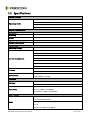
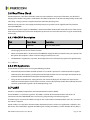
1
G610 GPRS Module Hardware User Manual Version: V1.1.6 Date: 2013-06-04 Confidential Material This document contains information highly confidential to Fibocom Wireless Inc. (Fibocom). Fibocom offers this information as a service to its customers, to support application and engineering efforts that use the products designed by Fibocom. The information provided is based upon requirements specifically provided to Fibocom by the customers. All specifications supplied herein are subject to change. Disclosure of this information to other parties is prohibited without the written consent of Fibocom. Copyright Copy, Reproduce, Distribute and/or Edit of this document or part of it as well as utilization of its contents and communication thereof to others without express authorization are prohibited. Offenders will be held liable for payment of damages. All rights created by patent grant or registration of a utility model or design patent are reserved. Copyright ©2013 Fibocom Wireless Inc. All rights reserved. Trademarks Notice The FIBOCOM Logo is registered by Fibocom Wireless Inc. All other product or service names or logos are the property of their respective owners. Copyright ©2013 Fibocom Wireless Inc. All rights reserved. Revision History Version Date Remarks V1.1.1 2011-11-25 Fix few typing error V1.1.2 2012-03-29 Fix spell mistakes V1.1.3 2012-05-16 Modify table style V1.1.4 2013-01-07 Add reliability features in specifications; update product picture V1.1.5 2013-05-23 Change pin 29 and pin 30 definition V1.1.6 2013-06-04 Update Figure3-3 G610 GPRS Module Hardware User Manual Page 2 of 42 Contents 1 2 3 Introduction .......................................................................................................................................................................................... 5 1.1 Scope ......................................................................................................................................................................................... 5 1.2 Audience .................................................................................................................................................................................. 5 1.3 Applicable Documents ....................................................................................................................................................... 5 1.4 Standards ................................................................................................................................................................................. 5 Overview ................................................................................................................................................................................................ 7 2.1 Description .............................................................................................................................................................................. 7 2.2 Specifications ......................................................................................................................................................................... 8 Hardware Interface Description................................................................................................................................................... 11 3.1 Block Diagram ...................................................................................................................................................................... 11 3.2 Operating Modes ................................................................................................................................................................ 12 3.3 Power Supply ....................................................................................................................................................................... 12 3.4 3.5 3.6 3.7 3.8 3.3.1 Power Supply Design............................................................................................................................................... 13 3.3.2 Power Consumption ................................................................................................................................................ 14 Power On/Off Operation .................................................................................................................................................. 15 3.4.1 Turning on the Module ........................................................................................................................................... 15 3.4.2 Turning off the Module ........................................................................................................................................... 16 Sleep Mode ........................................................................................................................................................................... 17 3.5.1 Activating Sleep Mode ............................................................................................................................................ 18 3.5.2 Serial Interface during Sleep Mode .................................................................................................................... 18 3.5.3 Terminating Sleep Mode ........................................................................................................................................ 19 Real Time Clock.................................................................................................................................................................... 21 3.6.1 VBACKUP Description.............................................................................................................................................. 21 3.6.2 RTC Application ......................................................................................................................................................... 21 UART ........................................................................................................................................................................................ 21 3.7.1 Ring Indicate ............................................................................................................................................................... 22 3.7.2 DCD Indicate ............................................................................................................................................................... 23 SIM Interface ......................................................................................................................................................................... 23 3.8.1 SIM Connection ......................................................................................................................................................... 24 3.8.2 SIM Design Guidelines ............................................................................................................................................ 24 3.8.3 SIM Detected Feature .............................................................................................................................................. 24 G610 GPRS Module Hardware User Manual Page 3 of 42 3.9 3.10 3.11 4 5 Audio Interface .................................................................................................................................................................... 24 3.9.1 The First Audio Channel: Microphone............................................................................................................... 25 3.9.2 The First Audio Channel: Speaker ....................................................................................................................... 25 3.9.3 The Second Audio Channel: Microphone ........................................................................................................ 26 3.9.4 The Second Audio Channel: Speaker................................................................................................................. 26 3.9.5 Audio Design .............................................................................................................................................................. 26 3.9.6 Switch Audio Channel by IO ................................................................................................................................. 27 A/D Interface ........................................................................................................................................................................ 27 3.10.1 Power Supply ADC ............................................................................................................................................... 27 3.10.2 General Purpose ADC ......................................................................................................................................... 28 Controls and Indicators Interface ................................................................................................................................. 28 3.11.1 VDD Reference Regulator ................................................................................................................................. 28 3.11.2 External Reset ........................................................................................................................................................ 29 3.11.3 LPG............................................................................................................................................................................. 29 3.11.4 Trace Ports............................................................................................................................................................... 31 3.11.5 General Purpose I/O ............................................................................................................................................ 31 Electrical and Environmental Features ...................................................................................................................................... 32 4.1 Absolute Maximum Ratings ........................................................................................................................................... 32 4.2 Environmental Specifications ........................................................................................................................................ 32 4.3 Application Interface Specifications ............................................................................................................................ 33 4.4 Pin Definitions...................................................................................................................................................................... 35 Mechanical Design............................................................................................................................................................................ 37 5.1 Mechanical Specifications ............................................................................................................................................... 37 5.2 Recommended PCB Layout ............................................................................................................................................ 38 5.3 Antenna Design................................................................................................................................................................... 39 5.4 Reflow Temperature Profile............................................................................................................................................. 41 Appendix: Glossary..................................................................................................................................................................................... 42 G610 GPRS Module Hardware User Manual Page 4 of 42 1 Introduction 1.1 Scope This manual provides the electrical, mechanical and environmental requirements for properly integrating the G610 GPRS module in a host application. This manual gives a complete set of hardware features and functions that may be provided by G610. The availability of any feature or function, which is described in this manual, depends on the hardware revision and software version of a specific G610 GPRS module. 1.2 Audience This manual is intended for all members of the integration team who are responsible for integrating the G610 module into the host OEM device, including representatives from hardware, software and RF engineering disciplines. 1.3 Applicable Documents G610 GPRS Module brief G610 GPRS Module Hardware User Manual G610 GPRS Module AT Command User Manual G610 GPRS Module AT Command Examples and Steps G610 GPRS Module Developer’s Kit G610 GPRS Module Developer’s Kit User Manual G610 GPRS Module Developer’s Kit Schematics G610 Flash Tool Software (for Windows XP) G610 Mobile Analyzer Software (for Windows XP) G610 Modem Demo Software (for Windows XP) 1.4 Standards ETSI ETS 300 916 (GSM 07.07 version 5.9.1 Release 1996) ETSI TS 100 585 (GSM 07.05 version 7.0.1 Release 1998) ETSI ETS 300 901 (GSM 03.40 version 5.8.1 Release 1996) ETSI TS 100 900 (GSM 03.38 version 7.2.0 Release 1998) ETSI EN 300 607-1 (GSM 11.10-1 version 8.1.1 Release 1999) ETSI TS 100 907 (GSM 02.30 version 6.1.0 Release 1997) ETSI TS 100 549 (GSM 03.90 version 7.0.0 Release 1998) ETSI TS 101 267 (GSM 11.14 version 6.3.0 Release 1997) G610 GPRS Module Hardware User Manual Page 5 of 42 ETSI TS 100 977 (GSM 11.11 version 6.3.0 Release 1997) ITU-T V.25ter ETSI EN 300 908 (GSM 05.02 version 8.5.1 Release 1999) ETSI TS 101 356 (3GPP TS 07.60 version 7.2.0 Release 1998) G610 GPRS Module Hardware User Manual Page 6 of 42 2 Overview This chapter gives a general description of the G610 module. 2.1 Description G610 GPRS Module supports GSM bands 850/900/1800/1900 MHz, with GPRS multi-slot class 10, G610 can operate on any GSM/GPRS network to provide voice and data communications. G610 Q50-00: Quad band (850/900/1800/1900 MHz) G610 A50-00 & G610 A50-01: Dual band (900/1800 MHz) The G610 is similar to a condensed cellular phone core, which can be integrated into any system or product that needs to transfer voice or data information over a cellular network. Thus, it significantly enhances the system's capabilities, transforming it from a standalone, isolated product to a powerful high-performance system with global communications capabilities. The G610 is designed as a complete GSM/GPRS communications solution with all the controls, interfaces and features to support a broad range of applications: A variety set of indicators and control signals More lower power consumption A variety of serial communications solutions. All these features and interfaces are easily controlled and configured using a versatile AT command interface that provides full control over the G610 operation. The G610 control and indication interface extends its capabilities beyond GSM communications. This includes an A/D and GPIO interface, and a regulated output voltage for supplying external circuits. With these interfaces, the G610 can operate and control external applications and receive feedback from external environment and circuits. The G610 is an SMD module, 55 pin. The G610 is extremely compact in size with a slim mechanical design, which makes its space saving on the application board and easily fitted into any board design. The advanced power supply management significantly reduces power consumption to a necessary minimum and prolongs battery life. G610 GPRS Module Hardware User Manual Page 7 of 42 2.2 Specifications Product Features Quad band (Model: G610 Q50-00): Operating Bands 850/900/1800/1900 MHz Dual band (Model: G610 A50-00 & G610 A50-01) 900/1800 MHz Physical Characteristics Dimensions 31.3 mm x 20.2 mm x 3.0 mm Mounting SMT, 55 pin Weight 3.5grams Operational Temperature -40°C to +85°C Storage Temperature -40°C to +85°C Performance Operating Voltage 3.3 – 4.5V (4.0V is recommended) 1.6mA @ Sleep mode 24mA @ Idle mode 260mA @ on call or CSD Current Consumption 420mA @ on GPRS data MAX 2.0A @ Burst 80uA@ Power off 12uA @ RTC only Tx Power Rx Sensitivity 2W, 850/900 MHz 1W, 1800/1900 MHz 850/900MHz: -108dBm 1800/1900MHz: -107dBm Interfaces SIM Card External SIM connectivity 1.8V / 3.0V UART: Serial Ports BR from 1200bps to 230400bps Auto BR from 1200bps to 230400bps Data Features Multi-slot class 10 (4 Rx / 2 Tx / 5 Sum) Max Downlink BR 85.6kbps GPRS Coding scheme CS1-CS4 Class B GSM 07.10 multiplexing protocol G610 GPRS Module Hardware User Manual Page 8 of 42 CSD SMS FAX Max BR 9.6kbps MO/MT Text and PDU modes Cell broadcast Group3 Class 2 (TS 61/62) Voice Features Differential analog audio lines Two channel Vocoders EFR/HR/FR/AMR DTMF Support Audio Control Echo suppression, noise suppression, side tone and gain control Reliability Features Item Low-temperature Storage High-temperature Storage Low-temperature Working High-temperature Working Test Condition Temperature: –40±2ºC Test Duration: 24 h Temperature: 85±2ºC Test Duration: 24 h Temperature: –40±2ºC Test Duration: 24 h Temperature: 85±2ºC Test Duration: 24 h Standard IEC60068 IEC60068 IEC60068 IEC60068 High Temperature: 55±2ºC Low Temperature: 25±2ºC Damp Heat Cycling Humidity: 95% IEC60068 Repetition Times: 4 Test Duration: 12 h + 12 h Low Temperature: –40±2ºC High Temperature: 85±2ºC Temperature Shock Temperature Change Interval: < 30s IEC60068 Test Duration: 15 min Repetition Times: 100 Frequency Range: 5 Hz to 200 Hz Acceleration: 10 m/s2 Sine Vibration Frequency Scan Rate: 1 oct/min IEC60068 Test Period: 3 axial directions. Five circles for each axial direction. Half-sine Wave Shock Shock Test Peak Acceleration: 300 m/s2 IEC60068 Shock Duration: 11 ms G610 GPRS Module Hardware User Manual Page 9 of 42 Test Period: 6 axial directions. One shock for each axial direction. Half-sine Wave Peak Acceleration: 180 m/s2 Clash Test Pulse Duration: 6 ms IEC60068 Repetition Time: 6 directions. 1000 times for each direction. Others ADC Detect BATT voltage Detect extend analog voltage RTC Inside Flexible Status Indicator Extend Reset G610 GPRS Module Hardware User Manual Page 10 of 42 3 Hardware Interface Description The following paragraphs describe in details the hardware requirements for properly interfacing and operating the G610 module. 3.1 Block Diagram The G610 consists of the following blocks: Figure 3-1 Digital Block Micro-controller Unit (MCU) for system and application code execution Digital Signal Processor (DSP) for voice and data processing Serial communications interfaces SPI for trace debug or PCM audio (option) SIM card General purpose IO signals Real Time Clock (RTC) subsystem Analog Block Power management inside Internal regulators Analog audio interface management General purpose dedicated A/D signals BATT voltage A/D inside G610 GPRS Module Hardware User Manual Page 11 of 42 GSM Transceiver Block 3 gain stages for the low GSM band and high GSM band 850/900/1800/1900 MHz RF receiver, which includes LNAs, Mixers, VCOs, I/Q outputs and buffers Signal processing IC for transmit and receive GSM data processing FEM - Front End Module Includes a harmonic filter and antenna switch Filter - Quad-band SAW filter that selects the required receive band 3.2 Operating Modes The module incorporates several operating modes. Each operating mode is different in the active features and interfaces. The table summarizes the general characteristics of the module operating modes and provides general guidelines for operation. Operating Modes Description Features Not Powered BATT & Vbackup supply is disconnected. The G610 is off. Any signals connected to the interface connector must be set low or tri-state. Power off Mode Valid BATT supply but not power on. After reset module. Vbackup output and VDD is off. The G610 MCU/DSP/RF is Off. The PMU is operating in RTC mode. Any signals connected to the interface connector must be set low or tri-state. RTC Mode Power off mode BATT supply is disconnected. But valid Vbackup supply The G610 MCU/DSP/RF is Off. The PMU is operating in RTC mode. Any signals connected to the interface connector must be set low or tri-state. Idle Mode Power on is succeeded and VDD output. CTS_N and DSR_N signals are enabled (low). The G610 is fully active, registered to the GSM/GPRS network and ready to communicate. Note: This is the default power-on mode. CTS_N signal is wave. The G610 is in low power mode. The application interfaces are disabled, but, G610 continues to monitor the GSM network. LPG signal is toggling. A GSM voice or data call is in progress. When the call terminates, G610 returns to the last operating state (Idle or Sleep). Sleep Mode Call or CSD call or GPRS data 3.3 Power Supply The G610 power supply must be a single external DC voltage source of 3.3V to 4.5V. The power supply must be able to sustain the voltage level during a GSM transmit burst current serge, which may reach 2.0A. G610 GPRS Module Hardware User Manual Page 12 of 42 The G610 interface connector has 2 pins for the main power supply, as described in the table. All these contacts must be used for proper operation. Pin# Signal Name Description 26 27 BATT DC power supply. BATT = 3.3V to 4.5V, 4.0V is recommended GND Ground 1 21 22 24 25 28 46 3.3.1 Power Supply Design Special care must be taken when designing the power supply of the module. The single external DC power source indirectly supplies all the digital and analog interfaces, but also directly supplies the RF power amplifier (PA). Therefore, any degradation in the power supply performance, due to losses, noises or transients, will directly affect the module performance. The burst-mode operation of the GSM transmission and reception draws instantaneous current surges from the power supply, which causes temporary voltage drops of the power supply level. The transmission bursts consume the most instantaneous current, and therefore cause the largest voltage drop. If the voltage drops are not minimized, the frequent voltage fluctuations may degrade the module performance. Figure 3-2 It is recommended that the voltage drops during a transmit burst will not exceed 300mV, measured on the module interface connector. In any case, the module supply input must not drop below the minimum operating level during a transmit burst. Dropping below the minimum operating level may result in a low voltage detection, which will initiate an automatic power-off. To minimize the losses and transients on the power supply lines, it is recommended to follow these guidelines: G610 GPRS Module Hardware User Manual Page 13 of 42 Use a 1000uF or greater, low ESR capacitor on the module supply inputs. The capacitor should be located as near to the module interface connector as possible. Use low impedance power source, cabling and board routing. Use cabling and routing as short as possible. Filter the module supply lines using filtering capacitors, as described in the table. Recommended Capacitor Usage Description 1000uF GSM Transmit current serge Minimizes power supply losses during transmit bursts. Use maximum possible value. 10nF, 100nF Digital switching noise 8.2pF, 10pF 33pF, 39pF 1800/1900 MHz GSM bands 850/900 MHz GSM bands Filters digital logic noises from clocks and data sources. Filters transmission EMI. Filters transmission EMI. 3.3.2 Power Consumption The table specifies typical module current consumption ratings in various operating modes. The current ratings refer to the overall module current consumption over the BATT supply. Measurements were taken under the following conditions: BATT = 4.0V Operating temperature 25°C Registered to a GSM/GPRS network The actual current ratings may vary from the listed values due to changes in the module's operating and environment conditions. This includes temperature, power supply level and application interface settings. Parameter Description I off Power off mode I idle I sleep I gsm-avg Conditions Min Typical Max Unit 80 90 µA Idle mode GSM only, DRX=2, -85dBm GSM850/900 DSC/PCS 24 mA Low power mode DRX=2 5 9 3.6 2.0 1.6 mA Average current GSM voice 1 TX slot 1 Rx slot GSM850/900 PCL=5 10 15 19 DCS/PCS PCL=0 5 10 15 260 150 115 110 230 140 115 110 mA G610 GPRS Module Hardware User Manual Page 14 of 42 I gsm-max I gprs-avg Average current GSM voice 1 TX slot 1 Rx slot Average current GPRS Class 10 2 TX slot 2 Rx slot 1800 GSM850/900 PCL=5 19 DCS/PCS PCL=0 15 300 1400 300 GSM850/900 PCL=5 19 DCS/PCS PCL=0 15 420 150 380 150 2000 mA mA 3.4 Power On/Off Operation The module power on and off is the two primary phases, which are related at the interface connector by the hardware signals POWER_ON, VDD. The POWER_ON signal is main controller. The VDD signal indicates whether module is powered on or off. When this signal is disabled (0V), module is powered-off. When it is output (2.85V), module is powered-on. Note: When the VBAT power supplied, the module will be turn on automatically. It’s the default power on mode. The VDD would be flowed backwards by other IOs which be connected extend voltage. So DSR/CTS/LPG can be indicated the powered on process replaced. Because of the BOOT feature, the TXD_N should be pulled up continuously between the module turn on process. Pin# Signal Name Description 10 POWER_ON Power on and off module, low level activated VDD Illustrating module start up LDO power output 0V : G610 is power off LDO power output 2.85V : G610 is start up 9 3.4.1 Turning on the Module When the module is powered off, the PMU operates at low power mode, with only the RTC timer active. The module will power on again when the POWER_ON signal is falling edge. Asserting the POWER_ON signal low for a minimum of 800 milliseconds will turn the module on in default power on mode. Note: The G610 A50-01 module will not be turned on automatically. The POWER_ON signal should be low for 1600-1800 milliseconds to turn G610 A50-01 on. G610 GPRS Module Hardware User Manual Page 15 of 42 The following figure illustrates power on succeeded. Figure 3-3 The following figure illustrates power on is failed. Figure 3-4 3.4.2 Turning off the Module There are several ways to turn off the module: Asserting the POWER_ON signal low for a minimum of 3 seconds. Under voltage automatic shutdown or the module can be powered off using AT command, please refer to G600&G610 GPRS Module AT Command User Manual. 1. POWER_ON Signal The POWER_ON signal is set high using an internal pull up resistor when power is applied to the module. When the POWER_ON signal is falling edge and keeping low for a minimum of 3 seconds will turn the module off. This will initiate a normal power-off process, which includes disabling of all applications interfaces (UART, SIM card, audio, etc.) and logout the network connection. G610 GPRS Module Hardware User Manual Page 16 of 42 Figure 3-5 2. Under Voltage automatic shutdown A low power shut down occurs when G610 senses the external power supply is below the minimal operating limit (VBAT≤3.2V). The module will respond by powering down automatically without notice. This form of power-down is not recommended for regular use since the unexpected power loss may result in loss of data. 3. AT Command +MRST The AT+MRST command initiates a G610 power off operation, which powers off directly. +CFUN The AT+CFUN=0 command initiates a G610 power off operation, which de-registration first, and then powers off. 3.5 Sleep Mode The module incorporates an optional low power mode, called Sleep Mode, in which it operates in minimum functionality, and therefore draws significantly less current. During Sleep Mode the module network connection is not lost. The module will be waked up cycled and monitored the GSM network constantly for any incoming calls or data. During Sleep mode, all of the G610 interface signals are inactive and are kept in their previous state, prior to activating low power mode. To save power, all the module internal clocks and circuits are shut down, and therefore serial communications is limited. The CTS_N signal is alternately enabled (LOW level) and disabled (HIGH level) synchronously with Sleep Mode and Idle mode. At the same time this indicates the module serial interfaces are active. G610 will not enter Sleep mode in any case when there is data present on the serial interface or incoming from the GSM network or an internal system task is running. Only when processing of any external or internal system task has completed, G610 will enter Sleep mode according to the ATS24 command settings. G610 GPRS Module Hardware User Manual Page 17 of 42 All of the description about CTS_N, it must be set the UART to HARDWARE FLOW control by AT command. 3.5.1 Activating Sleep Mode By default, the G610 powers on in Idle Mode. The ATS24 default is 0. In this mode the G610 interfaces and features are functional and the module is fully active. Sleep mode is activated by the ATS24 command. Such as ATS24 would be activated Sleep mode at soon. Figure 3-6 3.5.2 Serial Interface during Sleep Mode The module wakes up periodically from Sleep mode to page the GSM network for any incoming calls or data. After this short paging is completed, module returns to Sleep mode. During this short awake period, the serial interfaces are enabled and communications with the module is possible. The CTS_N signal is alternately enabled and disabled synchronously with the network paging cycle. CTS_N is enabled whenever module awakes to page the network. The period based on the DRX parameter of the network. 4.615ms (TDMA frame duration) * 51 (number of frames) * DRX value At the same time, the CTS_N indicates the G610 serial interfaces are active or inactive. Figure 3-7 G610 GPRS Module Hardware User Manual Page 18 of 42 3.5.3 Terminating Sleep Mode Terminating the Sleep mode, or wake-up, is defined as the transition of the G610 operating state from Sleep mode to Idle mode. There are several ways to wake-up G610 from Sleep mode as described below. During Sleep mode the G610 internal clocks and circuits are disabled, in order to minimize power consumption. When terminating the Sleep mode, and switching to Idle mode, G610 requires a minimal delay time to reactivate and stabilize its internal circuits before it can respond to application data. This delay is typically of 5ms, and is also indicated by the CTS_N signal inactive (high) state. The delay guarantees that data on the serial interface is not lost or misinterpreted. 3.5.3.1 Temporary Termination of Low Power Mode Temporary termination of Sleep mode occurs when G610 switches from Sleep mode to Idle mode for a defined period, and then returns automatically to Sleep mode. Low power mode may be terminated temporarily by several sources, some of which are user initiated and others are initiated by the system. Incoming Network Data During Sleep mode, G610 continues monitoring the GSM network for any incoming data, message or voice calls. When G610 receives an indication from the network that an incoming voice call, message or data is available, it automatically wakes up from Sleep mode to alert the application. When G610 wakes up to Idle mode all its interfaces are enabled. Depending on the type of network indication and the application settings, G610 may operate in several methods, which are configurable by AT commands, to alert the application of the incoming data: 1) Enable the serial interface's CTS_N 2) Send data to the application over the serial interface. 3) Enable the serial interface's Ring Indicator (RING_N) signal. 4) LPG status indicator Data on the Serial interface During Sleep mode, serial communications is limited to short periods, while G610 is paging the network. When the serial interface is active, data can be exchanged between the application and the G610. The G610 will not return to Sleep mode until the serial interface transmission is completed and all the data is processed. Only when the serial interface transfer is completed and the data is processed, G610 will return to Sleep mode automatically, according to the ATS24 settings. G610 GPRS Module Hardware User Manual Page 19 of 42 ATS24=1 CTS RXD Figure 3-8 1) The G610 serial interface is set HARDWARE FLOW (AT+IFC=2,2) When the following conditions are true, the G610 will receive the data from a DTE (Data Terminal Equipment) and go back to Idle mode for response. a) G610 serial interface is set HARDWARE FLOW by AT+IFC command. b) The RTS/CTS of G610 were connected to the DTE (Data Terminal Equipment). c) The DTE serial interface is running with HARDWARE FLOW. 2) The G610 serial interface is set NONE FLOW (AT+IFC=0,0)(The default value) Most of serial data from DTE to G610 will be lost when the G610 serial interface is set NONE FLOW (default value). The G610 will receive the data and make responses after it go back to Idle mode. DTR signal trigger During Sleep mode, DTR signal can be triggered the module back to Idle mode. GPRS DTR Module T >= 50mS It recommends that the serial data should better be sent to module 20mS later when DTR triggered. If there isn’t any other termination status the module will go back to Sleep mode depend on ATS24 value. 3.5.3.2 Permanent termination of Sleep Mode The module Sleep mode is enabled and disabled by the ATS24 command. ATS24 : ATS24 = 0 disables Sleep mode. The value of ATS24 (>0) will be saved but the mode will not be save by re-power G610. G610 GPRS Module Hardware User Manual Page 20 of 42 3.6 Real Time Clock G610 incorporates a Real Time Clock (RTC) mechanism that performs many internal functions, one of which is keeping time. The RTC subsystem is embedded in the PMU and operates in all of the G610 operating modes (Off, Idle, Sleep), as long as power is supplied above the minimum operating level. When the main power was not supply, the backup battery or capacitor can be supplied to RTC by interface connector VBACKUP. When the main power supply and VBACKUP is disconnected from G610, the RTC timer will reset and the current time and date will be lost. On the next G610 power-up the time and date will need to be set again automatically or manually. 3.6.1 VBACKUP Description Pin# Signal Name Description 8 VBACKUP Real time clock power When main power BATT is supplied. The VBACKUP output 2.0V for external battery or capacitor charging. The charging current base on external resistor. When main power BATT is disconnected. The VBACKUP supply the RTC by External battery or capacitor. The RTC power consumption is about 12uA. The voltage cannot be over 2.2V. The VBACKUP is supplied by a capacitor. The backup time can be calculated by capacitance approximately. T(s) ≈ C(uF)/1.3 3.6.2 RTC Application The G610 time and date can be set using the following methods: Automatically retrieved from the GSM network. In case G610 is operated in a GSM network that supports automatic time zone updating, it will update the RTC with the local time and date upon connection to the network. The RTC will continue to keep the time from that point. Using the AT+CCLK command. Setting the time and date manually by this AT commands overrides the automatic network update. Once the time and date are manually updated, the RTC timer will keep the time and date synchronized regardless of the G610 operating state. 3.7 UART G610 has a completely independent serial communications interface (UART). The G610 UART is a standard 8-signal bus. This UART is used for all the communications with G610 - AT commands interface, GPRS/EGPRS data and CSD data, programming and software upgrades. The UART signals are active low CMOS level signals. For standard RS232 communications with a PC, an external transceiver is required. G610 is defined as a DCE (Data Communications Equipment) device, and the user application is defined as the DTE device. These definitions apply for the UART signals naming conventions, and the direction of data flow, as G610 GPRS Module Hardware User Manual Page 21 of 42 described in the figure. Pin# Signal Name Description Feature Direction 45 RXD_N Module Transmitted Data DTE Received Data DCE→DTE 44 TXD_N Module Received Data DTE Transmitted Data DTE→DCE 39 RING_N Module Ring indicator Notice DTE Remote Call DCE→DTE 38 DSR_N Module Data Set Ready DCE Was Ready DCE→DTE 42 RTS_N Request To Send DTE Notice DCE Requested To Send DTE→DCE 40 DTR_N Data Terminal Ready DTE Was Ready DTE→DCE 43 CTS_N Module Clear To Send DCE Switch To Received Mode DCE→DTE 41 DCD_N Data Carrier Detect Data Carrier Was Online DCE→DTE Recommended connection: Application MCU Direction Module RXD Pin 45 RXD_N TXD Pin 44 TXD_N RI Pin 39 RING_N DSR Pin 38 DSR_N RTS Pin 42 RTS_N DTR Pin 40 DTR_N CTS Pin 43 CTS_N DCD Pin 41 DCD_N The G610 UART supports baud rates 1200, 2400, 4800, 9600, 19200, 38400, 57600, 115200, 230400bps. Auto baud rate detection is supported for baud rates up to 230400bps. All flow control handshakes are supported: hardware or none. The UART default port configuration is 8 data bits, 1 stop bit and no parity, with NONE FLOW control and auto baud rate detect enabled. Note: The auto baud will be availability at the first time after power on. The UART will be no answer probably if switch to another baud rate at working. 3.7.1 Ring Indicate The RING_N signal serves to indicate incoming calls and other types of URCs (Unsolicited Result Code). It can also be used to send pulses to the host application, for example to wake up the application from power saving state. In IDLE mode, the RING_N is high. It is only indicating a type of event at a time: G610 GPRS Module Hardware User Manual Page 22 of 42 1) When a voice call comes in, the RING_N line goes low for 1 second and high for another 4 seconds. Every 5 seconds as a cycle. Figure 3-9 2) When a FAX call comes in, the RING_N line low for 1s and high for another 4s. Every 5 seconds as a cycle. 3) When a Short massage comes in, the RING_N line to low for 150mS, and always high. 3.7.2 DCD Indicate The DCD_N signal serves to indicate CSD call or GPRS data mode. The detail definition refers to AT&C command. 3.8 SIM Interface The G610 incorporates a SIM interface, which conforms to the GSM 11.11 and GSM 11.12 standards, which are based on the ISO/IEC 7816 standard. These standards define the electrical, signaling and protocol specifications of a GSM SIM card. The module does not incorporate an on-board SIM card tray for SIM placement. The SIM must be located on the user application board, external to the G610. The G610 SIM interface includes all the necessary signals, which are routed to the interface connector, for a direct and complete connection to an external SIM. The module supports 1.8V or 3.0V SIM card automatic. While the module turn on by POWER_ON. At first SIM_VCC output 1.8V voltage for external SIM card communication. If it is not successful SIM_VCC output 2.85V voltage and communicated SIM card again. Note: If SIM_VCC is supplied, remove SIM card is prohibited. In case, it would damage both SIM card and G610. Pin# Signal Name Description 5 SIM_CLK Serial 3.25MHz clock 2 SIM_VCC 1.8V or 2.85V Supply to the SIM 4 SIM_DATA Serial input and output data 6 SIM_RST Active low SIM reset signal 3 SIM_CD SIM card on site detected G610 GPRS Module Hardware User Manual Page 23 of 42 3.8.1 SIM Connection The figure illustrates a typical SIM interface connection to G610. This connection type is implemented on the G610 Developer Board, using an MOLEX SIM tray, PN 912283001 & 912360001. Figure 3-10 3.8.2 SIM Design Guidelines The SIM interface and signals design is extremely important for proper operation of the module and the SIM card. There are several design guidelines that must be followed to achieve a robust and stable design that meets the required standards and regulations. The SIM should be located, and its signals should be routed, away from any possible EMI sources, such as the RF antenna and digital switching signals. The SIM interface signals length should not exceed 100mm between the module interface connector and the SIM tray. This is to meet with EMC regulations and improve signal integrity. To avoid crosstalk between the SIM clock and data signals (SIM_CLK and SIM_DATA), it is recommended to rout them separately on the application board, and preferably isolated by a surrounding ground plane. The SIM card signals should be protected from ESD using very low capacitance protective elements (zener diodes, etc.). The recommended part no of ESD is AVR-M1005C080MTAAB (TDK). We also recommended the ESD component should layout with SIM hold closely. 3.8.3 SIM Detected Feature When set AT+MSMPD=1, the SIM detected feature will be actives. The SIM card is on site or not will be detected with SIM_CD pin. SIM_CD=Low level, SIM card is onsite and register the network automatically. SIM_CD=High or NC, SIM card is off site and G610 drop out the network. Note: The default value of MSMPD parameter is “0”. And also, the SIM detected feature was disabled correspondingly. 3.9 Audio Interface The module audio interface supports two channel audio devices and operating modes. The audio interface's G610 GPRS Module Hardware User Manual Page 24 of 42 operating modes, active devices, amplification levels and speech processing algorithms are fully controlled by the host application, through advanced programming options and a versatile AT commands set. Pin# Signal Name Description 13 MIC- 14 MIC+ 1st Audio channel Balanced microphone input 11 AUXI+ 12 AUXI- 16 EAR- 15 EAR+ 18 AUXO+ 17 AUXO- 2nd Audio channel Balanced microphone input 1st Audio channel Output is balanced and can directly operate an head set 2nd Audio channel Output is balanced and can directly operate an hand free speaker 3.9.1 The First Audio Channel: Microphone This channel is the module power-up default active audio channel. The microphone input includes all the necessary circuitry to support a direct connection to an external microphone device. It incorporates an internal bias voltage which can be adjusted by AT command. It has an impedance of 2kΩ. The bias voltage would be supplied after a voice call establish. Parameter Conditions Min Typical Max Unit Bias Voltage No load 1.8 2.0 2.2 V Gain Programmable in 3dB steps 0 45 dB 2 AC Input Impedance kΩ 3.9.2 The First Audio Channel: Speaker This channel is the module power-up default active output for voice calls and DTMF tones. It is designed as a differential output with 32Ω impedance. Parameter Conditions Output Voltage No load Single ended Min Typical Max Unit 200 mVPP AC Output Impedance 32 Ω DC Voltage 1.38 V G610 GPRS Module Hardware User Manual Page 25 of 42 3.9.3 The Second Audio Channel: Microphone This channel is switched on by AT Command. The microphone input includes all the necessary circuitry to support a direct connection to an external microphone device. It incorporates an internal bias voltage which can be adjusted by AT command. It has an impedance of 2kΩ. The bias voltage would be supplied after G610 powered on. Parameter Conditions Bias Voltage No load Gain Programmable in 3dB steps Min Typical 0 Max Unit 2.5 V 45 dB 2 AC Input Impedance kΩ 3.9.4 The Second Audio Channel: Speaker This channel is switched on by AT Command. It is designed as a differential output and can be droved an 8Ω speaker directly. Parameter Conditions Output Voltage No load Single ended Min Typical Max Unit 500 mVPP AC Output Impedance 8 Ω DC Voltage 1.38 V 3.9.5 Audio Design The audio quality delivered by module is highly affected by the application audio design, particularly when using the analog audio interface. Therefore, special care must be taken when designing the module audio interface. Improper design and implementation of the audio interface will result in poor audio quality. Poor audio quality is a result of electrical interferences, or noises, from circuits surrounding the audio interface. There are several possible sources for the audio noise: Transients and losses on the power supply EMI from antenna radiations Digital logic switching noise Most of the audio noise originates from the GSM transmit burst current surges (217Hz TDMA buzz), which appear on the main power supply lines and antenna, but also indirectly penetrate the internal application's supplies and signals. The noises are transferred into the G610's audio circuits through the microphone input signals and then are amplified by the G610's internal audio amplifiers. To minimize the audio noise and improve the audio performance the microphone and speaker signals must be G610 GPRS Module Hardware User Manual Page 26 of 42 designed with sufficient protection from surrounding noises. The following guidelines should be followed to achieve best audio performance: Reference the microphone input circuits to the G610 AGND interface signal. If using single-ended audio outputs, they should be referenced to the G610 AGND interface signal. Keep the audio circuits away from the antenna. Use RF filtering capacitors on the audio signals. The audio signals should not be routed adjacent to digital signals. Isolate the audio signals by a surrounding ground plane or shields. Filter internal supplies and signals that may indirectly affect the audio circuits, from noises and voltage drops. 3.9.6 Switch Audio Channel by IO The module support switch audio channel by IO pin. The default level of this pin is high. This IO pin is took effect under 1st channel is activated. When the IO is pulled low, the audio channel will be switched from 1st channel to 2nd channel automatically. When the IO level is back to High, the audio channel will be back to 1st channel. If the audio 2nd channel is activated, this PIN will not do any effect at all. Pin# 47 Signal Name Description HS_DET 1st channel is activated. Level = Low, the 2nd channel is activated Level = High, back to the 1st channel Note:After the MAPATH command was switch the audio channel, this PIN does not effect at all. 3.10 A/D Interface The G610 includes 3 Analog to Digital Converter (ADC) (2 ADC and 1 BATT ADC) signals with 12-bit resolution, for environmental and electrical measurements. The ADC signals accept an analog DC voltage level on their inputs and convert it to a 12-bit digital value for further processing by G610 or the user application. In Idle mode, the ADC input is sampled consecutive times by sampling time interval, and the lasted 8 samples are compared and averaged to provide a stable and valid result. In Sleep mode, the ADC is stopped. When the G610 switch to Idle mode, the ADC should be stable after 5mS. 3.10.1 Power Supply ADC The main power supply (BATT) is sampled internally by the G610 ADC interface through a dedicated input, which is not accessible on the interface connector. The G610 constantly monitors the power supply for any low or high voltage. G610 GPRS Module Hardware User Manual Page 27 of 42 Parameter Conditions Min Supply Range Operating range 3.20 Resolution Typical Max Unit 4.50 V 1.0 Sampling Time % 16 KHz The ADC signals operation and reporting mechanism is defined by the AT+CBC command. 3.10.2 General Purpose ADC The G610 provides 2 general purpose ADC signal for customer application use. The ADC signal can monitor a separate external voltage and report its measured level independently to the application, through the AT command interface. Pin# Signal Name Description 19 ADC2 General purpose ADC 20 ADC1 General purpose ADC Parameter Conditions Min Input Voltage Operating range 0 Resolution Typical Max Unit 1.00 V 0.5 Sampling Time % 16 KHz The ADC signals operation and reporting mechanism is defined by the AT+MMAD command. 3.11 Controls and Indicators Interface The module incorporates several interface signals for controlling and monitoring the module's operation. The following paragraph describes these signals and their operation. Pin# Signal Name 9 VDD 49 LPG 7 RESET_N Description LDO power output Illustrating module start up Module work status indicator Extend reset module Low level activated 3.11.1 VDD Reference Regulator The G610 incorporates a regulated voltage output VDD. The regulator provides a 2.85V output for use by the customer application. This regulator can source up to 10mA of current to power any external digital circuits. When the G610 started up by power on signal, The VDD is output. So it can be Illustrating module start up. G610 GPRS Module Hardware User Manual Page 28 of 42 Note: The VDD regulator is powered from the G610's main power supply, and therefore any current sourced through this regulator originates from the G610 BATT supply. The overall BATT current consumed by G610 is directly affected by the VDD operation. The G610 current consumption raises with respect to the current sourced through VDD. Parameter Conditions Min Typical Max Unit Vout Iout=30mA -3% 2.85 3% V 10 30 mA 150 mA 35% uF Iout Imax Current pulled down from LDO to GND until LDO voltage is 50% of nominal value External Capacitor PSRR -35% 50Hz - 20kHz 1 35 dB 3.11.2 External Reset The RESET_N input signal would be power off the G610 immediately. This signal is set high after power up, when G610 is operating. It is set low when G610 is powered off. When the RESET_N signal is low, the G610 is powered off without the work net logging out. Note: It’s recommended that it should connect the 1nF capacitor to GND on external circuit. Parameter Conditions T width Min Typical Max Unit 100 200 400 mS 3.11.3 LPG As an alternative to generating the synchronization signal, the control pin can be used to drive a status LED on application platform. The timing of LPG, it can be indicated the G610 status straight. Referenced circuits about LED driver see below. Figure 3-11 States of the LED vs PIN: LED Off = HIGH. LED On = LOW. G610 GPRS Module Hardware User Manual Page 29 of 42 LED State Operating Status of G610 G610 is in one of the following modes: • Power off mode • SLEEP mode G610 is in one of the following status: • NO SIM card 600ms on / 600ms off • SIM PIN • Register network (T<15S) • Register network failure (always) G610 is in one of the following status: 3s on / 75ms off • IDLE mode G610 is in one of the following status: 75ms on / 75ms off • One or more GPRS contexts activated. G610 is in one of the following status: Permanently on • Voice call • CSD or FAX call When the G610 POWER ON, the LPG timing see as below: Permanently off POWER_ON Register network IDLE mode Figure 3-12 G610 GPRS Module Hardware User Manual Page 30 of 42 3.11.4 Trace Ports The GSM/GPRS network and the module is incorporated a complicated system. The module prepared the trace function for debugged or acquired the data of the system. The module transfers these data from SPI port. It can be operated on the PC software and execute by SPI adaptor to RS232. Note: It’s recommend that reserved these ports and connected to a socket in any design. Pin# Signal Name Description 53 PCM_DIN TR_MISO Trace data input 50 PCM_FS TR_MOSI Trace data output 52 PCM_CLK TR_CLK Trace clock output 51 PCM_DOUT TR_CS General purpose I/O 48 TR_INT Trace Interrupt Input 3.11.5 General Purpose I/O The G610 incorporates 8 general purpose IO signals for the user application. Each GPIO signal may be configured and controlled by AT command. These signals may be used to control or set external application circuits, or to receive indications from the external application. Pin# Signal Name Description 35 GPIO01 Bit1 34 GPIO02 Bit2 33 GPIO03 Bit3 32 GPIO04 Bit4 37 SCL/GPIO18 Bit5 36 SDA/GPIO19 Bit6 31 GPIO07 Bit7 54 GPIO36 Bit8 G610 GPRS Module Hardware User Manual Page 31 of 42 4 Electrical and Environmental Features 4.1 Absolute Maximum Ratings The table gives the maximum electrical characteristics of the module interface signals. Note: Using the G610 module beyond these conditions may result in permanent damage to the module. Parameter Conditions BATT Supply G610 powered on Digital Input Signals VDD Domain Analog Input Signals (Audio, A/D interfaces) G610 powered on Min Max Unit -0.2 4.5 V -0.2 3.3 V -0.2 2.75 V 4.2 Environmental Specifications The table gives the environmental operating conditions of the module. Note: Using the G610 module beyond these conditions may result in permanent damage to the module. Parameter Min Max Unit Operating Temperature -40 +85 °C Storage Temperature -40 +85 °C ±4 KV ±8 KV ESD Conditions (Contact) Antenna connector (Air) Antenna connector G610 GPRS Module Hardware User Manual Page 32 of 42 4.3 Application Interface Specifications The table summarizes the DC electrical specifications of the application interface connector signals. Note: Interface signals that are not used by the customer application must be left unconnected. G610 incorporates the necessary internal circuitry to keep unconnected signal in their default state. Do not connect any components to, or apply any voltage on, signals that are not used by the application. G610 Pin# G610 Signal Name Description I/O BATT DC power supply I GND Ground 8 VBACKUP Real time clock power 29 NC No connect _ 30 NC No connect _ Reset level Idle level Level Character Power 26 27 3.3V ~ 4.5V 1 21 22 24 25 28 46 I/O 2.0V 2.0V 1.86V ~ 2.14V, Output current <3mA, Input current <12uA Control & Status 49 LPG Work mode indicator O CP Wave VOL MAX =0.35V VOH MIN =VDD-0.35V 9 VDD LDO power output Illustrating start up O 0.3V 2.85V ±3% Output current <10mA 7 RESET_N Extend reset** Low level activated I PU/HZ H VIL MAX =0.2V VIH MIN =0.7*VDD 10 POWER_ON Turn on module Low level activated I PU/HZ H VIL MAX =0.2V VIH MIN =0.7*VDD 220K PU to VBACKUP O CP H I CP H Uart (Modem DCE) DTE: Received Data 45 RXD_N 44 TXD_N 39 RING_N Ring indicator O CP H 38 DSR_N Data Set Ready O CP H 42 RTS_N Request To Send I CP H 40 DTR_N Data Terminal Ready I CP H 43 CTS_N Clear To Send O CP L DCE: Transmitted Data DTE: Transmitted Data DCE: Received Data G610 GPRS Module Hardware User Manual VOL MAX =0.35V VOH MIN =VDD-0.35V VIL MAX =0.2V VIH MIN =0.7*VDD Page 33 of 42 41 DCD_N Data Carrier Detect O CP H SIM Interface (3.0V) 2 SIM_VCC SIM power O 0.3V 1.8V 2.85V 5 SIM_CLK SIM clock O T 3.25MHz 4 SIM_DATA SIM data I/O OD/PD Wave 6 SIM_RST SIM reset O T L 3 SIM_CD SIM on site detect High level is on site I T L ±3% Output current <10mA VOL MAX =0.35V VOH MIN =VSIM-0.35V VIL MAX =0.2V VIH MIN =0.7*VSIM PCM audio / Trace (SPI) 53 PCM_DIN Trace data input I CP H 50 PCM_FS Trace data output O CP H 52 PCM_CLK Trace clock output O CP L 51 PCM_DOUT General purpose I/O O CP H 48 TR_INT Trace Interrupt Input I CP H 13 MIC- 14 MIC+ 1st Audio channel (default) Balanced input I 0V 0V 11 AUXI+ 12 AUXI- 2nd Audio channel Balanced input I 0V 16 EAR- 15 EAR+ 1st Audio channel (default) Balanced output O 0V 0V 18 AUXO+ 17 AUXO- 2nd Audio channel Balanced output O 0V 1.0V 23 RF_ANT RF antenna port 47 HS_DET Headset detect 19 ADC2 General purpose A/D I 0V 0V 0V ~ 1.000V 20 ADC1 General purpose A/D I 0V 0V 0V ~ 1.000V 36 SDA/GPIO19 I2C_SDA I/O OD OD 37 SCL/GPIO18 I2C_SCL I/O OD OD 31 GPIO07 General purpose IO I T T 35 GPIO01 General purpose IO O T T 34 GPIO02 General purpose IO O T T 33 GPIO03 General purpose IO O T T 32 GPIO04 General purpose IO O T T 54 GPIO36 General purpose IO O CP H 55 NC VOL MAX =0.35V VOH MIN =VDD-0.35V VIL MAX =0.2V VIH MIN =0.7*VDD Audio 2.85V 0V Discrete G610 GPRS Module Hardware User Manual Extend voltage VOL MAX =0.35V VOH MIN =VDD-0.35V VIL MAX =0.2V VIH MIN =0.7*VDD Page 34 of 42 Note: CP=Center Pin; T= 3 Status; PD= Pull Down; PU=Pull Up; OD=Open Drain The sum of sank or sourced currents in the connection between the IO cannot exceed 10mA @ 3.3V. 4.4 Pin Definitions Pin 55 Pin 28 Pin 1 Pin 27 Figure 4-1 Pin No. Signal Name Pin No. Signal Name 1 GND 55 NC 2 SIM_VCC 54 GPIO36 3 SIM_CD 53 PCM_DIN 4 SIM_DATA 52 PCM_CLK 5 SIM_CLK 51 PCM_DOUT 6 SIM_RST 50 PCM_FS 7 RESET_N 49 LPG 8 VBACKUP 48 TR_INT 9 VDD 47 HS_DET 10 POWER_ON 46 GND 11 AUXI+ 45 RXD_N 12 AUXI- 44 TXD_N 13 MIC- 43 CTS_N 14 MIC+ 42 RTS_N G610 GPRS Module Hardware User Manual Page 35 of 42 Pin No. Signal Name Pin No. Signal Name 15 EAR+ 41 DCD_N 16 EAR- 40 DTR_N 17 AUXO- 39 RING_N 18 AUXO+ 38 DSR_N 19 ADC2 37 SCL/GPIO18 20 ADC1 36 SDA/GPIO19 21 GND 35 GPIO01 22 GND 34 GPIO02 23 RF_ANT 33 GPIO03 32 GPIO04 24 GND 31 GPIO07 25 GND 30 NC 26 BATT 29 NC 27 BATT 28 GND G610 GPRS Module Hardware User Manual Page 36 of 42 5 Mechanical Design 5.1 Mechanical Specifications The following figure shows the mechanical specifications of the module in details: Figure 5-1 G610 GPRS Module Hardware User Manual Page 37 of 42 5.2 Recommended PCB Layout The following figure shows recommended PCB Layout. Figure 5-2 G610 GPRS Module Hardware User Manual Page 38 of 42 5.3 Antenna Design The RF I/O Antenna signal is by default provided to 50ohm antenna interface. In user’s main board, the Antenna layout should be design 50ohm Microstrip Transmission Line. The Microstrip Transmission Line is better handled by PCB vendor. We also provide a sample 50ohm unbalanced transmission system. Here are some PCB parameters which will affect impedance: Track width (W) PCB substrate thickness (H) PCB substrate permittivity (εr) To a lesser extent, PCB copper thickness (T) and proximity of same layer ground plane. Figure 5-3 Antenna characteristics are essential for good functionality of the module. The radiating performance of antennas has direct impact on the reliability of connection over the Air Interface. Bad termination of the antenna can result in poor performance of the module. G610 GPRS Module Hardware User Manual Page 39 of 42 The antenna should fulfill the following requirements: Antenna Requirements Impedance 50Ω Depends on the Mobile Network used. GSM900: 880~960 MHz Frequency Range GSM1800: 1710~1880 MHz GSM850: 824~894 MHz GSM1900: 1850~1990 MHz Input Power >2W peak V.S.W.R <2:1 recommended, <3:1 acceptable Return Loss S11<-10dB recommended, S11<-6dB acceptable Gain <3dBic Typically GSM antennas are available as: Linear monopole: typical for fixed application. The antenna extends mostly as a linear element with a dimension comparable to lambda/4 of the lowest frequency of the operating band. Magnetic base may be available. Cable or direct RF connectors are common options. The integration normally requires the fulfillment of some minimum guidelines suggested by antenna manufacturer. Patch-like antenna: better suited for integration in compact designs (e.g. mobile phone). They are mostly custom designs where the exact definition of the PCB and product mechanical design is fundamental for tuning of antenna characteristics. For integration observe these recommendations: Ensure 50Ω antenna termination minimize the V.S.W.R. or return loss, as this will optimize the electrical performance of the module. Select antenna with best radiating performance. If a cable is used to connect the antenna radiating element to application board, select a short cable with minimum insertion loss. The higher the additional insertion loss due to low quality or long cable, the lower the connectivity will be. Follow the recommendations of the antenna manufacturer for correct installation and deployment Do not include antenna within closed metal case. Do not place antenna in close vicinity to end user since the emitted radiation in human tissue is limited by S.A.R. regulatory requirements. Do not use directivity antenna since the electromagnetic field radiation intensity is limited in some countries. Take care of interaction between co-located RF systems since the GSM transmitted power may interact or disturb the performance of companion systems. Place antenna far from sensitive analog systems or employ countermeasures to reduce electromagnetic G610 GPRS Module Hardware User Manual Page 40 of 42 compatibility issues that may arise. The modules are designed to work on a 50Ω load. However, real antennas have no perfect 50Ω load on all the supported frequency bands. To reduce as much as possible performance degradation due to antenna mismatch, the following requirements should be met: Measure the antenna termination with a network analyzer: connect the antenna through a coaxial cable to the measurement device; the |S11| indicates which portion of the power is delivered to antenna and which portion is reflected by the antenna back to the modem output. A good antenna should have a |S11| below -10dB over the entire frequency band. Due to miniaturization, mechanical constraints and other design issues, this value will not be achieved. A value of |S11| of about -6dB (in the worst case) - is acceptable. 5.4 Reflow Temperature Profile Figure 5-4 G610 GPRS Module Hardware User Manual Page 41 of 42 Appendix: Glossary Name Description ADC Analog-Digital Converter ETS European Telecommunication Standard ESD Electronic Static Discharge EMC Electromagnetic Compatibility EMI Electro Magnetic Interference FEM Front end module GPRS General Packet Radio Service GSM Global Standard for Mobile Communications LNA Low Noise Amplifier PCB Printed Circuit Board PCL Power Control Level PMU Power manager unit RTC Real Time Clock SIM Subscriber Identification Module SMS Short Message Service SMD Surface Mounted Devices UART Universal Asynchronous Receiver Transmitter, asynchronous serial port VCO Voltage Controlled Oscillator G610 GPRS Module Hardware User Manual Page 42 of 42