1
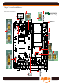
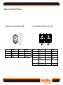
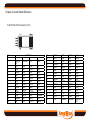
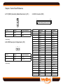
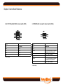
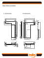
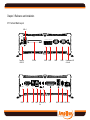
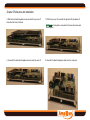
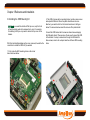
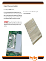
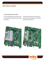
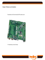
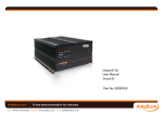
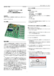
Impact-E20 user manual Part No 85070154 Issue A2 Introduction Impact-E series: The Impact industrial computers incorporate "industrial motherboards" to provide the repeatability and revision control normally associated with SBCs. The new Impact-E range has a small, compact and fanless rugged design, ideally suited to a variety of space-critical embedded applications. Powered by Intel processors, these computers can provide the performance necessary for high speed and intensive tasks. Manufactured from selected high components, the Impact-E series is an ideal cost-effective solution for use in harsh environments and critical 24/7 operations. Introduction Declaration of Conformity CE This product has passed the CE test for environmental specifications when shielded cables are used for external wiring. We recommend the use of shielded cables. Please contact your local supplier for ordering information. Installation Suggestions Ensure you have a stable, clean working environment. Dust and dirt can get into components and cause a malfunction. Use containers to keep small components separated. Adequate lighting and proper tools can prevent you from accidentally damaging the internal components. Most of the procedures that follow require only a few simple tools, including the following: This product has passed the CE test for environmental specifications. Test conditions for passing included the equipment being operated within an industrial enclosure. In order to protect the product from being damaged by ESD (Electrostatic Discharge) and EMI leakage, we strongly recommend the use of CE-compliant industrial enclosure products. A Philips screwdriver A flat-tipped screwdriver A grounding strap An anti-static pad FCC Class A This equipment has been tested and found to comply with the limits for a Class A digital device, pursuant to part 15 of the FCC Rules. These limits are designed to provide reasonable protection against harmful interference when the equipment is operated in a commercial environment. Using your fingers can disconnect most of the connections. It is recommended that you do not use needlenose pliers to disconnect connections as these can damage the soft metal or plastic parts of the connectors. This equipment generates, uses, and can radiate radio frequency energy and, if not installed and used in accordance with the instruction manual, may cause harmful interference to radio communications. Operation of this equipment in a residential area is likely to cause harmful interference in which case the user will be required to correct the interference at his own expense. Handling Precautions 1. Always disconnect the unit from the power outlet whenever you are installing or fixing a component inside the chassis. 2. If possible, always wear a grounded wrist strap when you are installing or fixing a component inside the chassis. Alternatively, discharge any static electricity by touching the bare metal chassis of the unit case, or the bare metal body of any other grounded appliance. 3. Hold electronic circuit boards by the edges only. Do not touch the components on the board unless it is necessary to do so. Do not flex or stress the circuit board. 4. Use the correct screws and do not overly tighten them. 5. Keep the original packaging and static-protective bag in case the unit has to be returned. 3 Chapter 1 ETX Module Reference Chapter 1 ETX Module Reference 1.1 Function Block Diagram Pentium M Processor 478uFCPGA / 479 uFCBGA HOST Bus DDR SO-DIMM INTEL 852-GM CRT out X3 CONNECTOR LVDS Bus GMCH DRAM Bus 732 uFCBGA Hub Bus PCITO ISA BUS ISA X2 CONNECTOR BRIDGE X4 CONNECTOR IDE ICH4 X1 CONNECTOR PCI BUS 421 BGA USBx4 MII INTEL 82562ET LAN X1 X1 CONNECTOR Low Pin Cou nt Bus AC97 (ALC655) FWH SUPER I/O IT8712F/HX QFP 128L COM1/ CO M2 PIO KB/MS IR X3 CONNECTOR Figure 1.1: Function Block Diagram X4 CONNECT OR Chapter 1 ETX Module Reference 1.2 Electrical Specifications Intel® ULV Celeron® M 600 MHz Intel® 852GM + ICH4 chipset Supports one unbuffered nonECC DDR SO-DIMM 200/266 memory up to 1GB Intel® 852GM integrated Graphic, supports both standard VGA and TFT. CRT: Supports up to 1600 x 1200 at 85 Hz; 2048x1536 at 75 Hz DB15 CRT VGA connector x 1 LVDS: Supports up to 48-bit, 1600 x 1200 at 60 Hz Support single/dual pixel LVDS panel Onboard LVDS transmitter for LVDS Interface down to I/O Board. Ethernet: Intel 82562ET 10/100 Fast Ethernet Supports PXE LAN boot function Audio: ALC655 CODEC - AC97 Audio Interface Super I/O: IT8712F ETX Connectors X1 32-bit/33Mhz PCI x 4 Audio CODEC - AC97 Audio Interface USB 2.0 x 4 X2 ISA Interface X3 VGA x 1 LVDS x 1 (Dual Pixels) LPT x 1 KB/Mouse COM1 and COM2 IrDA 1.0 SIR CPU: Chipset: System Memory : Graphics: Ethernet (10/100) SMBus IDE x 2 RTC: On-chip RTC with battery back up / External Li-ion Battery x 1 Located on Carrier Board RTC Tolerance less than 2 secs ( 24 hours ) under 25˚C environment WatchDog: Watchdog timeout programmable by Software from 1 second to 256 seconds. (Tolerance 5% under room temperature 25°C) BIOS: Award System BIOS Advanced Power Management support 4Mbit flash ROM Power Supply: Supports both AT and ATX Power Supply. +5V Power Only, follows ETX power and ground pin definitions. Drivers: Windows 2000/2003, XP, Linux Certifications: CE approval FCC Class A Environment: Operating temperature: 0°C to 60°C (32°F to 140°F) Storage temperature: -20°C to 85°C (-4°F to 185°F ) Relative humidity: Non-operating 5%~95%, non-con densing Dimensions: 95mm (W) x 114mm (L) (3.74” x 4.5”) X4 Chapter 1 Module Reference 1.3 Watchdog Timer Programming Start SetupWDT #Setup Watchdog Timer Environment InitWDT #Initial Watchdog Timer. Users can select second or minute timer at this procedure line 8. SetWDTTime #Set Watchdog Timer Time -out Value. Users can set time- out value at this procedure line .3 ExitSetup #Exit Setup Environment End P.S:Common library ========================================================== === 0 SetupWDT PROC 1 mov al,87h 2 out 2eh,al 3 mov al,01h 4 out 2eh,al 5 mov al,55h 6 out 2eh,al 7 out 2eh,al 8 9 mov al,07h 10 out 2eh,al 11 mov al,07h 12 out 2fh,al 13 ret 14 SetupWDT ENDP ========================================================== === 0 InitWDT PROC 1 mov al,71h 2 out 2eh,al 3 mov al,30h 4 out 2fh,al 5 6 mov al,72h 7 out 2eh,al 8 mov al,0c0h -Here!! set 0c0h for second, set 40h for minute 9 out 2fh,al 10 ret Chapter 1 ETX Module Reference 11 InitWDT ENDP ========================================================== === 0 SetWDTTime PROC 1 mov al,73h 2 out 2eh,al 3 mov al,5 -Here!! Set 5 sec.(time out vale: 0x00-0xff) 4 out 2fh,al 5 ret 6 SetWDTTime ENDP ========================================================== === 0 ExitSetup PROC 1 mov al,02h 2 out 2eh,al 3 mov al,02h 4 out 2fh,al 5 ret 6 ExitSetup ENDP ========================================================== === Chapter 1 ETX Module Reference 1.4 Board Layout 3.00 114.00 1.5 Dimensions 4-?6.00 95.00 U3 A M1 B S C R12 4 C10 C43 RN34 RN35 RN36 RN38 RN39 RN40 RN42 RN41 RN31 R131 R132 C111 R237 R236 R235 R233 R232 R230 R120 R229 C171 R207 C163 1 9 8 3 5 4 7 6 2 11 10 12 14 20 19 C93 R116 64 R366 RN54 C180 R367 RN27 C143 R195 R119 C97 C142 C141 R126 R127 39 R107 128 C146 U16 1 38 111.00 R108 C86 R109 R111 C31 C18 L6 13 22 21 R117 C92 C94 AJ AH AF AG AD AE AB AC Y W U V R T AA N P L M J K G H E D B C A F R21 R20 R18 R16 R17 CT2 C115 U5 0.00 C15 C27 A 65 R118 C83 C64 C RN43 14 13 12 11 10 9 8 7 6 5 4 3 2 1 B C96 2 C20 RN37 C89 RN28 C84 RN23 RN24 41 C RN33 R384 L2 Figure 1.2: Top view D 1 R95 R96 C45 2 1 0.00 E C79 C80 102 C81 3 C7 G F C65 C66 5 C61 C62 6 R11 RN14 Super I/O C42 9 8 7 R10 CT4 R1 10 R9 J H RN32 23 L5 39 11 C2 K C245 12 L C78 40 RN30 RN29 M R110 C41 N R113 13 R151 T RN25 42 RN13 C59 R73 R74 C60 RN12 C87 R64 RN26 R63 14 R150 R C82 C40 15 R154 V U C77 R62 C39 C58 17 16 R156 R146 R147 R148 R149 W R114 R61 19 18 R145 Y RN22 RN8 RN9 C57 C38 20 R144 AA C76 C37 21 U1 R3 R4 C56 R60 22 R2 RN10 R59 23 R143 R153 AC AB RN21 RN7 CT3 C36 24 C6 U6 C72 C75 RN11 + C5 U25 R155 R378 R142 P C35 25 R141 C110 C74 C55 26 R139 R140 R133 C73 C54 FB2 4 5 6 7 1 8 9 3 11 13 10 12 2 C30 R48 R43 R46 R40 R39 R38 R35 R37 R34 R32 20 14 16 18 19 17 15 R28 R30 R27 R26 R24 C19 R23 R22 22 21 24 23 26 25 R14 C13 D1 C33 29 28 27 R395 SODIMM C17 C16 3 R19 R15 A 852GM C98 C53 RN6 B R137 R138 R396 RN20 D RN19 C52 RN5 C51 E 1 ICES101 RE V:B 4BKS0101B1X0 MADE INTAIWAN C71 G F R6 RN18 H C9 C4 R393 R392 R379 R389 R387 R388 R390 R29 R31 R33 C21 C22 R42 R44 C R377 RN2 RN4 RN3 C50 C1 J 29 P N M L K J H G F E D C B A U7 R106 C70 L K 30 21 C69 RN17 C49 M ICH4 RN16 R R13 1 20 3 B R97 R98 R99 R100 R101 R102 R103 R104 R105 A R82 R83 R84 R85 R86 R87 R88 R89 R90 C68 R91 R92 C63 RN15 RN1 C48 T P N R8 J1 199 C67 V U R5 R7 4 1 X1 2 200 R71 R72 C47 Y W PCI-ISA Bridge Intel® Celeron® M U4 DIMM1 C46 AB AA FB1 FB13 C91 C219 R80 R81 AD AC C3 C441 C440 R77 AE C8 4-?2.70 4 C217 R76 R78 R79 R68 D3 AF L1 14 C95 C216 RN44 R65 C44 R66 R67 C28 + R53 R54 C32 C29 R49 R50 R41 R36 5 U8 FB14 FB3 R25 13 G D R75 C90 U2 R58 R369 R56 R45 R47 C12 C14 + C11 C26 CT1 C34 C144 R371 R370 R57 R51 C88 + D2 103 C85 18 R275 R263 17 R253 16 R115 15 L4 L3 R52 D4 92.50 Figure 1.3: Dimensions R220 2.50 Chapter 1 ETX Module Reference 1.6 IRQ Assignments 1.7 PCI Device Interrupt and BUS Assignments Interrupt request lines let peripherals communicate with the CPU for the function required. The following list shows the IRQs used. The ETX module supports PCI expansion fully compliant with the PCI specification. Table 1.1: IRQ assignments Table 1.2: PCI device interrupts on board. Chipset Config. BUS / DEVIC/ FUNCTION PCI INT# IRQ0 Timer IRQ1 KBC IRQ2 Iinternal IRQ3 COMA IRQ4 COMB IDSEL Special feature description ETX PCI(1) 0 / 9 /0 ABCD AD19 ETX ETX PCI(2) 0 / 10 /0 BCDA AD20 ETX IRQ5 Parallel Port / Generic ETX PCI(3) 0 / 11 /0 CDAB AD21 ETX IRQ6 FDC ETX PCI(4) 0 / 12 /0 ABCD AD23 ETX DA82562ET 0/ 8 /0 BCDA AD24 10/100 PHY IT8888G 1 / 6 /0 AD22 PCI to ISA BRIDGE IRQ7 Parallel Port / Generic IRQ8 RTC IRQ9 Generic IRQ10 Generic IRQ11 Generic IRQ12 PS/2 Mouse IRQ13 Internal IRQ14 IDE1 IRQ15 IDE2 Chapter 1 ETX Module Reference 1.8 JP1 : ETX Connector (X1)~PCI BUS, AUDIO OUT, USB 2 100 1 99 Pin 1 3 5 7 9 11 13 15 17 19 21 23 25 27 29 31 33 35 37 39 41 43 45 47 49 Definition GND PCICLK2 GND PCICLK0 REQ3# GNT2# REQ2# REQ1# GNT0# VCC SERIRQ AD0 AD1 AD4 AD6 CBE0# AD8 GND AD10 AD11 AD12 AD13 AD14 AD15 CBE1# Pin 2 4 6 8 10 12 14 16 18 20 22 24 26 28 30 32 34 36 38 40 42 44 46 48 50 Definition GND PCICLK3 GND PCICLK1 GNT3# +3V GNT1# +3V NC VCC REQ0# +3V AD2 AD3 AD5 AD7 AD9 GND AUXAL MIC AUXAR NC SNDL ASGND SNDR Pin 51 53 55 57 59 61 63 65 67 69 71 73 75 77 79 81 83 85 87 89 91 93 95 97 99 Definition VCC PAR GPERR# PME# LOCK# TRDY# IRDY# FRAME# GND AD16 AD17 AD19 AD20 AD22 AD23 AD24 VCC AD25 AD28 AD27 AD30 PCIRST# INTC# INTA# GND Pin 52 54 56 58 60 62 64 66 68 70 72 74 76 78 80 82 84 86 88 90 92 94 96 98 100 Definition VCC SERR# NC USB2# DEVSEL# USB3# STOP# USB2 GND CBE2# USB3 AD18 USB0# AD21 USB1# CBE3# VCC AD26 USB0 AD29 USB1 AD31 INTD# INTB# GND Chapter 12 ETX Module Reference 1.9 JP2 : ETX Connector (X2) ~ ISA BUS 2 100 1 Pin 1 3 5 7 9 11 13 15 17 19 21 23 25 27 29 31 33 35 37 39 41 43 45 47 49 99 Definition GND SD14 SD13 SD12 SD11 SD10 SD9 SD8 MEMW# MEMR# LA17 LA18 LA19 LA20 LA21 LA22 LA23 GND SBHE# SA0 SA1 SA2 SA3 SA4 SA5 Pin 2 4 6 8 10 12 14 16 18 20 22 24 26 28 30 32 34 36 38 40 42 44 46 48 50 Definition GND SD15 MASTER# DREQ7 DACK7# DREQ6 DACK6# DREQ5 DACK5# DREQ0 DACK0# IRQ14 IRQ15 IRQ12 IRQ11 IRQ10 IO16# GND M16# OSC BALE TC DACK2# IRQ3 IRQ4 Pin 51 53 55 57 59 61 63 65 67 69 71 73 75 77 79 81 83 85 87 89 91 93 95 97 99 Definition VCC SA6 SA7 SA8 SA9 SA10 SA11 SA12 GND SA13 SA14 SA15 SA16 SA18 SA19 IOCHRDY VCC SD0 SD2 SD3 DREQ2 SD5 SD6 IOCHK# GND Pin 52 54 56 58 60 62 64 66 68 70 72 74 76 78 80 82 84 86 88 90 92 94 96 98 100 Definition VCC IRQ5 IRQ6 IRQ7 SYSCLK REFSH# DREQ1 DACK1# GND DREQ3 DACK3# IOR# IOW# SA17 SMEMR# AEN VCC SMEMW# SD1 NOWS# SD4 IRQ9 SD7 RSTDRV GND Chapter 1 ETX Module Reference 1.10 JP4 : ETX (X3)~VGA, CLK, VIDEO, COM, LPT, IR, MS/KB 2 100 1 Pin 1 3 5 7 9 11 13 15 17 19 21 23 25 27 29 31 33 35 37 39 41 43 45 47 49 99 Definition GND R HSY VSY LVDS_CLKBM LVDS_CLKBP GND LVDS_YBP1 LVDS_YBM1 GND LVDS_YAM3 LVDS_YAP3 GND LVDS_YAM2 LVDS_YAP2 GND LVDS_YAP0 LVDS_YAM0 VCC NC NC BIASON NC NC Pin 2 4 6 8 10 12 14 16 18 20 22 24 26 28 30 32 34 36 38 40 42 44 46 48 50 Definition GND B G DDCK DDDA LVDS_YBM3 LVDS_YBP3 GND LVDS_YBP2 LVDS_YBM2 GND LVDS_YBP0 LVDS_YBM0 GND LVDS_CLKAP LVDS_CLKAM GND LVDS_YAP1 LVDS_YAM1 VCC BLON# DIGON NC NC Pin 51 53 55 57 59 61 63 65 67 69 71 73 75 77 79 81 83 85 87 89 91 93 95 97 99 Definition NC VCC STB# NC IRRX IRTX RXD2 GND RTS2# DTR2# DCD2# DSR2# CTS2# TXD2 RI2# VCC RXD1 RTS1# DTR1# DCD1# DSR1# CTS1# TXD1 RI1# GND Pin 52 54 56 58 60 62 64 66 68 70 72 74 76 78 80 82 84 86 88 90 92 94 96 98 100 Definition NC GND AFD# PD7 ERR# PD6 INIT# GND PD5 SLIN# PD4 PD3 PD2 PD1 PD0 VCC ACK# BUSY PE SLCT# MSCLK MSDAT KBCLK KBDAT GND Chapter 1 ETX Module Reference 1.11 JP3 ETX : Connector (X4)~IDE, LAN, I2C, SMBUS, MISC 2 100 1 99 Pin 1 3 5 7 9 11 13 15 17 19 21 23 25 27 29 31 33 35 37 39 41 43 45 47 49 Definition GND 5V_SB PS_ON PWRBTN# NC RSMRST# NC NC VCC OVCR# EXTSMI# SMBCLK SIDE_CS3# SIDE_CS1# SIDE_A2 SIDE_A0 GND PDIAG_S SIDE_A1 SIDE_INTRQ BATLOW# SIDE_AK# SIDE_RDY SIDE_IOR# VCC Pin 2 4 6 8 10 12 14 16 18 20 22 24 26 28 30 32 34 36 38 40 42 44 46 48 50 Definition GND PWGIN SPEAKER BATT LILED# ACTLED# SPEEDLED# I2CLK VCC NC I2DAT SMBDATA SMBALRT# NC PIDE_CS3# PIDE_CS1# GND PIDE_A2 PIDE_A0 PIDE_A1 GPE1# PIDE_INTRQ PIDE_AK# PIDE_RDY VCC Pin 51 53 55 57 59 61 63 65 67 69 71 73 75 77 79 81 83 85 87 89 91 93 95 97 99 Definition SIDE_IOW# SIDE_DRQ SIDE_D15 SIDE_D0 SIDE_D14 SIDE_D1 SIDE_D13 GND SIDE_D2 SIDE_D12 SIDE_D3 SIDE_D11 SIDE_D4 SIDE_D10 SIDE_D5 VCC SIDE_D9 SIDE_D6 SIDE_D8 NC RXD# RXD TXD# TXD GND Pin 52 54 56 58 60 62 64 66 68 70 72 74 76 78 80 82 84 86 88 90 92 94 96 98 100 Definition PIDE_IOR# PIDE_IOW# PIDE_DRQ PIDE_D15 PIDE_D0 PIDE_D14 PIDE_D1 GND PICD_D13 PICD_D2 PIDE_D12 PIDE_D3 PIDE_D11 PIDE_D4 PIDE_D10 VCC PIDE_D5 PIDE_D9 PIDE_D6 CBLID_P PIDE_D8 SIDE_D7 PIDE_D7 HDRST# GND Chapter 1 ETX Module Reference 1.12 Impact-E 20 Power Consumption Impact-E 20 System Comprised of ETX Module + Carrier Board Table 1.3: Impact-E 20 power consumption System Configuration Model Name OS Memory Storage CPU AP Impact-E 20 Win XP 1G non-ECC, nonregistered DDR SODIMM 333 memory 40GB Intel ULV Celeron® M 600 MHz K Power + Burning Test Value Power Consumption Theoretical Current * 32.326W Real Current One** 15.84 ~ 16.56W Real Current Two*** 16.32 ~ 17.52W Real Current Three**** 12.72 ~ 12.96W Note: *Theoretical Current means R&D designed power consideration with Onboard Devices ( Does not consider the Add-On devices ) **Real Current One means system with Maximum HD/CPU and Memory Loading/Usage under room temperature. ***Real Current Two means system with 25% HD/70% CPU and 50% Memory Loading/Usage under room temperature. ****Real Current Three means system without running K Power with OS in idle state under room temperature. Chapter 2 Carrier Board Reference Chapter 2 Carrier Board Reference 2.1 Board Layout COM2/COM1 COM4/COM3 PCMCIA PCI 104 USB 2.0 Programmable LED Power and HDD LED CPLD Programmer Pinhead Battery CF Socket PC/104 NVRAM Socket IDE LVDS VGA Dual 10/100 Ethernet Audio Backlight Power Figure 2.1: Board Layout LPT USB 2.0 KB/MS DC In (9 - 36V) Chapter 2 Carrier Board Reference 2.2 Jumpers and Switches JP6 NOTE: Jumpers and Switches are not shown at default settings. 1 JP8 1 3 1 JP7 3 Indicates Pin 1 1 LED2 R276 C118 C257 R72 R76 C1 C2 U13 8 R122 U14 C260 R292 5 CON4 R121 U20 BAT1 R79 C254 R294 R32 R56 C46 C83 R63 C41 R27 C39 R21 R18 C54 C51 R12 R83 R64 R239 C116 RN18 C61 C59 C57 C56 C55 C52 C50 C48 FB12 FB11 R77 2 3 1 2 BZ1 3 D4 1 X2 3 D3 R123 R269 D19 C19 1 FB15 C64 50 25 R41 R34 C74 R51 R234 R38 R36 R42 C69 26 C76 C70 R240 R52 R43 R233 R50 C73 C66 Q1 E R120 C115 R265 3 R66 R126 R124 C C147 R65 C14 B R127 R125 HIGH=1.2mm C77 CE6 D L5 2 C148 R278 R105 R104 R100 R103 C95 R101 R102 R99 HIGH=2mm R93 C91 R94 R89 R178 R189 JP5 1 3 4 2 IDE2 C6 JP5 R272 C7 1 A32 R82 R81 R80 R78 R62 R60 R59 R58 R57 FB14 C63 C62 R290 R289 4 B32 X1 R128 R85 C67 CT8 A2 1 4 SW6 U15 SW2 3 C4 3 R160 R73 U12 U29 1 C13 C82 U11 R45 C256 R293 3 R98 JP7 C72 CT7 A1 U10 R96 1 U6 SW7 U33 R70 R54 R291 C45 C49 R14 R20 JP6 SW9 C R69 R71 C75 C255 R53 R55 C42 C40 2 1 U4 J4 C71 R48 R23 R11 R241 R242 SW10 R46 U32 P2 LED1 R49 P1 FB9 A2 C31 C29 C27 C25 C23 C21 C19 C18 C2 C68 A1 JP8 R161 C1 U19 5 R191 C119 R169 6 C8 R1 1 C78 35 C9 CN3 CE8 1 1 34 68 C CE5 C10 R67 C15 R2 R74 J8 R68 L6 R75 C 2 C79 SW3 C11 D0 C0 C16 D S G C117 SW4 SW5 E X3 U17 R109 M2 D R129 2 U18 5 3 2 FB25 CE10 L R111 R112 R113 FB22 R107 FB21 3 F3 C99 R119 C112 3 R116 3 FB19 CP4 C101 FB20 RN9 R95 CP3 FB23 FB24 C107 C109 C104 C106 C108 FB26 C111 C110 4 FB27 C114 CE4 CE9 C113 8 J7 J5 R115 R110 L1 L2 1 4 1 4 C94 CP2 R91 RN6 R92 CP1 1 D1 6 FB18 CE2 FB17 CE1 J3 C88 J6 9 + 10 CN2 + R254 R255 R252 R248 R247 1 2 11 C98 R97 C85 R61 R243 FB13 R29 FB10 C38 C36 FB7 C30 FB5 C26 FB3 C22 FB8 C34 C32 R7 R8 R5 R3 9 S 1 A1 B1 RN7 JP4 RN5 C103 C97 RN3 L 1 U16 C86 C44 C43 C37 10 C100 RN8 J2 U5 1 2 11 R114 C102 RN4 U8 U7 M CE7 R246 R87 C243 C247 FB16 C246 C242 C250 R284 FB4 R232 C17 C12 C5 CON1 R86 C80 C249 R39 R28 R26 R25 R24 R22 R19 R17 R16 R15 R13 C35 C33 R10 R9 U3 2 RN1 2 C53 G R117 C87 C58 R31 C47 C28 FB6 C24 FB2 C20 F C221 R209 RN2 44 FB1 3 1 2 F1 JP9 J1 IDE1 43 U1 1 R84 9 C81 R275 R273 R274 F 6 R245 R221 M SW8 U R106 C227 F8 E Q3 R108 C B R118 C244 C245 R280 R281 C248 C251 R286 CE3 CT6 C120 Q2 R282 R285 R283 R287 C B CT5 C105 CON3 1 CN1 8 2 8 2 7 1 7 1 4 J CON2 SW1 1 JP9 3 JP4 1 9 3 Chapter 2 Carrier Board Reference 235.00 240.00 215.73 220.00 171.90 130.00 103.00 105.00 65.00 5.00 15.00 28.00 2.3 Carrier Board Dimensions 170.00 COM1 R121 C83 C116 1 R77 BZ1 A32 B32 R81 JP5 R272 GND OUT E/D 126.20 D4 3 1 123.66 R82 R80 VDD 1 2 R78 4 R128 R64 R85 13 12 X2 3 1 C Q1 E C115 R120 R126 R124 R66 R265 C14 R123 D3 C147 R65 D19 PD30 C76 R269 C19 B C70 R240 R52 R43 R233 R50 C73 C66 PA30 1 FB15 C64 R41 R34 50 25 C74 R51 R234 R38 R36 R42 C69 26 C6 R122 R79 C254 R63 R83 R62 R60 R59 R58 R57 VDD E/D C63 FB14 C62 76 C3 R276 C118 JP8 U14 R32 R294 1 75 51 IDE2 C260 U13 R21 R18 C54 C51 R12 RN18 C61 C59 C57 C56 C55 C52 C50 C48 FB12 FB11 R290 R289 4 50 150.00 25 48 2 3 A2 U20 24 13 12 A OUT C257 R72 R76 R292 R56 24 C72 X1 5 CON4 BAT1 36 37 48 C67 2 GND C2 SW6 8 25 R239 3 B R127 R125 C4 C82 U11 26 CT8 C1 1 4 R73 37 100 B 1 C13 R69 R71 C75 1 SW2 CT7 SW7 R160 A1 U15 U12 36 U29 25 U6 C41 C39 R27 SW9 C255 R53 R55 C256 R45 C46 R293 3 R98 JP7 LED2 3 U10 R96 1 U33 R70 R54 R291 10 JP6 9 1 U4 C71 R48 A 2 1 R161 10 J4 R46 1 6 1 1 U32 C45 C49 R14 R20 R23 R11 R241 R242 150.00 SW10 9 5 P2 R49 LED1 6 C42 C40 FB9 A2 C31 C29 C27 C25 C23 C21 C19 C18 C2 5 P1 C68 A1 COM3 COM4 COM2 9 C1 C7 C77 CE6 L5 D2 C148 R105 R104 R278 R103 R102 R101 R100 C95 R99 R94 R93 C91 R89 R178 R189 U19 5 C119 R191 R169 6 C8 R1 1 C78 CE5 35 C9 CN3 CE8 1 34 68 C1 C10 R67 C15 R2 R74 J8 R68 L6 R75 C2 C79 SW3 C11 C F8 E B 2 U18 5 32 FB25 R111 R112 C106 FB23 C107 3 R113 C141 C143 C108 C110 C113 FB24 FB26 FB27 C109 C111 C114 CE4 CE9 8-?8.00 8 4 6 4 14 2 1 5 2 J9 1 3 SW1 CON3 207.00 187.00 147.00 111.00 96.00 79.00 59.00 CON2 228.00 235.00 11 32.00 0.00 5.00 8.00 15 25.00 CE10 R116 4 1 25 + C99 L4 CP4 D16 1 R297 R299 R298 R140 1 7 41 C105 C104 FB22 FB21 2 1 3 RN9 C101 CP3 FB20 CP2 8-?3.60 R119 R109 JP4 L2 F3 RN6 13 1 8 L1 J7 46.19 R129 A1 C100 CP1 1 J5 D1 6 R92 CE2 FB19 C5 2 CE1 J3 R91 J6 9 FB18 10 D L9 C156 R115 R107 R110 C98 U17 11 CN2 LAN1 L3 1 C88 12 C166 C97 U16 RN7 R97 R95 C94 C86 C85 9 B1 C87 RN8 FB17 10 M2 C264 1 + C17 C12 5 2 J2 19 RN5 R61 11 CN1 LAN2 8 1 7 CON1 1 19 + R254 R255 12 R252 U5 R243 FB13 R29 R248 R247 R7 R8 R5 R3 FB1 20 RN3 M1 S CE7 R245 C44 C43 U1 U8 U7 C221 RN4 RN2 RN1 C58 R31 C53 FB10 C38 C36 FB7 C30 FB5 C26 FB3 C22 FB8 C34 C32 U3 R87 C47 C28 FB6 C37 F2 R221 C247 FB4 R10 R9 F1 R232 0.00 2 G C227 R209 2 J1 20 1 44 C24 FB2 C20 U2 C243 FB16 C246 C242 C250 R284 R39 IDE1 43 3 R86 C80 C249 R28 R26 R25 R24 R22 R19 R17 R16 R15 R13 C35 C33 SW8 20.00 1 R84 M6 JP9 C81 R275 R273 R274 40.00 F9 R246 Q3 R118 CT6 X3 50.00 4-?3.20 C244 C245 R280 R281 C248 C251 R286 CT5 G CE3 SW5 SW4 S C117 PA1 PD1 E D C120 Q2 R282 R285 R283 R287 4-?6.50 C B D0 C0 C16 Chapter 2 Carrier Board Reference 2.4 Impact-E20 Specifcations IDE Internal CompactFlash socket x 1 ( Primary IDE ) External Access Compact Flash Socket x 1 ( Secondary IDE ) 44-pin IDE Connector x 1 (Primary IDE ) COM Ports COM 1 ~ 2 from ETX Module support RS232 COM 3 ~ 4 via ISA Interface, support RS422/485 Automatic RS-485 data flow control Optical Isolation, Max 2KV ±15KV ESD protected 10-pin Screw Terminal Connector ( Pin assignment: TBD ) Speed: RS-422/485: 50 ~ 921.6 Kbps USB 2.0 USB 2.0 Ports x 2 in the Front USB 2.0 Ports x 2 in the Rear PIO LPT Port x 1 ; 25-pin D-type supporting bi-directional, EPP and ECP modes Audio From ETX Module: Audio Out Mic In Graphics From ETX Module: Internal LVDS Interface Hirose DF13-20DP x 2 for Dual Pixels LVDS External Display Interface by Analog CRT DB15 VGA Con nector Ethernet From ETX Module: 10/100 Fast Ethernet, RJ45 with LED connector x 1 Carrier Board with On Fast Ethernet LAN Chip VIA VT6105 via PCI Interface. RJ45 with LED Connector x 1 Expansion PC/104-Plus ( ISA+PCI) x 1 PCMCIA Socket x 1 Supports CardBus 32-bit and 16-bit cards Power Supply On-board DC to DC circuit support Power Input Range from +9V to +36VDC. Standard Configuration for NICE 3200 series models is +24VDC Input WARNING: If you use 9V~12V voltage, please change the JP4 to 1-2, and not +12V and -12V power output. Default JP4 is 3-4 while you use 13V~36V voltage. Chapter 2 Carrier Board Reference LED and Others On-board buzzer One Reset Switch and Power LED and CF/HDD status LED Two LEDs Connect to GPIO, that is programmable for Alarm or other purposed defined by developer. Provide User Inter face Utility of Windows 2K/XP and Linux for user to config ure the Alarm Status of Thermal or Voltage status on the front LEDs. Operating temperature: SRAM -20°C to +60°C (-4°F to 140°F) Reserved NVRAM Socket for the Optional 512 KB battery backed SRAM (NVRAM ) Chapter 2 Carrier Board Reference External Connectors for Impact-E20 2.5 CompactFlash Connector IDE2 (Slave), IDE3 (Master) 50 49 26 1 Pin No. 1 3 5 7 9 11 13 15 17 19 21 23 25 Description Gnd Data 4 Data 6 HDC CS100 Gnd Gnd +5V Gnd Gnd Disk Address 1 Data 0 Data 2 CF_CD2# (Pull-down) Pin No. 2 4 6 8 10 12 14 16 18 20 22 24 26 Description Data 3 Data 5 Data 7 Gnd Gnd Gnd Gnd Gnd Disk Address 2 Disk Address 0 Data 1 IOCS16# (NC) CF_CD1# (Pull-down) 27 29 31 33 35 37 39 41 43 45 47 49 Data 11 Data 13 Data 15 CF_VS1# (NC) IOW Interrupt 15 CF_CSEL# (Master or Slave) Reset # DMA REQ / DACK (NC) 28 30 32 34 36 38 40 Data 12 Data 14 HDC CS300 IOR CF_WE# (+5V) +5V CF_VS2# (NC) 42 44 HDD Active Led Data 8 Data 10 46 IOCHRDY DMA ACK# /CF_REG# (+5V) DMA66 Detect / CF_PDIAG# Data 9 Gnd 48 50 Chapter 2 Carrier Board Reference 2.6 SIO connector COM1(P1),COM2(P2) 4.7 RS422/485 COM3,COM4(J4)~COM3 : IRQ10 , COM4 : IRQ5 The Impact-E20 provides two D-sub 9-pin connectors, which offers standard 232 serial communication interface port of COM1/COM2. 1 2 5 3 4 1 2X 2X 4X 4X 2X 2X 4X 4X 10 #/- 6 7 8 Pin 2 Definition Serial Input 3 Definition Data Carrier Detect# Serial Output 4 5 Chassis Gnd 6 7 Request To Send# Ring Indicator# 8 Data Terminal Ready# Data Set Ready# Clear To Send# Pin 1 9 #/- 9 Pin Definition Pin Definition 1 COM3/ RS422/485 TX+ 2 COM3/ RS422/485 TX- 3 COM3/RS422 RX+ 4 COM3/RS422 RX- 5 Gnd 6 COM4/ RS422/485 TX+ 7 COM4/ RS422/485 TX+ 8 COM4/RS422 RX+ 9 COM4/RS422 RX- 10 Gnd Chapter 2 Carrier Board Reference 2.9 VGA connector ( CON1) 2.8 PIO connector ( J7) 14 25 5 1 10 1 Pin 1 3 5 7 9 11 13 15 17 19 21 23 25 Definition Line Print Strobe Parallel Data 1 Parallel Data 3 Parallel Data 5 Parallel Data 7 BUSY Select Error Select input Chassis Gnd Chassis Gnd Chassis Gnd Chassis Gnd Pin 2 Definition Parallel Data 0 4 6 8 10 12 14 16 18 20 22 24 26 Parallel Data 2 Parallel Data 4 Parallel Data 6 Acknowledge Paper empty Auto feed Initialize Chassis Gnd Chassis Gnd Chassis Gnd Chassis Gnd Chassis Gnd 6 15 13 Pin 1 3 5 7 9 11 13 15 Definition RED BLUE Gnd Gnd KEY NC Hsync ID3 11 Pin 2 4 6 8 10 12 14 Definition GREEN NC Gnd Gnd Gnd ID1 Vsync Chapter 2 Carrier Board Reference 2.10 Keyboard + mouse connector ( CON3 ) 2.11 LAN connector ( CN2,LAN1 : CN1, LAN2 ) Pin 6 Pin 5 Pin 4 Pin 3 Pin 2 Pin 1 Pin 1 3 5 Definition KBDataGnd KBClk Pin 2 4 6 Definition MouseData VCC MouseClk Pin 1 3 5 7 9 11 • • • • •• • • • • • • •• • • LAN1 LAN2 Definition TX+ RX+ LAN1 LAN2 LAN Speed LED LAN Link LED Pin 2 4 6 8 10 Definition TXLAN1 RXLAN2 Vcc3 12 LAN ACT LED# Chapter 2 Carrier Board Reference 2.12 Line out connector ( J3 ) Pin 1 3 5 Definition Gnd SNDR Gnd 2.14 USB connector ( CON2:USB0/1,CON4:USB2/3 ) Pin 2 4 Definition SNDL Gnd Pin No. 1 3 5 7 2.13 MIC connector ( J5 ) Pin 1 3 5 Definition Gnd VCC5 Gnd Pin 2 4 Definition MIC_IN Gnd Description VCC5 USB+ VCC5 USB1+ Pin No. 2 4 6 8 Description USBUSB Gnd USB1USB Gnd Chapter 2 Carrier Board Reference 2.15 PCMCIA connector ( CN3) 1 Pin 1 2 3 4 5 6 7 8 9 10 11 12 13 14 15 16 17 Definition Gnd D3 D4 D5 D6 D7 CE1# A10 OE# A11 A9 A8 A13 A14 WE# Ready Vcc 68 Pin 35 36 37 38 39 40 41 42 43 44 45 46 47 48 49 50 51 Definition Gnd CO1# D11 D12 D13 D14 D15 CE2# VS1 IORD# IOWR# A17 A18 A19 A20 A21 Vcc 18 19 20 21 22 23 24 25 26 27 28 29 30 31 32 33 34 VPP A16 A15 A12 A7 A6 A5 A4 A3 A2 A1 A0 D0 D1 D2 WP Gnd 52 53 54 55 56 57 58 59 60 61 62 63 64 65 66 67 68 VPP A22 A23 A24 A25 VS2# Reset WAIT# INPACK# REG# BVD2 BVD1 D8 D9 D10 CO2# Gnd Chapter 2 Carrier Board Reference 2.16 System RESET Select Switch (SW8) 2.18 GPIO LED I/O PORT Address & DATA A1 Pin Definition 1~4 Power Good in* 2~3 Resume Reset A2 LED No. * default setting Function Description A1 — I/O PORT Address : EEEH DATA : 01H(LIGHT) 02H(DART) A2 —I/O PORT Address : EEEH DATA : 04H(LIGHT) 08H(DART) 2.17 DC Power input Voltage ( J9 ) 2.19 POWER ON & IDE Active LED (LED2) 072 6 $#). Pin No. Function Description 1 GND 2 +9V~+36V DC INPUT ($$ Chapter 2 Carrier Board Reference Internal Connectors for Impact-E20 2.20 VRAM PIN Defined(U16) U16 1 2 3 4 5 6 7 8 9 10 11 12 13 14 15 16 1 2 3 4 5 6 7 8 9 10 11 12 13 14 15 16 32 31 30 29 28 27 26 25 24 23 22 21 20 19 18 17 32 31 30 29 28 27 26 25 24 23 22 21 20 19 18 17 1X16_2.54MM Pin No. 1 2 3 4 5 6 7 8 9 10 11 12 13 14 15 16 Description ISA A18 ISA A16 ISA A14 ISA A12 ISA A7 ISA A6 ISA A5 ISA A4 ISA A3 ISA A2 ISA A1 ISA A0 ISA D0 ISA D1 ISA D2 GND Pin No. 17 18 19 20 21 22 23 24 25 26 27 28 29 30 31 32 Description ISA D3 ISA D4 ISA D5 ISA D6 ISA D7 ROM CS# ISA A10 BMEMR# ISA A11 ISA A9 ISA A8 ISA A13 BMEMW# ISA A17 ISA A15 +5V Chapter 2 Carrier Board Reference 2.21 PC/104-PLUS connector ( J8A~ISA ) D19 C19 D0 C0 A32 B32 Pin D C 0 GND GND 1 MEMCS16* SBHE* 2 IOCS16* LA23 3 IRQ10 LA22 4 IRQ11 LS21 5 IRQ12 LS20 6 IRQ15 LS19 7 IRQI4 LA18 8 DACK0* LA17 9 DRQ0 MEMR* 10 DACK5* MEMW* 11 DRQ5 SD8 12 DACK6* SD9 13 DRQ6 SD10 14 DACK7* SD11 15 DRQ7 SD12 16 +5V SD13 17 MASTER* SD14 18 GND SD15 19 GND GND/KEY A1 B1 Pin 1 2 3 4 5 6 7 8 9 10 11 12 13 14 15 16 17 18 19 20 21 22 23 24 25 26 27 28 29 30 31 32 A IOCHCK* D7 D6 D5 D4 D3 D2 D1 D0 IOCHRDY AEN A19 A18 A17 A16 A15 A14 A13 A12 A11 A10 A9 A8 A7 A6 A5 A4 A3 A2 A1 A0 GND B GND RSTDRV +5V IRQ9 N/A DRQ2 -12V ENDXFR* +12V GND/KEY SMEMW* SMEMR* IOW* IOR* DACK3* DRQ3 DACK1* DRQ1 REFRESH* SYSCLK IRQ7 IRQ6 IRQ5 IRQ4 IRQ3 DACK2* TC BALE +5V OSC GND GND Chapter 2 Carrier Board Reference 2.22 PC/104-PLUS connector ( PCI ) Pin 1 2 3 4 5 6 7 8 9 10 11 12 13 14 A Gnd/5.0V KEY VI/O AD05 C/BE0# Gnd AD11 AD14 +3.3V SERR# Gnd STOP# +3.3V FRAME# Gnd Definition B C Reserved +5V D AD00 AD02 Gnd AD07 AD09 VI/O AD13 C/BE1# GND PERR# +3.3V TRDY# Gnd AD16 +5V AD03 AD06 Gnd M66EN AD12 +3.3V PAR SDONE Gnd DEVSEL# +3.3V C/BE2# AD01 AD04 Gnd AD08 AD10 Gnd AD15 SB0# +3.3V LOCK# Gnd IRDY# +3.3V 15 16 17 18 19 20 21 22 23 24 25 26 27 28 29 30 AD18 AD21 +3.3V IDSEL0 AD24 Gnd AD29 +5V REQ0# Gnd GNT1# +5V CLK2 Gnd +12V -12V +3.3V AD20 AD23 Gnd C/BE3# AD26 +5V AD30 Gnd REQ2# VI/O CLK0 +5V INTD# INTA# Reserved AD17 Gnd AD22 IDSEL1 VI/O AD25 AD28 Gnd REQ1# +5V GNT2# Gnd CLK3 +5V INTB# Reserved Gnd AD19 +3.3V IDSEL2 IDSE;3 Gnd AD27 AD31 VI/O GNT0# Gnd CLK1 Gnd RST# INTC# Gnd/3.3V KEY Chapter 2 Carrier Board Reference 2.23 DC Adapter Input Voltage Select ( JP4 ) 2.25 CPLD Programmer PIN Header(JP6) 1 JP4 JP6 3 1 Pin No. Status Function Description Pin Definition Pin Definition 1-2 Short 9V-12V (NO +12V and -12v) 1 TCK 2 GND 3 TDO 4 +3.3V 2-3 Short* 13V-36V 5 TMS 6 N/A * default setting 7 N/A 8 N/A 9 TDI 10 +3.3V * default setting 2.24 CMOS Input Voltage Select ( JP5 ) 1 2.26 CF(IDE2) Primary Master/Slave Select ( JP7 ) JP5 3 1 Pin No. Status Function Description Pin No. Status JP7 3 Function Description 1-2 Short* VBAT IN 1-2 Short* Slave 2-3 Short Clear CMOS 2-3 Short Master * default setting * default setting Chapter 2 Carrier Board Reference 2.27 CF(IDE3) Secondary Master/Slave Select ( JP8 ) 2.29 IDE Connector (IDE1) 1 44 1 43 JP8 2 3 Pin No. Status Function Description 1-2 Short Slave 2-3 Short* Master * default setting 2.28 LVDS Power input Voltage Select ( JP9 ) 1 JP9 3 Pin No. Status Function Description 1-2 Short +5V IN 2-3 Short* +3.3V IN * default setting Pin 1 3 5 7 9 11 13 15 17 19 21 23 25 27 29 31 33 35 37 39 41 43 Definition RstdrvIded7 Ided 6 Ided 5 Ided 4 Ided 3 Ided 2 Ided 1 Ided 0 Gnd IdereqIdeiowIdeiorIderdy IdeackIdeirq DA1 DA0 SCS1 IdeactVCC5 Gnd Pin 2 4 6 8 10 12 14 16 18 20 22 24 26 28 30 32 34 36 38 40 42 44 Definition Gnd Ided 8 Ided 9 Ided 10 Ided 11 Ided 12 Ided 13 Ided 14 Ided 15 NC Gnd Gnd Gnd IDE-PD1 Gnd NC 66 Detect DA2 SCS3 Gnd VCC NC Chapter 2 Carrier Board Reference 2.30 LVDS connector ( J1,J2) LVDS connector J2 LVDS connector J1 Pin 1 3 5 7 9 11 13 15 Definition LVDS_CLK Panel_VDD LVDS_9 LVDS_8 GND LVDS_7 LVDS_6 GND Pin 2 4 6 8 10 12 14 16 17 LVDS_5 18 19 LVDS_4 20 Definition LVDS_DAT LVDS_1 LVDS_0 Panel_VDD LVDS_3 LVDS_2 GND Panel_backlight Panel_backlight GND Pin 1 3 5 7 9 11 13 15 Definition LVDS_CLK Panel_VDD LVDS_19 LVDS_18 GND LVDS_17 LVDS_16 GND Pin 2 4 6 8 10 12 14 16 17 LVDS_15 18 19 LVDS_14 20 Definition LVDS_DAT LVDS_11 LVDS_10 Panel_VDD LVDS_13 LVDS_12 GND Panel_backlight Panel_backlight GND 2.31 COM3(SW9),COM4(SW10) IRQ Select switch COM3(SW9) Pin 1~8 2~7 3~6 4~5 * default setting Definition IRQ12 IRQ10* IRQ5 IRQ6 COM4(SW9) Pin 1~8 2~7 3~6 4~5 Definition IRQ12 IRQ10 IRQ5* IRQ6 Chapter 2 Carrier Board Reference 2.32 R5C485(U27) IDSEL Select switch (SW6) SW6 Pin 1~8 2~7 3~6 4~5 * default setting Definition AD19* AD23 AD27 AD31 2.33 PC/104-PLUS (J8B) IDSEL Select switch (SW4,SW5) IDSEL0(SW4) Pin 1~8 2~7 3~6 4~5 * default setting Definition AD16 AD20* AD24 AD28 IDSEL1(SW5) Pin 1~8 2~7 3~6 4~5 Definition AD17 AD21* AD25 AD29 Chapter 2 Carrier Board Reference 2.34 VT6105G(U28) IDSEL Select switch (SW3) SW3 Pin 1~8 2~7 3~6 4~5 * default setting Definition AD18 AD22 AD26* AD30 2.35 RS485/422 Autoswitch Select switch (SW2) SW2 Pin 1~4 COM3* 2~3 COM4* * default setting Definition ON : RS422 Slave and RS485 Autodetect and Autoswitch OFF : RS422 Master ON : RS422 Slave and RS485 Autodetec and Autoswitch OFF : RS422 Master Chapter 3 Reference and Installation Chapter 3 Reference and Installation 3.1 Packing List for Impact-E Series 3.2 Specifications CD with driver and user manual x1 IDE cable x 1 PS/2 keyboard/mouse cable x 1 2-pin power terminal block x1 10-pin RS422/485 terminal block x1 Construction: Dimensions: Main board: Main memory: Aluminum chassis with fanless design 195mm (W) x 268mm (D) x 80mm (H) ICES120 One 200-pin SODIMM socket for up to 1GB NonECC Non-Registered DDR SDRAM memory Device: On-board CompactFlash socket x 2 (internal x 1, external x 1) On-board CompactFlash socket x 1 Internal 2.5” HDD Drive bay x 1 Front I/O Ports: Power / HDD Status LEDs 2 LEDs, connect to GPIO, programmable for Alarm or other purpose defined by developer PCMCIA Socket x 1 DB9 COM1 and COM2 Screw Terminal COM3 and COM4 External access CompactFlash Socket (2nd Com pactFlash available NICE 3200 only) USB 2.0 x 2 Rear I/O Ports: RJ45 with LED connector x 2 USB 2.0 Ports x 2 KB Mouse connector +24V DC Power Input Optional: Power Adapter (65W, 19V) (w/US type power cord) x 1 Power Adapter (65W, 19V) (w/Schuko type power cord) x 1 Power Adapter (65W, 19V) (w/UK type power cord) x 1 Impact-E Expansion DIY Kit P/N: 602D00CD89X0 P/N: 60233IDE54X0 P/N: 60233MK202X0 P/N: 4NCPF00204X0 P/N: 4NCPF01002X0 P/N: 7400065001X0 P/N: 7400065002X0 P/N: 7400065003X0 P/N: 5060900046X0 If any of these items are missing or damaged, please contact Amplicon immediately. While unpacking, check for signs of shipping damage. (For example, damaged box, scratches, dents, etc.) If it is damaged or it fails to meet the specifications, notify our service department or your local sales representative immediately. Also notify the carrier. Retain the shipping carton and packing material for inspection by the carrier. After inspection, we will make arrangements to repair or replace Chapter 3 Reference and Installation Power Reset Button VGA Connector (DB15) Audio Out and Mic In Connector. LPT Port x 1 Expansion Slots: PCMCIA Slot x1: Supports CardBus 32-bit and 16-bit cards PC/104-Plus (ISA+PCI): Supports ISA device x1 / PCI device x2 NVRAM Socket Power Supply: DC to DC power design on-board support 9V DC ~ 36V DC (Max. 50W) Optional External 65W AC adapter x1 NOTE: If you use 9V~12V voltage, please change the JP4 to 1-2, and no +12V and -12V power output. Default JP4 is 3-4 while you use 13V~36V voltage. Environment: Operating Temperature: Storage Temperature: Relative Humidity: Certifications: Software: Ambient with air: 5° C to 40° C (HDD)(41° F to 104° F) -10° C to 50° C (CF)(14° F to 122° F) Tcase ( Surface Temperature of Chassis) 5° C ~ 45° C (HDD) (41° F to 113° F) -10° C ~ 50° C (CF) (14° F to 122° F) -20° C to 80° C (-4°F to 176° F) 10% to 90% (Non-condensing) CE approval /FCC Class A WIndows® XP, WIndows® 2000/2003, Linux Chapter 3 Reference and Installation 3.3 Dimensions CF HDD COM4 Rx- Rx+ Tx- Tx+ PWR COM3 COM2 COM1 A2 Rx- Rx+ Tx- Tx+ PCMCIA A1 - 55.00 61.00 + RESET VGA Amphenol Amphenol LAN1 LAN2 KB/MS +24V DC IN 172.00 92.00 260.00 132.00 176.00 172.00 132.00 92.00 284.00 272.00 Chapter 3 Reference and Installation 3.5 Heatsink Dimensions 114.01 111.01 114.00 111.00 6.00 3.00 6.00 3-螺柱:內孔3mm L:8mm 3.00 50.00 96.00 93.00 96.00 76.00 93.00 96.00 3-螺柱:內孔3mm L:8mm 2.70 1.20 3.00 15.00 3.00 3.00 20.00 12.00 3.00 3.4 Heatsink Dimensions 6.00 10.00 6.00 1.20 2.70 6.70 2.70 1.20 38.00 3.00 6.70 65.00 6.90 108.00 8.00 1.50 10.00 48.00 6.00 20.00 65.00 114.00 Chapter 3 Reference and Installation 3.6 Front and Back Layout USB x 2 PCMCIA PWR A1 Rx- Rx+ Tx- Tx+ COM4 HDD Rx- Rx+ Tx- Tx+ COM3 COM2 COM1 A2 CF Power and HDD LED PCMCIA CompactFlash COM4 COM3 COM2 COM1 Programmable LED A1 and A2 + RESET RESET VGA VGA Amphenol Amphenol LAN1 LAN2 LAN1 LAN2 KB/MS Speaker MIC In Out LPT USB x 2 +24V DC IN KB/MS +24V DC IN Chapter 3 Reference and Installation 3.7 Front and Back Layout USB x 2 PCMCIA PWR A1 Rx- Rx+ Tx- Tx+ COM4 HDD Power and HDD LED COM4 PCMCIA Rx- Rx+ Tx- Tx+ COM3 COM3 COM2 COM2 COM1 COM1 A2 Programmable LED A1 and A2 + RESET RESET VGA VGA Amphenol Amphenol LAN1 LAN2 LAN1 LAN2 KB/MS Speaker MIC In Out LPT USB x 2 +24V DC IN KB/MS +24V DC IN Chapter 3 Reference and Installation 3.8 Disassembly Procedures NOTE: If you would like to slide off the top cover only, just the front or back faceplate needs to be removed (only one). For example, to install a HDD you only need to remove the top cover of the chassis. 1. Remove the green COM 3 and COM 4 and Power connectors from front and back cover plate. 3. Remove the front cover plate. 2. Unscrew the 4 screws from the front and back cover plate. 4. Remove the back cover plate. Chapter 3 Reference and Installation 5. With front and back faceplates removed, slide the top cover off from either the front or the back. 7. With the top cover off, now slide the right and left side plates off. NOTE: Each side plate is connected to the base with a male and female groove 6. View with front and back faceplates removed, and top cover off. 8. View with front/back faceplates, sides and cover removed. Chapter 3 Reference and Installation 3.9 Installing the HDD Mounting Kit NOTE: If you would like to slide off the top cover, only the front or back faceplate needs to be removed (only one). For example, for installing a HDD you only need to remove the top cover of the chassis. With front and back faceplates and top cover removed, it would be the correct time to install the HDD kit if you wanted. 1. First, locate the HDD mounting holes on the carrier board as shown below. 2. The HDD kit comes with a mounting bracket, a cable, some screws and a plastic EMI shield. Since the plastic shield does not come attached, you need to stick it on the bracket as shown in the figure below. The same red arrows mark the corners of the plastic shield. Connect the HDD bracket with 4 screws as shown below and apply the EMI plastic shield. There are also 4 holes used to mount the HDD to the bracket. It is okay to make holes through the EMI shield for these screws, since it will overlap at least two of these HDD mounting holes. Chapter 3 Reference and Installation 3.10 Continuing the Disassembly 1. With front and back faceplates and top cover removed, to continue with the disassembly remove the 8 screws holding the carrier board to the chassis base. 2. After removing the carrier board, flip the board over to find the ETX module with heatsink. Chapter 3 Reference and Installation 3.11 Installing SODIMM Memory At this point, now would be the time to change the memory if you wanted. Please remember that your comes with memory preinstalled Install the memory just as you would regularly SODIMM. Line up the memory pins correctly coming in at an angle, start the pins and push in and down until the sides of the memory snaps into the clip. WARNING: When you install memory into the socket, make sure to tilt it 45 degrees and then slide it in. Be sure to read the memory installation instructions to prevent damaging the memory during installation. The chassis base shown below. Notice the 8 supports to mount the carrier board. Chapter 3 Reference and Installation 3.12 Removing the ETX Module and Heatsink 1. To remove the heatsink and ETX module, remove the 4 screws at the corner of the ETX module. Please note these same 4 screws also secure the heatsink. 2. With the ETX module mounting screws removed, simply pull up on the module on four corners to pop the module out of the four ETX sockets that connect to the carrier board. Chapter 3 Reference and Installation The backside view of the carrier board with ETX module removed. 3. To reassemble, just reverse the steps.