1
INTRODUCTION
This documentation contains information on how to create your own models for use with Proteus
VSM. It is aimed at advanced users of the system and assumes knowledge of how to create
schematics and run simulations with ISIS and PROSPICE. We also assume that you have the
necessary knowledge of electronics to design simulator models that correctly emulate the
behaviour of the parts that you want to use. This is not always a trivial matter, and much of the skill
involves judging what approximations it is legitimate to make.
For information on the availability of existing models, check out www.labcenter.co.uk. You can
also lodge requests for models to be developed within the VSM Marketplace.
This file was last updated on 30/10/2000.
HOW SPICE WORKS
Introduction
This section contains a very brief overview of how SPICE simulates a circuit. If you are wanting to
create models which involve complex analogue behaviour, you will be well advised to read the
extensive documentation available relating to SPICE3F5 itself.
The following discussion relates exclusively to transient analysis.
Representing the Circuit
The circuit is considered to consist of nodes and branches, where a node is the junction of two or
more branches, and a branch is a simple circuit element. In the technique used by SPICE, only the
node voltages are found. These are sufficient (given a knowledge of the branches) to determine also
branch currents in the cases where this is required.
There are basically three types of circuit element. These are:
• the resistor
• the ideal current source (optionally voltage or current controlled)
• the ideal voltage source (optionally voltage or current controlled)
The circuit, the current state, and the results are all represented using matrix and vector quantities.
For the uninitiated, a vector is a single dimension matrix, or a simple array. At each point of
calculation, the expression
[I][Y] = [V]
is computed. [I] and [V] are vectors, and [Y] is a two-dimensional matrix. Note the similarity to
Ohm's law, since [Y] is a matrix of admittances. This is a representation of a set of simultaneous
equations of the form
IaYa + IbYb + IcYc = V
which are solved to find V. Note that, V is often referred to as the RHS vector, sitting as it does on
the Right Hand Side of the above equation.
For each solution of the matrices (to find [V]) the [I] and [Y] matrices are loaded with values that
correspond to the branches that form the circuit. These values may be set within component
models to particular values that reflect the state of the model. So, it is [I] and [Y] together that form
the circuit description and state, and [V] that forms the result.
From Resistors to Controlled Current and Voltages Sources
A resistor may be though of, in a funny way, as a linear voltage controlled current source in which
the input and output nodes share the same pins. In fact, SPICE can also directly model any linearly
controlled voltage or current source by loading constants into different parts of the [I] and [Y]
matrices.
Another way of thinking about this is to note the fact that placing a number in a particular row and
column of the [Y] matrix indicates that a current flow between those nodes will develop a potential
difference between them. The bigger the number, the bigger the voltage. Any linear relation between
branch currents and node voltages can thus be represented simply by loading constants into the
[Y] matrix, whilst currents flowing into particular nodes can be described by loading values directly
into the [I] vector.
Non-Linearities
We mentioned before 'points of calculation'. How are these points defined? Well, let us first
consider the simple case. If we have a circuit that consists entirely of time-invariant linear branches,
then it takes one matrix solution to find the node voltages ([V]) which are valid for all time. A linear
branch obeys ohm's law, including the cases where R = V = 0 with I constant, and Y = I = 0. This
is, in fact, the only type of circuit that may be solved using the [I][Y] = [V] technique.
So how do we cope with non-linear components, such as diodes and transistors? We produce 'fake'
circuits that coincide with the state of the non-linearities. It can take a while to get to grips with this
concept. Consider a diode in a circuit. Consider that we know already the voltages in the circuit in
its stable state. We know about the diode's state, since we know the transfer function:
qVd
Id = Io exp
− 1
kT
We also know that at the solution values, the resistor has value Vd/Id (Ohm's Law) and the current
source (Is) rests at zero since a diode does not actually produce current. This is best viewed on a
diagram:
Id
Diode Response
(Id=I exp(qVd/kT - 1)
Linearised Model Response
Vd
The very, very clever people who invented SPICE realized that the circuit could be made to converge
towards this solution if, for each iteration we set:
Yr = Id Vd
where Vd is measured from the previous solution and Id is computed from the above equation and
Is = Id −
dId
dVd
Let us see how this works, assuming that the diode is connected through a resistor to a battery.
•
The diode will start life open circuit, and the initial matrix solution will find the full battery voltage
across it. No current will flow.
•
Using the above equations, new values for Yr and Is will be calculated. Yr will be zero, but Is will
be negative because we are at a point somewhere on the right of the graph where the slope is
steep and because Id (from the previous solution) is zero.
•
This new value for Is is loaded into the current source, and the process is repeated.
•
The current source will pull some current through the diode and a voltage drop will develop
across the series resistor. So for this second step, the voltage across the diode will be smaller
and the current through it will have increased from zero. In other words, we have moved nearer
to the solution.
•
If the process is repeated for a few more steps, a situation will arise at which
Id =
dId
dVd
(to a pre-determined tolerance, anyway)
and the contribution from the current source will disappear. At this point, the circuit is said to
have converged.
The mathematically astute amongst you will recognize this as the Newton-Rapheson technique,
and indeed it is. Some extra sophistication is needed to prevent divisions by zero and the like. In
particular, no admittance is ever assigned a value greater than the GMIN system variable.
Time Variance
To complete the picture, we must consider time varying circuits. The time-varying parts of a circuit
are generally capacitors and inductors, although to be accurate we must include some generators
and the mixed mode interface models. Note that diodes and transistors often have capacitors within
their models, and so they are also time dependant.
How do we model a capacitor? Well, like the diode we represent it as a resistor and current source
in parallel. We pick values for them based on the capacitor's voltage and current. This is given by:
Q = CV (or V = Q/C)
and Q = It, or more accurately I = dQ/dt.
Note that a given timepoint, a capacitor is like a battery so this time the current source will not be
zero valued at convergence and that the capacitor model does not need to perform
Newton-Rapheson converging because it is a linear device.
To simulate a circuit with capacitors, we slice the simulation period up into discrete time frames.
For each frame, the capacitors are modelled according to their charge stored at that time frame,
and the 'd.c.' solution of the circuit is found as before. Note that this may involve iterations for each
time frame, if other non-linear components are present.
O.k. so far? Well, we just said that we model the capacitor based on its stored charge. But how do
we know what that is? After the solution of the circuit we know what it should be (since we know Vc
and Q = CVc) but we need the information beforehand in order to find the model to do the
simulation. We do, however, know the history of the capacitor. We know all its values of charge and
current since the simulation started (if we care to store them). So, the find the charge at time t, we
extrapolate the curve of the previous charge values (t -1, t-2 etc.) to get the new value. This is where
the whole business of whether to use Gear or Trapezoidal integration comes in.
There are two things that should be obvious here. Firstly, the time difference between time frames
is a very important parameter. It needs to be small, in order that our extrapolation is accurate, but it
needs to be as large as possible so that overall simulation time is reduced. Also, the answer
gained from our extrapolation is never going to be completely accurate (although it may be very
close indeed). All this leads to stability problems. One way of visualising the problem is this.
Imagine a cliff, which is on the edge of the precipice of instability. Behind is the solid ground of
constant circuit values, the starting conditions. We make a bridge across the void by placing
planks on circuit solutions. We must, however, throw the next plank out before we stand on it. The
further away it is, the harder it is to throw to the right (stable) place. If we overstep the mark, and
throw it too far, then it may appear to be all right, but the following circuit may still fail to reach a
stable solution, or else we may just plunge straight down.
This is a really hard problem. For the pioneers of circuit simulation, this was even harder than
non-linear components. It all comes back to numerical integration (since that is what our
extrapolation is really based on) and Nyquist stability criteria.
The main result of this integration is to find a value for the next time step - how far to throw our
plank. The timestep is not constant - it varies hugely over most simulations of any interest. Even
with all this effort (and it is a lot of effort, in computation time) we can still get it hopelessly wrong.
Take the case of a simple bistable. The capacitors have no way of knowing when a transistor is
about to switch. They will, since the circuit is stable between switchings, suggest a large value for
the timestep. This will lead to us overshooting the switching point, and a probable failure to
converge. The only thing to do is abandon the solution as hopeless, go back to the last step, and
try a smaller timestep.
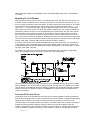
From the point of view of model creation, this process is handled in Proteus VSM by the
ISPICEMODEL::trunc function, which offers each model the chance to accept or reject a proposed
value for the next time step. Fortunately, SPICE does the rest.
HOW DSIM WORKS
Introduction
Digital transient analysis is perfomed using a technique known as Event Driven Simulation. This is
different from the analogue transient analysis used by SPICE in that processing only occurs when
some element of the circuit changes state. In addition, only discrete logic levels are considered and
this enables component functionality to be represented at a far higher level. For example, we can
think of a counter in terms of a register value that increments by one each time it is clocked, rather
than in terms of several hundred transistors. These make event driven simulation several orders of
magnitude faster than analogue simulation of the same circuit.
The Boot Pass
The purpose of the boot pass is to define the initial states of all nets in the circuit, and to given
every model at least one call to its simulate function.
The boot pass is carried out as follows:
•
All input pins connected to the VCC and/or VDD nets are deemed to be high.
•
All input pins connected to the GND and/or VSS nets are deemed to be low.
•
All input pins connected to a net to which a generator is connected are to deemed to be at the
same state as the INIT property of the generator.
•
All remaining pins are deemed to be initially floating.
• All models are requested (in no set order) to evaluate their inputs and set their output pins
accordingly.
• As nets change state, models connected to them are asked to re-evaluate their outputs. This
process continues until a steady state is found.
Settling Passes
Consider a chain of three inverters:
U1:A
1
U1:B
2
74LS04
3
U1:C
4
74LS04
5
6
74LS04
At the boot pass, each inverter except U1:A will see an undefined input state, and post an
undefined output state. However, U1:A's output will change state from from undefined to high and
because of this, a settling pass is run. U1:B is asked to re-simulate. This time it sees a logic 1 and
posts a logic 0 to its output. This changes the state of another net so another settling pass is run.
Eventually we get to a stage where U1:C has set its output high and no further changes have
occurred. At this point, the circuit is said to have settled.
Note that settling is deemed to take place before the simulation starts, and any time delays within
the models are ignored.
In a mixed mode simulation, settling passes can also occur whilst SPICE is trying to find the DC
operating point of the circuit.
The Event Processing Loop
Following the settling pass, DSIM begins the simulation process proper. The simulation is carried
out in a loop which passes repeatedly through the following two steps:
•
All the state change events for the current time are read off a queue and applied to the relevant
nets. This process results in a new set of net states.
•
Where a net changes state, all the models with input pins attached to the net are re-simulated.
Where their outputs change state, this creates new events which are placed on the event queue.
Of course, different models will create events which fall due for processing at different times. The
DSIM kernel thus has to order all the new events created at the end of each cycle round the loop.
It is also worth pointing out that our scheme quite happily supports models which have a zero time
delay. In this context, events generated with the same time-code are processed in batches (one
batch equals one trip round the loop), according to how they were generated.
Termination Conditions
Simulation stops when one of the following occurs:
•
The specified stop time is reached.
•
A logic paradox with zero time delay occurs such that the current time ceases to advance,
despite repeated cycles round the event processing loop.
• A system error such as running out of event queue memory arises. This is unlikely to occur in
normal use unless there is something unstable about your design, perhaps leading to a high
frequency (e.g. 100MHz) oscillation somewhere.
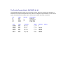
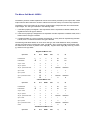
The Nine State Model
You might think that a digital simulator would model just logic highs and lows but in fact, DSIM
models a total of nine distinct states:
State Type
Power High
Strong High
Weak High
Floating
Undefined
Contention
Weak Low
Strong Low
Power Low
Keyword
PHI
SHI
WHI
FLT
WUD
CON
WLO
SLO
PLO
Description
Logic 1 power rail.
Logic 1 active output.
Logic 1 passive output.
Floating output - high-impedance.
Mid voltage from analogue source.
Mid voltage from digital conflict.
Logic 0 passive output.
Logic 0 active output.
Logic 0 power rail.
Essentially, a given state contains information about its polarity - high, low or mid-way -and its
strength. Strength is a measure of the amount of current the output can source or sink and
becomes relevant if two or more outputs are connected to the same net.
For example, if an open-collector output is wired through a resistor to VCC, then when the output is
pulling low, both a Weak High and a Strong Low are applied to the net. The Strong Low wins, and
the net goes low. On the other hand, if two tristate outputs both go active onto a net, and drive in
opposite directions, neither output wins and the result is a Contention state.
This scheme permits DSIM to simulate circuits with open-collector or open-emitter outputs and pull
up resistors, and also circuits in which tristate outputs oppose each other through resistors - a kind
of poor man's multiplexer if you like. However, it is important to remember that DSIM is a digital
simulator only and cannot model behaviour which becomes decidedly analogue. For example,
connecting overly large resistors up to TTL inputs would work OK in DSIM but would fail in practice
due to insufficient current being drawn from the inputs.
The Undefined State
Where an input to a digital model is undefined, this is propagated through the model according to
what might be described as common sense rules. For example, if an AND gate has an input low,
then the output will be low, but if all but one input is high, and that input is undefined then the
output will be undefined.
Floating Input Behaviour
It is common, if not altogether sound practice to rely on the fact that unconnected TTL inputs
behave as though connected to a logic 1. This situation can arise both as result of omitted wiring,
and also if an input is connected to an inactive tristate output. DSIM has to do something in these
situations since the internal models assume true logical behaviour with inputs expected to be either
high or low.
Should you wish DSIM to treated unconnected inputs in this way, you can assign the FLOAT
simulator control property to TRUE or FALSE. If this property is not specified, the default behaviour
is that unconnected inputs take the undefined state.
Glitch Handling
In designing DSIM we debated at great length how it should handle the simulation of models
subjected to very short pulses. The fundamental problem is that, under these conditions, a major
assumption of the DSIM paradigm - that the models behave purely digitally - starts to break down.
For example, a real 7400 subjected to a 5ns input pulse will generate some sort of pulse on its
output, but not one that meets the logic level specifications for TTL. Whether such an output pulse
would clock a following counter is then a matter dependent on very much analogue phenomena.
The best one can do is to consider the extremes, namely:
•
A 1ns input pulse will not propagate at all.
•
A 20ns pulse will come through nicely.
Somewhere in between, the gate will cease to propagate pulses properly and could be said to
suppress glitches. This gives us the concept of a Glitch Threshold Time, which can be an
additional property of the model along with the usual TDLH and TDHL.
Another subtlety concerns whether the glitch is suppressed at the input or the output of a model.
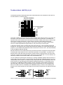
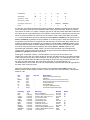
To resolve this, consider a 4-16 decoder driven from a ripple counter as shown overleaf.
The outputs of the ripple counter are staggered, and thus the possibility arises of the decoder
generating spurious pulses as the inputs pass through intermediate states. This situation is shown
in the following graph:
The above graph was produced with TGQ=0 for the 74154
Taking the first glitch an example of the phenomenon, as U1(QA) falls for the first time, it beats the
rise of U1(QB) and an intermediate input state of 0 is passed to the decoder for approximately
10ns. The question is whether the decoder can actually respond to this or not, and even more to
the point, what would happen if the input stagger was only 1ns or 1ps? Clearly, in the last two
cases the real device would not respond, and this tells us that we must handle glitches on the
outputs rather than the inputs. This is because, in the above example, the input pulses are all
relatively long and would not be considered glitches by any sensible criteria. Certain rival products
make a terrible mess of this, and will predict a response even in the 1ps case!
The really interesting part of this tale is that, if you build the above circuit, it will probably not glitch.
It is very bad design certainly, but the TDLH and TDHL of the '154 are around 22ns and this makes
it a tall order for it to respond to a 10ns input condition. With the individual components we tried,
no output pulses, other than perhaps the slightest twitches off the supply rails, were measurable.
To provide control over glitch handling, all the DSIM primitives offer user definable Glitch Threshold
Time properties named TGxx, where xx is the name of the relevant output. Our TTL models are
defined such that these properties can be overridden on the TTL components, and the values are
then defaulted such that the Glitch Threshold Times are the average of the main low-high and
high-low propagation delays. Setting the Glitch Threshold Times to zero will allow all glitches
through, should you prefer this behaviour. The graph, above, was thus created by attaching the
property assignment TGQ=0 to the 74154.
Finally, it is important to point out that if the Glitch Threshold Time is greater than either of the
low-high or high-low propagation delays, then the Glitch Threshold Time will be ignored. This is
because, after an input edge, and once the relevant time delay has elapsed, the gate output must
change its output - it cannot look into the future and see whether another input event (that might
cancel the output) is coming. Consider a symmetric gate with a propagation delay of 10ns and a
Glitch Threshold Time of 20ns. At t=0ns the input goes high and t=15ns the input goes low. You
might expect this to propagate, with the output going high at t=10ns and low again at t=25ns, so
producing a pulse of width 15ns which would be suppressed, since it is less than the Glitch
Threshold Time. The reason the pulse is not suppressed is that, at t=10ns, the output must go
high - it cannot remain low for a further 20ns on the off chance (as in our example) a second edge
comes along so producing an output pulse it would need to suppress! Once the output has gone
high at t=10ns then the second edge (at t=25ns) is free to reset it. You will need to think carefully
about this to understand it.
HOW MIXED MODE SIMULATION
WORKS
Overview
In the first instance, any circuit can be treated as being analogue, with the behaviour of digital
components such as a NAND gate being modelled by drawing their internal circuit - a complement
of 8 transistors for a single TTL NAND gate. This approach gives extremely accurate results, and
will tell you exactly what a 7400 gate will do if you put 1.8 volts on one input and 4.3V on the other.
However, given that it takes 9 gates to make a J-K flip flop and 4 such flip flops to make a 4 bit
counter, you will see that using this approach to model digital circuits of significant size becomes
excruciatingly slow.
Instead, digital circuits are normally simulated using an event driven approach. In other words, the
simulator only does work when some part of the circuit changes state. This is quite different from a
SPICE type simulator which repeatedly solves the entire circuit at fairly regular time intervals. In
addition, an event driven digital simulator is only interested in three logic levels - high, low or
undefined, and it does not worry about the exact way in which the real waveforms rise and fall.
These two factors mean that a digital simulation of a given circuit will be several orders of
magnitude faster than an analogue simulation of the same circuit, but at the expense of some
approximation of the true behaviour of the circuit. In particular, behaviour related to non-standard
voltages at logic inputs and very short input pulses cannot be modelled precisely.
The greatest difficulty arises when a circuit contains significant sections of both analogue and
digital circuitry, and it is the ability of a program to use both types of simulation simultaneously that
defines it as a Mixed Mode simulator. There a number of ways in which this can be achieved; in our
version we have aimed to get maximum efficiency for the digital simulation, at the expense of some
accuracy if digital parts are used in a seriously analogue way. For example, we have not attempted
to model the fact that a 4000 series buffer will make quite a nice amplifier if operated at around half
supply. Our view is that if you are interested in this kind of behaviour, you should be using a wholly
analogue model, drawn with the appropriate MOSFETs from the SPICE library.
In summary, PROSPICE mixed mode simulation works as follows:
•
Each net of the circuit is analysed to see whether analogue, digital or both types of component
are connected to it.
•
Where analogue components drive digital inputs, analogue to digital converter objects are
inserted and vice versa.
•
The SPICE simulation then proceeds as usual except that the ADC objects monitor their input
levels and create digital events when they deem that a change of state has occurred. Such
transitions cause a digital simulation pass to occur which may create events that affect the DAC
outputs at a future time. Analogue simulation then continues with DAC objects varying their
outputs according to the events that have been posted to them, rather in the manner of analogue
voltage generators.
There is somewhat more to it than this, because of the possibility of digital events being created
asynchronously (e.g. by a digital clock generator) and the need to prevent the analogue simulator
running past these timepoints, but that aside you have the essence of it.
The key point is that large amounts of activity can occur within the digital sections without the
overheads of analogue simulation, unless they actually change the voltages on analogue nets. You
could have an entire microprocessor model present which would involve thousands of digital events
being processed between any action on the analogue side of the circuit.
Mixed Mode Interface Models (ITFMOD)
In designing our scheme for mixed mode simulation within PROSPICE, we gave considerable
thought to the problem of how to specify the analogue characteristics of a device family. These
characteristics include:
•
The input and output impedances of the devices.
•
The logic thresholds of device inputs.
•
The voltage levels for high and low outputs.
•
The rise and fall times of device outputs.
A scheme which involved specifying all these parameters for every device in the TTL libraries, say,
would be extremely unwieldy.
In addition, a significant problem arises (for beginners, at least) in the specification of power
supplies - there is a tendency to plonk down a circuit such as the one below and expect sensible
results. The problem here, of course, is an implicit assumption that the 7400 has a 5V power rail
obtained from its hidden power pins which connect to VCC/GND.
All these problems are solved by the introduction of the ITFMOD component property. This is very
similar to the MODEL property in that it provides a reference to a set of property values but it also
activates a special mechanism within the netlist compiler. Essentially this works as follows:
•
For any device that has an ITFMOD property an additional model definition is called up during
netlisting that will specify control parameters for ADC and DAC objects, and also the pin names
of the positive and negative power supplies. In the above circuit, U1:A will have ITFMOD=TTL.
•
Having obtained the names of the power supply pins (VCC, GND in this case), ISIS creates a
special primitive and connects it across the power supply pins. ISIS names this object similarly
to an object on the child sheet or model, so that in the above circuit, the power supply object will
be called U1:A_#P.
•
When PROSPICE simulates a mixed mode circuit, it creates ADC and DAC objects and
considers them to ‘belong’ to the objects to which they connect. In the case of the circuit above,
a DAC object will be created with the name U1:A_DAC#0000 because it forms the interface from
U1:A’s output.
The clever part is that on doing this, it also looks for a power supply interface object with the
same name stem i.e. U1:A, and finds U1:A_#P. It then instructs U1:A_DAC#0000 to take its
properties from U1:A_#P which in turn has inherited its properties from the model specified in the
original ITFMOD assignment. Thus the DAC object operates with parameters defined for the TTL
logic family.
•
Each power interface object also contains a battery which will be assigned the VOLTAGE
property given in the interface model definition. The TTL interface model definition specifies
VOLTAGE=5V.
This means that in the above circuit, a 5V battery gets inserted between VCC and GND, because
these are the nets indicated by the power pins of the 7400 device.
•
The batteries have an internal impedance which can be assigned by the RINT property. It
defaults to 1miliohm. This means that if you assign a real power rail to VCC/VDD (by placing a
power terminal or voltage source) then this will override the level defined by the internal batteries in the world of simulation, a large current flow through the batteries does not matter!
The internal battery of an interface model can be disabled by assigning RINT=0.
Using ITFMOD Properties
Existing interface models have been defined as follows:
TTL
TTLLS
TTLS
TTLHC
TTLHCT
CMOS
MMOS
PLD
Standard TTL (74 series)
Low power Schottky TTL (74LS series)
Standard Schottky TTL(74S series)
High Speed CMOS TTL (74HC series)
High Speed CMOS TTL with TTL outputs (74HCT series)
4000 series CMOS.
Microprocessor type MOS circuits.
PLD type MOS circuits.
It follows that any new digital model can be assigned a device family by adding a property such as
ITFMOD=TTL
The family definitions are held in the file ITFMOD.MDF which is kept in the models directory.
Each definition can contain any or all of the properties defined for the ADC and DAC interface
primitives. In addition, the following may be given:
V+
VVOLTAGE
RINT
5V
1mΩ
Name of the positive power supply pin.
Name of negative power supply pin.
Specifies the default operating voltage.
Specifies the impedance of the internal battery. A value of
zero will disable the battery.
Finally, it is worth pointing out that any specific property e.g. TRISE, can be overridden on the
parent device, so if you want simulate a 4000 series IC with a slow rise time, you could add
TRISE=10u directly to its property list.
TYPES OF MODEL
Overview
There are essentially two types of model within Proteus VSM - electrical models and graphical
models. Within these two main categories there further sub-divisions.
Electrical Models
This type of model is that which is traditionally associated with circuit simulation. Most commonly,
an electrical model for a component will be created by drawing a circuit that mimics the behaviour
of the real device. We call this a Schematic Model. The components used in the model circuit are
drawn from a library of primitives which are built into the simulator itself. These primitives include
not only basic components such as resistors, capacitors, diodes and transistors, but also a
number of idealized devices such as voltage controlled current sources, ideal amplifiers and so
forth. Proteus VSM offers a large number of primitive devices - both analogue and digital - and
detailed information about them is included within this documentation.
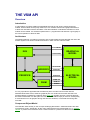
It is also possible to created electrical models programmatically using the VSM API. Interfaces are
provided for both analogue (SPICE) and digital (DSIM) models. Mixed mode components can be
modelled by implementing both interfaces within the same model DLL. In addition, an electrical
model implemented using the API can interact directly with an associated graphical model and this
leads to all kinds of exciting possibilities.
A third class of electrical models is that based around the standard SPICE Netlist format. This has
become a de facto standard for the description of analogue device models and many component
manufacturers now provide SPICE models for their wares on their web sites. Information on how to
make use of these models is contained within the main Proteus VSM User Manual.
Graphical Models
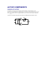
Proteus VSM is unique in providing a means for modelling components with which you can interact
whilst the simulation is running. Obvious examples include 7 segment LED displays and switches,
but much more complex components such as alphanumeric LCD displays can also be modelled
given the necessary development effort. The simpler devices can be modelled without recourse to
programming. A scheme is provided which displays one of a given number of graphical 'sprites'
according to a measured node voltage or logic state. We call these devices Active Components.
However, to unleash the real power of the system requires use of the VSM API. This provides a set
of interfaces through which a model can do almost anything that is possible in Windows itself. It
can draw directly onto the schematic, or into a popup-window of its own, or do both at the same
time. More often than not, a complex graphical model will be combined with an electrical model
within the same DLL - the alphanumeric LCD display model is an excellent example of how this
approach can bear fruit.
TYPES OF MODEL
Simulator Primitives
These are devices which are built into PROSPICE, either as part of SPICE3F5 for analogue
components or DSIM for digital components. Simulator primitives can be used to directly model
some components (e.g. resistors, capacitors, diodes, transistors) or as the building blocks for
modelling more complex devices - i.e. as part of a schematic model.
A simulator primitive is identified to the simulator by the PRIMITIVE property. For example, an
NPN transistor would be assigned:
PRIMITIVE=ANALOG,NPN
This tells the system that the transistor will be modelled by SPICE, and that the NPN primitive type
should be used.
Similarly, a two input NAND gate primitive would carry:
PRIMITIVE=DIGITAL,AND_2
ISIS library parts for the available primitives may be found in the ASIMMDLS and DSIMMDLS
libraries. There are also some special primitives used for making active components in
REALTIME.LIB.
Most of the primitive models have a number of properties which can be edited through the Edit
Component dialogue form. The models are also linked to the help topics within this document.
TYPES OF MODEL
Schematic Models
The most common method of modelling more complex devices such as op-amps and the larger TTL
and CMOS devices is through the use of schematic models. A schematic model is a circuit
constructed entirely out of simulator primitives that has the equivalent electrical behaviour to the
part being modelled. Note that it does not have to be (and usually is not) the actual internal
schematic of the IC.
For the purposes of testing, a schematic model is usually created as a child sheet of the part being
modelling. This allows a test circuit to be drawn on the parent sheet - we refer to this arrangement
as a Test Jig. Once the model has been proven, it can be compiled to an MDF (Model Description
Format) file using the Model Compiler command.
To attach an ISIS library part to an MDF file, the MODFILE property is used. For example, the 741
in OPAMP.LIB carries the assignment:
MODFILE=OA_BIP
When a 741 is encountered in a circuit, ISIS replaces it with the circuit described by OA_BIP.MDF.
Rather more cleverly, this particular model is parameterized. The VALUE property of the parent part
(741 in this case) is used to select particular property values for certain primitives in the model. This
is achieved through the use of the a MAP ON script block within the model and allows one model
file to be used for a number of different op-amps. Further information may be found under
Parameterized Circuits within the ISIS documentation.
Detailed instructions on how to go about creating new schematic models are provided in the
Analogue and Digital modelling tutorials.
TYPES OF MODEL
SPICE Models
The original Berkeley SPICE netlist format has established itself as a de-facto standard analogue
device models. A large number of component manufacturers now make available SPICE models for
their wares and PROSPICE is supplied with several thousand of these models. It is also relatively
straightforward to attached any such models you may obtain yourself to suitable ISIS library parts;
instructions for doing this are provided within the main PROSPICE documentation under USING
SPICE MODELS.
Since these models are simulated by the SPICE Kernel itself, they are presented to the rest of the
system as primitives. Typically they will carry property assignments such as
PRIMITIVE=ANALOG,SUBCKT
SPICEMODEL=LM741/NS
SPICELIB=NATOA
The SPICEMODEL property specifies the name of the SPICE model to use whilst the SPICELIB
property indicates the SML (SPICE Model Library) file that contains it. If the SPICE model was
located in an ordinary ASCII SPICE file, you would use the SPICEFILE property instead.
TYPES OF MODEL
VSM Models
VSM Models are much the same as simulator primitives except that they are held in DLLs rather
than within the PROSPICE simulator executables. The use of DLL based models provides an
alternative approach to schematic modelling when it comes to the simulation of very complex
components such as microprocessors. Uniquely in Proteus VSM, these models can also
implement graphical functionality which facilities the simulation of not only the electrical behaviour
of a device, but also its user interface. The possibilities that this unleashes are pretty much mind
boggling.
A very large part of this document is devoted to documenting the VSM API - that is the C++
programming interfaces through which ISIS and PROSPICE communicate with VSM models. In
addition, an example of a simple model is given to get you started.
Typically, a VSM model will carry property assignments such as:
PRIMITIVE=DIGITAL,8052
MODDLL=8051.DLL
The PRIMITIVE property indicates that the component is simulated directly by PROSPICE (so
that ISIS does not replace it with the contents of an MDF file), whilst the MODDLL property specifies
the name of the DLL that contains the 8052 model. Note that the second argument of the
PRIMITIVE property (8052 in this case) is passed to the DLL, enabling one DLL to contain models
for a number of different devices.
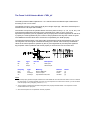
ANALOGUE MODELLING TUTORIAL
Introduction
In this tutorial we are going to model a relay consisting of two elements: a relay coil and a
single-pole, double-throw (SPDT) switch. These device elements already exist in the ISIS DEVICE
library as RELAY:A (the coil element) and RELAY:B (the switch element), and are shown below:
The relay is very simple in operation. When the voltage across the coil is lower than Von the relay is
'off' and the common pole of the switch (pin 3) is connected to the normally connected (NC) contact
(pin 4). When the voltage across the coil rises above Von the relay switches 'on' and the common
pole of the switch (pin 3) is connected to the normally open (NO) contact (pin 5). The relay remains
on until the voltage across the coil drops below Voff at which point the relay switches 'off' and the
common pole of the switch (pin 3) returns to connect to the normally connected (NC) contact (pin
4). Thus, the relay exhibits hysteresis - the 'on' voltage level is higher than the 'off' voltage level.
We shall model each element with its own equivalent circuit - that is a circuit that implements the
same functional and temporal behaviour as the element itself. You can find the complete design for
this tutorial in the Samples\Tutorials subdirectory under as AMODTUT.DSN.
Setting Up A Test Jig
The first thing we must do before we actually start to model the relay is to set up a test jig, as
shown below:
The test jig consists of an instance of the relay's coil element (RELAY:A picked from the DEVICE
library) and an instance of relay's switch element (RELAY:B, picked from the same library). The coil
has been wired so as to be driven by a Pwlin generator, whilst the switch element has been wired to
connect a 10V battery across one of two load resistors. In order to observe the switching action of
the relay, two voltage probes have been placed on its outputs and these together with the Pwlin
generator have been added to an Analogue graph. Note that the Pwlin generator's V(n) properties
have been assigned a set of values that produce a simple ramp-up/sustain/ramp-down signal; these
values have been chosen fairly arbitrarily and can be modified latter if this pulse is not suitable to
our needs.
Modelling The Coil Element
Having drawn the test jig, we now move on to modelling the relay's coil. Before we can do this, we
must first create a sub-sheet for the coil element on which we can place the equivalent circuit. To
do this, tag the coil with the right mouse button, and then click the left mouse button on it to edit it.
On the Edit Component dialogue form, edit the name of the component element to be RL1:A, its
value to be COIL and check the Attach Hierarchy Module check-box and click on the OK button;
ISIS creates a sub-sheet for the coil. When the design is netlisted, the coil component element is
replaced by whatever circuitry is on the sub-sheet and any connections to the pins of the coil will
be continued to any like-named terminals on the sub-sheet. The new sheet will have the name
RL1:A from the coil's reference and is thus unique to this coil instance (there should never be two
RL1:A component elements in the design). Similarly the circuit on the sub-sheet will have the name
COIL from the coil component element's value and is thus common to all components in the design
with the value "COIL" and their Attach Hierarchy Module checkbox checked.
To see the sheet (and thus the circuit) associated with a particular component, you must zoom in
to it by pointing at the component with the mouse and pressing CTRL+'Z' (Zoom-in). Do this now.
The Editing Window and Overview Window are redrawn and should show an empty sheet. To zoom
out again, press CTRL+'X' (eXit).
So to begin our model, zoom in to the coil's sheet as described above and enter the equivalent
circuit. The complete circuit we are going to use for the coil is shown below:
All the devices are PROSPICE primitives picked from the ASIMMDLS library via the Device Library
Selector dialogue form; the Pick Device/Symbol command on the Edit menu should not be used in
case devices from the DEVICE library are picked by mistake. The Default terminals are accessed
with the Terminals icon selected. Finally, the DEFINE and comment scripts are placed with the
Script icon selected.
Overview Of The Coil Circuit
The purpose of the coil's equivalent circuit is take the coil voltage (applied across the terminals C1
and C2) and according to the Von and Voff parameters, produce a positive or negative output gating
signal (across the GATE+ and GATE- terminals) according to whether the coil is 'on' or 'off'.
The input stage of the model consists of an inductor (L1) and a resistor (R1) in series. The inductor
models the coil's inductance whilst the resistor models the coil's bulk resistance. Both the
inductor's and resistor's value has been specified as mapped values. A mapped value is simply the
name of a property, enclosed in opening ('<') and closing ('>') chevrons. For example, the value:
<BETA>*2
indicates that the value of the component is to be assigned the mapped value <BETA> multiplied
by two. When ISIS links the model's netlist (the MDF file) to the design netlist prior to a simulation
run, it replaces the mapped value (that is, the chevrons and the property name enclosed between
them) with the value of the named property. This substitution is literal, so for example, if the
property BETA has been assigned as follows:
BETA=10+20
then a component value of <BETA>*2 will be replaced with:
10+20*2
The string of characters "<BETA>" has been replaced with the string of characters "10+20" since
ISIS does not attempt to interpret the value assigned to the mapped property. Although the value
has been assigned an expression, the assignment still works because all value and property
assignments are assumed to be expressions by PROSPICE and are automatically evaluated before
use. However, because the expression evaluator used by PROSPICE has a higher precedence for a
multiply operator than an addition operator, PROSPICE will evaluate this expression as 10+(20*2) =
50 - not what was expected! If you are worried that such mistakes may occur, then you should
declare the component value as:
(<BETA>)*2
This will expand (after parameter mapping) to (10+20)*2 which will then evaluate correctly to 30*2 =
60.
Properties for mapped values can be assigned in one of two ways: as a property within the parent
component or on the equivalent circuit's sheet, via either a DEFINE or MAP ON script. If a property
is assigned in both places, then the value assigned in the parent component has the highest
precedence. This precedence is vital in order to allow default values to be overridden by the user.
Thus, in our model, we have specified a default inductance and series resistance of 100mH and 100
Ω respectively via the DEFINE script. However, the user of the model can specify alternative
value(s) by adding an assignment to the parent component's Properties list.
The output stage of the model consists of a voltage-controlled switch, VSW2, two batteries (GB1
and GB2) and a series resistor, R4. When the switch is off, the output voltage is -2V, set by GB2
and R4; when the switch is on, the output voltage is +2V, set by GB1 (R4 serves to make GB2
open-circuit for low currents).
Unfortunately for us, whilst the output resistance of PROSPICE's VSWITCH model is Ron at or
above Von and Roff at or below Voff , it is also linear between these control voltages. Thus we
cannot use VSW2 to directly model hysteresis but must do this ourselves. This is the purpose of
the resistor divider formed by R2 in parallel with VSW1 and R3. The values of R1 and R2 are set to
(nominally) divide by ten and also so as not to unduly load the inductor and series resistor. For the
latter reason, R2 and R3 are both parameterized in terms of the value of R1.
The switches' 'on' voltages (specified by the VON property) have been set to 0.1<VON>, since this
is the nominal output voltage produced by the divider when the voltage applied to the coil is <VON>.
In order that the switches switch cleanly between their 'on' and 'off' states, the 'off' voltages
(specified by the VOFF property) are also set to be the same.
We must now determine the on-resistance for the VSW1 such that, once the coil is 'on' (VSW1 and
VSW2 both on), the resistance of the upper part of the divider is such that, given an voltage applied
to the coil of <VOFF>, the output of the divider is 0.1<VON> (the switches' off voltages as set by
VOFF property). This is better explained by way of the diagram below:
R2
9<RC>
VSW1
Ron
<VOFF>
R3
<RC>
0.1<VON>
Using Ohm's law (or the voltage divider rule), the diagram yields:
R3
0.1 < VON >=< VOFF >
( R2Ron ) + R 3
Where <VON> and <VOFF> are mapped parameters (the on and off coil voltages the relay
switches at), R2 and R3 are 9*<RC> and <RC> respectively (<RC> is the mapped coil resistance,
as specified in the value of R1), and Ron is the unknown value we require for VSW1. If you do the
algebra, Ron comes out to be:
< VOFF
9 < RC > < VON > −
10
Ron =
< VOFF > − < VOFF >
>
which (in expression form) is what is assigned to the RON of VSW1.
The equivalent circuit connects to its parent component's pins through terminals with the net names
the same as the parent component's pins - C1 and C2. As the parent pins are passive, we have
used Default terminals; for other types of pin you would use the corresponding terminal type. When
netlisting a design, if ISIS finds any parent component pins not represented on the sub-sheet by
terminals it issues a warning (in case we have forgotten to connect them or in case we have
connected them but mistyped the terminal name). Note that ISIS only checks that there is at least
one like-named terminal for each of the parent component's pins - it will not report the existence of
additional terminals with names that do not match parent component pins. In particular, where you
are referencing a parent pin several times through more than one terminal, be aware that typing
errors in one or more terminals' names will not be detected or reported.
Very often, you may find yourself modelling a component or component element you didn't create
yourself and whose pin names are not visible (in our case, the relay coil). The question then arises
as to how you find out the component's pin names? The quick answer is to move the mouse over
the pin ends - information about the pin including its name, number and electrical type will be
displayed on the status bar.
In order to connect to the equivalent circuit of the relay's switch, we have again used Default
terminals, but this time, we have given the terminals a net name beginning with an asterisk
character ('*'). When ISIS creates the simulation netlist, all like-named nets preceded by an
asterisk on different child sheets of the same parent part (in our case RL1) are deemed connected
and are merged to form a single net. This facility is provided specifically for making connections
across different child sheets in modelling multi-element (heterogeneous or homogeneous) devices.
Modelling The Switch Element
Having modelled the coil, the switch's equivalent circuit is relatively straight forward, and is shown
below:
As with the relay coil, before we can enter the equivalent circuit for the switch, we must first edit the
RELAY:B component element instance, set the component's reference to RL1:B, its value to
SWITCH, and check its Attach Hierarchy Module checkbox to create the sub-sheet for the
equivalent circuit.
To enter the equivalent circuit, we then need to zoom in to the switch's sub-sheet by pointing at the
switch and pressing CTRL+'Z'. The equivalent circuit can then be entered as usual. The circuit itself
consists of two voltage-controlled switches (VSW3 and VSW4), two capacitors (C1 and C2) and
four diodes (D1 through D4). All the devices used are picked from the ASIMMDLS library via the
Device Library Selector dialogue form; again the Pick Device/Symbol command on the Edit menu
should not be used in case devices from DEVICE are picked by mistake. The Default terminals are
accessed with the Terminals icon selected. Finally, the DEFINE script is placed with the Script
icon selected. The script can be edited either within ISIS or using an external text editor - see
Placing & Editing Scripts in the ISIS manual.
Overview Of The Switch Circuit
The switch's control pins are wired with opposite polarity such that only one switch is on at a given
moment. Both the switches have the same Von and Voff control voltages (specified by the VON and
VOFF properties) and these are set to be 1V - the middle of the control voltage generated by the
coil model. Thus each switch changes state simultaneously. The off-resistances of both switches,
set by the ROFF property are set to the constant 1TΩ; the on-resistances, set by the RON
property, are set to the mapped property RON, which is defaulted to 10mΩ via a DEFINE script.
Each switch contact has an output capacitance modelled by a single 10pF capacitor between the
output and the common pole of the switch as well as two back-to-back passive diodes.
The latter do not perform any function in the model but are useful ruse for tricking the PROSPICE
simulator engine in to making more calculations around sudden output transients (that are to be
expected considering the nature of the model). Without these diodes, you may well find the
VSWITCH model appears to switch slowly as PROSPICE will not consider the switching point in
detail. The alternative 'fix' to this problem is to assign the PROSPICE NUMSTEPS Simulation
Control Property a high value - this however results in PROSPICE running the entire simulation with
a small time step and therefore overall simulation time is lengthened.
As with the relay coil model, we have used Default terminals with names the same as the parent
component's pins to interconnect the model with the parent component and have used terminals
with names beginning with an asterisk character ('*') to interconnect the switch model with the coil
model (see the preceding section for a fuller explanation).
Testing And Compiling The Model
To test the model, we zoom out of the switch sub-sheet (using either the Exit To Parent command
on the Design menu or its keyboard short-cut, CTRL+X (eXit) and then simulate our test circuit, by
either invoking the Simulate command on the Graph menu or its keyboard shortcut - the
spacebar.
Not surprisingly, our equivalent circuit model works first time. The default hysteresis values of 5V (V
on) and 2V (V off ) are clearly seen to work. However, if the simulation results were not as expected,
we could zoom back in to either coil or switches sub-sheet, edit the equivalent circuit, zoom out,
and re-simulate it. This simulate-edit-simulate cycle could be repeated as many times as is
necessary to get the equivalent circuit working. Further, if the model didn't work and we were
unsure why, we could zoom in to the sub-sheet and add additional probes (say, on the output of the
coil model to see whether the correct polarity and voltage levels were being produced at the *GATE
terminals) and then add this probe to our graph by zooming out to the root sheet and using the Add
Trace command on the Graph menu. You can even Quick Add probe(s) on a sub-sheet by first
tagging them, then zooming out, and then invoking the Add Trace command and affirming the
Quick Add? prompt. Once the model works, you would then zoom in to the sub-sheet(s) and
remove the probes - they would not only be redundant in future use but would also slow down the
simulations using the model.
Having finished the relay model and tested it, we must now separately netlist the coil and switch
circuits to external model (MDF) files. To do this, we need to zoom in to the respective sub-sheet
and invoke the Model Compiler command from the Tools menu. The command causes a file
selector dialogue form to be displayed prompting for the name of the model file - the default is the
name of the design file, with an MDF extension, and the directory selected is that specified by the
Module Path field of the Set Paths command's (System menu) dialogue form. The Module Path
directory is the directory where ISIS looks to locate a model file specified by a component's
MODFILE property (ISIS first looks in the current working directory, but it is unlikely that you would
have model files there except possibly for testing). We will call our coil model RLY_COIL.MDF and
our switch model RLY_SW.MDF. For each sub-sheet, type the respective filename in to the
Filename field of the filename selector and select the OK button.
Using The Model In Future Designs
We have now created our model. In future designs, whenever we wish to model a relay coil
component element, all we need do is edit the element instance and add the following property
assignment to its list of properties:
MODFILE=RLY_COIL.MDF
We would probably also want to specify our own inductance, series resistance, and hysteresis
voltage levels, so we would also need one or more additional property assignments of the form:
LC=120m
RC=50
VON=8
VOFF=5
The MODFILE= assignment tells ISIS that, when creating the simulation netlist, the component
should be removed from the netlist and replaced with the netlist contained in the RLY_COIL.MDF
model file. This process is referred to as netlist linking since it involves ISIS in linking the netlist
contained in the model file to the design's simulation netlist. It involves three key stages:
1. All connections to the coil component are linked to the like-named nets in the model file's netlist.
2. All connections within the model file's netlist to nets whose names begins with an asterisk ('*')
character are connected to like-named nets in any other child sheets of the component. In our
case, because the relay is a multi-element heterogeneous device, the coil and switch elements
are both part of the same component (RL1).
3. All mapped property values in the model file's netlist are replaced as previously described. As
was stated, where a property is assigned both within the component instance (i.e. the
component using the model) and within the respective model file's netlist, the former has
precedence.
The same is true for modelling a relay switch element. The element needs to be edited and
assigned a MODFILE property, as follows:
MODFILE=RLY_SW.MDF
As with the coil, if you wanted to override any of the default parameters of the model, then you
would need additional property assignments. For example, to specify a different contact
on-resistance, you might add the following:
RON=50m
These sorts of assignments are fine for one-time modelling, but become tiresome in use. Further,
you very often forget what parameters a given model supports and what the exact property name for
the parameter is. Thus, our final action is to add the MODFILE and other property assignments to
the RELAY:A (the library name for the relay coil) and RELAY:B (the library name of the relay
switch) devices in the library. Then, whenever these devices are picked from the library and placed,
the new component element instances will be automatically annotated with the correct properties
already assigned.
To add the property assignments to the relay coil library part, zoom out to the root sheet, tag the
coil component element (RL1:A), and invoke the Make Device command on the Edit menu. Then
click the Edit Properties button. The main combo-box on this form lists all the default properties for
the device, including any assignments that have been made to the component on the schematic.
ISIS already knows about MODFILE because it is a standard property in LISA, but LC, RC, VON and
VOFF are specific to our relay coil and will be treated as strings unless other information is given.
For example, the settings for LC might be changed as follows:
The Description might be ‘Coil Inductance’
The Type should be Float to indicate that a floating point number is expected.
The Limits should be positive, non-zero since negative or zero values are not allowed for the
inductance.
Similar information can be entered for the other parameters – this has the major advantage that a
future user of the model can see exactly what needs to be entered, and what defaults are in use.
The same procedure is applicable to the relay switch element.
Finally, before quitting ISIS, always save your design to a back-up directory in case you lose your
model (MDF) files or in case you subsequently discover an error in your model.
DIGITAL MODELLING TUTORIAL
Introduction
In this tutorial, we are going to model (one half) of the 74123 TTL monostable multivibrator. For
those not familiar with the device, its behaviour has been summarized in the next see section.
We are, in fact, going to model three devices: the 74123 (standard TTL), the 74LS123 (low power
Shottky TTL) and the 74HC123 (high speed CMOS TTL). All the three devices have identical
functional behaviour - the only difference between them is in their transient behaviour - and so they
can all be modelled with a single equivalent circuit. An equivalent circuit is a circuit that uses only
digital primitive devices (from the DSIMMDLS library) wired so as to behave, functionally and
temporally, as the respective 74XX123 device. The name 74XX123 implies any of the three devices
and we will refer to our model via this generic name. We will model the different timing behaviours of
each device by specifying the equivalent circuit's timing properties as mapped values; ISIS will then
map the correct set of timing values at the time the model is used - the set of values being chosen
according to the Value field (or the VALUE component property) of the component using the model.
The complete design for this modelling tutorial can be found in the Samples\Tutorials sub-directory
as DMODTUT1.DSN.
The 74123 Monostable Multivibrator
The TTL 74123 consists of two independent monostable multivibrators. Each monostable has a
negative edge trigger (A), a positive edge trigger (B), an overriding clear (MR), two timing inputs (CX
and CX/RX) and both true and complementary outputs (Q and Q ). Given a suitable trigger condition
at one of the trigger inputs, the outputs produce a square-wave pulse whose duration is determined
by the resistor/capacitor network connected to the device's CX and CX/RX pins. As we will not be
using this network to determine the model's timing, we will not discuss these pins or their function
further.
The device and its truth-table are shown below.
Note that the monostable can be triggered by a rising edge at the MR input when the A and B
inputs are active. The 74123 is also a retriggerable monostable: once an output pulse has
commenced, the pulse can be extended by retriggering the device, as is shown below:
A
B
QA
QB
QAB
Pulse From
Negative Edge At A
Pulse From
Positive Edge At B
Actual Pulse At Q Output
The monostable is first triggered by a negative edge at the A input (with the MR and B inputs high).
Ordinarily, this would produce a pulse at the Q output as shown by the QA trace. However, the
monostable is then retriggered by a positive edge at the B input (with MR input high and A input
low). If an output pulse was not already in progress, this would produce a pulse at the Q output as
shown by the QB trace. Given that an output pulse is already in progress, the net result of the two
triggers is the overlap of the two output pulses, as shown by the QAB trace.
Setting Up A Test Jig
The first thing we must do before we actually start to model the monostable is to set up a test jig,
as shown below.
The test jig consists of an instance of the component we want to model (U1:A, a 74LS123
monostable), support circuitry necessary to test it (in our case, all we need is three Digital
generators and two voltage probes) and a Digital graph on which to display the results of the tests.
As shown in the screen shot, we have already annotated the generators and added both they and
the probes to the graph; as we have not done any tests as yet, the graph has no data. The
generator properties (INIT, WIDTH, etc.) have been chosen fairly arbitrarily - a set of pulses will be
generated on A and B whilst MR is held inactive, and then after 31µs, MR is taken active to test the
resetting of the outputs. Note that we haven't actually chosen values for the A and B probes that
guarantee an output pulse will be present when MR goes active - if this is not the case, we will see
it and can then simply 'tweak' the generator property values to generate an output pulse or reset at
the appropriate time.
Now that we have the test jig laid out, we can actually start to model our device.
Entering The Equivalent Circuit
The first thing we need to do is to is create a sub-sheet for the 74LS123 component on which we
can place the equivalent circuit. To do this, tag the 74LS123 with the right mouse button, and then
click the left mouse button on it to edit it. On the Edit Component dialogue form, edit the name of
the component to be U1:A, check the Attach Hierarchy Module check-box and click on the OK
button; ISIS creates a sub-sheet for the 74LS123. When the design is netlisted, the 74LS123 is
replaced by whatever circuitry is on the sub-sheet and any connections to the pins of the 74LS123
will be continued to any like-named terminals on the sub-sheet. The new sheet will have the name
U1:A from the 74LS123 reference and is thus unique to this 74LS123 instance (there should never
be two U1:A components in the design). Similarly the circuit on the sheet will have the name
74LS123 from the 74LS123 component's value and is thus common to all components in the design
with the value "74LS123" and their Attach Hierarchy Module checkbox checked - in theory this
should only be actual 74LS123 components.
To see the sheet (and thus the circuit) associated with a particular component, you must zoom in
to it by pointing at the component with the mouse and pressing CTRL+'Z' (Zoom-in). Do this now.
The Editing Window and Overview Window are redrawn and should show an empty sheet. To zoom
out again, press CTRL+'X' (eXit).
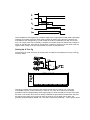
So to begin our model, zoom in to the 74LS123's sheet. The complete equivalent circuit we are
going to use to model our monostable with is shown below:
Entering the circuit is straight forward. The AND_3 and PULSE devices are both digital primitives
picked from the DSIMMDLS library, either via the Device Library Selector dialogue form or via the
Pick Device/Symbol command on the Edit menu. The Input and Output terminals are accessed
with the Terminals icon selected. Finally, the DEFINE and MAP ON scripts are placed with the Script
icon selected. These can be edited either within ISIS or using an external text editor - see Placing
& Editing Scripts in the ISIS manual.
Overview Of The Equivalent Circuit
The following sections give an explanation of how the equivalent circuit works - both functionally and
temporally - together with an explanation of some of the likely pit-falls of modelling digital devices
by an equivalent circuit.
Functional Modelling
The circuit consists of a AND_3 gate primitive that generates the trigger clock and a PULSE
primitive that takes care of generating the pulses and handling retriggering. Both these devices are
digital device primitives picked from the DSIMMDLS library.
The circuit connects to its parent component's pins through Input and Output terminals with the
same names as the parent component's pins - A, B, Q, etc. The complementary output (displayed
as Q ) is achieved by editing the terminal and assigning it the name $Q$ - see Making a Single
Element Device in the ISIS manual for an explanation of how dollar characters are used to achieve
an overbar. In our example, we know all the parent component's pin names, as they are all visible.
However, if we were modelling a component where this were not the case, we could easily find out
the details of a pin by tagging the parent component and then clicking left on the end of the pin we
are interested in. The component's Edit Component dialogue form is displayed in the usual way
except that, on the right hand side, are detailed the pin's name, number and electrical type (along
with the component's library name). After taking note, the form can be cancelled.
We have avoided using a separate inverter primitive to invert the A input and have instead used the
digital primitive INVERT property in the AND_3 primitive. The property assignment causes the
primitive model to invert the behaviour of the D0 input, so treating the input as active low. This
simplifies the circuit and leads to faster simulation runs.
There is no way for the equivalent circuit to determine the value or values of the components
connected to the parent component's RX/CX and CX inputs and thus there is no way these
components can be used to determine the output pulse width of the model. (Apart, of course, from
creating the model as a mixed mode model) Instead, we are going to force the user of the model to
specify a time constant value in the parent's property list.
When netlisting a design, if ISIS finds any parent component pins not represented on the sub-sheet
by terminals it issues a warning (in case we have forgotten to place them or in case we have placed
them but miss-typed their name). Note that ISIS only checks that there is at least one like-named
terminal for each of the parent component's pins - it will not report the existence of additional
terminals with names that do not connect with the parent’s pins.
In particular, where you are referencing a parent pin
several times through more than one terminal, be
aware that mistakes such as shown here (the name
CLR has been used when MR was intended) is not
reported. In order to avoid netlisting warnings with our
equivalent circuit, we have thus placed two terminals,
labeled them RX/CX and CX and connected them to
ground (leaving the terminals unconnected would have
worked equally well).
Our final action to complete the functional model is to edit the PULSE primitive and assign it the
property RETRIGGER=TRUE. By default the PULSE primitive ignores transitions at its CLK input
whilst an output pulse is in progress - however assigning the primitive's RETRIGGER property TRUE
causes the primitive to extend any on-going output pulses as a result of new transitions at the CLK
input.
Temporal Modelling
Having created the functional model, we now need to add some timing properties in order to
correctly model transient behaviour - we are not going to model set-up or hold times. The timing
parameters we are going to model are the time delays from clock (that is, a valid edge on A, B or
MR) to Q and Q outputs and the time delays from MR to Q and Q . The PULSE primitive supports
properties that directly model these delays so no further gadgets (such as DELAY primitives) are
required at the outputs.
The timing properties are assigned to the PULSE primitive by editing the component and entering
the required assignments in the Edit Component dialogue form's Properties text entry field. The
names of the properties we need to assign (e.g. TDCQ, TDCQB, etc.) are listed in the PULSE
primitive documentation. We could assign the properties literal (i.e. fixed) values - for example, if we
were modelling a 74LS123 (as opposed to the 74123 or 74HC123), we might enter the assignments:
TDCQ=22n
TDCQB=32n
TDRQ=20n
TDRQB=28n
This would work perfectly well for a 74LS123, however there are two drawbacks. The first drawback
is that the model cannot be used for a 74123 or a 74HC123 - the model would have the correct
functional behaviour, but not the correct timing behaviour. The second drawback is that there is no
way for a user of the model to override the default glitch timing values (specified with the TGQ and
TGQB properties) and initialization value (specified by the INIT property) on the parent component
(the component that uses the model). The solution to both these drawbacks is the use of mapped
values - instead of assigning the properties literal values, we assign them mapped values. A
mapped value is simply the name of another property, enclosed in opening ('<') and closing ('>')
chevrons. For example, the assignment:
TDCQ=<TD_CLK_TO_Q>*2
indicates that the property TDCQ is to be assigned the mapped value <TD_CLK_TO_Q> multiplied
by two. When ISIS links the model's netlist (the MDF file) to the design netlist prior to a simulation
run, it replaces the mapped value (that is, the chevrons and the property name enclosed between
them) with the value of the named property. This substitution is literal, so for example, if the
property TD_CLK_TO_Q has been assigned as follows:
TD_CLK_TO_Q=10n+20n
then the property assignment TDCQ=<TD_CLK_TO_Q>*2 will be replaced with:
TDCQ=10n+20n*2
The string of characters "<TD_CLK_TO_Q>" has been replaced with the string of characters
"10n+20n" - ISIS does not attempt to interpret the value assigned to the mapped property. Although
the TDCQ property has been assigned an expression, the assignment still works because all
property assignments are assumed to be expressions by DSIM and are automatically evaluated
before use. However, because the expression evaluator used by DSIM has a higher precedence for
a multiply operator than an addition operator, DSIM will evaluate this expression as 10n+(20n*2) =
50n - not what was expected! If you are worried that such mistakes may occur, then you should
declare the initial assignment as:
TDCQ=(<TD_CLK_TO_Q>)*2
This will expand (after parameter mapping) to (10n+20n)*2 which will then evaluate correctly to
30n*2 = 60n.
In general, if you are the originator and only user of the model, then these issues are not a problem.
However, if you feel that problems like these are likely to arise then model defensively.
Properties for mapped values can be assigned in one of two ways: as a property within the parent
component or on the equivalent circuit's sheet, either via DEFINE or MAP ON script. If a property is
assigned in both places, then the value assigned in the parent component has the highest
precedence. This precedence is vital in order to allow default values to be overridden by the user.
For example, we can define a default value for a mapped property via, say, a property assignment in
a DEFINE script on the equivalent circuit's sheet. The user can then override such an assignment
by specifying an alternative value via an assignment in the parent component's Properties list.
Thus, in our equivalent circuit, we have assigned all the PULSE primitive model properties mapped
values:
TDCQ=<TDCQ>
TDCQB=<TDCQB>
TDRQ=<TDRQ>
TDRQB=<TDRQB>
TGQ=<TGQ>
TGQB=<TGQB>
INIT=<INIT>
The mapped timing values are assigned via a MAP ON script:
*MAP ON
74123
74LS123
74HC123
VALUE
: TDCQ=19n, TDCQB=27n, TDRQ=18n, TDRQB=30n
: TDCQ=22n, TDCQB=32n, TDRQ=20n, TDRQB=28n
: TDCQ=29n, TDCQB=29n, TDRQ=31n, TDRQB=31n
The MAP ON script compares the value of the property named after the MAP ON keywords with each
of the strings to the left of the colons (the comparison is not case-sensitive). Given a match, all the
property assignments to the right of the colon and up to an end-of-line character are made. If you
have more property assignments that would easily fit on one line, use the line continuation
character ('\') to continue on to the next line:
*MAP ON VALUE
74123
: TDCQ=19n, TDCQB=27n, TDRQ=18n, \
TDRQB=30n
74LS123 : TDCQ=22n, ...
If none of the strings to the left of the colon match the value of the named property, then no property
assignments take place. The likely result of such a situation is that the netlist linker will report that
a mapped value cannot be mapped because the relevant property is not defined. Such behaviour
may be desirable where it is intended that the mapped value has to be (i.e. must be) assigned by
the user in the parent component using the model. If you want to add a default case to the MAP ON
block, you can do so by using the keyword DEFAULT to the left of the colon; if the value of the
named property is not matched with any of the other names to the left of the colons, then the
assignments to the right of the colon following the DEFAULT keyword will take place.
In our equivalent circuit, the MAP ON script reads: if the value of the VALUE property (defined by the
Value field of the parent component's Edit Component dialogue form or via an explicit assignment to
the VALUE property) is the string "74123", then assign the property TDCQ the value 19n, etc.; if the
value of the VALUE property is the string "74LS123" then assign the property TDCQ the value 22n,
etc.; and finally if the value of the VALUE property is the string "74HC123", then assign the property
TDCQ the value 29n, etc.
As we have already said, the pulse width of the 74XX123 monostable is determined by the
resistor/capacitor network around its RX/CX and CX pins and as we have no way of determining the
arrangement of the devices connected to these pins or their values we ignore them and force the
user to specify a time-constant value for the required width of the output pulses. Within the PULSE
primitive model, the output pulse width is specified by the WIDTH property and so we have assigned
this property the mapped value <TC> for Time-Constant. As all 74XX123 devices have a default
output pulse width of approximately 30ns when their CX/RX and CX inputs are unconnected, we
have specified this as the default value for the TC property via a DEFINE script. (alternatively, we
could have added the assignment to each set of assignments within the MAP ON script, but this
would have required additional typing).
By default, all timing parameters are subject to scaling by the Simulation Control Property TDSCALE
; if this property has been assigned the RANDOM keyword, then timing parameters are scaled by a
random value limited in range by the TDLOWER and TDUPPER Simulation Control Properties. Whilst
such behaviour is desirable for the primary timing properties (TDCQ, TDRQ, etc.), we might, as the
user of the model, quite reasonably expect that specifying TC=10u, say, would lead to output
pulses that are indeed 10µs wide. We have achieved this behaviour by use of the NOSCALE
property. This property is common to all DSIM primitives (which is why you won't find it listed under
the documentation for the PULSE primitive) and allows you to specify which properties are not to be
subject to the default scaling behaviour. Thus, we have added the line:
NOSCALE=WIDTH
to the PULSE primitive.
We have also assigned mapped values to the PULSE primitive's TGQ, TGQB, INIT properties. We
ourselves are not interested in these properties - we have only mapped them in order to allow the
user access to them. However, as we have already stated, if we don't provide default values for
these mapped values and the user doesn't, then the netlist linker will report an error when linking
the model's netlist to the design's netlist. So what default values should we assign? We could
assign INIT the value zero - Q initially low and QB initially high. This is not unreasonable and is in
fact the same as the model's default value for the property. TGQ and TGQB are somewhat more
complex, as the model's default values for these properties are based on the other timing
parameters (in fact, TGQ is half TDCQ and TGQB is half TDCQB). One solution would be to define
them within the MAP ON script with values applicable to the logic family concerned. The real solution
to our problems is in fact the question-mark ('?') value. We assign the INIT, TGQ and TGQB
properties values consisting of a leading question-mark (any spaces before and other characters
after the question-mark are ignored):
INIT=?
TGQ=?
TGQB=?
The question-mark informs DSIM to use the model's default value for the property. Thus, the netlist
linker replaces the mapped value <INIT> with the value of the INIT property - defined in the DEFINE
script as the string "?". DSIM sees the question-mark and ignores the attempted assignment and
instead uses the models default value - zero in the case of the INIT property, or half TDCQ(B) in
the case of the TGQ(B) property. Note that the model takes care of evaluating TDCQ first in order to
arrive at a default value for TGQ - there is no need to order the property assignments to achieve this.
Testing And Compiling The Model
To test the equivalent circuit, we zoom out of the sub-sheet (using either the Exit To Parent
command on the Design menu or its keyboard short-cut, CTRL+'X' (eXit) and then simulate our test
circuit, by either invoking the Simulate command on the Graph menu or its keyboard shortcut - the
spacebar.
Not surprisingly, our equivalent circuit model works first time. However, if the simulation results
were not as expected, we could zoom back in to the component's sub-sheet, edit the equivalent
circuit, zoom out, and re-simulate it. This simulate-edit-simulate cycle could be repeated as many
times as is necessary to get the equivalent circuit working. Further, if the model didn't work and we
were unsure why, we could zoom in to the sub-sheet and add additional probes (say, on the output
of the AND_3 gate to see whether the PULSE primitive was or wasn't being clocked) and then add
this probe to our graph by zooming out to the root sheet and using the Add Trace command on the
Graph menu. You can even Quick Add probe(s) on a sub-sheet by first tagging them, then zooming
out, and then invoking the Add Trace command and affirming the Quick Add? prompt. Once the
model works, you would then zoom in to the sub-sheet and remove the probes - they would not
only be redundant in future use but would also slow down simulations using the model.
If we wanted to test our model fully , we would need to not only test a 74LS123 but also the other
74XX123 devices modelled: the 74123 and 74HC123. Since these components have their timing
determined by the Value field of the parent component (via the MAP ON script), the easiest way to
test these devices would seem to be to edit the existing 74LS123 and change its Value field to
74123 or 74HC123. If you do this, you will find yourself with netlist compilation errors. Why? The
reason is that the equivalent circuit on the component's sub-sheet has a circuit name equivalent to
the Value field of the parent component - change the Value field and you change the circuit name.
The proof of this is that if you change the Value field to 74HC123 and zoom in to the sub-sheet you
will find it blank (because there is no 74HC123 circuit). Zoom out, change the Value field back to
74LS123, zoom back in, and Hey! Presto! the equivalent circuit reappears (unused circuits are kept
in the design - even saved to disk with it - until you use the Tidy command on the Edit menu to
remove them).
So how to we test the other models? The answer is to use a subtle ruse and overload the Value
field with a VALUE property. The name for a circuit on a component's sub-sheet is always taken
from the Value field. However, the VALUE property used in a netlist is taken first from any VALUE=
property assignment (in the Properties field of the Edit Component dialogue form) and then, if this
property is not defined, from the Value field. So to test say, the 74HC123, tag the component, click
left on it to edit it, and enter (in the Properties field) the assignment:
VALUE=74HC123
and select the OK button. You can now re-simulate the model as if the parent were a 74HC123.
Having finished the model and tested it, we must now netlist it to an external model (MDF) file. To
do this, we need to zoom in to the sub-sheet and invoke the Model Compiler command from the
Tools menu. The command causes a file selector dialogue form to be displayed prompting for the
name of the model file - the default is the name of the design file, with an MDF extension, and the
directory selected is that specified by the Module Path field of the Set Paths command's (ISIS
menu) dialogue form. The Module Path directory is the directory where ISIS looks to locate a model
file specified by a component's MODFILE property (ISIS first looks in the current working directory,
but it is unlikely that you would have model files there except possibly for testing). We will call our
model 74XX123.MDF. Type the name in to the Filename field and select the OK button.
Using The Model In Future Designs
We have now created our model. In future designs, whenever we wish to model a 74XX123 TTL
component, all we need do is edit the component and add the following property assignment to its
list of properties:
MODFILE=74XX123.MDF
We would probably also want to specify our own pulse width, so we would also need a second
property assignment of the form:
TC=500n
The MODFILE= assignment tells ISIS that, when creating the simulation netlist, the component
should be removed from the netlist and replaced with the netlist contained in the 74XX123.MDF
model file. This process is referred to as netlist linking since it involves ISIS in linking the netlist
contained in the model file to the design's simulation netlist. It involves two key stages:
1. All connections to the monostable component are linked to the like-named nets in the model
file's netlist.
2. All mapped property values in the model file's netlist are replaced as previously described. As
already stated, where a property is assigned both within the monostable component and within
the model file's netlist the former has precedence. Thus, with the TC property assignment given
above, the WIDTH=<TC> property assignment within the equivalent circuit expands to WIDTH
=200n (the suffix notation will be correctly interpreted by DSIM).
Our final action is to add the MODFILE and TC property assignments to the 123 device in the
respective library (the library device has the name 123, the 74, 74LS or 74HC prefix is only added
when the 123 device is picked from the library). Then whenever the 123 device is picked from the
library and placed, the new component instance will be automatically annotated with these
properties already assigned.
To add the property assignments to the library part, zoom out to the root sheet, tag the 74LS123
component, and invoke the Make Device command on the Edit menu. Then click the Edit
Properties button. In the combo-box you will see that the two properties MODFILE and TC have
appeared, because they were already assigned the component. Click first on MODFILE. ISIS
already knows about this property because it is a standard property name in LISA. You will see
that it is declared as read-only, and is normally hidden. Now click on TC this is a new property, and
is specific to the 74HC123. Its type defaults to a string, but since we know that it is a time
constant, we can make the following changes:
•
The Description might be ‘Monostable Time Constant’
•
The Type is Float to indicate that a floating point number is expected.
•
The Limits should be positive, non-zero since negative or zero values are not allowed for the time
constant.
Click OK to close the Edit Device Properties dialogue, and then click OK again to store the device
in your user component library (or wherever suits). The effect of the description and range changing
will become apparent when you next edit a 74HC123.
The power of this scheme is that it enables you to document the parameters of your models as part
of the library part definition.
Finally, before quitting ISIS, always save your design to a back-up directory in case you lose your
model (MDF) file or in case you subsequently discover an error in your model.
MIXED MODE MODELLING TUTORIAL
Introduction
For this tutorial we are going to examine a model for a 555 timer chip. Although this part can be
modelled as an entirely analogue device, our own experiments have shown that a mixed mode
model will simulate around four times faster. The 555 is also a good example to study as modelling
requires the use explicitly placed ADC and DAC primitives.
In the interests of brevity, we will assume that the basic modelling techniques of setting up a test
jig with test stimuli, appropriate probes and graph are understood. We do not recommend anyone
attempting to create mixed mode models until they have mastered the creation of pure analogue
and pure digital ones!
Setting up the Test Jig
An appropriate test jig for the 555 model is shown below. Actually, the 555 has two modes of
operation (monostable and astable) and it would not be inappropriate to set up circuits that
exercised both modes of operation. However, for our purpose here the standard 555 oscillator circuit
will suffice.
+5V
R3
6k3
8
U2
U2(Q)
4
R
VCC
NE555
Q
DC
5
3
R2(2)
7
R2
CV
TH
6
R2(1)
1
TR
GND
10k
2
IC=0
C1
50n
Since the circuit is an self running oscillator, no generators are needed to stimulate it. The only
aspect of special note is that the capacitor C1 needs to be forced to an initially discharged state.
Otherwise PROSPICE would attempt (and fail) to find a steady state initial condition for it. The zero
initial condition is forced by the application of an IC property to the non-grounded node of the
capacitor.
The graph shows the waveforms present at various points as the 555 commences oscillation.
Block Diagram of a 555
A block diagram showing the internals of a 555 timer is shown below.
The major elements comprise a resistor ladder, two comparators, RS flip-flop and discharge switch.
The resistor ladder defines voltages at 1/3rd and 2/3rd of the supply rail which are compared
against the voltages at the threshold (TH) and trigger (TR) pins. The comparator outputs are fed into
an RS flip-flop which can also be reset by applying logic 0 level to the RESET pin. The inverted
output drives both the output buffer and the also grounds the dischard (DC) pin through an
open-collector transistor switch.
The Equivalent Circuit
A working model of the 555 can be created by translating the block diagram into the equivalent
circuit shown below.
*VCC
R1
AD2
5k
ADC
VTL=50%
VTH=50%
RPOS=10k
TTOL=<TTOL>
V+=VCC
V-=GND
TH
VSW2
VSWITCH
RON=100
ROFF=1M
VT=0
VH=0.1
CV
U4
DA1
DC
NAND_3
R2
AD1
5k
U2
U1
DAC
RLO=50
RHI=100M
TRISE=10u
TFALL=1u
V+=GND
V-=GND
U3
Q
ADC
VTL=50%
VTH=50%
RPOS=10k
TTOL=<TTOL>
V+=VCC
V-=GND
VSW1
VSWITCH
RON=100
ROFF=1M
VT=0
VH=0.1
TR
NAND_2
NAND_2
*DEFINE
TTOL=0
AD3
R
R3
5k
*GND
BUFFER
ADC
VTL=1V
VHL=0.1V
VTH=1V
VHH=0.1V
RPOS=10k
RNEG=100M
TTOL=<TTOL>
V+=VCC
V-=GND
*MODELS
555ITF : RHI=50,RLO=50,TRISE=1u,TFALL=1u,V+=VCC,V-=GND,VOLTAGE=0
The following points are of note:
1. Explicit ADCs and DACs can be placed inside a model to control exactly how analogue signals
and digital signals are converted by the simulator. These are four pinned devices with hidden
pins V+ and V- which are then connected to the VCC and GND nets of the model by use of the
V+ and V- properties. This allows the model to function without reference to specific supply
voltages.
2. The Q output is not converted back to analogue inside the model; PROSPICE will create a
suitable DAC automatically if Q is wired to analogue parts. If not, (i.e. the 555 is clocking a
digital circuit), no interface object will be created, and the simulator will not have to compute
the analogue behaviour (rise/fall times of the output).
The analogue properties of the output are determined by the ITFMOD property.
3. The discharge pin is modelled by a DAC object with a very large RHI value, and zero V+.
There is no real need to use a transistor which would take significantly more computation.
4. The timing accuracy of the model is determined by the ADCs' TTOL properties. These force a
simulation to occur within TTOL of the switching points. If TTOL is not specified, or zero, then
the accuracy is determined by the normal simulator's timestep control. This can give
significantly faster simulations, but at the expense of timing jitter.
The *DEFINE block gives TTOL a default value of zero; this will normally be overridden by a
value assigned to the parent component.
5. The comparator blocks of the 555 are modelled by SPICE switches which are set to exhibit a
little hysteresis. This prevents the possibility of the following ADCs seeing mid-range output
voltages and transmitting undefined logic states to the following digital circuitry.
6. The flip-flop element is modelled with gates, and the reset pin is gated into to this in such a
way that it overrides the other inputs. The polarities here are a little different from the block
digram but the end result is the same.
7. The reset pin is interfaced by an ADC so that its behaviour when unconnected can be modelled
as pull high, and its threshold voltage as around 1V, irrespective of the power supply voltage.
8. The 555 parent body carries an ITFMOD property which defines the interface behaviour of the
output. if it is connected to analog parts. Setting VOLTAGE=0 means that the 555 must be
powered before it will work. (TTL and CMOS parts are configured to be self powering because
they have hidden power pins).
Note that ITFMOD is just an ordinary model definition, and this special one for the 555 can be
defined locally as part of the schematic model. You should, however, choose a name for it that
will not be used by any other model.
Using the Model
The procedure for using a mixed mode model is pretty much identical to that for using pure
analogue or pure digital models. In this case, the parent component will need two property
definitions - one for MODFILE and one for the timing tolerance. Under normal circumstances you
would make MODFILE a hidden property, and leave TTOL visible for the end user to edit.
Further detail regarding property definitions is provided in the ISIS documentation.
VSM MODELLING TUTORIAL
Introduction
In this section we are going to look at a simple VSM (i.e. DLL based) model - the READOUT
primitive which is used as the basis of the various AMMETER and VOLTMETER objects to be
found in the ACTIVE.LIB library. We will assume of you a mastery of conventional analogue and
digital modelling techniques within PROSPICE, and a grasp how Active Components are used
within ISIS to add graphical functionality to models. Also, of course, some competence in C++
programming.
The READOUT model is designed to use either an RTVPROBE or RTIPROBE primitive to
implement its electrical functionality and therefore needs only to implement the IACTIVEMODEL
interface in code. The probe primitive takes care of the actual measurements, and this approach
has the advantage that the one READOUT can be used as both a voltmeter an ammeter.
Creating the VOLTMETER Library Part
The first thing to be done in creating the READOUT model is to make the library part in ISIS that
will represent it on the schematic. For the sake of simplicity we will make just a simple Voltmeter
here.
Three graphical elements are used to construct it:
•
The device symbol itself is much the same as it would be for a purely static ISIS library part
and will determine how the voltmeter will appear when the circuit is not being simulated.
•
The additional two elements are active component sprite symbols. READOUT_0 reflects the
'off' state of the voltmeter, and READOUT_1 forms the basis of the display value into which the
VSM model code will draw an actual value.
Property Definitions for the VOLTMETER
Having made the two sprite symbols (using the Make Symbol command) and drawn the device
graphics, the next task is to make the actual VOLTMETER device. In particular the following
property definitions are required:
NAME
DESCRIPTION
DATA TYPE
EDIT MODE
DEFAULT
LOAD
Load Resistance
FLOAT (PNZ)
NORMAL
100M
SCALE
Scale Multiplier
FLOAT (PNZ)
HIDDEN
1.0
PRIMITIVE
Primitive Type
STRING
HIDDEN
ANALOG,RTVPROBE
The LOAD and SCALE values are passed through the netlist to the RTVPROBE primitive and
determine respectively its load resistance and a factor by which it multiplies the voltages it
measures. If you were making a milli-voltmeter you would default this value to 1000.
The PRIMITIVE property causes PROSPICE to represent the voltmeter directly as an RTVPROBE;
there is no model file and no DLL based electrical model is expected.
Note that if you were going to implement an electrical model, you would use the MODDLL property
to specify the DLL filename, and that the PRIMITIVE property would still be required in addition
since a VSM electrical model is a primitive.
Active Model Settings the VOLTMETER
Finally, the Active Model tab of the Make Device dialogue needs to be set up as follows:
The name stem matches the two sprite symbols and also acts as the name of the VSM model
DLL. Checking the Link to DLL checkbox tells ISIS that a VSM graphical model for the voltmeter
should be found in READOUT.DLL.
Setting up the C++ Project
The next stage in the process is to set up a C++ project for READOUT.DLL.
Exactly what you do will depend on the compiler that you use and the complexity of the model, but
typically you will need to create a header file, a C++ code file and to set up your IDDE to produce a
32 bit DLL.
You will also need to ensure that the VSM API header file - VSM.HPP is on your compilers
INCLUDE path.
The Header file
For this model, the header file is fairly small and is shown below:
#include <vsm.hpp>
// Product ID value obtained from Labcenter:
#define READOUT_KEY 0xXXXXXXXX
class READOUT : public IACTIVEMODEL
{ public:
// Implementation of IACTIVEMODEL
VOID initialize (ICOMPONENT *cpt);
ISPICEMODEL *getspicemodel (CHAR *device);
IDSIMMODEL *getdsimmodel (CHAR *device);
VOID plot (ACTIVESTATE state);
VOID animate (INT element, ACTIVEDATA *newstate);
BOOL actuate (WORD key, INT x, INT y, DWORD flags);
private:
ICOMPONENT *component;
POINT textorg;
HTEXTSTYLE textstyle;
CHAR readout[10];
};
You will see that the READOUT class is derived off (and implements) the IACTIVEMODEL
interface.
Note in particular that IACTIVEMODEL is an abstract class and class READOUT must therefore
implement all of its functions, even if some of them are going to do nothing.
For information on how to obtain a valid product ID for the definition of READOUT_KEY see the
reference section on the Licencing Interface.
Model Construction and Licencing
Code of the following form is required in every VSM DLL. It is required in order to facilitate the
construction of both graphical and electrical models by ISIS and PROSPICE.
extern "C" IACTIVEMODEL * __export createactivemodel (CHAR *device,
ILICENCESERVER *ils)
// Exported constructor for active component models.
{ if (ils->authorize (READOUT_KEY))
return new READOUT;
else
return NULL;
}
extern "C" VOID __export deleteactivemodel (IACTIVEMODEL *model)
// Exported destructor for active component models.
{ delete (READOUT *)model;
}
The creatactivemodel function must also authorize the model using the ILICENCSERVER interface.
If a model fails to authorize correctly, it will not receive any further service from the simulator.
Initializing the Model
Once the model has been authorized by the licence server, ISIS will call its initialize function, and
pass it an ICOMPONENT interface. This links it to the voltmeter component on the schematic.
Almost invariably, the model will preserve this interface for use its other member functions.
VOID READOUT::initialize (ICOMPONENT *cpt)
{ // Store ICOMPONENT interface and initialize.
component = cpt;
// Get origin and style for readout text
BOX textbox;
cpt->getsymbolarea(1, &textbox);
textorg.x = (textbox.x1+textbox.x2)/2;
textorg.y = (textbox.y1+textbox.y2)/2;
textstyle = cpt->createtextstyle("ACTIVE READOUT");
// Initial readout:
strcpy(readout, " 0.00");
}
The initialization code also establishes the location of the READOUT_1 sprite, where it will
eventually draw the reading, and creates a text style in which the text will be drawn. The "ACTIVE
READOUT" style is one of the pre-defined text styles accessible from the Set Text Styles
command in ISIS. The results of these actions are stored in member variables for use by the plot
and animate functions.
Combined Graphical/Electrical Models
Although the READOUT model implements only graphical functionality, the VSM API provides for
models to implement electrical functionality as well, within the same C++ model class. This works
through the use of multiple inheritance, with the model class deriving off both IACTIVEMODEL and
ISPICEMODEL, for example. The following two functions allow for this possibility and enable a
graphical model to return its electrical interface(s). In this case however, they are coded to return
NULL.
ISPICEMODEL *READOUT::getspicemodel (CHAR *) { return NULL; }
IDSIMMODEL *READOUT::getdsimmodel (CHAR *) { return NULL; }
Drawing on the Schematic
The major function of class READOUT is to draw the voltmeter and its reading on the screen, both
when ISIS redraws the entire schematic, and also as a result of changes in the reading itself. The
plot function deals with the former whilst the animate function handles the latter.
The plot function must ensure that the entire graphics of the voltmeter are redrawn. To do this, it
first calls ICOMPONENT::drawsymbol(-1) which causes ISIS to draw the standard (non-animating)
version of the library part. Then it calls ICOMPONENT::drawsymbol(1) which draws the
READOUT_1 symbol on top of that. And finally it draws the readout text itself.
VOID READOUT::plot (ACTIVESTATE state)
// Plot function - this is called for normal rendering.
{ component->drawsymbol(-1);
component->drawsymbol(1);
component->drawtext(textorg.x, textorg.y, 0, TXJ_CENTRE|TXJ_MIDDLE,
readout);
}
The animate function is more complex since it must process the ACTIVEDATA structures it
receives from the RTVPROBE primitive.
VOID READOUT::animate (INT element, ACTIVEDATA *data)
// Animate function - this is called whenever an event is
// produced by the simulator model.
// We interpret real values only, as follows:
{ if (data->type == ADT_REAL)
{ // Decide whether to prefix with a +, a - or nothing:
DOUBLE absval = fabs(data->realval);
CHAR sign, result[10];
if (data->realval > 0.001)
sign = '+';
else if (data->realval < -0.001)
sign = '-';
else
sign = ' ';
// Now we work out where to place the decimal point:
if (absval >= 1000)
sprintf(result,
else if (absval >=
sprintf(result,
else if (absval >=
sprintf(result,
else
sprintf(result,
"%cMAX", sign);
100)
"%c%3.0f", sign, absval);
10)
"%c%4.1f", sign, absval);
"%c%4.2f", sign, absval);
// Final, re-draw the display value within the result text
// within it:
component->drawsymbol(1);
component->drawtext(textorg.x, textorg.y, 0,
TXJ_CENTRE|TXJ_MIDDLE,
strcpy(readout, result));
}
}
The RTVPROBE transmits real valued data, so the data->realval member will contain the
actual voltage measurements. This value is processed to establish the best way to display it, using
no more than 5 characters. The logic enables values from +/- 0.01 to 999.9 to be displayed; any
larger values appear as +MAX or -MAX.
Once the result string has been generated, the model calls ICOMPONENT::drawsymbol(1) to draw
a blank display panel (thus obliterating any previous reading) and then ICOMPONENT::drawtext to
draw the new reading.
Note that the animate function does not redraw other parts of the voltmeter graphic; only those
parts which change need to be updated.
Event Handler
VSM models which need to respond to mouse or keyboard events can do so through their actuate
function. Since the READOUT model does not need to do this, it just returns FALSE.
BOOL READOUT::actuate (WORD key, INT x, INT y, DWORD flags)
{ return FALSE;
}
ACTIVE COMPONENTS
INTRODUCTION
The active component technology built into ISIS is unique in that it allows you to create your own
library parts which can then be animated by the simulator. This greatly enhances the usefulness of
the circuit animation facility since you are not restricted to a small set of hard coded animated
components.
Creating your own active components is reasonably straightforward if you are familiar with creating
ISIS library parts and simulator models in PROTEUS. However, like the creation of good simulator
models it requires a good grasp of electronics and some imagination in order to achieve the best
results.
Pre-requisite skills include:
• Familiarity with the 2D graphics capabilities of ISIS, including the use of graphics styles, and
knowledge of how to adjust colours, line widths, fill styles etc. Full details are to be found in
the ISIS manual.
• The creation of ordinary library components (devices). Again, this is covered in detail in the ISIS
documentation.
• The creation of simulator models (MDF files). The analogue and digital modelling tutorials are
the best place to start with this.
There are basically two types of active component:
• Indicators - these are components which respond graphically to events occurring within the
simulation. Examples include light bulbs, LEDs and logic probes. Indicators can either be
n-state, or bitwise, and can be controlled directly from the pins of the parent part, or from
probes located within a more complex simulator model.
• Actuators - these are components which have mouse operated elements, and whose operation
changes the electrical state of the circuit. Examples include switches, potentiometers and
logic state inputs. Actuators can be latched, or momentary and can have an arbitrary number of
states.
ACTIVE COMPONENTS
EXAMPLE INDICATOR - AN ACTIVE LIGHT BULB
A good example to start with is a simple indicator such as the active LAMP model. This represents
a light bulb as a simple resistive load, where the brightness of the lamp depends upon the voltage
across its two terminals. The electrical model has two user parameters - its value, which represents
the nominal voltage for the bulb and the load resistance.
The sample file ACTVLAMP.DSN contains all the elements featured in the following discussion.
Creating the Active Symbols
The animation of active components is achieved through the use of multiple ISIS symbols.
Each symbol represents a given brightness of the light bulb, and is given a name comprising a
stem (in this case LAMP), an underscore, and the active state which that symbol represents.
There are a few additional points to note about these symbols:
• The symbols do not need to include the component pins - these are drawn automatically for any
active state.
• In general, each active symbol must draw on the same pixels on the screen as any other - even
if that means that part of it is drawn in the paper colour. For example, the LAMP_0 symbol has
its ray lines drawn in the paper colour so that It will correctly overdraw the ray lines from any of
the illuminated states. Failure to correctly design the symbols in this way will result in ‘
graphical debris’ appearing during circuit animation.
• Our own active component graphics assume a dark or black paper colour. This is mainly so
that light bulbs, LEDs etc can be clearly seen. A light bulb emitting white light on white paper is
invisible.
• When the STATE property is out of range, no active symbol is drawn, and the graphics
assigned to the basic library part (the device) are displayed instead. This provides a useful way
to indicate to the user whether the animation is running or not.
Creating the Library Part (Device)
The next stage of the process is to create the device library part for the active component. This is
done in much the same way as for an ordinary electrical model. The LAMP device in ACTIVE.LIB
has the following property definitions:
NAME
DESCRIPTION
DATA TYPE
EDIT MODE
DEFAULT
LOAD
Resistance
FLOAT (PNZ)
NORMAL
100
Model File
MODFILE
STRING
HIDDEN
LAMP.MDF
The LAMP device is also given a default value string of 12V as a sensible default nominal voltage.
• The LOAD property is just an ordinary model parameter definition and allows the user to enter a
positive, non-zero value for the load resistance directly from the edit component dialogue form.
The use of such property definitions is discussed in detail in the ISIS manual.
• The MODFILE property specifies that the bulb’s simulator model is to be held in the file
LAMP.MDF. This is no different from the way in which many other parts in the ISIS libraries are
modelled. Extensive discussion of modelling techniques is contained elsewhere in this
documentation. Note that in some cases, it may be appropriate that the device corresponds to
a simulator primitive such as an RTSWITCH or an RTVPROBE. In such cases, the simulation
model would be specified by the PRIMITIVE property.
Having defined the electrical properties, the final stage is to click the Active Model button on the
Make Device dialogue form. The following dialogue will appear:
The Name Stem is set to the common part of the sprite symbol names - LAMP in this case, whilst
the No of States field is set to the number of sprite symbols. The use of the Bitwise States and
Link to DLL fields will be explained elsewhere.
Creating the Schematic Model
As with the creation of models for ordinary components, the best way to create and test a
schematic model is through the use of a test jig. This is a circuit in which the part to be modelled is
made into a hierarchical module-component , with the child sheet then be used to contain the
model.
Beyond this, the only difference in creating models for active components is that some special
simulator primitives can be used to link the model back to its parent component in ISIS.
The schematic model for the active light bulb is shown below:
1
R1
<LOAD>
AVS1
VALUE=0.9*ABS(V(A,B))
V
VP1
RTVPROBE
MAX=<VALUE>
2
The key part of this circuit is the RTVPROBE (Real Time Voltage Probe) VP1. This special
simulator primitive measures the voltage across its pins and transmits it to its parent indicator. The
MAX property is set to the VALUE property of the parent part (the light bulb component) and
determines a scaling and limit on the voltage value.
The resistor R1 models the load resistance (again parameterized from the parent part) whilst the
arbitrary control source AVS1 takes the absolute value of the voltage across the resistor and
applies it to the voltage probe. This is needed because the bulb must work when connected either
way round. The multiplier of 0.9 means that the bulb will display LAMP_8 at its nominal voltage,
enabling the bright white state LAMP_9 to appear only when the bulb is overdriven.
To complete the process of creating the active light bulb, this circuit would be drawn on the child
sheet of the test-jig, and then compiled to the model file LAMP.MDF, corresponding with the
filename given in the MODFILE property.
ACTIVE COMPONENTS
EXAMPLE ACTUATOR - AN ACTIVE SWITCH
For our second example, we will consider a simple actuator, the active (SPST) switch.
The sample file ACTVSPST.DSN contains all the elements featured in the following discussion.
This part is simple enough electrically to be modelled directly by the RTSWITCH primitive and so
there is no schematic model. The device also has only two states (on and off) and so just two
active symbols are required:
Two types of actuator are supported - static and momentary. Static actuators can be n-state with the
state being changed by clicking the mouse on the increment or decrement controls (or by using the
mouse wheel, if you have one). Momentary actuators must be two-state, and switch from state 0 to
state 1 and back as the left mouse button is pressed and released. To define the switch as being a
static actuator, you place INCREMENT and DECREMENT markers alongside the graphical symbol.
The graphical arrangement prior to making the device thus looks like this:
To make a momentary action switch or button, you would use a TOGGLE marker instead.
Property Definitions for the Active Switch
The remainder of the switch model is defined by its property definitions:
•
NAME
DESCRIPTION
DATA TYPE
EDIT MODE
DEFAULT
R(0)
Off Resistance
FLOAT (PNZ)
NORMAL
100M
R(1)
On Resistance
FLOAT (PNZ)
NORMAL
0.1R
TSWITCH
Switching Time
FLOAT (PNZ)
NORMAL
1ms
PRIMITIVE
Primitive Type
STRING
HIDDEN
PASSIVE,RTSWITCH
STATE
Active State
INTEGER
HIDDEN
0
Properties R(0), R(1) and TSWITCH control the behaviour of the RTSWITCH simulator
primitive. This device is really an N-state variable resistor in which the STATE property selects
1 of N possible resistance values. It is thus useful for modelling active potentiometers as well
as all manner of switches. Multi-pole switches can be modelled using the GANG property,
whilst multi-throw switches can be handled by using more than one RTSWITCH primitive in a
schematic model. In this case, the RTSWITCH parts within the schematic model should have
the property assignment
PARENT=<ACTUATOR>
The TSWITCH property ensures that there is no discontinuity in the switch resistance, which
could otherwise lead to convergence problems in the SPICE simulation.
•
The PRIMITIVE property causes the active switch to be replaced by a single RTSWITCH
primitive when the circuit is netlisted for simulation. The simulation type is specified as
PASSIVE because the RTSWITCH is a mixed mode primitive.
•
The STATE property specifies the default state for the actuator - i.e. the state it will adopt
when placed. Unlike an indicator, this is not reset to -1 when the simulation stops - the
actuators will remain in whatever state you leave them in.
As with the LAMP model, the final stage is to click the Active Model button. For this model, the
Name Stem is SWITCH, and the No of States is 2.
ACTIVE COMPONENTS
BITWISE INDICATORS
When modelling the likes of 7 segment displays or other devices which contain a number of
elements, it is sometimes useful to consider the state to be a binary value. Otherwise, for a seven
input device there are 128 different combinations which would require you to draw 128 different
symbols.
Taking the 7 segment display as an example, the model is defined as a bitwise indicator by the
setting up the Active Component Model dialogue as follows:
This also specifies that the symbol name stem is 7SEG and that there are 7 elements.
For each element, two symbols are required, together with a common symbol that renders the
background of the display. The full set of active symbols required therefore looks like this:
For clarity, we have decomposed the symbols so that it is clear that each symbol is defined with an
origin corresponding to the top left of the display panel. If bit 0 of the state value is clear then
7SEG_0_0 is drawn, but if it is set then 7SEG_0_1 is drawn. Similarly bit 1 of the state value
selects between 7SEG_1_0 and 7SEG_1_1 and so on.
If a digital 7 segment display model is required, then this can be achieved by specifying an
RTDPROBE primitive directly with
PRIMITIVE=DIGITAL,RTDPROBE
Given that the display device is then created with seven pins named D0 thru D6 then this will suffice.
However, if it is desired to model the analog characteristics of the LEDs then it is necessary to use
a schematic model:
IP1
A
RTIPROBE
MAX=10mA
ELEMENT=0
IP2
B
IP3
IP5
E
D2
DIODE
RS=2
N=3
IP6
F
D3
IP4
D4
A
DIODE
RS=2
N=3
D6
DIODE
RS=2
N=3
D7
A
RTIPROBE
ELEMENT=6
MAX=10mA
DIODE
RS=2
N=3
K
RTIPROBE
ELEMENT=3
MAX=10mA
IP7
G
DIODE
RS=2
N=3
A
RTIPROBE
ELEMENT=5
MAX=10mA
DIODE
RS=2
N=3
D5
A
RTIPROBE
ELEMENT=4
MAX=10mA
A
RTIPROBE
ELEMENT=2
MAX=10mA
D
DIODE
RS=2
N=3
A
RTIPROBE
ELEMENT=1
MAX=10mA
C
D1
A
The current through each diode is measured by a separate RTIPROBE. The ELEMENT properties of
these probes are used to determine which segment of the display graphic is controlled.
This model is, of course, for a common cathode display.
ACTIVE COMPONENTS
GANGED ACTUATORS
Occasionally it is useful to have two similar actuators operate in a ganged fashion on the
schematic. This is facilitated by the GANG property. For example, in the bi-directional motor circuit,
below, the two SPDT switches are ganged together by virtue of them both having the assignment
GANG=1
In general, any actuators sharing the same value for the GANG property will operate in unison.
SW1
B1
GANG=1
12V
SW2
GANG=1
RV1
100
GENERIC PLD MODELLING
PLD Support Models
PROSPICE provides several primitive models to aid in the development of Programmable Logic
Device (PLD) models. Programmable Logic Devices are generic devices that can be programmed to
perform a wide variety of sequential and combinatorial functions according to whether specific fuses
within the device are blown or left intact. The design cycle involves the writing of a PLD program
which is compiled (by design software supplied either by the PLD manufacturer or a third party) to a
JEDEC fuse map file. This file lists which fuses within the device are to be programmed (blown) and
which are to be left intact. Being a JEDEC file, the file has a defined and standard format such that
it can be used by any number of device programmers for the purpose of programming a physical
part.
In order to model the programmability of PLDs, all of the DSIM primitive models described in this
section are configured by specifying the filename of a JEDEC file and assigning the relevant model
control property or properties a fuse expression. At the start of the simulation (not when the model
is compiled to an MDF file) the specified JEDEC file is loaded and the primitive model configured
according to the Boolean result of the fuse expressions assigned to its control properties.
Note that all of the PLD support models provide only functional support - there are no propagation
(type Delay) properties. You should model these by using either buffer or delay primitives at the
output.
Before using these primitive models for the first time, be aware that the PLD ISIS library already
contains many of the popular PLDs ready-modelled. Also be aware of the two design files
16L8.DSN and 22V10.DSN in the SAMPLES subdirectory. Both designs show how a PLD device
from the PLD library is linked to a JEDEC file and how the device speed is specified. In addition, the
16L8.DSN file contains a complete 16L8 equivalent circuit model for the device on a subsheet
attached to the 16L8 component instance. It is a good idea to consult the latter as a guide before
embarking on your own models.
Fuse Expressions
A fuse expression is a sequence of values separated by operators that evaluates to a Boolean
value. Fuse expressions are used in all the PLD-support primitive models to initialise the model's
control properties, and in the case of the FUSE primitive model, to determine the model's output.
Within a fuse expression, a value is either a literal constant, a variable, or a sub-expression
enclosed in parentheses, as follows:
T, TRUE
-
TRUE constant. This evaluates to the Boolean TRUE value.
F, FALSE
-
FALSE constant. This evaluates to the Boolean FALSE value.
Dn
Input pin 'n'. This evaluates to TRUE if the respective input is active and
FALSE if the pin is inactive. Note that not all fuse expressions allow references to
model input pins. In particular, expressions used to initialise model control
properties will not support such references.
n
Integer literals (e.g. 1023, 10919, etc.) are used to represent fuse numbers.
The fuse number evaluates to TRUE if the fuse is programmed/blown (i.e. a one in
the JEDEC file) and FALSE if the fuse is left intact (i.e. a zero in the JEDEC file).
(...)
-
Sub-expression that evaluates to a Boolean result of the sub-expression.
Values may be preceded by one or more unary negate operators (the exclamation character '!'). If
the number of negate operators preceding a value is odd, then the value is negated (inverted). This
allows an expression to contain a negated mapped property and the mapped property itself to
contain an negated value. As ISIS maps the property by direct substitution, this leads to an
expression with two unary negate operators which is then correctly evaluated:
EXPR=...!<FUSE>
...
FUSE=!1024
results in:
EXPR=...!!1024
Fuse numbers can be combined, without the use of parentheses, with the following operators:
+
-
Addition of left and right fuse numbers.
-
-
Subtraction of right fuse number from left fuse number.
The resultant fuse number then evaluates to a Boolean value in the same way as for a single fuse
number. If you want to negate (invert) the resultant Boolean value, the unary negate operator ('!')
must be placed before the first fuse number. For example, the expression:
!1021+5+6
evaluates to FALSE if fuse 1032 is programmed/blown (a one in the JEDEC file) and TRUE if fuse is
not programmed/blown (a zero in the JEDEC file).
Clearly, the interpretation of a fuse value is dependent on the PLD circuit. Nearly all PLDs use a
fuse to connect an input to ground, as shown left. Thus, an input with an unprogrammed fuse is
electrically low and an input with a programmed fuse is electrically high. Since a unprogrammed
fuse corresponds to a zero in the JEDEC file and a programmed fuse corresponds to a one, it can
be seen that the value in the JEDEC file is directly equivalent to the electrical level at the input and
therefore the Boolean value at the input (0=low=FALSE, 1=high=TRUE).
Boolean values are combined with the following operators:
&
-
Logical AND of the left and right Boolean values.
|
-
Logical OR of the left and right Boolean values.
^
-
Logical Exclusive-OR of the left and right Boolean values.
The fuse number operators have higher precedence to the Boolean operators but there is no
precedence within each group - the operators execute from left. For example, the expression:
D0&10+20|D3
evaluates (using brackets to show ordering) as:
(D0&30)|D3
Thus, if fuse number 30 is programmed (i.e. blown, indicated by a one in the associated JEDEC
file) then the expression is "D0 | D3" and if fuse number 30 is not programmed (i.e. not blown,
indicated by a zero in the associated JEDEC file), the expression is just "D3".
As another example, the expression:
D0^!1024+6
evaluates as "D0" if fuse 1030=1 in the JEDEC file (since FALSE XOR anything is anything) and
"!D0" if fuse 1030=0 in the JEDEC file (since TRUE XOR anything is !anything). As a final example
of what is possible, the expression:
((D0&!1024&!1023)|(D1&!1024&1023)|
(D2& 1024&!1023)|(D3& 1024&1023))^1022
behaves as a fuse-programmed one-of-four selector with fuse-programmed inversion. One of four
inputs (D0 through D3) is selected according to the two bit value formed by fuses 1024 (most
significant bit) and 1023 (least significant bit); the selected input is then inverted if fuse 1022 is
programmed.
Don't worry about the length of a fuse expression - the expression evaluator is also an optimising
pre-compiler and so expressions that look horrendously long (and slow to evaluate) evaluate down
to one or two terms. For example, in our selector example above, the expression would precompile
down to a single term (the true or inverted pin reference selected). As a general guide, if you can
combine the functions of two or more DSIM primitives in to a single fuse expression, do so.
JEDEC Files
The DSIM JEDEC file loader uses a very loose JEDEC file format definition in order to avoid
compatibility issues. Essentially, the JEDEC file must be an ASCII text file and the fuse settings
must be specified by lines of the format:
[[whitespace]] Laddr [0|1] [[whitespace]] 0|1 [[whitespace]] etc *
The line(s) consist of white space characters, followed by the letter L (upper or lower case) directly
followed by the decimal number of the first fuse number. The term white space is used to refer to
any character than introduces space(s) into the file - spaces, newlines, tabs, etc. Following this is
a sequence of ones and zeros, each separated from the next by zero or more white space
characters. The end of the sequence is marked by an asterisk - this can be after the last zero or
one, or on a line on its own. All the fuse number lines in the following JEDEC file will all be correctly
parsed by DSIM (the comment and check sums will be ignored):
BUS CONTROLLER PAL
(C) ACME RESEARCH
24 JUN 1993*
102A*1200*1232*
L000 0 0 0 0
0 0 0 0
L128 1010 0000 1010 0000
*
L256 101010100000101
010101101010010*
CF2A*
0 1 0 1 1000 *
DSIM considers the default state of all fuses in a PLD to be connected; a zero in the JEDEC file
indicates the respective fuse be left intact (i.e. connected) and a one indicates the fuse be blown
(i.e. the connection be made open-circuit). An open-circuit connection is assumed to float to the
logical HIGH state.
The Capacitor Model - CAPACITOR
This is a pure device. Lead resistance, inductance and leakage are not modelled.
The capacitor model supports the following properties:
Property
Default
Description
PRECHARGE
-
IC
-
Initial capacitor voltage. This property is a
PROSPICE specific extension to standard SPICE. If
the property is not specified, the capacitor's initial
voltage is taken from the operating point.
Initial capacitor voltage, useable only if initial DC
solution is not computed.
The Current Source Model - CSOURCE
Although it is really a generator, the current source is included here because it is a fundamental
primitive in circuit simulation.
The current source has no properties save for its value.
The Lossless Delay Line Model - TRANLINE
This delay line models the action of a loss-less transmission line. Only one propagating mode is
modelled. If all four nodes are distinct in the actual circuit, then two delay lines may be used to
model two propagating modes. Either a frequency and normalized length or a time delay can be
specified.
The lossless delay line model has the following properties and defaults:
Property
Default
Description
Z0
F
TD
NL
V1
V2
I1
I2
1GHz
0.25
0
0
0
0
Characteristic impedance
Frequency
Transmission delay
Normalized length at frequency given
Initial voltage at end 1
Initial voltage at end 2
Initial current at end 1
Initial current at end 2
The Lossy Delay Line Model - LOSSYLINE
The uniform RLC/RC/LC/RG transmission line model (referred to as the LOSSYLINE model
henceforth) models a uniform constant-parameter distributed transmission line. The RC and LC
cases may also be modelled using the TRANLINE and URCLINE models; however, the newer
LOSSYLINE model is usually faster and more accurate than the others. The operation of this mode
model is based on the convolution of the transmission line’s impulse responses with its inputs.
The lossy delay line model has the following properties and defaults:
Property
Default
Description
V1
V2
I1
I2
R
L
G
C
LEN
REL
ABS
NOCONTROL
STEPLIMIT
NOSTEPLIMIT
LININTERP
QUADINTERP
MIXEDINTERP
TRUNCNR
TRUNCDONTCUT
COMPACTREL
COMPACTABS
1.0
1.0
TRUE
TRUE
TRUE
TRUE
TRUE
TRUE
FALSE
FALSE
RELTOL
ABSTOL
Initial voltage at end 1
Initial voltage at end 2
Initial current at end 1
Initial current at end 2
Resistance per metre
Inductance per metre
Conductance per metre
Capacitance per metre
length of line
Relative rate of change of derivative for breakpoint.
Absolute rate of change of derivative for breakpoint.
No timestep control
always limit timestep to 0.8*(delay of line)
don't always limit timestep to 0.8*(delay of line)
use linear interpolation
use quadratic interpolation
use linear interpolation if quadratic results look unacceptable
use N-R iterations for step calculation
don't limit timestep to keep impulse response errors low
special reltol for straight line checking
special abstol for straight line checking
The following types of lines have been implemented so far: RLC (uniform transmission line with
series loss only), RC (uniform RC line), LC (lossless transmission line), and RG (distributed series
resistance and parallel conductance only). Any other combination will yield erroneous results and
should not be tried. The length LEN of the line must be specified.
NOSTEPLIMIT is a flag that will remove the default restriction of limiting time-steps to less than the
line delay in the RLC case. NOCONTROL is a flag that prevents the default limiting of the time-step
based on convolution error criteria in the RLC and RC cases. This speeds up simulation but may in
some cases reduce the accuracy of results. LININTERP is a flag that, when specified, will use
linear interpolation instead of the default quadratic interpolation for calculating delayed signals.
MIXEDINTERP is a flag that, when specified, uses a metric for judging whether quadratic
interpolation is not applicable and if so uses linear interpolation; otherwise it uses the default
quadratic interpolation. TRUNCDONTCUT is a flag that removes the default cutting of the time-step to
limit errors in the actual calculation of impulse-response related quantities. COMPACTREL and
COMPACTABS are quantities that control the compaction of the past history of values stored for
convolution. Larger values of these lower accuracy but usually increase simulation speed. These
are to be used with the TRYTOCOMPACT simulator option. TRUNCNR is a flag that turns on the use
of Newton-Raphson iterations to determine an appropriate timestep in the timestep control routines.
The default is a trial and error procedure by cutting the previous timestep in half. REL and ABS are
quantities that control the setting of breakpoints.
The option most worth experimenting with for increasing the speed of simulation is REL. The default
value of 1 is usually safe from the point of view of accuracy but occasionally increases computation
time. A value greater than 2 eliminates all breakpoints and may be worth trying depending on the
nature of the rest of the circuit, keeping in mind that it might not be safe from the viewpoint of
accuracy. Break-points may usually be entirely eliminated if it is expected the circuit will not
display sharp discontinuities. Values between 0 and 1 are usually not required but may be used for
setting many breakpoints.
COMPACTREL may also be experimented with when the option TRYTOCOMPACT is specified as a
simulator control option. The legal range is between 0 and 1. Larger values usually decrease the
accuracy of the simulation but in some cases improve speed. If TRYTOCOMPACT is not specified,
history compaction is not attempted and accuracy is high. NOCONTROL, TRUNCDONTCUT and
NOSTEPLIMIT also tend to increase speed at the expense of accuracy.
Uniform RC Transmission Line Model - URCLINE
The URC model is derived from a model proposed by L. Gertzberrg in 1974. The model is
accomplished by a subcircuit type expansion of the URC line into a network of lumped RC
segments with internally generated nodes. The RC segments are in a geometric progression,
increasing toward the middle of the URC line, with K as a proportionality constant. The number of
lumped segments used, if not specified for the URC line device, is determined by the following
formula:
RC
K − 1 2
2
log Fmax
2πL
K
LL
N=
log K
The URC line is made up strictly of resistor and capacitor segments unless the ISPERL parameter
is given a non-zero value, in which case the capacitors are replaced with reverse biased diodes with
a zero-bias junction capacitance equivalent to the capacitance replaced, and with a saturation
current of ISPERL amps per meter of transmission line and an optional series resistance equivalent
to RSPERL ohms per meter.
The URCLINE model has the following properties and defaults:
Property
Default
Description
L
N
K
FMAX
RPERL
CPERL
ISPERL
RSPERL
See Above
1.5
1e+009
1000
1e-012
0
0
Length of transmission line
Number of lumps
Propagation constant
Maximum frequency of interest
Resistance per unit length
Capacitance per unit length
Saturation current per length
Diode resistance per length
The Inductor Model - INDUCTOR
This is a pure device. Lead resistance, non-linearity and saturation are not modelled. Mutual
inductance is handled by property assignment and naming. A set of mutual inductors is treated in
the same way as a multi-part device in ISIS. The set is all given the same name, with a colon and
letter following the name (like L1:A and L1:B for example). To specify the value of the mutual
inductance, the property MUTUAL_elem is added to one of the pair. Elem should be the element
designation letter from the other inductor, and the value specifies the coupling coefficient between
them. For example:
L1:A, MUTUAL_B=0.5
L1:B
specifies two inductors with a coupling coefficient of 0.5. The coupling coefficient must be between
0 and 1.
The samples files MUTUAL1.DSN and MUTUAL2.DSN demonstrate this further.
You cannot connect two inductors in parallel, or an ideal voltage source directly across an inductor
- the inductor has zero resistance so infinite current would flow, or in practice the simulator will
report a singular matrix.
The inductor model has the following properties:
IC
-
MUTUAL_elem
-
Initial current through the inductor. This property
only has effect when the initial DC solution is not
computed.
The coupling coefficient between this and the
referenced inductor
The Analogue Resistor Model - RESISTOR
The resistor, like the current source, is a fundamental primitive. Temperature dependence is
modelled by two parameters, used to define the first and second temperature coefficients, as in the
following equation:
Rt = R + A ⋅ ∆t + B ⋅ ∆t 2
where ∆t = t - 25 .
The resistor model has the following properties:
Property
Default
Description
TC1
TC2
TEMP
TNOM
0.0
0.0
27
27
The value A in the above expression
The value B in the above expression
Actual temperature of resistor.
Temperature at which TC1, TC2 were measured.
The Voltage-Controlled Voltage Source Model - VCVS
The voltage controlled current source is a fundamental primitive used by SPICE. Its output is a
voltage that is its value multiplied by the voltage on its input.
The voltage-controlled voltage source has one property:
Property
GAIN
IC
Default
Description
1.0
-
The voltage gain of the device,
Initial condition of controlling source.
The GAIN parameter may also be given in the device value field.
The Voltage-Controlled Current Source Model - VCCS
The voltage controlled current source is a fundamental primitive used by SPICE. Its output is a
current that is its value multiplied by the voltage on its input.
The voltage-controlled current source has two properties:
Property
GAIN
IC
Default
Description
1.0
-
The transconductance of the device.
Initial condition of controlling source.
The GAIN parameter may also be given in the device value field.
The Current-Controlled Voltage Source Model - CCVS
The current controlled voltage source is a fundamental primitive used by SPICE. Its output is a
voltage that is its value multiplied by the current flowing through its input pins, or through the current
probe or voltage source specified by the PROBE property.
The current-controlled voltage source has three properties:
Property
GAIN
PROBE
IC
Default
Description
1.0
-
The transresistance of the device.
The name of any voltage source or current probe.
Initial condition of controlling source.
The GAIN parameter may also be given in the device value field.
The Current-Controlled Current Source Model - CCCS
The current controlled voltage source is a fundamental primitive used by SPICE. Its output is a
current that is its value multiplied by the current flowing through its input pins, or through the current
probe or voltage source specified by the PROBE property.
The current-controlled current source has three properties:
Property
GAIN
PROBE
IC
Default
Description
1.0
-
The current gain of the device,
The name of any voltage source or current probe.
Initial condition of controlling source.
The GAIN parameter may also be given in the device value field.
The Arbitrary Controlled Source Models - AVS, ACS
The arbitrary controlled voltage and current source models provide an extremely powerful modelling
facility. The output of these devices is determined by a symbolic expression which can act upon
any number of input voltages and currents.
The following devices in ASIMMDLS.LIB are based on these models:
AVCVS
AVCCS
ACCVS
ACCCS SUMMER MULTIPLIER
The expression is entered into the value field of the device, or if more characters are required, you
can use an explicit assignment to the VALUE property.
Voltage input values are referred to as V(A), V(B), V(C)etc. within the expression, these values
referring to the voltages at pins named A, B, C. The form V(A,B) is also supported, this meaning
the differential voltage between pins A and B.
Current input values are referred to as I(A,B) where this value represents the current flowing into
pin A and out of pin B. Once a pair of pins are used for current measurement, they will have zero
resistance between them.
The expression evaluation supports the following mathematical functions:
abs
acos
acosh
asin
asinh
atan
atanh
cos
cosh
exp
limit
ln
log
pwr
pwrs
sgn
sin
sinh
sqrt
tan
u
uramp
stp
The limit function takes three arguments and returns y for x<y, z for x>z and x otherwise. The pwr
function takes two parameters and evaluates to |x | raised to the power of y whilst pwrs returns
|x|^y for x >= 0 and -|x|^y for x < 0. These two functions are extensions to standard SPICE3F5
which we have added for better compatibility with PSPICE™.
The u or stp function is the unit step function, with a value of one for arguments greater than one
and a value of zero for arguments less than zero. The function uramp is the integral of the unit
step; uramp(x) returns a value of zero for x < 0 and x for x > 0. These functions can be used to
synthesize piece-wise non-linear transfer functions, although convergence problems may arise at
the switching points.
The following standard operators are supported:
+
-
*
/
^
The expression x^y raises x to the power of y and is an alternative to the pwr function.
If the argument to log, ln or sqrt becomes negative, the absolute value of the argument is used. If a
divisor or argument to ln or log becomes zero, this is an error and the simulation will fail..
A value for time can be created by connecting a current source in parallel with a capacitor, and
setting the initial condition to zero.
This ramp voltage can then be used inside sin, cos etc. to create FM generators, VCOs and
many other functional models.
Note that the arbitrary controlled source primitives do not, of themselves, implement timestep
control. This can lead to the simulator missing rapid ‘transitions’ of the output function. Two
work-arounds exist:
•
Set the maximum timestep option TMAX, to a sufficiently small value.
•
Connect two diodes back to back in series across the generator outputs. This (bizarre) approach
introduces timestep control via the diodes without changing the circuit behaviour.
We hope to implement proper timestep control for arbitrary sources in a future release, although
these models use Berkeley’s code so it will be tricky modification to implement!
The Analogue Diode Model - DIODE
The SPICE3F5 diode model is capable of modelling all types of diode including zener and varactor
types.
The diode model has the following parameters:
Property
Default
Description
OFF
IC
TEMP
AREA
IS
RS
N
TT
CJO
VJ
M
EG
XTI
KF
AF
FC
BV
IBV
TNOM
27
1
1e-014
0
1
0
0
1
0.5
1.11
3
0
1
0.5
∞
1mA
27
Initially off
Initial device voltage
Instance temperature
Area factor
Saturation current
Ohmic resistance
Emission Coefficient
Transit Time
Junction capacitance
Junction potential
Grading coefficient
Activation energy
Saturation current temperature exp.
Flicker noise coefficient
Flicker noise exponent
Forward bias junction fit parameter
Reverse breakdown voltage
Current at reverse breakdown voltage
Parameter measurement temperature
The dc characteristics of the diode are determined by the parameters IS and N. An ohmic
resistance, RS, is included. Charge storage effects are modelled by a transit time, TT, and a
non-linear depletion layer capacitance which is determined by the parameters CJO, VJ, and M. The
temperature dependence of the saturation current is defined by the parameters EG, the energy and
XTI, the saturation current temperature exponent. The nominal temperature at which these
parameters were measured. Reverse breakdown (zener behaviour) is modelled by an exponential
increase in the reverse diode current and is determined by the parameters BV and IBV (both of
which are positive numbers).
IS, RS and CJO are scaled by the area factor.
The Bipolar Transistor Models - NPN, PNP
The NPN and PNP transistors can operate with 3 or 4 pins, depending on whether a substrate
connection is used - PROSPICE detects automatically how many pins have been drawn.
The bipolar junction transistor model in SPICE is an adaptation of the integral charge control model
of Gummel and Poon. This modified Gummel-Poon model extends the original model to include
several effects at high bias levels. The model automatically simplifies to the simpler Ebers-Moll
model when certain parameters are not specified. The parameter names used in the modified
Gummel-Poon model have been chosen to be more easily understood by the program user, and to
reflect better both physical and circuit design thinking.
The bipolar transistor models have the following properties:
Property
Default
Description
OFF
ICVBE
ICVCE
AREA
TEMP
1
27
Device initially off
Initial B-E voltage
Initial C-E voltage
Area factor
instance temperature
IS
BF
BR
IKF
IKR
NF
NR
ISE
ISC
NE
NC
RE
RC
RB
RBM
IRB
VAF
VAR
VJE
VJC
VJS
MJC
MJE
MJS
CJC
CJE
CJS
TF
TR
XTF
VTF
ITF
PTF
XCJC
XTB
EG
XTI
FC
KF
AF
TNOM
1e-016
100
1
∞
∞
1
1
0
0
1.5
2
0
0
0
RB
∞
∞
∞
0.75
0.75
0.75
0.33
0.33
0
0
0
0
0
0
0
∞
0
0
1
0
1.11
3
0.5
0
0
27
Saturation Current
Ideal forward beta
Ideal reverse beta
Forward beta roll-off corner current
reverse beta roll-off corner current
Forward emission coefficient
Reverse emission coefficient
B-E leakage saturation current
B-C leakage saturation current
B-E leakage emission coefficient
B-C leakage emission coefficient
Emitter resistance
Collector resistance
Zero bias base resistance
Minimum base resistance at high currents
Current for base resistance=(rb+rbm)/2
Forward Early voltage
Reverse Early voltage
B-E built in potential
B-C built in potential
Substrate junction built in potential
B-C junction grading coefficient
B-E junction grading coefficient
Substrate junction grading coefficient
Zero bias B-C depletion capacitance
Zero bias B-E depletion capacitance
Zero bias C-S capacitance
Ideal forward transit time
Ideal reverse transit time
Coefficient for bias dependence of TF
Voltage giving VBC dependence of TF
High current dependence of TF
Excess phase
Fraction of B-C cap to internal base
Forward and reverse beta temp. exp.
Energy gap for IS temp. dependency
Temp. exponent for IS
Forward bias junction fit parameter
Flicker Noise Coefficient
Flicker Noise Exponent
Parameter measurement temperature
The dc model is defined by the parameters IS, BF, NF, ISE, IKF, and NE which determine the
forward current gain characteristics, IS, BR, NR, ISC, IKR, and NC which determine the reverse
current gain characteristics, and VAF and VAR which determine the output conductance for forward
and reverse regions. Three ohmic resistances RB, RC, and RE are included, where RB can be high
current dependent.
Base charge storage is modelled by forward and reverse transit times, TF and TR, the forward
transit time TF being bias dependent if desired, and non-linear depletion layer capacitances which
are determined by CJE, VJE, and MJE for the B-E junction, CJC, VJC, and MJC for the B-C junction
and CJS, VJS, and MJS for the C-S (Collector-Substrate) junction. The temperature dependence of
the saturation current, IS, is determined by the energy-gap, EG, and the saturation current
temperature exponent, XTI. Additionally base current temperature dependence is modelled by the
beta temperature exponent XTB in the new model.
The values specified are assumed to have been measured at the temperature TNOM.
The JFET Transistor Models - NJFET, PJFET
The JFET model is derived from the FET model of Shichman and Hodges.
The JFET models have the following properties:
OFF
IC-VDS
IC-VGS
AREA
TEMP
1
27
Device initially off
Initial D-S voltage
Initial G-S voltage
Area factor
Instance temperature
VT0
BETA
LAMBDA
IS
RD
RS
CGS
CGD
PB
FC
B
KF
AF
TNOM
-2
0.0001
0
1e-014
0
0
0
0
1
0.5
1
27
27
27
Threshold voltage
Transconductance parameter
Channel length modulation parameter.
Gate junction saturation current
Drain ohmic resistance
Source ohmic resistance
Zero bias G-S junction capacitance
Zero bias G-D junction capacitance
Gate junction potential
Forward bias junction fit parameter.
Doping tail parameter
Flicker Noise Coefficient
Flicker Noise Exponent
Parameter measurement temperature
The dc characteristics are defined by the parameters VTO and BETA, which determine the variation
of drain current with gate voltage, LAMBDA, which determines the output conductance, and IS, the
saturation current of the two gate junctions. Two ohmic resistances, RD and RS, are included.
Charge storage is modelled by non-linear depletion layer capacitances for both gate junctions which
vary as the -1/2 power of junction voltage and are defined by the parameters CGS, CGD, and PB.
The parameters BETA, RD, RS CGS, CGD and IS are scaled by the AREA factor.
The MOSFET Transistor Models - NMOSFET, PMOSFET
SPICE3F5 implements some 7 different MOSFET models, as follows:
Level
Name
Description
1
2
3
4
5
6
7
MOS1
MOS2
MOS3
BSIM1
BSIM2
MOS6
BSIM3
Shichman-Hodges
Vladimirescu and Liu (Berkeley MOS2)
Vladimirescu and Liu (Berkeley MOS3)
Original BSIM model
New BSIM model
Sakurai and Newton
Latest BSIM 3.3. model
These models can be called up explicitly using the PRIMITIVE property or using the LEVEL
property with a generic model. For example
PRIMITIVE=ANALOG,NMOSFET
LEVEL=5
and
PRIMITIVE=ANALOG,NBSIM2
both call up an N type BSIM2 model. PMOS devices would be selected by referring to PMOSFET
or PBSIM2.
Why two schemes? This is essentially to retain backward compatibility with native SPICE input
files. Levels 1-3 date back to SPICE2, and all modern variants of SPICE should support them.
Levels 4-6 are part of the ‘standard’ SPICE3F5 package from Berkeley, and we and some others
have added the latest BSIM3 model as level 7.
Unfortunately, P-SPICE™ allocates different models to the levels above 4, so complete
incompatibility will result if you try to use such models with PROSPICE. The only work-around is to
manually check the SPICE .MODEL scripts to see if MOSFET levels above 3 are used. In
practice, this will be relatively uncommon as the later models are intended exclusively for IC design
work.
When entering your own models for PROSPICE, we strongly suggest that you specify the primitive
type explicitly.
The MOSFET models are designed to operate with four connections - Drain (D), Gate, (G) Source
(S) and Bulk Substrate (B). If the substrate pin is omitted, PROSPICE will automatically connect
the source and substrate together.
All SPICE the MOSFET models are focused towards IC design, and for this reason many of the
model properties are specified in terms of the physical dimensions of the drain, gate, source etc.
The idea is that the same model can be used if the manufacturing geometries are changed globally.
In particular, the L, W, AD, and AS properties will follow the simulator control properties DEFL, DEFW
, DEFAD and DEFAS if not specified on the device. None of this is terribly helpful if you are just
wanting to model discrete MOSFETs, but we have to stick with this scheme in order to retain
compatibility with native SPICE models.
The temperature specification is ONLY valid for level 1, 2, 3, and 6 MOSFETs, not for level 4 , 5 or 7
(BSIM) devices.
MOSFET models
The MOSFET models MOS1, MOS2, MOS3 and MOS6 have the following properties:
Property
Default
Description
L
W
AD
DEFL
DEFW
DEFAD
Length
Width
Drain diffusion area
AS
PD
PS
NRD
NRS
OFF
ICVDS
ICVGS
ICVBS
TEMP
DEFAS
0
0
1
1
27
Source diffusion area
Drain perimeter
Source perimeter
Drain squares
Source squares
Device initially off
Initial D-S voltage
Initial G-S voltage
Initial B-S voltage
Instance operating temperature
LEVEL
VTO
KP
GAMMA
PHI
LAMBDA
IS
RD
RS
CBD
CBS
PB
CGSO
CGSO
CGBO
KF
AF
RSH
CJ
MJ
CJSW
MJSW
JS
TOX
LD
UO
UCRIT
UEXP
VMAX
NEFF
FC
NSUB
NSS
NFS
TPG
1
0
2e-5
0
0.6
0
1e-014
0
0
0
0
0.8
0
0
0
0
1
0
0
0.5
0
0.33
0
0.1um
0
600cm2/Vs
10000V/cm
0
0
1.0
0.5
0
0
0
0
XJ
XD
ALPHA
ETA
DELTA
THETA
KAPPA
TNOM
0
0
0
0
0
0
0.2
27
Model Index
Threshold voltage
Transconductance parameter
Bulk threshold parameter
Surface potential
Channel-length modulation (MOS1 & MOS2 only)
Bulk junction saturation current
Drain ohmic resistance
Source ohmic resistance
Zero bias B-D junction capacitance
Zero bias B-S junction capacitance
Bulk junction potential
Gate-source overlap capacitance per meter channel width.
Gate-drain overlap capacitance per meter channel width.
Gate-bulk overlap capacitance per meter channel length.
Flicker noise coefficient
Flicker noise exponent
Sheet resistance
Bottom junction cap per sq. meter of junction area
Bottom grading coefficient
Side junction cap per meter of junction perimeter
Side grading coefficient
Bulk junction. saturation current per sq. meter of junction area
Oxide thickness
Lateral diffusion
Surface mobility
Critical field for mobility degradation (MOS2 only)
Critical field exponent in mobility degradation (MOS2 only)
Maximum carrier drift velocity
Total channel charge coefficient.
Coefficient for forward bias depletion capacitance formula
Substrate doping
Surface state density
Fast surface state density
Gate type:
0=Al Gate,
+1=opp to substrate
-1=same as substrate
Metallurgical Junction depth
Depletion layer width
Alpha
Vds dependence of threshold voltage (MOS3 only)
Width effect on threshold voltage (MOS2 and MOS3 only)
Vgs dependence on mobility
Kappa (MOS3 only)
Parameter measurement temperature
L and W are the channel length and width, in meters. AD and AS are the areas of the drain and
source diffusions, in square meters. Note that the suffix U specifies microns (1e-6 m) and P square
microns (1e-12m2 ). If any of L, W, AD, or AS are not specified, default values are used, as
discussed above. PD and PS are the perimeters of the drain and source junctions, in meters. NRD
and NRS designate the equivalent number of squares of the drain and source diffusions; these
values multiply the sheet resistance RSH for an accurate representation of the parasitic series drain
and source resistance of each transistor. PD and PS default to 0.0 while NRD and NRS to 1.0. OFF
indicates an (optional) initial condition on the device for dc analysis.
The dc characteristics of the MOSFETs are defined by the device parameters VTO, KP, LAMBDA,
PHI and GAMMA. These parameters are computed by SPICE if process parameters (NSUB, TOX, ...)
are given, but user-specified values always override. VTO is positive (negative) for enhancement
mode and negative (positive) for depletion mode N-channel (P-channel) devices. Charge storage is
modelled by three constant capacitors, CGSO, CGDO, and CGBO which represent overlap
capacitances, by the non-linear thin-oxide capacitance which is distributed among the gate,
source, drain, and bulk regions, and by the non-linear depletion-layer capacitances for both
substrate junctions divided into bottom and periphery, which vary as the MJ and MJSW power of
junction voltage respectively, and are determined by the parameters CBD, CBS, CJ, CJSW, MJ, MJSW
and PB. Charge storage effects are modelled by the piecewise linear voltages-dependent
capacitance model proposed by Meyer. The thin-oxide charge-storage effects are treated slightly
different for the LEVEL=1 model. These voltage-dependent capacitances are included only if TOX is
specified in the input description and they are represented using Meyer’s formulation.
There is some overlap among the parameters describing the junctions, e.g. the reverse current can
be input either as IS (in A) or as JS (in A/m2 ). Whereas the first is an absolute value the second is
multiplied by AD and AS to give the reverse current of the drain and source junctions respectively.
This methodology has been chosen since there is no sense in relating always junction
characteristics with AD and AS entered on the device line; the areas can be defaulted. The same
idea applies also to the zero-bias junction capacitances CBD and CBS (in F) on one hand, and CJ
(in F/m 2 ) on the other. The parasitic drain and source series resistance can be expressed as
either RD and RS (in ohms) or RSH (in ohms/sq.), the latter being multiplied by the number of
squares NRD and NRS input on the device line.
A discontinuity in the MOS level 3 model with respect to the KAPPA parameter has been detected
and fixed in SPICE versions 3F2 and later. Since this fix may affect parameter fitting, the simulator
control option "BADMOS3" may be set to use the old implementation.
BSIM models
The BSIM models stem from separate Berkeley research group from the one that created SPICE,
although the two projects are closely related. The idea behind BSIM was to create a MOSFET
model that could be generated automatically from information related to the manufacturing
processes for a particular IC type. As such the lists of parameters are both long and extremely
obscure - even by the standards of the above documentation!. Therefore, we have taken the view
that there is no point listing them out here.
More information about the BSIM project including full documentation may be found at
http://www-device.eecs.berkeley.edu/~bsim3
or in the specialist literature related to SPICE3.
BSIM3 is developed by the Device Research Group of the Department of of Electrical Engineering
and Computer Science, University of California, Berkeley and copyrighted by the University of
California.
The MESFET Transistor Models - NMESFET, PMESFET
These two primitives implement models for N and P type GaAs FETs using the model of Statz et al.
Property
Default
Description
AREA
OFF
ICVDS
ICVGS
1
-
Area factor
Device initially off
Initial D-S voltage
Initial G-S voltage
VT0
ALPHA
BETA
LAMBDA
B
RD
RS
CGS
CGD
PB
IS
FC
KF
AF
-2
2
0.0025
0
0.3
0
0
0
0
1
1e-014
0.5
0.5
0.5
Pinch-off voltage
Saturation voltage parameter
Transconductance parameter
Channel length modulation parameter
Doping tail extending parameter
Drain ohmic resistance
Source ohmic resistance
G-S junction capacitance
G-D junction capacitance
Gate junction potential
Junction saturation current
Forward bias junction fit parameter
Flicker noise coefficient
Flicker noise exponent
The dc characteristics are defined by the parameters VTO, B, and BETA, which determine the
variation of drain current with gate voltage, ALPHA, which determines saturation voltage, and
LAMBDA, which determines the output conductance. Two ohmic resistances, RD and RS, are
included. Charge storage is modelled by total gate charge as a function of gate-drain and
gate-source voltages and is defined by the parameters CGS, CGD, and PB.
The parameters BETA, B, ALPHA, RD, RS CGS, and CGD are scaled by the AREA factor.
The Non-Linear Voltage Controlled Current Source - NLVCIS
This primitive is similar to the linear primitive already mentioned. The device exists specifically to
retain compatibility with the POLY sources of SPICE 2G, which were dropped in SPICE3. The
output current is given by:
I
O
(
)
= f V , V ...
A B
where f() is an arbitrary polynomial function, VA is the first controlling voltage, VB is the second
controlling voltage, and so on. The device needs to have a pair of pins for each of its controlling
inputs, and a pair of pins for the output current source. The number of controlling inputs, or the order
of the polynomial function, must be specified by the property POLY. The coefficients of the
polynomial are given by properties which consist of the appropriate letters prefixed with 'C', for
example:
CABB=3.3
means the VAVB2 coefficient equals 3.3.
By connecting a resistor in parallel with the output, a voltage-controlled voltage source may be
modelled. This is facilitated by the RPARA property.
The non-linear voltage controlled current source has the following properties:
Property
Default
Description
POLY
RPARA
Cxx
VALUE
0
0
Polynomial Order (number of controlling inputs)
Parallel output resistor
Coefficient (as described above)
The D.C. coefficient.
The Non-Linear Current Controlled Current Source - ICISOURCE
This is similar to the NLVCIS, but the output is controlled by one or more current probes, or
batteries. Each probe must be specified by the property PROBEx, where x is the letter used in the
coefficient expressions as above. For example:
POLY=2
PROBEA=IPR1
PROBEB=IPR2
CAB=1
specifies a current source whose output is the product of the currents flowing in current probes
IPR1 and IPR2. Note that only BATTERY or IPROBE primitives may be specified in PROBEx
properties.
Current controlled current sources have the following properties:
Property
Default
Description
POLY
RPARA
Cxx
VALUE
PROBEx
0
0
-
PROBE
-
Polynomial Order (number of controlling inputs)
Parallel output resistor
Coefficient (as described above)
The DC coefficient.
The required current probe, where x is the appropriate
letter.
This is synonymous with PROBEA.
The Voltage Controlled Switch Model - VSWITCH
This primitive models a relay with hysteresis. When the input voltage is less than VT-VH/2, the
contact resistance is ROFF - when the voltage is greater than VT+VH/2, the contact resistance is
RON. Not surprisingly, this primitive may cause convergence problems in some situations.
The voltage controlled switch has the following properties:
Property
Default
Description
ON
OFF
VT
VH
RON
ROFF
FALSE
FALSE
0
0
1
1M
Switch initially on
Switch initially off
Threshold Voltage
Hysteresis Voltage
Resistance of the switch when on
Resistance of the switch when off
The Voltage Controlled Resistor Model - VCR
The primitive is essentially a resistor whose value is controlled by a voltage on the input pins. When
the voltage is less than VOFF, the resistor is ROFF - when the voltage is greater than VON, the
resistor is RON. Linear interpolation is used for voltages between VOFF and VON. Note that between
these values the switch behaves as an amplifier, so beware of making VON-VOFF too small, or
ROFF-RON too large. Neither RON nor ROFF may be zero.
The voltage controlled resistor has the following properties:
Property
Default
Description
VON
RON
VOFF
ROFF
1
1
0
1M
Voltage above which the resistance is RON
Minimum Resistance
Voltage below which the resistance is ROFF
Maximum Resistance
This primitive is equivalent to the VSWITCH in ASIM - in fact you can use the VON and VOFF
properties with a VSWITCH and PROSPICE will use the VCR model instead.
The Current Controlled Switch Model - CSWITCH
This primitive behaves just like the voltage controlled switch, except that a current probe is used to
control the resistor. The current probe is specified by the PROBE property - the value given should
be the name of an IPROBE object or a voltage source.
The current controlled switch has the following properties:
ON
OFF
IT
IH
RON
ROFF
PROBE
FALSE
FALSE
0
0
1
1M
-
Switch initially on
Switch initially off
Threshold Current
Hysteresis Current
Resistance of the switch when on
Resistance of the switch when off
The required current probe
The Current Controlled Resistor Model - CCR
This primitive behaves just like the voltage controlled resistor, except that a current probe is used to
control the resistor. The current probe is specified by the PROBE property - the value given should
be the name of an IPROBE object or a voltage source.
Property
Default
Description
ISW
ION
RON
IOFF
ROFF
PROBE
1m
1
0
1M
-
Sets ION and IOFF simultaneously
Current above which the switch is on
Resistance of the switch when on
Current below which the switch is off
Resistance of the switch when off
The required current probe
The Current Probe Model - IPROBE
This primitive is normally specified by placing a current probe gadget. However, to use the current
controlled primitives (ICISOURCE, CSWITCH and CCR), the name of the probe needs to be
specified, and so a probe must be explicitly placed. Current probes placed from the ASIMMDLS
library do not contribute to the output files in the same way the current probe gadgets do, but work
in the same way.
The Standard Gate ModelsBUFFER, INVERTER, AND, NAND, OR, NOR, XOR, XNOR
The following list gives the names and actions of the standard gate types supported by PROSPICE.
Asserts its Q output whenever its D input is asserted.
Asserts its Q output whenever its D input is not asserted.
Asserts its Q output only when all its D inputs are asserted.
Asserts its Q output when any of its D inputs is not asserted.
Asserts its Q output when any one of its D inputs is asserted.
Asserts its Q output when none of its D inputs are asserted.
Asserts its Q output when the number of asserted D inputs is odd. Thus for a
two input gate, the model performs a normal XOR operation; for gates with more
than two inputs it performs a parity-check operation.
Asserts its Q output when the number of asserted D inputs is even. Thus for a
two input gate, the model performs a normal XNOR operation; for gates with
more than two inputs it performs a parity-check operation.
BUFFER
INVERTER
AND_#1
NAND_#1
OR_#1
NOR_#1
XOR_#1
XNOR_#1
All gate models support the NIPS (Number of Inputs) property. This property can be used to specify
a different number of input pins that are physically present. For example, a AND_4 primitive device
with a NIPS=2 property assignment only ANDs together its first two input pin states - the pins D2
and D3 are ignored.
The main use of the NIPS property is where a gate is in the common output circuits of a
Programmable Logic Device (PLD); if each output has a different number of product lines, the NIPS
property can be used to specify the number.
Pin
Type
Pin Set
Description
D#
Q
Input
Output
#1
-
Data inputs
Output
Time
Type
From/To
Edge
Default
TDLHDQ
TDHLDQ
TGQ
Delay
Delay
Glitch
D# ⇒Q
D# ⇒ Q
Any ⇒ Q
L⇒H
H⇒ L
Pulse
0
0
TDxxDQ
Notes
Property
Type
Meaning
Default
Notes
NIPS
Numeric
Number of input pins.
See Note
[1]
Notes
1. The default for this property is taken from the model name.
The Boolean (Programmable) Gate Model - BOOL_#1
The programmable gate uses a Boolean expression to determine its output. The expression
consists of a values combined by Boolean operators. Values are either sub-expressions (enclosed
in parentheses) or the letters A through to Z which represent the input pins (A represents D0, B
represents D1, and so on).
By default, an input pin value evaluates TRUE if the respective pin is currently active. However input
pin values may optionally be followed by a postfix operator, as follows:
-
+
'
The value is TRUE for a positive edge at the respective pin.
The value is TRUE for a negative edge at the respective pin.
The value is TRUE if the respective pin was previously active.
Note that the terms positive edge, negative edge, active and inactive imply independence from the
polarity of the respective pin. If a pin is active low (by virtue of being assigned to the standard DSIM
INVERT property) then active implies the input is low whilst negative edge implies a low-to-high
transition.
The following operators are supported:
-
!
&
|
^
The following term is logically-inverted.
The left and right terms are ANDed.
The left and right terms are ORed.
The left and right terms are Exclusive-ORed (XORed).
Operator precedence is logical-inversion, AND, OR/XOR and evaluation takes placed from left to
right. Parentheses may be used to override this as required.
For example, the expression: (A|B)&C- evaluates as TRUE only if either input pin D0 or input D1
is active and there is a negative edge at the D2 input pin.
The expression itself should be put in the gate's VALUE field. If the expression is too long to fit the
actual label or you wish to hide it, you can use a property assignment of the form EXPR=expr in the
component's property block - this overrides any expression in the VALUE field.
The BOOL model is slower than the standard gate models, so you should use one of those for
standard Boolean operations.
Pin
Type
Pin Set
Description
D#
Q
Input
Output
#1
-
Data inputs
Output
Time
Type
From/To
Edge
Default
TDLHDQ
TDHLDQ
TGQ
Delay
Delay
Glitch
D# ⇒ Q
D# ⇒ Q
Any ⇒ Q
L⇒ H
H⇒ L
Pulse
0
0
TDxxDQ
Property
Type
Meaning
Default
EXPR
Text
The Boolean Expression
None
Notes
Notes
The Delay/Buffer Model - DELAY_#1
The DELAY primitive model, when the enable input (EN) is active, produces a delay between events
on its input and events on its output. When the enable input is inactive, events are passed without
delay.
Note that the DELAY model is different from the BUFFER model in that it has no current amplifying
action. In other words, if a Weak input event will result in a Weak output event.
Pin
Type
Pin Set
Description
D#
Q#
EN
Input
Output
Input
#1
#1
-
Data inputs
Output
Enable Delay
Time
Type
From/To
Edge
Default
Notes
DELAY
TDLHDQ
TDHLDQ
TGQ
Delay
Delay
Delay
Glitch
D# ⇒ Q
D# ⇒ Q
D# ⇒ Q
Any ⇒ Q
Any
L⇒H
H⇒ L
Pulse
0
0
0
TDxxDQ
[1]
[2]
[2]
Notes
1. If the DELAY property is specified then both TDLHDQ and TDHLDQ are initialised to its value.
2. If the DELAY property is not specified, and one or both of TDLHDQ and TDHLDQ is specified then TDLHDQ and
TDHLDQ are initialised to these properties (if only one is specified the other is initialised to its default).
3. If neither of the DELAY, TDLHDQ or TDHLDQ properties are specified then TDLHDQ and TDHLDQ are initialised to
the device's VALUE property or VALUE field.
The Tristate Buffer Model - TRIBUFFER
The TRIBUFFER primitive models a single tristate gate. The model has a single data input D, an
output-enable input, OE and a single data output Q. Whilst the OE input is asserted, the Q output
follows the D input; when the OE input is not asserted Q output is in the high-impedance state.
Pin
Type
Pin Set
Description
D
OE
Q
Input
Input
Output
-
Data input
Output-Enable input
Data output
Time
Type
From/To
Edge
Default
TDLHDQ
TDHLDQ
TDLZOQ
TDHZOQ
TDZLOQ
TDZHOQ
TGQ
Delay
Delay
Delay
Delay
Delay
Delay
Glitch
D⇒ Q
D⇒ Q
OE ⇒ Q
OE ⇒ Q
OE ⇒ Q
OE ⇒ Q
Any ⇒ Q
L⇒H
H⇒ L
L⇒Z
H⇒ Z
Z⇒L
Z⇒H
Pulse
0
0
TDLHDQ
TDHLDQ
TDHLDQ
TDLHDQ
TDxxDQ
Notes
The Bi-directional Buffer Model - BIBUFFER
The BIBUFFER primitive models the behaviour of a bi-directional tristate buffer. The model has two
I/O data words, A and B. When the direction control input ATOB is asserted the A pins are seen as
inputs and the B pins as outputs; when the control input is not asserted, the B pins are seen as
inputs and the A pins as outputs. A separate output-enable pin (OE) is provided; when asserted,
the current output data pins are driven into a high-impedance state.
Pin
Type
Pin Set
Description
A
B
ATOB
OE
I/O
I/O
Input
Input
#1
#1
-
Input or output data.
Input or output data.
Data direction input.
Output enable.
Time
Type
From/To
Edge
Default
TDLHDQ
TDHLDQ
TDLZOQ
TDHZOQ
TDZLOQ
TDZHOQ
TGQ
Delay
Delay
Delay
Delay
Delay
Delay
Glitch
A# ⇒ B#
A# ⇒ B#
OE ⇒ A#, B#
OE ⇒ A#, B#
OE ⇒ A#, B#
OE ⇒ A#, B#
Any ⇒ A#, B#
L⇒H
H⇒ L
L⇒Z
H⇒ Z
Z⇒L
Z⇒H
Pulse
0
0
TDLHDQ
TDHLDQ
TDHLDQ
TDLHDQ
TDxxDQ
Notes
The J-K Model - JK
The JK primitive model sets its unlatched Q output according to the current state of its J and K
select inputs. The output can be either active, inactive, the current state of its D input, or the
inverse of the current state of its D input, as follows:
J
K
Q
F
F
D input
F
T
FALSE
T
F
TRUE
T
T
Inverted D input
Note that different behaviour can be achieved by using the INVERT property to invert the activity
state of either the J and/or K inputs. A primitive device based on the model can be used when
modelling larger devices that have separate J and K data inputs rather than a conventional single
data input.
Pin
Type
Pin Set
Description
J
K
D
Q
Input
Input
Input
Output
-
J selector
K selector
Data input
Data output
The JK primitive has no propagation delay or other properties.
The Pulse Generator Model - PULSE
The PULSE primitive model produces both positive and negative pulses of a definable width on its Q
and !Q outputs when triggered with a definable edge transition on its CLK input. A RESET input
allows any current output pulse to be reset early.
When a transition occurs on the clock input, a pulse of the defined width is generated on the Q and
!Q outputs. If the RETRIGGER property is defined TRUE, then a current output pulse will be
extended by a second transition occurring on the CLK input. The end time of the pulse is modified
to equal to time of the second transition plus the defined pulse width.
Pin
Type
Pin Set
Description
CLK
RESET
Q
!Q
Input
Input
Output
Output
-
Clock input
Pulse reset input
Positive pulse output
Inverted pulse output
Time
Type
From/To
Edge
Default
Notes
TDCQ
TDCQB
TDRQ
TDRQB
TGQ
TGQB
Delay
Delay
Delay
Delay
Glitch
Glitch
CLK ⇒ Q
CLK ⇒ !Q
RESET ⇒ Q
RESET ⇒ !Q
Any ⇒ Q
Any ⇒ !Q
L⇒H
H⇒ L
H⇒ L
L⇒H
Pulse
Pulse
0
0
TDCQ
TDCQB
TDCQ
TDCQB
[1]
[1]
[2]
[2]
Property
Type
Meaning
Default
Notes
INIT
WIDTH
RETRIGGER
Initialisation
Delay
Boolean
Initial state of Q, !Q
Width of Q,!Q output pulses
Are pulses extendible?
1
1
FALSE
[3]
[1]
Notes
1. When a transition occurs on the CLK input, TDCQ is used as the delay before the Q output pulse commences and
TDCQB is used as the delay before the !Q output pulse commences. The output pulses last WIDTH seconds and
then reset without any further delay.
2. When a transition occurs at the RESET input any pulses on the Q or !Q outputs are reset after the respective delays.
3. Bit zero of this property corresponds to the Q output, bit one to the !Q output. A set bit indicates the output is active.
The A or B Selector Model - AORB_#1
The AORB model is an A-or-B input data selector. The data at the A or B inputs selected by the
ASEL input is fed to the Q output.
Pin
Type
Pin Set
Description
A
B
ASEL
Q
Input
Input
Input
Output
#1
#1
#1
Data word A
Data word B
A or B data word select
Selected output
Time
Type
From/To
Edge
Default
TDLHDQ
TDHLDQ
TGQ
Delay
Delay
Glitch
A#, B# ⇒ Q#
A#, B# ⇒ Q#
Any ð Q#
L⇒H
H⇒ L
Pulse
0
0
TDxxDQ
Notes
The Bistable Model - BISTABLE
The BISTABLE primitive model implements a single-bit transparent latch width complementary
outputs. Whilst the E (enable) input is active, data on the D is transferred to the Q and !Q outputs.
The data is latched when the E input goes inactive.
Pin
Type
Pin Set
Description
D
E
Q
!Q
Input
Input
Output
Output
-
Data input
Latch enable input
True data output
Inverted data output
Time
Type
From/To
Edge
Default
TDLHDQ
TDHLDQ
TDLHEQ
TDHLEQ
TDLHDQB
TDHLDQB
TDLHEQB
TDHLEQB
TGQ
TGQB
Delay
Delay
Delay
Delay
Delay
Delay
Delay
Delay
Glitch
Glitch
D⇒ Q
D⇒ Q
E⇒ Q
E⇒ Q
D ⇒ !Q
D ⇒ !Q
E ⇒ !Q
E ⇒ !Q
Any ⇒ Q
Any ⇒ !Q
L⇒H
H⇒ L
L⇒H
H⇒ L
L⇒H
H⇒ L
L⇒H
H⇒ L
0
0
TDLHDQ
TDHLDQ
TDLHDQ
TDLHDQ
TDLHDQB
TDHLDQB
TDxxCQ
TDxxCQB
Property
Type
Meaning
Default
Notes
INIT
Initialisation
Initial state of Q, !Q
1
[1]
Pulse
Pulse
Notes
Notes
1. Bit zero of this property corresponds to the Q output, bit one to the !Q output. A set bit indicates the output is active.
The D-Type Flip-Flop Model - DTFF
The DTFF primitive models the behaviour of a D-type flip-flop. The level sent on the D input is
clocked to the complementary Q and !Q outputs on the positive edge of the CLK input. The model
also has asynchronous overriding SET and RESET inputs that force the outputs to their respective
states as long as the input is asserted. If both SET and RESET are asserted, the Q and !Q outputs
are set according to the bit-encoded value of the QSANDR property.
Pin
Type
Pin Set
Description
D
CLK
SET
RESET
Q
!Q
Input
Input
Input
Input
Output
Output
-
Data input
Clock input
Asynchronous preset input
Asynchronous reset input
Normal output
Inverted output
Time
Type
From/To
Edge
Default
TDLHCQ
TDHLCQ
TDSQ
TDRQ
TDLHCQ
TDHLCQ
TDSQB
TDRQB
TGQ
TGQB
Delay
Delay
Delay
Delay
Delay
Delay
Delay
Delay
Glitch
Glitch
CLK ⇒ Q
CLK ⇒ Q
SET ⇒ Q
RESET ⇒ Q
CLK ⇒ !Q
CLK ⇒ !Q
SET ⇒ !Q
RESET⇒!Q
Any ⇒ Q
Any ⇒ !Q
L⇒H
H⇒ L
L⇒H
H⇒ L
L⇒H
H⇒ L
L⇒H
H⇒ L
Pulse
Pulse
0
0
TDLHCQ
TDHLCQ
TDLHCQ
TDHLCQ
TDHLCQ
TDLHCQ
TDxxCQ
TDxxCQB
Notes
Property
Type
Meaning
Default
Notes
INIT
QSANDR
Initialisation
Numeric
Initial state of Q and !Q.
Q and !Q states for both SET and
RESET asserted
0
3
[1]
[2]
Notes
1. INIT specifies the initial state of the Q and !Q outputs: a zero value sets Q low and !Q high, a non-zero value sets Q
high and !Q low.
2. Bit zero of this property corresponds to the Q output, bit one to the !Q output. A set bit indicates the respective
output is high and a reset bit indicates the respective output is low.
The JK Flip-Flop Model - JKFF
The JKFF primitive models the behaviour of a JK-type flip flop. The complementary data outputs Q
and !Q are set on the positive edge of the CLK input according to the current states of the J and K
data inputs, as follows:
J
K
Q
F
F
No change
F
T
FALSE
T
F
TRUE
T
T
Toggled
The model also has asynchronous overriding SET and RESET inputs that force the outputs to their
respective states as long as the input is asserted. If both SET and RESET are asserted, the Q and
!Q outputs are set according to the bit-encoded value of the QSANDR property.
Pin
Type
Pin Set
Description
J
K
CLK
SET
RESET
Q
!Q
Input
Input
Input
Input
Input
Output
Output
-
J function select input
K function select input
Clock input
Asynchronous preset input
Asynchronous reset input
True output
Inverted output
Time
Type
From/To
Edge
Default
TDLHCQ
TDHLCQ
TDSQ
TDRQ
TDLHCQ
TDHLCQ
TDSQB
TDRQB
TGQ
TGQB
Delay
Delay
Delay
Delay
Delay
Delay
Delay
Delay
Glitch
Glitch
CLK ⇒ Q
CLK ⇒ Q
SET ⇒ Q
RESET ⇒ Q
CLK ⇒ !Q
CLK ⇒ !Q
SET ⇒ !Q
RESET⇒ !Q
Any ⇒ Q
Any ⇒ !Q
L⇒H
H⇒ L
L⇒H
H⇒ L
L⇒H
H⇒ L
L⇒H
H⇒ L
Pulse
Pulse
0
0
TDLHCQ
TDHLCQ
TDLHCQ
TDHLCQ
TDHLCQ
TDLHCQ
TDxxCQ
TDxxCQB
Notes
Property
Type
Meaning
Default
Notes
INIT
QSANDR
Initialisation
Numeric
Initial state of Q, !Q
Q outputs if both SET and RESET
asserted
0
3
[1]
[2]
Notes
1. INIT specifies the initial state of the Q and !Q outputs: a zero value sets Q low and !Q high, a non-zero value sets Q
high and !Q low.
2. Bit zero of this property corresponds to the Q output, bit one to the !Q output. A set bit indicates the respective
output is high and a reset bit indicates the respective output is low.
The Counter Model - COUNTER_#1
The COUNTER primitive model provides a full-function model of an n-bit up/down counter. The
model supports:
•
Up/down counting by either separate up and down clocks or by a single clock and a separate
count-direction input.
•
A dual-clock counter can be achieved by connecting the UCLK clock-up input to the up clock,
the DCLK clock-down input to the down clock, and setting the USEDIR property FALSE. A
single clock counter with direction control can be achieved by connecting both the UCLK
clock-up and DCLK clock-down inputs to the clock, connecting the CNTUP count-direction input
to the direction control and setting the USEDIR property TRUE.
•
Counter initialisation via the INIT property.
•
Definable count range via the LOWER and UPPER properties - these define the lowest and highest
count outputs respectively. The counter counts between the LOWER and UPPER values inclusively
. Note that the INIT property is not limited by these values.
•
Definable reset value via the RESET property. When the counter is reset via the RESET input pin,
the Q outputs are set to the value of the RESET property.
•
Loading of the counter's Q outputs from the D data inputs via the LOAD input pin. A synchronous
or asynchronous load operation is definable via the ALOAD property.
•
Resetting of the counter's Q outputs via the RESET input pin. Synchronous or asynchronous
reset is definable via the ARESET property.
•
Count enable/disable control via the CE input pin.
•
Output-enable control via the OE input pin.
•
Minimum count, maximum count, and ripple-carry outputs.
•
The minimum count (MIN) and maximum count (MAX) outputs are asserted when the counter
output is at its minimum or maximum values respectively. If the USEDIR property is TRUE then
the MIN output is only asserted when counting down (the CNTUP direction-control input is not
asserted) and the MAX output is only asserted when counting up (the CNTUP direction-control
input is asserted).
•
The ripple-carry output (RCO) is asserted when either of the above MIN or MAX outputs are
asserted and the count-enable (CE) input is asserted.
The OE output-enable input only affects the output state of the model. The OE input does not have
to be asserted to perform reset, load or count operations.
In the case of more than one function being selected simultaneously, the reset operation has the
highest priority, followed by the load operation; given no reset or load operation and the CE input
being asserted, a count operation will be performed.
Pin
Type
Pin Set
Description
UCLK
DCLK
CNTUP
CE
LOAD
RESET
D#
Q#
MIN
MAX
RCO
Input
Input
Input
Input
Input
Input
Input
Output
Output
Output
Output
#1
#1
-
Count-up clock input
Count-down clock input
Count up/down direction control
Count enable
Load input
Reset input
Load data input
Count output
Minimum count output
Maximum count output
Ripple-carry output
Time
Type
From/To
Edge
Default
TDLHCQ
TDHLCQ
TDLHXR
TDHLXR
TDLHER
TDHLER
TDLHDR
TDHLDR
TDLHXF
TDHLXF
TDLHDF
TDHLDF
TDLHRQ
TDHLRQ
TDLHLQ
TDHLLQ
TDLHDQ
TDHLDQ
TDLZOQ
TDHZOQ
TDZLOQ
TDZHOQ
TGQ
Delay
Delay
Delay
Delay
Delay
Delay
Delay
Delay
Delay
Delay
Delay
Delay
Delay
Delay
Delay
Delay
Delay
Delay
Delay
Delay
Delay
Delay
Glitch
CLK ⇒ Q#
CLK ⇒ Q#
Any ⇒ RCO
Any ⇒ RCO
CE ⇒ RCO
CE ⇒ RCO
CNTUP⇒ RCO
CNTUP⇒ RCO
Any ⇒ Flags
Any ⇒ Flags
D ⇒ Flags
D ⇒ Flags
RESET ⇒ Q#
RESET ⇒ Q#
LOAD ⇒ Q#
LOAD ⇒ Q#
D# ⇒ Q#
D# ⇒ Q#
OE ⇒ Q#
OE ⇒ Q#
OE ⇒ Q#
OE ⇒ Q#
Any ⇒ Any
L⇒H
H⇒ L
L⇒H
H⇒ L
L⇒H
H⇒ L
L⇒H
H⇒ L
L⇒H
H⇒ L
L⇒H
H⇒ L
L⇒H
H⇒ L
L⇒H
H⇒ L
L⇒H
H⇒ L
L⇒Z
H⇒ Z
Z⇒L
Z⇒H
Pulse
0
0
TDLHCQ
TDHLCQ
TDLHXR
TDHLXR
TDLHXR
TDHLXR
TDLHCQ
TDHLCQ
TDLHXF
TDHLXF
TDLHCQ
TDHLCQ
TDLHCQ
TDHLCQ
TDLHLQ
TDHLLQ
TDLHCQ
TDHLCQ
TDHLCQ
TDLHCQ
TDxxCQ
Property
Type
Meaning
Default
ARESET
ALOAD
USEDIR
INIT
LOWER
UPPER
RESET
Boolean
Boolean
Boolean
Initialisation
Numeric
Numeric
Numeric
Asynchronous RESET?
Asynchronous LOAD?
Use CNTUP input?
Initial count value
Minimum count value
Maximum count value
Reset output value
FALSE
FALSE
FALSE
0
0
2n-1
LOWER
Notes
[1]
[1]
[1]
[1]
[1]
[1]
[2]
[2]
[2]
[2]
[3]
[3]
[3]
[3]
Notes
[4]
[5]
[5]
[6]
Notes
1. The RCO output has a propagation delay of TDLHDR/TDHLDR when CNTUP count direction is changed and the
USEDIR property is set, TDLHER/TDHLER when the CE enable input is changed, and TDLHXR/TDHLXR for all
other changes. See also note [4].
2. The MIN/MAX outputs have a propagation delay of TDLHDF/TDHLDF when CNTUP count direction is changed and
the USEDIR property is set, and TDLHXF/TDHLXF for all other changes. See also note [4].
3. The LOAD to Q time is used on LOAD going active (with a clock edge for a synchronous load); the D to Q time is
used for a change in the input data whilst LOAD is already active.
4. When the USEDIR property is set TRUE the up/down clock edges are gated with the state of the CNTUP pin to
determine whether the counter is clocked or not, and the MIN/MAX outputs are also gated such that MIN is active
only when counting down, and MAX when counting up.
5. Counter outputs are LOWER to UPPER inclusive. The default value for the UPPER is set at 2n-1, where n is the
number of D inputs and Q outputs defined in the device name.
6. When the counter is reset via its RESET pin, the outputs are set to the value of the RESET property. This value
defaults to the value of the LOWER property, which itself defaults to zero.
The Latch Model - LATCH_#1
The LATCH model primitive implements an edge-triggered or transparent data latch with an
asynchronous reset input and tristate outputs.
For an edge-triggered latch (the EDGE property is set TRUE) data at the D input is latched to the Q
output on the positive edge of the CLK input providing the EN enable input is asserted. The Q
outputs do not change whilst the CLK input is steady, on a negative CLK input edge or when the
EN input is inactive. Note that, unlike simple external gating, toggling the EN enable input with the
clock active produces does not produce spurious clock edges.
For a transparent latch, the Q output follows the D input whilst the CLK input and EN enable input
are asserted. The output is latched when on the negative edge of either the CLK or EN input and
remains latched whilst the CLK and EN inputs are not asserted.
When asserted, the asynchronous RESET input resets the latch data to zero. The Q output is
enabled by the OE input; when asserted the Q output drives the current latch data, when not
asserted the Q output is in the high impedance state. The OE output-enable has no affect on the
functioning of the CLK/EN/RESET inputs. Similarly, the EN enable input has no affect on the action
of the RESET and OE inputs.
Pin
Type
Pin Set
Description
CLK
EN
RESET
OE
D#
Q#
Input
Input
Input
Input
Input
Output
#1
#1
Clock/latch enable
Enable
Reset
Output enable
Latch data input
Latch data output
Time
Type
From/To
Edge
Default
TDLHCQ
TDHLCQ
TDLHDQ
TDHLDQ
TDLZOQ
TDHZOQ
TDZLOQ
TDZHOQ
TDRQ
TGQ
Delay
Delay
Delay
Delay
Delay
Delay
Delay
Delay
Delay
Glitch
CLK ⇒ Q#
CLK ⇒ Q#
D# ⇒ Q#
D# ⇒ Q#
OE ⇒ Q#
OE ⇒ Q#
OE ⇒ Q#
OE ⇒ Q#
RESET⇒ Q#
Any ⇒ Q#
L⇒H
H⇒ L
L⇒H
H⇒ L
L⇒Z
H⇒ Z
Z⇒L
Z⇒H
H⇒ L
Pulse
0
0
TDLHCQ
TDHLCQ
TDLHCQ
TDHLCQ
TDHLCQ
TDLHCQ
TDHLCQ
TDxxCQ
Property
Type
Meaning
Default
INIT
EDGE
Initialisation
Boolean
Initial latch value
Edge triggered latch?
0
FALSE
Notes
Notes
The Shift Register Model - SHIFTREG_#1
The SHIFTREG primitive model implements the functionality of a parallel/serial-in parallel/serial-out
shift register. The model features:
•
Shift up/down control via a CLK input and the shift direction control UP input.
•
Register initialisation via the INIT property.
•
Loading of the register's Q outputs from the D data inputs via the LOAD input pin. A synchronous
or asynchronous load operation is definable via the ALOAD property.
•
Resetting of the register's Q outputs via the RESET input pin. Synchronous or asynchronous
reset is definable via the ARESET property.
•
Shift enable/disable control via the HOLD input pin.
•
Output-enable control via the OE input pin.
•
Serial data inputs, DL and DU. When a shift up operation occurs, the less significant bits are
moved one place up into the next more significant bit and the least-significant bit is loaded from
the DL input. When a shift down operation occurs, the more significant bits are moved one place
down into the next less significant bit and the most-significant bit is loaded from the DU input.
•
Serial data outputs, QL and QU. The QL output is the same as the least significant bit of the
parallel output data, the QU output is the same as the most significant bit of the parallel output
data. Unlike the parallel data outputs, the QL and QU are not affected by the OE output-enable
input and remain active whilst the parallel outputs are tristate.
The OE output-enable input only affects the output state of the model's parallel data output. The OE
input does not have to be asserted to perform reset, load or shift operations, and does not affect the
output states of the QU and QL outputs.
In the case of more than one function being selected simultaneously, the reset operation has the
highest priority, followed by the parallel load operation; given no reset or load operation and the
HOLD input not being asserted, a shift operation will be performed in the direction indicated by the
UP shift direction input.
Pin
Type
Pin Set
Description
CLK
RESET
LOAD
HOLD
UP
DL
DU
D#
Q#
QL
QU
Input
Input
Input
Input
Input
Input
Input
Input
Output
Output
Output
#1
#1
-
Clock
Data reset
Data load
Shift-hold
Direction control
New lower data
New upper data
Parallel load data
Data output
Lower Q output
Upper Q output
Time
Type
From/To
Edge
Default
TDLHCQ
TDHLCQ
TDLHLQ
TDHLLQ
TDHLDQ
TDLHDQ
TDLZOQ
TDHZOQ
TDZLOQ
TDZHOQ
TDRQ
TGQ
Delay
Delay
Delay
Delay
Delay
Delay
Delay
Delay
Delay
Delay
Delay
Glitch
CLK ⇒ Q
CLK ⇒ Q
LOAD ⇒ Q
LOAD ⇒ Q
D# ⇒ Q
D# ⇒ Q
OE ⇒ Q
OE ⇒ Q
OE ⇒ Q
OE ⇒ Q
RESET ⇒ Q
Any ⇒ Q
L⇒H
H⇒ L
L⇒H
H⇒ L
H⇒ L
L⇒H
L⇒Z
H⇒ Z
Z⇒L
Z⇒H
H⇒ L
Pulse
0
0
TDLHCQ
TDHLCQ
TDHLCQ
TDLHCQ
TDLHCQ
TDHLCQ
TDHLCQ
TDLHCQ
TDHLCQ
TDxxCQ
Notes
[1]
[1]
[1]
[1]
Property
Type
Meaning
Default
INIT
ARESET
ALOAD
Initialisation
Boolean
Boolean
Initial register contents
Asynchronous RESET?
Asynchronous LOAD?
0
FALSE
FALSE
Notes
Notes
1. The LOAD to Q time is used on LOAD going active (with a clock edge for a synchronous load); the D to Q time is
used for a change in the input data whilst LOAD is already active.
The Decoder Model - DECODER_#1_#2
The DECODER primitive models a input-to-output data decoder. The input data is translated in to
output data according to the type of decoder specified the TYPE property, as follows:
BINARY
-
A single output corresponding to the binary value at the input is asserted.
BCD
-
A single output corresponding to the BCD value at the input is asserted.
7A
- The first seven output bits are set in order to drive a seven-segment LED with
the binary input value, higher value outputs remain inactive. The output is
compatible with the TTL 74LS47 seven-segment driver (the numbers 6 and 9 do
not have tails), and is illustrated below.
7B
- The first seven output bits are set in order to drive a seven-segment LED with
the binary input value, higher value outputs remain inactive. The output is
compatible with the TTL 74LS247 seven-segment driver (the numbers 6 and 9
have tails), and is illustrated below. Q0 corresponds to the segment 'a' and Q6
to segment 'g'.
TYPE=7A Decoder Outputs
00
01
02 03
04 05
06
07 08
09
10 11
12 13
14
15
07 08
09
10 11
12 13
14
15
TYPE=7B Decoder Outputs
00
TABLE
01
02 03
04 05
06
- The input data is translated via a user-defined table look-up. The LENGTH
property indicates the size of the table, whilst table entries are defined by the
properties with names TABLE0, TABLE1, TABLE2, etc. A table entry not
defined is set to the value specified by the DEFAULT property, which itself
defaults to zero. The WARN property, if TRUE, causes a warning to be issued (in
the simulation log) for any defaulted table entry.
The EN input has higher priority to the ALL input, and the ALL input has higher priority to the D
inputs. Thus:
•
When the EN enable input is inactive, all Q outputs are forced inactive.
•
When the EN and ALL inputs are active then all outputs are forced active.
•
When the EN input is active and the ALL input is inactive, the data value on the D inputs is
decoded and the Q outputs driven with the decoded value. Only input values between zero and
the value of the LENGTH property inclusive are decoded; values outside this range are ignored
and all Q outputs will be set inactive.
Pin
Type
Pin Set
Description
EN
ALL
D#
Q#
Input
Input
Input
Output
#1
#2
Enable input.
All outputs active, input.
Data input to be decoded.
Decoded output value.
Time
Type
From/To
Edge
Default
Notes
TDLHDQ
TDHLDQ
TDLHEQ
TDHLEQ
TDLHAQ
TDHLAQ
TGQ
Delay
Delay
Delay
Delay
Delay
Delay
Glitch
D#, ALL ⇒ Q#
D#, ALL ⇒ Q#
EN ⇒ Q#
EN ⇒ Q#
ALL ⇒ Q#
ALL ⇒ Q#
Any ⇒ Q#
L⇒H
H⇒ L
L⇒H
H⇒ L
L⇒H
H⇒ L
Pulse
0
0
TDLHDQ
TDHLDQ
TDLHDQ
TDHLDQ
TDxxCQ
[1]
[1]
[1]
[1]
[1]
[1]
Property
Type
Meaning
Default
Notes
TYPE
LENGTH
DEFAULT
WARN
TABLEn
Text
Numeric
Numeric
Boolean
Numeric
Type of decoder.
Table length.
Default table entry value.
Warn of defaulted entries.
Value of table entry nn.
BINARY
16/0
0
FALSE
DEFAULT
[2]
[3]
[4]
[5]
[6]
Notes
1. The Q outputs have a propagation delay (in order of descending priority) of TDLHEQ/TDHLEQ when there is a
transition at the EN input, TDLHAQ/TDHLAQ when there is transition at the ALL input, and TDLHDQ/TDHLDQ for all
input transitions.
2. The TYPE property should be assigned one of the following keywords:
BINARY
BCD
7A
7B
TABLE
Binary input to single output decoder.
BCD input to single output decoder
Binary input to 7-segment LED output decoder, Type A.
Binary input to 7-segment LED output decoder, Type B.
Table decoder.
3. Where TYPE is assigned TABLE, 7A or 7B, this specifies the number of entries in the table and the default property
value is 0, 16 and 16 respectively. Input values that are greater than the value of the LENGTH property are ignored
and all outputs will be set inactive.
4. For a TABLE type decoder, table entries not explicitly specified by a TABLEnn property are initialised to the value
of this property. See also notes [5] and [6].
5. For a TABLE type decoder, if set TRUE, a warning is entered in to the simulation log for any table entries defaulted
to the DEFAULT property value. See also notes [4] and [6].
6. For a TABLE type decoder, the table entries are specified via properties with the names TABLE0, TABLE1,
TABLE2, etc. The highest TABLEn property should be equal to the value of the LENGTH property. Any table entry
not specified is set to the value of the DEFAULT property, which itself defaults to zero. See also notes [4] and [5].
The Priority Encoder Model - ENCODER_#1_#2
The ENCODER primitive models a n-input priority encoder. When the encoder input enable EI is
asserted, the Q output is assigned the binary value of the highest D input asserted; if none of the D
inputs are asserted, the Q output is set to zero and the enable output EO is asserted.
Pin
Type
Pin Set
Description
EI
D#
Q#
EO
Input
Input
Output
Output
#1
#2
-
Enable input
Data input lines
Binary output
Enable output
Time
Type
From/To
Edge
Default
TDLHDQ
TDHLDQ
TDLHEQ
TDHLEQ
TDLHDE
TDHLDE
TGQ
Delay
Delay
Delay
Delay
Delay
Delay
Glitch
D# ⇒ Q
D# ⇒ Q
EI ⇒ Q
EI ⇒ Q
D# ⇒ EO
D# ⇒ EO
Any ⇒ Q
L⇒H
H⇒ L
L⇒H
H⇒ L
L⇒H
H⇒ L
Pulse
0
0
TDLHDQ
TDHLDQ
TDLHDQ
TDHLDQ
TDxxDQ
Notes
The One-of-N Selector Model - SELECTOR_#1
The SELECTOR primitive models a one-of-n selector. When the EN enable input and the OE output
enable are asserted, data on the D input selected by the binary value on the S input is routed to the
complementary Q and !Q outputs. When the output enable input is not asserted the Q and !Q
outputs are driven into the high-impedance state; when the enable input is not asserted the Q and
!Q are held in their inactive states.
Pin
Type
Pin Set
Description
EN
OE
S#
D#
Q
!Q
Input
Input
Input
Input
Output
Output
#1
-
Selector enable
Output enable
Data input select value
Data inputs
True selected data output
Inverted selected data output
Time
Type
From/To
Edge
Default
TDLHDQ
TDHLDQ
TDLHEQ
TDHLEQ
TDLHSQ
TDHLSQ
TDLHDQB
TDHLDQB
TDLHEQB
TDHLEQB
TDLHSQB
TDHLSQB
TDLZOQ
TDHZOQ
TDZLOQ
TDZHOQ
TDLZOQB
TDHZOQB
TDZLOQB
TDZHOQB
TGQ
TGQB
Delay
Delay
Delay
Delay
Delay
Delay
Delay
Delay
Delay
Delay
Delay
Delay
Delay
Delay
Delay
Delay
Delay
Delay
Delay
Delay
Delay
Delay
D# ⇒ Q
D# ⇒ Q
EN ⇒ Q
EN ⇒ Q
S# ⇒ Q
S# ⇒ Q
D# ⇒ !Q
D# ⇒ !Q
EN ⇒ !Q
EN ⇒ !Q
S# ⇒ !Q
S# ⇒ !Q
OE ⇒ Q
OE ⇒ Q
OE ⇒ Q
OE ⇒ Q
OE ⇒ !Q
OE ⇒ !Q
OE ⇒ !Q
OE ⇒ !Q
Any ⇒ Q
Any ⇒ !Q
L⇒H
H⇒ L
L⇒H
H⇒ L
L⇒H
H⇒ L
L⇒H
H⇒ L
L⇒H
H⇒ L
L⇒H
H⇒ L
L⇒Z
H⇒ Z
Z⇒L
Z⇒H
L⇒Z
H⇒ Z
Z⇒L
Z⇒H
Pulse
Pulse
0
0
TDLHDQ
TDHLDQ
TDLHDQ
TDHLDQ
0
0
TDLHDQB
TDHLDQB
TDLHDQB
TDHLDQB
TDLHCQ
TDHLCQ
TDHLCQ
TDLHCQ
TDLHOQ
TDHLOQ
TDHLOQ
TDLHOQ
TDxxCQ
TDxxCQB
Notes
The ALU Function Model - FUNCTION_#1_#2
The FUNCTION model carries out a mathematical or Boolean operation on the two the input data
words (A and B) and the carry input. The result is presented at the Q and COUT carry outputs.
The model supports three pre-operation functions: the NEGA input when asserted causes the word
at the A inputs to be negated and similarly the NEGB input when asserted causes the word at the
B inputs to be negated. Following any negation, and prior to the operation, the SWAP input, if
asserted causes the A and B words to be swapped.
A particular operation is selected by asserting the relevant function input. The function operations
are defined in decreasing priority as follows:
ADD
SUB
MUL
DIV
AND
OR
XOR
LSH
RSH
-
A
A
A
A
A
A
A
A
A
plus B plus CIN.
minus B minus CIN.
multiplied by B.
divided by B.
bitwise ANDed with B.
bitwise ORed with B.
bitwise exclusive-ORed with B.
left-shifted B places.
right-shifted B places.
Where more than one function is selected, the highest priority function takes place. The result of
the operation is incremented and/or decremented if the INC or DEC inputs are asserted.
Note that, because of internal data widths, the two input data words should not be greater than
thirty-one bits each (i.e. the #1 field in the name should be less than or equal to thirty).
Pin
Type
Pin Set
Description
A#
B#
NEGA
NEGB
SWAP
ADD
SUB
MUL
DIV
AND
OR
XOR
LSH
RSH
INC
DEC
CIN
Q#
COUT
Input
Input
Input
Input
Input
Input
Input
Input
Input
Input
Input
Input
Input
Input
Input
Input
Input
Output
Output
#1
#1
#2
-
Input data word A
Input data word B
Negate data word A
Negate data word B
Swap A and B data words
Add data words
Subtract data words
Multiply data words
Divide data words
Bitwise AND data words
Bitwise OR data words
Bitwise exclusive-OR data words
Left shift data word
Right shift data word
Increment operation result
Decrement operation result
Carry in
Result output
Carry out
Time
Type
From/To
Edge
Default
Notes
TDLHDQ
TDHLDQ
TDLHDC
TDHLDC
TDLHCQ
TDHLCQ
TDLHCC
TDHLCC
TDLHOQ
TDHLOQ
TDLHOC
TDHLOC
Delay
Delay
Delay
Delay
Delay
Delay
Delay
Delay
Delay
Delay
Delay
Delay
A#,B# ⇒ Q#
A#,B# ⇒ Q#
A#,B#⇒COUT
A#,B#⇒COUT
CIN ⇒ Q#
CIN ⇒ Q#
CIN ⇒ COUT
CIN ⇒ COUT
Op. ⇒ Q#
Op. ⇒ Q#
Op. ⇒ COUT
Op. ⇒ COUT
L⇒H
H⇒ L
L⇒H
H⇒ L
L⇒H
H⇒ L
L⇒H
H⇒ L
L⇒H
H⇒ L
L⇒H
H⇒ L
0
0
TDLHDQ
TDHLDQ
TDLHDQ
TDHLDQ
TDLHDQ
TDHLDQ
TDLHDQ
TDHLDQ
TDLHDQ
TDHLDQ
[1]
[1]
[1]
[1]
[1]
[1]
[1]
[1]
[1]
[1]
[1]
[1]
TGQ
Glitch
Any ⇒ Any
Pulse
TDxxDQ
Property
Type
Meaning
Default
Notes
INIT
Initialisation
Initial state of Q
0
[2]
Notes
1. The A# or B# to whatever times are used where either the A or B input words have changed. If these are
unchanged, and the carry has changed, then the CIN to whatever times are used. If the A and B words and the
carry input are unchanged, the Operation-to-whatever times are used. Op. indicates any of the operation inputs.
2. This value is only used if no operation is selected.
The Magnitude Comparator Model - COMPARATOR_#1
The COMPARATOR primitive model sets its output flags in accordance with the magnitudes of its
two input data words, A and B.
If the A and B input words are equal, the output flags are set according to which input flags are
asserted. If the A=B input flag is asserted the two words are assumed equal, regardless of the
other input flags. If the A=B is not asserted and only one of the A<B and A>B is asserted then the
A word is assumed less than or greater than the B word respectively. If A<B and A>B inputs are
both asserted or neither is asserted the ambiguity is resolved by the FBADT and FBADF properties
respectively.
Pin
Type
Pin Set
Description
A<B
A=B
A>B
A#
B#
QA<B
QA<=B
QA=B
QA>=B
QA>B
Input
Input
Input
Input
Input
Output
Output
Output
Output
Output
#1
#1
-
A less than B input flag.
A equal to B input flag.
A greater than B input flag.
A input data word.
B input data word.
A less than B output flag.
A less than or equal to B output flag.
A equal to B output flag.
A greater than or equal to B output flag.
A greater than B output flag.
Time
Type
From/To
Edge
Default
TDLHDQ
TDHLDQ
TDLHFQ
TDHLFQ
TGQ
Delay
Delay
Delay
Delay
Glitch
A#,B# ⇒ Any
A#, B# ⇒ Any
Flags ⇒ Any
Flags ⇒ Any
Any ⇒ Any
L⇒H
H⇒ L
L⇒H
H⇒ L
Pulse
0
0
TDLHDQ
TDHLDQ
TDxxDQ
Notes
[1]
[1]
Property
Type
Meaning
Default
Notes
FBADF
Numeric
5
[2]
FBADT
Numeric
Output flags if A<B and A>B both
FALSE.
Output flags if A<B and A>B both
TRUE.
0
[2]
Notes
1. Flags are the A<B, A=B and A>B inputs. These times are used when the A and B input words are identical.
2. When the two input words are equal, and the A=B input flags is not active, the A<B and A>B are checked; if these
are both inactive, then outputs are set according to the value of FBADF, if both input flags are active, then outputs
are set according to the value of FBADT. The FBADF and FBADT properties are bit-encoded as follows:
Bit 0 - Assume Less than
Bit 1 - Assume Equal.
Bit 2 - Assume Greater Than.
Thus in the default case, if both the A<B and A>B inputs are inactive (when the input words are the same and the
A=B input is inactive) then QA<B and QA>B are both set.
The Memory Model - MEMORY_#1_#2
The MEMORY model provides a means of modelling mass-storage memory devices, such as
FIFOs, RAMs, EPROMs, etc.
A write pulse is defined as the period over which both the WR write strobe and CS chip select
inputs are active; the state of the RD read strobe input is ignored. The data on the D inputs is then
written to the address specified by the A address inputs on at the end of a write pulse whose
duration is greater than the minimum write pulse width specified by the TWWR property. Note that
no address set-up time is modelled - any transitions of the A address inputs during the write pulse
are ignored.
A read pulse is defined as the period over which both the RD read strobe and CS chip select inputs
are active and the WR input is inactive. The D inputs are driven with the data at the memory
location specified by the A address inputs throughout a valid read pulse. When no read pulse is
active, the D data inputs are in a high-impedance state.
You can initialise the memory by assigning the FILE property the path and name of a disk file,
followed by a comma and then the file type. For example, the assignment:
FILE=DATA.DAT,BINARY
initialised the memory with the binary data in the file DATA.DAT. If the file contains insufficient data
for the memory size, then remaining memory locations will be initialised according to the presence
and value of the INIT property. Currently, the only file types supported by the model are:
BINARY
- The file contains binary data that is byte, word or long-word aligned.
Alignment should be in accordance with the data width of the memory. For a
memory with 1 to 8 bits byte alignment is expected; for a memory with 9 to 16
bits, word alignment is expected, and for a memory with 17 to 32 bits long-word
alignment is expected. For word and long-word alignment the bytes should be
stored little-endian (that is, least-significant byte first).
For example, for a 9-bit wide memory, the least significant nine bits of the
each successive word in the file corresponds the successive memory
locations. The first word consists of the first (least significant) and second
(most significant) bytes in the file, the second word consists of the third (least
significant) and fourth (most significant) bytes in the file, and so on.
PACKED
-
ASCDEC
- The file contains ASCII decimal values, separated by one or more space,
tab, or newline (carriage return and/or line feed) characters.
ASCHEX
- The file contains ASCII hexadecimal values, separated by one or more
space, tab, or newline (carriage return and/or line feed) characters. The
hexadecimal characters can be upper or lower case.
ASCBIN
- The file contains ASCII binary values, separated by one or more space, tab,
or newline (carriage return and/or line feed) characters.
The file contains packed (that is, non-aligned) binary data.
For example, for a six-bit wide memory, the least significant six bits of the
first byte correspond to the first memory location; the remaining two bits and
the least significant four bits of the second byte correspond to the least
significant two and most significant four bits of the second memory location,
and so on.
The INIT property is used to initialise memory locations not initialised through any FILE property
assignment, or where the data file specified in such an assignment contains insufficient data. If the
property is assigned the RANDOM keyword, then uninitialised memory locations will be initialised
with random data from the global random initialisation value generator. This generator can be
seeded through the INITSEED Simulation Control Property.
Memory locations are always assigned from an initialisation value least-significant bit upwards for
as many bits as are required by the data width of the memory.
Pin
Type
Pin Set
Description
CS
WR
RD
A#
D#
Input
Input
Input
Input
I/O
#1
#2
Chip-select enable
Write strobe
Read strobe
Address inputs
Data input or output
Time
Type
From/To
Edge
Default
Notes
TDLHAD
TDHLAD
TDLZCD
TDHZCD
TDZLCD
TDZHCD
TDLZRD
TDHZRD
TDZLRD
TDZHRD
TDLZWD
TDHZWD
TDZLWD
TDZHWD
TGQ
Delay
Delay
Delay
Delay
Delay
Delay
Delay
Delay
Delay
Delay
Delay
Delay
Delay
Delay
Glitch
A# ⇒ D#
A# ⇒ D#
CS ⇒ D#
CS ⇒ D#
CS ⇒ D#
CS ⇒ D#
RD ⇒ D#
RD ⇒ D#
RD ⇒ D#
RD ⇒ D#
WR ⇒ D#
WR ⇒ D#
WR ⇒ D#
WR ⇒ D#
Any ⇒ D#
L⇒H
H⇒ L
L⇒Z
H⇒ Z
Z⇒L
Z⇒H
L⇒Z
H⇒ Z
Z⇒L
Z⇒H
L⇒Z
H⇒ Z
Z⇒L
Z⇒H
Pulse
0
0
TDLHAD
TDHLAD
TDHLAD
TDLHAD
TDLHAD
TDHLAD
TDHLAD
TDLHAD
TDLHAD
TDHLAD
TDHLAD
TDLHAD
TDxxAD
[1]
[1]
[1]
[1]
[1]
[1]
[1]
[1]
[1]
[1]
[1]
[1]
[1]
[1]
Property
Type
Meaning
Default
Notes
TWWR
FILE
INIT
Delay
Text
Initialisation
Minimum write pulse width.
Source filename for init.
Initial value for memory.
100n
See Note
0
[2]
[3]
[3]
Notes
1. These delays apply for the D# outputs when a read-pulse commences or terminates; a read pulse being defined as
RD and CS active with WR inactive. For coincident changes on these or the A# inputs, the priority is (in descending
order) TDxxCD, TDxxRD, TDxxAD and TDxxAD. For example: if CS is already active and RD goes active
simultaneously with WR going inactive, the D# outputs will be set with a propagation delay of TDxxRD since this
has a higher priority to TDxxWD. The delay TDxxAD is used when a read pulse exists and the address bus (A#)
inputs change mid-pulse.
2. A memory write only occurs given a write pulse of width greater than TWWR.
3. If assigned, the FILE and INIT properties are used to initialise the MEMORY models memory. There is no default for
the FILE property - if it is not assigned then no file-based memory initialisation takes place and the memory is
initialised according to the INIT property.
The Digital Resistor Model - RESISTOR
The RESISTOR primitive models a resistor as used in digital circuits. It provides a way to model
pull-up and pull-down resistors efficiently. Use of the analogue resistor model for this purpose will
incur a major performance penalty.
A strong signal of any polarity on one pin is propagated to the other with the same polarity but as a
weak signal; all other signals are propagated as a floating signal.
Pin
Type
Pin Set
Description
1
2
Passive
Passive
-
Resistor leg.
Resistor leg.
The Digital Diode Model - DIODE
The DIODE primitive models a diode as used in digital circuits.
A strong or weak high signal on the anode pin is propagated to the cathode pin with the same
strength and polarity; all other signals are propagated to the cathode as a floating signal. A strong
or weak low signal on the cathode pin is propagated to the anode pin with the same strength and
polarity; all other signals are propagated to the anode as a floating signal.
Pin
Type
Pin Set
Description
A
K
Passive
Passive
-
Anode
Cathode
The Matrix Model - MATRIX_#1_#2
The MATRIX primitive model implements the functional behaviour of the AND fuse matrix found in
most PLD devices, as shown below:
Input Fuse Numbers
4
5
6
7
8
9
10
11
{
0
12
24
36
48
60
72
84
D4
D5
D6
D7
Fuse Number=Product Line First Fuse
+ Input Line Number
= 12+9 = 21
D8
D9
D10
D11
Q0
Q1
Q2
Q3
Q4
Q5
Q6
Q7
}
Data Outputs
Product Lines
Data Inputs
0
1
2
3
{
{
D0
D1
D2
D3
The matrix consists of a set of inputs and a set of outputs. Each output is driven by a product line
line which, in the default state is connected to all the input lines by fuse links. The JEDEC file
specifies which fuses should remain intact (input connected to output product line) or blown (input
open-circuit to output product line). A given output is said to be active when all the inputs
connected to its product line are also active; if any input is inactive, the output is also inactive.
Thus, the output implements the logical-AND (i.e. the product term) of all its inputs.
In the above diagram, there are twelve data inputs (D0 through D11) and eight data outputs (Q0
through Q7). The output Q1 has a product line whose fuse numbers are 12 (input D0) through to 23
(input D11). If the JEDEC file specified the fuses for this line as 010101110111, this would evaluate
to Q1=D0 AND D2 AND D4 AND D8.
Most PLD devices have an AND matrix fed by both the true and the complement of the input data,
so allowing the output product terms to include the equivalent of a logical-NOT. In general, such
devices have a matrix with twice the number of inputs as there are physical pins; the even matrix
inputs then consist of the true data and the odd inputs of the inverted data. For such devices, the
internal input data word is twice the width of the external data word.
You can model such PLD devices most simply by creating a MATRIX primitive with the number of
inputs equal to twice the number of physical pins, and then driving the MATRIX with both true and
complementary data. However, as nearly all PLDs require both true and complementary data, and
as the inversion of data externally (using separate INVERTOR primitives on each data input) is
non-optimum, the MATRIX primitive provides a means of producing internal data words that are
twice the width of the number of model inputs and which contain both true and complementary
data. This model function is controlled by the INVPINS property, as shown in the following two
diagrams which relate typical PLD input stages to the property's usage within the MATRIX primitive
model:
MATRIX_2_
0
1
2
3
0
1
2
3
MATRIX_2_
D0
D0
D0
D0
D1
D1
D1
D1
INVPINS=+
INVPINS=-
Thus, in a PLD where the even product line offsets (0, 2, etc.) are the true data and the odd product
line offsets the complementary data (shown above left), you need to create a MATRIX model with
the same number of inputs as there are physical pins and to specify the INVPINS=+ property.
Similarly, in a PLD where the even product line offsets (0, 2, etc.) are the complementary data and
the odd product line offsets the true data (shown above right), you need to create a MATRIX model
with the same number of inputs as there are physical pins and to specify the INVPINS=- property.
The former is by far the most common. Note that specifying the INVPINS property results in the
internal data width of the MATRIX primitive being twice the width of the external (i.e. number of D#
inputs) width: this must be accounted for when specifying fuse numbers (see below).
The MATRIX primitive requires fuse numbers to be specified for the first fuse in each matrix outputs
product line. You can specify these fuse numbers in one of two ways. If the PLDs AND matrix has
irregular fuse numbering you can use the alternative properties FUSE0, FUSE1, FUSE2, etc. to
specify the number of the first fuse in the Q0, Q1 and Q2 outputs' respective product lines. For the
example above, we would thus need eight property assignments, as follows:
FUSE0=0
FUSE1=12
...
FUSE7=84
Alternatively, if the product line first fuse numbers are all a fixed number apart, you can use the
FUSEBASE property to specify the first product line's first fuse number and the FUSEINCR property
to specify the increment to the next product line's first fuse number. For the example above, we
would thus only need two property assignments, as follows:
FUSEBASE=0
FUSEINCR=12
In general, for most PLDs, the FUSEINCR property would be assigned a value equal to the width of
the model's internal input data word - this will be the same as the number of D# model inputs if the
INVPINS property is not specified and twice the number of D# model inputs if the INVPINS
property is specified.
Note that if you specify the FUSEINCR property, then it (and the FUSEBASE property) will be used
in preference to any FUSEn assignments. Further, both methods only allow you to specify the
number of the first fuse for each product line: the MATRIX primitive model automatically numbers
the remainder of the fuses in the product term from left to right according to the internal data width.
Pin
Type
Pin Set
Description
D#
Q#
Input
Output
#1
#2
Data inputs.
Data outputs.
Property
Type
Meaning
Default
Notes
FILE
INVPINS
FUSEBASE
FUSEINCR
FUSEn
Text
Text
Numeric
Numeric
Numeric
Name of JEDEC file.
Generate Inverted inputs
Fuse Number of 1st P.Line.
Increment For Next P. Line.
Number for nth P.Line.
See Note
See Note
0
See Note
0
[1]
[2]
[3]
[3]
[3]
Notes
1. The FILE property specifies the path and filename of the JEDEC file to be used for fuse values. This property must
be specified - there is no default.
2. If specified, the INVPINS property causes the model to create an internal data word containing both the input data
word at the D# inputs and its complement.
3. If FUSEINCR is assigned, then the FUSEBASE and FUSEINCR properties will be used to specify the first fuse
numbers of each outputs product line. If not specified, then FUSEn properties will be expected instead.
The Fuse Expression Model - FUSE_#1
The FUSE primitive model has any number of inputs but only a single output which is determined
according to the fuse expression assigned to the models EXPR property. The format of fuse
expressions are described in full at the start of this chapter.
For example, the following diagram shows part of the output (post AND matrix) stage of a typical
PLD. Each product line from the AND matrix can be separately enabled/disabled (via the PTn
fuses). Enabled product term lines are then ORed together and the result inverted if the XOR fuse is
programmed. The diagram illustrates how the fuse expression is built up for the overall function.
This expression could then be assigned to the EXPR property of a FUSE input with the correct
number of input pins. Note the polarity of the fuse numbers in the expression - the ones and zeros
in the fuse file (which replace the fuse numbers) correspond directly with the Boolean logic required
by the inputs, so the fuse numbers used are not inverted.
Product Lines
(From AND Array)
D0
D0 & PT0
PT0
(D0 & PT0) | (D1 & PT1) ... | (Dn & PTn)
PT1
To Output
XOR
((D0 & PT0) ... | (Dn & PTn)) ^ XOR
PTn
Pin
Type
Pin Set
Description
D#
Q
Input
Output
#1
-
Data inputs.
Selected Input.
Property
Type
Meaning
Default
Notes
FILE
EXPR
JEDEC File
Fuse Expr.
Name of JEDEC file.
Fuse expression for the output
See Note
See Note
[1]
[2]
Notes
1. The FILE property specifies the path and filename of the JEDEC file to be used for fuse values. There is no default
for this property - it must be specified. If your fuse expression doesn't contain any fuse numbers, you can avoid
the need to specify a file by assigning a value of [NULL].
2. The fuse expression must be specified - there is no default.
The Fused 1-of-N Selector Model - FSEL_#1
The FSEL primitive models implements a 1-of-n selector where the selected input is determined
according to one or more fuses.
The selector has two or more data inputs (D) and a single output (Q) - data at the selected input is
transferred to the Q output without delay.
The number of D inputs in the primitive device must be a power of two (i.e. 2, 4, 8, 16, 32, etc.). The
input selected is determined according to the combined binary value of one or more fuse
expressions specified by the Sn properties (the S0 property forms the least significant bit and the S
n property the most significant bit); the number of Sn properties is thus log2 the number of inputs.
The JEDEC file the fuse values are to be found in is specified by the FILE property.
The following example shows a four input FSEL primitive being used to select between one of four
clock signals. The clock signal is selected according to the two-bit value formed by the Boolean
values of the fuse expressions specified by the S1 (most significant bit) and S0 (least significant
bit) properties. Note in particular that the S0 property is set to be the inverse of fuse 1023.
Pin
Type
Pin Set
Description
D#
Q
Input
Output
#1
-
Data inputs.
Selected Input.
Property
Type
Meaning
Default
Notes
FILE
INVQ
Sn
Text
Fuse Expr.
Fuse Expr.
Name of JEDEC file.
Invert Q output?
Input selected value, Bit n.
See Note
FALSE
See Note
[1]
[2]
[3]
Notes
1. The FILE property specifies the path and filename of the JEDEC file to be used for fuse values. There is no default
for this property - it must be specified. If none of your fuse expressions contain a fuse number, you can avoid the
need to specify a file by assigning a value of [NULL].
2. The Q output is inverted if the expression assigned to this property evaluates TRUE. The expression cannot
include references to input pins.
3. See main description for an explanation of these properties.
The Macro-Cell Model - MCELL
The MCELL primitive models implements most of the functions provided by PLD output cells. These
output cells are often referred to as Macro cells due to the wide variety of functions they implement.
The MCELL macro-cell model can be used to model register, transparent latch and combinatorial
output stages. The cell type is defined in the following order
1. If the REG property is assigned a fuse expression and the expression evaluates TRUE, then a
registered macro-cell type is defined.
2. If the LATCH property is assigned a fuse expression and the expression evaluates TRUE, then a
latched macro-cell type is defined.
3. If neither the REG or LATCH properties are assigned, or if they are their expression(s) evaluate
FALSE, then a combinatorial macro-cell type is defined.
The following truth tables define, for each macro-cell type, the model behaviour when pre-loaded,
clocked, asynchronously preset and/or reset, and finally, when synchronously preset and/or reset.
Pin states shown in terms of positive clock edge (é), negative clock edge (ê), active (A), inactive
(I), and don't care (X) states.
Registered Macro-cell
Operation
PL
CLK
RESET
SET
Q
!Q
Preload Start
A
X
X
X
PD
!PD
Preload End
ê
X
X
X
PD
!PD
Async. reset
I
X
A
I
I
A
Async. preset
I
X
I
A
A
I
Async. preset and reset
I
X
A
A
QSANDR
QBSANDR
Sync. reset
I
é
A
I
I
A
Sync. preset
I
é
I
A
A
I
Sync. preset and reset
I
é
A
A
QSANDR
QBSANDR
Clock
I
D
!D
Operation
I
I
é
Latched Macro-cell
PL
CLK
RESET
SET
Q
!Q
Preload Start
A
X
X
X
PD
!PD
Preload End
ê
X
X
X
PD
!PD
Async. reset
I
X
A
I
I
A
Async. preset
I
X
I
A
A
I
Async. preset and reset
I
X
A
A
QSANDR
QBSANDR
Sync. reset
I
A
A
I
I
A
Sync. preset
I
A
I
A
A
I
Sync. preset and reset
I
A
A
A
QSANDR
QBSANDR
Clock
I
A
I
I
D
!D
Q
!Q
Combinatorial Macro-cell
Operation
PL
CLK
RESET
SET
Preload Start
A
X
X
X
PD
!PD
Preload End
ê
X
X
X
D
!D
Sync/Async. reset
I
X
A
I
I
A
Sync/Async. preset
I
X
I
A
A
I
Sync/Async. set & reset
I
X
A
A
QSANDR
QBSANDR
Clock
I
X
I
I
D
!D
For all types, the preload operation has highest precedence. Whilst the preload input is active the
macro-cell outputs are forced to and follow the state of the preload data input. When the preload
input returns to inactive, for register- and latch-type macro-cells the preload data state is latched at
the outputs and for combinatorial-type macro-cells the outputs return to following the data (D) input.
Given no preload operation the macro-cell can be preset or reset via the preset (SET) and reset (
RESET) inputs. Both these pins have independent enable (ESET and ERESET) and asynchronous (
ASET and ARESET) properties that control whether or not the input pin is used and whether or not
its operation is synchronous or asynchronous with respect to the clock input (CLK). Both pins are
enabled by default but can be disabled by assigning the relevant ESET or ERESET property a fuse
expression that evaluates to FALSE. Similarly, both pins are synchronous in operation by default
but can be made asynchronous by assigning the relevant ASET or ARESET property a fuse
expression that evaluates to TRUE. If both a set and a reset operation occur simultaneously
(synchronous or asynchronous) then the Q and !Q outputs are set to the Boolean states of the
QSANDR and QBSANDR properties respectively.
Finally given no preload, preset or reset operations, the macro-cell can be clocked. For
register-type macro-cells, the outputs Q and !Q only latch the data input (D) on a positive transition
of the clock input (CLK); this is same behaviour as a D type flip-flop. For latched-type macro-cells,
the outputs Q and !Q follow the data input (D) whilst the clock input (CLK) is active and latch it on
the active-to-inactive transition; this is the same behaviour as a transparent latch. For
combinatorial-type macro-cells, the Q and !Q outputs always follow the data input (D) regardless of
the state of the clock input (CLK).
Although input/output pin states can be inverted by the standard DSIM INVERT property, the
MCELL primitive model supports inversion of most of its pins via a fuse expression - see the table
below for a list.
Pin
Type
Pin Set
Description
CLK
D
RESET
SET
PL
PD
Q
!Q
Input
Input
Input
Input
Input
Input
Output
Output
-
Register clock/latch enable input
Data input
Reset input (synchronous and asynchronous)
Preset input (synchronous and asynchronous)
Preload enable input
Preload data input
True latch/register/data output
Inverted latch/register/data output
Property
Type
Meaning
Default
Notes
FILE
REG
LATCH
ARESET
ASET
ERESET
ESET
INITQ
INITQB
QSANDR
QBSANDR
INVCLK
Text
Fuse Expr.
Fuse Expr.
Fuse Expr.
Fuse Expr.
Fuse Expr.
Fuse Expr.
Fuse Expr.
Fuse Expr.
Fuse Expr.
Fuse Expr.
Fuse Expr.
Name of JEDEC file.
Defines a register-type macro-cell
Defines a latch-type macro-cell
Asynchronous reset?
Asynchronous set?
Enable RESET input?
Enable SET input?
Initial state of Q output
Initial state of !Q output
Q state if SET & RESET asserted
!Q state if SET & RESET asserted
Invert CLK input?
See Note
See Note
See Note
TRUE
TRUE
See Note
See Note
FALSE
NOT INITQ
TRUE
TRUE
FALSE
[1]
[2]
[2]
[3]
[3]
[4]
[4]
[5]
INVPL
INVPD
INVQ
INVQB
Fuse Expr.
Fuse Expr.
Fuse Expr.
Fuse Expr.
Invert PL input?
Invert PD input?
Invert Q output?
Invert !Q output?
FALSE
FALSE
FALSE
FALSE
[5]
[5]
[5]
[5]
Notes
1. The FILE property specifies the path and filename of the JEDEC file to be used for fuse values. There is no default
for this property - it must be specified. If none of your fuse expressions contain a fuse number, you can avoid the
need to specify a file by assigning a value of [NULL].
2. These properties define the model behaviour. If both properties evaluate TRUE, the REG property has the higher
precedence. See the main description for more details.
3. The RESET/SET inputs can be enabled/disabled via these properties. For a register-type macro-cell, the default
values are TRUE; for other types the default values are FALSE.
4. These properties can be used to initialise the Q and !Q outputs for latch- and register-type macro-cells; they are
ignored for the combinatorial-type macro-cell. The default for QBINIT is the logical inverse of the INITQ property,
which itself defaults to FALSE.
5. These properties can be used to invert the behaviour of their respective pins. The pin behaviour is inverted if the
fuse expression evaluates TRUE.
The Analogue to Digital Interface Object - ADC
The ADC primitive has four pins, although in common use, a two pinned variety is often used.
Pin
Type
Description
A
D
V+
V-
Analogue Input
Digital Output
Analogue Input
Analogue Input
Input from analogue side of circuit.
Output to digital side of circuit.
Positive power supply.
Negative power supply.
If either the V+ or V- pins are omitted, they will be assumed to connect to VCC/VDD and GND/VSS
respectively. If the no VCC/VDD net exists, then the ADC will assume that it is operating on a +5V
supply unless the VOLTAGE property is specified.
The ADC primitive supports the following properties:
Property
Default
Description
VOLTAGE
5V
VTL
VLH
VTH
VHH
TTOL
30%
10%
70%
10%
<TTOL>
RPOS
RNEG
∞
∞
Determines the voltage for ADC’s that do not have power
rails.
Logic low Voltage Threshold.
Low->high hysteresis value.
Logic high Voltage Threshold.
High->low hysteresis value off.
Timing tolerance. This defaults to the global mixed mode
timing tolerance if not specified.
Resistance from A to V+ pins
Resistance to A to V- pins
The VTL and VTH properties can be specified either as percentages of the power supply, or as
absolute values. For example:
VTL=40%
VTH=60%
and
VTL=2.0
VTH=3.0
are equivalent for a 5V supply.
The hysteresis properties determine the levels at switch the ADC switches from undefined to low
and undefined to high as opposed to low to undefined and high to undefined. If VTL, VTH are
specified as percentages then VHL, VHH must be percentages too. Likewise, if VTL,VTH are given
as absolute levels then VHL, VHH should also be given as levels.
Setting VHL and VHH to zero tends to cause convergence problems in some circuits.
The TTOL property determines the accuracy with which PROSPICE will determine the time of the
switching points. In other words, if TTOL is set to 1us, this means that successive two analogue
simulation timepoints must occur no more than 1us either side of any point at which the ADC
registers a state change on its output. This property is normally defaulted to the global mixed mode
timing tolerance, as set under the DSIM tab of the Simulation Options dialogue form.
An ADC object drives the digital net to which its output connects at Weak strength.
The Digital to Analogue Interface Object - DAC
The DAC primitive has four pins, although in common use, a two pinned variety is often used.
Pin
Type
Description
D
A
V+
V-
Digital Input
Analogue output
Analogue Input
Analogue Input
Input from digital side of circuit.
Output to analogue side of circuit.
Positive power supply.
Negative power supply.
If either the V+ or V- pins are omitted, they will be assumed to connect to VCC/VDD and GND/VSS
respectively. If the no VCC/VDD net exists, then the DAC will become self powering - current will
flow from the output round to the V- pin, or to GND if no V- pin was drawn.
The DAC primitive supports the following properties:
Property
Default
Description
VOLTAGE
5V
VLO
VHI
VUD
RLO
RHI
RUD
RTS
TRISE
TFALL
TTS
RAMP
0%
100%
50%
1Ω
1Ω
(RLO+RHI)/2
100MΩ
1ns
TRISE
(TRISE+TFALL)/2
Linear
Determines the operating voltage for DACs that do not have
power rails.
Voltage level for high logic states - SHI, WHI.
Voltage level for low logic states - SLO, WLO.
Voltage level for undefined logic states - FLT, WUD, CON.
Output resistance for logic low states.
Output resistance for logic high states.
Output resistance for undefined logic states.
Output resistance for floating logic state.
Output rise time.
Output fall time
Output time to go tri-state.
Determines the shape of the rise/fall curves.
VLO, VHI, and VUD can all be given as either percentages of the power supply or as absolute
voltages, so
VLO=40%
VHI=60%
and
VLO=2.0
VHI=3.0
are equivalent for a 5V supply. The DAC actually represents its output as a current source and a
resistor in parallel between the output pin at the V- pin or GND, so it is not necessary for their to be
a V+ pin or a VCC net in order for DACs to output a given voltage.
To select exponential (i.e. R/C) output curves, you can specify
RAMP=EXP
on a DAC. The output will then reach approximately 0.63 of its destination value in the specified rise
or fall times. This nicely models the effect of capacitor loading of the output.
The output rise and fall waveforms are only guaranteed to be simulated accurately if the global
mixed mode timing tolerance (TTOL) is smaller than TRISE and TFALL. TTOL can be set on the
DSIM tab of the Simulation Options dialogue form.
The Dual Mode Switch Model - DSWITCH
The DSWITCH primitive has three pins (EN, A and B), comprising a digital control input and the two
terminals of the switch itself. The primitive model is dual mode in the sense that if it finds itself in a
purely digital circuit it will behave as a purely digital model, but if either of the switch terminals is
connected to other analogue components then the device will adopt mixed mode behaviour.
The DSWITCH primitive supports the following properties when operating as a mixed mode device.
Property
Default
Description
RON
ROFF
TON
TOFF
1
∞
0
0
Switch resistance when on.
Switch resistance when off.
Time to switch on.
Time to switch off.
When operating as a digital device, the DSWITCH will translate logic strength from strong to weak
passing through it. It supports the following advanced properties which take precedence over the
timing defined by TON and TOFF.
Property
Default
Description
TDLHQQ
TDHLQQ
TDZLEQ
TDZHEQ
TDLZEQ
TDHZEQ
TGQ
0
0
0
0
0
0
−
Time delay low to high through the switch.
Time delay high to low through the switch.
Time for output to go low from hi-z on enable.
Time for output to go high from hi-z on enable.
Time for output to go hi-z from low on disable.
Time for output to go hi-z from high on disable.
Glitch suppression time.
N-Bit ADC Model - ADC_#1
Description
The N-Bit ADC is a building block for use in creating schematic models of real world analogue to
digital converters. The data width and resolution is determined by the part name, so an ADC_8
represents an 8 bit converter.
Pin
Type
Description
VIN
Analogue Input
Analogue voltage input.
VREF+
Analogue Input
Positive reference voltage.
VREF-
Analogue Input
Negative reference voltage
HOLD
Digital Input
Positive edge transition causes
sampling of analogue voltage input.
CLK
Digital Input
Positive edge transition causes
update of digital output.
OE
Digital input
Output enable for D# output pins.
D#
Digital Output
Tri-state output bus
The output value is determined by VIN, VREF+ and VREF- with the reference pins setting a valid
range for the input voltage. The input voltage is sampled on a positive edge transition of the HOLD
input, and transferred to the digital output register on a positive edge transition of the CLK input.
Both edges may occur simultaneously, if required. The output bus is tri-state and drives data
whenever the OE pin is active.
You can use the INVERT property to make any of the digital inputs active low.
Properties
The ADC model supports the following properties:
Property
Default
Description
MODE
UNSIGNED
Specifies the numerical format of the digital output.
Possible values for MODE are UNSIGNED,
SIGNMAGNITUDE or TWOSCOMPLEMENT.
TDLHCD
0
Specifies the delay between CLK and D# for a low
to high transition on D#.
TDHLCD
0
Specifies the delay between CLK and D# for a
high to low transition on D#.
TDZLOE
0
Specifies the delay between OE and D# for a
high-Z to low transition on D#.
TDZHOE
0
Specifies the delay between OE and D# for a
high-Z to high transition on D#.
TDLZOD
0
Specifies the delay between OE and D# for a low
to high-Z transition on D#.
TDHZOD
0
Specifies the delay between OE and D# for a high
to high-Z transition on D#.
TG
TDxxCD
Specifies the minimum pulse width possible on D#.
N-Bit DAC Model - DAC_#1
Description
The N-Bit DAC is a building block for use in creating schematic models of real world digital to
analogue converters. The data width and resolution is determined by the part name, so a DAC_8
represents an 8 bit converter.
Pin
Type
Description
D#
Digital Inputs
Digital input bus.
LE
Digital Input
A logic high on this pin allows the
digital inputs to write the data
register. When this pin returns low,
the data is latched.
VREF+
Analogue Input
Positive reference voltage.
VREF-
Analogue Input
Negative reference voltage.
VOUT
Analogue Output
Analogue voltage output.
The output voltage range is determined by VREF-, VREF+, with VOUT taking a value between the
two in proportion to the value written to the data register. A level triggered data latch is provided via
the LE pin; if LE is held high then transitions on the digital inputs will write straight through to the
analogue output.
You can use the INVERT property to make any of the digital inputs active low.
Properties
The DAC model supports the following properties:
Property
Default
Description
MODE
UNSIGNED
Specifies the numerical format of the digital
output. Possible values for MODE are UNSIGNED,
SIGNMAGNITUDE or TWOSCOMPLEMENT
TDDA
0
Specifies the digital->analogue delay time. The
analogue output value will start changing after
this time and head for its new value at a rate
determined by SLEWRATE.
SLEWRATE
1E6
Determines the rate in V/s at which the analogue
output changes to a new value.
The Real Time Digital Probe - RTDPROBE
The RTDPROBE is used to set the state of an indicator according to the bitwise value on its input
pin(s). If any pin is at the undefined or floating logic state, the invalid state (-1) is output. The pins of
the ISIS device should be named D0, D1, D2 etc.
The model supports the following properties:
NAME
DESCRIPTION
DEFAULT
NOTES
ELEMENT
Target element within
bitwise parent indicator.
-
This property is used when
the RTDPROBE is part of
schematic model
controlling a BITWISE
indicator.
The Real Time Current Probe - RTIPROBE
The RTIPROBE model is used to set the state of an indicator from a circuit current. It outputs a
state value determined by the following formula:
STATE = ( NUMSTATES − 1)
CURRENT − MIN
MAX − MIN
where MIN and MAX are properties of the RTIPROBE object, and NUMSTATES is determined by
the parent indicator. If the input voltage is less then MIN, then the output state is 0, and if the input
voltage is greater than MAX it is limited to NUMSTATES-1.
Fractional values are rounded to the nearest integer.
The model supports the following properties:
NAME
DESCRIPTION
DEFAULT
MIN
Value of input voltage
for state 0.
0
MAX
Value of input voltage
for FSD.
1
ELEMENT
Target element within
bitwise parent indicator.
-
NOTES
This property is used when
the RTIPROBE is part of
schematic model
controlling a BITWISE
indicator.
The Real Time Voltage Probe - RTVPROBE
The RTVPROBE model is used to set the state of an indicator from a circuit voltage. It outputs a
state value determined by the following formula:
STATE = ( NUMSTATES − 1)
VOLTAGE − MIN
MAX − MIN
where MIN and MAX are properties of the RTVPROBE object, and NUMSTATES is determined by
the parent indicator. If the input voltage is less then MIN, then the output state is 0, and if the input
voltage is greater than MAX it is limited to NUMSTATES-1.
Fractional values are rounded to the nearest integer.
The model supports the following properties:
NAME
DESCRIPTION
DEFAULT
MIN
Value of input voltage for
state 0.
0
MAX
Value of input voltage for
FSD.
1
LOAD
Value of optional load
resistor
-
ELEMENT
Target element within
bitwise parent indicator.
-
NOTES
This property is used when
the RTVPROBE is part of
schematic model
controlling a BITWISE
indicator.
The Real Time Digital State Model - RTDSTATE
This model represents a multi-bit digital state selector in which the bitwise output is determined by
the value of the STATE property. The output pins of the ISIS device should be named Q0, Q1, Q2
etc as necessary. Two modes of operation are supported:
Bitwise Mode
In this mode, the bitwise output is determined directly by the binary value of the STATE property.
For example, a 4 bit device with STATE=10 will output Q3=1, Q2=0, Q1=1, Q0=0.
Table Mode
In this mode, the value for each state is specified by a property S(<N>). The values of these
properties can be either hexadecimal values, or named logic states. If hex values are given, then
these are used as bitwise values to set the output pins. If named states are given then all outputs
are set to that state. The recognized named values are as follows:
SLO or 0 or F
SHI or 1 or T
WLO
WHI
FLT
Strong low
Strong high
Weak low
Weak high
Floating
The Real Time Switch Model - RTSWITCH
This model represents an N-state variable resistor for which a different resistance can be specified
for each state using properties R(0), R(1), R(2) etc. A further parameter TSWITCH determines
the switching time from one state to another, thus avoiding discontinuities that could otherwise
cause convergence problems within the SPICE simulation.
The RTSWITCH is a dual mode primitive, meaning that PROSPICE will use either an analogue
model or a digital model depending on analysis of what the switch connects to. If either net the
switch connects is deemed to be analogue, then the analogue model is used, otherwise the digital
model is used. The digital model is open circuit for any value of R(<N>) greater than 1k and closed
circuit otherwise.
The advantage of this dual mode behaviour is that active switches based around the RTSWITCH
primitive can be used in either analogue or digital simulations without compromising the
performance of the latter by introducing unnecessary mixed mode interfacing primitives. At the
same time, the user is saved from the confusing notion of having to use specifically analogue and
digital switches in order to gain optimum performance.
The model supports the following properties:
NAME
DESCRIPTION
DEFAULT
NOTES
R(<N>)
Resistance for state <N>.
-
The value "OFF" may be used to
indicate a true open circuit, but
beware than convergence
problems may arise.
TSWITCH
Switching Time
1ms
THE VSM API
Overview
Introduction
A major feature of Proteus VSM is its extensibility through the use of DLL based component
models. These models can be purely electrical, or can combine electrical and graphical behaviour
to allow user interaction with the simulation. This documentation is intended to describe how such
models can be created. It is aimed at experienced C++ programmers and assumes a good grasp of
the normal operation of Proteus VSM.
Architecture
The following diagram provides an overview of how a VSM model communicates with the rest of the
Proteus System. The arrows indicate the direction in which function calls are made.
IACTIVEMODEL
ISIS
ICOMPONENT
GRAPHICAL
MODEL
ISPICEMODEL
SPICE3F5
ISPICECKT
IINSTANCE
PROSPICE
ELECTRICAL
MODEL
IDSIMMODEL
DSIM
IDSIMCKT
IDSIMPIN
It is very important to appreciate that the electrical part of a model communicates with the
PROSPICE simulator kernel, whilst the graphical part of a model communicates with ISIS. The
graphical display is updated at a relatively slow frame rate (typically 20 times a second) whereas
the electrical simulation can take place at a rate of several million steps per second. Consequently
a model should not to do graphics during calls from the simulator, or electrical stuff during calls
from ISIS.
Component Object Model
The VSM API draws heavily on the concepts underlying Microsoft's™ COM architecture but does
not implement it fully. Specifically, all the major VSM interfaces are implemented as C++ abstract
classes. A pointer to an instance of such a class amounts to a pointer to a table of functions but
with an easier and clearer syntax. The kernel provides each model with a number of these interface
pointers which allow access to data and other relevant services.
Typical examples of this are the IINSTANCE interface which allows a model to access its owners
properties, and the ICOMPONENT interface which allows a graphical model to draw on the
schematic. Similarly each model presents itself to simulation by returning one or more interfaces
such that all models can be treated in standardized fashion. Electrical models return can return
either ISPICEMODEL or IDSIMMODEL whilst graphical models return IACTIVEMODEL.
We chose not to implement COM fully as it keeps the VSM API portable between operating
systems (a Linux version is not unthinkable) and makes the installation and sharing of models
between machines much simpler.
MODEL CONSTRUCTION AND
DESTRUCTION
Introduction
In order to gain access to the functions your model implements, Proteus must first create an
instance of it. Clearly it can't do this using an interface class since this would create a 'Chicken and
Egg' paradox. We get round this by using a small number of conventional C functions which need to
be exported from your model DLL. These functions must manage the creation and destruction of
instances of your model.
The concept is similar to the CoCreateInstance mechanism in Microsoft's™ COM.
Functions
IACTIVEMODEL *createactivemodel (CHAR *device, ILICENCESERVER *ils)
VOID deleteactivemodel (IACTIVEMODEL *model)
ISPICEMODEL *createspicemodel (CHAR *device, ILICENCESERVER *ils)
VOID deletespicemodel (ISPICEMODEL *model)
IDSIMMODEL *createdsimmodel (CHAR *device, ILICENCESERVER *ils)
VOID deletedsimmodel (IDSIMMODEL *model)
IMIXEDMODEL *createmixedmodel (CHAR *device, ILICENCESERVER *ils)
VOID deletemixedmodel (IDSIMMODEL *model)
MODEL CONSTRUCTION AND
DESTRUCTION
IACTIVEMODEL *createactivemodel (CHAR *device,
ILICENCESERVER *ils)
Description
Implement this function for any model that will have graphical functionality. If a model implements
both graphical and electrical functionality then only this function will be called unless the simulation
is being carried out in batch model. See the getspicemodel and getdsimmodel functions of
IACTIVEMODEL for more information.
The function must be declared and exported with C naming and linkage, typically thus:
extern "C"
{ IACTIVEMODEL * _export createactivemodel (CHAR *dvc, ILICENCESERVER
*ils)
{ IACTIVEMODEL *newmodel = new MYMODEL (dvc);
ils->authorize(MY_PRODUCT_ID);
return newmodel;
}
}
Parameters
CHAR *device
The name of ISIS library part to which the active model is attached.
You can use this parameter to implement several different Active
Model classes within one DLL, or to support minor variations in
behaviour according to the name of the ISIS library part.
ILICENCESERVER *ils
The interface to the Licence Server. The model must authorize itself
through this interface in order to obtain further service from the
simulator.
Return Value
IACTIVEMODEL *
The return value is a pointer to your model class which must be
derived from the IACTIVEMODEL interface.
MODEL CONSTRUCTION AND
DESTRUCTION
VOID deleteactivemodel (IACTIVEMODEL *model)
Description
Implement this function for any model that will have graphical functionality. The function is called by
ISIS when the user ends the simulation session. The function should release any resources that
are held by the model, typically by calling its destructor.
The function must be declared and exported with C naming and linkage, typically thus:
extern "C"
{ VOID _export deleteactivemodel (IACTIVEMODEL *model)
{ delete (MYMODEL *)model;
}
}
Parameters
IACTIVEMODEL *model
A pointer to the IACTIVEMODEL interface which was returned by
the corresponding createactivemodel function. You will need to cast
this to the actual type of your model class before deleting it.
MODEL CONSTRUCTION AND
DESTRUCTION
ISPICEMODEL *createspicemodel (CHAR *device,
ILICENCESERVER *ils)
Description
Implement this function for any model that supports analogue functionality for batch mode
operation. Do not implement the function if the model requires access to an ICOMPONENT
interface in order to function.
The function is not called if the model has already returned an IACTIVEMODEL interface through
createactivemodel. In this case, PROSPICE obtains the ISPICEMODEL interface by calling the
IACTIVEMODEL::getspicemodel function.
The function must be declared and exported with C naming and linkage, typically thus:
extern "C"
{ ISPICEMODEL * _export createspicemodel (CHAR *dvc, ILICENCESERVER
*ils)
{ ISPICEMODEL *newmodel = new MYMODEL (dvc);
ils->authorize(MY_PRODUCT_ID);
return newmodel;
}
}
Parameters
CHAR *device
The primitive type of the simulator instance to which the active
model is attached. You can use this parameter to implement
several different SPICE Model classes within one DLL, or to support
minor variations in behaviour according to the name primitive type
specified in the PRIMTIVE property.
ILICENCESERVER *ils
The interface to the Licence Server. The model must authorize itself
through this interface in order to obtain further service from the
simulator.
Return Value
ISPICEMODEL *
The return value is a pointer to your model class which must be
derived from the ISPICEMODEL interface.
MODEL CONSTRUCTION AND
DESTRUCTION
VOID deletespicemodel (ISPICEMODEL *model)
Description
Implement this function for any model that supports analogue functionality for batch mode
operation. Do not implement the function if the model requires access to an ICOMPONENT
interface in order to function. The function is called by PROSPICE when the user ends the
simulation session. The function should release any resources that are held by the model, typically
by calling its destructor.
The function must be declared and exported with C naming and linkage, typically thus:
extern "C"
{ VOID _export deletespicemodel (ISPICEMODEL *model)
{ delete (MYMODEL *)model;
}
}
Parameters
ISPICEMODEL *model
A pointer to the ISPICEMODEL interface which was returned by the
corresponding createspicemodel function. You will need to cast this
to the actual type of your model class before deleting it.
MODEL CONSTRUCTION AND
DESTRUCTION
IDSIMMODEL *createdsimmodel (CHAR *device,
ILICENCESERVER *ils)
Description
Implement this function for any model that supports digital functionality for batch mode operation.
Do not implement the function if the model requires access to an ICOMPONENT interface in order
to function.
The function is not called if the model has already returned an IACTIVEMODEL interface through
createactivemodel. In this case, PROSPICE obtains the IDSIMMODEL interface by calling the
IACTIVEMODEL::getdsimmodel function.
The function must be declared and exported with C naming and linkage, typically thus:
extern "C"
{ IDSIMMODEL * _export createdsimmodel (CHAR *dvc, ILICENCESERVER *ils)
{ IDSIMMODEL *newmodel = new MYMODEL (dvc);
ils->authorize(MY_PRODUCT_ID);
return newmodel;
}
}
Parameters
CHAR *device
The primitive type of the simulator instance to which the active
model is attached. You can use this parameter to implement
several different DSIM Model classes within one DLL, or to support
minor variations in behaviour according to the name primitive type
specified in the PRIMTIVE property.
ILICENCESERVER *ils
The interface to the Licence Server. The model must authorize itself
through this interface in order to obtain further service from the
simulator.
Return Value
IDSIMMODEL *
The return value is a pointer to your model class which must be
derived from the IDSIMMODEL interface.
MODEL CONSTRUCTION AND
DESTRUCTION
VOID deletedsimmodel (IDSIMMODEL *model)
Description
Implement this function for any model that supports digital functionality for batch mode operation.
Do not implement the function if the model requires access to an ICOMPONENT interface in order
to function. The function is called by PROSPICE when the user ends the simulation session. The
function should release any resources that are held by the model, typically by calling its destructor.
The function must be declared and exported with C naming and linkage, typically thus:
extern "C"
{ VOID _export deletedsimmodel (IDSIMMODEL *model)
{ delete (MYMODEL *)model;
}
}
Parameters
IDSIMMODEL *model
A pointer to the IDSIMMODEL interface which was returned by the
corresponding createdsimmodel function. You will need to cast this
to the actual type of your model class before deleting it.
MODEL CONSTRUCTION AND
DESTRUCTION
IMIXEDMODEL *createmixedmodel (CHAR *device,
ILICENCESERVER *ils)
Description
Implement this function for any model that supports mixed mode (analogue and digital) functionality
for batch mode operation. Do not implement the function if the model requires access to an
ICOMPONENT interface in order to function.
The function is not called if the model has already returned an IACTIVEMODEL interface through
createactivemodel. In this case, PROSPICE obtains the ISPICEMODEL and IDSIMMODEL
interfaces by calling the IACTIVEMODEL::getspicemodel and IACTIVEMODEL::getdsimmodel
functions
The function must be declared and exported with C naming and linkage, typically thus:
extern "C"
{ IMIXEDMODEL * _export createmixedmodel (CHAR *dvc, ILICENCESERVER
*ils)
{ IMIXEDMODEL *newmodel = new MYMODEL (dvc);
ils->authorize(MY_PRODUCT_ID);
return newmodel;
}
}
Parameters
CHAR *device
The primitive type of the simulator instance to which the active
model is attached. You can use this parameter to implement
several different SPICE Model classes within one DLL, or to support
minor variations in behaviour according to the name primitive type
specified in the PRIMTIVE property.
ILICENCESERVER *ils
The interface to the Licence Server. The model must authorize itself
through this interface in order to obtain further service from the
simulator.
Return Value
IMIXEDMODEL *
The return value is a pointer to your model class which must be
derived from the IMIXEDMODEL interface.
MODEL CONSTRUCTION AND
DESTRUCTION
VOID deletemixedmodel (IMIXEDMODEL *model)
Description
Implement this function for any model that supports analogue functionality for batch mode
operation. Do not implement the function if the model requires access to an ICOMPONENT
interface in order to function. The function is called by PROSPICE when the users ends the
simulation session. The function should release any resources that are held by the model, typically
by calling its destructor.
The function must be declared and exported with C naming and linkage, typically thus:
extern "C"
{ VOID _export deletespicemodel (ISPICEMODEL *model)
{ delete (MYMODEL *)model;
}
}
Parameters
IMIXEDMODEL *model
A pointer to the IMIXEDMODEL interface which was returned by the
corresponding createmixedmodel function. You will need to cast
this to the actual type of your model class before deleting it.
LICENCING INTERFACE
Overview
The commercial success of Proteus VSM will depend considerably on the availability of large
numbers of models. With this in mind, we see it as crucial to develop a market for models that will
operate between users of the software. Put another way, if you need to develop a model in order to
use the software for your own application, the cost and effort involved may present a barrier.
However, if you can also sell that model to other users, the barrier may be overcome. The Internet
provides an ideal mechanism for establishing such a marketplace.
To make this business model work, it is necessary to ensure that models can only be used when
they have been paid for, and this is the role of the Licencing API within Proteus VSM. Essentially,
each user of the system is allocated a Customer ID, which is unique to their copy and a Customer
Key which ties that copy to their name and company details. Potentially we can also tie it to their
hardware or OS installation.
Each model that is created is allocated a Product ID which is again unique. Then, to use that
model on a given installation, the customer is issued with a Product Key. This key is a signature of
the Customer ID and the Product ID, and validates that the model can be used with that particular
installation of the software.
Obtaining Product IDs for your Models
Before you can begin developing new models, you will need to obtain an allocation of unique
product IDs from us. You can do this by emailing us at [email protected]. We will supply you
with a base value from which to allocate Product IDs, and a product key file that enables these IDs
for your copy of Proteus VSM.
How a Model is Authorized
In order to receive service from the simulator, a model must issue a valid authorization request as
soon as it is constructed. It does this using the ILICENCESERVER::authorize function which takes
a Product ID as its single argument. The Licence Server examines the set of installed Product
Keys and will authorize the model only if an appropriate key is present. If the model fails to
authorize, the ILICENCESERVER::authorize function returns FALSE, and the model object will not
receive any further calls from the simulator.
Typically, the model constructor code will read as follows:
extern "C"
{ ISPICEMODEL * _export createspicemodel (CHAR *dvc, ILICENCESERVER
*ils)
{ ISPICEMODEL *newmodel = new MYMODEL (dvc);
ils->authorize(MY_PRODUCT_ID);
return newmodel;
}
}
In some cases it is more appropriate to pass the ILICENCESERVER object to the model class
constructor itself, especially if the model supports both batch mode and interactive simulations.
GRAPHICAL MODELLING INTERFACE
Overview
The Graphical Modelling Interface consists of two interface classes.
• Class ICOMPONENT represents an Active Component object within ISIS and provides services
which allow a VSM model to draw on the schematic and interact with the user.
• Class IACTIVEMODEL provides a base class from which to derive your VSM graphical models.
You are required to implement functions for drawing the parent component on the schematic,
and for responding to mouse and keyboard events if appropriate.
These two classes interact with ISIS, not PROSPICE and function calls to them take place at the
frame rate - typically 20Hz.
Graphical Functionality
The VSM API provides you with three levels of functionality for rendering component graphics.
• Active Component paradigm. This scheme is the easiest to program but the least flexible. It
makes use of sprite symbols which may be drawn within ISIS and basically allows a VSM
model to select which sprite(s) are drawn at any particular time. The position and orientation of
the sprite symbols relative to the component's origin may also be specified, and this allows
rotary elements such as meter pointers and motor armatures to be rendered from a single sprite.
See CREATING YOUR OWN ACTIVE COMPONENTS for more information.
• Vector Graphics paradigm. This scheme offers a compromise between complexity of
programming and flexibility. It allows a VSM model to draw vector graphics (lines, circles, arcs
etc.) and text directly onto the schematic. The entities available map closely onto the 2D
drawing elements provided by ISIS, and the API also provides access to the named graphics
styles present in the schematic.
• Windows GDI paradigm. For the advanced programmer, the VSM API provides a means to
render the component graphics using the Windows GDI. This approach allows you to do
anything that is possible within Windows, and in particular allows you to use make use of
bitmaps. Our LCD display model uses this approach.
You should be aware that models written using this approach will not port easily to other
operating systems, should we choose to release VSM on other platforms.
Co-ordinate System
A number of the API functions take co-ordinate parameters. For example, ICOMPONENT::drawline
takes four integers which represent the start and endpoints of the line. These co-ordinates are
always relative to the origin of the component on the schematic, and will be mapped by the
orientation of the component before being applied to the screen.
By default, the units are defined in terms of 1000 pixels per world inch. In other words, a value of
1000 in model co-ordinates will translate to a distance of 1 inch in the co-ordinate space of the
schematic. This scaling can be changed using the ICOMPONENT::setdrawscale function.
GRAPHICAL MODELLING INTERFACE
Class ICOMPONENT
This interface provides services which a graphical model can use to draw on the schematic and
interact with the user. A graphical model receives its ICOMPONENT interface through the
IACTIVEMODEL::initialize function.
Property management:
CHAR *ICOMPONENT::getprop (CHAR *name)
CHAR * ICOMPONENT::getproptext(VOID)
VOID ICOMPONENT::addprop (CHAR *propname, CHAR *item, WORD hflags)
VOID ICOMPONENT::delprop (CHAR *propname)
VOID ICOMPONENT::setproptext (CHAR *text)
Active State processing:
ACTIVESTATE ICOMPONENT::getstate (INT element, ACTIVEDATA *data)
BOOL ICOMPONENT::setstate (ACTIVESTATE state)
Graphics management:
VOID ICOMPONENT::setdrawscale (INT ppi)
HDC ICOMPONENT::begincache (BOX &area)
HDC ICOMPONENT::begincache (INT symbol)
VOID ICOMPONENT::endcache (VOID)
Vector drawing services:
HGFXSTYLE ICOMPONENT::creategfxstyle (CHAR *name)
VOID ICOMPONENT::selectgfxstyle (HGFXSTYLE style)
VOID ICOMPONENT::setpenwidth (INT w)
VOID ICOMPONENT::setpencolour (COLOUR c)
VOID ICOMPONENT::setbrushcolour (COLOUR c)
VOID ICOMPONENT::drawline (INT x1, INT y1, INT x2, INT y2)
VOID ICOMPONENT::drawbox (INT x1, INT y1, INT x2, INT y2)
VOID ICOMPONENT::drawbox (BOX &bx)
VOID ICOMPONENT::drawcircle (INT x, INT y, INT radius)
VOID ICOMPONENT::drawbezier (POINT *p, INT numpoints)
VOID ICOMPONENT::drawpolyline (POINT *p, INT numpoints)
VOID ICOMPONENT::drawpolygon (POINT *p, INT numpoints)
VOID ICOMPONENT::drawsymbol (INT symbol)
VOID ICOMPONENT::drawsymbol (INT x, INT y, INT rot, INT mir, INT symbol)
VOID ICOMPONENT::drawstate (ACTIVESTATE state)
VOID ICOMPONENT::getsymbolarea (INT symbol, BOX *area)
BOOL ICOMPONENT::getmarker (CHAR *name, POINT *pos, INT *rot, INT *mir);
Text output services:
HTEXTSTYLE ICOMPONENT::createtextstyle (CHAR *name)
VOID ICOMPONENT::selecttextstyle (HTEXTSTYLE style)
VOID ICOMPONENT::settextfont (CHAR *name)
VOID ICOMPONENT::settextsize (INT h)
VOID ICOMPONENT::setbold (BOOL f)
VOID ICOMPONENT::setitalic (BOOL f)
VOID ICOMPONENT::setunderline (BOOL f)
VOID ICOMPONENT::settextcolour (COLOUR c)
VOID ICOMPONENT::drawtext (INT x, INT y, INT rot, INT jflags, CHAR *text, ...)
Pop-up window support:
IPOPUP *ICOMPONENT::createpopup (CREATEPOPUPSTRUCT *cps)
VOID ICOMPONENT::deletepopup (POPUPID id)
GRAPHICAL MODELLING INTERFACE
CHAR *ICOMPONENT::getprop (CHAR *name)
Description
Returns individual property values of a component on the schematic.
Parameters
CHAR *name
The name of the requested property.
Return Value
CHAR *
A pointer to the value of the named property. This value is held in a
static buffer, so each call to ICOMPONENT::getprop will overwrite
the previous result.
GRAPHICAL MODELLING INTERFACE
CHAR *ICOMPONENT::getproptext (VOID)
Description
Returns the entire property block of a component on the schematic.
Use ICOMPONENT::setproptext to re-assign the data if necessary.
Return Value
CHAR *
A pointer to the property block as held in situ within the component
in ISIS. The block is returned exactly as it is held within the
component, and may well contain curly brace characters as used
in ISIS to indicate hidden text.
GRAPHICAL MODELLING INTERFACE
VOID ICOMPONENT::addprop (CHAR *propname, CHAR *item,
WORD hflags)
Description
Adds or changes individual properties of a component on the schematic.
A virtual instrument model can use this function to store control settings between simulations runs.
Parameters
CHAR *propname
The name of the property to add or change.
CHAR *item
The text to assign to the property.
WORD hflags
The visibility flags for the property. These determine the visibility of
the property name and its value. Possible values for hflags are
SHOW_ALL
HIDE_ALL
HIDE_KEYWORD
HIDE_VALUE
GRAPHICAL MODELLING INTERFACE
VOID ICOMPONENT::delprop (CHAR *propname)
Description
Deletes a property of a component on the schematic.
Parameters
CHAR *propname
The name of the property to delete.
GRAPHICAL MODELLING INTERFACE
VOID ICOMPONENT::setproptext (CHAR *text)
Description
Re-assigns the complete property block of a component on the schematic.
Parameters
CHAR *text
The new property text to assign. The text must be formatted as you
would type it into a components property block, using newline
characters to delimit each property and curly braces to hide names
and values as required.
GRAPHICAL MODELLING INTERFACE
BOOL ICOMPONENT::setstate (ACTIVESTATE state)
Description
Sets the active state of a component on the schematic, causing it to be redrawn if necessary.
This function provides a very simple means for a VSM model to change the graphical state of an
animated component. If the ISIS library part is created with a set of sprite symbols, this function
allows a model to select which symbol is displayed.
Parameters
ACTIVESTATE
The new state for the component. For an ordinary indicator this
corresponds with the number of the sprite symbol to be displayed
whilst for a bitwise indicator, each bit of the state value represents
the condition of one element.
Return Value
BOOL
TRUE if a new state is selected, FALSE if there was no change.
GRAPHICAL MODELLING INTERFACE
ACTIVESTATE ICOMPONENT::getstate (INT element,
ACTIVEDATA *data)
Description
This function is provided to allow VSM models to leverage the behaviour of standard indicators. It
converts data obtained from an RTVPROBE, RTIPROBE or RTDPROBE into an ACTIVESTATE
value which can be passed to the ICOMPONENT::setstate function.
The standard animation behaviour of an Active Component can be implemented by coding a two line
IACTIVEMODEL::animate function as follows:
VOID MYMODEL::animate (INT element, ACTIVEDATA *data)
{ ACTIVESTATE newstate = component->getstate(element, data);
component->setstate(newstate);
}
Parameters
INT element
The element of the component with which the data is associated.
This is used in the case of bitwise indicators in which each bit of
the return value represents the condition of one element.
ACTIVEDATA *data
A union which contains a measurement made by a probe object
within PROSPICE. See IACTIVEMODEL::animate for more
information.
Return Value
ACTIVESTATE
The new state for the component. For an ordinary indicator this
corresponds with the number of the sprite symbol to be displayed
whilst for a bitwise indicator, each bit of the state value represents
the condition of one element.
GRAPHICAL MODELLING INTERFACE
VOID ICOMPONENT::setdrawscale (INT ppi)
Description
Determines the scaling factor used for all the Vector Graphics functions. The default scaling factor
is 1000 pixels per world inch, so a call such as
component->drawline(0, 0, 1000, 0)
will draw a line that is 1 inch long in terms of the ISIS co-ordinate system
Parameters
INT ppi
The new value for the scaling factor in pixels per world inch.
GRAPHICAL MODELLING INTERFACE
HDC ICOMPONENT::begincache (BOX &area)
HDC ICOMPONENT::begincache (INT sprite)
Description
Initiates bitmap cacheing of subsequent vector graphics functions, and also returns the Windows
device context of the bitmap cache. There are basically two reasons for using these functions:
• If a component needs to build up its appearance using a number of vector graphics calls, the
animation can suffer from flicker. By building up the entire image in a bitmap cache and then
blitting the bitmap to the screen, this can be avoided.
•
If a model needs to do bitmap graphics or use Windows GDI functions not supported by the
VSM API, these functions provide you with access to a Windows DC, which you can pass to
any Windows GDI function.
Use ICOMPONENT::endcache to finish cacheing and blit the bitmap to the display.
Parameters
BOX &area
The extents of the area you which to cache. The output of
subsequent Vector Graphics functions will be clipped to this area.
INT sprite
An alternative way of specifying the area. The area is taken from
the extents of the given sprite symbol. A value of -1 selects the
extents of the ISIS library part.
Return Value
HDC
Windows memory device context (DC) into which the cache bitmap
is selected. Beware that the HDC can be NULL if ISIS is rendering
to a plotter or other device that does not support bitmap operations.
Clearly a model that uses bitmap graphics cannot be rendered on
such devices.
GRAPHICAL MODELLING INTERFACE
VOID ICOMPONENT::endcache (VOID)
Description
Terminates bitmap cacheing of vector graphics functions, and blits the cache bitmap to the screen.
Clearly this function should only be called in conjunction with ICOMPONENT::begincache.
GRAPHICAL MODELLING INTERFACE
HGFXSTYLE ICOMPONENT::creategfxstyle (CHAR *name)
Description
Creates and selects a new graphics style which will be used for subsequent vector graphics
operations. A graphics style defines attributes such as pen width, fill style and colour and
corresponds with the graphics template functionality within ISIS.
Typically, a model will create a number of graphics styles within its constructor, preserving the
returned handles as member variables, and passing them back to ICOMPONENT::selectgfxstyle
within its implementations of IACTIVEMODEL::plot and IACTIVEMODEL:animate.
There is no function for deleting graphics styles; does this automatically at the end of the
simulation session.
Parameters
CHAR *name
The name of an existing graphics style on which the new one will
be based. If NULL is passed, the new style is based on the
COMPONENT style.
Return Value
HGFXSTYLE
A handle to the new graphics style.
GRAPHICAL MODELLING INTERFACE
VOID ICOMPONENT::selectgfxstyle (HGFXSTYLE style)
Description
Selects a graphics style created by ICOMPONENT::creategfxstyle for use by subsequent vector
graphics operations.
Parameters
HGFXSTYLE style
The handle of the graphics style to select.
GRAPHICAL MODELLING INTERFACE
VOID ICOMPONENT::setpenwidth (INT width)
Description
Sets a new pen width for the current graphics style.
Parameters
INT width
The pen width in model co-ordinates.
GRAPHICAL MODELLING INTERFACE
VOID ICOMPONENT::setpencolour (COLOUR c)
Description
Sets a new pen colour for the current graphics style.
Parameters
COLOUR c
The RGB colour value for the pen. A number of pre-defined colours
may be found in VSM.HPP.
GRAPHICAL MODELLING INTERFACE
VOID ICOMPONENT::setbrushcolour (COLOUR c)
Description
Sets a new fill colour for the current graphics style.
Parameters
COLOUR c
The RGB colour value for the brush. A number of pre-defined
colours may be found in VSM.HPP.
GRAPHICAL MODELLING INTERFACE
VOID ICOMPONENT::drawline (INT x1, INT y1, INT x2, INT y2)
Description
Draws a line from (x1, y1) to (x2, y2).
Parameters
INT x1, y1, x2, y2
The co-ordinates for the start and end of the line.
GRAPHICAL MODELLING INTERFACE
VOID ICOMPONENT::drawbox (INT x1, INT y1, INT x2, INT y2)
VOID ICOMPONENT::drawbox (BOX &area)
Description
Draws a rectangle with corners at (x1, y1) and (x2, y2).
Parameters
INT x1, y1, x2, y2
The co-ordinates for bottom left and top right corners of the box.
BOX &area
An alternative way of specifying the box.
GRAPHICAL MODELLING INTERFACE
VOID ICOMPONENT::drawcircle (INT x, INT y, INT radius)
Description
Draws a circle with centre (x,y) and a specified radius.
Parameters
INT x, y
The co-ordinates for the centre of the circle.
INT radius
The radius of the circle.
GRAPHICAL MODELLING INTERFACE
VOID ICOMPONENT::drawbezier (POINT *p, INT numpoints)
Description
Draws a bezier or polybezier curve defined by an array of POINTs.
Refer to the Windows SDK for information about bezier and polybezier curves.
Parameters
POINT *p
Points to the co-ordinates for of the bezier or polybezier.
INT numpoints
The number of points in the array.
GRAPHICAL MODELLING INTERFACE
VOID ICOMPONENT::drawpolyline (POINT *p, INT numpoints)
Description
Draws a polyline defined by an array of POINTs. Note that a polyline differs from a polygon in that it
is not a closed shape.
Parameters
POINT *p
Points to the co-ordinates for the polyline.
INT numpoints
The number of points in the array. Although VSM itself does not
limit the number of points in a polyline, some Windows graphics
drivers exhibit significant problems with large polylines.
GRAPHICAL MODELLING INTERFACE
VOID ICOMPONENT::drawpolygon (POINT *p, INT numpoints)
Description
Draws a polygon defined by an array of POINTs. Note that a polygon is a close shaped which will
be filled with the current brush colour.
Parameters
POINT *p
Points to the co-ordinates for the polygon. One POINT for each
vertex.
INT numpoints
The number of vertices in the polygon.
GRAPHICAL MODELLING INTERFACE
VOID ICOMPONENT::drawsymbol (INT sprite)
VOID ICOMPONENT::drawsymbol (INT x, INT y, INT rot, INT
mir, INT sprite)
Description
Draws the specified sprite symbol, either at the component's origin or at an arbitrary location and
orientation. This function provides a mid ground between sprite based and vector based graphics,
and oftren allows very effective animated components to be created with a bare minimum of code.
In particular, the ability to draw sprite symbols at any angle makes the creation of rotary animations
very simple.
Parameters
INT sprite
The ordinal of the sprite symbol within the active component. A
value of -1 will draw the common symbol, or the default device
graphic if there is no common symbol.
INT x, y
The offset from the device origin at which to draw the sprite symbol.
INT rot
The anti-clockwise angle in degrees at which to draw the symbol.
INT mir
The reflection flags to apply to the symbol. Possible values are:
0
No reflection
MIR_X
Mirror in X (reflect about Y axis)
MIR Y
Mirror in Y (reflect about X axis)
The co-ordinate transform is applied in the order:- reflect, rotate, offset.
GRAPHICAL MODELLING INTERFACE
VOID ICOMPONENT::drawstate (ACTIVESTATE state)
Description
Draws the sprite symbols corresponding to the specified state. If the component has a common
symbol, this will be drawn in addition to any other sprite symbols.
Typically this function is used to implement the IACTIVEMODEL::plot function since unlike
ICOMPONENT::setstate, it draws the relevant symbols irrespective of the current state of the
component.
VOID MYMODEL::plot (ACTIVESTATE state)
{ component->drawstate(state);
}
Parameters
ACTIVESTATE state
The new state for the component. For an ordinary indicator this
corresponds with the number of the sprite symbol to be displayed
whilst for a bitwise indicator, each bit of the state value represents
the condition of one element.
A value of -1 causes the default device graphic to be drawn.
GRAPHICAL MODELLING INTERFACE
BOOL ICOMPONENT::getsymbolarea (INT symbol, BOX *area)
Description
Retrieves the area of the specified sprite symbol. This can be used to define an area for bitmap
cacheing with ICOMPONENT:begincache, or as a means of discovering the location of a particular
region of the component graphics. For example, a particular symbol may be used to define a box
within which text will be drawn.
Parameters
INT symbol
The ordinal of the sprite symbol for which the area will be returned.
A value of -1 will cause the area of the ISIS library part to be
returned; this amounts to the maximum effective drawing area for
the model.
ACTIVESTATE state
The new state for the component. For an ordinary indicator this
corresponds with the number of the sprite symbol to be displayed
whilst for a bitwise indicator, each bit of the state value represents
the condition of one element.
A value of -1 causes the default device graphic to be drawn.
Return Value
BOOL
TRUE if the specified symbol exists, FALSE if not.
GRAPHICAL MODELLING INTERFACE
BOOL ICOMPONENT::getmarker (CHAR *name, POINT *pos,
INT *rot, INT *mir)
Description
Retrieves the location and orientation of a named marker as placed during construction of the ISIS
library part. This can be used by an implementation of IACTIVEMODEL::actuate to determine if the
user has clicked on a particular marker symbol.
Parameters
CHAR *name
The name of the marker for which location information will be
returned.
POINT *pos
A pointer through which the offset of the marker from the device
origin will be returned.
INT *rot
A pointer through which the rotation of the marker will be returned.
The rotation is in degrees anticlockwise.
INT *mir
A pointer through which the reflection flags of the marker will be
returned. Possible values are:
0
No reflection
MIR_X
Mirror in X (reflect about Y axis)
MIR Y
Mirror in Y (reflect about X axis)
Return Value
BOOL
TRUE if the marker exists, FALSE if not.
GRAPHICAL MODELLING INTERFACE
HTEXTSTYLE ICOMPONENT::createtextstyle (CHAR *name)
Description
Creates and selects a new text style which will be used for subsequent text output operations. A
text style defines attributes such as font, size, underline bold etc. with the text style template
functionality within ISIS.
Typically, a model will create a number of text styles within its constructor, preserving the returned
handles as member variables, and passing them back to ICOMPONENT::selecttextstyle within its
implementations of IACTIVEMODEL::plot and IACTIVEMODEL::animate.
There is no function for deleting text styles; does this automatically at the end of the simulation
session.
Parameters
CHAR *name
The name of an existing text style on which the new one will be
based. If NULL is passed, the new style is based on the READOUT
style.
Return Value
HTEXTSTYLE
A handle to the new text style.
GRAPHICAL MODELLING INTERFACE
VOID ICOMPONENT::selecttextstyle (HTEXTSTYLE style)
Description
Selects a text style created by ICOMPONENT::createtextstyle for use by subsequent text output
operations.
Parameters
HTEXTSTYLE style
The handle of the text style to select.
GRAPHICAL MODELLING INTERFACE
VOID ICOMPONENT::settextfont (CHAR *name)
Description
Sets the font for the currently selected text style.
Parameters
CHAR *name
The name of the font to select. This will normally be the name of a
Windows font such as "Arial". In addition, the name "Vector Font"
can be used to select the Labcenter Vector font, and the name
"Default Font" can be used to select the default font for the current
schematic.
GRAPHICAL MODELLING INTERFACE
VOID ICOMPONENT::setitalic (BOOL flag)
Description
Sets the italics attribute for the currently selected text style.
Parameters
BOOL flag
TRUE for italic text, FALSE for normal text.
GRAPHICAL MODELLING INTERFACE
VOID ICOMPONENT::settextsize (INT height)
Description
Sets the text size for the currently selected text style.
Parameters
INT height
The desired height of the font. The Windows GDI may round this to
the size of the nearest available font.
GRAPHICAL MODELLING INTERFACE
VOID ICOMPONENT::setbold (BOOL flag)
Description
Sets the boldness attribute for the currently selected text style.
Parameters
BOOL flag
TRUE for bold text, FALSE for normal text.
GRAPHICAL MODELLING INTERFACE
VOID ICOMPONENT::setunderline (BOOL flag)
Description
Sets the underline attribute for the currently selected text style.
Parameters
BOOL flag
TRUE for underlined text, FALSE for normal text.
GRAPHICAL MODELLING INTERFACE
VOID ICOMPONENT::settextcolour (COLOUR c)
Description
Sets the colour for the currently selected text style.
Parameters
COLOUR c
The RGB colour value for the text. A number of pre-defined colours
may be found in VSM.HPP.
GRAPHICAL MODELLING INTERFACE
VOID ICOMPONENT::drawtext (INT x, INT y, INT rot, INT jflags,
CHAR *text, ...)
Description
Draws text on the schematic in the currently selected text style. The position, rotation and
justification of the text and be specified. This function is varidiac and operates like printf in C.
Parameters
INT x, y
The offset from the device origin at which to draw the text.
INT rot
The rotation of the text in degrees anti-clockwise.
INT jflags
A bitwise value which controls the text justification and vertical
position relative to the origin. Possible values are:
TXJ_LEFT
Text is left justified
TXJ_RIGHT
Text is right justified
TXJ_CENTRE
Text is horizontally centred about the
origin.
TXJ_BOTTOM
Text sits above the origin.
TXJ_TOP
Text sits below the origin
TXJ_MIDDLE
Test is vertically centred about the
origin.
CHAR *text
The format string for the text. Exactly as per printf.
…
Additional arguments as per printf.
GRAPHICAL MODELLING INTERFACE
IPOPUP *ICOMPONENT::createpopup
(CREATEPOPUPSTRUCT *cps)
Description
Creates a popup window for the model. See the POPUP WINDOW INTERFACE more information.
Parameters
CREATEPOPUPSTRUCT *cps
A pointer to the initialisation parameters for the popup
window.
Return value
IPOPUP *
A pointer to the popup window's interface. Typically you will
need to cast this to the appropriate interface type.
GRAPHICAL MODELLING INTERFACE
VOID ICOMPONENT::deletepopup (POPUPID id)
Description
Destroys a popup window and removes it from the screen.
You need only call this function if you wish to destroy a popup during the simulation. In the ordinary
course of events, ISIS deletes all the popup windows at the end of the simulation session.
Parameters
POPUPID id
The id of the popup to be destroyed. The id of each popup is
specified in the CREATEPOPUPSTRUCT which is passed to the
ICOMPONENT::createpopup function.
GRAPHICAL MODELLING INTERFACE
Class IACTIVEMODEL
This interface is a base class from which a model that will implement graphical functionality must
be derived. It provides services which ISIS will call to draw and animate the component, and a
function which can receive keyboard and mouse events from ISIS.
Functions to be Implemented by a Graphical Model:
VOID IACTIVEMODEL::initialize (ICOMPONENT *cpt)
ISPICEMODEL *IACTIVEMODEL::getspicemodel (CHAR *primitive)
IDSIMMODEL *IACTIVEMODEL::getdsimmodel (CHAR *primitive)
VOID IACTIVEMODEL::plot (ACTIVESTATE state)
VOID IACTIVEMODEL::animate (INT element, ACTIVEDATA *newstate)
BOOL IACTIVEMODEL::actuate (WORD key, INT x, INT y, DWORD flags)
GRAPHICAL MODELLING INTERFACE
VOID IACTIVEMODEL::initialize (ICOMPONENT *cpt)
Description
This function is called by ISIS as soon as a model has been authorized. Its primary function is to
hand over the ICOMPONENT interface for the ISIS component to which the model is attached. You
can also use this function to perform general initialisation tasks, and it is a also good point at which
to create any popup windows.
Parameters
ICOMPONENT *cpt
A pointer to the ICOMPONENT interface of the associated
component on the schematic.
GRAPHICAL MODELLING INTERFACE
ISPICEMODEL *IACTIVEMODEL::getspicemodel (CHAR
*primitive)
Description
This function facilitates the implementation of VSM models that implement both graphical and
electrical functionality. It is called by PROSPICE to establish if a graphical model has an
associated ISPICEMODEL interface.
For a model class that is derived off both IACTIVEMODEL and ISPICEMODEL the function will
typically be implemented as follows.
ISPICEMODEL *MYMODEL::getspicemodel (CHAR *primitive)
{ return this;
}
The ISIS library part will also need a PRIMITIVE property so that a simulator component instance
will be created for it by PROSPICE.
Parameters
CHAR *primitive
The primitive type of the simulator instance that attached to the
model. This value is taken from the second argument of the
PRIMITIVE property, so a model whose library part has the
assignment:
PRIMITIVE=ANALOG,AMMETER
will receive "AMMETER" in this argument.
Return
ISPICEMODEL *
A pointer to ISPICEMODEL interface of model. If the model does
not implement ISPICEMODEL you should return NULL.
GRAPHICAL MODELLING INTERFACE
IDSIMMODEL *IACTIVEMODEL::getdsimmodel (CHAR
*primitive)
Description
This function facilitates the implementation of VSM models that implement both graphical and
electrical functionality. It is called by PROSPICE to establish if a graphical model has an
associated IDSIMMODEL interface.
For a model class that is derived off both IACTIVEMODEL and IDSIMMODEL the function will
typically be implemented as follows.
IDSIMMODEL *MYMODEL::getdsimmodel (CHAR *primitive)
{ return this;
}
The ISIS library part will also need a PRIMITIVE property so that a simulator component instance
will be created for it by PROSPICE.
Parameters
CHAR *primitive
The primitive type of the simulator instance that attached to the
model. This value is taken from the second argument of the
PRIMITIVE property, so a model whose library part has the
assignment:
PRIMITIVE=DIGITAL,DISPLAY
will receive "DISPLAY" in this argument.
Return
IDSIMMODEL *
A pointer to IDSIMMODEL interface of model. If the model does not
implement IDSIMMODEL you should return NULL.
GRAPHICAL MODELLING INTERFACE
VOID IACTIVEMODEL::plot (ACTIVESTATE state)
Description
This function is called by ISIS whenever the schematic is redrawn. It differs from the
IACTIVEMODEL::animate function in that the model is expected to repaint itself fully, and also in
that no Active Event information is passed.
You must implement this function, otherwise your component will disappear if the screen is redrawn
during a simulation. A minimal implementation can be coded as follows:
VOID MYMODEL::plot (ACTIVESTATE state)
{ component->drawstate(state);
}
Parameters
ACTIVESTATE state
The current state of the associated active component.
GRAPHICAL MODELLING INTERFACE
VOID IACTIVEMODEL::animate (INT element, ACTIVEDATA
*event)
Description
This function is called by ISIS whenever an active event is generated by an electrical model (
ISPICEMODEL or IDSIMMODEL) for an associated graphical model.
Active events are created by PROSPICE as a result of return values from the
ISPICEMODEL::indicate and IDSIMMODEL::indicate functions which it calls at the end of each
simulation frame. This provides a generic mechanism through which electrical models can
communicate with graphical models.
This is especially relevant if you are planning to use an RTVPROBE, RTIPROBE or RTDPROBE
primitive to take simple measurements which you will then interpret graphical within a graphical
model.
Parameters
INT element
The element of the graphical model for which the event is intended.
This feature allows a number of RTprobe primitives contained within
a child sheet to transmit measurements to a single parent graphical
component. See BITWISE INDICATORS for an example of how this
works.
ACTIVEDATA *event
A pointer to the event data.
GRAPHICAL MODELLING INTERFACE
BOOL IACTIVEMODEL::actuate (WORD key, INT x, INT y,
DWORD flags)
Description
This function is called by ISIS in order to pass mouse and keyboard events to an actuator model.
Note that the function is not called until either a mouse button or key is pressed whilst the mouse
pointer is over the component; there is currently no scheme in place to implement 'mouse over'
functionality.
If the function returns TRUE, ISIS will remain in a modal loop, polling it repeatedly until the return
value is FALSE. Typically, a model wishing to implement some kind of dragging operation (e.g.
adjusting a knob or slider) will return TRUE as long as the flags indicate that the mouse button
remains depressed.
Note that returning TRUE also cause ISIS to transmit the current state of the component to any
associated actuator model in PROSPICE. For example, if the component in ISIS carried the
property assignment
PRIMITIVE=DIGITAL,RTDSTATE
then the RTDSTATE primitive will receive a call on its IDSIMMODEL::actuate function carrying the
new state that you have assigned to the active component.
Parameters
WORD key
The Windows virtual key code for a newly pressed key. Each new
key press is transmitted once only.
INT x, y
The current mouse co-ordinates relative to the component origin.
DWORD flags
A bitwise field representing which mouse buttons are pressed.
Possible values are:
1
Left button
2
Right button
Return Value
BOOL
TRUE if the function is to be re-polled; FALSE to release ISIS back
to its idling loop.
ELECTRICAL MODELLING
INTERFACE
Overview
The Electrical Modelling API consists of the following interface classes.
• Class IINSTANCE represents a simulator primitive with PROSPICE and provides services which
allow a VSM model to access its properties, analogue nodes and digital pins. It also allows a
model to report warnings and errors through the simulation log.
• Class ISPICECKT represents the analogue parts of the circuit as held by SPICE. It provides
services for accessing, creating and deleting nodes, and for allocating space within the sparse
matrices. It also allows a model to force simulation timepoints to occur at specified times, and
to suspend the simulation.
• Class IDSIMCKT represents the digital parts of the circuit as held by DSIM. It provides access
to DSIM system variables. It also allows a model to create callback events and to suspend the
simulation.
• Class IDSIMPIN represents a digital component pin as held by DSIM. It provides services for
examining the current and previous states of the pin, and for creating new output transition
events.
• Class ISPICEMODEL provides a base class from which to derive models which exhibit analogue
behaviour. You are required to implement functions for loading admittance and current values
into the sparse matrices, accepting or rejecting a proposed timestep, and processing data from
completed timepoints.
• Class IDSIMMODEL provides a base class from which to derive models which exhibit digital
behaviour. You are required to implement functions for determining the effect state changes on
the model's pins and for processing callback events.
• Class IMIXEDMODEL is a multiple inheritance of ISPICEMODEL and IDSIMMODEL and
provides a base class for components which exhibit both analogue and digital behaviour.
ELECTRICAL MODELLING
INTERFACE
Class IINSTANCE
This interface provides services which an electrical model can use to obtain information its
associated simulator primitive within PROSPICE. Functions are also provided for gaining access to
the component analogue nodes and digital pins and for reporting via the simulation log.
Basic property access:
CHAR *IINSTANCE::id()
CHAR *IINSTANCE::value()
CHAR *IINSTANCE::getstrval(CHAR *name, CHAR *defval)
DOUBLE IINSTANCE::getnumval (CHAR *name, DOUBLE defval)
BOOL IINSTANCE::getboolval (CHAR *name, BOOL defval)
DWORD IINSTANCE::gethexval (CHAR *name, DWORD defval)
LONG IINSTANCE::getinitval (CHAR *name, LONG defval)
RELTIME IINSTANCE::getdelay (CHAR *name, RELTIME deftime)
Special property access:
IACTIVEMODEL *IINSTANCE::getactivemodel()
IINSTANCE *IINSTANCE::getinterfacemodel()
BOOL IINSTANCE::getmoddata (BYTE **data, DWORD *size)
Access to the nodes and pins:
SPICENODE IINSTANCE::getspicenode (CHAR *namelist, BOOL required)
IDSIMPIN *IINSTANCE::getdsimpin (CHAR *namelist, BOOL required)
Logging and messaging:
VOID IINSTANCE::log (CHAR *msg, ...)
VOID IINSTANCE::warning (CHAR *msg, ...)
VOID IINSTANCE::error (CHAR *msg, ...)
VOID IINSTANCE::fatal (CHAR *msg, ...)
BOOL IINSTANCE::message (CHAR *msg, ...)
Pop-up window support:
IPOPUP *IINSTANCE::createpopup (CREATEPOPUPSTRUCT *cps)
VOID IINSTANCE::deletepopup (POPUPID id)
ELECTRICAL MODELLING
INTERFACE
CHAR *IINSTANCE::id (VOID)
Description
Returns the reference designator / of the instance. This is effectively the path to the simulator
primitive within the design. All such paths originate with a component on a root sheet of the
schematic and descend through the child sheets and then into any MDF files specified by the
lowest level component on the schematic.
Return Value
CHAR *
A pointer to the Instance ID string.
ELECTRICAL MODELLING
INTERFACE
CHAR *IINSTANCE::value (VOID)
Description
Returns the value property of the instance as a string.
Return Value
CHAR *
A pointer to the value string.
ELECTRICAL MODELLING
INTERFACE
CHAR *IINSTANCE::getstrval (CHAR *name, CHAR *defval)
Description
Returns a named property of the instance or a default value if the named property does not exist.
Parameters
CHAR *name
The name of the property to evaluate.
CHAR *defval
The default value to return if the property does not exist.
This value can be NULL.
eturn Value
CHAR *
A pointer to the property value or the default value if the named
property does not exist.
ELECTRICAL MODELLING
INTERFACE
DOUBLE IINSTANCE::getnumval (CHAR *name, DOUBLE
defval)
Description
Evaluates the named property of the instance as a floating point number. If the named property
does not exist then the default value is returned instead. The evaluation is performed using exactly
the same rules as for built in PROSPICE primitives.
Parameters
CHAR *name
The name of the property to evaluate.
DOUBLE defval
The default value to use if the property does not exist.
Return Value
DOUBLE
The result produced by the expression evaluator, or the default
value if the property does not exist.
ELECTRICAL MODELLING
INTERFACE
BOOL IINSTANCE::getboolval (CHAR *name, BOOL defval)
Description
Evaluates the named property of the instance as a Boolean flag. Property values of "TRUE", "T",
and "1" are treated as TRUE, anything else returns FALSE.
Parameters
CHAR *name
The name of the property to evaluate.
DOUBLE defval
The default value to use if the property does not exist.
Return Value
BOOL
See above.
ELECTRICAL MODELLING
INTERFACE
DWORD IINSTANCE::gethexval (CHAR *name, DWORD defval)
Description
Evaluates the named property of the instance as a 32 bit hexadecimal value.
Parameters
CHAR *name
The name of the property to evaluate.
DWORD defval
The default value to use if the property does not exist.
Return Value
DWORD
The result produced by the expression evaluator, or the default
value if the property does not exist.
ELECTRICAL MODELLING
INTERFACE
LONG IINSTANCE::getinitval (CHAR *name, LONG defval)
Description
Evaluates the named property of the instance as an initialisation value for use in digital models.
Initialization properties can take the value RANDOM in which case a random value is assigned.
Parameters
CHAR *name
The name of the property to evaluate.
LONG defval
The default value to use if the property does not exist.
Return Value
LONG
The result produced by the expression evaluator, or the default
value if the property does not exist.
ELECTRICAL MODELLING
INTERFACE
RELTIME IINSTANCE::getdelay (CHAR *name, RELTIME
deftime)
Description
Evaluates the named property of the instance as a time delay for use in digital models.
Parameters
CHAR *name
The name of the property to evaluate.
RELTIME defval
The default value to use if the property does not exist.
Return Value
RELTIME
The result produced by the expression evaluator, or the default
value if the property does not exist. This value is returned as DSIM
relative time.
ELECTRICAL MODELLING
INTERFACE
IACTIVEMODEL *IINSTANCE::getactivemodel (VOID)
Description
Returns the IACTIVEMODEL interface an the instance or of its parent component on the
schematic. If the instance is not directly associated with a component on the schematic
PROSPICE will search up the design hierarchy for the parent component and then return its
IACTIVEMODEL interface, if any.
You can use this function to establish private lines of communication between electrical and
graphical models which are not part of the same class object, but which are actually all part of the
same model. Typically this situation might arise where a mix of hard coding and schematic
modelling is used to implement a model.
Return Value
IACTIVEMODEL *
A pointer to the IACTIVEMODEL interface, or NULL if the parent
component does not have a graphical model associated with it.
ELECTRICAL MODELLING
INTERFACE
IINSTANCE *IINSTANCE::getinterfacemodel (VOID)
Description
This function is used by the built in ADC and DAC mixed mode interface primitives and its
usefulness outside this context may be limited.
It returns the IINSTANCE interface of mixed mode interface model for the sheet on which the
instance is located. This gives a VSM model which is implementing analogue to digital or digital to
analogue functionality the ability to establish the ITFMOD parameters which apply for the
schematic model (MDF file) of which it is a part. These determine aspects of the mixed mode
behaviour such as logic input thresholds and output voltage levels.
PROSPICE locates the interface model by tracing back up the schematic hierarchy from the level
on which the given instance is located. The interface model is actually a special component added
to the schematic by ISIS which carries the properties specified by the ITFMOD assignment, and
which can also act as an implicit power supply for digital components.
Return Value
IINSTANCE *
A pointer to the IINSTANCE interface of the interface model object,
or NULL if no such object exists.
BOOL ELECTRICAL MODELLING
INTERFACE
BOOL IINSTANCE::getmoddata (BYTE **data, DWORD *size)
Description
Retrieves the persistent model data allocated for a component by the MODDATA property. For
example, a component needing 128 bytes of persistent model data initially set to FF hex would
carry the property assignment:
MODDATA=128,255
This data would then be preserved from one simulation run to the next might be used to model
EEPROM memory in a microprocessor model.
Parameters
BYTE **data
A pointer into which the address of the persistent model data will
be loaded.
DWORD *size
A pointer into which the size of the persisent model data block will
be loaded.
Return Value
BOOL
TRUE if persistent model data was allocated, FALSE if not.
ELECTRICAL MODELLING
INTERFACE
SPICENODE IINSTANCE::getspicenode (CHAR *namelist,
BOOL required)
Description
Retrieves the SPICE node number for a particular pin. The node number can be used to access
values in RHS (voltage) vectors and as a parameter of the ISPICECKT::allocsmp function.
Typically, a model will call this function in its implementation of ISPICEMODEL::setup and will
preserve the returned values as member variables representing each of its pins.
Note that this function will only find nodes for which the model's implementation of
ISPICEMODEL::isanalog returned TRUE.
Parameters
CHAR *namelist
A comma separated list of possible names for the pin.
BOOL required
If TRUE, the pin must exist or else an error will be logged and the
simulation will be aborted at the end of the netlist loading process.
Return Value
SPICENODE
The ordinal of the node within the SPICE kernel, or -1 if the pin was
not found.
ELECTRICAL MODELLING
INTERFACE
IDSIMPIN *IINSTANCE::getdsimpin (CHAR *namelist, BOOL
required)
Description
Retrieves the IDSIMPIN interface for a particular pin. This interface provides the model with the
ability to read the input state and write the output state of the pin.
Typically, a model will call this function in its implementation of IDSIMMODEL::setup and will
preserve the returned values as member variables representing each of its pins.
Note that this function will only find pins for which the model's implementation of
IDSIMMODEL::isdigital returned TRUE.
Parameters
CHAR *namelist
A comma separated list of possible names for the pin.
BOOL required
If TRUE, the pin must exist or else an error will be logged and the
simulation will be aborted at the end of the netlist loading process.
Return Value
IDSIMPIN *
A pointer to the pin interface or NULL if the pin was not found.
Note that if a required pin is not found, the function will still return
and a UAE will result if a model attempts to access the interface of
a non-existent pin within its setup function.
ELECTRICAL MODELLING
INTERFACE
VOID IINSTANCE::log (CHAR *msg, ...)
Description
Adds a message to the simulation log.
Typically this function is most useful when debugging new models since the simulation log can be
displayed in a popup window and log messages will appear in it as they are generated.
This function is varidiac and operates as per printf in C.
Parameters
CHAR *msg
The format string for the message as per printf.
…
Extra arguments as per printf.
ELECTRICAL MODELLING
INTERFACE
VOID IINSTANCE::warning (CHAR *msg, ...)
Description
Adds a message to the simulation log and flags a warning. The simulation will run as normal but
the user will receive a notification that warnings have occurred at the end of the run.
A model should issue warnings when something untoward occurs but when it is able to carry on
with the simulation.
This function is varidiac and operates as per printf in C.
Parameters
CHAR *msg
The format string for the message as per printf.
…
Extra arguments as per printf.
ELECTRICAL MODELLING
INTERFACE
VOID IINSTANCE::error (CHAR *msg, ...)
Description
Adds a message to the simulation log and raises an error. The simulation will proceed to the end of
the current phase (netlist loading, or the current timepoint) and then stop in an orderly manner.
This function is varidiac and operates as per printf in C.
Parameters
CHAR *msg
The format string for the message as per printf.
…
Extra arguments as per printf.
ELECTRICAL MODELLING
INTERFACE
VOID IINSTANCE::fatal (CHAR *msg, ...)
Description
Adds a message to the simulation log and aborts the simulation immediately.
A model should use this function only when something goes really awry!
This function is varidiac and operates as per printf in C.
Parameters
CHAR *msg
The format string for the message as per printf.
…
Extra arguments as per printf.
ELECTRICAL MODELLING
INTERFACE
BOOL IINSTANCE::message (CHAR *msg, ...)
Description
Displays a message on the status bar within ISIS. This services is only available for interactive
simulations.
This function is varidiac and operates as per printf in C.
Parameters
CHAR *msg
The format string for the message as per printf.
…
Extra arguments as per printf.
Return Value
BOOL
TRUE if the simulator is in interactive mode, FALSE if it is running
in batch mode.
ELECTRICAL MODELLING
INTERFACE
IPOPUP *IINSTANCE::createpopup (CREATEPOPUPSTRUCT
*cps)
Description
Creates a popup window for the model. See the POPUP WINDOW INTERFACE more information.
Note that because IINSTANCE supports this function, it is possible for an purely electrical model
(i.e. one that does not implement IACTIVEMODEL) to create popup windows.
Parameters
CREATEPOPUPSTRUCT *cps
A pointer to the initialisation parameters for the popup
window.
Return value
IPOPUP *
A pointer to the popup window's interface. Typically you will
need to cast this to the appropriate interface type.
ELECTRICAL MODELLING
INTERFACE
VOID IINSTANCE::deletepopup (POPUPID id)
Description
Destroys a popup window and removes it from the screen.
You need only call this function if you wish to destroy a popup during the simulation. In the ordinary
course of events, ISIS deletes all the popup windows at the end of the simulation session.
Parameters
POPUPID id
The id of the popup to be destroyed. The id of each popup is
specified in the CREATEPOPUPSTRUCT which is passed to the
IINSTANCE::createpopup function.
ELECTRICAL MODELLING
INTERFACE
Class ISPICECKT
This interface represents the analogue part of the circuit as held by the SPICE3F5 simulator kernel.
It provides access to the SPICE system variables, the current and previous values in the RHS
vector, and also allows a model to force simulation steps to occur at particular timepoints.
System Variables:
BOOL ISPICECKT::ismode (SPICEMODES flags)
DOUBLE ISPICECKT::sysvar (SPICEVARS var)
RHS Vector Values:
DOUBLE ISPICECKT::&rhs (SPICENODE n)
DOUBLE ISPICECKT::&rhsold (SPICENODE n)
DOUBLE ISPICECKT::&irhs (SPICENODE n)
DOUBLE ISPICECKT::&irhsold (SPICENODE n)
Node Allocation Functions:
SPICENODE ISPICECKT::newvoltnode (CHAR *partid, CHAR *nodename)
SPICENODE ISPICECKT::newcurnode (CHAR *partid, CHAR *nodename)
Sparse Matrix Allocation:
DOUBLE *ISPICECKT::allocsmp (SPICENODE node1, SPICENODE node2)
Simulation Timestep Control:
BOOL ISPICECKT::setbreak (REALTIME time)
VOID ISPICECKT::suspend (IINSTANCE *instance, CHAR *msg)
ELECTRICAL MODELLING
INTERFACE
BOOL ISPICECKT::ismode (SPICEMODES mode)
Description
Returns TRUE if the simulator is operating in the specified mode.
The possible mode values are defined by the following enumeration:
enum SPICEMODES
{ // Analysis Type:
SPICETRAN=0x1,
SPICEAC=0x2,
// Transient analysis
// AC analysis
// Operating point:
SPICEDCOP=0x10,
SPICETRANOP=0x20,
SPICEDCTRANCURVE=0x40,
// Finding DC operating point only
// Operating point for transient analysis
// Operating point for DC Trransfer curve
// Iteration Control:
SPICEINITFLOAT=0x100,
SPICEINITJCT=0x200,
SPICEINITSMSIG=0x800,
SPICEINITTRAN=0x1000,
//
//
//
//
SPICEUIC=0x10000l
// Set if models should apply IC values.
Set when interating for convergence
Set on very first iteration only
Special iteration prior to AC analysis
Set on first iteration of each timepoint
};
Parameters
SPICEMODES mode
The mode bit(s) to test for.
Return Value
BOOL
True if any of the mode bits are set.
ELECTRICAL MODELLING
INTERFACE
DOUBLE ISPICECKT::sysvar (SPICEVARS var)
Description
Returns a SPICE system variable. These are mainly values held within the CKTcircuit structure
within SPICE3F5 itself.
The system variables are defined by the following enumeration:
enum SPICEVARS
{ SPICETIME,
SPICEOMEGA,
SPICEDELTA,
SPICEGMIN,
SPICEDELMIN,
SPICEMINBREAK,
SPICESRCFACT,
SPICEFINALTIME
}
//
//
//
//
//
//
//
//
The current simulation time
2*PI * the current frequency in an AC analysis
The current simulator timestep.
The minimum admittance value
The minimum allowed timestep
The minimum gap between breakpoints
The source stepping multiplier
The simulation stop time
Parameters
SPICEVARS var
See above.
Return Value
DOUBLE
The value of the system variable.
ELECTRICAL MODELLING
INTERFACE
DOUBLE &ISPICECKT::rhs (SPICENODE node)
Description
Provides read/write access to values in the RHS vector for the current timepoint. The RHS vector
holds the voltage values being computed for the current timepoint.
In an AC analysis this function accesses the real part of the voltage phasor.
Parameters
SPICENODE node
The node ID for a pin obtained from a call to
IINSTANCE::getspicenode.
Return Value
DOUBLE &
A reference to the RHS array element.
ELECTRICAL MODELLING
INTERFACE
DOUBLE &ISPICECKT::rhsold (SPICENODE node)
Description
Provides access to values in the RHS vector for the previous timepoint.
In an AC analysis this function accesses the real part of the voltage phasor.
Parameters
SPICENODE node
The node ID for a pin obtained from a call to
IINSTANCE::getspicenode.
Return Value
DOUBLE &
A reference to the RHS array element.
ELECTRICAL MODELLING
INTERFACE
DOUBLE &ISPICECKT::irhs (SPICENODE n)
Description
Provides read/write access to values in the imaginary part of RHS vector for the current frequency
point in an AC analysis.
Parameters
SPICENODE node
The node ID for a pin obtained from a call to
IINSTANCE::getspicenode.
Return Value
DOUBLE &
A reference to the IRHS array element.
ELECTRICAL MODELLING
INTERFACE
DOUBLE &ISPICECKT::irhsold (SPICENODE n)
Description
Provides access to values in the imaginary part of RHS vector for the previous frequency point in an
AC analysis.
Parameters
SPICENODE node
The node ID for a pin obtained from a call to
IINSTANCE::getspicenode.
Return Value
DOUBLE &
A reference to the IRHS array element.
ELECTRICAL MODELLING
INTERFACE
SPICENODE ISPICECKT::newvoltnode (CHAR *partid, CHAR
*nodename)
Description
Allocates a new internal voltage node for a model.
This function allows a model to create internal connections between the resistors and/or current
sources that implement its behaviour.
This function should generally be called from within a model's implementation of
ISPICEMODEL::setup.
Parameters
CHAR *partid
A unique prefix for the node. Typically a model will pass the return
value from IINSTANCE::id.
CHAR *nodename
A unique suffix for the node. Use a different suffix for each internal
node that the model creates.
Return Value
SPICENODE
The ordinal number of the node within the SPICE circuit.
ELECTRICAL MODELLING
INTERFACE
SPICENODE ISPICECKT::newcurnode (CHAR *partid, CHAR
*nodename)
Description
Allocates a new internal current (branch) node for a model.
Branch nodes form the basis of the Modified Nodal Analysis which is the basis of SPICE
simulation. The use of branch nodes permits the creation of ideal voltage sources which would
otherwise not be possible with conventional nodal analysis.
This function should generally be called from within a model's implementation of
ISPICEMODEL::setup.
Parameters
CHAR *partid
A unique prefix for the node. Typically a model will pass the return
value from IINSTANCE::id.
CHAR *nodename
A unique suffix for the node. Use a different suffix for each internal
node that the model creates.
Return Value
SPICENODE
The ordinal number of the node within the SPICE circuit.
ELECTRICAL MODELLING
INTERFACE
DOUBLE *ISPICECKT::allocsmp (SPICENODE node1,
SPICENODE node2)
Description
Allocates an element within the sparse matrices for use in modelling a current source or resistor.
This function should generally be called from within a model's implementation of
ISPICEMODEL::setup and the return value preserved in a member variable for use in the dcload
and/or acload functions.
Parameters
SPICENODE n1, n2
The row and column indexes into the admittance matrix which
define the location of the element to be created.
Return Value
DOUBLE *
A pointer to the value of the element.
In AC analysis, the pointer addresses a real/imaginary value pair.
ELECTRICAL MODELLING
INTERFACE
BOOL ISPICECKT::setbreak (REALTIME time)
Description
Forces a simulation timepoint to occur at or very near to the specified time.
The ability to do this is crucial in creating models which switch at specified times. Note, however
that a model can also restrict the timestep though its implementation of the ISPICEMODEL::trunc.
function, and that this approach may be more appropriate in some cases.
If you request a breakpoint at a time nearer than DELMIN to an existing timepoint, SPICE will
ignore the request.
Parameters
REALTIME time
The floating point time value at which a simulation step is required.
Return Value
BOOL
TRUE if SPICE3F5 accepted the breakpoint, FALSE if not.
Typically the function will fail if you attempt to request a breakpoint
at a time prior to the current simulation time.
ELECTRICAL MODELLING
INTERFACE
VOID ISPICECKT::suspend (IINSTANCE *instance, CHAR *msg)
Description
Causes the simulation to be suspended. This has much the same effect as if the user had pressed
the PAUSE button on the animation control panel.
You can use this function as a debugging aid when creating new models, and also to implement
devices similar to the realtime breakpoint trigger primitives.
Parameters
IINSTANCE *instance
The instance pointer associated with the model that is requesting
the suspension. This is required so that ISIS can indicate to the
user which component caused the suspension.
CHAR *msg
A message to display on the status bar in ISIS explaining the
cause of the suspension.
ELECTRICAL MODELLING
INTERFACE
Class ISPICEMODEL
This interface provides a base class from which electrical models which exhibit analogue behaviour
must be derived. The concepts behind model creation for SPICE are somewhat complex; a brief
synopsis is given under HOW SPICE WORKS.
Member Functions to be Implemented:
INT ISPICEMODEL::isanalog (CHAR *pinname)
VOID ISPICEMODEL::setup (IINSTANCE *, ISPICECKT *)
VOID ISPICEMODEL::runctrl (RUNMODES mode)
VOID ISPICEMODEL::actuate (REALTIME time, ACTIVESTATE newstate)
BOOL ISPICEMODEL::indicate (REALTIME time, ACTIVEDATA *newstate)
VOID ISPICEMODEL::dcload (REALTIME time, SPICEMODES mode, DOUBLE *oldrhs, DOUBLE
*newrhs)
VOID ISPICEMODEL::acload (SPICEFREQ omega, DOUBLE *rhs, DOUBLE *irhs)
VOID ISPICEMODEL::trunc (REALTIME time, REALTIME *newtimestep)
VOID ISPICEMODEL::accept (REALTIME time, DOUBLE *rhs)
ELECTRICAL MODELLING
INTERFACE
CODING SPICE MODELS IN PROTEUS VSM
Introduction
The first thing to say about coding SPICE models is that it is hard. You will need an understanding
of how SPICE works and a reasonable facility with mathematics. As well as C++ programming
skills, of course.
The second thing to point out is that the responsibility for attaining convergence lies with the model
not the simulator. If the model exhibits any kind of non-linear behaviour, then you must apply the
Newton-Rapheson convergence technique within the logic of the ISPICEMODEL::dcload function.
Typically this involves the use of a current source which is set to the instantaneous value of the 1st
derivative of the transfer function on each iteration. If you don't understand what the hell we are on
about, then you have some reading to do!
However, if your main aim is to create a new type of animated component, it is often easier to
model the analogue behaviour using a schematic model (MDF file) which includes one or more real
time probe primitives. You can then code a purely graphical model around the IACTIVEMODEL
interface which will process the data measured by the probes.
Examples
The following examples show how to model some common circuit elements.
To model a resistor:
To model a resistance element you need to allocate four elements within the admittance matrix.
class RESISTOR : ISPICEMODEL
{ // ...
DOUBLE res;
SPICENODE node1, node2;
DOUBLE *node11, *node22, *node12, *node21;
};
VOID RESISTOR::setup (IINSTANCE *instance, ISPICECKT *spiceckt)
{ res = instance->getnumval("VALUE", 1.0);
node1 = instance->getspicenode("1", TRUE);
node2 = instance->getspicenode("2", TRUE);
node11 = spiceckt->allocsmp(node1, node1);
node22 = spiceckt->allocsmp(node2, node2);
node12 = spiceckt->allocsmp(node1, node2);
node21 = spiceckt->allocsmp(node2, node1);
}
VOID RESISTOR::dcload (REALTIME, SPICEMODES, DOUBLE *oldrhs, DOUBLE
*newrhs)
{ DOUBLE y = 1/res;
*node11 += y;
*node22 += y;
*node12 -= y;
*node21 -= y;
}
To model a constant current source:
To model a current source you just load the desired current into the RHS vector.
class CSOURCE : ISPICEMODEL
{ // ...
DOUBLE current;
SPICENODE node1, node2;
};
VOID CSOURCE::setup (IINSTANCE *instance, ISPICECKT *spiceckt)
{ current = instance->getnumval("VALUE", 1.0);
node1 = instance->getspicenode("1", TRUE);
node2 = instance->getspicenode("2", TRUE);
}
VOID CSOURCE::dcload (REALTIME, SPICEMODES, DOUBLE *oldrhs, DOUBLE
*newrhs)
{ newrhs[node1] += current;
newrhs[node2] -= current;
}
Note that this defines the current as flowing through the device from pin 1 to pin 2.
To model a constant voltage source:
To model an ideal voltage source it is necessary to create an extra branch node and then to
allocate four elements in the admittance matrix. This is a result of the Modified Nodal Analysis
used by SPICE.
class VSOURCE : ISPICEMODEL
{ // ...
DOUBLE voltage;
SPICENODE pos, neg, branch;
DOUBLE *nodepb, *nodenb, *nodebp, *nodebn;
};
VOID VSOURCE::setup (IINSTANCE *instance, ISPICECKT *spiceckt)
{ voltage = instance->getnumval("VALUE", 1.0);
pos = instance->getspicenode("+", TRUE);
neg = instance->getspicenode("-", TRUE);
branch = spiceckt->newcurnode(instance->id(), "branch");
nodepb
nodenb
nodebp
nodebn
=
=
=
=
spiceckt->allocsmp(pos, branch);
spiceckt->allocsmp(neg, branch);
spiceckt->allocsmp(branch, pos);
spiceckt->allocsmp(branch, neg);
}
VOID VSOURCE::dcload (REALTIME, SPICEMODES, DOUBLE *oldrhs, DOUBLE
*newrhs)
{ *pbnode += 1.0;
*nbnode -= 1.0;
*bpnode += 1.0;
*bnnode -= 1.0;
newrhs[branch] += voltage;
}
ELECTRICAL MODELLING
INTERFACE
INT ISPICEMODEL::isanalog (CHAR *pinname)
Description
Each component pin found in the netlist is offered to its model through this function. PROSPICE
will create an analogue node for each pin that gets a non-zero return value, and these nodes can
then be accessed through IINSTANCE::getspicenode.
Note that is function is called before ISPICEMODEL::setup.
Parameters
CHAR *pinname
The name of the pin being offered.
Return Value
INT
Return a value as follows:
1 if the pin is analogue or mixed mode.
0 if the pin is digital or not recognized by the model.
-1 if the pin can be analogue or digital, depending on context.
ELECTRICAL MODELLING
INTERFACE
VOID ISPICEMODEL::setup (IINSTANCE *instance, ISPICECKT
* ckt)
Description
This function is called by PROSPICE once it has established that the component has one or more
analogue pins. The model is passed a pointer to the simulator primitive to which it is attached and
to the SPICE circuit that contains it.
Typically, a model will preserve both the interface parameters as member variables. Mod models
will also make calls to the IINSTANCE::getspicenode function to gain access to the nodes that its
pins have been connected to, and may also use ISPICECKT::allocsmp to allocate elements within
the sparse matrices.
Parameters
IINSTANCE *instance
A pointer to the simulator primitive that owns the model.
ISPICECKT *ckt
A pointer to the SPICE circuit that contains the model.
ELECTRICAL MODELLING
INTERFACE
VOID ISPICEMODEL::runctrl (RUNMODES mode)
VOID IDSIMMODEL::runctrl (RUNMODES mode)
Description
This function is called by PROSPICE at the start of each animation frame during an interactive
simulation. It is also called at the end of a frame that is suspended either because the user pressed
the PAUSE button, or if a model has called either ISPICECKT::suspend or IDSIMCKT::suspend.
It provides a useful way to detect if a simulation is running interactively, as the function is not called
for a batch mode analysis, and also allows a model to perform any initialisation required at the start
of each animation timestep.
The RUNMODES enumeration is defined as follows:
enum RUNMODES
{ RM_BATCH=-1,
RM_START,
RM_STOP,
RM_SUSPEND,
RM_ANIMATE,
RM_STEPTIME,
RM_STEPOVER,
RM_STEPINTO,
RM_STEPOUT,
RM_STEPTO
};
//
//
//
//
//
//
//
//
//
//
N.B. This value is never passed.
Indicates the very first frame
The simulation has been stopped.
The simulation has been paused
The simulation is free running
The STEP key has been pressed
Executing a Step Over command
Executing a Step Into command
Executing a Step Out command
Executing a Step To command
RM_BATCH is never passed, but you can use it to initialise a member variable so that you can tell
whether runctrl was ever called. If not, the variable will remain set at RM_BATCH.
Microprocessor type models should use this function to implement single stepping and breakpoint
behaviour. In this context, it is important to note that more than one animation frame may occur
before a STEPOVER, STEPOUT or STEPTO operation completes.
Parameters
RUNMODES mode
See above.
ELECTRICAL MODELLING
INTERFACE
VOID ISPICEMODEL::actuate (REALTIME time, ACTIVESTATE
newstate)
VOID IDSIMMODEL::actuate (REALTIME time, ACTIVESTATE
newstate)
Description
This function is called by PROSPICE as a result of the user changing the state of an associated
actuator.
Typically, you will only need to implement this function if you are implementing some type of
interactively controlled switch, keypad or other adjustable component.
In some cases, the value itself may not be important - especially if the graphical model and
electrical model are part of the same C++ class. In this case, the implementation of
IACTIVEMODEL::actuate may just return TRUE in order to cause PROSPICE to call to
ISPICEMODEL::actuate which will then pick up information directly from the member variables of
the derived class.
Parameters
REALTIME time
The time at switch the actuation occurred. In practice, this will
always be the start time of the current animation frame.
ACTIVESTATE newstate
The new state of the actuator.
ELECTRICAL MODELLING
INTERFACE
BOOL ISPICEMODEL::indicate (REALTIME time, ACTIVEDATA
*data)
BOOL IDSIMMODEL::indicate (REALTIME time, ACTIVEDATA
*data)
Description
This function is called by PROSPICE at the end of each animation frame. It offers an electrical
model the chance to transmit information back to an associated indicator or graphical model.
A model must return TRUE on the first call to its indicate function if it wishes to receive any further
calls. If it returns FALSE, its indicate function will not be called at any subsequent time.
If the model does not assign a data type to the ACTIVEDATA structure, no data will be transmitted
to the parent indicator, even if the indicate function returns TRUE.
Do not attempt to call ICOMPONENT graphics functions directly from this function. You must
pass an event back to the associated graphical model even if it is actually implemented in
the same C++ class as the electrical model.
Parameters
REALTIME time
The current simulation time. In practice, this will always be the end
time of the current animation frame.
ACTIVEDATA *data
A pointer to an ACTIVEDATA structure into which the model can
load data to be transmitted to an associated indicator.
ELECTRICAL MODELLING
INTERFACE
VOID ISPICEMODEL::dcload (REALTIME time, SPICEMODES
mode, DOUBLE *oldrhs, DOUBLE *newrhs)
Description
This function implements the real guts of a SPICE model. It is here that a model loads values into
the admittance and current matrices and it is here that the Newton-Rapheson convergence
mechanism must be implemented for non-linear devices.
The ISPICEMODEL::dcload of every model instance is called for every iteration of every simulation
timepoint. It is a good place to concentrate on code optimisation!
Parameters
REALTIME time
The simulation time point about to be computed.
SPICEMODES mode
A set of flags indicating the type of analysis and the nature of the
current iteration. See ISPICECKT::ismode for more information.
DOUBLE *oldrhs
The voltage solution vector for the previous iteration. You an index
into this array using the SPICENODE values obtained from
IINSTANCE::getspicenode.
DOUBLE *newrhs
The branch current vector into which you load the values for the
current sources that are part of your model.
ELECTRICAL MODELLING
INTERFACE
VOID ISPICEMODEL::acload (SPICEFREQ omega, DOUBLE
*rhs, DOUBLE *irhs)
Description
This function is only called during an AC analysis. The purpose is similar to the dcload function but
phasor rather than values should be loaded. The real part of the phasor goes in rhs whilst the
imaginary part goes in irhs.
Models which do not support this analysis should call the IINSTANCE::error function.
Parameters
SPICEFREQ omega
The current spot frequency multiplied by 2π.
DOUBLE *rhs
The real current vector. You can index into this using SPICENODE
values obtained from IINSTANCE::getspicenode.
DOUBLE *irhs
The imaginary current vector. You can index into this using
SPICENODE values obtained from IINSTANCE::getspicenode.
ELECTRICAL MODELLING
INTERFACE
VOID ISPICEMODEL::trunc (REALTIME time, REALTIME
*newtimestep)
Description
Allows a model to restrict the timestep for the next timepoint. The function is called once iteration
of the current timepoint is complete, but before it is definitely accepted. Each model is offered the
value pointed to by newtimestep and the smallest value returned is kept. SPICE then performs a
very empirical algorithm which decides whether to accept the current timepoint or not, and either
way, what timestep to use for the next timepoint.
A model can obtain the timestep used for the timepoint just completed by calling
ISPICECKT::sysvar(SPICEDELTA)
Note that if you load a value smaller than the minimum allowed timestep, the simulation will fail with
a "timestep too small" error. The minimum allowed timestep can be obtained by calling
ISPICECKT::sysvar(SPICEDELMIN)
Parameters
REALTIME time
The time of the timepoint that has just been completed.
REALTIME *newtimestep A pointer into which the model can load the largest timestep it can
accept for the next timepoint. If this value is less than 0.9 * the
current timestep, SPICE will reject the current timestep and try
again with a smaller value.
ELECTRICAL MODELLING
INTERFACE
VOID ISPICEMODEL::accept (REALTIME time, DOUBLE *rhs)
Description
This function when is called once a timepoint has been firmly accepted. It is an excellent place for
a model to record its node voltages and/or branch currents prior to passing them to any associated
graphical model. It is also the only reliable place from which to force subsequent simulations at
specific timepoints using ISPICECKT::setbreak.
To read a node voltage just index into the rhs array as in
voltage = rhs[node]
If the node is a branch node, allocated with ISPICECKT::newcurnode, then the value read is the
branch current. This is why all voltage sources in SPICE also act as current probes. Conversely, a
current probe is made by creating a voltage source and setting its voltage to zero.
Parameters
REALTIME time
The time of the timepoint that has been accepted.
DOUBLE *rhs
The node voltage vector. You can index into this using
SPICENODE values obtained from IINSTANCE::getspicenode.
ELECTRICAL MODELLING
INTERFACE
Class IDSIMCKT
This interface represents the digital part of the circuit as held by the DSIM simulator kernel. It
provides a number of services which affect the digital simulation in a global way, and also allows a
model to generate and cancel callback events.
Member Functions:
DOUBLE IDSIMCKT::sysvar (DSIMVARS var)
EVENT *IDSIMCKT::setcallback (ABSTIME evttime, IDSIMMODEL *model, EVENTID id)
EVENT *IDSIMCKT::setcallbackex (ABSTIME evttime, IDSIMMODEL *model,
CALLBACKHANDLERFN func, EVENTID id)
BOOL IDSIMCKT::cancelcallback (EVENT *event, IDSIMMODEL *model)
VOID IDSIMCKT::setbreak (ABSTIME breaktime)
VOID IDSIMCKT::suspend (IINSTANCE *instance, CHAR *msg)
ELECTRICAL MODELLING
INTERFACE
DOUBLE IDSIMCKT::sysvar (DSIMVARS var)
Description
Returns a DSIM system variable. Currently there is only one, and its use is obscure.
The system variables are defined by the following enumeration:
enum DSIMVARS
{ DSIMTDSCALE,
}
// The time delay scaling factor.
Parameters
DSIMVARS var
See above.
Return Value
DOUBLE
The value of the system variable.
ELECTRICAL MODELLING
INTERFACE
EVENT *IDSIMCKT::setcallback (ABSTIME evttime,
IDSIMMODEL *model, EVENTID id)
Description
Allows a model to set up a callback event to itself or to another digital model. Callback events are
useful in coding actions that need to be performed at regular intervals (e.g. the clock cycle of a
microprocessor) or at a specified time after the current simulation time.
Parameters
ABSTIME evttime
The absolute time at which the callback event is to occur.
IDSIMMODEL *model
A pointer to the model that is to receive the event. Usually a model
passes its own this pointer.
EVENTID id
A unique number you can use to identify the type of callback event
to your IDSIMMODEL::callback function. Do not choose values with
the MSB set; these are reserved for system use.
Return Value
EVENT *
A pointer to the event structure. The contents of this structure are
private to DSIM but you can pass this pointer to
IDSIMCKT::cancelcallback if you wish to destroy a pending
callback event.
ELECTRICAL MODELLING
INTERFACE
EVENT *IDSIMCKT::setcallbackex (ABSTIME evttime,
IDSIMMODEL *model, CALLBACKHANDLERFN func, EVENTID
id)
Description
Allows a model to set up a callback event to itself or to another digital model. Callback events are
useful in coding actions that need to be performed at regular intervals (e.g. the clock cycle of a
microprocessor) or at a specified time after the current simulation time.
This extended version of the function allows you to specify a pointer to an alternative member
function of your model that will receive the callback event. This allows for more efficient processing
of callback events.
Parameters
ABSTIME evttime
The absolute time at which the callback event is to occur.
IDSIMMODEL *model
A pointer to the model that is to receive the event. Usually a model
passes its own this pointer.
CALLBACKHANDLERFN
A pointer to a member function of the model that has the same
prototype as the IDSIMMODEL::callback function.
EVENTID id
A unique number you can use to identify the type of callback event
to your IDSIMMODEL::callback function. Do not choose values with
the MSB set; these are reserved for system use.
Return Value
EVENT *
A pointer to the event structure. The contents of this structure are
private to DSIM but you can pass this pointer to
IDSIMCKT::cancelcallback if you wish to destroy a pending
callback event.
ELECTRICAL MODELLING
INTERFACE
BOOL IDSIMCKT::cancelcallback (EVENT *event,
IDSIMMODEL *model)
Description
Allows a model to cancel a callback event previously set up with a call to IDSIMCKT::setcallback.
Parameters
EVENT *event
A pointer to the event structure as returned by
IDSIMCKT::setcallback.
IDSIMMODEL *model
A pointer to the model created the event. This is use to prevent
models accidentally destroying events belonging to another model.
Return Value
BOOL
TRUE if the event was successfully cancelled, FALSE if not.
ELECTRICAL MODELLING
INTERFACE
VOID IDSIMCKT::setbreak (ABSTIME breaktime)
Description
This functional is useful primarily in creating mixed mode models. It forces an analogue simulation
timestep to be performed at the specified time, suspending the current digital simulation timestep if
necessary.
Typically, you would use this to ensure that analogue values to be sampled by an ADC were
actually evaluated at the sampling time, or that an analogue timestep is performed at the switching
time of a DAC.
Parameters
ABSTIME time
The time at which the analogue simulation timestep is to be
performed. Note that this time is specified in DSIM time units.
ELECTRICAL MODELLING
INTERFACE
VOID IDSIMCKT::suspend (IINSTANCE *instance, CHAR *msg)
Description
Causes the simulation to be suspended. This has much the same effect as if the user had pressed
the PAUSE button on the animation control panel.
You can use this function as a debugging aid when creating new models, and also to implement
breakpoint functionality in microprocessor models.
Parameters
IINSTANCE *instance
The instance pointer associated with the model that is requesting
the suspension. This is required so that ISIS can indicate to the
user which component caused the suspension.
CHAR *msg
A message to display on the status bar in ISIS explaining the
cause of the suspension.
ELECTRICAL MODELLING
INTERFACE
Class IDSIMPIN
This interface represents a component pin as held by DSIM. It provides access to the pin's current
and previous state, and methods changing the state of the pin at a specified time in the future.
Input State Functions:
BOOL IDSIMPIN::invert ()
STATE IDSIMPIN::istate ()
BOOL IDSIMPIN::issteady ()
INT IDSIMPIN::activity ()
BOOL IDSIMPIN::isactive ()
BOOL IDSIMPIN::isinactive ()
BOOL IDSIMPIN::isposedge ()
BOOL IDSIMPIN::isnegedge ()
BOOL IDSIMPIN::isedge ()
Output State Functions:
EVENT *IDSIMPIN::setstate (ABSTIME time, RELTIME tlh, RELTIME thl, RELTIME tgq, STATE
state)
EVENT *IDSIMPIN::setstate (ABSTIME time, ABSTIME tgq, STATE state)
Event Handling:
VOID IDSIMPIN::sethandler (IDSIMMODEL *model, PINHANDLERFN func)
ELECTRICAL MODELLING
INTERFACE
BOOL IDSIMPIN::invert()
Description
Toggles polarity of the pin activity. By a default, a pin is considered active high; it can be made
active low by calling this function, or by including its name in the pin-list argument of the INVERT
property. Doing both will leave the pin activity unchanged.
This function should only be called from the model's IDSIMMODEL::setup function.
Return Value
BOOL
TRUE if pin now active high, FALSE if active low.
ELECTRICAL MODELLING
INTERFACE
STATE IDSIMPIN::istate()
Description
Reads the input state of the pin, that is the current state of the net to which it connects.
Return Value
STATE
The input state of the pin.
ELECTRICAL MODELLING
INTERFACE
BOOL IDSIMPIN::issteady ()
Description
Tests if the input state of a pin has remained steady since the last digital simulation timestep.
This function will return FALSE even if the pin has changed only from a high or low value to floating
or vice versa.
Return Value
BOOL
TRUE if pin has remained steady.
ELECTRICAL MODELLING
INTERFACE
INT IDSIMPIN::activity ()
Description
Returns the current activity value of the pin.
Return Value
INT
+1 if the pin is active.
-1 if the pin is inactive
0 if the pin state is undefined.
ELECTRICAL MODELLING
INTERFACE
BOOL IDSIMPIN::isactive ()
Description
Tests whether a pin is active.
Return Value
BOOL
TRUE if the pin is active.
FALSE if the pin is inactive or floating.
ELECTRICAL MODELLING
INTERFACE
BOOL IDSIMPIN::isinactive ()
Description
Tests whether a pin is inactive.
Return Value
BOOL
TRUE if the pin is inactive.
FALSE if the pin is active or floating.
ELECTRICAL MODELLING
INTERFACE
BOOL IDSIMPIN::isposedge ()
Description
Tests whether a pin made an inactive to active transition at the current simulation time.
For an edge transition to be recognized as such, the net state must go fully from a logic low to a
logic high (for an active high pin). Transitions to and from the undefined state are discounted.
Return Value
BOOL
TRUE if the pin is has just switched from inactive to active.
FALSE if not.
ELECTRICAL MODELLING
INTERFACE
BOOL IDSIMPIN::isnegedge ()
Description
Tests whether a pin made an active to inactive transition at the current simulation time.
For an edge transition to be recognized as such, the net state must go fully from a logic high to a
logic low (for an active high pin). Transitions to and from the undefined state are discounted.
Return Value
BOOL
TRUE if the pin is has just switched from active to inactive.
FALSE if not.
ELECTRICAL MODELLING
INTERFACE
BOOL IDSIMPIN::isedge ()
Description
Tests whether a pin made an active to inactive transition or vice versa at the current simulation time.
For an edge transition to be recognized as such, the net state must go fully from a logic high to a
logic low or vice versa. Transitions to and from the undefined state are discounted.
Return Value
BOOL
TRUE if the pin is has just switched from active to inactive or vice
versa.
FALSE if not.
ELECTRICAL MODELLING
INTERFACE
EVENT *IDSIMPIN::setstate (ABSTIME time, RELTIME tlh,
RELTIME thl, RELTIME tg, STATE state)
EVENT *IDSIMPIN::setstate (ABSTIME time, RELTIME tg,
STATE state)
Description
Creates an output state transition event for the pin at a specified time.
Use these functions to drive the output pins of your model.
Parameters
ABSTIME time
An absolute time value at which the output transition will start.
Usually, you pass the current simulation time for this value.
RELTIME tlh
The low to high delay time of the model. This value is added onto
the base time if the pin is switching from low to high.
RELTIME thl
The high to low delay time of the model. This value is added onto
the base time if the pin is switching from high to low.
RELTIME tg
The deglitching time for the pin. If successive output transitions
(e.g. high-low-high) are posted to the pin within this time, they will
be suppressed.
STATE state
The new output state for the pin. You can also pass the values:
TSTATE to set a pin to its active state.
FSTATE to set a pin to its inactive state.
Return Value
EVENT *
A pointer to the event structure. The contents of this structure are
private to DSIM but you can pass this pointer to
IDSIMCKT::cancelcallback if you wish to destroy a pending event.
ELECTRICAL MODELLING
INTERFACE
VOID IDSIMPIN::sethandler (IDSIMMODEL *model,
PINHANDLERFN func)
Description
Specifies an alternative event handler function for the specified pin.
By default, any state changes on the net to which a pin is connected cause a call to the
IDSIMMODEL::simulate function. However, by passing an alternative member function to
sethandler, you can handle events on specific pins in a number of different functions within your
model.
Typically, you will make calls to this function within IDSIMMODEL::setup.
Parameters
IDSIMMODEL *model
A pointer to the model to which the pin is connected - usually the
'this' pointer of your model. You can also pass NULL, in which case
DSIM will no longer call your model for state changes affecting this
pin.
PINHANDLERFN func
A pointer to a member function of the model having the same
prototype as the IDSIMMODEL::simulate function.
ELECTRICAL MODELLING
INTERFACE
Class IDSIMMODEL
This interface provides a base class from which electrical models that exhibit digital behaviour must
be derived. Further information on the operation of DSIM is given under the heading HOW DSIM
WORKS.
Functions to be Implmented:
INT IDSIMMODEL::isdigital (CHAR *pinname)
VOID IDSIMMODEL::setup (IINSTANCE *instance, IDSIMCKT *dsim)
VOID IDSIMMODEL::runctrl (RUNMODES mode)
VOID IDSIMMODEL::actuate (REALTIME time, ACTIVESTATE newstate)
BOOL IDSIMMODEL::indicate (REALTIME time, ACTIVEDATA *newstate)
VOID IDSIMMODEL::simulate (ABSTIME time, DSIMMODES mode)
VOID IDSIMMODEL::callback (ABSTIME time, EVENTID eventid)
ELECTRICAL MODELLING
INTERFACE
INT IDSIMMODEL::isdigital (CHAR *pinname)
Description
Each component pin found in the netlist is offered to its model through this function. PROSPICE
will create an instance of IDSIMPIN for each pin that gets a non-zero return value, and these
interfaces can then be accessed through the IINSTANCE::getdsimpin function.
Parameters
CHAR *pinname
The name of the pin being offered.
Return Value
INT
Return a value as follows:
1 if the pin is digital or mixed mode.
0 if the pin is analogue or not recognized by the model.
-1 if the pin can be analogue or digital, depending on context.
ELECTRICAL MODELLING
INTERFACE
VOID IDSIMMODEL::setup (IINSTANCE *instance, IDSIMCKT
*dsim)
Description
This function is called by PROSPICE once it has established that the component has one or more
digital pins. The model is passed a pointer to the simulator primitive to which it is attached and to
the DSIM circuit that contains it.
Typically, a model will preserve both the interface parameters as member variables. Most models
will also make calls to the IINSTANCE::getdsimpin function to gain access to the interfaces that
have been created for its pins.
Parameters
IINSTANCE *instance
A pointer to the simulator primitive that owns the model.
IDSIMCKT *ckt
A pointer to the DSIM circuit that contains the model.
ELECTRICAL MODELLING
INTERFACE
VOID ISPICEMODEL::runctrl (RUNMODES mode)
VOID IDSIMMODEL::runctrl (RUNMODES mode)
Description
This function is called by PROSPICE at the start of each animation frame during an interactive
simulation. It is also called at the end of a frame that is suspended either because the user pressed
the PAUSE button, or if a model has called either ISPICECKT::suspend or IDSIMCKT::suspend.
It provides a useful way to detect if a simulation is running interactively, as the function is not called
for a batch mode analysis, and also allows a model to perform any initialisation required at the start
of each animation timestep.
The RUNMODES enumeration is defined as follows:
enum RUNMODES
{ RM_BATCH=-1,
RM_START,
RM_STOP,
RM_SUSPEND,
RM_ANIMATE,
RM_STEPTIME,
RM_STEPOVER,
RM_STEPINTO,
RM_STEPOUT,
RM_STEPTO
};
//
//
//
//
//
//
//
//
//
//
N.B. This value is never passed.
Indicates the very first frame
The simulation has been stopped.
The simulation has been paused
The simulation is free running
The STEP key has been pressed
Executing a Step Over command
Executing a Step Into command
Executing a Step Out command
Executing a Step To command
RM_BATCH is never passed, but you can use it to initialise a member variable so that you can tell
whether runctrl was ever called. If not, the variable will remain set at RM_BATCH.
Microprocessor type models should use this function to implement single stepping and breakpoint
behaviour. In this context, it is important to note that more than one animation frame may occur
before a STEPOVER, STEPOUT or STEPTO operation completes.
Parameters
RUNMODES mode
See above.
ELECTRICAL MODELLING
INTERFACE
VOID ISPICEMODEL::actuate (REALTIME time, ACTIVESTATE
newstate)
VOID IDSIMMODEL::actuate (REALTIME time, ACTIVESTATE
newstate)
Description
This function is called by PROSPICE as a result of the user changing the state of an associated
actuator.
Typically, you will only need to implement this function if you are implementing some type of
interactively controlled switch, keypad or other adjustable component.
In some cases, the value itself may not be important - especially if the graphical model and
electrical model are part of the same C++ class. In this case, the implementation of
IACTIVEMODEL::actuate may just return TRUE in order to cause PROSPICE to call to
ISPICEMODEL::actuate which will then pick up information directly from the member variables of
the derived class.
Parameters
REALTIME time
The time at switch the actuation occurred. In practice, this will
always be the start time of the current animation frame.
ACTIVESTATE newstate
The new state of the actuator.
ELECTRICAL MODELLING
INTERFACE
BOOL ISPICEMODEL::indicate (REALTIME time, ACTIVEDATA
*data)
BOOL IDSIMMODEL::indicate (REALTIME time, ACTIVEDATA
*data)
Description
This function is called by PROSPICE at the end of each animation frame. It offers an electrical
model the chance to transmit information back to an associated indicator or graphical model.
A model must return TRUE on the first call to its indicate function if it wishes to receive any further
calls. If it returns FALSE, its indicate function will not be called at any subsequent time.
If the model does not assign a data type to the ACTIVEDATA structure, no data will be transmitted
to the parent indicator, even if the indicate function returns TRUE.
Do not attempt to call ICOMPONENT graphics functions directly from this function. You must
pass an event back to the associated graphical model even if it is actually implemented in
the same C++ class as the electrical model.
Parameters
REALTIME time
The current simulation time. In practice, this will always be the end
time of the current animation frame.
ACTIVEDATA *data
A pointer to an ACTIVEDATA structure into which the model can
load data to be transmitted to an associated indicator.
ELECTRICAL MODELLING
INTERFACE
VOID IDSIMMODEL::simulate (ABSTIME time, DSIMMODES
mode)
Description
This function is called by DSIM if any of the nets to which the model's input pins are connected
changed state at the specified time. The model can interrogate the current state and previous state
of any of its pins using their IDSIMPIN interfaces and should then call IDSIMPIN::setstate to post
any resulting changes on its output pins.
The model may use the BOOT pass to set up initial callback events using IDSIMCKT::setcallback.
If the mode parameter is SETTLE, the model should only post output events at time 0. This is
because an arbitrary number of settling passes may occur, all at time zero, and any events posted
at a later time will not be processed until the simulation proper commences.
Parameters
ABSTIME time
The current simulation time in DSIM time units.
DSIMMODES mode
This will be one of the following values:
BOOT
The very first timestep. All models receive a call to
their simulate function on the boot pass.
SETTLE
DSIM is propagating the initial conditions through
the circuit. Settling passes occur until no model
changes the output state of its pins.
NORMAL
Ordinary (non-zero) simulation timestep.
ELECTRICAL MODELLING
INTERFACE
VOID IDSIMMODEL::callback (ABSTIME time, EVENTID
eventid)
Description
This function receives callback events created via IDSIMCKT::setcallback.
To implement repeating events such as clock generators, the callback function will create another
callback event by calling IDSIMCKT::setcallback again.
Parameters
ABSTIME time
The current simulation time in DSIM time units
EVENTID id
The unique ID code that was paseed to IDSIMCKT::setcallback.
You can use this to identify the type of a callback event in a
complex model that uses callbacks for several different reasons.
POPUP WINDOW INTERFACE
Overview
As well as the on-schematic graphics provided by the Graphical Modelling Interface, VSM models
can also launch their own popup windows that sit on top of main ISIS application window. Typically,
these windows find use either for displaying status information, such as the registers of a
microprocessor, or as the front panels of complex virtual instruments such as the VSM
Oscilloscope and Logic Analyser.
Both the Graphical and Electrical Modelling Interfaces provide functions for creating popup windows,
so even a pure electrical model can create popup windows if it so wishes.
As well as a providing access to a 'raw Windows window', a number of pre-defined popup window
types are defined. The full set of popup window interface classes is summarized below:
• Class IUSERPOPUP represents a basic popup window for which you must provide a full set of
message handlers via a class derived off the IMSGHLR interface.
• Class IDEBUGPOPUP implements simple text logging. The global simulation log is displayed
within one of these, but models can also create their own individual debug popups. As the name
suggests, this type of popup is most useful when debugging new models.
• Class ISTATUSPOPUP implements functions for formatted text displays with the ability to print
text at specified fixed locations and in specified colours. These windows are typically used for
displaying the contents of microprocessor registers or similar information.
• Class IMEMORYPOPUP implements a memory viewer, which a microprocessor or memory
model can use to display the contents of internal RAM or ROM.
• Class ISOURCEPOPUP is designed specifically to support source level debugging for
microprocessor models. It provides a model with the ability to display source code, and tie this
to the current execution address of the microprocessor program. The model can also interrogate
it to establish the location of any breakpoints set within the file by the user.
Creating Popup Windows
To create a popup window, a model can call either ICOMPONENT::createpopup or
IINSTANCE::createpopup depending on whether it is a graphical or an electrical model.
Both these functions take a pointer to a CREATEPOPUPSTRUCT, which is defined as follows:
struct CREATEPOPUPSTRUCT
{ POPUPID id;
model
POPUPTYPES type;
create.
CHAR *caption;
INT width, height;
DWORD flags;
};
// Identifier for the popup within the
// Specifies the type of popup to
// Text for popup window title bar.
// Width and height in chars or pixels
// See below
The type member can be one of the following values, corresponding with the various types of popup
windows that are supported:
PWT_USER
PWT_DEBUG
PWT_STATUS
PWT_MEMORY
PWT_SOURCE
//
//
//
//
//
Create
Create
Create
Create
Create
an
an
an
an
an
IUSERPOPUP
IDEBUGPOPUP
ISTATUSPOPUP
IMEMORYPOPUP
ISOURCEPOPUP
The flags member can be set to any combination of the following values:
PWF_VISIBLE
PWF_SIZEABLE
PWF_LOCKPOSITION
PWF_HIDEONANIMATE
paused
PWF_AUTOREFRESH
PWF_WANTKEYBOARD
active.
//
//
//
//
Popup
Popup
Popup
Popup
is initially visible
can be resized.
position is *not* remembered
is only visible when simiulation is
// Popup is repainted on every animation frame.
// Popup will receive keyboard messages when
Destroying Popup Windows
At the end of the simulation session, ISIS will automatically close and destroy any popup windows
that remain open. However, a model can destroy its popup windows at any time by calling either
ICOMPONENT::deletepopup or IINSTANCE::deletepopup depending on whether it is a graphical or
an electrical model.
POPUP WINDOW INTERFACE
Class IUSERPOPUP
This interface provides a model with access to functionality of the popup-window subsystem within
ISIS. In particular it allows the model to assign a message handler for the window, which for a user
popup is mandatory.
Note that using implementing user popups will involve you in programming the Microsoft™ Windows
API at a fairly low level. It may well be possible to implement an IMSGHLR using a CWindow or
CForm within MFC, but we have not attempted this approach with our own models.
The that the width and height members for the CREATEPOPUPSTRUCT are specified in pixels for
this type of window.
Member Functions:
CHAR *IUSERPOPUP::getprop (CHAR *key)
VOID IUSERPOPUP::setprop (CHAR *key, CHAR *value)
VOID IUSERPOPUP::setmsghlr (IMSGHLR *handler)
LRESULT IUSERPOPUP::callwindowproc (MESSAGE msg, WPARAM warg, LPARAM larg)
POPUP WINDOW INTERFACE
CHAR *IUSERPOPUP::getprop (CHAR *key)
Description
Retrieves a named property stored within the Popup Window Information file.
Typically you can use this to store the state of controls on the popup that you wish to be
remembered between simulation runs.
Parameters
CHAR *key
The name of the property to retrieve.
Return Value
CHAR *
The value of the property, or NULL if the property does not exist.
POPUP WINDOW INTERFACE
VOID IUSERPOPUP::setprop (CHAR *key, CHAR *value)
Description
Stores a named property within the Popup Window Information file.
Typically you can use this to store the state of controls on the popup that you wish to be
remembered between simulation runs.
Parameters
CHAR *key
The name of the property to be assigned.
CHAR *value
The value to assign to the property.
POPUP WINDOW INTERFACE
VOID IUSERPOPUP::setmsghlr (IMSGHLR *handler)
Description
Assigns a message handler for the user popup. You must call this function, because a user popup
will not do anything unless it has a message handler.
Typically, the model class itself will implement IMSGHLR.
Parameters
IMSGHLR *handler
A pointer to the message handler for the popup.
This is often the this pointer of the model.
POPUP WINDOW INTERFACE
LRESULT IUSERPOPUP::callwindowproc (MESSAGE msg,
WPARAM warg, LPARAM larg)
Description
Passes a Windows API message (received by IMSGHLR) onwards to the default popup window
message handler within ISIS.
Typically, a call to this function is placed at the end of the IMSGHLR::msghlr function so that all
messages that are not explicitly handled are passed onward to ISIS.
Parameters
MESSAGE msg
The message number of the message.
WPARAM warg
The word argument of the message (actually 32 bit now)
LPARAM larg
The long argument of the message (also 32 bit)
Return Value
LRESULT
The long result code returned by the default message handler.
Normally you return this becomes the return value for the
IMSGHLR::msghlr function.
POPUP WINDOW INTERFACE
Class IMSGHLR
This interface represents a base class from which a model must be derived in order to receive
messages for one or more instances of IUSERPOPUP.
It has only a single function declared as follows:
LRESULT IMSGHLR::msghlr (MESSAGE msg, WPARAM warg, LPARAM larg)
Parameters
MESSAGE msg
The message number of the message.
WPARAM warg
The word argument of the message (actually 32 bit now)
LPARAM larg
The long argument of the message (also 32 bit)
Return Value
LRESULT
The long result code to be returned.
Typically a msghlr function will consist of a large switch statement with cases for each of the
Windows messages that you need to handle. At the very least you will need to code something for
WM_PAINT, and almost certainly WM_CREATE and WM_DESTROY.
Messages that you do not handle should be passed back to ISIS via the
IUSERPOPUP::callwindowproc function.
POPUP WINDOW INTERFACE
Class IDEBUGPOPUP
Debug windows implement simple text logging and are most useful when creating new models. The
simulation log is also displayed in one of these windows.
The width and height members for the CREATEPOPUPSTRUCT are specified in characters for this
type of window.
Member Functions:
VOID IDEBUGPOPUP::print (CHAR *msg, ...)
VOID IDEBUGPOPUP::dump (BYTE *ptr, UINT nbytes, UINT base)
POPUP WINDOW INTERFACE
VOID IDEBUGPOPUP::print (CHAR *msg, ...)
Description
Outputs formatted text to the window.
This function works in exactly the same way as printf in C.
Parameters
CHAR *msg
The format string as per printf.
…
Additional arguments as per printf.
POPUP WINDOW INTERFACE
VOID IDEBUGPOPUP::dump (BYTE *data, UINT nbytes, UINT
base)
Description
Writes a memory dump to the window.
Parameters
BYTE *data
Pointer to the block of memory to be dumped.
UINT nbytes
The number of bytes to dump.
UNIT base
Base address of the block. This is used for the memory addresses
only; the first byte dumped is data[0].
POPUP WINDOW INTERFACE
Class ISTATUSPOPUP
Debug windows implement simple text logging and are most useful when creating new models. The
simulation log is also displayed in one of these windows.
The width and height members for the CREATEPOPUPSTRUCT are specified in characters for this
type of window.
Member Functions:
VOID ISTATUSPOPUP::print (INT col, INT row, COLOUR textcolour, CHAR *msg, . . . )
VOID ISTATUSPOPUP::clear (VOID)
VOID ISTATUSPOPUP::repaint (VOID)
POPUP WINDOW INTERFACE
VOID ISTATUSPOPUP::print (INT col, INT row, COLOUR
textcolour, CHAR *msg, . . . )
Description
Outputs formatted text at a specified location in the status window.
This function works in exactly the same way as printf in C.
Parameters
INT col
The character column to write text at.
INT row
The character row write text at.
COLOUR colour
The foreground RGB colour value for the text. A number of
pre-defined colour values are declared inVSM.HPP.
CHAR *msg
The format string as per printf.
…
Additional arguments as per printf.
POPUP WINDOW INTERFACE
VOID ISTATUSPOPUP::clear (VOID)
Description
Clears all text from the status window.
POPUP WINDOW INTERFACE
VOID ISTATUSPOPUP::repaint (VOID)
Description
Forces an immediate repaint of the status window.
You only need to call this function if you did not specify the PWF_AUTOREFRESH flag in the flags
member of the CREATEPOPUPSTRUCT.
POPUP WINDOW INTERFACE
Class IMEMORYPOPUP
Memory windows provide a highly functional way to display the contents of memory that is owned
by a microprocessor or memory model. The built in functionality includes formatting by byte, word
or dword and a variety of functions.
The width and height members for the CREATEPOPUPSTRUCT are specified in characters for this
type of window.
Note that typically, you should create memory windows with the PWF_HIDEONANIMATE flag set.
Otherwise a significant overhead will be created as the system will need to repaint the window on
every simulation frame; leaving the window visible but not updating it is likely to confuse end users.
Member Functions:
VOID IMEMORYPOPUP::setmemory (ADDRESS baseaddr, BYTE *data, UINT nbytes)
VOID IMEMORYPOPUP::repaint (VOID)
POPUP WINDOW INTERFACE
VOID IMEMORYPOPUP::setmemory (ADDRESS baseaddr,
BYTE *data, UINT nbytes)
Description
Assigns the memory buffer (owned by the model) to be displayed by the window.
Parameters
ADDRESS baseaddr
The base value in terms of the model's address space of the region
of memory to be displayed.
BYTE *data
A pointer to the memory buffer to be displayed.
BYTE nbytes
The number of bytes to be displayed.
POPUP WINDOW INTERFACE
VOID IMEMORYPOPUP::repaint (VOID)
Forces an immediate repaint of the memory window.
You only need to call this function if you did not specify the PWF_AUTOREFRESH flag in the flags
member of the CREATEPOPUPSTRUCT.
POPUP WINDOW INTERFACE
Class ISOURCEPOPUP
Source windows provide the means by which microprocessor models implement source level
debugging. Consequently we suspect that their general use is unlikely; if you are writing
microprocessor models you are likely to be in close contact with us anyway! The interface is also
likely to change as Proteus VSM evolves. However, we document its current state here for the
sake of completeness.
The width and height members for the CREATEPOPUPSTRUCT are specified in characters for this
type of window.
BOOL ISOURCEPOPUP::setfile (CHAR *ddxfile)
BOOL ISOURCEPOPUP::setpcaddr (ADDRESS addr)
BOOL ISOURCEPOPUP::isbreakpoint (ADDRESS addr)
BOOL ISOURCEPOPUP::iscurrentline (ADDRESS addr)
BOOL ISOURCEPOPUP::findfirstbpt (ADDRESS *addr)
BOOL ISOURCEPOPUP::findnextbpt (ADDRESS *addr)
POPUP WINDOW INTERFACE
BOOL ISOURCEPOPUP::setfile (CHAR *ddxfile)
Description
Assigns the source file to be displayed by the window. This file must be produced by a DDX (debug
data extractor program) which is designed to parse the list file produced by a specific assembler or
compiler.
Parameters
CHAR *ddxfile
The filename of the DDX file.
Return Value
BOOL
TRUE if the window loaded the file successfully.
POPUP WINDOW INTERFACE
BOOL ISOURCEPOPUP::setpcaddr (ADDRESS addr)
Description
Passes the current value of the program counter to the source window. The window will attempt to
match the address against a line of source code, and if successful, will scroll to that line and
highlight it.
Parameters
ADDRESS addr
The new address of the program counter.
Return Value
BOOL
TRUE if the window matched the address with a line in the source
file.
POPUP WINDOW INTERFACE
BOOL ISOURCEPOPUP::isbreakpoint (ADDRESS addr)
Description
Tests if a given address corresponds with a breakpoint marker in the source code file.
Parameters
ADDRESS addr
The address to test.
Return Value
BOOL
TRUE if there is a breakpoint set at the address.
POPUP WINDOW INTERFACE
BOOL ISOURCEPOPUP::iscurrentline (ADDRESS addr)
Description
Tests if a given address corresponds with the current line marker in the source code file.
This allows a CPU model to implement the RM_STEPTO mode.
Parameters
ADDRESS addr
The address to test.
Return Value
BOOL
TRUE if the given address corresponds to the current line highlight
in the source window.
POPUP WINDOW INTERFACE
BOOL ISOURCEPOPUP::findfirstbpt (ADDRESS *addr)
BOOL ISOURCEPOPUP::findnextbpt (ADDRESS *addr)
Description
These two functions allow a CPU to establish the addresses of all the breakpoints set within a given
source popup window. This provides for a more efficient implementation of breakpoints with a
processor model.
Typically, code of the following form will be used:
ADDRESS addr;
BOOL flag = sourcewindow->findfirstbpt(&addr);
while (flag)
{ storebreakpoint(addr);
flag = sourcewindow->findnextbpt(&addr);
}
Parameters
ADDRESS *addr
A pointer into which the address of a breakpoint may be returned.
Return Value
BOOL
TRUE if the function has returned the address of a breakpoint.