1
Intelligent Schematic
Input System
User Manual
Issue 6.3 - November 2003
© Labcenter Electronics
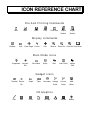
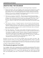
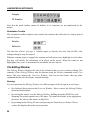
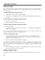
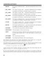
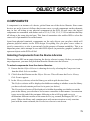
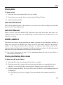
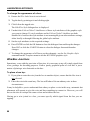
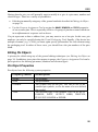
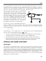
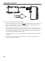
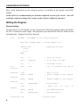
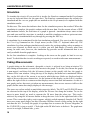
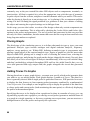
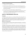
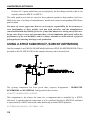
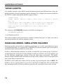
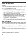
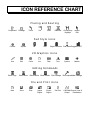
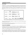
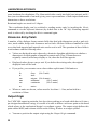
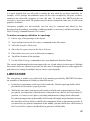
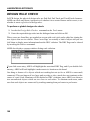
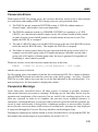
ICON REFERENCE CHART
File And Printing Commands
New
Open
Save
Print
Print Area
Import
Section
Export
Section
Display commands
Redraw
Grid
False Origin Cursor
Pan
Zoom In
Zoom Out View All View Area
Main Mode Icons
Component
Junction
Dot
Wire Label
Script
Bus
Sub-Circuit
Instant
Edit
Gadget Icons
Terminal
Device
Pin
Graph
Tape
Generator Voltage
Probe
Current
Probe
Multi
Meter
Symbol
Marker
2D Graphics
Line
Box
Circle
Arc
2D Path
Text
Design Tools
Real Time Snap
New Sheet
Wire Autorouter
Delete Sheet
Bill of Material
Search & Tag
Goto Sheet
Property Assignment Tool
Zoom to Child
Electrical Rules Check
Return to Parent
Netlist to Ares
Editing Commands
These affect all currently tagged objects.
Block Copy Block Move Block Delete Block Rotate Pick Device/Symbol Make Device Decompose
Package Tool
Undo
Redo
Cut
Copy
Paste
Rotate And Mirror Icons
Rotate Clockwise
Rotate Anti-clockwise
Flip X axis
Flip Y axis
TABLE OF CONTENTS
INTRODUCTION...................................................................................... 1
ABOUT ISIS.......................................................................................................................1
ISIS AND PCB DESIGN....................................................................................................2
ISIS AND SIMULATION.................................................................................................2
ISIS AND NETWORKS....................................................................................................4
HOW TO USE THIS DOCUMENTATION....................................................................4
TUTORIAL ................................................................................................ 5
INTRODUCTION ..............................................................................................................5
A GUIDED TOUR OF THE ISIS EDITOR......................................................................5
PICKING, PLACING AND WIRING UP COMPONENTS ...........................................7
LABELLING AND MOVING PART REFERENCES .....................................................9
BLOCK EDITING FUNCTIONS ....................................................................................11
PRACTICE MAKES PERFECT .....................................................................................11
ANNOTATING THE DIAGRAM .................................................................................12
The Property Assignment Tool (PAT).......................................................12
The Automatic Annotator............................................................................13
CREATING NEW DEVICES...........................................................................................14
FINISHING TOUCHES ...................................................................................................16
SAVING, PRINTING AND PLOTTING........................................................................17
MORE ABOUT CREATING DEVICES.........................................................................17
Making a Multi-Element Device..................................................................17
The Visual Packaging Tool...........................................................................19
Making Similar Devices................................................................................21
Replacing Components in a design...............................................................21
SYMBOLS AND THE SYMBOL LIBRARY................................................................21
REPORT GENERATION.................................................................................................22
A LARGER DESIGN........................................................................................................22
GENERAL CONCEPTS .......................................................................25
SCREEN LAYOUT ..........................................................................................................25
The Menu Bar..............................................................................................25
The Toolbars................................................................................................25
The Editing Window ....................................................................................26
The Overview Window................................................................................27
The Object Selector......................................................................................28
LABCENTER ELECTRONICS
Co-ordinate Display.....................................................................................28
CO-ORDINATE SYSTEM ..............................................................................................28
False Origin ..................................................................................................30
The Dot Grid................................................................................................30
Snapping to a Grid .......................................................................................30
Real Time Snap ............................................................................................30
FILING COMMANDS ....................................................................................................31
Starting a New Design ..................................................................................31
Loading a Design ..........................................................................................32
Saving the Design .........................................................................................32
Back-up and Last Loaded Files ....................................................................32
Import / Export Section................................................................................33
Quitting ISIS.................................................................................................33
GENERAL EDITING FACILITIES.................................................................................33
Object Placement..........................................................................................33
Tagging an Object .........................................................................................34
Deleting an Object ........................................................................................34
Dragging an Object .......................................................................................34
Dragging an Object Label..............................................................................34
Resizing an Object........................................................................................35
Reorienting an Object ...................................................................................35
Editing an Object ..........................................................................................36
Editing an Object Label ................................................................................36
Copying all Tagged Objects .........................................................................37
Moving all Tagged Objects...........................................................................37
Deleting all Tagged Objects..........................................................................38
WIRING UP......................................................................................................................38
Wire Placement.............................................................................................38
The Wire Auto-Router.................................................................................38
Wire Repeat..................................................................................................39
Dragging Wires .............................................................................................39
THE AUTOMATIC ANNOTATOR.............................................................................41
Value Annotation .........................................................................................42
MISCELLANEOUS .........................................................................................................42
The Sheet Border..........................................................................................42
The Header Block.........................................................................................43
Send to Back / Bring to Front.......................................................................46
Keyboard Configuration...............................................................................46
GRAPHICS AND TEXT STYLES .......................................................49
INTRODUCTION ............................................................................................................49
TUTORIAL.......................................................................................................................50
ISIS
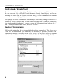
Editing Global Styles....................................................................................50
Editing Local Styles......................................................................................52
Working With The Template.......................................................................53
TEMPLATES AND THE TEMPLATE MENU............................................................54
PROPERTIES ........................................................................................55
INTRODUCTION ............................................................................................................55
OBJECT PROPERTIES....................................................................................................55
System Properties ........................................................................................55
User Properties ............................................................................................56
Property Definitions (PROPDEFS) ............................................................56
SHEET PROPERTIES ......................................................................................................57
Introduction..................................................................................................57
Defining Sheet Properties.............................................................................57
Scope Rules for Sheet Properties .................................................................58
DESIGN PROPERTIES ....................................................................................................60
PARAMETERIZED CIRCUITS.....................................................................................60
Introduction..................................................................................................60
An Example..................................................................................................61
Property Substitution ..................................................................................62
Property Expression Evaluation ..................................................................64
The Rounding Functions E12 (), E24 ().......................................................65
THE PROPERTY ASSIGNMENT TOOL......................................................................65
The PAT Dialogue Form..............................................................................66
PAT Actions ................................................................................................66
PAT Application Modes .............................................................................68
The Search and Tag Commands ...................................................................68
Examples ......................................................................................................69
PROPERTY DEFINITIONS ............................................................................................70
Creating Property Definitions......................................................................70
Default Property Definitions.......................................................................71
Old Designs..................................................................................................71
OBJECT SPECIFICS............................................................................73
COMPONENTS ...............................................................................................................73
Selecting Components from the Device Libraries ........................................73
Placing Components.....................................................................................74
Replacing Components ................................................................................75
Editing Components.....................................................................................75
Component Properties .................................................................................76
Hidden Power Pins.......................................................................................76
DOTS.................................................................................................................................76
Placing Dots .................................................................................................77
LABCENTER ELECTRONICS
Auto Dot Placement.....................................................................................77
Auto Dot Removal.......................................................................................77
WIRE LABELS.................................................................................................................77
Placing And Editing Wire Labels ..................................................................77
Deleting Wire Labels ....................................................................................78
Using a Wire Label to Assign a Net Name...................................................79
Using a Wire Label to Assign a Net Property..............................................79
Wire Label Properties...................................................................................79
SCRIPTS ...........................................................................................................................81
Placing and Editing Scripts...........................................................................81
Script Block Types ......................................................................................82
Part Property Assignments (*FIELD).........................................................82
Sheet Global Net Property Assignments (*NETPROP)............................83
Sheet Property Definitions (*DEFINE) ......................................................83
Parameter Mapping Tables (*MAP ON varname)......................................84
Model Definition Tables (*MODELS)........................................................84
Named Scripts (*SCRIPT scripttype scriptname)......................................85
SPICE Model Script (*SPICE) ....................................................................86
BUSES ...............................................................................................................................86
Placing Buses................................................................................................86
Bus Labels ....................................................................................................87
Wire/Bus Junctions ......................................................................................88
Bus Properties..............................................................................................89
SUB-CIRCUITS................................................................................................................89
Placing Sub-Circuits .....................................................................................89
Editing Sub-Circuits .....................................................................................91
Sub-Circuit Properties..................................................................................91
TERMINALS....................................................................................................................91
Logical Terminals .........................................................................................91
Physical Terminals .......................................................................................92
Placing Terminals .........................................................................................92
Editing Terminals .........................................................................................93
Terminal Properties......................................................................................94
PIN OBJECTS...................................................................................................................94
Placing Pin Objects.......................................................................................94
Editing Pin Objects.......................................................................................95
Pin Object Properties ...................................................................................95
SIMULATOR GADGETS...............................................................................................96
2D GRAPHICS .................................................................................................................96
Placing 2D Graphics.....................................................................................96
Resizing 2D Graphics ..................................................................................98
Editing 2D Graphics.....................................................................................99
ISIS
MARKERS .......................................................................................................................99
Marker Types ..............................................................................................99
Placing Markers..........................................................................................100
LIBRARY FACILITIES ........................................................................101
GENERAL POINTS ABOUT LIBRARIES..................................................................101
Library Discipline ......................................................................................101
The Pick Command....................................................................................101
SYMBOL LIBRARIES...................................................................................................102
Graphics Symbols ......................................................................................102
User Defined Terminals .............................................................................103
User Defined Module Ports.......................................................................104
User Defined Device Pins ..........................................................................106
Editing an Existing Symbol.........................................................................107
Hierarchical Symbol Definitions ................................................................107
DEVICE LIBRARIES .....................................................................................................107
Making a Device Element...........................................................................108
The Make Device Command......................................................................111
The Visual Packaging Tool.........................................................................116
Making a Single Element Device ................................................................119
Making a Multi-Element Homogenous Device..........................................120
M aking a Multi-Element Heterogeneous Device .......................................121
Making a Device with Bus Pins.................................................................122
Property Definitions and Default Properties.............................................123
Dealing with Power Pins............................................................................124
Editing an Existing Device..........................................................................126
MULTI-SHEET DESIGNS ..................................................................129
MULTI-SHEET FLAT DESIGNS.................................................................................129
Introduction................................................................................................129
Design Menu Commands...........................................................................129
HIERARCHICAL DESIGNS.........................................................................................129
Introduction................................................................................................129
Terminology ...............................................................................................130
Sub-Circuits................................................................................................131
Module-Components.................................................................................132
External Modules .......................................................................................133
Moving About a Hierarchical Design .........................................................133
Design Global Annotation..........................................................................134
Non-Physical Sheets ..................................................................................134
NETLIST GENERATION ....................................................................135
INTRODUCTION ..........................................................................................................135
LABCENTER ELECTRONICS
NET NAMES..................................................................................................................135
DUPLICATE PIN NAMES ...........................................................................................136
HIDDEN POWER PINS ................................................................................................136
SPECIAL NET NAME SYNTAXES............................................................................137
Global Nets ................................................................................................137
Inter-Element Connections for Multi-Element Parts.................................138
BUS CONNECTIVITY RULES .....................................................................................139
The Base Alignment Rule...........................................................................139
Using Bus Labels to Change the Connectivity Rule ..................................139
Using Bus Terminals to Interconnect Buses ..............................................140
Connections to Individual Bits...................................................................141
Tapping a Large Bus ..................................................................................143
General Comment & Warning....................................................................143
GENERATING A NETLIST FILE ................................................................................144
Format ........................................................................................................144
Logical/Physical/Transfer...........................................................................144
Scope..........................................................................................................144
Depth .........................................................................................................144
Errors..........................................................................................................145
NETLIST FORMATS....................................................................................................145
SDF ............................................................................................................145
BOARDMAKER ......................................................................................145
EEDESIGNER ...........................................................................................145
FUTURENET............................................................................................145
MULTIWIRE ............................................................................................145
RACAL......................................................................................................146
SPICE.........................................................................................................146
SPICE-AGE FOR DOS .............................................................................146
TANGO .....................................................................................................146
VALID .......................................................................................................146
VUTRAX...................................................................................................146
REPORT GENERATION ....................................................................147
BILL OF MATERIALS .................................................................................................147
Generating the Report ................................................................................147
Report Formats..........................................................................................147
Bill Of Materials Configuration .................................................................148
Adding Bill of Materials Parts ...................................................................154
ASCII DATA IMPORT ................................................................................................155
The IF...END Command............................................................................156
The DATA...END Command....................................................................157
ELECTRICAL RULES CHECK.....................................................................................159
ISIS
Generating the Report ................................................................................159
ERC Error Messages ..................................................................................159
HARD COPY GENERATION .............................................................163
PRINTER OUTPUT.......................................................................................................163
Specifying a Printer Device........................................................................163
Print Preview..............................................................................................163
Configuring Margins...................................................................................163
Scaling.........................................................................................................164
PLOTTER OUTPUT......................................................................................................164
Plotter Pen Colours....................................................................................165
CLIPBOARD AND GRAPHICS FILE GENERATION..............................................165
Bitmap Generation.....................................................................................165
Metafile Generation ...................................................................................165
DXF File Generation..................................................................................165
EPS File Generation ...................................................................................166
ISIS AND ARES ...................................................................................167
INTRODUCTION ..........................................................................................................167
PACKAGING.................................................................................................................167
Default Packaging.......................................................................................167
Manual Packaging.......................................................................................168
Automatic Packaging..................................................................................168
Using the Bill of Materials to Help with Packaging...................................169
The Package Verifier...................................................................................170
Packaging with ARES.................................................................................170
NET PROPERTIES AND ROUTING STRATEGIES .................................................170
FORWARD ANNOTATION - ENGINEERING CHANGES.....................................171
Adding New Components..........................................................................171
Removing Existing Components ................................................................172
Changing the connectivity..........................................................................172
Re-Annotating Components, and Re-Packaging Gates ..............................173
PIN-SWAP/GATE-SWAP ...........................................................................................173
Specifying Pin-Swaps and Gate-Swaps for ISIS Library Parts .................174
Specifying Pin-Swaps in Single Element Devices ......................................174
Specifying Pin-Swaps in Multi-Element Devices ......................................175
Specifying Gate-Swaps in Multi-Element Devices....................................175
Performing Manual Pin-Swaps and Gate-Swaps in ARES........................176
The Gate-Swap Optimizer.........................................................................177
RE-ANNOTATION.......................................................................................................179
BACK-ANNOTATION WITH ISIS............................................................................180
Semi-Automatic Back-Annotation.............................................................180
Fully-Automatic Back-Annotation............................................................180
LABCENTER ELECTRONICS
INDEX ....................................................................................................181
INTRODUCTION
ABOUT ISIS
Many CAD users dismiss schematic capture as a necessary evil in the process of creating
PCB layout but we have always disputed this point of view. With PCB layout now offering
automation of both component placement and track routing, getting the design into the
computer can often be the most time consuming element of the exercise. And if you use
circuit simulation to develop your ideas, you are going to spend even more time working on
the schematic.
ISIS has been created with this in mind. It has evolved over twelve years research and
development and has been proven by thousands of users worldwide. The strength of its
architecture has allowed us to integrate first conventional graph based simulation and now –
with PROTEUS VSM – interactive circuit simulation into the design environment. For the first
time ever it is possible to draw a complete circuit for a micro-controller based system and then
test it interactively, all from within the same piece of software. Meanwhile, ISIS retains a host
of features aimed at the PCB designer, so that the same design can be exported for production
with ARES or other PCB layout software.
For the educational user and engineering author, ISIS also excels at producing attractive
schematics like you see in the magazines. It provides total control of drawing appearance in
turns of line widths, fill styles, colours and fonts. In addition, a system of templates allows
you to define a ‘house style’ and to copy the appearance of one drawing to another.
Other general features include:
•
Runs on Windows 98/Me/2k/XP and later.
•
Automatic wire routing and dot placement/removal.
•
Powerful tools for selecting objects and assigning their properties.
•
Full support for buses including component pins, inter-sheet terminals, module ports
and wires.
•
Bill of Materials and Electrical Rules Check reports.
•
Netlist outputs to suit all popular PCB layout tools.
1
LABCENTER ELECTRONICS
For the ‘power user’, ISIS incorporates a number of features which aid in the management of
large designs. Indeed, a number of our customers have used it to produce designs containing
many thousands of components.
•
Hierarchical design with support for parameterized component values on sub-circuits.
•
Design Global Annotation allowing multiple instances of a sub-circuit to have different
component references.
•
Automatic Annotation - the ability to number the components automatically.
•
ASCII Data Import - .this facility provides the means to automatically bring component
stock codes and costs into ISIS design or library files where they can then be
incorporated or even totalled up in the Bill of Materials report.
ISIS AND PCB DESIGN
Users of ARES, or indeed other PCB software will find some of the following PCB design
specific features of interest:
•
Sheet Global Net Properties which allow you to efficiently define a routing strategy for
all the nets on a given sheet (e.g. a power supply needing POWER width tracks).
•
Physical terminals which provide the means to have the pins on a connector scattered
all over a design.
•
Support for heterogeneous multi-element devices. For example, a relay device can have
three elements called RELAY:A, RELAY:B and RELAY:C. RELAY:A is the coil whilst
elements B and C are separate contacts. Each element can be placed individually
wherever on the design is most convenient.
•
Support for pin-swap and gate-swap. This includes both the ability to specify legal
swaps in the ISIS library parts and the ability to back-annotate changes into a
schematic.
•
A visual packaging tool which shows the PCB footprint and its pin numbers alongside
the list of pin names for the schematic part. This facilitates easy and error free
assignment of pin numbers to pin names. In additional, multiple packagings may be
created for a single schematic part.
A full chapter is provided on how to use ISIS and ARES together.
ISIS AND SIMULATION
ISIS provides the development environment for PROTEUS VSM, our revolutionary interactive
system level simulator. This product combines mixed mode circuit simulation, micro-processor
2
ISIS
models and interactive component models to allow the simulation of complete micro-controller
based designs.
ISIS provides the means to enter the design in the first place, the architecture for real time
interactive simulation and a system for managing the source and object code associated with
each project. In addition, a number of graph objects can be placed on the schematic to enable
conventional time, frequency and swept variable simulation to be performed.
Major features of PROTEUS VSM include:
•
True Mixed Mode simulation based on Berkeley SPICE3F5 with extensions for digital
simulation and true mixed mode operation.
•
Support for both interactive and graph based simulation.
•
CPU Models available for popular microcontrollers such as the PIC and 8051 series.
•
Interactive peripheral models include LED and LCD displays, a universal matrix keypad,
an RS232 terminal and a whole library of switches, pots, lamps, LEDs etc.
•
Virtual Instruments include voltmeters, ammeters, a dual beam oscilloscope and a 24
channel logic analyser.
•
On-screen graphing - the graphs are placed directly on the schematic just like any other
object. Graphs can be maximised to a full screen mode for cursor based measurement
and so forth.
•
Graph Based Analysis types include transient, frequency, noise, distortion, AC and DC
sweeps and fourier transform. An Audio graph allows playback of simulated waveforms.
•
Direct support for analogue component models in SPICE format.
•
Open architecture for ‘plug in’ component models coded in C++ or other languages.
These can be electrical., graphical or a combination of the two.
•
Digital simulator includes a BASIC-like programming language for modelling and test
vector generation.
•
A design created for simulation can also be used to generate a netlist for creating a PCB
- there is no need to enter the design a second time.
Full details of all these features and much more are provided in the PROTEUS VSM manual.
3
LABCENTER ELECTRONICS
ISIS AND NETWORKS
ISIS is fully network compatible, and offers the following features to help Network Managers:
•
Library files can be set to Read Only. This prevents users from messing with symbols or
devices that may be used by others.
•
ISIS individual user configuration in the windows registry. Since the registry determines
the location of library files, it follows that users can have individual USERDVC.LIB files
in their personal or group directories.
HOW TO USE THIS DOCUMENTATION
This manual is intended to complement the information provided in the on-line help. Whereas
the manual contains background information and tutorials, the help provides context
sensitive information related to specific icons, commands and dialog forms. Help on most
objects in the user interface can be obtained by pointing with the mouse and pressing F1.
ISIS is a vast and tremendously powerful piece of software and it is unreasonable to expect to
master all of it at once. However, the basics of how to enter a straightforward circuit diagram
and create your own components are extremely simple and the techniques required for these
tasks can be mastered most quickly by following the tutorial given in Tutorial on page 5. We
strongly recommend that you work through this as it will save you time in the long run.
With some of the more advanced aspects of the package, you are probably going to find
some of the concepts are new, let alone the details of how ISIS handles them. Each area of the
software has been given a chapter of its own, and we generally start by explaining the
background theory before going into the operation and use of the relevant features. You will
thus find it well worthwhile reading the introductory sections rather than jumping straight to
the how-to bits.
4
TUTORIAL
INTRODUCTION
The aim of this tutorial is to take you through the process of entering a circuit of modest
complexity in order to familiarise you with the techniques required to drive ISIS. The tutorial
starts with the easiest topics such as placing and wiring up components, and then moves on
to make use of the more sophisticated editing facilities, such as creating new library parts.
For those who want to see something quickly, ISISTUT.DSN contains the completed tutorial
circuit. This and other sample designs are installed to the SAMPLES directory.
Note that throughout this tutorial (and the documentation as a whole) reference is made to
keyboard shortcuts as a method of executing specific commands. The shortcuts specified are
the default or system keyboard accelerators as provided when the software is shipped to you.
Please be aware that if you have configured your own keyboard accelerators the shortcuts
mentioned may not be valid. Information on configuring your own keyboard shortcuts can be
found in the section on Keyboard Configuration on page 46.
A GUIDED TOUR OF THE ISIS EDITOR
We shall assume at this point that you have installed the package, and that the current
directory is some convenient work area on your hard disk.
To start the ISIS program, click on the Start button and select Programs, Proteus 6
Professional, and then the ISIS 6 Professional option. The ISIS schematic editor will then
load and run. Along the top of the screen is the Menu Bar.
The largest area of the screen is called the Editing Window, and it acts as a window on the
drawing - this is where you will place and wire-up components. The smaller area at the top
right of the screen is called the Overview Window. In normal use the Overview Window
displays, as its name suggests, an overview of the entire drawing - the blue box shows the
edge of the current sheet and the green box the area of the sheet currently displayed in the
Editing Window. However, when a new object is selected from the Object Selector the
Overview Window is used to preview the selected object - this is discussed later.
You can adjust the area of the drawing displayed in the Editing Window in a number of ways:
•
To simply 'pan' the Editing Window up, down, left or right, position the mouse pointer
over the desired part of the Editing Window and press the F5 key.
•
Hold the SHIFT key down and bump the mouse against the edges of the Editing
Window to pan up, down, left or right. We call this Shift Pan.
5
LABCENTER ELECTRONICS
•
Should you want to move the Editing Window to a completely different part of the
drawing, the quickest method is to simply point at the centre of the new area on the
Overview Window and click left.
•
You can also use the Pan icon on the toolbar.
To adjust the scale the drawing is displayed at in the Editing Window you can:
•
Point with the mouse where you want to zoom in or out and press the F6 or F7 keys
respectively or else scroll the mouse wheel.
•
Press the F8 key to display the whole drawing.
•
Hold the SHIFT key down and drag out a box around the area you want to zoom in to.
We call this Shift Zoom..
•
Use the Zoom In, Zoom Out, Zoom Full or Zoom Area icons on the toolbar.
A grid of dots can be displayed in the Editing Window using the Grid command on the View
menu, or by pressing 'G', or by clicking the Grid icon on the toolbar. The grid helps in lining
up components and wires and is less intimidating than a blank screen. If you find it hard to
see the grid dots, either adjust the contrast on your monitor slightly (by default the grid dots
are displayed in light grey) or change their colour with the Set Design Defaults on the
Template menu.
Below the Overview Window is the Object Selector which you use to select devices, symbols
and other library objects.
At the bottom right of the screen is the co-ordinate display, which reads out the co-ordinates
of the mouse pointer when appropriate. These co-ordinates are in 1 thou units and the origin
is in the centre of the drawing.
6
ISIS
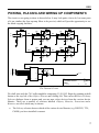
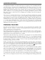
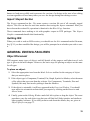
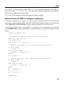
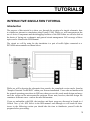
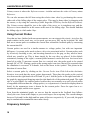
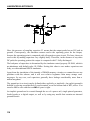
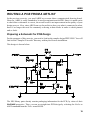
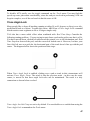
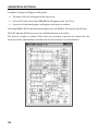
PICKING, PLACING AND WIRING UP COMPONENTS
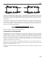
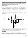
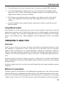
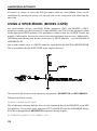
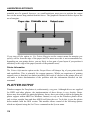
The circuit we are going to draw is shown below. It may look quite a lot to do, but some parts
of it are similar (the four op-amp filters to be precise) which will provide opportunity to use
the block copying facilities.
R2
R6
1K
R5
DAC2
56K
U2:A
3
1
2
TL074
U1
10K
56K
56K
U2:B
5
R9
11
R4
12K
R7
4
100K
DAC1
R10
15K
R3
7
6
TL074
R8
56K
741
R1
1K
C1
C2
C3
C4
220p
220p
220p
220p
R14
100K
U2:C
10
R13
68K
R18
15K
R11
8
9
TL074
R12
SW1
12K
R15
10K
68K
68K
U2:D
12
R17
14
13
TL074
R16
68K
C5
C6
C7
C8
1n5
1n5
1n5
1n5
U3
FROM PIO-1A
15
DA0
DA1
DA2
DA3
DA4
DA5
8
7
6
5
4
3
13
12
11
9
VIN
D0
D1
D2
D3
D4
D5
RFB
16
C9 U4
39p
IOUT
1
AUDIO OUT
S1
S2
S3
DGND
TL071
AGND
2
TITLE:
7110
DATE:
TUTORIAL CIRCUIT
MAIN
BY:
LABCENTER
01-Mar-96
PAGE:
REV:
1/1
The Tutorial Circuit
We shall start with the 741 buffer amplifier comprising U1, R1, R2. Begin by pointing at the P
button at the top left of the Object Selector and clicking left. This causes the Device Library
Selector dialogue form to appear and you can now select devices from the various device
libraries. There are a number of selectors labelled Objects, Libraries, Extensions and a
Browser, not all of which may be shown:
•
The Library selector chooses which of the various device libraries (e.g. DEVICE, TTL,
CMOS) you have installed is current.
7
LABCENTER ELECTRONICS
•
The Objects selector displays all the parts in the currently selected library according to
the settings in the Extensions selector, if it is shown (see below). Click left once on a
part to browse it or double-click a part to ‘pick’ it in to the design.
•
The Browser displays the last selected part in the Parts selector as a means of browsing
the contents of the library.
We need two devices initially - OPAMP for the 741 op-amp and RES for the feedback
resistors. Both these are in the DEVICE library, so, if it is not already selected, start by
selecting the DEVICE library in the Library selector. Then, double-click on the OPAMP and
RES parts from the Parts selector to select each part. The devices you have picked should
appear in the Object Selector.
Whenever you select a device in the Devices selector or use the Rotation or Mirror icons to
orient the device prior to placement, the selected device is shown previewed in the Overview
Window with the orientation the selected device will have if placed. As you click left or right
on the Rotation and/or Mirror icons, the device is redrawn to preview the new orientation.
The preview remains until the device is placed or until the another command or action is
performed.
Ensure the OPAMP device is selected and then move the mouse pointer into the middle of the
Editing Window. Press and hold down the left mouse button. An outline of the op-amp will
appear which you can move around by dragging the mouse. When you release the button,
the component will be placed and is drawn in full. Place the op-amp in the middle of the
Editing Window. Now select the RES device and place one resistor just above the op-amp as
in the diagram and click left once on the anti-clockwise Rotation icon; the preview of the
resistor shows it rotated through 90°. Finally, place the second (vertical) resistor, R1 as
before.
Unless you are fairly skilful, you are unlikely to have got the components oriented and
positioned entirely to your satisfaction at this first attempt, so we will now look at how to
move things around. In ISIS, objects are selected for further editing by 'tagging' them. Try
pointing at the op-amp and clicking right. This tags the object, causing it to be highlighted.
Now, still keeping the pointer over it, hold the left button down and drag it around. This is
one of the ways to move objects. Release the left button, and click right on the op-amp a
second time. Clicking right on a tagged object deletes it. Select Undo on the Edit Menu (or
press 'U') to recover it. Tag it again, and click first left and then right on the Rotation icon
whilst watching the op-amp itself. The rotation of the last object you tagged can be adjusted
in this way; the Mirror icon can similarly be used to reflect the last object tagged. Armed with
the above knowledge, you should now be able to adjust the three components you have
placed such that they match the diagram. When you have finished editing, point at a free
space in the Editing Window (i.e. somewhere where there is no object) and click right to untag all tagged objects.
8
ISIS
We can now move on to place some wires. Start by pointing at the tip of the upper end of R1
and clicking left. ISIS senses that you are pointing at a component pin and deduces that you
wish to connect a wire from it. To signify this, it displays a green line which goes from the pin
to the pointer. Now point at the tip of the inverting input of the op-amp and click left again.
ISIS takes this as the other end for the wire and invokes the Wire Auto Router (WAR) to
choose a route for the wire. Now do the same thing for each end of R2, following the diagram.
Try tagging objects and moving them around whilst observing how the WAR re-routes the
wires accordingly.
If you do not like a route that the Wire Auto Router has chosen, you can edit it manually. To
do this, tag the wire (by pointing at it and clicking right) and then try dragging it first at the
corners and then in the middle of straight runs. If you want to manually route a wire you can
do so by simply clicking left on the first pin, clicking left at each point along the required
route where you want a corner, and then finish by clicking left on the second pin. After a
while, you will get a feel for when the WAR will cope sensibly and when you will need to take
over.
To complete this first section of the drawing, you need to place the two generic and one
ground terminals and wire them up. To do this, select the Terminal icon; the Object Selector
changes to a list of the terminal types available. Select the Ground terminal, ensure its
preview shows it correctly oriented, and place it just under R1. Now select the Default
terminal from the selector and place two terminals as in the diagram. Finally wire the ground
terminal to the bottom of R1 and the two default terminals to the corners of the wires going
into the op-amp. ISIS will place the junction dots where required, sensing automatically that
three wires are meeting at these points.
LABELLING AND MOVING PART REFERENCES
ISIS has a very powerful feature called Real Time Annotation which can be found on the
Tools Menu and is enabled by default. Full information can be found on page 12 but basically,
when enabled, this feature annotates components as you place them on the schematic. If you
zoom in on any resistor you have placed you will see that ISIS has labelled it with both the
default value (RES) and a unique reference. To edit/input part references and values click left
on the Instant Edit icon and then click left on the object you wish to edit. Do the resistors
first, entering R1, 1k and R2, 1k as appropriate. Now do the op-amp and the two terminals.
To move the 'U1' and the '741' labels to correspond with the diagram, press F2 to reduce the
snapping grid to 50th (it starts off at 100th) and then tag the op-amp. Now point at the label
'U1' and with the left button depressed, drag it to its correct position under the op-amp. Then
do the same with the '741' label.
When you have finished positioning the labels, put the snap back to 100th by pressing F3.
Although with the Real Time Snap feature ISIS is able to locate pins and wires not on the
9
LABCENTER ELECTRONICS
current snap grid, working consistently with the same snap grid will keep drawings looking
neat and tidy.
10
ISIS
BLOCK EDITING FUNCTIONS
You may have noticed that the section of circuit you have drawn so far is currently located in
the middle of the sheet, whereas it should be in the top left hand corner. To move it there, first
tag all the objects you have placed by dragging a box round them using the right mouse
button: point at a position above and to the left of all the objects; then press and hold down
the right button and drag the mouse pointer to a position below and to the right of the
objects. The selected area is shown by a cyan tag-box and (as the initial right click
automatically untags any previously tagged objects) all and only those objects wholly within
the tag-box will be tagged after the operation.
Now click left on the Block Move icon. A box will appear round all the tagged objects, and
you can now begin to move this up towards the top left hand corner of the sheet. The sheet
border appears in dark blue so you can now re-position the buffer circuit up at the top left of
the drawing. Click left to effect the move, or else you can abort it by clicking right. You should
also note how, when you moved the pointer off the Editing Window to the top or left, ISIS
automatically panned the Editing Window for you. If you want to pan like this at other times
(i.e. when not placing or dragging an object), you can use the Shift Pan feature.
The group of objects you have moved will remain tagged, so you might as well experiment
with the Copy and Delete icons which similarly operate on the currently tagged objects. The
effect of these icons can be cancelled by immediately following their use by pressing the 'U'
key for Undo.
PRACTICE MAKES PERFECT
You should be getting the hang of things now, so get some more practice in by drawing the
next section of circuitry centred around the op-amp U2:A. You will need to get a capacitor
(CAP). A quick method of picking devices whose names you know is to use the Pick
Device/Symbol command. Press the 'P' key (for Pick Device/Symbol) and then type in the
name - CAP. Use the various editing techniques that have been covered so far to get
everything in the right place. Move the part reference and value fields to the correct
positions, but do not annotate the parts yet - we are going to use the Automatic Annotator
to do this.
When you have done one op-amp filter to you satisfaction, use a tag-box and the Block
Copy icon to make three copies - four filters in all - as there are in the diagram. You may find it
useful to use the zoom commands on the View menu (or their associated short-cut keys) so as
to be able to see the whole sheet whilst doing this. When you have the four filters in position,
wire them together, and place a SW-SPDT device (SW1) on the drawing.
11
LABCENTER ELECTRONICS
ANNOTATING THE DIAGRAM
ISIS provides you with four possible approaches to annotating (naming) components:
•
Manual Annotation - This is the method you have already used to label the first op-amp
and resistors. Any object can be edited either by selecting the Instant Edit icon and
then clicking left on it, or by clicking right then left on it in the normal placement mode.
Whichever way you do it, a dialogue box then appears which you can use to enter the
relevant properties such as Reference, Value and so forth.
•
The Property Assignment Tool (PAT) - This tool can generate fixed or incrementing
sequences and assign the resulting text to either all objects, all tagged objects (either on
all sheets or the current sheet) or to the objects you subsequently click left on. Using
the PAT is faster than manual annotation, though slower than using the Automatic
Annotator. However, it does leave you in control of which names are allocated to which
parts.
•
The Automatic Annotator - Using the Automatic Annotator leads to the whole design
being annotated in a matter of seconds. The tool is aware of multi-element parts like the
7400 TTL NAND gate package and will allocate gates appropriately. However, the whole
process is non-interactive so you get far less control over the names that are allocated
than with the other two methods.
•
Real Time Annotation – This feature, when enabled, will annotate components as you
place them on the design , obviating any need for you to place references and values in
your design. As with the Automatic Annotator, however, it makes the whole process
non-interactive and offers no user control over the annotation process. Real Time
Annotation can be toggled on and off through the Real Time Annotation command on
the Tools Menu or via the shortcut key (default mapping is CTRL+N – more
information on shortcut keys is given on page 46).
In practice you can use a mix of all four methods, and in any order you choose. The
Automatic Annotator can be set to leave alone any existing annotation so that it is possible
to fix the references of certain parts and then let ISIS annotate the rest by itself. As the Real
Time Annotation is enabled by default, we shall leave it on and use the other three methods
to edit the existing annotation of the design.
The Property Assignment Tool (PAT)
Let us suppose, for the sake of argument, that you wished to pre-annotate all the resistors
using the PAT. Given that you have already manually annotated R1 and R2, you need to
generate the sequence R3, R4, R5 etc. To do this, select the Property Assignment Tool option
on the Tools menu. Enter REF=R# in the String field, then move the cursor to the next field
(the Count field) and key in the value 3. Ensure the On Click button is selected and then click
12
ISIS
left on the OK button or press ENTER. The hash-character ('#') in the String field text will be
replaced with the current Count field value each time the PAT assigns a string to an object
and then the Count field value is incremented.
ISIS automatically selects the Instant Edit icon so that you can annotate the required objects
by clicking left on them. Point at resistor R3 and click left. The PAT supplies the R3 text and
the part is redrawn. Now do the same for the resistor below it, R4 and see how the PAT's
Count field value increments each time you use it. You can now annotate the rest of the
resistor references with some panache. When you are done with this, cancel the PAT, by
calling up its dialogue form (use the 'A' keyboard shortcut for speed) and then either clicking
on the CANCEL button or by pressing ESC.
The PAT can also be used to assign the same String to several tagged objects, for example
the part values of resistors or capacitors that all have the same value. Consider the capacitors
C1 to C4 which all have the value 220p. To assign this value, first ensure that only the
capacitors are tagged by first clicking right on a free area of the Edit Window to untag all
objects, then clicking right on each capacitor. Now invoke the PAT and enter VAL=220p in
the String field, select the Local Tagged button and click OK. That's it - you do not need to
cancel the PAT as it is not in its 'On Click' assignment mode.
Try this on your own for the rest of the diagram until you are clear about how the PAT works
- although a little tricky at first, it is an extremely powerful tool and can eliminate a great deal
of tedious editing. Do not forget that, when used in its On Click mode, you need to cancel
the tool when finished.
The Automatic Annotator
ISIS features an automatic annotator which will choose component references for you. It can
be made to annotate all the components, or just the ones that haven't yet been annotated - i.e.
those with a '?' in their reference.
Since you have already annotated some of the parts, we will run the Automatic Annotator in
'Incremental' mode. To do this, invoke the Global Annotator command on the Tools menu,
click on the Incremental button, and then click on OK. After a short time, the diagram will be
re-drawn showing the new annotation. Since the OPAMP device is not a multi-element part
like a true TL074, the annotator annotates them as U2 to U5 which is not what is wanted. To
correct this, edit each one in turn and key in the required reference. We will see how to create
and use a proper TL074 later on.
Even with the automatic annotator, you still have to set the component values manually, but
try this for speed - instead of moving around the drawing to edit each component in turn,
simply key 'E' for Edit Component (on the Edit menu) and key in a component's reference.
This automatically locates the desired part and brings up its Edit... dialogue form. You should
also try out the using the Property Assignment Tool as described in the above section.
13
LABCENTER ELECTRONICS
CREATING NEW DEVICES
The next section of the circuit employs a 7110 digital attenuator, and this provides an
opportunity to learn how to make new devices in ISIS.
In ISIS new devices are created directly on the drawing - there is no separate device editor
mode, let alone a separate program. The new device is created by placing a collection of 2D
graphics and pins, annotating the pins, and then finally tagging them all and invoking the
Make Device command.
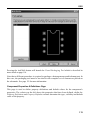
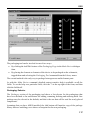
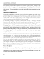
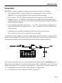
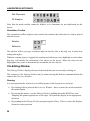
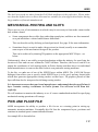
You will find it helpful when creating new devices to sketch
out on paper how you want the device to look, and to
establish roughly how big it needs to be by considering
how may pins there will be down each side and so on. In
this case you can use the diagram opposite as a guide. The
first thing we need to do is to locate a free area of your
design where the new device can be created - click the left
mouse button on the lower-right region of the Overview
Window to position the Editing Window on that area of the
design.
Begin by drawing the device body of the new device. Select the Box icon. You will see that
the Object Selector on the right displays a list of Graphics Styles. A graphics style
determines how the graphic we are about to draw will appear in terms of line colour, line
thickness, fill style, fill colour, etc. Each style listed is a different set of such attributes and
define the way different parts of the schematic appear.
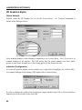
ISIS supports a powerful graphics style system of local and global styles and the ability of
local styles to ‘follow’ or ‘track’ global styles that allows you to easily and flexibly customise
the appearance of your schematic. See the section Graphics And Text Styles on page 49 for a
complete explanation of how styles work and how they are used.
As we are drawing the body of a component, select the COMPONENT graphics style and
then place the mouse pointer over the Editing Window, press and hold down the left mouse
button and drag out a rectangle. Don't worry about getting the size exactly right - you can
always resize the rectangle later. You will see that, as a result of choosing the COMPONENT
graphics style, the rectangle appears in the same colour, fill, etc. as all the other components
on the schematic.
The next thing to do is to place the pins for the new device. To do this, first select the the
Device Pin icon. The Object Selector lists the types of available pins (note that you can also
create your own pin objects in ISIS, though we will not cover that in this tutorial). Select the
Default pin type from the selector; the Overview Window provides a preview of the pin with
the pin's name and number represented by the strings NAME and 99 and its base and end
14
ISIS
indicated by an Origin marker and cross respectively - the cross represents the end to which
you will eventual connect a wire. Use the Rotation and Mirror icons to orient the pin preview
ready to place the left-hand pins and then click the left mouse button in the Editing Window
on the left edge of the rectangle where you want each pin's base to appear. Place pins for the
VIN, D0..D5, S1..3 and DGND pins. Note that you can use the DOWN key to move the mouse
pointer down one grid square and the ENTER key as a substitute for the left mouse button - it
is sometimes quicker to use these keys instead of the mouse. Now click left on the Mirror
icon and then place the three right-hand pins: RFB, IOUT and AGND. To finish, place two
pins, one on the top edge and one on the bottom edge of the rectangle, adjusting the
Rotation and Mirror icons before placing them in order that they point outwards from the
device body; these pins will be the VDD and VBB power pins and will eventually be hidden
(this is why they are not shown in the figure).
At this stage, you can reposition the pins or resize the rectangle as required. To move a pin,
tag it with the right mouse button and then drag it with the left button; to re-orient it, use the
Rotation and Mirror icons. To adjust the size of the device body rectangle, tag it with the
right mouse button, click and hold down the left mouse button on one of the eight 'drag
handles' (the small white boxes at the corners and mid-points of the rectangle's edges) and
drag the handle to the new position. If you adjust its width, you will also need to draw a tagbox (with the right mouse button) around the pins and then use the Move icon to re-position
them.
So, having arranged the device body rectangle and pins as required, we now need to annotate
the pins with names and numbers, and to assign them an electrical type. The electrical type
(input, power, pull-up, etc.) is used by the Electrical Rules Check to ensure that only pins
with the correct electrical type are inter-connected.
We will first assign names, electrical types and visibility. To do this, we have to tag each pin
by clicking right on it and then edit it by clicking left on the tagged pin; the pin displays its
Edit Pin dialogue form.
Edit each pin in turn, as follows:
•
Enter the pin's name in the Name field. Leave the Number field empty as we will assign
the pin numbers with the Property Assignment Tool.
•
Select the appropriate electrical type for the pin - Output for the IOUT pin, Power for the
VDD, VBB, AGND and DGND pins, and Input for the remainder.,
•
Select whether the pin is to be hidden by unchecking its Draw body checkbox - the
VDD and VBB pins are both standard power pins and can be hidden. The AGND and
DGND pins are non-standard and so need to remain visible in order that they can be
wired up as appropriate to the design the device is being used in.
•
Select the OK button when finished.
15
LABCENTER ELECTRONICS
To assign the pin numbers, we will use the Property Assignment Tool. To initialise the PAT,
select the Property Assignment Tool command from the Tools Menu, and enter NUM=# in the
String field and the value 1 in the Count field. Select the On Click button, and then close the
dialogue form with the OK button. Now carefully click on each pin in order of its number
(IOUT, AGND, etc.). As you click on each pin, it is assigned a pin number by the PAT. When
done, don't forget to cancel the PAT by bringing up its dialogue form and selecting the
CANCEL button.
All we do now is actually make the device. To do this, tag all the pins and the body rectangle
- the easiest way is to drag out a tag-box with the right mouse button around the whole area
being careful not to miss out the two hidden power pins. Finally, select the Make Device
command from the Library menu to display the Make Device dialogue form. Key in the name
7110 in the Name field and the letter U in the Prefix field. Then press the Next button until
the list of writable device libraries is displayed, select an appropriate library and then click the
OK button to save the new device.
FINISHING TOUCHES
Now that you have defined a 7110 you can place, wire up and annotate the remainder of the
diagram - use the Automatic Annotator in Incremental mode to annotate the new parts
without disturbing the existing annotation.
The labelling and bracket around the six input terminals DA0-DA5 is done with 2D graphics.
ISIS provides facilities for placing lines, boxes, circles, arcs and text on your drawings; all of
which offered as icons on the Mode Selector toolbar.
The bracket is made from three lines - place these by selecting the Line icon and then clicking
at the start and end of each line. Then place the text FROM PIO-1A as shown by selecting
the Text icon, setting the Rotation icon to 90° and then clicking left at the point where to want
the bottom of the 'F' character to appear. You can of course tag and drag 2D graphics objects
around to get things just how you want.
Finally, you need to place a sheet border and a header block. To do the former, select the Box
icon, zoom out till you can see the whole sheet outline (dark blue) and then place a graphics
box over it. It is important to realise that the dark blue sheet outline does not appear on hard
copy - if you want a bounding box you must place one as a graphics object.
The header block is worthy of more discussion. It is, in fact, no different from other symbols
such as you might use for your company logo (see section [Symbols And The Symbol
Library] for more on symbols). A default header block called HEADER is provided but you
can re-define this to suit your own requirements - see The Header Block on page 43.
To actually place the header, select the Symbol icon and then click left on the P button of the
Object Selector to display the Symbol Library Selector dialogue form. Picking symbols from
16
ISIS
symbol libraries is similar to picking devices from device libraries except that there is no Prefix
selector. Select the HEADER object from the SYSTEM symbol library and close down the
dialogue form. With HEADER now the current symbol, point somewhere towards the bottom
left of the drawing, press the left mouse button, and drag the header into position.
Some of the fields in the header block will fill in automatically; others such as the Design Title,
Sheet Title, Author and Revision need to be entered using the Edit Design Properties and
Edit Sheet Properties commands on the Design menu. Note that the Sheet Name field on the
Edit Sheet Properties dialogue form is different from the Sheet Title - the Sheet Name is a
short label for the sheet that is used in hierarchical design. The Sheet Title is a full description
of the circuitry on that sheet and it is this that will appear in the header block.
You will need to zoom in on the header to see the full effects of your editing.
SAVING, PRINTING AND PLOTTING
You can save your work at any time by means of the Save command on the File menu, and
now is as good a time as any! The Save As option allows you to save it with a different
filename from the one you loaded it with.
To print the schematic, first select the correct device to print to using the Printer Setup
command on the File menu. This activates the Windows common dialogue for printer device
selection and configuration. The details are thus dependent on your particular version of
Windows and your printer driver - consult Windows and printer driver documentation for
details. When you have selected the correct printer, close the dialogue form and select the
Print option on the File menu to print your design. Printing can be aborted by pressing ESC,
although it may be a short time before everything stops as both ISIS and possibly your
printer/plotter have to empty their buffers.
Further details regarding printer and graphics output are given under Hard Copy Generation
on page 163.
If you have the demo version, please note that you can only print un-modified sample
designs. To try this now, use the Load command on the File menu to load a sample design.
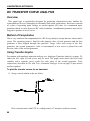
MORE ABOUT CREATING DEVICES
Making a Multi-Element Device
We shall now define a proper library part for the TL074 quad op-amp. As there are four
separate op-amps to a single TL074 package our tutorial will be showing you how to create
multi-element devices using the Visual Packaging Tool.
17
LABCENTER ELECTRONICS
The illustration on the left shows the new op-amp device before it is
made. The op-amp is made from some 2D graphics, five pins and an origin
marker. We will look at two ways to construct the op-amp graphics. The
easiest approach uses the pre -defined OPAMP symbol. Proceed as
follows:
•
Click on the Symbol icon and then click the P button at the top left of the Symbols
Object Selector. This will launch the Symbol Library Selector dialogue form.
•
Double-click on OPAMP in the System Library and close the dialogue form using the
Windows Minimise button on the right of the title bar.
•
Position the mouse pointer in an empty area of the Editing Window and use the left
mouse button to place the op-amp. The op-amp automatically appears in the
COMPONENT graphics style as this style was used to create the symbol.
Now place the pins around the component body. This is the same process as for creating the
7110 attenuator earlier:
•
Select the Device Pin icon to obtain a list of available pin types and select the Default
type.
•
Use the Rotate and Mirror icons to orient the pins before placing them on the design.
•
Once all the pins are in the correct positions, edit each pin in turn by tagging it with the
right mouse button and then clicking left on it. Use the resulting Edit Pin dialogue form
to annotate the pin with the correct electrical type and pin name. We have to give the
pins names so that we can reference them in the Packaging Tool however, we don't
want the name to be displayed (as the op-amp pins' uses are implicit from the graphics)
so ensure that the Draw Name check-box is not checked. Note, there is no need to
specify pin numbers as these will entered using the Packaging Tool.
The power pins have the names V+ and V- and have the electrical type of Power; if you place
them just in from the left edge of the op-amp, you will find they just touch the sloping sides of
the OPAMP graphic whilst keeping their pin ends (marked by an 'X') on a grid-square. If in a
similar situation, they didn't touch, you could 'extend' the base of the pin by placing short
lines in 2D Graphic Mode and with the mouse snap off. The input pins have the names +IP
and -IP and the electrical type Input. The output pin has the name OP and the electrical type
Output.
The final stage is to place an Origin marker. Select the Marker icon to display a list of system
marker symbols in the Object Selector. Select the Origin marker in the System Library and
then place the marker symbol at the centre of the op-amp graphics. The Origin marker is
18
ISIS
displayed as a rectangle with cross-hairs and it indicates to ISIS how the new device should
appear around the mouse pointer when the device is dragged or placed in a design.
We have now completed making the device. Tag the constituent parts - the op-amp symbol,
pins and the Origin marker - by dragging out a tag-box around them using the right mouse
button, and then invoke the Make Device command on the Library menu. Then proceed as
follows:
•
Enter the Device Name as TL074 and the Prefix as 'U'
•
Click Next button display the Packaging page and click Add/Edit to launch the
packaging tool itself.
The Visual Packaging Tool
The visual packaging tool provides a graphical environment in which to assign one or more
PCB footprints to a schematic part. For each packaging, a table of pin numbers to pin names is
created such that different packagings can have different pin numbers for the same schematic
pin.
Having launched the packaging tool, the first thing to do is to create a packaging:
•
Click the Add button. This will launch the ARES library browser.
•
Select the PACKAGE library, and double click the DIL14 part.
Then, you need to make the following changes to the default settings for the packaging:
•
Change the number of elements from 1 to 4. This corresponds with the fact that there are
four op-amps within the one physical DIL14 package.
•
Mark the V+ and V- pins as common pins. This means that they will have the same pin
number on each element, and that you can wire to any or all of the pins on the elements
on the schematic. All such wiring will be deemed interconnected.
•
Click the Gates can be Swapped checkbox. This specifies that the elements are identical
and the ARES can perform gateswap operations on this part.
19
LABCENTER ELECTRONICS
You should then see a display similar to that below:
Now to assign the pin numbers. The actual pinning of the op-amps that we are aiming at is
shown below:
Proceed as follows:
•
Click left in the 'A' column box for pin +IP.
•
Either, click pin '3' on the package display or enter '3' from the keyboard and press TAB.
Either way, pin '3' will highlight on the package to show that you have assigned it, and
the cursor will move to the -IP row.
20
ISIS
•
Now, repeat the process for the other pin numbers, until all the pins on the package
display are highlighted. This of course, provides a visual cue that you haven't missed
any pins.
Finally, click the Assign Packages button to return the Make Device wizard, and then store
the device into your USERDVC library, as you did with the 7110.
There is, as you have probably realized, a great deal of functionality built into the packaging
tool. For a detailed discussion and further examples, see DEVICE LIBRARIES on page 107.
Making Similar Devices
Having defined a TL074, you can almost instantly define types TL064 and TL084 as well.
Simply place a TL074, tag it, and invoke the Make Device command; change the name to
TL064 (or whatever) and save it. What could be simpler? If you needed to add something to
the basic TL074 - perhaps some more graphics, you could simply add them on top of the
placed TL074 before invoking the Make Device command. Alternatively, if the TL074 was
almost right but needed some slight editing before it was suitable for the new device, you
could decompose it back into its constituent parts by tagging it, selecting the Decompose
command on the Library menu, editing and/or adding to them, and then making the new
device.
Replacing Components in a design
You can now replace the four filter op-amps and with proper TL074 parts. To replace a
component with one of a similar type, pick the new device, ensure the mouse is over the
device you want to replace, click and hold down the left mouse button and drag the new
device such that one or more pin-ends overlap. ISIS will then transfer the wires from the old
component to the new component whilst keeping all other information about the old
component (e.g. its reference, etc.) intact.
SYMBOLS AND THE SYMBOL LIBRARY
Tag the three lines that form the bracket around the inputs to the 7110. Then invoke Make
Symbol on the Library menu, key in TEST for the symbol name and press ENTER. Now select
the Symbol icon. You will see that the item TEST has appeared in the Object Selector. Pick
this and try placing it on the drawing. Common uses for this are things like OPAMP, which is
needed for many device types, and logos, emblems etc.
A special use of symbols is for the HEADER block. The default symbol was created out of 2D
lines, a box and several special text primitives that are automatically replaced by properties
associated with the current design and sheet. For example, a text object with the string:
@DTITLE
21
LABCENTER ELECTRONICS
will automatically appear as the design title entered in the Edit Design Properties command's
dialogue form. The complete list of keywords is presented in The Header Block on page 43.
REPORT GENERATION
Now that the diagram is complete, you can generate Netlist, Bill of Materials (BOM) and
Electrical Rules Check (ERC) reports from it. Each report is generated by invoking the
appropriate command from the Tools menu. The report output is displayed in a pop-up text
viewer window from where it can be saved to a file by selecting the 'Save as' button or placed
on the clipboard for use in other packages using the ‘Copy to clipboard’ button; the ‘Close’
button clears the report display and returns you back to the editor. Note that the last report or
simulation log generated is maintained by ISIS - to view a report again, select the Text Viewer
command on the System menu.
The Bill of Materials report should be fairly self exp lanatory, although you can get a lot more
out of the facility - see Bill Of Materials on page 147.
The Electrical Rules Check report will contain quite a few errors, since the tutorial circuit is not
a complete design - of particular note is that the VBB pin of the 7110 is flagged as undriven,
which could easily be forgotten in a real situation.
Further information regarding Report Generation is given in Report Generation on page 147
whilst Netlist Generation on page 135 details in intricacies of producing and using a netlist.
For those of you who have bought ISIS to use with ARES, details of how to link the two
packages together are provided in Isis And Ares on page 167.
A LARGER DESIGN
In this last section, we shall take a look at a pre-prepared design - EPE.DSN. This is a
multi-sheet,
hierarchical
schematic
for
micro-processor
controlled
EPROM
programmer/emulator (EPE). As such, it represents a substantial piece of electronics at the
lower end of design complexity that you might expect to design with your ISIS system.
The EPE design is structured as three A3 sheets (Processor, Emulator and PSU). Sub-sheets
are used to represent an Emulation RAM bank (of which there are 4, giving 32 bit emulation
capability) and a Programmable Power Supply (PPSU) of which 6 are required to deal with the
range of 27 series EPROM pinouts.
Load the design into ISIS by using the Load command on the File menu, and then selecting
EPE.DSN from the file selector. You will find it in the "Samples\Schematic & PCB Design"
folder of your Proteus installation. Alternatively, you can view any of the sample designs by
launching the SAMPLES help file from the Help menu.
22
ISIS
The first sheet is the CPU - take a look round this with the usual pan and zoom facilities.
Then, to see more of the design, invoke the Goto Sheet command on the Design menu. Select
the second item from the selector and after some disk activity the Emulator Control sheet will
be loaded. Zoom out so that you can see all of it. The 4 big blue boxes are the sub-circuits.
The labelling text at the top is the sub-circuit ID (like a part reference) and the text at the
bottom is the circuit name.
You can also zoom into the sub-circuits: point at one of the sub-circuits and press the
shortcut key for “Zoom to Child” (the default mapping for this is CTRL+C – information on
changing keyboard shortcuts can be found on page 46). ISIS swaps out the Emulator Control
sheet and loads an ERAM bank sheet. Take a look round the ERAM bank circuit and in
particular, take note of a few of the component numbers. To get out, use the keyboard
mapping for “Exit to Parent” – the default mapping for this is CTRL+X. Zoom into another
ERAM bank and compare the component numbers in this one with the first - although both
sub-circuit instances share the same circuit (if you modify one instance of the circuit, this will
be instantly reflected in the others which simplifies design modification) each has its own set
of component annotations; this is Design Global Annotation at work.
Now that you know about loading the various sheets and hierarchy roaming you may as well
explore the rest of the EPE design. It is a good mix of analogue, digital and microprocessor
circuits which shows how ISIS is well suited to all types of schematic.
23
GENERAL CONCEPTS
SCREEN LAYOUT
The Menu Bar
The Menu Bar runs across the top row of the screen and its main purpose (the selection of
commands from the menus) is the same as with any other Windows application. In addition,
the title bar area above the menu names is used to display certain prompt messages which
indicate when the program has entered a particular editing or processing mode.
The Toolbars
As with other modern Windows applications, ISIS provides access to a number of its
commands and modes through the use of toolbars. The toolbars can be dragged to any of the
four edges of the ISIS application window.
Command Toolbars
The tools located along the top of the screen (by default) provide alternative access to the
menu commands, as follows:
File/Print commands
Display Commands
Editing Commands
Design Tools
If you are working on a relatively small monitor, you can hide any or all of the command
toolbars using the Toolbars command on the View menu.
Mode Selector Toolbar
The toolbar located down the left hand edge of the screen select the editor mode, i.e. what
happens when you click the mouse on the Editing Window.
Main Modes
25
LABCENTER ELECTRONICS
Gadgets
2D Graphics
Note that the mode toolbar cannot be hidden, as its functions are not duplicated on the
menus.
Orientation Toolbar
The orientation toolbar displays and controls the rotation and reflection for objects placed
onto the layout.
Rotation
Reflection
The edit box allows you type a rotation angle in directly; but note that in ISIS, only
orthogonal angles may be entered.
When an existing object is tagged, the rotation and reflections icons highlight in red to show
that they will modify the orientation of an object on the layout. When the icons are not
highlighted, they serve to determine the orientation for new objects.
The Editing Window
The Editing Window displays the part of the schematic that you are currently editing. The
contents of the Editing Window may be redrawn using the Redraw command on the View
menu. This also redraws the Overview Window. You can use this feature after any other
command that has left the display somewhat untidy.
Panning
You can reposition the Editing Window over different parts of the design in several ways:
•
By clicking left at a point on the Overview Window - this re-centres the Editing Window
about the marked point.
•
By moving the mouse over the Editing Window, holding down the SHIFT key, and
'bump ing' the pointer against one of its edges. This pans the display in the appropriate
direction. We refer to this feature as Shift-Pan.
•
By pointing in the Editing Window and pressing the Zoom key (see below).This recentres the display about the cursor position.
26
ISIS
•
By using the Pan icon on the toolbar.
Zoom In / Zoom Out
You can magnify or reduce the display of the board using the Zoom In and and Zoom Out
commands which are also mapped onto shortcut keys (by default F6 will zoom in and F7 will
zoom out). Similarly you can view the entire board via the shortcut key for the Zoom to view
entire sheet command (default mapping is F8).You can also use the corresponding icons on
the toolbar or, if you have a mouse wheel, you can zoom in and out around the mouse pointer
with the mouse wheel.
If the keyboard is used to invoke the command, then the Editing Window will be redrawn to
display a region centred around where the mouse cursor was pointing before. This also
provides a way to effect a pan by pressing the zoom key for the current level and
simultaneously pointing with the mouse at where you want centre of the new display to be.
Variable Zoom
An arbitrary degree of magnification can be achieved using the Shift-Zoom feature. A given
area of the board can be selected to fill the Editing Window by holding down the SHIFT key,
pressing the left mouse button and dragging out a box around the desired area. The area can
be marked on either the Editing Window or the Overview Window.
You can also zoom to an area by clicking the Zoom Area icon on toolbar or by configuring a
shortcut key for this command. Details on custom keyboard configuration can be found on
page 46
The Overview Window
This window normally shows a simplified representation of the
whole drawing, and has a half-inch grid on it. The cyan box marks
the outline of the sheet border, whilst the green box indicates the
area of the design currently visible in the Editing Window.
Clicking left at a point on the grid re-centres the Editing Window
around this point, and redraws the Editing Window.
At other times, Overview Window is used to display a preview of
an object that is selected for placement. This Place Preview feature is activated in the
following circumstances for any object which may be oriented:
• When an object is selected from the object selector.
• When the rotate or mirror icons are adjusted.
27
LABCENTER ELECTRONICS
• When an object type icon is selected for an object whose orientation can be set (e.g. the
Component icon, Device Pin icon, etc.).
The place preview display is cleared automatically as soon as you proceed the place the
object, or when you perform any operation other than those listed above.
The width and height of the Overview Window can be adjusted by dragging its borders. If
you drag the vertical border right over to the other side of the application Window, ARES will
re-organize the display so that the Overview Window and Object Selector are located at the
right hand side.
The Object Selector
The Object Selector is used for picking components, terminals,
generators, graph types and so on from those that are available. It
always carries a label indicating what it is listing and this serves as
a prompt additional to the state of the Icon Panel as to which mode
is current.
The width and position of the Object Selector can be adjusted in
conjunction with the width and height of the Overview Window, as
described above.
The buttons at the top left of the object selector activate various functions such as library
browsing and library management. The exact functions available depend on the current editor
mode.
Co-ordinate Display
The current co-ordinates of the mouse pointer are displayed down at the bottom right of the
screen by default. The read-out can be in imperial or metric units and a false origin may be set.
Further details are given under CO-ORDINATE SYSTEM on page 28.
The X-Cursor command will display a small or large cross, in addition to the mouse arrow, at
the exact location of the current co-ordinates. This is particularly helpful when used in
conjunction with the Real Time Snap feature, since it gives you an immediate indication of
what ARES thinks you are pointing at.
CO-ORDINATE SYSTEM
All co-ordinates in ISIS are actually held in 10nm units, purely to be consistent with ARES.
However, the coordinate read-out is restricted to 1 thou units. The origin is held to be in the
centre of the work area and so both positive and negative values are used. The co-ordinates
of the pointer are displayed at the bottom right of the screen.
28
ISIS
We refer to a 1 thou increment as a unit.
29
LABCENTER ELECTRONICS
False Origin
Although the Origin command appears on the View menu, it should only be used via its
keyboard short cut (key 'O'). Its function is to zero the co-ordinate display at the current
mouse position, a feature that is most useful when laying out a complex pattern of pads given
a set of dimensions on a drawing of the component.
When a false origin is set, the co-ordinate display changes colour from black to magenta as a
reminder.
Cancelling a false origin is done by invoking the Origin command a second time.
The Dot Grid
A grid of dots is displayed in the Editing Window - this can be toggled on and o ff using the
Grid command on the View menu. The dot spacing reflects the current snap setting., unless
this would result in a ridiculous number of dots, in which the spacing is increased.
Snapping to a Grid
You will notice that when the pointer is over the Editing Window, the increments of the coordinate display are in fixed steps - initially 100th. This is called snapping and enables you to
position components and other objects on a neat grid. The degree of snap may be selected
with the Snap commands on the View menu, or via the shortcut keys assigned to the snap
commands (by default these are F4, F3, F2 and CTRL+F1 – information on customising the
keyboard can be found on page 46).
If you wish to see exactly where the snapped position is, you can use the X-Cursor command
on the View menu that will display either a small or large cross at this location.
Real Time Snap
Furthermore, when the pointer is positioned near to pin ends or wires, the cursor location will
also be snapped onto these objects. This function is called Real Time Snap and allows you to
connect to or from pins and wires that are not on the currently selected snap grid. You can
toggle this function using the Real Time Snap command on the Tools menu, or via a
keyboard shortcut (the default keyboard mapping for this command is CTRL+S).
With a very large drawing on a slow computer, real time snap may cause some lag between
the cursor and the pointer. You may find it best to disable the feature in these circumstances.
30
ISIS
FILING COMMANDS
ISIS makes use of the following file types:
Design Files
Backup Files
Section Files
Module Files
Library Files
Netlist Files
(.DSN)
(.DBK)
(.SEC)
(.MOD)
(.LIB)
(.SDF)
Design files contain all the information about one circuit, and have the file extension 'DSN'.
Previous versions of ISIS have used 'ISS', 'IDS' and ‘IWS’; these can be converted
automatically provided that you have the file converters IDSCVT40.DLL and/or
IWSCVT40.DLL installed. Backup copies of design files made when saving over an existing
file are given the extension "DBK".
A section of a drawing can be exported to a section file and subsequently read into another
drawing. Section files have the extension 'SEC'. and are read and written by the Import and
Export commands on the File menu.
Module files have the extension 'MOD' and are used in conjunction with the other features for
hierarchical design. See Hierarchical Designs on page 129 for further information.
Symbol and device libraries have the extension 'LIB'.
Netlist files produce when exporting connectivity to ProSPICE and ARES have the extension
'SDF'; other extensions are used when producing netlist files in 3rd party formats.
& The Proteus VSM simulation system uses other file types as well. See the Proteus VSM
manual for further details.
Starting a New Design
The New Design command will clear out all existing design data and present a single, empty
A4 sheet. The design name is set to UNTITLED.DSN and this name will be used by the Save
Design command and also as the default filestem in other file selectors.
Should you wish to start a new design and give it a name at the same time, you can use the
Load Design command and enter the new filename in the file selector.
31
LABCENTER ELECTRONICS
Loading a Design
A design may be loaded in three ways:
•
From the DOS prompt as in:
ISIS <my_design>
•
By using the Load Design command once ISIS is running.
•
By double clicking the file in Windows Explorer.
Saving the Design
You can save your design when quitting ISIS via the Exit command, or at any other time,
using the Save Design command. In both cases it is saved to the same file from which it was
loaded. The old version will be prefixed with the text ‘Backup of’.
The Save As command allows you to save the design to a different file.
Back-up and Last Loaded Files
In addition to the auto-save ISIS provides extra security for your designs via a Backup and
Last Loaded mechanism.
Whenever a design is saved any existing design file on the disk is backed up to either a lastloaded or back-up file. For a design with the file name MYFILE.DSN the last-loaded file has a
file name of “Last Loaded MYFILE.DBK” and the back-up a file name of “Backup Of
MYFILE.DBK”. Note that a different file extension (DBK) is used for back-up and last-loaded
files so they don’t clutter the Load Design dialogue form. To see these files when loading a
design you must change the Files Of Type field (at the bottom of the Load Design file selector
dialogue form) to “Backup Design Files”.
For a new design, the back-up process works as follows. The first save operation saves the
design file. For each subsequent save, any existing back-up file is deleted, the existing design
file is renamed to the back-up file name and the design is then saved.
For an existing design, the back-up process is slightly different. The first save operation after
loading the design deletes any last-loaded file and renames the current design file as the lastloaded file. For each subsequent save (during the editing session) the normal back-up scheme
applies – that is, for each save, any existing back-up file is deleted, the existing design file is
renamed as the back-up file and the design is then saved.
In summary, the design file (MYFILE.DSN) is always the last saved version of the design and
the back-up file (Backup of MYFILE.DBK) is usually the version of the file prior to the last
save. The last-loaded file (Last Loaded MYFILE.DBK) is a version of the design that is
32
ISIS
known to load successfully and represents the version of a design at the start of an editing
session regardless of how many times you save the design during that editing session.
Import / Export Section
The Export command on the File menu creates a section file out of all currently tagged
objects. This file can then be read into another sheet using the Import command. After you
have chosen the section file, operation is identical to the Block Copy function.
These commands have nothing to do with graphics export to DTP packages. The Export
Graphics commands handle this functionality.
Quitting ISIS
When you wish to end an ISIS session, you should use the Exit command on the file menu,
key 'Q'. If you have modified the design, you will be prompted as to whether you wish to save
it.
GENERAL EDITING FACILITIES
Object Placement
ISIS supports many types of object, and full details of the purpose and behaviour of each
type is given in the next chapter. However, the basic steps for placing an object are the same
for all types.
To place an object:
1. Select the appropriate icon from the Mode Selector toolbar for the category of object
that you want to place.
2. If the object type is Component, Terminal, Pin, Graph, Symbol or Marker, select the name
of the object that you want from the selector. For Components, Terminals, Pins and
Symbols, this may first involve picking it from the libraries.
3. If the object is orientable, it will have appeared in the Overview Window. You should
now adjust its orientation to that which you require by clicking on the Rotation and
Mirror icons.
4. Finally, point on the Editing Window and click left to place or drag the object. The exact
procedures vary for each object type but you will find it all fairly intuitive and similar to
other graphics software. If you really want to read about the details, they are given in
Object Specifics on page 73.
33
LABCENTER ELECTRONICS
Tagging an Object
Any object may be tagged by pointing at it and clicking right. This action highlights the
object and selects it for further editing operations.
•
Any wires connected to an object that is tagged are also tagged.
•
A group of tagged objects may be assembled either by clicking right on each object in
turn, or by dragging a box around the objects using the right button. Only objects
wholly enclosed in the box will be tagged.
•
All the objects may be untagged by pointing at no object and clicking right.
Deleting an Object
You can delete any tagged object by pointing at it and clicking right. All wires connected to
the object will also be deleted, except in the case of a dot connected to exactly 2 wires, in
which case the wires will be joined.
Dragging an Object
You can drag (i.e. re-position) any tagged object by pointing at it and then dragging with the
left button depressed. This applies not only to whole objects, such a components, but also
individually to their labels.
•
If the Wire Auto Router is enabled and there are wires connected to it, then these will be
re-routed or 'fixed up'. This can take some time (10 seconds or so) if the object has a lot
of connected wires; the pointer becomes an hour glass while this is happening.
•
If you drag an object by mistake, and all the wiring goes horribly wrong, you can use
the Undo command, key U to restore things to their original state.
Dragging an Object Label
Many object types have one or more labels attached to them. For example, each component
has a reference label and a value label. It is very easy to move these labels in order to improve
the appearance of your schematics.
To move a label:
1. Tag the object by pointing at it (or the label) and clicking right.
2. Point at the label, press the left mouse button.
34
ISIS
3. Drag the label to the required position. If you need to position it very finely, you can
change the snap resolution (by default these commands are mapped onto the F4, F3, F2,
CTRL+F1 keys) even whilst dragging.
4. Release the mouse button to finish.
Resizing an Object
Sub-circuits, graphs, lines, boxes and circles may be resized. When you tag these objects,
little white squares called handles will appear and the object can be re-sized by dragging the
handles.
To resize an object:
1. Tag the object by pointing at it and clicking right.
2. If the object can be resized, a set of little square handles will appear on it.
3. Resize the object by pointing at a handle, pressing the left mouse button, and dragging
it to a new position. The handles disappear whilst you are dragging so that they do not
obscure your view of the object itself.
&
See the section Resizing 2d Graphics on page 98 for information about advanced use of
handles when resizing 2D graphics path objects.
Reorienting an Object
Many of the object types may be oriented - that is rotated through 0°, 90°, 270° and 360° and
reflected in x and/or y. If such an object is tagged, the Rotation and Mirror icons will change
colour from blue to red, and will then affect the tagged object.
To reorient an object:
1. Tag the object by pointing at it and clicking right.
2. Click left on the Rotation icons to rotate it anti-clockwise, right to rotate it clockwise.
3. Click left on the Mirror icon to toggle its reflection in x, and right to toggle its reflection
in y.
It is worth noting that if the Rotation and Mirror icons are red, operating them will affect an
object somewhere on the diagram, even if you cannot currently see it. This becomes
important if, in fact, you wish to manipulate a new object which you are about to place. If the
icons are red, first untag the existing object by pointing at an empty area of the design in the
Editing Window and clicking right. The icons will then revert to blue, indicating that it is 'safe'
to adjust them.
35
LABCENTER ELECTRONICS
Editing an Object
Many of the objects have graphical and/or textual properties that may be edited through a
dialogue form, and because this is a very common operation we have provided a variety of
ways to achieve it.
To edit a single object using the mouse:
1. Tag the object by pointing at it and clicking right.
2. Click left on it, as if to drag, but release the mouse button immediately, without moving
the mouse.
To edit a succession of objects using the mouse:
1. Select the Instant Edit icon.
2. Point at each object in succession and click left.
To edit an object and access special edit modes:
1. Point at the object.
2. Use the shortcut key for “Edit Object Under Cursor” – by default this is mapped to the
CTRL+E key combination.
For text scripts, this will invoke the external text editor. Also, if the mouse is not over any
object, this command will edit the current graph, if any.
To edit a component by name:
1. Use the keyboard shortcut for “Find and Edit Component”. The default keyboard
assignation for this command is E. Information on changing and configuring keyboard
shortcuts can be found on page 46.
2. Type in the reference name (part ID) of a component.
This will locate and bring up the dialogue form for any component in the design, not just
those on the current sheet. After the edit, the screen is re-drawn with the component in the
centre. You can thus use this command to locate a component, even if you do not actually
want to edit it.
&
Details pertaining to the operation of the dialogue forms associated with each object
type are given in Object Specifics on page 73.
Editing an Object Label
Component, terminal, wire and bus labels can all be edited in much the same way as objects:
36
ISIS
To edit a single object label using the mouse:
1. Tag the object by pointing at it and clicking right.
2. Click left on the label, as if to drag, but release the mouse button immediately, without
moving the mouse.
To edit a succession of object labels using the mouse:
1. Select the Instant Edit icon.
2. Point at each label in succession and click left.
Either way, a dialogue form with Label and Style tabs is displayed. The editing of local text
styles is fully covered in the tutorial on graphics and text styles- see Editing Local Styles on
page 52.
Copying all Tagged Objects
To copy a section of circuitry:
1. Tag the required objects either individually, or by dragging out a tag-box as described in
Tagging An Object on page 34.
2. Click left on the Block Copy icon.
3. Drag the copy outline to the require position and click left to place a copy.
4. Repeat step [3] as required to place multiple copies.
5. Click right to finish.
When components are copied, their references are automatically reset to the un-annotated
state so as to ready them for automatic annotation, and prevent the occurrence of multiple
instances of the same part IDs.
Moving all Tagged Objects
To move a set of objects:
1. Tag the required objects either individually, or by dragging out a tag-box as described in
Tagging An Object on page 34.
2. Click left on the Block Move icon.
3. Drag the outline to the required position and click left to place it.
The behaviour of wires during block move is somewhat subtle. Essentially, ISIS will move all
wires or parts of wires enclosed in the tag-box without re-routing them, and then, where wires
37
LABCENTER ELECTRONICS
cross the boundaries of the tag-box, it will reroute from the last point inside the tag-box to the
first point outside it. It follows that you can control whether a section of wiring is preserved
or re-routed according to whether you include it in the tag-box or not.
& You can also use block move to move just sections of wiring, without moving any
objects at all. Further discussion of this is given in Dragging Wires on page 39.
Deleting all Tagged Objects
To delete a group of objects:
1. Tag the required objects either individually, or by dragging out a tag-box as described in
Tagging An Object on page 34.
2. Click left on the Delete icon.
If you delete something by mistake, you can recover it using the Undo command.
WIRING UP
Wire Placement
You may have noticed that there is no Wire icon. This is because ISIS is intelligent enough to
detect automatically when you want to place a wire. This avoids the tedium of having to
select a wire-placement mode.
To connect a wire between two objects:
1. Click left on the connection point of the first object.
2. If you want ISIS to auto-route the wire, just click left on a second connection point. On
the other hand, if you wish to determine the wire's route yourself, you can click left on
one or intermediate points which will become corners in the wire's route.
A connection point can connect to precisely one wire. For components and terminals there is
a connection point at the end of each pin. A dot has four connection points at its centre so
that four wires can be joined at a junction dot.
Since it is common to wish to connect to existing wires, ISIS also treats wires as continuous
connection points. Furthermore, as such a junction invariably means that 3 wires are meeting
at a point it also places a dot for you. This completely avoids ambiguities that could
otherwise arise from missing dots.
You can abort the routing of a wire by pressing ESC at any stage of the process.
The Wire Auto-Router
38
ISIS
The Wire Auto-Router (WAR) saves you the chore of having to mark out the exact route of
each wire. The feature is enabled by default, but can be overridden in two ways.
If you simply click left at two connection points, the WAR will attempt to chose a sensible
path for the wire. If, however, you click on one connection point, and then click at one or
more positions which are not connection points, ISIS will assume you are manually routing
the wire and will let you click at each corner of the wire's route. The route is completed by
clicking left on a second connection point.
The WAR can be completely disabled using the Wire Auto-Router command on the Tools
menu. This is useful if you want to route a diagonal wire directly between two connection
points.
Wire Repeat
Suppose you have to connect the data bus of an 8 bit ROM to the main data bus on the
circuit diagram and that you have placed the ROM, bus and bus entries as shown overleaf.
ROM
A
C
E
B
D
F
You would first click left at A, then B to place a horizontal wire between them. By clicking
twice at C, you will invoke the Wire Repeat function which will then place a wire between C
and D. Clicking left twice on E will join E and F and so forth.
Wire Repeat copies exactly the way the previous wire was routed. If the previous wire was
automatically routed then the repeated wire will also be automatically routed. On the other
hand, if the previous wire was manually routed then its exact route will be offset and used for
the new wire.
Dragging Wires
Although wires follow the general scheme of tag then drag, there are various special
techniques that you can apply to them. In particular:
•
If you point at a corner and drag then the corner simply follows the pointer.
•
If you point in the middle of a horizontal or vertical wire segment, the segment will be
dragged vertically or horizontally respectively and the adjacent segments will be
stretched to maintain connectivity.
•
If you point in the middle of a diagonal segment, or at either end of the wire, then a
corner will be created and then dragged. Note that in order for the latter to work, the
39
LABCENTER ELECTRONICS
object to which the wire connects must not be tagged, as otherwise, ISIS will think you
are trying to drag the object.
It is also possible to move a wire segment, or a group of wire segments using the block move
command.
40
ISIS
To move a wire segment or a group of segments:
1. Drag out a tag-box around the wire segment(s) you wish to move. It is quite acceptable
for this 'box' to be a line, lying along a single segment, if this is convenient.
2. Click left on the Move icon.
3. Move the tag-box in the direction orthogonal to the wire segments, as shown in the
diagram, opposite.
4. Click left to finish.
If it all goes wrong, you can use the Undo command to recover the situation.
Tag Box
A further technique provides a quick way of eliminating unwanted kinks in wires, perhaps
where they have been routed around an object which has since been moved.
To remove a kink from a wire:
1. Tag the wire you wish to manipulate.
2. Point at one corner of the kink and press the left mouse button.
3. Drag the corner such that the kink is doubled over itself, as in the diagram, below.
4. Release the left mouse button. ISIS will remove the kink from the wire.
A
B
THE AUTOMATIC ANNOTATOR
ISIS can automatically chose component references for all or some of the components in a
design - this process is called Auto-Annotation.
The process is initiated using the Global Annotator command on the Tools menu.
Note that the Global Annotator cannot annotate heterogeneous multi-element parts. This is
because with several un-annotated relay coils and contacts, for example, there is no way for it
to know what goes with what.
41
LABCENTER ELECTRONICS
Value Annotation
This facility is intended for use where an analysis program computes some values for a
standard circuit, and you want to import them. An example block would be:
VALUES
R1,10k
C1,100n
END
The value of R1 would be set to 10k and C1 to 100n.
MISCELLANEOUS
The Sheet Border
When a new sheet is created either as the first sheet of a new design, or by using the New
Sheet command, it starts off at the size currently selected on the Set Sheet Sizes dialogue on
the System menu. The extent of the sheet is shown by a dark blue sheet outline but this in
itself will not actually appear on hard copy.
If a sheet border is required on the final output, you must place a graphics box (or whatever)
over the sheet outline.
The Set Sheet Sizes command is worthy of further discussion since it serves two distinct
purposes:
•
To change the paper size for the current sheet, you simply invoke the command and
click on the button for the required sheet size.
•
To re-define the dimensions of a paper size, highlight the appropriate data entry field(s)
and key in the new dimension(s). If you change the dimensions of the current sheet size,
this will affect the current sheet immediately but not any other sheets in the design. To
affect these, you must invoke Set Sheet Sizes and click OK for each sheet in turn.
The Set Sheet Sizes dialogue form allows you to define the sizes of five standard sheet sizes
(A4 through to A0) as well as a non-standard size and to select which one is the size if the
current sheet.
For each sheet size (A4-A0 and user) there are two edit fields. The left field defines the width
(x-dimension) and the right side defines the height (y-dimension). Whenever ISIS loads a
sheet that does not match any of the standard (A4-A0) sheet sizes it places the dimensions of
the sheet into the User field and sets that to be the default sheet size for the loaded sheet.
42
ISIS
The default values for the standard sheet sizes should work for most printers but please note
that all printers have ‘margins’ in which they cannot print – if you attempt to print something
that impinges on the margins it will most likely not be drawn. The size of the margin where a
printer cannot print varies between printers and the best way to determine it is to draw a
sample design with a box that surrounds your chosen sheet size and then printing it. If one or
more edges of the box do not appear on the printed output then your sheet size extends into
the printers margins and you should reduce it.
There is one more point to note about sheet sizes: Every sheet in a design carries its actual
dimensions with it in the design file. If a design is loaded into a copy of ISIS with a different
sheet size configuration, this will not have any effect unless and until the Set Sheet Sizes
command is used.
The Header Block
It is common practice to have on each sheet of a drawing a header block which shows details
such as the design and sheet titles, the document, revision and page numbers, and the
design's author.
In order that you have full control over how this information is presented, the header block is
defined as a symbol library entry called HEADER. This was made in the usual way by placing
graphics objects, tagging them and invoking the Make Symbol command. The significant
thing is where, for example, the current design title is required, a text object with the string
@DTITLE was placed and this is automatically replaced with the actual design title at
display/print time.
The complete list of such keywords is shown overleaf.
@DTITLE
The design title taken from the Edit Design Properties command form.
@STITLE
The sheet title taken from the Edit Sheet Properties command form. Do
not confuse this with the Sheet Name.
@DOCNO
The design document number taken from the Edit Design Properties
command form.
@REV
The design revision number taken from the Edit Design Properties
command form.
@AUTHOR
The design author taken from the Edit Design Properties command
form.
@CDATE
The design creation date - generated automatically and in a fixed
format.
43
LABCENTER ELECTRONICS
@MDATE
The design modification date - generated automatically and in a fixed
format.
@WS_CDATE
The design creation date - generated automatically and formatted
according to the Windows ‘short date format’ (see below).
@WL_CDATE
The design creation date - generated automatically and formatted
according to the Windows ‘long date format’ (see below).
@WS_MDATE
The design modification date - generated automatically and formatted
according to the Windows ‘short date format’ (see below).
@WL_MDATE
The design modification date - generated automatically and formatted
according to the Windows ‘long date format’ (see below).
@CTIME
The design creation time - generated automatically and formatted
according to the Windows ‘time format’ (see below).
@MTIME
The design modification time - generated automatically and formatted
according to the Windows ‘time format’ (see below).
@PAGENUM
The current sheet page number within the design.
@PAGECOUNT
The total number of sheets in the design.
@PAGE
The sheet page number within the design expressed as X/Y where X is
the sheet page number and Y is the total number of sheets in the
design.
@FILENAME
The current design's filename.
@PATHNAME
The full path and filename of the current design file.
The Windows long and short date formats and Windows time formats are set using the
Regional Settings or International applets in Windows Control Panel.
Note that the above keywords must appear at the start of a 2D text string and that the string
should not contain additional text. For example, do not place strings of the form:
AUTHORED BY @AUTHOR ON @WS_MDATE
as these will not work! To achieve the above you need to place four strings along side each
other (AUTHORED BY, @AUTHOR, ON and @WS_MDATE).
By use of the 2D graphics objects and such special text objects it is possible to define any
kind of header block you want. In particular, you can incorporate your company logo into the
44
ISIS
header. Once defined, the header can be placed onto each sheet of the drawing like any other
graphics symbol.
45
LABCENTER ELECTRONICS
Send to Back / Bring to Front
Sometimes several objects (especially Graphics) overlap and it becomes difficult to point at
the one you want. By default, ISIS takes the most recently placed object, but you can
re-arrange the order using the Send to Back and Bring to Front commands. Each command
operates on the currently tagged objects.
You can also use these commands to order the draw order when creating new devices. For
example, if you are creating a new op-amp symbol, you may need to send the op-amp body
(the triangle graphic) ‘to the back’ in order to ensure it’s fill pattern doesn’t obscure the ‘+’
and ‘-’ input symbols, which of course, need to be ‘in front’.
Keyboard Configuration
ISIS provides an interface for you to map the keyboard to a command set. This allows you to
‘bring out’ the functionality you commonly use according to personal preference. The
configuration dialogue, accessible via the System Menu – Set Keyboard Mapping command
is shown below (context sensitive help is available for all fields within the dialogue itself):
46
ISIS
Notes :
•
Accelerators can use any combination of CTRL, SHIFT and ALT keys. For example,
CTRL+X, CTRL+ALT+T,SHIFT+CTRL+1, etc.
•
A Reset option is provided to reload all Proteus standard shortcuts. This will overwrite
any configuration you currently had.
•
Some European keyboards have an ALT GR key (normally found directly to the right
of the space bar). Where present this translates to be CTRL+SHIFT for the purposes
of assigning keyboard shortcuts.
•
If you assign an ALT accelerator that is used as a menu accelerator then you will no
longer be able to accelerate the menu from the shortcut. For example, ALT+T by
default expands the Tools Menu within ISIS. If you assign ALT+T to the Tidy
command then you would have to have to access the Tools Menu using the mouse.
•
Some commands are locked and cannot be assigned. This is particularly true of those
on Maximised Graphs.
•
If you assign a keyboard shortcut (e.g. CTRL+K) in the Application and then assign
the same shortcut in a simulation popup window then the functionality executed by
the shortcut is dependant on the focus at the time you use the accelerator. To avoid
confusion we recommend you avoid multiple assignations of the same accelerator
combination.
•
When the NUM LOCK is on the keys 0-9 on the numeric keypad are distinct from the
0-9 keys on the main keyboard. For example, you could assign CTRL+0 up to CTRL+9
on the main keyboard as shortcuts to the Most Recently Used file list (MRU list) and
on the numeric keypad you can assign CTRL+NUM-0 up to CTRL+NUM-9 to Goto
Sheet 0-9.
•
When the NUM LOCK is off keys 0-9 on the numeric keypad action their secondary
functions and these functions are considered identical to those on the main keypad.
The key for the number 5 on the numeric keypad has no secondary function when
NUM LOCK is off.
•
You can save your custom keyboard configuration via the ‘Export Keyboard Map’
command on the Options tab. This allows you, for example, to port your keyboard
configuration to another computer. Similarly, the ‘Import Keyboard Map’ command
allows you to reload a custom keyboard configuration that has previously been saved.
47
GRAPHICS AND TEXT STYLES
INTRODUCTION
ISIS implements a sophisticated scheme to allow you to customise the appearance of a
schematic in terms of line styles, colour fills, text fonts, text effects, etc. The system is
extremely powerful and allows you to control some or all aspects of the schematic appearance
globally whilst allowing certain objects to carry their own local appearance attributes.
All graphical objects in ISIS (component bodies, wires, junction dots, etc.) are drawn
according to a graphics style. A graphics style is a complete description of how to draw and
fill a graphical shape (such as a line, box, circle or whatever) and includes attributes for line
styles (solid, dotted, dashed etc.), thickness, colour, fill style, fill foreground and background
colour, etc. Similarly, all labels and script blocks in ISIS (terminal labels, pin names, etc.) are
drawn according to a text style. A text style is a complete description of how to draw some
text and includes attributes for the font face (e.g. Arial, Times Roman, etc.), character height,
width, colour, etc.
In ISIS, most objects, such as 2D graphics, wires, terminal labels, etc., each have their own
local style in order that they can be customised on an object-by-object basis - that is, for
example, that one wire can have a different appearance to another wire. The term local is used
as the style settings are local to the object. Other objects such as pin names, sub-circuit
bodies, etc. are always drawn in one of the predefined styles and therefore these objects can
only be customised on an all-or-nothing basis - that is, for example, sub-circuits can have
whatever appearance you want, but all sub-circuits must appear the same.
Most objects that have their own style have their local style initialised from the most
appropriate of the global styles when they are placed. For example, when you place a
terminal, its label’s text style is automatically initialised with the TERMINAL LABEL style and
when you place a wire its graphics style is automatically initialised with the WIRE style. 2D
Graphics Objects are slightly different in that, for these objects, the right-hand Object
Selector displays a list of available graphics styles and the newly-placed graphics object is
initialised with whatever style is currently selected.
Now comes the clever part. Each local style keeps a track of the global style used to initialise
it. In addition, each such local style also has a set of Follow Global options with one such
option for each attribute in the style. The Follow Global option, when selected, indicates that
the associated style attribute should always assume the value of the global style and, when
not selected, that the value of the local style attribute be used. By default, for all newly-placed
49
LABCENTER ELECTRONICS
objects, all the Follow Global? options are selected such that the appearance of the newlyplaced object fully and completely follows the global style it is based on.
The benefits of having local and global styles and the ability of local styles to follow some or
all the attributes of a global style are that:
•
it allows you to edit the overall appearance of a design via a single edit of the global
style - you do not need to edit all objects concerned individually.
•
it allows you to define library symbols which will automatically 'blend in' with the
appearance of the drawing onto which they are placed.
•
it allows you to ‘fix’ some or all parts of the appearance of a component or other object.
For example, suppose you create a new component and put it in a library. Providing you draw
the component's graphics in the COMPONENT style, then when the component is
subsequently loaded from the library in to a new drawing, it will automatically take on and
follow the COMPONENT style for that drawing.
TUTORIAL
As a starting point for the tutorial on graphics and text styles, load the sample design
STYLETUT.DSN from the "Samples\Tutorials" directory of your Proteus installation. As you
can see, the basic colour scheme in this design is blue outlines with yellow fills for
components and red for terminals, etc. and if you zoom in about some text, you will see that it
is all in the Labcenter Electronics ‘vector’ font.
Editing Global Styles
We will begin by looking at how to edit the global styles. These styles are, as their name
implies, global to the design and editing these styles allows you to make global changes to
the appearance of a schematic.
Let us start by changing the component colour scheme a little. All the components in the
design were picked from the standard libraries and as such, the component graphics are all
drawn in the COMPONENT style. We can change this style using the Set Graphics Styles
command on the Template menu. Select this command and you will see the Edit Global
Graphics Styles dialogue form displayed. This form gives access to all the graphics styles
defined for the current design - drop the Style selector down to see the full list. As the
buttons below the Style list indicate, it is possible to create, edit and delete new styles in
addition to the editing the ‘predefined’ styles.
Make sure the COMPONENT style is selected in the Styles list. You will see in the Line
Attributes and Fill Attributes sections the attributes for the style. Under Line Attributes
50
ISIS
select a red colour and then under Fill Attributes select a Fill Style of ‘none’. After both
changes you will see that the sample at the right of the dialogue form updates to show a new
preview of the style.
Now select the TERMINAL style in the Styles list. The changes you made to the
COMPONENT style are automatically saved and the dialogue changes to display the settings
of the TERMINAL style. This time, under Line Attributes select a blue colour for lines and
then under Fill Attributes select a Fill Style of ‘solid’ which enables the Fg. Colour control
where you can select a yellow fill colour.
Close the form using the Close button and the schematic is redrawn to show the changes.
The new colour scheme would probably work better on a white background and as you will
probably print your designs on white paper, let’s now select white as our ‘paper’ colour. From
the Template menu select the Set Design Defaults command. The Edit Design Defaults
dialogue form allows you to edit most of the standard colours used by ISIS including the
background or ‘paper’ colour. Change this to a light grey or white and close the form.
So we’ve seen how to change graphics styles. How about text styles? Changing these is
pretty much the same as changing text styles except that style attributes you get to change
are different.
However, before we start changing the text styles of individual elements, lets change the text
font used in the drawing ‘en mass’. As you’ve already noted, the drawing is currently
displaying all its text in the Labcenter Electronics ‘vector’ font. To change the default design
font, again select the Set Design Defaults command from the Template menu to display the
Edit Design Defaults dialogue form. Under Font Face For ‘Default’ Font you will see Vector
Font selected - change this to the standard Windows Times New Roman font face and close
the form. The design is redrawn and all text can now be seen to be in Times New Roman.
Wherever ISIS offers a list of TrueType™ fonts (e.g. as part of editing a text style) there are
always two additional font faces listed at the top of the list. These are Default Font and
Vector Font. The Default Font option is a place holder for whatever font is selected on the
Edit Design Defaults dialogue form whilst the Vector Font option selects the internal
Labcenter Electronics Vector Font. In the case of STYLETUT.DSN all the text and labels in
the design has been placed and/or edited to use the Default Font face which means that it all
displays in the font set on the Edit Design Defaults form - select a new font face there and all
the text in the design is changed immediately!
The main use of the Vector Font is where you need to both produce hard copy output on a
pen plotter. Windows does not properly support the use of TrueType fonts on plotters, and
the Labcenter Plotter Driver will output all text in the Vector Font whatever it is defined as
on the drawing. The Vector Font has the additional advantage that it is guaranteed to come
51
LABCENTER ELECTRONICS
out exactly the same size on all hard copy devices as it does on the screen. This is not always
the case with TrueType fonts.
On the other hand, if you only need to use bitmap devices (i.e. printers) these issues do not
arise and you can use all your TrueType™ fonts as you see fit. It has to be said that
schematics which use more than two font faces are likely to look very odd!
Having changed our designs ‘default font’ to be Times New Roman lets make some object
specific text style changes. From the Template menu, select the Set Text Styles command to
display the Edit Global Text Styles dialogue form. Notice how similar this dialogue form is to
the Edit Global Graphics Styles dialogue form you saw earlier - as we said, editing text styles
is very similar to editing graphics styles.
By default, COMPONENT ID should be the Style selected for editing and you will see that
the Font Face is set to Default Font which is, as we explained, the placeholder for the font
selected on the Edit Design Defaults dialogue form, currently Times New Roman. Because of
this, some fields on the dialogue form that aren’t appropriate to a TrueType™ font, such as
character width, are greyed out. Change the Font Face to be Courier New and select Bold?
under the Effects options. Now select the PIN NUMBER style in the Style list (the changes to
the COMPONENT style are automatically saved) and then uncheck the Visible? checkbox
under the Effects options. Use the Close button to close the dialogue form.
You will see that on the redrawn schematic the component IDs are now in bold Courier New
and that the pin numbers of the OP-AMP are no longer visible. The latter effect is often useful
when producing drawings for illustration or as block diagrams.
Editing Local Styles
So far we have only changed ‘global’ styles. Changing these has had an effect right across
the schematic. We will now look at making changes to ‘local’ styles by editing the op-amp’s
U1 component reference label.
Lets start by taking a look at a local style: click right on the U1 label to tag it (and the op-amp)
and then click left on it to edit it causing the Edit Terminal Label dialogue form to be
displayed. Finally, select the Style tab to see the ‘local’ style settings. You will see the
following: a Global Style selector at the top, a set of style attributes (Font face, Width, etc.) to
the left and for each attribute a Follow Global? check box to the right. Both text and graphics
local styles have this format. Wherever a Follow Global? checkbox is checked, the
associated style attribute is initialised from the global style indicated in the Global Style
selector. Unchecking the Follow Global? checkbox enables the dialogue control for the
associated style attribute allowing you to specify a local (object-specific) value for that
attribute. Not all the Follow Global? checkboxes are enabled as, in this case, the Width
attribute is meaningless for a TrueType™ font face.
52
ISIS
The change we are going to make is to make the U1 label a different colour. Start by
unchecking the Follow Global? checkbox to the right of the Colour control and you will see
the Colour control is enabled and displaying the current colour set in the whatever global
style this local style is following (in this case, the COMPONENT ID style). Change the colour
to be dark blue, then close the form and untag the op-amp so that it is redrawn in its normal
colours. The U1 label is now dark blue.
To verify that the label’s colour is indeed now independent of the global style but that the
remainder of the attributes are still following its global style, select the Set Text Styles
command on the Template menu again, change the colour of the COMPONENT ID style
(selected by default) to magenta, check (enable) the Italic option and then close the form. The
op-amp’s component label remains dark blue as its colour is not longer following the global
COMPONENT ID style however its Italic attribute is still following the global style, so it is
now italicised. All the other components’ IDs, which have remained following the global
COMPONENT ID style, have both changed colour and become italicised.
For completeness, we will now show you how to edit a local graphics style. Select the Box
icon. Now make sure the COMPONENT style is selected and then, placing the mouse at the
top left of the circuit, click left and drag out a box that surrounds (and covers!) the circuit
diagram. We now need to change the local style of the box to be transparent. Tag the box and
then click left on it to edit it - the Edit Box’s Graphic Style dialogue form is displayed. Apart
from the different style attributes, notice how this form is similar to that of the Edit Terminal
Label dialogue form’s Style tab. The operation of this form is the same as the operation of
that form. Uncheck the Follow Global? checkbox for the Fill Style control and then, it now
being enabled, change the fill style to ‘none’. Close the form with the OK button and untag
the box.
This is a simple example of the power of local and global styles though in general use of ISIS
you will never need to modify a local style. The main use of local styles is with 2D graphics
objects (lines, boxes, etc.) when creating a new library part and even then it is recommended
that you avoid setting up local styles unless absolutely necessary. As you have seen, once
an object has a local setting its appearance is fixed unless it is re-edited and, when applied to
new library parts, this means that some or all of a library part will not blend in to the drawing
in which it is used. In proper use, this is usually the intention - for example, that the base of a
transistor always have a solid fill regardless of the fill selected in the global COMPONENT
graphics style. However, when misused, it can lead to library parts that simply don’t port
between different colour schemes or users.
Working With The Template
We will finally touch on the subject of templates. All the information about text styles,
graphics styles, junction dot shape and size, paper colour, etc. - in fact everything you can
53
LABCENTER ELECTRONICS
change via the Template menu commands - is called a design template. When installed, ISIS
comes with a default template that is stored in the file DEFAULT.DTF in the library directory
of your Proteus installation. When ISIS is started or you select the New command, ISIS loads
its initial template settings from this file and any modifications made to the template settings
are only saved back to this file if you select the Save Default Template command from the
Template menu. The existing template is not backed-up so don’t Save Default Template
unless you particularly want to reuse the template settings in the future (for example, you
have a new ‘house’ style you want all your designs to conform to).
For portability and consistency, ISIS also stores a copy of the current template in schematic
design files and recovers it when the file is loaded. You’ve already seen this behaviour in
loading the tutorial design and if you (later) load some of the other sample designs supplied
with ISIS you will see that they employ a wide variety of styles.
So what happens if you set up a ‘house’ style, use Save Default Template to make it the
default template, design and save lots of schematic designs, and then decide to change the
‘house’ style? The simplest answer is to use either the Apply Template From Design or Apply
Default Template command from the Template menu. Both these commands load a new
template in to the current design, either from another design file or from the default template
file though note that objects with local style settings will continue to use them. In this way
you can set up a new default template and then apply it to all your old designs. Alternatively,
if you lose your default template, you can recover it from an old design and then save it using
the Save Default Template command.
TEMPLATES AND THE TEMPLATE MENU
All the information that controls the appearance of a schematic - graphics styles, text styles,
design colours, wire junction dot size and shape, etc. - is termed the template. All the
commands for modifying the template are on the Template menu are described subsequently.
Note that any changes to the template only affect the currently running copy of ISIS though
they will be saved and preserved in any schematic design saved. To make the changes
available the next time you start a design you need to use the Save Default Template
command on the Template menu to update the default template.
54
PROPERTIES
INTRODUCTION
ISIS makes extensive use of the concept of properties. A property is considered to consist of
a keyword which identifies a particular property and a value which is assigned to that
property for a particular object. For example, in conjunction with ARES, we make use of a
property called PACKAGE which contains the PCB footprint.
Properties can be associated with objects, sheets and the design itself and the relationships
between the various types need to be clearly understood if you are to get the best from what
is an extraordinary powerful scheme, unmatched by any other schematics software we have
seen.
OBJECT PROPERTIES
There are two distinct types of object property - system properties and user properties. The
former comprise a set of reserved keywords which have special functions within ISIS itself,
whereas the latter relate either to external programs such as ARES and ProSPICE, or may
relate to your own particular use of the software.
System Properties
System properties are properties whose keywords have special meaning within ISIS. For
example, the DEVICE property of a component object directly determines the library part
assigned to it. Some of these properties are textual - e.g. component REF and VALUE labels
are directly accessible from the Edit Component dialogue form, but others such as the
aforementioned DEVICE property are manipulated as a result of graphical operations.
In general, you need only concern yourself with system properties if you wish to read their
values with the search and tag commands, or modify them with the Property Assignment
Tool. For example, you might wish to tag all the 7400 components in your design. This
requires you to know that the system property that will hold the library part name is called
DEVICE.
& Details of the system properties used by each type of object are given in Object Specifics
on page 73.
55
LABCENTER ELECTRONICS
User Properties
Components, sub-circuits and VSM gadgets can carry an unlimited number of extra
properties, in addition to their standard system properties. These user properties are held in a
block of text known as a property block and consisting of lines such as:
SUPPLIER=XYZ Electronics
You can edit these user property blocks directly on the dialogue forms of the various objects,
as well as manipulating them with the Property Assignment Tool.
To edit an objects user properties
1. Bring up the object's dialogue form by tagging it and clicking left.
2. If the object can hold user properties, the dialogue form will have a text editor box
labelled Properties. Point below any existing text in this box and click left.
3. Edit the text as required. Each property should consists of a single line comprising a
keyword and value separated by an equals sign (=).
User property keywords should, as a rule, consist of letters, numbers and underscores only.
Under no circumstances should they contain spaces, commas, double quotes or equals signs
( ,"=).
In accordance with the general behaviour of ISIS text, if a property assignment is enclosed in
curly brackets ('{' and '}') then it will not be displayed on the screen. For example, entering:
{PRIMITIVE=DIGITAL}
will define an object as requiring digital simu lation, but this text will not actually appear.
Occasionally, one may want just the value to appear, in which case you can do:
{MODFILE=}OPAMP
In theory you can put curly brackets in other places. However, when the Property
Assignment Tool modifies property blocks, it works on the assumption that if used at all, curly
brackets have been placed as shown in the above examples. If they have been placed
elsewhere, then you may get unexpected results.
Property Definitions (PROPDEFS)
It is possible to provide extra details for specific user properties of a device. For example,
common user component properties are PACKAGE and MODFILE. Given that appropriate
Property Definitions have been created for the component libraries, these properties are
displayed in their own fields on the Edit Component dialogue form. The property definitions
include a description of the property, a data type (such as integer, floating point or string)
56
ISIS
and for numeric data types a valid input range. A default value may also be (and often is)
specified.
This scheme makes it much easier to see what properties are valid for a particular model, and
what those properties mean. It is also then possible to supply alternate package types and
simulator models in a way that is obvious to the end user of a particular library part.
For further information on how to create and manage property definitions for your own library
parts, see page 70.
Properties which are not known for a particular device (or all properties for a device which
does not have property definitions) still appear in the textual properties block as described
above, and the scheme is thus backward compatible with old designs and/or library parts
which do not have property definitions.
SHEET PROPERTIES
Introduction
Each sheet of a schematic can hold a set of property assignments. These may be considered
as defining constants (either numeric or textual) which may be used within object property
assignments on the particular sheet. In themselves they are not terribly useful, but their real
power comes to light when they are used in the context of object property expressions.
For example, if a sheet property is defined in a block such as:
*DEFINE
PI=3.142
you could then define a resistor as having the value:
VAL=EVAL(500/PI)
At netlist time, this syntax causes the netlist compiler to evaluate the property, and the
resistor's value will appear in the netlist or bill of materials appear as 159.134.
& For further information about property expressions see Property Expression Evaluation
on page 64.
Defining Sheet Properties
Sheet properties can be defined in the following ways:
•
Directly, using a DEFINE script block. You can use this to define constants for use in
expressions, as in the above example.
57
LABCENTER ELECTRONICS
•
As a result of parameter mapping using a MAP ON script block. In this case, the value of
the parent property specified by the MAP ON statement is used to select a set of sheet
property definitions from a table. This is most commonly used for creating universal
simulation models, in which several similar devices are modelling using the same circuit
but with different sets of sheet properties for each device type.
Further discussion of this is given in the Proteus VSM manual.
•
By inheriting the properties of a parent object. In other words, if the parent object has
the object property assignment:
R3=10k
then the child sheet will automatically acquire this as a sheet property. This provides
the basis for parameterized circuits (section [ Parameterized Circuits]) in which several
instances of a given hierarchy module can be assigned different component values.
If the same property is defined both on a child sheet in a DEFINE or MAP ON block and in
the parent object property block, the value from the parent will be used. This provides the
means to provide default values for sheet properties which can be overridden as required.
Scope Rules for Sheet Properties
It is important to realise that sheet properties may only be referenced on the sheet for which
they are defined. In particular, the sheet properties on a parent sheet are not accessible by
any of its children unless they are passed though the parent object property block. If you do
need to access a property in this manner, you can add a line such as:
TDHL=<TDHL>
to the appropriate parent object(s). If TDHL is defined as a sheet property on the parent
sheet, it will then become an object property of the parent object, and thus be defined as a
sheet property for the child sheet, where it can in turn appear in further object property
expressions.
This arrangement is analogous to passing parameters in a C computer program.
PARENT SHEET
58
ISIS
59
LABCENTER ELECTRONICS
CHILD SHEET
DESIGN PROPERTIES
The design properties for a given schematic are determined by accumulating all the sheet
properties that are declared on the root sheets of the design. Since root sheets cannot have
parents, it follows that design properties can only be declared using DEFINE script blocks
on the root sheets.
For SDF netlist output, the design properties appear in the PROPERTIES block of the netlist,
and may be interpreted by whatever application is reading the netlist. In the case of Proteus
VSM, design properties are used to define simulator options such as the number of steps, the
operating temperature and so forth. The specifics of this are given in the Proteus VSM
manual.
To create a list of design properties:
1. Go to the root sheet of your design by selecting the Goto Sheet command from the
Design menu.
2. Select the Script icon from the Mode Selector toolbar.
3. Point where you want the property definition block to appear and click left.
4. Type in the first line of the script as
*DEFINE
5. Type in the property assignments as required.
Note that design properties are also sheet properties for the sheets on which they are defined.
However, the standard scope rules for sheet properties still apply, and design properties are
not accessible in property expressions on other sheets.
PARAMETERIZED CIRCUITS
Introduction
ISIS has a unique and tremendously powerful feature which combines sheet properties, object
properties and hierarchical design to facilitate parameterized circuits. A parameterized circuit
60
ISIS
is one in which some of the component values (or other properties) are given as formulae
rather than as constant values. Naturally, the formulae contain variables or parameters and
the values for these are taken from the sheet properties defined for that particular instance of
the circuit. It then follows that, in the context of a hierarchical design, different instances of
the circuit can have different parameters and therefore different component values.
& For more information about hierarchical design see Hierarchical Designs on page 129. If
you have no idea what a hierarchical design is, we suggest you skip this section entirely
for the time being!
An Example
Parameterized circuits are best illustrated by an example design which you will find as
LPF.DSN in the "Samples" directory of your Proteus installation. The root sheet of this
design is shown below:
It consists of a single sub-circuit which has two user properties defining the desired
frequency and impedance for the filter. The module attached to the sub-circuit is the actual
parameterized circuit:
There are several points to note about it:
•
The DEFINE block defines one sheet property: PI. This serves as a constant in the
property expression for the capacitor value.
•
The resistor's value field contains the string <IMP>. This syntax with the chevrons (<>)
causes the netlist compiler to substitute the <IMP> with value of the IMP sheet
61
LABCENTER ELECTRONICS
property, that is 33k. In this case, no expression evaluation is performed - the
substitution is purely literal.
•
The capacitor has a user property assignment (in its property block) which specifies its
value as an expression. The E12 function specifies both that the expression should be
evaluated by the netlist compiler, and also that it should be rounded to the nearest E12
value. The other options are EVAL (no rounding) and E24 (round to E24 value).
PI, IMP and FREQ are all sheet properties. PI comes from the DEFINE block whilst
IMP and FREQ come from the parent sub-circuit.
If you generate the Bill of Materials, you will see the following:
QTY
---
PART-REFS
---------
VALUE
-----
Resistors
--------1
R1
33k
Capacitors
---------1
C1
470p
ISIS has evaluated 1/(2*3.142*33000*10000)) to get approximately 0.000000000482 and then
rounded this to the nearest E12 value - 470p.
There are in fact two distinct processes going on in the above example:- property substitution
and property expression evaluation. Both have their advantages and disadvantages and the
following sections discuss each in more detail.
Property Substitution
This is the mechanism that is used for the resistor value and will operate whenever the netlist
compiler encounters a property value containing a property keyword enclosed in chevrons
(<>). If the keyword matches a sheet property, then the expression in chevrons is replaced
with the value of the sheet property. If no sheet property exists, then a netlist warning is
generated and the property is removed from object.
There are two main cases where property substitution is useful:
•
62
You can use it in a parameterized circuit in which the parameters are not numeric.
Packages for PCB design are perhaps the most common example of this - it is all very
ISIS
well getting ISIS to compute that a 470pF capacitor is to be used, but you may still need
to package it for PCB design. If you attach to the capacitor the user property:
PACKAGE=<C1_PACKAGE>
63
LABCENTER ELECTRONICS
then you can add the property:
C1_PACKAGE=CAP10
to the sub-circuit. When netlisted, the C1 will appear with the property
PACKAGE=CAP10
Property expression evaluation cannot be used for this, because CAP10 will not
evaluate as a number.
•
The other major use for property substitution is for setting up sweep analyses with
Proteus VSM. In this case, you want the simulator to evaluate the expressions, not ISIS
and it may then be appropriate to build up component properties using property
substitution rather than property expression evaluation. Further discussion of this is
given in the VSM manual.
Property Expression Evaluation
In contrast to property substitution which is a purely textual process, property expression
evaluation involves ISIS in numerically evaluating a property value that is in the form of a
formula, and replacing it with its value. In addition, ISIS can also round the resulting number
to an E12 or E24 series value.
There are three forms of syntax:
EVAL (...)
E12 (...)
E24 (...)
In all cases, the parentheses should contain a mathematical expression which may include the
operators plus (+), minus (-), times (*) and divide (/) and values. Values can be constant
numbers, or the names of sheet properties. Multiplication and division have higher
precedence but further levels of parentheses may be used to override this as required.
Some example expressions are shown below:
EVAL(1/(A+B))
E12(20k+2*F*PI)
E24(3+4*5)
64
A and B are sheet properties.
20k automatically treated as 20000.
Evaluates to 24.
ISIS
Although in some ways more powerful than property substitution, there are some limitations:
•
The evaluator can only handle numeric values - expressions involving strings are not
allowed.
•
You can only reference sheet properties in the formula - you cannot access other object
properties or the values of other components.
•
There is no support for mathematical functions (e.g. sin, cosine, square-root) etc.
We may eliminate some or all of these deficiencies in a future version.
The Rounding Functions E12 (), E24 ()
The property expression evaluation mechanism supports the ability to round the resulting
value to the nearest E12 or E24 value. This prevents parameterized circuits ending up with
non-available or multi-digit floating point values.
You should note:
•
Rounding will be disabled for expressions that yield zero or negative values. This is
unlikely to be a problem as negative valued resistors and capacitors are hard to come by
anyway.
•
The rounding is done on a geometric rather than an arithmetical basis so the mid-point
between 3k3 and 4k7 is taken to be approximately 3.94. This, we feel, is in keeping with
the thinking behind the E12 and E24 series themselves.
•
Bear in mind that if a parameterized circuit contains several rounded values, there is no
mechanism to round them all in the optimum directions, taking into account the way
they may interact. This means that for critical filter designs and such like, you may be
better computing the values manually (considering the various possible mixes of values)
and using parameter substitution to load your chosen values directly into the circuit.
Of course, if you have Proteus VSM, you can run a simulation and see how the values
ISIS has chosen affect the circuit performance.
THE PROPERTY ASSIGNMENT TOOL
The Property Assignment Tool (PAT) is a feature which enables you to assign, remove, show
and hide object properties belonging selected objects in your design.
65
LABCENTER ELECTRONICS
The PAT Dialogue Form
The PAT is operated from a modestly complex dialogue form with the following fields:
String
The property assignment, or property keyword on which the
selected action will be performed for each object.
Count
The initial value for the counter. The counter is incremented on
each application of the PAT. The current value of the counter
may be included in the string by entering a hash ('#') character.
Action
The action you wish to perform. See Pat Actions on page 66 for
descriptions the various types of action.
Apply
The application mode in which you want the PAT to operate.
See Pat Application Modes on page 68 for descriptions the
various types of action.
PAT Actions
The Property Assignment Tool can perform the following actions:
ASSIGN
The string should contain a property assignment of the form:
keyword=value
and this property will be assigned to the selected objects.
66
ISIS
If you want to assign values that run in a sequence, such as D0,
D1, D2 etc. then use the hash ('#') character in the value and set
the initial count as required.
Both user and system properties may be assigned; assigning
system properties may cause graphical changes to your
drawing.
REMOVE
The string should contain a property keyword only and this
property will be removed from the selected objects.
Only user properties can be removed.
RENAME
The string should contain both a property assignment of the
form:
current_keyword=new_keyword
The name to the left of the assignment is the existing property
name you wish to rename; the name to the right is the new name
you wish to rename it to.
Only user properties can be renamed.
SHOW
The string should contain a property keyword only and this
property will be made visible for the selected objects.
All user properties and system properties can be shown.
HIDE
The string should contain a property keyword only and this
property will be made invisible for the selected objects.
All user properties and system properties can be hidden.
RESIZE
The string should contain an assignment such as
REF=20,16
and the given property will be assigned a new height and width
for the selected objects. Only textual system properties may be
resized.
! Changing a labels text size implicitly sets the Height and Width
attributes of the labels text style to be local and that, thereafter,
changes to the global text style for the label will not be reflected
in these labels.
67
LABCENTER ELECTRONICS
PAT Application Modes
The selected PAT action can be applied to the design in the following ways:
ON CLICK
On selecting the OK button, the Instant Edit icon selected. Each
object on which you click left has the selected action performed
upon it.
When you select a different icon, the PAT is cancelled.
This mode is the only way to apply the PAT to wires, in order to
assign wire labels. ISIS cannot perform PAT assignments on
tagged wires because there would be no way for it to know
where to put the wire labels.
LOCAL TAGGED
The selected action is performed on all tagged objects on the
current sheet only.
You can select the tagged objects either individually, or with the
Search & Tag commands.
GLOBAL TAGGED The selected action is performed on all tagged objects right
across the entire design.
You can select the tagged objects either individually, or with the
Search & Tag commands.
ISIS is capable of remembering different tag states for different
instances of an object in a hierarchical design, should this be an
issue. However, the user property blocks are shared between
instances so you cannot change a user property in just one
instance.
ALL OBJECTS
The selected action is performed on all the objects in the design.
The Search and Tag Commands
The search and tag commands facilitate the selection of particular groups of objects for
subsequent processing by the Local Tagged or Global Tagged options of the PAT.
There are three search commands:
SEARCH
68
This is the normal search operation which you should use to
begin all new search tasks. It sets the tags of objects which meet
the search condition and clears the tags of objects which do
not.
ISIS
AND SEARCH
This search operation can be used to eliminate objects from the
currently tagged set. It clears the tags of all objects which to do
not meet the search condition, and leaves alone the tags of
objects which do.
OR SEARCH
This search operation can be used to include further objects
into the currently tagged set. It sets the tags of all objects which
meet the search condition, and leaves alone the tags of those
which do not.
Examples
The Property Assignment Tool and Search & Tag commands provide great power and
flexibility when it comes to manipulating object properties. However, they can seem somewhat
daunting to beginners. With this in mind, some step by step examples to get you started are
given overleaf.
To label a set of bus taps
1. Invoke the PAT by keying 'A'.
2. Set the string to NET=D# and click OK. The action will have defaulted to Assign and the
mode to On Click.
3. Click left on each wire where you want the wire label to appear. The cursor keys and the
enter key can be used as an alternative to the mouse. The wires you click on will be
assigned new wire labels in the sequence D0, D1, D2, etc.
To assign a package to all the BC108s in a design
1. Invoke the Search and Tag command by keying 'T'.
2. Set the property to VALUE and the string to BC108, then click OK. The mode will have
defaulted to Equals. All the components with the value BC108 will be tagged.
3. Invoke the PAT by keying 'A'.
4. Set the string to PACKAGE=TO18 and click OK. The action will have defaulted to
Assign and the mode to Global Tagged (assuming there were tagged BC108s). All the
tagged BC108s will be given the new user property.
69
LABCENTER ELECTRONICS
To rename all ITEM properties to CODE properties:
1. Invoke the PAT by keying 'A'.
2. Set the string to ITEM=CODE, the action to Replace and the mode to All Objects, then
click OK. All objects with the property ITEM=value will be replaced with a property
CODE=value.
To hide all the package properties
1. Invoke the PAT by keying 'A'.
2. Set the string to PACKAGE, the action to Hide and the mode to All Objects, then click
OK. All the PACKAGE properties will be hidden.
To resize the component references
1. Invoke the PAT by keying 'A'.
2. Set the string to REF=10,8, the action to Resize, and the mode to All Objects, then
click OK. All the component references will be shrunk to the new size.
To assign larger packages to 1000uF capacitors
1. Invoke the Search & Tag command by keying 'T'.
2. Set the property to DEVICE and the string to CAP ELEC, then click OK. This will tag
all the electrolytic capacitors.
3. Invoke the AND Search command from the Tools menu.
4. Set the property to VALUE, the string to 1000u, and the mode to Begins, then click OK.
This will take care of capacitors with the values 1000u or 1000uF.
5. Invoke the PAT by keying 'A'.
6. Set the string to PACKAGE=ELEC-RAD30 and click OK. The action will have defaulted
to Assign and the mode to Global Tagged (assuming there were tagged capacitors). All
the tagged capacitors will be given the new package.
PROPERTY DEFINITIONS
Creating Property Definitions
Property definitions are entered using the Component Properties page in the Make Device
dialogue form. For more detailed information use the context sensitive help on the dialogue
form and/or refer to the instruction on making a device on page 108.
70
ISIS
Default Property Definitions
A number of properties will be applied to most devices that you create. For example, anything
that is going onto a PCB will need a PACKAGE property, and anything that has a simulator
model will need a MODFILE, MODEL or SPICEMODEL property. You may also want to apply
your own properties such as STOCKCODE, SUPPLIER or COST to most of the devices that
you create.
To make this easier, there is a list of default property definitions which can be defined using
the Set Property Definitions command on the System menu. The properties defined with this
command are available on the Name field combo on the Edit Device Properties dialogue form.
The information manipulated by this command is held in the file PROPDEFS.INI located in
library directory of your Proteus installation.
Old Designs
Note that components and library parts in designs created with PROTEUS versions prior to
4.5 will not contain property definitions. If you wish, you can have ISIS apply the default
property definitions to such components ‘on the fly’ i.e. as they are edited.
To enable this feature, invoke the Set Property Definitions command from the System menu
and enable the Apply Default Properties to Components in Old Designs checkbox.
71
OBJECT SPECIFICS
COMPONENTS
A component is an instance of a device, picked from one of the device libraries. Since some
devices are multi-element it follows that in some cases, several components on the schematic
may, in fact, all belong to one physical component on the PCB. In such cases, the logical
components are annotated with names such as U1:A, U1:B, U1:C, U1:D to indicate that they
all belong to the same physical part. This form of annotation also enables ISIS to select the
correct set of pin numbers for each element.
Apart from physical terminals, components are the only objects you can place which will
generate physical entities in the PCB design. Everything else you place serves either to
specify connectivity, or else is present only for the purpose of human readability. This is an
important point, since attempts to use other ISIS objects (in particular, graphics symbols) to
represent objects on the PCB will fail.
Selecting Components from the Device Libraries
When you start ISIS on an empty drawing, the device selector is empty. Before you can place
any components, you must first pick them from the libraries into the selector.
To select components from the device libraries:
1. Ensure that the Object Selector is showing devices by selecting the Component icon
from the Mode Selector toolbar.
2. Click left on the P button on the Object Selector. This will cause the Device Library
Pick Form to appear.
3. In the Library selector, select the library you wish to pick devices from.
The Prefixes selector will be displayed or hidden according to whether or not the library
you have selected contains prefixes for its parts (see below).
The Extensions selector will be displayed or hidden depending on whether or not the
parts in the library you select have two or more extensions in their names. An extension
is any text at the end of the part name following a dot or full-stop and serves to
differentiate different versions of the same device (e.g. normal, DeMorgan, IEC-617, etc.
parts). Where the library only contains parts with out an extension or only contains
parts with the same extension, the Extensions selector is not shown.
73
LABCENTER ELECTRONICS
The Objects selector is updated to show the contents of the library according to the
settings of the Extensions selector. Where the Extensions selector is hidden, all library
parts will be shown.
4. Where the Extensions selector is shown, check or uncheck one or more of the
extensions to show or hide parts with that extension.
5. Where the Prefixes selector is shown select the correct prefix for the part you require.
When you pick the part, the currently selected prefix will be inserted in front of the part
name. For example, with the TTL.LIB library selected and the 74LS prefix selected in the
Prefixes selector, picking a 249 part will in fact pick a 74LS249.
6. Single click a part in the Objects selector to browse the part in the Browser window or
double-click a part in the Objects selector to pick it in to the design.
7. When you have finished picking devices, click the Minimise button of the pick form to
An alternative method for picking library parts is to use the Pick command, key 'P'. With this
command, you can type in the name of the device you want directly.
! You can resize and position the pick form window and then save its position via the Save
Window Position command on Windows ‘system’ menu (click on button on the far left of
the window’s title bar).
& Further information about libraries, and the procedures for making your own library parts
is given in Library Facilities on page 101.
Placing Components
Component placement follows the general scheme outlined in Object Placement on page 33.
To place a component:
1. If the device type you want is not listed in the Object Selector, first pick it from the
libraries as described in the previous section.
2. Highlight the device name in the Object Selector. ISIS will show a preview of the device
in the Overview Window.
3. Use the Rotation and Mirror icons to orient the device according to how you want to
place it.
4. Point at the position in the Editing Window where you want the device to appear, and
click left. If you hold the mouse button down, you can drag the device around until you
have it exactly where you want it. When you release the mouse button, it will be placed
onto the drawing.
74
ISIS
Replacing Components
Since deleting a component removes the wires attached to it, changing a component by
deleting it and then placing a new one can be somewhat tedious. Instead ISIS provides a
special mechanism to facilitate this type of operation.
To replace one component with another:
1. Pick the new device type and highlight its name in the Object Selector as described
above.
2. Use the Rotation and Mirror icons to orient the new device according to how you want
to place it.
3. Position the mouse pointer inside the old component, and then place the new one such
that at least one of its pin ends touches one of the pin ends of the old component. The
mouse pointer must have been inside the old component when the new one was placed,
if auto-replace is to be activated.
ISIS will attempt to replace the old component with the new one whilst preserving as much of
the old wiring as it can. It matches pins first by position, and then by pin name. Attempts to
over-place wildly different parts are unlikely to give useful results, but the Undo command
will recover the situation if such a replace is performed by accident.
& It is also possible to effect a replacement by assigning to the DEVICE property using the
Property Assignment Tool. See Properties on page 55 for details of how to use this
feature.
Editing Components
A component may be edited using any of the general editing techniques (see Editing An
Object on page 36), and also specifically by using the Edit Component command on the Edit
menu, key 'E'. As with most editing features in PROTEUS a dialogue form will appear with the
appropriate editing fields. However, with the Edit Component dialogue form the available
fields are dependant on the given properties of the component. You will find, therefore, that
this dialogue form can be radically different for different components. Context Sensitive Help
is available for the dialogue form but please note that, for the reasons given above, some
fields may not have a help topic associated with them.
You can customise the appearance of components, pins, pin names, etc. by editing the
associated global graphics and text style. See Editing Global Styles on page 50 for more
information.
75
LABCENTER ELECTRONICS
Component Properties
Components have the following system properties:
Property Name
Description
REF
VAL
VALUE
Component reference designator label.
Component value label.
Component value label or the VALUE user property if
the assigned text is to long for the label.
Library part. If assigned, this will invoke the automatic
replacement logic which will attempt to maintain
connectivity.
DEVICE
If any other property names (e.g. STOCKCODE, TOLERANCE, etc.) are assigned, then these
will create user properties in the component's text block.
Hidden Power Pins
If a component has been defined with hidden power pins, then the nets to which these will be
connected can be viewed or edited by clicking the Hidden Pins button on the Edit
Component dialogue form.
By default, hidden pins connect to a net of the same name - for example, a hidden VDD pin
will connected to VDD, a hidden VSS pin to VSS and so on.
DOTS
Junction dots are used to mark interconnection between wires. In general, ISIS will place and
remove them automatically but it is sometimes useful to place a dot at a specific position and
then route wires to and from it.
Wires which touch or cross are never considered connected unless there is a dot at the point
of contact. Conversely, where there is a dot, there will always be a connection unless you
have contrived to superimpose wires and dots by dragging or moving them into contact with
each other.
&
76
You can customise the appearance of junction dots by editing the WIRE DOT graphics
style. See Editing Global Styles on page 50 for more information. You can also set their
size and shape using the Set Junction Dots command.
ISIS
Placing Dots
To place a dot:
1. Select the Dot icon from the Mode Selector toolbar.
2. Point where you want the dot to be placed in the Editing Window.
3. Click left to place the dot.
Auto Dot Placement
ISIS will automatically place a dot whenever you route a wire off an existing wire such that
there are then 3 dots at that point.
Auto Dot Removal
When a wire or wires are deleted, ISIS will detect where this leaves dots with two or no
connected wires. Such dots are automatically removed unless this would result in an
unbroken wire loop.
WIRE LABELS
Wire labels are used to assign particular net names to groups of wires and pins, and also to
assign net properties to specific nets. They are not in fact proper objects in the general
scheme of the software. Instead, their behaviour is similar to other labels such as the
reference and value labels of a component. It follows that the procedures for their placement
and removal are somewhat different from those for other objects.
& See Netlist Generation on page 135 for information about the role of wire labels in
netlisting and connectivity.
Placing And Editing Wire Labels
To place or edit a wire label:
1. Select the Wire Label icon from the Mode Selector toolbar.
2. If placing a new label, point at the wire at the position where you want the label to be
placed or, for an existing label, point anywhere along the wire or at the label itself.
3. Click left to place the label. The Create Wire Label or Edit Wire Label dialogue form will
be displayed.
& See Editing Local Styles on page 52 for more details of the controls on the Style
tab.
77
LABCENTER ELECTRONICS
4. Type in the required text for the wire label.
5. Click OK or press ENTER to close the dialogue form.
Note the following:
•
•
You cannot place a wire label other than on a wire.
You can place more than one label on a wire. If you wish them all to have the same
name, and for all of them to update automatically whenever any of the names are
changed, the click the Auto-Sync checkbox.
•
ISIS will orient the wire label according the orientation of the wire segment on which it is
placed. This can be changed on the Edit Wire Label dialogue form.
To change the appearance of a wire:
1. Ensure the Wire Label icon is not selected.
2. Tag the wire by pointing at it and clicking right.
3. Click left on the tagged wire.
The Edit Wire Style dialogue box is displayed.
4. Uncheck the Follow Global? checkboxes of those style attributes of the graphics style
you want to change. If a style attribute and its Follow Global? checkbox are both
disabled it is because the style attribute is not meaningful given other attribute settings,
either locally or through following the global style attribute.
5. Set the style attribute to the required setting.
6. Press ENTER or click the OK button to close the dialogue form and keep the changes.
Press ESC or click the CANCEL button to close the dialogue form and abandon
changes.
!
To change the appearance of all wires on the schematic, use the Set Graphics Style
command on the Template menu to edit the WIRE graphics style.
!
See the section Graphics And Text Styles on page 49 for information on styles.
Deleting Wire Labels
To delete a wire label:
1. Tag the wire and wire label by pointing at either and clicking right.
2. Bring up the Edit Wire Label dialogue form by clicking left on the label.
78
ISIS
Note that clicking left on the tagged wire or bus will, except when the Wire Label icon is
selected, bring up the Edit Wire Style dialogue. To display the Edit Wire Label dialogue
you must click on the label itself.
3. Ensure the label string text is fully selected (it is by default) and press DEL to delete it.
4. Click OK or press ENTER to close the dialogue form and save changes.
Using a Wire Label to Assign a Net Name
The normal use of wire labels is to indicate that a particular wire, and all the pins to which it is
graphically connected, belong to a given net. Then, that group of pins are deemed connected
to any other groups of pins which have also been assigned the same net name, even where
there is no graphical connection. Occasionally, one may also label particular nets purely for
human benefit.
& See Net Names on page 135 for more information about net names.
Using a Wire Label to Assign a Net Property
Net properties are used to assign special information to a net. In the PROTEUS system, the
primary usage for this feature is to assign routing strategies for use in ARES. A net property
assignment has the form:
<prop>=<value>
For example, a wire label with the string
STRAT=POWER
would result in the STRAT property for the connections being given the value POWER. In the
ISIS/ARES context, this would result in ARES using the POWER strategy for the connections.
& See Net Properties And Routing Strategies on page 170 for more information about
strategies.
Wire Label Properties
A wire or wire label (they are equivalent for this purpose) has the following property:
Property Name
Description
NET
The wire label text.
79
LABCENTER ELECTRONICS
Wire labels may only be assigned via the Property Assignment Tool when it is used in On
Click mode. This is because there is no way for ISIS to determine where a wire label should
be placed on a tagged wire, unless you mark the position with the mouse.
80
ISIS
SCRIPTS
A major feature of ISIS is its ability to support free format text scripts, and the numerous uses
it puts them to. These uses include:
•
Defining variables for use in property expressions and parameter mapping.
•
Defining primitive models and scripts for use with the ProSPICE simulator.
•
Annotating designs with substantial quantities of text.
•
Storing property and packaging information when a component is decomposed.
Placing and Editing Scripts
The procedures for placing and editing scripts are almost identical as both operations involve
the Edit Script Block dialogue form.
To place a script :
1. Select the Script icon from the Mode Selector toolbar.
2. In the Editing Window, point to where you want the top-left of the script to be and click
left.
An Edit Script Block dialogue form is displayed.
2. Enter the text for the new script in the Text field. You can also adjust the attributes of a
script at this time - see To edit a script below for full details of the dialogue form.
3. Close the dialogue form with the OK button to place the new script or with the CANCEL
button to quit the form and cancel the script placement.
To edit a script:
1. Either:
(a) Tag the script by pointing at it and clicking right and the click left on the tagged
script (without moving the mouse).
(b) Point at the script with the mouse and use the configured shortcut command for
“Edit Object Under Cursor” to edit it (by default this is CTRL+E).
The Edit Script Block dialogue form is displayed.
2. Adjust the script attributes as required.
The Edit Script Block dialogue form has two tabs: Script and Style. See the graphics
and text style tutorial (Editing Local Styles on page 52) for more details of editing local
text styles.
81
LABCENTER ELECTRONICS
3. Close the form.
To close the form and save changes either click the OK button or use the CTRL+
ENTER keys. To close the form and abandon changes, either click the CANCEL button
or use the ESC key.
!
You can resize the Edit Script Block dialogue form to make the Text field bigger and
then save the size using the Save Window Size command on the Window’s ‘system’
menu (click on the button at the far left of the title bar).
Script Block Types
ISIS currently supports the following script block types:
SCRIPT BLOCK TYPE
BLOCK HEADER
Part Property Assignment
Sheet Global Net Property Assignment
Sheet Property Definition
Parameter Mapping Table
Model Definition Table
Named Script
SPICE model scripts
*FIELD
*NETPROP
*DEFINE
*MAP ON varname
*MODELS
*SCRIPT type name
*SPICE type name
A brief description of the usage and format of each type is given in the following sections.
Part Property Assignments (*FIELD)
Field blocks are primarily intended to facilitate the assignment of properties to connectors
made from physical terminals. A special means to do this is required since when physical
terminals are used, there is no single entity on the schematic that represents the connector
and to which properties could be directly attached.
An example block is shown below:
*FIELD
J1,PACKAGE=CONN-D9
J2,PACKAGE=CONN-D25
This assigns connector J1 the PCB package for a 9 pin D connector, and J2 the package for a
25 way connector.
You can assign properties to ordinary components as well, but there is generally little point
since you can add them directly to the components.
82
ISIS
& See Physical Terminals on page 92 for more information about physical terminals.
& See Isis And Ares on page 167 regarding packaging considerations for PCB design.
Sheet Global Net Property Assignments (*NETPROP)
A net property is normally assigned by the placement of a wire label with the syntax:
prop=value
However, there are occasions when you wish a large number of nets to carry the same
property. Most often, the requirement is for all the circuitry on a particular sheet to be of a
particular type (perhaps extra wide tracking for a power supply) and it is for this purpose that
a NETPROP block may be used. For example, if the block:
*NETPROP
STRAT=POWER
is included on a sheet, then all nets whose wires do not carry explicitly net properties will be
assigned the net property STRAT=POWER.
& See Using A Wire Label To Assign A Net Property on page 79 for more information about
net properties.
Sheet Property Definitions (*DEFINE)
A sheet property is essentially a variable which is defined on a given sheet and may be used
in property expressions within components' property lists on that sheet. Sheet properties
defined on the root sheets of a design, also appear in the netlist and may be used as control
parameters by software such as the VSM simulators that reads the netlist.
An example block is shown below:
*DEFINE
TEMP=40
MINSTEPS=100
This defines two properties TEMP and MINSTEPS, and would be placed on the root sheet of
a design such that they would be passed to VSM as simulation control parameters.
& See Properties on page 55 for an in depth discussion of property management.
83
LABCENTER ELECTRONICS
Parameter Mapping Tables (*MAP ON varname)
This is considered a highly advanced topic, and one which is only of great importance if you
are involved in creating universal models for use with VSM. Further information on this is
given in the VSM manual, but for completeness, we provide an example PMT here:
*MAP ON VALUE
7400
: TDLH=12n,TDHL=7n
74LS00 : TDLH=10n,TDHL=6n
74S00 : TDLH=5n,TDHL=3n
This table would be placed on the model schematic for a 2 input NAND gate, and would
select different values for TDLH and TDHL according to the value (i.e. type) of the parent
object. Also on the child sheet would be a NAND_2 primitive with the properties:
TDLH=<TDLH>
TDHL=<TDHL>
At netlist time, the PMT would examine the parent object's VALUE property and if, say, it
were 74LS00, then the sheet properties TDLH=10n and TDHL=6n would be defined for that
instance of the model. Then, on processing the NAND_2 primitive, these values would be
substituted for <TDLH> and <TDHL> such that the primitive would acquire the correct
timing to model a 74LS00.
A DEFAULT case is now supported.
Model Definition Tables (*MODELS)
These blocks are used only with the VSM simulators (currently, in fact, only with the
Analogue simulator) and provide a shorthand method for managing the large numbers of
properties that some of the simulator primitives use. For example, the bipolar transistor model
has over 30 different properties and it would be fairly hopeless if you had to assign all of
these individually for each transistor on the circuit.
Instead, you can use a MODELS block to define the properties for a particular type of
transistor, and then refer to that set of properties using a model name.
An exa mple block is shown below:
*MODELS
741_NPN : BETAF=80,ISAT=1E-14,RB=100,VAF=50,\
TAUF=0.3E-9,TAUR=6E-9, CJE=3E-12,CJC=2E-12
741_PNP : BETAF=10,ISAT=1E-14,RB=20, VAF=50,\
TAUF=1E-9, TAUR=20E-9,CJE=6E-12,CJC=4E-12
84
ISIS
This defines the two transistor types used in a 741 IC. Individual transistors could then be
given the values 741_NPN or 741_PNP and VSM would automatically give them the
characteristics defined in the model table.
& See the VSM manual for further discussion of primitive models.
Named Scripts (*SCRIPT scripttype scriptname)
In certain circumstances it is useful to be able to export a named block of text to an external
application. In particular the SPICE and SPICE-AGE netlist formatters make use of the named
scripts PSPICE and SPICE-AGE to supply control information for the simulations.
A typical named script block is shown below. Note that the end of the named script is marked
by an ENDSCRIPT keyword, though this is optional if there are no other blocks in the script
object.
*SCRIPT PROGRAM 7493
// Declare linkage to pins and local variables:
PIN CKA, CKB, RA, RB
PIN QA,QB,QC,QD
INT counta = 0, countb = 0
// Handle single-bit ‘A’ counter and assign output:
IF RA=H THEN
counta = 0
ELIF CKA=HL THEN
counta = (counta+1) % 2
ENDIF
QA = counta & 1
// Handle three-bit ‘B’ counter and assign output:
IF RB=H THEN
countb = 0
ELIF CKB=HL THEN
countb = (countb+1) % 8
ENDIF
QB = countb & 1
QC = countb & 2
QD = countb & 4
*ENDSCRIPT
85
LABCENTER ELECTRONICS
&
See the SPICE and SPICE-AGE application notes for information about the syntax of the
named scripts associated with these simulators.
SPICE Model Script (*SPICE)
These scripts allow SPICE input cards to be typed on the schematic and loaded directly into
ProSPICE at simulate time. This can be handy if you want to develop or test SPICE models in
native SPICE format in the native SPICE format.
&
Further information on this is given in the Proteus VSM manual.
BUSES
A bus is a kind of shorthand for a large number of wires, and is commonly used on
microprocessor schematics. ISIS has an unprecedented degree of support for buses,
including not only the ability to run buses between hierarchy modules but also the facility to
define library parts with bus pins. Thus it is possible to connect a CPU to an array of
memories and peripherals by single bus wires, rather than a complex arrangement of wires,
bus entries and buses.
Placing Buses
Buses are placed in very much the same way as ordinary wires except that they must run to
and from bus connection points, rather than wire connection points. Also, unlike wires, buses
may be placed in isolation from any other objects.
To place a bus:
1. Select the Bus icon from the Mode Selector toolbar.
2. Point where you want the bus to start. This may be a bus pin, an existing bus, or free
space on the drawing.
3. Click left to start the bus, then click again at each corner of the desired bus route.
4. To finish the bus on a bus connection point (a bus pin or an existing bus) point at it and
click left. To finish the bus in free space, click right.
86
ISIS
Bus Labels
A bus may be labelled in exactly the same way as a wire. However, ISIS defines a special
syntax for bus labels.
To place or edit a bus label:
1. Select the Wire Label icon from the Mode Selector toolbar.
2. Point on the bus at the position where you want the label to be placed.
3. Click left to place the label. The Create Wire Label or Edit Wire Label dialogue form will
be displayed.
& See Editing Local Styles on page 52 for more details of the controls on the Style
tab.
4. Type in the required text for the wire label. This should be something like D[0..7] or
A[8..15]. If you omit the range specification then the bus will take its base as zero
and its width from the width of the widest bus pin connected to it. In general, however,
you should always use range specification.
5. Click OK or press ENTER.
Note the following:
•
•
You cannot place a wire label other than on a wire or a bus.
You cannot place more than one wire label on one section of a bus. Attempting to do so
will edit the existing wire label.
•
ISIS will orient the wire label according the orientation of the wire segment on which it is
placed. This can be changed on the Edit Wire Label dialogue form.
To delete a bus label:
1. Tag the wire and wire label by pointing at either and clicking right.
2. Bring up the Edit Wire Label dialogue form by clicking left on the label.
Note that clicking left on the tagged wire or bus will, except when the Wire Label icon is
selected, bring up the Edit Wire Style dialogue. To display the Edit Wire Label dialogue
you must click on the label itself.
3. Ensure the label string text is fully selected (it is by default) and press DEL to delete it.
4. Click OK or press ENTER to close the dialogue form and save changes.
87
LABCENTER ELECTRONICS
To change the appearance of a bus:
1. Ensure the Wire Label icon is not selected.
2. Tag the bus by pointing at it and clicking right.
3. Click left on the tagged wire.
The Edit Wire Style dialogue box is displayed.
4. Uncheck the Follow Global? checkboxes of those style attributes of the graphics style
you want to change. If a style attribute and its Follow Global? checkbox are both
disabled it is because the style attribute is not meaningful given other attribute settings,
either locally or through following the global style attribute.
5. Set the style attributes to the required settings.
6. Press ENTER or click the OK button to close the dialogue form and keep the changes.
Press ESC or click the CANCEL button to close the dialogue form and abandon
changes.
! To change the appearance of all buses on the schematic, use the Set Graphics Style
command on the Template menu to edit the BUS WIRE graphics style.
Wire/Bus Junctions
Sometimes, even with the provision of bus pins, it is necessary to tap off a single signal from
a bus, perhaps for decoding purposes. From a purely graphical point of view this is just a
matter of placing a wire that ends on the bus:
To place a bus tap:
1. If you plan to route the wire from the bus to another object, ensure that the Bus icon is
not selected.
2. Place the wire in the usual way. The bus will behave like an ordinary wire in these
circumstances.
It may be helpful to you to understand that when you place a wire in this way, automatic dot
placement will operate to give the wire and bus something to connect to. However, you will
not see the dot as it adopts the same colour and width as the bus.
Having got a wire joined to a bus, you must specify which signal from the bus you are
tapping.
88
ISIS
To annotate a bus tap:
1. Ensure that the bus carries a bus label such as D[0..7]. This label would define eight
nets called D0, D1, ... , D7.
2. Place a wire label on the wire to indicate which signal it is tapping.
If the bus doesn't connect to any bus pins or bus terminals, you can omit step [1]. In these
circumstances, the bus itself plays no part at all in the determining the design connectivity.
Placing a bus tap without annotating it will be reported as a netlist error as it is a wholly
ambiguous situation. ISIS cannot know which signal you are trying to tap. Nor can a
human reader for that matter!
Bus Properties
A bus or bus label (they are equivalent for this purpose) has the following property:
Property Name
Description
NET
The bus label text.
Bus labels may only be assigned via the Property Assignment Tool when it is used in On
Click mode. This is because there is no way for ISIS to determine where a bus label should be
placed on a tagged bus, unless you mark the position with the mouse.
SUB-CIRCUITS
Sub-circuits are used to attach lower level sheets to higher level sheets in a hierarchical
design. Each sub-circuit has a name that identifies the child sheet, and a circuit name that
identifies the child circuit. On any given sheet, all the sub-sheets should have different sheet
names, but may - and often will - have the same circuit names. More information about
hierarchical design is given in Hierarchical Designs on page 129.
Sub-circuits can also have property lists, and this leads to the possibility of parameterized
circuits in which different instances of a given circuit can have different part values (or other
properties) as well as independent annotations. Further information about this powerful
feature are given in Parameterized Circuits on page 60
Placing Sub-Circuits
Placing a sub-circuit involves laying out the actual sub-circuit box, and then placing subcircuit ports upon it. The same icon is used for both operations; ISIS determines what
happens according to whether you point it free space, or at an existing sub-circuit box.
89
LABCENTER ELECTRONICS
To place a sub-circuit box:
1. Select the Sub-Circuit icon from the Mode Selector toolbar.
2. Point where you want the top left corner of the box. This must be a point not occupied
by an existing sub-circuit.
3. Click left and drag out the box - then release the mouse button.
&
You can customise the appearance of subcircuits by editing the SUBCIRCUIT graphics
style. See Editing Global Styles on page 50 for more information.
To place sub-circuit ports:
1. Select the Sub-Circuit icon from the Mode Selector toolbar.
2. Select the type of port you want from the Object Selector.
3. Point where you want the port. This must be a point on the left or right edge of the subcircuit to which you want to attach the port.
4. Click left to place the port. ISIS will orient it automatically according to which edge of the
sub-circuit you have placed it on.
Having placed a port or ports, you must annotate them. Hierarchical design works by
connecting the ports on the parent object with like named logical terminals on the child sheet.
It follows that both the ports and the terminals must be given unique names. This can be
achieved in a variety of ways:
•
Edit the terminal label using any of the methods described in Editing An Object on page
36.
•
Use the Property Assignment Tool to assign the NET property of one or more ports.
This is especially effective if a group of ports have names which run in an alphanumeric
sequence.
It is quite legal to connect buses to ports. In this case, the name for the port should generally
define the range for the bus, as in D[0..7], although this is not mandatory. If no range is
given, ISIS will use the range given for the bus section that connects to the port, or if that has
no name or range then the width will be taken from whatever bus pins connect to the bus.
Placing a port without annotating it will be reported as a netlist error since such an object
has no meaning and cannot be tied up with anything on the child sheet.
90
ISIS
Editing Sub-Circuits
A sub-circuit may be resized using the general procedure described in Resizing An Object on
page 35 and edited using any of the general editing techniques described in Editing An
Object on page 36.
& See Parameterized Circuits on page 60 for further information about parameterized
circuits.
Sub-Circuit Properties
Sub-circuits have the following system properties:
Property Name
Description
NAME
The sub-circuit instance name. This is also used as the
name for the child sheet.
The name of the child circuit. If you do not assign this,
ISIS will choose an automatic name when you first enter
the child sheet.
CIRCUIT
If any other property names are assigned, then these will create user properties in the subcircuit's text block. Such properties then become sheet properties for the child sheet and may
be used in property expressions.
TERMINALS
Terminals are used for specifying the interface to a circuit - ISIS does not allow a wire to 'float'
- both ends must connect to something so all the inputs and outputs in your design will be
indicated by terminals.
There are two types of terminal - Logical Terminals and Physical Terminals. The two are
distinguished purely by the syntax of their labels.
&
You can customise the appearance of terminals by editing the TERMINAL graphics
style. See Editing Global Styles on page 50 for more information.
Logical Terminals
A logical terminal serves merely to donate a net name to the wire to which it connects. Groups
of wires with one or more net names in common are taken to be connected by the netlist
generator. Logical Terminals thus provide a means to connect things together without using
91
LABCENTER ELECTRONICS
wires. In particular they provide the means make connections between the sheets in a multisheet design.
As with Wire Labels and Bus Entries, the net name can contain any alphanumeric characters
plus the hyphen ('-') and underscore ('_'). Spaces can be used within PROTEUS but may
cause problems for other software.
Logical terminals may also connect to buses. This provides an extremely efficient way to run
buses up and down a hierarchical design.
& See Net Names on page 135 for discussion of the role of logical terminals in netlisting
& See Hierarchical Designs on page 129 for discussion of the role of logical terminals in
hierarchical designs.
Physical Terminals
A physical terminal represents a pin on a physical connector. For example, a terminal with the
name:
J3:2
is taken to be pin 2 of connector J3. Whilst it is perfectly possible to deal with connectors in
exactly the same way as all other components (i.e. define a device to represent them), using
Physical Terminals has the advantage that the pins can be placed wherever it is most
convenient.
For PCB design, where it is necessary to specify the package type for the connector, a
FIELD property assignment block (see Part Property Assignments (*Field) on page 82)
must be used as there is no actual component to edit.
Note that a bus terminal may not be physical, as there is no means to specify the pin
numbering for the individual pins.
Placing Terminals
ISIS supports an unlimited variety of terminal symbols. However, when you first select the
Terminal icon, a basic set of 7 types are automatically pre-loaded into the Object Selector.
To place a terminal:
1. If the terminal type you want is not listed in the Object Selector, first pick it from the
symbol library.
2. Highlight the terminal name in the Object Selector. ISIS will show a preview of the
terminal in the Overview Window.
92
ISIS
3. Use the Rotation and Mirror icons to orient the terminal according to how you want to
place it.
4. Point at the position in the Editing Window where you want the terminal to appear, and
click left. If you hold the mouse button down, you can drag the terminal around until
you have it exactly where you want it. When you release the mouse button, it will be
placed onto the drawing.
Having placed a terminal, you must then annotate it since an unannotated terminal will be
ignored by the netlist compiler. There are a variety of approaches:
•
Edit the terminal label using any of the general methods described in Editing An Object
on page 36.
•
Use the Property Assignment Tool to assign the NET property of one or more terminals.
This is especially effective if a group of terminals have names which run in an
alphanumeric sequence.
It is quite legal to connect buses to terminals. In this case, the name for the terminal should
generally define the range for the bus, as in D[0..7], although this is not mandatory. If no
range is given, ISIS will use the range given for the bus section that connects to the port, or if
that has no name or range then the width will be taken from whatever bus pins connect to the
bus.
Placing a terminal without annotating it will be reported as a netlist error since such an
object has no meaning, logically or physically.
Editing Terminals
A terminal may be edited using any of the general editing techniques (see Editing An Object
on page 36). In addition, since terminals often appear in groups, the Property Assignment
Tool can be put to good use for annotating and setting the electrical type of terminals. The
Edit Terminal dialogue form has the following fields:
Name
The net name for a logical terminal or the pin name for a physical
terminal.
Type
The electrical type of the terminal.
93
LABCENTER ELECTRONICS
Terminal Properties
Terminals have the following system properties:
Property Name
Description
NET
SYMBOL
The terminal net label.
The symbol used for the terminal. This can be one of the
standard terminal symbols, or else the name of a user
defined terminal symbol.
The electrical type of the terminal. This can be any of
PASSIVE, INPUT, OUTPUT, BIDIR or POWER.
TYPE
PIN OBJECTS
A full description of how to create and edit your own devices is given in Library Facilities
on page 101. Here, we just discuss the placement and editing of pin objects. These are used
to represent each drawn pin of a device element and consist of some graphics (often just a
single line) plus the capacity to carry and display a pin name and a pin number.
Please note that you cannot wire off a pin object - you can only connect to pins that belong
to fully constituted components that have been placed in the usual way.
Placing Pin Objects
An unlimited number of pin object types may be defined, and a good selection are provided in
SYSTEM.LIB. However, when first select the Device Pin icon, a basic set of 6 types are
automatically pre-loaded into the Object Selector and these will suffice for most purposes.
To place a pin:
1. If the pin type you want is not listed in the Object Selector, first pick it from the symbol
library.
2. Highlight the pin type name in the Object Selector. ISIS will show a preview of the pin in
the Overview Window.
3. Use the Rotation and Mirror icons to orient the pin according to how you want to place
it.
4. Point at the position in the Editing Window where you want the pin to appear, and click
left. If you hold the mouse button down, you can drag the pin around until you have it
exactly where you want it. When you release the mouse button, it will be placed onto
the drawing.
94
ISIS
Having placed a pin, you will generally want to modify it to give it a pin name, number and
electrical type. There are a variety of possibilities:
•
Edit the pin manually using any of the general methods described in Editing An Object
on page 36.
•
Use the Property Assignment Tool to assign the NAME, NUMBER and TYPE properties
of one or more pins. This is especially effective if a group of pins have names which run
in an alphanumeric sequence such as buses.
If a pin represents a data or address bus, you may want to use a bus pin. In this case, pin
numbers can only be specified using the Visual Packaging Tool. Equally, if the device has
multiple elements, (e.g. a 7400) you must again specify pin numbers for each element using
the packaging tool. In either of these cases, you should leave the pin numbers of the pins
blank.
Editing Pin Objects
A pin may be edited using any of the general editing techniques (see Editing An Object on
page 36). In addition, since pins often appear in groups, the Property Assignment Tool can be
put to good use for defining pin names, numbers and electrical types.
Pin Object Properties
Pin objects have the following system properties:
Property Name
Description
NAME
NUM
SYMBOL
The pin name.
The pin number.
The symbol used for the pin. This can be one of the
standard pin symbols, or else the name of a user defined
pin symbol.
The electrical type of the terminal. This can be any of
PASSIVE, INPUT, OUTPUT, BIDIR, TRISTATE,
PULLUP, PULLDOWN or POWER.
TYPE
95
LABCENTER ELECTRONICS
SIM ULATOR GADGETS
The interface to the ProSPICE simulator makes use of certain special objects within ISIS. The
complete set consists of:
GENERATORS
TAPES
VOLTAGE PROBES CURRENT PROBES
GRAPHS
Instructions pertaining to the use of these objects are given in the Proteus VSM manual.
2D GRAPHICS
ISIS supports the following types of 2D graphics objects: lines, boxes, circles, arcs, scalable
text and composite symbols. These are intended for use both directly on the drawing, for
example to draw division lines and sectional boxes around parts of a design, and also for
creating new library parts (devices, symbols, pins and terminals).
Placing 2D Graphics
The following are the procedures for placing the various types of graphic objects.
To place a line:
1. Select the Line icon from the Mode Selector toolbar.
2. Select the Graphics Style you want the line drawn in from the Object Selector.
3. Click left to mark the start of the start of the line.
4. Click left again to mark the end of the line.
To place a box:
1. Select the Box icon from the Mode Selector toolbar. .
2. Select the Graphics Style you want the box drawn in from the Object Selector.
3. Point where you want the top left corner of the box and press the left mouse button.
4. Drag the mouse to where you want the bottom right corner of the box and release the
button.
To place a circle:
1. Select the Circle icon from the Mode Selector toolbar.
2. Select the Graphics Style you want the circle drawn in from the Object Selector.
96
ISIS
3. Point where you want the centre of the circle and press the left mouse button.
4. Drag the mouse to a point on the circumference of the desired circle and release the
button.
To place an arc:
1. Select the Arc icon from the Mode Selector toolbar.
2. Select the Graphics Style you want the line drawn in from the Object Selector.
3. Consider the arc as lying in one quadrant of an ellipse - you will first define this
quadrant. Point at the position where one end of the quadrant will lie and press the left
mouse button.
4. Drag the mouse roughly along the path of the quadrant and release the button when
you reach the other end.
5. A pair of 'clipping lines' will now appear, allowing you to define which section of the
quadrant you wish the arc to be drawn. Move the mouse around until you have just the
desired section visible, and then click left.
To place a path:
1. Select the Path icon from the Mode Selector toolbar.
2. Select the Graphics Style you want the path drawn in from the Object Selector.
3. Position the mouse over the Editing Window where you wish the first vertex of the path
to be and click left to place it.
4. To enter a straight-line segment, simply move the mouse; to enter a curved segment,
press and hold down the CTRL key and then move the mouse.
As the mouse is moved a rubber-banded line is displayed showing the type of segment
(straight or curved) that will be created and its position.
5. Click left to place the second vertex. During placement, a placed vertex can not be
deleted or ‘undone’ though the path may be edited after placement and unwanted
vertices removed or segments altered.
6. Repeat steps four and five to complete your path or press ESC to cancel the path entry.
The path is not completed until you place a final vertex at the same point as the first
vertex, so closing the path.
97
LABCENTER ELECTRONICS
To place graphics text:
1. Select the Text icon from the Mode Selector toolbar.
2. Select the Graphics Style you want the text drawn in from the Object Selector.
3. Use the Rotation and Mirror icons to orient the text according to how you want it to
appear on the drawing.
4. Point at the position in the Editing Window where you want the bottom-left of the text
to appear and click left.
The Edit 2D Graphics Text dialogue form is displayed.
& See Editing 2d Graphics on page 99 for a full reference this dialogue form.
5. Type the text into the dialogue form and set the justification, text size, etc. if required.
6. Press ENTER or click on the OK button to place the text, press ESC or click on the
CANCEL button to abort placing the text.
To place a symbol:
1. Select the Symbol icon from the Mode Selector toolbar.
2. Select the symbol you wish to place from the Object Selector. If the symbol you want is
not in the selector, you must first pick from the symbol library. The Symbol Library Pick
form can be displayed by clicking on the 'P' toggle on the selector.
3. Use the Rotation and Mirror icons to orient the symbol according to how you want it to
appear on the drawing.
4. Point at the position in the Editing Window where you want the symbol to appear, and
click left. If you hold the mouse button down, you can drag the symbol around until you
have it exactly where you want it. When you release the mouse button, it will be placed
onto the drawing.
Resizing 2D Graphics
Lines, boxes, circles, arcs and paths may be resized by tagging them with the right mouse
button and dragging one or more of the displayed ‘handles’ as follows:
•
Lines have two handles which adjust the start and end points.
•
Boxes have eight handles which adjust the corners and edges.
•
Circles have four handles, all of which adjust the radius.
•
Arcs have two handles which adjust the endpoints and the two Bezier control points.
98
ISIS
•
Paths have one handle per vertex (the point between two segments) plus two Bezier
control points for each curved segment.
Paths support additional editing operations that allow the path to be mo dified without having
to be deleted and re-entered. All these operations require you to hold the ALT (think of
ALT=ALTer) key down:
•
Click right on a vertex handle to delete that handle. The segments either side of the
handle are also removed and a straight line replaces them.
•
Click left on a line or curve segment to break it in to two straight lines with a common
vertex at the point clicked.
•
Hold the CTRL key down and click left on a line or curve segment to break the segment
in to two Bezier segments with a shared vertex at the point clicked.
Don’t forget that for all three of the above path editing operations, the ALT key must be held
down!
The other types of graphic objects cannot be resized - instead you should delete and replace
them to effect modifications.
Editing 2D Graphics
All 2D graphics objects can be edited in the usual way by first tagging it with the right mouse
button and then clicking left on it (without moving the mouse).
All 2D graphic objects except 2D graphics text (discussed below) displays an Edit Graphics
Style dialogue box that allows you to specify local, fixed, values.
&
See The Header Block on page 43 for details of how to use 2D graphics text to display
design information.
MARKERS
Marker Types
Markers are used in the creation and editing of devices, symbols, terminals and pins. The
following fixed set of types is provided:
TYPE
PURPOSE
ORIGIN
Defines the anchor point of any library part. The anchor point is the
point around which the object may be rotated and corresponds to the
mouse position at the time of placement.
99
LABCENTER ELECTRONICS
NODE
Defines the position of the wire connection point for a pin or terminal.
BUSNODE
As above, but defines the pin or terminal as being of bus type. A bus
line (thick, blue) will be drawn from the busnode to the origin.
LABEL
Defines the position and orientation of the label for a terminal.
PINNAME
Defines the position and orientation of the pin name for a pin.
PINNUM
Defines the position and orientation of the pin number for a pin.
INCREMENT
Used in creating Active Component simulator models, this marker
defines a hot-spot for incrementing the state variable.
DECREMENT
Used in creating Active Component simulator models, this marker
defines a hot-spot for decrementing the state variable.
Placing Markers
Markers are placed in the same way as graphics symbols (which is really what they are!).
To place a marker:
1. Select the Marker icon from the Mode Selector toolbar.
2. Select the marker you wish to place from the Object Selector.
3. Use the Rotation and Mirror icons to orient the marker according to how you want it to
appear on the drawing. This is only appropriate for Label, Pinname and Pinnum markers
- orientation is irrelevant for the other types.
4. Point at the position in the Editing Window where you want the marker to appear, and
click left. If you hold the mouse button down, you can drag the symbol around until you
have it exactly where you want it. When you release the mouse button, it will be placed
onto the drawing.
100
LIBRARY FACILITIES
GENERAL POINTS ABOUT LIBRARIES
As supplied there are two symbol libraries and over 25 device libraries. For an up to date
listing of all the supplied libraries and library parts, read the file LIBRARY.PDF in the library
directory of your Proteus installation. You will need to install the Adobe Acrobat reader if
you have not already done so.
Library Discipline
USERSYM.LIB and USERDVC.LIB are set to read/write; the rest are set to read-only. The idea
is that you should only add things to USERSYM.LIB (new symbols) and USERDVC.LIB (new
devices). This means that we can supply you with updates to the parts we have defined
without risk of overwriting similarly named objects in your own libraries.
You can, of course, create further libraries of your own using the Library Manager.
Should you really need to change things in the read-only libraries, you can set them to
read/write in File Manager or Explorer under Windows or using the Library Manager from
within Proteus.
Under no circumstances should you remove things from SYSTEM.LIB.
The Pick Command
The Pick command serves as an alternative to the library browser, primarily for when you
know the name of the device or symbol you are looking for. You can search for an exact
match, or else use the various pattern matching options to search for a part when you have a
rough idea of its name.
If you pick a device or symbol that is already loaded into the layout, ISIS will update it from
the libraries on disk.
Note also:
•
Where devices are concerned, the replacement algorithm will match pin positions or pin
names, so connectivity will be maintained even if you move or renumber a devices pins.
•
Where a there are two or more devices or symbols with the same name spread across
several libraries, the Pick command will load the newest one. This is particularly helpful
101
LABCENTER ELECTRONICS
if you have changed one of our parts and put in USERDVC.LIB, since your version will
be deemed newer than ours.
&
See the section Picking, Placing And Wiring Up Components in the tutorial on page 7
for details of how to pick parts using the library pick forms.
SYMBOL LIBRARIE S
The symbol libraries are used to hold both general graphical symbols for direct placement
onto drawings, and also symbols for terminals, module ports and device pins.
The various types of symbol are created with different name prefixes, and thus appear to all
intents and purposes to be stored in separate 'compartments' of the symbol library. A set of
these objects is defined in SYSTEM.LIB and is pre-loaded into the various object selectors
when you start ISIS. Thus, when you select the Terminal icon, and you see the names
DEFAULT, INPUT, OUTPUT etc. you are actually accessing symbols called $TERDEFAULT,
$TERINPUT, $TEROUTPUT and so on. When you place a terminal on the drawing, a terminal
object is created and the appropriate symbol is assigned to it.
The significance of all this comes down to two points:
•
Graphics symbols, terminals, module ports and device pins are all stored in symbol
libraries (e.g. SYSTEM.LIB and the user library USERSYM.LIB). There are no special
libraries for terminals, ports or pins.
•
The procedures for making the various symbol types are all very similar.
Graphics Symbols
A symbol is a group of 2D graphics objects which are treated as a single object. For instance,
using three lines and two arcs you can form an AND gate symbol.
To make a graphics symbol
1. Select one of the 2D graphics icons - e.g. Line, Box etc.
2. In the Object Selector select a graphics style appropriate to the type of symbol you are
creating. For a symbol that will form the basis of future components, this is generally the
COMPONENT style though for some symbols, such as OP AMP, where a small line is
needed to link the body of the symbol to the base of a pin this would be drawn in the
PIN style.
102
ISIS
!
If the outline of the symbol consists of lines and arcs and you want the symbol to be
filled, use the path object to create the outline.
3. Select and place graphic objects as required to form the symbol.
Any graphic that needs to have a fixed appearance should be edited, the appropriate
Follow Global? checkboxes unchecked and the graphics style attribute changed.
4. If you want to define the origin for the symbol, select the Markers icon, click on the
Origin marker in the object selector and place it where you want the origin to be. If you
don't place an Origin, ISIS will default the origin to the centre of the symbol.
5. Tag the objects that will comprise the symbol by dragging a tag-box around them with
the right mouse button.
6. Invoke the Make Symbol command from the Library menu, select a name and library for
the new symbol.
7. Click O.K. to complete the operation.
A symbol can only consist of 2D graphics objects - you cannot tag a whole section of
circuitry including components, wires etc. and make that into a symbol. To manipulate circuit
sections in this way, you should use the Import and Export section commands on the File
menu.
User Defined Terminals
ISIS permits the definition of user defined symbols for use as logical or physical terminals.
These are made in the same way as ordinary symbols except that you must place a Node
marker to specify the position of the terminal's connection point, and a Label marker to
specify the position and orientation of its net label.
To make a user defined terminal
1. Select an appropriate 2D graphics icon - typically the Line icon - from the Mode Selector
toolbar.
2. In the Object Selector select an appropriate graphics style. This will nearly always be the
TERMINAL style though the BUS WIRE style may also be appropriate for small parts of
the symbol.
3. Select and place graphics objects as required to form the body of the terminal.
Any graphic that needs to have a fixed appearance should be edited, the appropriate
Follow Global? checkboxes unchecked and the graphics style attribute changed.
103
LABCENTER ELECTRONICS
4. Select the Markers icon. Place a Node or Busnode marker where you want the wire or
bus to connect the terminal, and a Label marker where you want its net label to be. You
can also place an Origin marker to define where its origin will be.
5. Tag the objects that will comprise the terminal by dragging a tag-box around them with
the right mouse button.
6. Invoke the Make Symbol command from the Library menu, set the type to Terminal and
then select a name and library for the new terminal.
7. Click OK to complete the operation.
Note that the electrical type of user defined terminals will always default to passive. If you
need user defined terminals to carry different electrical types you must assign them after
placement with the Property Assignment Tool.
User Defined Module Ports
Module ports are the connectors used to attach wires to sub-circuits and it is possible to
create user defined symbols for them. These are made in the same way as ordinary symbols
except that you must place a Node marker to specify the position of the port's connection
point, and a Label marker to specify the position and orientation of its label.
To make a user defined module port
1. Select an appropriate 2D graphics icon - typically the Line icon - from the Mode Selector
toolbar.
2. In the Object Selector select an appropriate graphics style. This will nearly always be the
PORT style though the BUS WIRE style may also be appropriate for small parts of the
symbol.
3. Select and place graphics objects as required to form the pin symbol.
Any graphic that needs to have a fixed appearance should be edited, the appropriate
Follow Global? checkboxes unchecked and the graphics style attribute changed.
In drawing the port, you should orient it in a manner suitable to be placed on the left
hand edge of a sub-circuit - ISIS will mirror it in X when it is placed on the right hand
edge.
4. Select the Markers icon. Place a Node or Busnode marker where you want the wire or
bus to connect the port, and a Label marker where you want its net label to be. You
should also place an Origin marker to correspond with where the edge of the sub-circuit
will be.
5. Tag the objects that will comprise the port by dragging a tag-box around them with the
right mouse button.
104
ISIS
6. Invoke the Make Symbol command from the Library menu, set the type to Module Port
and then select a name and library for the new terminal.
7. Click OK to complete the operation.
105
LABCENTER ELECTRONICS
User Defined Device Pins
Device pins are, in fact, drawn as symbols and consequently you can define your own
symbols for them. A variety of device pin symbols are supplied in SYSTEM.LIB.
Nevertheless, there may be some situations in which it is appropriate to define your own.
To make a user defined device pin
1. Select an appropriate 2D graphics icon - typically the Line icon - from the Mode
Selector toolbar.
2. In the Object Selector select a graphics style. This will nearly always be the PIN style for
a standard pin or the BUS WIRE style for a bus pin.
3. Select and place graphics objects as required to form the body of the terminal. Any
graphic that needs to have a fixed appearance should be edited, the appropriate Follow
Global? checkboxes unchecked and the graphics style attribute changed.
4. Select the Markers icon. Place a Node or Busnode marker where you want the wire or
bus to connect to the pin, a Pinname marker where you want the pin name to be, and a
Pinnum marker where you want the pin number to be. You can also place an Origin
marker to define where its origin will be.
5. Tag the objects that will comprise the pin by dragging a tag-box around them with the
right mouse button.
6. Invoke the Make Symbol command from the Library menu, set the type to Device Pin
and then select a name and library for the new pin.
7. Click OK to complete the operation.
106
ISIS
Editing an Existing Symbol
Any type of symbol may be edited by placing an instance of it and then using the Decompose
command from the Library menu.
To edit a symbol:
1. Place an instance of the symbol. This will be a Graphics Symbol, Terminal, Module Port
or Device Pin, as appropriate.
2. Tag the object by pointing at it and clicking right.
3. Select the Decompose command from the Library menu. This will break the symbol into
graphics and markers.
4. Add, delete or edit the graphics and markers as required.
5. Reconstitute the symbol according to the procedure from the previous sections
appropriate to its type.
Hierarchical Symbol Definitions
ISIS quite happily allows a symbol to contain other symbols and/or other graphic objects.
This allows you to make, for instance, a NAND gate out of the previously defined AND gate
plus a circle. Note that symbols defined from other symbols are not "linked" to them in any
way - if the lower level symbols are changed or even deleted, this will not affect the new one.
This also means that a symbol can be defined as a modification of itself without difficulty,
although this will destroy the old version.
DEVICE LIBRARIES
A device (in ISIS terminology) is a type of real world component such as an NPN transistor or
a PIC microprocessor. It follows that a component placed on the drawing is an instance of a
device. There are essentially three types of device:
•
Single element devices. These are parts for which there is a one to one correspondence
between the schematic symbol and the PCB package. Each pin has a single name and a
single pin number.
•
Homogenous multi-element devices. These are parts for which there are several
identical elements in the one PCB package. Typical examples would be a 7400 quad
NAND gate or a TL072 dual op-amp. The same pin will have a different pin number for
each element, except for the power pins which tend to be common.
•
Heterogeneous multi-element devices. These are parts where there are several different
elements in the one PCB package, but where you wish to draw each element as separate
component on the schematic. The most common example by far is a relay, in which you
107
LABCENTER ELECTRONICS
wish to have the coil and one or more sets of contacts on different parts of the
schematic.
ISIS also provides support for bus pins. Devices such as microprocessors and their
associated peripherals can thus be drawn in very compact forms since their data and address
buses may be represented by single pins. Wiring them up becomes a lot less tedious, too.
Whereas a single element device will have just one physical pin number associated with each
schematic pin, multi-element parts and parts with bus pins all have multiple pin numbers for
each device pin. This aspect of the device creation process is handled by the Visual
Packaging Tool. In addition, this tool will allow you to create alternate packagings (each with
its own set of pin numbers) for the same schematic part. A typical application of this would a
microprocessor chip such as the PIC16F877 which is available in both DIL40 and PLCC44
packages.
Making a Device Element
Most of the devices you will encounter will involve only a single element. That is to say that
by placing one component object, you account for all the pins in the physical part. This is in
contrast to a multi-element part like a 7400 for which you need to place four gates to account
for all the pins. Either way, the first stage in making a new library part is to place the graphics
and pins for the device element or elements.
To make a device element:
1. Place graphics objects to define the device body in the appropriate graphics style(s).
2. Place device pin objects to represent the pins.
3. Annotate the pins to assign name and types using any of the standard editing
techniques (see Editing An Object on page 36) or the Property Assignment Tool.
4. Tag all the objects that comprise the element. Then invoke the Make Device command
and assign any default properties.
These stages are worthy of further discussion:
Defining the Device Body
The device body is essentially the complete graphic for the device, excluding its reference
designator and pins. Very often, it will just be a box, in which case you should simply select
and place a graphics box of the appropriate size in the COMPONENT graphics style. For
components with more complex graphics such as transistors, op-amps and so forth you can
use any of the graphic objects that ISIS provides in whatever graphics styles are appropriate
and perhaps editing the objects and assigning local, fixed values to some or all of the
graphics style attributes.
108
ISIS
It is important to think carefully about what graphics styles you choose for the graphics in
the new component. In general most graphics will be placed with the COMPONENT style
selected and the graphic objects will not need editing as they default to fully following this
parent COMPONENT style. Occasionally, however, you will want part of the graphics of the
new device to be ‘fixed’. For example, you may want the solid body of a transistor to always
be filled, perhaps to black. In these cases it is appropriate to edit the graphic object after
placement and uncheck some or all of the graphics style attributes and to set local values
though where possible you should endeavour to leave as many attributes as possible
following the parent, COMPONENT, style. Your other consideration should be how the
graphic object placed will fit in to a schematic. For example, if you are designing an OPAMP
you may wish to use short lines between the slope of the body and the base of power,
compensation or some such pins in which case it is best if these lines are placed in the PIN
style so that they look like part of the pin.
If you wish to define the origin for the device, you should also place an Origin marker at the
appropriate point. If you don't specify an origin, ISIS will default it to the top leftmost pin end.
& See 2d Graphics on page 96 for more information about placing and editing graphics
objects.
Placing the Pins
When making a device, you use the special device pin objects, available with the Device Pin
icon selected to place each pin in turn. Several types of device pin are pre-loaded into the
Object Selector when you first select the Device Pin icon, and further types can be picked
from the symbol libraries as required. You may also define pin types of your own.
As you place each pin object, you need to be sure that it is oriented correctly. The blue cross
that appears at one end of each pin object designates the connection point for the pin; the
other should generally be in contact with some part of the device body.
&
For further information about pin objects see page 94.
Annotating the Pins
This third phase of the device creation process is probably the trickiest, and can lead to some
obscure problems much later on in the design cycle if not carried out correctly. You have been
warned!
Each pin can carry a pin name, pin number and electrical type. The latter is used for electrical
rules checking, and also by the ProSPICE simulator. The electrical type of pins must be
correctly specified for digital simulator models in particular.
You have two basic approaches available to you in annotating the pins:
109
LABCENTER ELECTRONICS
•
Edit each pin in turn (the easiest way to do this is to point at it and use the keyboard
shortcut for “Edit Object Under Cursor” - CTRL+E by default), and proceed to edit its
properties using the dialogue form.
•
Use the Property Assignment Tool to assign to the PINNAME, PINNUM and TYPE
properties of the pins.
In most cases, you will find it appropriate to use a mix of these techniques.
In assigning pin names and numbers, bear in mind the following:
•
A pin must always have a name. If you type in a number when there is no name, the pin
name will automatically be made the same as the pin number.
•
If you give two or more pins the same name, they will be deemed to be electrically
interconnected in the netlist and thus on the PCB layout.
•
To place pins with overbars in their names, , use dollar ('$') characters to mark the start
and end of the overbar. For example RD/$WR$ would display as RD/WR .
•
In general, it is easier to assign pin numbers using the Visual Packaging Tool, and this
is the only way to assign pin numbers for a multi-element part or a part with bus pins.
However, for a simple single element device, you can enter pin numbers at this stage, if
you wish.
In assigning pin types, the following table may be helpful:
Pin Type
Passive
Input
Output
Bidir
Tri-state
Pull Down
Pull Up
Power
TYPE ID
PS
IP
OP
IO
TS
PD
PU
PP
Example Uses
Passive device terminals
Analogue or digital device inputs
Analogue or digital device outputs
Microprocessor or RAM data bus pins
ROM output pins
Open collector/drain outputs
Open emitter/source outputs
Power/Ground supply pins
If you are unclear how to actually perform the required editing operations, the following
sections of the manual are also relevant:
& See Pin Objects on page 94 for a full discussion of the Edit Pin dialogue form.
& See The Property Assignment Tool on page 65 for examples of how to use the Property
Assignment Tool.
110
ISIS
Invoking the Make Device Command
The final stage of creating a single element device is to tag all the objects (graphics and pins)
which comprise the device, and then invoke the Make Device command from the Library
menu. The use of the this command is discussed in detail in the following sections.
The Make Device Command
The Make Device command is a multi-stage dialogue form sometimes referred to as a Wizard
in other applications. There are four pages:
•
Device properties - these are things like the name of the device, the prefix to use for new
components and also properties associated with component animation as used by
Proteus VSM
•
Packaging - this page displays the packagings that have been d efined (for an existing
component) and provides access to the Visual Packaging Tool.
•
Component Properties - this page provides the means to create and edit property
definitions and default property values.
•
Library selection - the final screen allows you to choose the library in which the device
will be stored.
Detailed context sensitive help is provided for all the fields on these pages. If you are unsure
of the purpose of a particular field, click the '?' at the top right of the dialogue form and then
click the field itself to see an explanation of its purpose. Given this, we shall restrict the
discussion here to general information about each page.
111
LABCENTER ELECTRONICS
Device Properties Page
This page has two major sections:- General Properties and Active Component Properties.
The General Properties section determines the name of the device, and the reference prefix.
This is the letter or letters that appear in front of the part ID for newly placed components.
Note that if you make this blank, newly placed components will be un-annotated and that
their part value and properties text will also be hidden. This is useful for block diagram type
drawings, or for components such as the Virtual Oscilloscope, which are not really part of
the design.
The Active Component Properties section is used for creating animated components for use
with Proteus VSM. See the Proteus VSM SDK documentation for more information.
Packagings Page
This page displays the set of packagings that have been defined for the device; for a new
device the list will be empty.
112
ISIS
Pressing the Add/Edit button will launch the Visual Packaging Tool which is described in
more detail on page 116.
Note that a different procedure is required to package a heterogeneous multi-element part. In
this case, the packaging tool must be invoked for the complete set of elements as placed on
the schematic. See page 121 for more information.
Component Properties & Definitions Page
This page is used to define property definitions and default values for the component's
properties. The selector on the left shows the properties that have been defined, whilst the
Property Definition and Property Defaults sections determine the type, visibility and default
value of the property.
113
LABCENTER ELECTRONICS
& See Property Definitions on page 70 for more information about component properties
and property definitions
Data Sheet and Help Page
This page allows you to associate a data sheet (PDF file) and/or a help topic with the device.
If a data sheet is defined, a Data button will appear on the Edit Component dialogue form and
if a help topic is defined, a Help button will appear. You will see these buttons for many of the
components in the supplied libraries.
114
ISIS
Data sheets can be located in one of three places:
•
In the Data directory of your Proteus installation. You can change the location that
Proteus search for data sheets by clicking the Path Settings button on the Data Sheet
Not Found dialogue form that appears when Proteus cannot find a data sheet.
•
On an FTP server - either on the Internet or on your company Intranet. You may need
to enter a user ID and password for some servers.
•
On a CD or CD-R.
The general idea is that there should be a central repository for data sheets, and that Proteus
copies them to individual users installations on as-needed bas is.
Referencing a help topic is most useful if you are creating complex models for the ProSPICE
simulator, and need to create documentation to be associated with the model. This is likely to
be of relevance only to advanced users and model developers.
115
LABCENTER ELECTRONICS
Library Selection Page
The final page allows you to select into which library the new device will be stored. Only
read/write (as opposed to read only) device libraries are displayed.
Once you click the OK button, the device will be stored to the selected library. Also, if it
exists within the design you will be prompted as to whether you wish to update all the
components that use it with the new definition.
The Visual Packaging Tool
The visual packaging tool provides a graphical environment in which to assign one or more
PCB footprints to a schematic part. For each PCB package, a table mapping pin numbers to
pin names is created such that different packagings can have different pin numbers for the
same schematic pin.
The packaging tool also facilitates the entry of different pin numbers for each element in a
multi-element part, and each bit of a bus pin.
116
ISIS
The packaging tool can be invoked in one of two ways:
•
By clicking the Add/Edit button of the Packaging Page in the Make Device dialogue
form.
•
By placing the element or elements of the device to be packaged on the schematic,
tagged them and selecting the Packaging Tool command from the Library menu.
The second method is the only way to package heterogeneous multi-element parts.
As with the Make Device command, detailed context sensitive help is available on all the
fields. To see the help on a particular field, click the '?' at the top right of the form, and then
click the field itself.
Packaging Selector
The Packages section of the packaging tool shows a list-selector for the packagings that
have been defined so far and buttons for adding, renaming, deleting and ordering them. One
package may be selected as the default, and this is the one that will be used for newly placed
components.
Assuming that you have ARES installed, the Add button will launch a copy of the package
library browser enabling you to choose a footprint for the new packaging.
117
LABCENTER ELECTRONICS
Pin Grid
The main business of the packaging tool is carried out using the pin grid. Here you can enter
pin numbers for each pin in each element, and also select which pins are common between the
elements of a multi-element device.
The electrical type is displayed for information only, and cannot be changed here - you must
define it when placing the individual pins around the device element.
Number of Elements
This field determines the number of pin-number columns that appear in the pin grid. For a
multi-element heterogeneous part, it should represent the total number of elements.
Package Viewer
The package viewer displays the PCB footprint chosen for the current packaging. As each pin
is assigned to the pin grid, it is highlighted such that you can see which pins remain
unassigned. Also, if you point at a pin with the mouse, ISIS will display the associated name
(if assigned) and the pin number.
If the text cursor is in the pin grid, then clicking on a pin in the package view will enter its
number into the pin grid and the pin will highlight to show that it is now assigned.
Hidden Pins
Hidden pins are generally used to specify power supply connections to components in such
a way that they do not clutter up the schematic. A hidden pin can be defined in one of two
ways:
•
By clearing the Draw Body checkbox in the Edit Pin dialogue form. This must be done
when making the device element. Such a pin will appear in the Pin Grid when the
packaging tool is first invoked, and will be present in all packagings.
•
By clicking the Add Hidden Pin button. This creates a hidden pin that is specific to a
given packaging, and is implicitly common to all its elements.
Common Pins
A common pin is one which has the same pin number on all the elements of a multi-element
device. Typically this will apply to power pins and enable/strobe pins that are common to all
buffers within a multi-element driver.
If a common pin is not hidden, then any wiring to it on one element will be connected wiring
on the other elements.
118
ISIS
A common pin is also deemed to be associated with all the elements in a heterogeneous multielement part, even if it is not present on some of them. This has implications for the gate swap
rules within ARES.
Gate Swap
Selecting this checkbox will flag to ARES that the gate elements can be swapped.
& See page 173 for more information about Pin and Gate Swaps.
Swappable Pins
The swappable pins section allows you to define groups of pins that are electrically
interchangeable. For example, the two inputs A and B of a 7400 quad NAND gate are
electrically identical can could be swapped on the PCB for convenience of wiring.
You can add a swap-group to the list by highlighting the pins in the pin grid (hold the CTRL
key down and click left on the pin names), and then clicking the Add button.
& See page 173 for more information about Pin and Gate Swaps.
NC (Not Connected) Pins
When packaging a large device, it may be useful to 'prove' that all the pins have been
accounted for by verifying that all the pins are highlighted in the Package View. Since some
pins may be specified as non-connected, it is useful to be able to record that they have been
accounted for. This can be achieved by entering their numbers in the NC Pins field. Use
commas to separate the pin numbers.
Making a Single Element Device
Most of the devices you make will have a one-one correspondence between the schematic
symbol and the PCB package. In these cases, the procedure is pretty much the same as that
for creating a device element, as described on page 108.
To make a single element device
1. Place graphics objects to define the device body in the appropriate graphics style(s).
2. Place device pin objects to represent the pins.
3. Annotate the pins to assign name and types using any of the standard editing
techniques (see Editing An Object on page 36) or the Property Assignment Tool.
4. Tag all the objects that comprise the device. Then invoke the Make Device command.
5. Enter a name and reference prefix for the device in the Device Properties page, then click
Next to move to the Packaging page.
119
LABCENTER ELECTRONICS
6. Assuming that the device has a PCB footprint, click the Add/Edit button and use the
Visual Packaging Tool to assign a package and pin numbering. When you are done,
click Assign Packages to return to the Packaging page.
7. Click Next to move to the Component Properties page and enter any property
definitions and default values for other component properties.
8. Click Next to move to the Data Sheet page and specify the location of any data sheet or
help topic that you wish to associate with the device.
9. Click Next to move to the Library Selection page and choose the library in which you
wish to store the device.
10.
Finally, click OK to complete the process.
If you prefer, you can also assign pin numbers for single element devices at step [3]. In this
case, the pin numbers will appear automatically within the Visual Packaging Tool.
Making a Multi-Element Homogenous Device
A multi-element homogenous device is one like a 7400 in which the physical part consists of
several identical elements which you wish to place as separate components on the
schematic. To handle such a device, ISIS must allow for different sets of pin numbers to be
applied to the same element. For a 7400, there are 4 sets of pin numbers - one for each gate and which set is used for a given gate is determined by the component reference suffix. For
example, if you label a 7400 gate as U1:C then ISIS will use the third set of pin numbers: 8, 9
& 10. This is all handled by the Visual Packaging Tool.
To make a multi-element homogenous device
1. Make the device body and place its pins as discussed on page 108.
2. Annotate the pins to assign name and types using any of the standard editing
techniques (see Editing An Object on page 36) or the Property Assignment Tool.
3. Tag all the objects that comprise the device. Then invoke the Make Device command.
4. Enter a name and reference prefix for the device in the Device Properties page, then
click Next to move to the Packaging page.
5. Click the Add/Edit button on the Packaging page to launch the Visual Packaging Tool.
120
ISIS
6. Specify the number of elements in the device and then fill out the pin number fields for
each element in turn. Check the common column to indicate pins (such as power pins)
that have the same number on all elements.
7. Proceed as for a single element device from step 7.
Making a Multi-Element Heterogeneous Device
A multi-element heterogeneous device is defined as a part which consists of several different
elements, each of which will be placed as a separate component on the drawing. The most
common example is probably a relay where you have a coil and one of more sets of contacts.
The requirement is to place the coil at one point in the drawing, and the set(s) of contacts
elsewhere.
As with a multi-element homogenous device, the Visual Packaging Tool is used to deal with
the assignment of pin numbers to each element.
To make a multi-element heterogeneous device
1. Place graphics objects and device pins to define appearance of the elements. Make sure
the elements are sufficiently separated in the Editing Window so that you can tag the
objects that comprise each one by themselves.
& The process for creating a device element is described in detail on page 108.
2. Annotate the pins to assign pin names and types only.
3. Tag all the objects that comprise the first element. Then invoke the Make Device
command from the Tools menu. Enter the Device Name with in the form
NAME:A
where NAME is whatever you want to call the part as a whole. The suffix :A tells ISIS
that this is the first element of a heterogeneous device.
4. Click Next twice to move to the Component Properties page and enter any property
definitions and default values for other component properties. Note that you do not
invoke the packaging tool at this stage for a heterogeneous part.
5. Click Next to move to the Data Sheet page and specify the location of any data sheet or
help topic that you wish to associate with the device.
6. Click Next to move to the Library Selection page and choose the library in which you
wish to store the device element and click OK to actually store it.
7. Repeat the procedure from step [3] for the other elements, giving them names such as
NAME:B, NAME:C
121
LABCENTER ELECTRONICS
and so on.
8. Select the Component icon and place one instance of each element of the device in a
free area of the schematic.
9. Drag a tag box around the placed elements, and then invoke the Packaging Tool from
the Library menu. You should see that there are pin number columns for each element,
but that pins which are unavailable for a particular element have '---' in the number
column.
10. Create a packaging and enter the pin numbering in the usual way.
11. Click the Assign Packages button to store the packagings into the library parts. Note
that the library part that you created for each element of the device will be updated.
An Example
Since this is a rather complex process, we will clarify it further with a simple example. Consider
a relay coil and contacts as shown below.
Having made the device elements RELAY:A, RELAY:B and RELAY:C, you would invoke the
Visual Packaging Tool and set up the Pin Grid¸ as follows:
Making a Device with Bus Pins
The ISIS device library system has the capability to support devices in which a single pin on
the drawn component represents several pins on the physical part. Such a pin is called a bus
pin and is intended to facilitate the efficient representation of microprocessors and their
support chips. As with multi-element devices, the process of entering pin numbers for each
bit of the bus is achieved with the Visual Packaging Tool.
122
ISIS
To make a device with bus pins
1. Make the device body and place its pins in the same way as for a single element device.
You must use the Bus pin, or a user defined pin with a Busnode marker, for the bus pins.
2. Annotate the pins to assign pin names and types only. The bus pins must be given their
full bus specification as in D[0..7]. However, you can choose to hide the bus range i.e. the [0..7] part - from the schematic by unselecting the Draw Bus Range checkbox.
3. Tag all the objects that comprise the device, invoke the Make Device command.
4. Enter a name and reference prefix for the device in the Device Properties page, then click
Next to move to the Packaging page.
5. Assuming that the device has a PCB footprint, click the Add/Edit button and use the
Visual Packaging Tool to assign a package and pin numbering. You will see that each
bit of the bus is given its own row in the Pin Grid. Beyond this, the process for
assigning pin numbers is exactly the same as for an ordinary pary.
When you are done, click Assign Packages to return to the Packaging page
6. Proceed as from step 7 for making a single element device.
Property Definitions and Default Properties
There are a variety of applications in which it is useful to arrange for library parts to carry
default user properties which are automatically assigned to each component as it is placed.
Some common examples include:
•
PACKAGE properties for PCB design. Most of the library parts in the supplied libraries
carry these properties pre-defined for through hole packaging.
•
PRIMITIVE, MODEL and MODFILE properties for VSM simulation. Again, all our
library parts for which there is simulator support carry these default properties.
•
Stock and/or supplier order codes. If you add default properties for these to your
libraries, then they can be included in the Bill of Materials report.
To add a default properties to a device whilst making it:
1. Follow the steps in Making A Device Element on page 108.
2. When you get to the Make Device dialogue form, use the Component Properties page
to assign property definitions and default values for the properties..
3. Store the device to a library in the ordinary way.
To add to or edit the default properties of an existing device:
1. Pick, place and tag an instance of the device. There is no need to decompose it.
123
LABCENTER ELECTRONICS
2. Invoke the Make Device command and click Next to move to the Component Properties
page. Any existing property definitions will be displayed.
3. Edit the properties as required.
4. Click Next twice more and then store the device back to a library by clicking OK.
Default properties may also be assigned to library parts en masse by applying an ADI script
from with Library Manager.
Dealing with Power Pins
The handling of power pins tends to be a somewhat confusing subject with different
schematic capture packages doing different things. Further difficulty arises from the need to
accurately define what happens with the power rails whilst not cluttering up the drawing with
what is essentially trivial information.
ISIS provides you with a variety of approaches to handling power pins:
•
Make the power pins visible and physically wire them to the appropriate points in the
circuit. This has the advantage that you can see exactly what is connected where, but
tends to be very inconvenient where there are lots of ICs on a schematic.
•
Hide the power pins and let ISIS default their connections to like named nets. A hidden
VCC pin will thus connect to the VCC net, and a hidden GND pin to the GND net.
•
Hide the power pins and specify explicitly which nets they connect to using like named
user properties. For example, the user property
VCC = +5V
applied to an object with a hidden VCC pin will cause that pin to be connected to the
+5V net.
You can, of course, use a mix of these techniques as appropriate to different parts of a
drawing. In general, we have found the use of hidden power pins to be almost essential for
digital designs whereas in analogue work, it is often simplest just to wire up the power pins to
the appropriate supply rails. This state of affairs is reflected in the construction of the
supplied library parts.
To create a hidden pin on a simple, single element device:
1. Place a pin object for the pin in the usual way.
2. Bring up the Edit Pin dialogue from by clicking right then left on the pin.
3. De-select the Draw body checkbox. This hides the pin body, name and number
irrespective of the settings of the Draw name and Draw number checkboxes.
124
ISIS
4. If the pin is to be a power pins, set the pin type to Power.
The existence of the pin object will then be marked only by a dark blue cross at its node end,
and the pin will not be drawn at all on any device in which it is included. At netlist time, it will
be automatically connected to a net with the same name as its pin name, unless explicitly
overridden with an appropriately named user property.
125
LABCENTER ELECTRONICS
To create a hidden power pin within a packaging:
1. Create the device element(s) in the usual way, but do not place pin objects for the
hidden pins.
2. When creating the packaging(s), use the Add Pin button to create an extra row within
the Pin Grid for the hidden pin.
3. Type in a name for the hidden pin e.g. VCC, and then assign the pin a number
As with the other type of hidden pin, at netlist time ISIS will connect all hidden pins specified
in the packaging to nets with the same name as the given pin names, unless you override this
action with an appropriately named user property.
To override a hidden pin's net:
1. Tag all the elements of the component for which the hidden pin exists. This is most
easily achieved using the Search and Tag command with its Begins With option.
2. Use the Property Assignment Tool to assign a user property of the form.
PINNAME=NET
where PINNAME is the name of the hidden pin, and NET is the name of the net you want
it connected to.
Editing an Existing Device
Any device element, whether a self contained, single element device, or a constituent of a
multi-element may be broken into its constituent pins and graphics using the Decompose
command from the Library menu.
To edit device graphics or pins:
1. Place an instance of the device as a component.
2. Tag the object by pointing at it and clicking right.
3. Select the Decompose command from the Library menu. This will break the device into
2D graphics, pins and possibly an Origin marker. You will also get a text script which
contains the device name, prefix, packagings and any default component properties.
4. Add, delete or edit the 2D graphics, pins and markers as required.
5. Reconstitute the device using the Make Device command as previously described. If
you tag the text script generated by the Decompose command as well as the graphics
before making the device then you can avoid having to re-enter the device properties.
126
ISIS
If the library part is in use in the current drawing, you will get a prompt requesting whether to
perform a Design Global Update. If you select this, then all components on the design that
use the device will be updated with the new one using the same mechanism as described for
the Pick command. Note that the properties of already placed components will not be
modified as ISIS doesn’t know which properties have been manually edited.
To edit device properties:
1. Pick, place and tag an instance of the device. There is no need to decompose it.
2. Invoke the Make Device command and click Next to move to the Component Properties
page. Any existing property definitions will be displayed.
3. Edit the properties as required.
4. Click Next twice more and then store the device back to a library by clicking OK.
As with device elements, you will be prompted as to whether you want to update components
in the current design.
To edit device packagings:
1. Pick, place and tag an instance of the device. There is no need to decompose it.
2. Invoke the Packaging Tool command from the Library menu.
3. Modify the packagings as required.
4. Click Assign Package(s) to store the changes back into the device library.
As with device elements, you will be prompted as to whether you want to update components
in the current design.
Two other points are worth making:
•
Remember that all design files carry with them their own copies of the library parts that
they use. Consequently, changing a part in a library will not directly change any
designs that make use of it. To effect such a change, you must load the drawing into
ISIS and use the Pick command from the Library menu to effect a replace operation.
•
When ISIS is installed, our own libraries are set to be read-only. This is to deter you
from changing them - an action which would backfire on you when we issue updates. It
follows that if you which to change any of the supplied library parts, you should store
them to USERDVC.LIB, or some other library of your own.
127
MULTI-SHEET DESIGNS
MULTI-SHEET FLAT DESIGNS
Introduction
With very large designs, or just to create some structure in smaller ones, it is common practice
to draw the various sections of the design on separate sheets. Connections between the
sheets are then indicated by means of common net names. For example, if two nets on
different sheets are both labelled as MREQ, then they are assumed to be connected - see Net
Names on page 135 for more information on net names.
Design Menu Commands
ISIS supports multi-sheet designs and keeps all the sheets of a design in one file. Three
commands on the Design menu give you all the facilities you need:
•
New Sheet - creates a new root sheet and loads it.
•
Goto Sheet - presents a menu of the sheets enabling you to move about the design. For
a hierarchical design, the selection consists of the entire hierarchy tree and you can
thus move instantly to any sheet in the design.
•
Remove Sheet - removes and deletes the current sheet. You can only delete root sheets,
and you cannot delete the last root sheet.
The titles presented by the Goto Sheet command are taken from the Sheet Title field of the
Edit Sheet Properties dialogue form or else the Sheet Name if no sheet title has been given.
The sheet names assigned to sheets also determine their ordinal position in the design - i.e.
the order in which they will print if you print out the lot. New root sheets start with the names
ROOT10 , ROOT20 etc. and this gives you room to insert ROOT15 or whatever if you want a
sheet in between.
HIERARCHICAL DESIGNS
Introduction
A hierarchical design is one which consists of two or more levels of sheets. The highest level
is likely to be a block diagram showing the structure of the overall system and each block will
have a sub-sheet with a section of the design on it. Depending on the complexity of the
design, these sub-sheets may themselves contain further black boxes or modules; ISIS sets
129
LABCENTER ELECTRONICS
no limit on the hierarchy depth although you are doing something very odd if you need more
than half a dozen levels.
A second use for hierarchy concerns the replication of a part of a design - a simple example
would be a stereo amplifier which has two mono channels and a common power supply. There
is nothing to stop you simply drawing one channel, exporting it as a SEC file and then
importing it to a second sheet. However, should you then wish to alter the mono circuit - even
if it is only a cosmetic change - you are going to have to alter both channels. Where more
than two copies of a circuit are involved this can mean serious hassle. With a hierarchical
approach you have two modules labelled LEFT and RIGHT but each one is associated with
the same circuit data. Naturally you still need different references for the same component in
each instance of the mono amplifier and this is catered for by means of Design Global
Annotation.
In ISIS, hierarchy also facilitates the creation and use of Parameterized Circuits, and is of
considerable use when developing simulator models for VSM. The former subject is covered
at length in Parameterized Circuits on page 60 whilst the latter is dealt with in the VSM
manual.
Terminology
Before we delve any further into what is quite an abstract concept, we need to define some
terminology...
Circuit
A circuit is a collection of components, other objects and the associated wiring in the general
case. For example we can talk about the mono amplifier circuit.
Sheet
A sheet is an instance of a circuit and has a unique set of annotation data that gets mapped
onto the components in the circuit. Where a sheet is attached to a module in the next level up
- the parent sheet - we can call it a sub-sheet or child sheet. Therefore, we can say that the left
and right channels of our amplifier are drawn on the left and right sub-sheets. The sheets at
the top level of the design are called the root sheets.
Module
A module is an object which has an associated sub-sheet. There are two types of module:
sub-circuits and module-components.
130
ISIS
Sheet Property
A sheet property is a property assignment that is attached to a particular sheet, and is
available for use in property expressions for any of the objects on the sheet. In hierarchical
design, any user properties of the parent module become sheet properties for the child sheet.
Parameterized Circuit
A parameterized circuit is one in which one or more component values or other object
properties is given as property expression involving one or more sheet properties. Since these
sheet properties can be specified on the parent module (be it a sub-circuit or a modulecomponent), it follows that the circuit itself can have different component or property values
from one instance to another. Typical applications for this are filter circuits in which some
resistor and capacitor values are different for each instance.
Sub-Circuits
Editing a sub-circuit in the usual way allows you to enter a reference, circuit name and
possibly some user properties which become sheet properties on the child sheet. The
reference would be LEFT or RIGHT in our amplifier example and the circuit name could be
AMP.
Connections between the parent sheet and the sub-sheet are made by means of like named
module ports on the left and right edges of the sub-circuit, and terminals on the child sheet.
Sub-circuits are most useful in cases where the exact interface between parent and child
sheets is not clear at the outset - you can easily add and remove ports and terminals.
To set up a hierarchy with a sub-circuit:
1. Select the Sub-Circuit icon and drag out a box for the sub-circuit body using the left
mouse button.
2. From the Object Selector, select and place the appropriate types of module port on the
left and right edges of the sub-circuit body. You will need one port for each
interconnection between the parent and child sheets. By convention, one generally puts
inputs on the left and outputs on the right.
3. Either directly, or using the Property Assignment Tool, assign names to the module
ports. These names must correspond with the Logical Terminals that you will place on
the child sheet.
4. Edit the sub-circuit itself and give it an instance name (e.g. LEFT) and a circuit name
(e.g. AMP). Several sub-circuits may share the same circuit name, but on a given sheet,
each should have a unique instance name.
131
LABCENTER ELECTRONICS
5. Point at the sub-circuit and use the keyboard shortcut for “Zoom to Child” (CTRL+C by
default). This will cause ISIS to load the child sheet. Unless you have specified the name
of a circuit that already exists, you should now see a blank drawing.
6. Select the Terminal icon and place terminals to correspond with the module ports on the
sub-circuit.
7. Again, either directly or with the Property Assignment Tool, annotate them to have
corresponding name which correspond with the module ports. A netlist compiler
warning is generate for any module port which is not matched by a terminal.
8. Draw the circuitry for the child sheet, connecting it where appropriate to the terminals.
Module-Components
Any ordinary component can be made into a module by setting the Attach Hierarchy Module
checkbox on the Edit Component dialogue form. The component's value is taken to be the
name for the associated circuit, and the component's reference serves as the instance name.
Connection between parent and child is achieved by having terminals on the child that
correspond with the pin names of the parent module-component. This works for hidden
power pins too, although this is irrelevant if the Global Power Nets option on the Edit
Design Properties command form is selected.
Module-components are most suited to handling components which need to be expanded in
some way for simulation, but kept as a component for PCB design. The Depth control on the
Netlist Generator command form (Depth on page 144) provides the means to select what will
happen.
To set up a hierarchy with a module-component:
1. Select and place the component itself in the ordinary way.
2. Bring up the component's Edit Component Dialogue form and set the Attach Hierarchy
Module checkbox. Also ensure that the component's reference and value are suitable as
an instance name and a circuit name respectively. In general, the module component will
be an IC of some sort, and so its value will make sense as the name of an attached
circuit.
3. Point at the component and use the keyboard shortcut for “Zoom to Child” (the default
shortcut is CTRL+C- more information on Keyboard configuration can be found on page
46). This will cause ISIS to load the child sheet. Unless you have specified the name of a
circuit that already exists, you should now see a blank drawing.
4. Select the Terminal icon and place terminals to correspond with the pins of the parent
component.
132
ISIS
5. Either directly or with the Property Assignment Tool, annotate the terminals to have
corresponding name which correspond with the component's pins. If unknown and not
drawn on the screen, the name of pin may be established by pointing at its end and
keying the shortcut for “Edit Object Under Cursor” (by default this is CTRL+E). A
netlist compiler warning is generated for any pin which is not matched by a terminal.
6. Draw the circuitry for the child sheet, connecting it where appropriate to the terminals.
External Modules
Having created a module-component and its child sheet, it is possible to store the child circuit
externally to the design such that it can be re-used in other designs. Furthermore, you can
modify the library part for the parent component such that newly placed instances
automatically bind to the child module.
To set up an external module and an associated library part:
1. Set up a hierarchy with a module component as described in the previous section.
2. Zoom to the child sheet, invoke the Edit Sheet Properties command from the Design
menu, and click the External .MOD File checkbox. This will create a MOD file with the
same name as the library part associated with the parent component.
In the first instance, this file will be created in the same directory as the design file.
3. Return to the parent sheet, tag the parent component and invoke the Make Device
command.
4. Enter the name of the module file in the External Module field.
5. Click Next until you come to the Library Selector page, then click Ok to store the device
back into its library.
Newly placed instances of the device will then attach automatically to the MOD file.
Moving About a Hierarchical Design
There are two ways to move about the hierarchy:
•
The Goto Sheet command will display the complete design hierarchy in graphical form
and you can then move directly to any sheet in the design.
•
The Zoom to Child and Exit to Parent commands on the Design menu allow you to
move one step down or up the hierarchy. The form must be used via its keyboard
shortcut (default assignation CTRL+C) whilst pointing at the module whose sheet you
wish to enter.
133
LABCENTER ELECTRONICS
If you zoom into a module which has not yet been given a circuit name, a new internal one will
be chosen automatically. You can edit the circuit name later, but this will detach the old circuit
from the module rather than re-naming the circuit. Any circuits that have been orphaned in
this way remain in the design file, but can be removed using the Tidy command on the Edit
menu.
Design Global Annotation
Where several sub-circuit objects share one circuit name, you will find that editing done
through one of them is reflected in them all. It follows from this that you need only draw out
each circuit type once. However, each instance has its own set of component references for
the objects in the circuit. This is, of course, essential for PCB design where each instance will
require separate physical components to make it. The automatic annotator handles this
Design Global Annotation seamlessly, and you need only be aware that changing a
component reference on one sub-sheet does not affect the references on other instances of
the circuit. It is possible to disable this feature for specialist applications - see Non Physical
Sheets below
Non-Physical Sheets
In some applications where there are multiple instances of a circuit it is preferable for all
instances to carry the same annotation. If a flat netlist is produced the equivalent parts in
each instance must be distinguished and this is achieved by means of Non Physical Sheets.
In our amplifier example, the first IC in each channel would LEFT_U1 and RIGHT_U1 - these
names being produced by concatenating the Sheet Name (not the sheet title) of the parent
module, an underscore and the part reference.
A Non Physical Sheet is selected via the Edit Sheet Properties command, having first loaded
the relevant sheet. Set the Non-Physical Sheet checkbox if you wish the naming of
components to be local on a particular sheet.
This functionality is unlikely to be useful where a PCB design is the end result but in can be
useful in simulation work, or where a module represents a daughter card.
Net names on sub-sheets are always prefixed in this way, unless they are power nets and the
Global Power Nets option of the Edit Design Properties command form is selected. The
result of this is that net names on sub-sheets are 'local'; this is more or less essential where
several instances of the same circuit are used.
134
NETLIST GENERATION
INTRODUCTION
A schematic diagram contains two sorts of information: graphical and electrical. The process
of generating a netlist is that of extracting the electrical data and writing it in a form that other
CAD programs can use. Sadly there is no single standard for netlist files with most vendors
'doing their own thing'. In such circumstances only an international standards committee or a
very large and successful vendor can hope to rectify the position. The former has produced
EDIF which is so complex as to be virtually useless, and no single vendor has become large
enough to set a de facto standard. Like many others we have decided to use our own format
and provide also for conversion to some of the other file formats in common use.
Our format is called SDF standing for Schematic Description Format. SDF is designed to be
compact, human readable, and exceptionally easy to process - Visual BASIC will do nicely.
SDF is also intended to be an open format - the technical specification will be provided to
anyone who asks.
NET NAMES
So what exactly is a netlist? A netlist is a list of nets and, before you ask, a net is a group of
pins that are connected together. In ISIS, a pin is defined by the reference of the component
to which it belongs, its type (determined when the relevant device was created) and the pin
name or number.
A net can also be named and one of the jobs of the netlist compiler is to merge all nets that
have been given the same name. Connections between groups of pins can thus be indicated
without having to draw wires between them. This facility is useful for avoiding clutter within a
sheet and essential for specifying connections between sheets in a multi-sheet design. The
following cause a name to be associated with a net:
•
Attaching a wire label to any wire in the net - the net takes a name from the wire label.
•
Connecting to a Logical Terminal - the net takes a name from the Terminal.
If several of the above occur with different names, the net takes on all the names and will be
merged with any other nets which have any of the names. The final SDF netlist will choose
one name for the net and a precedence scheme based on the types of the various
name-donors is used to choose it - specifically in order of decreasing priority the ranking is:
Power Rails & Hidden Power Pins (see below)
Bi-Directional Terminals
135
LABCENTER ELECTRONICS
Output Terminals
Input Terminals
Generic Terminals
Bus Entries & Wire Labels
As a special case, unnamed Power Terminals assume the name VCC and unnamed Ground
Terminals assume the name GND.
Net names can contain any alphanumeric characters plus the minus sign ('-') and the
underscore ('_'). Spaces can be used in the PROTEUS environment but may cause problems
for other software. The exclamation mark ('!') and asterisk ('*') characters have special
meanings which are documented later in this section. Net name comparison is case
insensitive.
DUPLICATE PIN NAMES
If a device element has more than one pin with the same name, these pins will be considered
to be internally interconnected. For example, in a simulation of the circuit below, the light bulb
will light, because the two X pins are deemed to be connected.
Typically, this is relevant for devices which have multiple power or ground pins, but it can
also be handy when drawing schematics for wiring matrices such as keypad switch or led
arrays.
HIDDEN POWER PINS
Many of the integrated circuits in the Device Libraries have hidden power pins. When the
netlist generator encounters these, it creates a new net and assigns the name of the hidden
pin to it. A 7400 gate will thus generate two nets - VCC carrying pin 14 and GND carrying pin
7. Since all like-named nets are merged, all like-named pins will get connected together.
136
ISIS
You can make further connections to these nets by placing name-donor objects (e.g. Logical
Terminals) with the same name and then connecting off them. For example, to connect a
resistor to VCC, you would place an unnamed Power Terminal (which automatically takes the
name VCC) and then wire from that to the appropriate end of the resistor.
In some designs, especially if there is a mix of CMOS
and TTL logic, you may need to connect two groups
of hidden power pins together -VCC and VDD / GND
and VSS for example. This can be achieved by placing
two Generic Terminals, connecting them together
with a wire, and labelling them with the net names to
be merged. A convenient place to effect this is often
at the output end of the PSU circuit - the output of
the regulator can connect to several terminals.
In some cases, you may want hidden power pins to
connect to different nets from the pin name. This can be achieved by adding appropriately
named user properties to the parts which carry the hidden power pin. For example, if attached
to a 7400, the property
VCC = VCC1
would force pin 14 to be connected to VCC1. Note that in the case of a multi-element part
such as a 7400, you must add the property to all the gates.
•
You can view and edit the net names assigned to the hidden pins of a component by
clicking the Hidden Pins button on the Edit Component dialogue form.
•
Note that if you place several pins with the same name, and only some of them are
hidden, then they will all be connected together, but not net name will be generated.
Instead, they will be connected to the wiring attached to the visible pin(s).
SPECIAL NET NAME SYNTAXES
Global Nets
Occasionally, in a hierarchical design, it is useful to be able to make a connection on a child
sheet directly to another sheet (root or child) without running up and down the hierarchy.
Typically, this requirement arises either when debugging a design with VSM, or else relates to
signals such as clocks which are global to the design. Either way, ISIS recognises a leading
exclamation mark ('!') in a net name as defining a global net. Hence a terminal labelled as !CLK
will be deemed connected to any other terminal labelled !CLK, as well as to any terminals
labelled just CLK on the root sheets.
137
LABCENTER ELECTRONICS
Note also:
•
It is not necessary to do this for power nets, unless you have de-selected the Global
Power Nets option on the Edit Design Properties dialogue form.
•
Unnamed power and ground terminals in fact donate the names !VCC and !GND and so
are global unless labelled otherwise.
Inter-Element Connections for Multi-Element Parts
This feature was introduced specifically to deal with an obscure problem in the creation of
VSM models and is unlikely to find general use. However, we document it here for
completeness.
Consider a model for a 1458 dual op-amp. Clearly two instances of this model are required and
they share the same power connections. However, the 1458 device only has power pins
drawn on op-amp A. How then does one specify the power connections for op-amp B?
We solve this by declaring that the terminal net name *V+ on a child sheet specifies an
interconnection between the nets on all child sheets attached to the same parent part, and
between those nets and any V+ pins on the parent component elements. The trigger for this
mechanism is the leading asterisk ('*') character.
138
ISIS
BUS CONNECTIVITY RULES
ISIS supports bus pins and wiring between bus pins. In the main, this operates intuitively, but
it is necessary to be aware of the behaviour of ISIS in some of the more subtle cases that can
arise with this feature.
Users of ISIS 3.0X should take note that we changed the bus connectivity behaviour in
release 3.1X, in order to make it more intuitive and fail safe.
The Base Alignment Rule
Within the netlist compiler, all bus entities (pins, terminals and module ports) are assigned a
bus range. This is held internally in terms of a base and width so the bus D[0..7] has a base of
0 and a width of 8.
The fundamental basis for ISIS bus connectivity is that all entities on a bus (except for bus
labels around a junction dot) are connected by Base Alignment. This means that, for example,
if two bus pins D[0..3] and Q[4..7] are connected by an unlabelled bus wire, then D0 will be
connected to Q4, D1 to Q5 and so on.
The base alignment rule applies, even if the bus pins being connected are different segments
of the same bus. For example, the diagram below will be interpreted as making a 4 bit bus
which connects Q0 to Q4 to D0 to D4 and Q1 to Q5 to D1 to D5 and so on.
If this is not what is required, then you must use bus labels to designate the required
connectivity as explained in the next section.
Using Bus Labels to Change the Connectivity Rule
The only exception to the Base Alignment Rule is in the situation where several labelled bus
sections are combined at a bus junction dot. In this case, the bus sections are combined on a
Like Bit basis.
The example overleaf shows how some bus pins can be cross-connected using bus labels:
139
LABCENTER ELECTRONICS
In this case, Q0 connects to D4, Q1 to D5, Q4 to D0, Q5 to D1 and so on. It is worth
emphasising here that the choice of name stem for the bus labels is completely unconnected
with the names of the bus pins - you could have used D[0..3] etc. but it would make no
difference whatsoever to the connectivity.
It is also worth re-emphasizing that the Base Alignment Rule applies in all cases except bus
labels at a junction dot, so that the connection between Q[0..3] and X[4..7] connects Q0 to X4
and so on.
Using Bus Terminals to Interconnect Buses
As with ordinary wires, it is possible to connect sections of bus without actually drawing in
bus wiring. This can be achieved using bus labels and/or bus terminals as shown below:
If you omit the range specifier of a bus terminal or label, then it will take its range from the bus
section to which it connects. The bus range is determined as follows:
•
If there are bus labels present in the section, then these are combined on a like bit basis
so that the meeting of X[0..3] and X[4..7] at a dot creates a range at the dot of X[0..7].
X[4..7] meeting X[8..11] would create a combined range of X[4..11].
•
If there are no bus labels in a section, then the base of its range is 0 (since pins are
always base aligned) and the width is that of the widest pin. To put this another way, an
unlabelled bus section is always deemed to have a base of 0, irrespective of the ranges
of the pins that connect to it.
The latter point does carry the potential to trap the unwary. Consider the diagram overleaf:
140
ISIS
Since the X terminals all get ranged as X[0..3], the diagram in fact connects all four bus pins
together on a 4 bit bus, rather than creating an 8 bit bus between Q and D. The moral of this is
to use explicitly ranged bus terminal labels in all but the simplest cases and always if you are
in any doubt.
Note that an isolated section of bus wiring in which there are no bus pins, and in which none
of the labels or terminals carries a bus range, is not allowed since ISIS cannot then determine
the names and number of individual bits to be interconnected. Instead, you should use a
scheme such as the one shown below:
Failure to do this will result in a netlist compiler error.
Connections to Individual Bits
In most circuits, even where all the major ICs use bus pins, it becomes necessary to connect
to individual bits of a bus. To do this , you need to know about the net names that ISIS
generates when it encounters a bus label or terminal. You should by now appreciate that
when the netlist compiler encounters an ordinary Logical Terminal, or a Wire Label, the object
donates a net name to the partial net. All partial nets which have one or more net names in
common are then taken to be connected.
When a bus label or terminal is encountered, it generates a set of net names, which are
assigned to the partial nets that constitute each bit of the bus. The bus label D[0..7] thus
generates the net names D0, D1 ... D7.
In the circuit overleaf, both the NAND gate and the 74154 are connected to Q[0..3] by this
mechanism.
141
LABCENTER ELECTRONICS
There are several things to note from this example:
•
Connections to the bus bits can be made without actually drawing a wire coming out of
the bus. The bus label Q[0..3] gives the bus bits the net names Q0-Q3 and these can
then be referred to and connected up in the usual way.
•
The bus label Q[0..3] is mandatory. The bus pin Q[0..3] does not contribute any net
names as this could lead to unwanted connectivity if there were several like named pins
on the design. This behaviour is also consistent with the behaviour of ordinary, nonbus pins which do not donate net names either.
In fact, the junction between a wire and a bus has no significance at all, as far as ISIS is
concerned.
•
142
In the above circuit, you could just label the bus as Q, since the bus pin Q[0..3] will
contribute the range information.
ISIS
Tapping a Large Bus
A not uncommon situation that arises in the use of buses is that of the need to break a large
bus into several smaller buses which connect to chips which are perhaps 4 or 8 bits wide.
Here, the 8 bit Q output of the BUSBOX8 is split into two four bit buses which are then fed
into the 4_BIT_WOTSIT sub-circuit modules. The Base Alignment Rule applies at the
connection of X[4..7] to D[0..3] to give the desired result. The label X[0..7] is actually
redundant in this case but it does no harm to be explicit.
This diagram also shows how bus connectivity can be combined with hierarchical design to
give a very powerful scheme for representing array like circuitry. The module ports behave in
the same way as pins for bus connectivity purposes.
General Comment & Warning
The preceding sections describe the behaviour of bus pins and labels in the contexts that we
envisage them being used. Clearly, other (bizarre) possibilities may be drawn and the hope is
that the explanations of how bus pins work will enable you to perceive what will happen.
However, if you are in any doubt whatsoever as to what connectivity will result from what
you have drawn, we strongly recommend that you check the resulting netlist with a text
editor before simply assuming that what you have drawn will result in the connectivity that
you expect.
This said, you will not easily go wrong if you remember the following two points:
•
The Base Alignment Rule always applies, except for the case of labelled bus sections
being merged at a bus junction dot.
•
Use un-ranged bus terminal labels only in simple cases; an unlabelled bus terminal or
module port will take a base of 0 if there are no other bus labels in the bus section.
143
LABCENTER ELECTRONICS
GENERATING A NETLIST FILE
The Netlist Compiler command on the Tools menu first presents the Netlist Compiler
dialogue form and then a file selector from which you choose a filename for the netlist. In
most cases, the default settings will suffice; they cause a flat, physical netlist to be generated
in SDF format for all sheets in the design. The functions of the various controls are as
follows:
Format
A variety of netlist formats can be generated - SDF is the Labcenter Native format, the others
are used for interfacing to 3rd party software. Some brief notes are provided in Netlist
Formats on page 145 and detailed application notes regarding some packages are available
from our technical support department. Since 3rd party software is subject to changes beyond
our control, it is preferable to supply up to the minute application notes rather than commit
things to the printed manual.
Logical/Physical/Transfer
A logical netlist contains pin names whereas a physical netlist contains pin numbers. A more
subtle effect is that in a physical netlist, the elements of multi-element parts such as the 7400
will be grouped (appearing, for example, as U1) whereas in a logical netlist they are kept
separate (appearing, for example, as U1:A, U1:B, U1:C, U1:D). A logical netlist will
generally be used for simulation whilst a physical netlist is best suited to PCB design.
Transfer mode is used in specialist applications of ISIS only, for which separate
documentation is provided.
Scope
The default scope is the whole design. Current scope restricts the netlist generator to just the
sheet that is loaded. This is generally used when you wish to extract the netlist from a child
sheet - perhaps a daughter card which is to be represented as a layout in ARES, but which is
part of a larger design that needs to be simulated whole. It is also possible to create a 'virtual
test jig' by having a parent sheet which contains circuitry to simulate the components on the
child sheet.
Depth
The default mode is to flatten the design. In this case objects with sub-sheets will be replaced
by their implementation. If the netlist is not flattened then this replacement will not occur and
objects with sub-sheets will appear as-is in the partslist and netlist.
144
ISIS
The most common reason for not flatting a design is if some components have attached child
sheets representing their simulator models, but you wish to produce a purely physical netlist
for PCB design. Note that if you wish to use this approach, you cannot have a hierarchical
design as well - even ISIS does not cater for selective flattening! However, with VSM, this is
not an issue since you can easily link external model files to the design proper, using
MODFILE properties. See the VSM manual for further details.
Errors
Various kinds of error can occur whilst a netlist is being generated - the most common is two
parts with the same name. If any errors do occur, they will be displayed in the pop-up text
viewer window.
NETLIST FORMATS
SDF
Schematic Description Format - the native Labcenter format - used by VSM, ARES and any
future Labcenter EDA products. Also very easy to read in and process to other forms.
Contains all textual/connectivity information contained in the DSN file.
Use Physical mode for ARES.
BOARDMAKER
Netlist format for Tsien Boardmaker II.
The user property PACKAGE is used for the package name if the file is generated from the
Netlist Compiler dialogue form. If you want to use a different field, you must invoke the
netlist generator from a script file.
Use Physical mode.
EEDESIGNER
EE Designer III netlist format.
Comment on packaging as for Boardmaker.
Use Physical mode.
FUTURENET
Netlist format used by Dash design tools. Also popular for general purpose netlist transfer.
Use Physical mode for Pin List, Logical mode for Net List.
MULTIWIRE
Multiwire netlist format. Also used by EAGLE PCB design.
145
LABCENTER ELECTRONICS
File format does not contain packaging data.
Use Physical mode.
RACAL
RACAL netlist format. Used by RedBoard, CADSTAR etc.
Comment on packaging as for Boardmaker.
Two files are created with CPT and NET extensions.
Use Physical mode.
SPICE
SPICE netlist format, also ideal for P-Spice.
Ground net will be node 0, unnamed nets start at 1000; numeric net will be fed straight
through. The file SPICE.LXB can be re-named to SPICE.LIB to obtain a set of SPICE
compatible models.
Use Logical format.
Do not use this format for creating PROSPICE models – use the normal MDF output from the
Model Compiler – it is far more flexible.
SPICE-AGE FOR DOS
SPICE-AGE netlist format for Those Engineers analogue simulator.
The file SPICEAGE.LXB can be re-named to SPICEAGE.LIB to obtain a set of SPICE-AGE
compatible models.
TANGO
Tango netlist format, also used by Protel and others. A good general purpose format too.
Comments on packaging as for Boardmaker.
Use Physical mode.
VALID
Valid netlist format used for transfer of ISIS designs to VALID Transcribe package.
Use Transfer mode.
VUTRAX
Netlist format for use with VUTRAX PCB design software as used by several design bureaux
Comment on packaging as for Boardmaker.
146
REPORT GENERATION
BILL OF MATERIALS
Generating the Report
ISIS can generate a Bill Of Materials report that lists all the components used in the current
design. Facilities are provided to give you extensive control over the contents and
arrangement of this report.
To actually generate the report, all you have to do is select the name of the Bill Of Materials
configuration you want from the Bill Of Materials sub-menu on the Tools menu. The report
will appear in an external Viewer and can then be saved or printed as required
Report Formats
ISIS is able to generate Bill Of Materials in four formats:
HTML (Hyper Text Mark-up Language) Format
The Bill Of Materials report will be an HTML or MHTML document based on a HTML
template file. The template is an HTML document that contains markers for where information
(such as quantities, component references, etc.) are to be inserted. The use of a template
allows you to customise the look of the final report and even allows you to incorporate
images such as company logos.
For a report based on a template without images, the output file is an HTML document that
can be viewed in any web browser such Internet Explorer, Netscape or Opera.
However, HTML files cannot contain image data (a HTML file with images only contains
‘links’ to external image files) the use of an HTML file for the report output based on an
HTML template with images is problematic. Specifically, moving the HTML report file - for
example, emailing it a colleague - requires not only the document to be sent but also the
associated image files. The need to always copy several (rather than one) file is both
cumbersome and prone to error.
As a solution to this, where the HTML template file contains links to images, ISIS will output
the report as a MIME-HTML (MHTML) document. An MHTML document is a single file
(usually with a .MHT or .MHTML extension) that contains not only the HTML document but
also all the associated images needed by the document.
147
LABCENTER ELECTRONICS
The MHTML format is a formal internet standard (RFC2557) and is often used by e-mail
packages for sending ‘pretty’ emails with images. However, at present, only Microsoft™
Internet Explorer directly supports the display of MHTML documents.
ASCII Format
The Bill Of Materials report will be a plain ASCII text file that uses spaces to pad the
information in to columns.
Such files are easily ported (say, via email) but are also the least ‘pretty’ as you need to
display them with a monospaced (fixed-pitch) font in order that the text lines up in to
columns.
Compact Comma-Separated Variable (CSV) Format
The Bill Of Materials report will be a plain ASCII text file in Comma Separated Variable (CSV)
format. This is a popular format of data exchange commonly used by spread-sheet programs
such as Microsoft™ Excel.
As is common with CSV files, the first line is the name of the fields separated by commas. The
remaining lines of the file is raw Bill Of Materials information (quantities, references, values,
etc.) separated by commas (Information that contains a comma will be automatically enclosed
inside double quotation marks).
The report is termed ‘compact’ because the normal Bill Of Materials operation of grouping
like components together is still performed and the CSV output contains one such grouping
per line. For example:
Resistors,2,"R3,R15",18k
Full Comma-Separated Variable (CSV) Format
This is a CSV output similar to the ‘compact’ version above except that the normal Bill Of
Materials ‘grouping’ of like components is suspended and instead each component in the
design is output separately, one component per line.
Resistors,"R3",18k
Resistors,"R15",18k
Bill Of Materials Configuration
The contents and formatting of a Bill Of Materials report is determined by a configuration
script. A number of such scripts (one each of the available formats) are created during
installation. You can create, edit or delete scripts using the Set BOM Scripts command on the
System menu. The command displays a Edit BOM Scripts dialogue form.
148
ISIS
The top part of the Edit BOM Scripts form controls which script is currently selected for
editing and includes three buttons (New, Rename and Delete) that let you create new scripts,
rename the currently selected script or delete it.
The lower part of the form allows you to edit the various configuration parameters for the
currently selected script:
Bill Of Materials Output Format
This drop down list lets you select the output format of any report generated for this script.
There are four options: ASCII, HTML, CSV (Compact) and CSV (Full) and these correspond
directly with the formats detailed in the section above.
Number Of Columns For References (ASCII Output)
This field is only displayed where an ASCII report format is selected and allows you to
specify the number of character columns used to for listing component references.
Depending on what other component fields you have chosen to display, you may wish to
adjust this value to make best use of your page width.
The text to the right of number, xxx columns used, indicates the total number of character
columns used so far and includes the (fixed) five character quantity column plus the total of
all field columns. You may want to use this as a guide where trying to keep the total width of
a line constant (e.g. at 80 character columns for printing purposes).
HTML Template File
This field is only displayed where an HTML report format is selected. The file specified in this
field will be used as the ‘template’ for the report output. Presently, ISIS ships with two HTML
templates (found in the templates sub-folder of the Proteus installation): DEFAULT.HTM and
FANCY.HTM.
The default.htm template is the template used by the pre-configured HTML
configuration. The template is reasonably neutral and doesn’t contain links to images so the
resulting reports are always plain HTML files (.HTM extension).
The fancy.htm template is intended as a sample of how to create your own HTML
templates. The top of the file is an explanation of the template is written and how it is used by
the Bill Of Materials generator.
The file contains (links to) two images (our Labcenter Electronics logo and a small blue bullet)
and so any report generated using this template will be an MIME-HTML (MHTML) file
(.MHT extension).
Categories
149
LABCENTER ELECTRONICS
The Categories list and the four buttons beneath it (Add, Delete, Edit, and Order) control the
addition, removal, editing and ordering of the categories of components in the Bill Of
Materials report.
A category allows you to group components together within the report according to their
component reference prefix. For example, you may want a Resistors category that contains all
components whose reference begins with an the letter R (i.e. R1,R13,R27, etc.).
For each category you can specify four component reference prefixes so, for example, the
Resistors category might contain not only components whose reference begins with the letter
R but also those whose reference begins RV (usually, variable resistors).
Each configuration script must contain a Miscellaneous category. This category will list
(contain) all components that are not grouped in to any other category. You can specify
which category is the Miscellaneous category on the Edit BOM Category dialogue form.
The Add, Delete, Edit buttons are self-explanatory. Note that you can also edit a category by
double-clicking the left mouse button on its name in the Categories list.
The Order button allows you to adjust the order of the categories in the list. The Bill Of
Materials report will contain categories listed in the order they appear in the list so you may
want to adjust the ordering to suit your preferences (say, IC’s first, discrete components
second, miscellaneous last).
Fields (Columns)
The Fields (Columns) list and the four buttons beneath it (Add, Delete, Edit, and Order)
control the addition, removal, editing and ordering of the data fields (columns) that are output
for each component.
A field is the value of a component property, for example, its value or perhaps a property you
have assigned yourself such as a stock-code, tolerance, or cost.
For each field, you specify the name of the component property that is to be output.
Additionally, you can specify the field width (for ASCII report formats), a prefix and suffix to
go around the value (for example, a currency symbol), a default value (if the property isn’t
defined), as well as whether or not the field values should be sub-totalled/totalled.
The Add, Delete, Edit buttons are self-explanatory. Note that you can also edit a field by
double-clicking the left mouse button on its name in the Categories list.
The Order button allows you to adjust the order of the fields in the list. The Bill Of Materials
report will contain field values in columns ordered left-to-right in the order they appear in the
list.
Editing Bill of Materials Categories
150
ISIS
To edit a Bill Of Materials category select the name of the category from the Categories list
on the Edit BOM Scripts dialogue form and then click the Edit button below the list. This
displays the Edit BOM Category dialogue form.
151
LABCENTER ELECTRONICS
Category Heading
This is the name of the category and is used in the report as a heading for the category. For
example, a heading Resistors might be used to head up a category containing all the resistors
in the design.
Reference(s) to match
These four fields allow you to specify the component reference prefixes that must be matched
for a component to appear in this category. For example, prefixes of R and RV will cause
resistors (R1, R2, R17, etc.) and potentiometers (RV1, RV2, etc.) to be listed in this category.
Mark this category as the miscellaneous category?
When checked, this category will be used as the ‘miscellaneous’ category that contains all
components in the design that do not fit in to any other category.
Note that the Reference(s) to match fields are disabled for the miscellaneous category.
Output separate references for each component?
By default, the Bill Of Materials generator groups runs of component references together and
outputs them as the first and last reference separated by a hyphen. For example,
R3,R4,R5,R6,R7 would be output as R3-R7.
When this option is checked components will be listed individually and not grouped. For
large numbers of components this may produce a considerably longer report.
Editing Bill of Materials Fields (Columns)
To edit a Bill Of Materials field select the name of the field from the Fields (Columns) list on
the Edit BOM Scripts dialogue form and then click the Edit button below the list. This
displays the Edit BOM Field dialogue form.
Component Property Name
This is the name of the component property whose value is to be displayed. You can use the
List button to list all component properties in the current design. The list includes all
manually added properties as well as many system properties. To select a property, just
double click the left mouse button on its name in the list.
Title For The Column Heading
This is the ‘English’ title that will be used as a column heading. It may well be the same as the
property name or it can be something more explanatory. Remember that for ASCII formatted
output, the column must be at least as wide as the heading text so for this format, avoid
verbose heading names!
152
ISIS
Property Validation
This drop-down list lets you choose whether the report generation should be aborted if the
component property doesn’t exist in a comp onent or if the value of the property is blank. For
most properties it is probably best to leave this at No Validation. However, for something
like a ‘cost’ field that is being totalled to give the design cost, you may want to set this to
Must exist/cannot be blank in order to avoid components with no cost assigned to them not
being accounted for.
Column Width (In Characters)
For ASCII formatted output, this is the width of the column (in characters) for the field (the
column will be widened automatically to account for the width of title text).
For other formats, the values output will be clipped to this number of characters.
Prefix (to go in front of value)
Suffix (to go after value)
These two fields allow you to specify arbitrary text that will prefix and suffix the property
values. For example, if the property values represent monetary costs then you may want to
set the Prefix to be a currency symbol such as ‘£’ or ‘$’.
Apply prefix/suffix to blank (empty) values?
This option allows you to choose whether or not an empty field value (i.e. where the property
doesn’t exist or where the property exists but has no value) is still prefixed/suffixed.
Default Field Value
This field allows you to specify a default value for where a component property is not defined
for a given component. The value is only used where the component property is not defined
within a component – it is not used where a property is defined but has no value (i.e. is blank)
as this is deemed intentional.
Note that a default value, when used, will not be prefixed or suffixed like a normal value. If
you want this to be the case, simply duplicate the prefix/suffix text in to the default value.
Output Sub-totals/Totals For This Field?
When this field is checked the Bill Of Materials generator will attempt to parse floating-point
values from the field values and will display a sub-total at the end of each category as well as
a total for all categories.
Values are parsed as they are obtained from the component (i.e. the prefix/suffix is ignored)
and any Default Field Value will also be parsed. A value that does not parse will be taken as
zero (no error is reported).
153
LABCENTER ELECTRONICS
For a value to parse successfully the value must begin with a floating-point number. Alpha or
punctuation characters (except a decimal separator) cannot occur before the number and
similar characters at the end of the value are ignored. For example, a value of “$10.00” will not
parse because of the leading dollar – instead, use a value of “10.00” and have the ‘$’ inserted
via the Prefix field.
Adding Bill of Materials Parts
It is sometimes useful for one schematic component to contribute two (or more) parts to the
Bill Of Materials report. A fairly common case is a for a fuse component to appear in the Bill
Of Materials report along with a fuse-holder part.
You can achieve this behaviour by adding one or BOMPARTx properties to a component.
The format of the property is:
BOMPART=QTY,REF,VALUE[,PROPNAME=PROPVAL,...]
The property name must begin with BOMPART – thus ‘BOMPART’, ‘BOMPART1’, etc. are
all valid property names.
The QTY parameter represents the quantity of parts to add. This will usually be ‘1’ but can be
any number as appropriate.
The REF parameter represents the component reference prefix these new parts will be given.
Note that if other parts exist in the report with the same prefix, the new parts will have prefixes
that follow (numerically) from the last count used. Further, parts added in this way will still be
grouped by category so if you want them to appear in a particular section of the report you
will need to add a Category to handle this prefix.
The VALUE parameter is the ‘value’ that the new part should have. This is synonymous with
the ‘name’ you want the part to have (e.g. FUSEHOLDER).
The PROPNAME=PROPVAL pairs are optional and allow you specify properties for the new
components. For example, if your report contains a COST field to display the COST property
of components, you might add ‘COST=0.11’.
The following is an example of a BOMPART property you might add to a transformer such that
the for each transformer in the design, the Bill Of Materials report will contain four M4 bolts
costing 0.04 each and with a ‘LENGTH’ property of 40 (mm):
BOMPART=4,BL,M4BOLT,COST=0.04,LENGTH=40
The additional parts would appear in the Bill Of Materials report as BL1,BL2,BL3, and BL4, for
example.
154
ISIS
You can add a BOMPART property to a device when you create it (on the Component
Properties & Definitions) tab of the Make Device dialogue form.
Alternatively you can add it to components once they’re already in the design:
•
You can add it manually by tagging and edit a component and then adding the property
to the Other Properties field.
•
You can use the Property Assignment Tool on the Tools menu to assign the property
to, for example, tagged components. Use the Search & Tag command to first select the
components to be assigned and then use the Property Assignment Tool to assign
them. You can then use the Property Assignment Tool a second time to hide the
property so that it doesn’t clutter your design.
•
You can use ASCII Data Import to import one or more of the properties in to the design.
This method may be preferable if your BOMPART property contains cost/price
information that fluctuates.
ASCII DATA IMPORT
Although not strictly to do with report generation we shall discuss this here as it is of most
significance when viewed in conjunction with the Bill of Materials report.
The idea of ADI is that much of the data you would store within components (e.g. costs,
stock codes, tolerances) will remain the same for each component type across all your
designs. ADI allows you to specify data for different component types in a simple ASCII file
and to import it all into a design with just one command.
The ADI source file can be created with any ASCII text editor - for example the Windows
editor - NOTEPAD. The file can contain any number of separate commands, each of which
starts on a new line with its command keyword and ends on a new line with the keyword END.
There are two ADI commands, the IF...END command and the DATA...END command.
The ADI 'interpreter' is run by invoking the ADI command and then selecting an ADI file with
the file selector. The commands within the ADI file are then loaded and pre-compiled - any
errors will be written to the error log, which is automatically displayed if errors occur. ISIS
then applies each command in the ADI file, in order, to each component in the design.
155
LABCENTER ELECTRONICS
The IF...END Command
The IF...END command allows you to test the existing properties of each component via an
expression, and if the expression evaluates TRUE, then the sub-commands within the
IF...END block are applied to the component is succession.
The syntax is best explained by example:
IF DEVICE="CAP ELEC" AND NOT VALUE=10p
VALUE=1n,HIDEKWD
TOLERANCE,HIDE
STOCKCODE,REMOVE
END
The expression to be applied to the component follows the keyword IF. Expressions consist
of one or more terms separated by operators. Each term consists of a property value,
optionally followed by an equals sign and a value.
•
A term only evaluates TRUE if the property named exists, and in the case where a value
has been specified, the property value matches the value specified character-forcharacter, case-sensitive.
•
Operators consist of brackets - which may be used to enclose sub-expressions, and the
keywords AND, OR and NOT. The operators AND and OR are executed left to right there is no precedence. The AND operator evaluates TRUE only if the evaluation so far
is TRUE and the term or sub-expression following it evaluates TRUE. The OR operator
evaluates TRUE if the evaluation so far is TRUE or the term or sub-expression following
it evaluates TRUE. The NOT operator is unary and has the affect of negating the result
of the evaluation of the term or sub-expression that follows it.
•
A special expression, consisting of the single keyword TRUE allows you to affect all
components in the design.
In the example, the expression tests that the component is an instance of the CAP ELEC
library device and that it does not have a value of 10p. If this is the case, then the three subcommands after the IF expression and before the closing END keyword are applied to the
component. Note that, because the device beginning tested for contains a space (CAP ELEC),
it is enclosed in double quote ('"') characters.
Each sub-command consists of a property name optionally followed by an equals sign and a
new value and/or a comma and a command. If a value is specified, the property named is
either created with the new value or has its existing value modified. If a command is specified
it is executed following any assignment, as follows:
SHOW
156
Both the property name and its value are made visible.
ISIS
HIDE
Both the property name and it's value are hidden.
HIDEKWD
The property name is hidden; the visibility of the property value is
unchanged.
HIDEVAL
The property value is hidden; the visibility of the property name is
unchanged.
REMOVE
The property name and any value is removed from the component.
If no command is specified then the existing visibility of the property name and value is
unchanged.
In the example, the property VALUE is assigned the value 1n and the property name is
hidden, the value of the property TOLERANCE is left unchanged but the property/value pair
is hidden and finally, the property STOCKCODE is removed from the component.
The DATA...END Command
The DATA...END command allows multiple test values to be tested against a fixed list of
property names, and given a match, allows a set of separate values to be assigned to a
separate set of fixed properties.
Consider the following example of a DATA...END command:
DATA DEVICE
+
RES
RES
"CAP ELEC"
SWITCH
END
VALUE
1k
1k2
1n
*
:
:
:
:
:
COST+,
0.01,
0.01,
0.03,
0.25,
TOLERANCE,
1%,
1%,
5%,
[SKIP] ,
STOCKCODE100-1001
[REMOVE]
200-1001
300-1001
The DATA keyword is followed by the name or names of the properties to be tested,
separated by plus characters. This list is followed by a colon and then a list of the name or
names of the properties to be assigned, separated by commas. Each property name may
optionally be directly followed by a plus or minus character that reflects whether you want
the property named and the value assigned to it to be shown or hidden respectively; no
character indicates that existing visibility should be maintained.
In the example, the DEVICE and VALUE properties are tested. Given a match, new values are
assigned to the COST, TOLERANCE and STOCKCODE properties; the COST property and its
value being made visible and the STOCKCODE property and its value being hidden.
Each line between the DATA keyword line and the END keyword consists of a list of the
property values that you want to test for (separated by one or more spaces), a colon, and
then the list of property values you want to assign, separated by commas. Each line is
157
LABCENTER ELECTRONICS
executed in turn; the value of each property named in the list to the left of the colon on the
DATA line is tested against the corresponding test value on current line. If all property values
match, then each property named on the right of the colon on the DATA line is assigned the
corresponding assignment value on the current line.
In the example, the first line tests the DEVICE property for the value RES and the VALUE
property for the value 1k; if both match then the COST property is assigned a value of
0.01, the TOLERANCE property a value of 1% and the STOCKCODE property a value of
100-1001. Similarly the third line tests the DEVICE property for the value CAP ELEC
(because the device name contains a space it must be enclosed it in double quotes) and the
VALUE property for the value 1n; if both match then the COST property takes a value of
0.03, the TOLERANCE property a value of 5% and the STOCKCODE property a value of
300-1001.
Note that the CAP ELEC device name is enclosed in double quotes. You must do this for
any of the match values to the left of the colon as these are space delimited. If this were not
done, ISIS would have complained it was exp ecting a colon since it would have assumed you
wanted to test DEVICE property against the value CAP and VALUE property against the
value ELEC; the 1n would then be unexpected. Similarly, the assignment values to the right
of the colon are comma delimited, so if you wanted to assign a new value that contains a
comma, then you would have to enclose the value in double quotes.
There are two unusual features of the property values that ADI tests for.
•
The values can contain the wild-card characters: '?' and '*'. The question mark indicates
that any single character may appear in the property value being tested in same position
as the question mark. The asterisk indicates that any number of characters may appear
in the property value being tested between the sets of characters to the left and right of
the asterisk. In our example above, we test for a DEVICE property with the value
SWITCH but choose not to test such a component's VALUE property by specifying a
test value of a single asterisk.
•
Numerical values (including values that contain exponent suffixes such as 'k' or 'u').
Such values are converted by ISIS in to a textual representation with six decimal places
and an exponent and the textual representations are then compared character by
character. In our example, component placed from the library device RES and assigned
the values 1k, 1000 and 1.0k would all match the test condition in the first line.
Whilst the list to the right of the colon normally consists of a new value to be assigned to
the respective property named on the DATA line, you can instead specify a command, as
follows:
158
ISIS
[NULL]
Assign the respective property an empty string. Only the property
name and the following equals sign will appear in the component's
properties text block.
[REMOVE]
Remove the property; the property name and its value are
removed from the component's text property block.
[SKIP]
Skip assignment to the respective property. This keyword is
required as an empty assignment (nothing between the commas)
will cause an error. Any existing property in the component's text
property block is left unchanged.
The second line of the example specified that the STOCKCODE property of any component
placed from a RES device with a VALUE of 1k2 should be removed. Similarly, line four,
specifies that there should be no assignment to the TOLERANCE property of a component
placed from a SWITCH device.
ELECTRICAL RULES CHECK
ISIS can check for simple errors in a design by examining the various pin types connected to
each net. Obvious examples of errors are outputs connected together or several input pins
connected together without a driving source. Terminals are also regarded as having an
electrical type - an input terminal connected to an input pin provides a driving source for it.
Generating the Report
You can generate the ERC report by invoking the Electrical Rules Check command on the
Tools menu. The results are displayed in the Text Viewer from where they can be saved or
printed as required.
Do bear in mind that not all entries that appear in the report may actually be mistakes (e.g.
some input pins might deliberately be left NC) and that more subtle mistakes such as wrong
part values will not be detected. Nevertheless, many silly mistakes can be detected at an early
stage.
ERC Error Messages
The first part of the ERC process involves compiling the netlist, and this in itself can result in
warning or error messages.
The actual ERC process itself detects two basic categories of error:
•
Nets so wired as to be likely to result in contentions - i.e. two outputs trying to drive in
different directions, resulting in a large flow of current.
159
LABCENTER ELECTRONICS
•
160
Nets so wired such that there is no driving source. A net containing only INPUT pins
will result in an UNDRIVEN error.
ISIS
The detection of the first type of error is determined by the following table:
PS
IP
OP
IO
TS
PU
PD
PP
GT
IT
OT
BT
PR
PS
ok
ok
ok
ok
ok
ok
ok
ok
ok
ok
ok
ok
ok
IP
ok
ok
ok
ok
ok
ok
ok
ok
ok
ok
ok
ok
ok
OP
ok
ok
er
wn
er
er
er
ok
ok
er
ok
wn
er
IO
ok
ok
wn
ok
ok
ok
ok
wn
ok
wn
ok
ok
wn
TS
ok
ok
er
ok
ok
ok
ok
er
ok
er
ok
ok
er
PU
ok
ok
er
ok
ok
ok
ok
wn
ok
er
ok
ok
er
PD
ok
ok
er
ok
ok
ok
ok
wn
ok
er
ok
ok
er
PP
ok
ok
ok
wn
er
wn
wn
ok
ok
ok
ok
wn
ok
GT
ok
ok
ok
ok
ok
ok
ok
ok
ok
ok
ok
ok
ok
IT
ok
ok
er
wn
er
er
er
ok
ok
er
ok
wn
er
OT
ok
ok
ok
ok
ok
ok
ok
ok
ok
ok
ok
ok
ok
BT
ok
ok
wn
ok
ok
ok
ok
wn
ok
wn
ok
ok
wn
PR
ok
ok
er
wn
er
er
er
ok
ok
er
ok
wn
wn
KEY:
PS :
IP :
OP :
IO :
TS :
PU :
PD :
PP :
Passive Pin
Input Pin
Output Pin
I/O Pin
Tri-State Pin
Pull Up Pin
Pull Down Pin
Power Pin
GT
IT
OT
BT
PT
PR
: Generic Terminal
:
:
:
:
:
Input Terminal
Output Terminal
Bi-directional Terminal
Passive Terminal
Power Rail Terminal
ok : No warning or error.
w n : Warning issued.
er : Error issued.
161
HARD COPY GENERATION
PRINTER OUTPUT
Output through standard Windows device drivers is performed using the Print command on
the File menu; the device to print to may be selected using the Printer Setup command.
Note that context sensitive help is available on all fields within these dialogue forms.
Specifying a Printer Device
You can specify the printer device in one of two ways :
•
Use the Printer Setup command from the File Menu. All printer settings including
the printer device specified will be remembered across ISIS sessions and the printer
device selected will be the default for future ISIS sessions.
•
Use the Printer button from the Print command on the File Menu. Printer settings
will be retained but the default printer across ISIS sessions will remain unchanged.
This is useful if you want to print to a different printer for a specific design.
Print Preview
The Print Preview appears on the far right of the Print dialogue form and displays the
position and size of the schematic relative to the specified paper size. It will update
automatically as you configure the dialogue (scaling, colour, etc..) to your requirements.
You can adjust the position of the printed schematic area by left depressing the mouse on the
print preview and dragging to the desired position. Alternatively, you can choose a preconfigured position by right clicking the mouse on the preview pane and selecting the desired
position from the context menu.
Note that Print Preview is disabled when ‘All Sheets’ is selected from the ‘What to Print’
section of the dialogue as it is not possible to show a preview of all sheets simultaneously. In
this case printer output will be centred on the printable area.
Configuring Margins
When not printing all sheets you can manually configure the position of the output within the
printable area. Right click on the Print Preview and select Position Output Numerically and
enter the margins that you want between the edge of the printable area and the edge of the
output area. This is, in effect, an absolute method of positioning the output area within the
printable area. In general, however, we would anticipate most users to position the output
163
LABCENTER ELECTRONICS
area via the mouse drag method detailed above. The graphical illustration below depicts the
use of margins.
If you turn off the option to Use Printer Margins on the context menu the margins you
specify will be from the edge of the paper itself. In most cases this is not recommended as,
depending on your printer driver, you are likely to lose part of your schematic if you position
it absolutely at the edge of the paper (outside of the printable area).
Scaling
In addition to a number of standard scaling options you can select Fit to Page.
In the case where the output area is larger than the printable area both dimensions are
examined and both X and Y dimensions of the output area are shrunk according to the
dimension with the largest offset (thus ensuring that the entire output area is within the
printable area).
In the case where the output area is smaller than the printable area both the X and Y
dimensions of the output area are expanded according to the dimension with the smallest
offset (again ensuring that the resulting output area is entirely contained within the printable
area). Note that this option is only available if you uncheck the checkbox for Only Shrink to
Fit.
PLOTTER OUTPUT
Windows support for pen plotters is, unfortunately, very poor. Although drivers are supplied
for HPGL and other plotters, the implementation of these drivers is very sketchy. Better
drivers may be available for particular plotters, but we have not relied on this in designing the
164
ISIS
plotter support within ISIS for Windows. Instead, we rely on the Windows plotter driver only
to draw straight lines and then ISIS itself does the rest.
Plotter output is generated as for bitmap printer output using the Print command on the File
menu. Where a plotter is selected as the output device, the Labcenter Plotter Driver option is
enabled on the Print Design dialogue form. If this option is checked then ISIS only relies on
the plotter driver’s ability to draw a line on the plotter with ISIS linearising arcs, circles, etc.
and rendering text in a vector font. If this option is not checked then ISIS treats the plotter
driver just like any other driver and expects it to sensibly handle all Windows GDI (Graphics
Device Interface) calls, including translation of functions the plotter doesn’t support (for
example, Bezier curves in to
Plotter Pen Colours
The plotter drivers are able to generate a multi-coloured plot according to the colours selected
on the Set Colours command.
Unfortunately, the Windows plotter drivers do not (as far as we have been able to find out)
support the direct selection of plotter pens by number. Therefore it is up to you to find out
how your plotter driver maps colours onto pens and to select appropriate colours on the Set
Colours dialogue.
CLIPBOARD AND GRAPHICS FILE GENERATION
As well as printing directly to Windows print devices, ISIS for Windows can generate output
for use by other graphics applications. You have the choice of generating this output as
either a Bitmap or a Windows Metafile, and you can transfer the output to the other
applications either through the clipboard, or by saving it to a disk file.
Bitmap Generation
The Export Graphics Bitmap command on the File menu will create a bitmap of the board and
place it either on the clipboard or in a disk file. The dialogue form offers several additional
options, each of which has an associated help topic.
Metafile Generation
The Windows Metafile format has the advantage of being truly scaleable where a bitmap is
not. However, not all Windows applications (e.g. Paintbrush) can read a metafile.
The Export Graphics Metafile command on the File menu will create a bitmap of the board
and place it either on the clipboard or in a disk file.
DXF File Generation
165
LABCENTER ELECTRONICS
The DXF format can be used to transfer output to DOS based mechanical CAD applications
(it is better to use a clipboard metafile to transfer to Windows based CAD programs). The file
is generated by a Labcenter output formatter, rather than by Windows, and as such many of
the Windows based drawing appearance attributes will be lost.
Our current experience is of considerable incompatibility and disagreement between
applications on what constitutes a valid DXF file. To put this another way, given six
applications supporting DXF, only about 30% of file exchange pairings seem to work! This
not withstanding the fact that our DXF has been tested with the official Autodesk
applications (AutoCAD, AutoSketch etc.). For Windows work, the Clipboard provides a
much more reliable transfer medium.
EPS File Generation
An EPS file is a form of Postscript file that can be embedded in another document. Although
popular in the world of DTP, for Windows based DTP work you are much better off
transferring graphics using a clipboard metafile.
EPS file generation shares the same output options as Printer Output on page 163.
166
ISIS AND ARES
INTRODUCTION
ARES is Labcenter Electronics’ high performance PCB design system offering the same user
interface as ISIS and full netlist based integration with it. Using ISIS and ARES together you
are guaranteed to produce a PCB layout which matches the schematic exactly and the use of a
netlist in PCB design also saves you from worrying about the details of IC pin numbering
when laying out the board. In addition, a netlist is a more or less essential where autorouting
is to be used.
In ISIS, the Netlist to ARES command is located on the Tools menu and when invoked causes
one of two things to happen:
•
If no copy of ARES is running, then a copy will be started with command line arguments
causing it to load the appropriate PCB file and read the netlist from ISIS.
•
If a copy of ARES is already running, then ISIS locates it and sends it a message telling
it to read the new netlist.
Whilst much of the discussion relates specifically to ARES, users of alternative PCB design
systems will find much of interest in the following sections.
PACKAGING
In order that ARES knows which library packages must be used for given components, this
information must be entered somewhere in the design process. With ISIS and ARES, the best
time to enter it is either whilst creating new library parts or when editing the schematic. The
property to use for this purpose is, not improbably, called PACKAGE. Most of the library
parts in the supplied libraries have this property embedded.
Default Packaging
Most of the library parts supplied with ISIS have suitable packages for PCB layout associated
with them, and these packages can be viewed when you browse the libraries. Note that some
parts - e.g. simulator primitive models do not represent real world components and so do not
have packages.
ISIS supports multiple packagings for a single schematic symbol, and where appropriate we
have utilized this to offer both through hole (PTH) and surface mount (SMT) packagings for
the parts in the libraries.
167
LABCENTER ELECTRONICS
Note, however, that the responsibility lies wholly with yourself to check that the defaults we
have used are suitable for your particular application. We cannot and will not accept any
liability for losses due to boards being wasted as a result of unsuitable PCB packaging,
however this may have arisen. We recommend most strongly that you make a one off
prototype before commissioning the manufacture of large numbers of PCBs.
Manual Packaging
User properties including PACKAGE can be edited in a variety of ways. The simplest is to
select the Instant Edit icon, click on the component whose field you want to edit, and then
type in the new property information into the PCB Package text field. Where the components
have already been given references, you can use the Edit command to access them by name.
For example, the sequence 'E', Q1, ENTER will bring up the dialogue form for transistor Q1.
Where many components have the same package - e.g. resistors are almost always packaged
with RES40, the Property Assignment Tool can be used to load this fixed value into the
desired field of each component you click on. For example, to load the string RES40 into the
PACKAGE field of a group of components you would set the PAT string to
PACKAGE=RES40.
Automatic Packaging
The ASCII Data Import feature can be used for the automatic packaging of component types
which always take the same package. As an example of this, the file DEVICE.ADI is supplied
with ISIS and shows how packages and other properties were assigned to the parts in
DEVICE.LIB.
The file is set up such that packages are loaded into the PACKAGE property which is then
hidden. You can change this by editing the ADI block headers - see Report Generation on
page 147 for more information on ADI.
Some components such as ordinary and electrolytic capacitors come in many different shapes
and sizes. Furthermore, we cannot know what particular capacitor families you will want to
use. Nevertheless, it is possible to build ADI files that operate on part values as well as
device library names. For example, the extract below packages capacitors from our favourite
suppliers, and at the same time, loads the order codes for them into property ORDER.
Note that packaging is only done for capacitors which are not of the default size specified in
DEVICE.LIB. Running CAPS.ADI would override the default assignments to achieve the
desired result.
168
ISIS
;CAPACITOR PACKAGING FOR TYPES REQUIRING
;OTHER THAN CAP10 / ELEC-RAD10 PACKAGES
DATA DEVICE + VALUE : PACKAGECAP 1u : CAP20
"CAP ELEC" 470u : ELEC-RAD20
"CAP ELEC" 1000u : ELEC-RAD30
"CAP ELEC" 2200u : ELEC-RAD30
END
;CAPACITOR ORDER CODES
;These are Ceramic, Polyester types and
;Electrolytics at 25V or better.
DATA DEVICE + VALUE : ORDERCODECAP 100p : F146-447
CAP 680p : F146-457
CAP
1n : F149-100
CAP 1n5 : F149-101
CAP 3n3 : F149-103
.
.
.
"CAP ELEC" 47u : R11-0235
"CAP ELEC" 100u : R11-0245
"CAP ELEC" 220u : R11-0260
"CAP ELEC" 470u : R11-0280
END
In general, there will always be a final phase of manual packaging to do for unusual parts, or
for special components used in that design only. We suggest that you make the PACKAGE
properties of manually packaged parts visible as a reminder that they are non-standard.
Using the Bill of Materials to Help with Packaging
In the case of largish designs, it can become difficult to ascertain whether all the components
have been packaged, and which packages have been assigned. This is especially true if you
have made the PACKAGE property invisible during ASCII Data Import.
One way round this is to create a supplementary Bill of Materials configuration file which has
the following FIELD records:
FIELD=VALUE,15
FIELD=PACKAGE,15
169
LABCENTER ELECTRONICS
so that both the part value and the package appear for each component. The Bill of Materials
then gives you a sorted list of all the components and their packages making for much easier
checking.
Note that you can create multiple Bill of Materials configuration scripts using the Set BOM
Scripts command on the System menu.
The Package Verifier
ISIS can verify that all the packages specified for components on a schematic exist in the
ARES libraries, and that all the pin numbers specified in the ISIS library parts exist in the
specified packages.
Whilst this facility is most useful when creating library parts en masse, it is also useful if you
wish to verify that all the packaging is correct prior to netlisting to ARES.
The Verify Packaging command may be found on the Library menu.
Packaging with ARES
If you miss out packaging information from any of the components on the schematic, ARES
will prompt for it when it loads the netlist. Indeed, you do have the option of doing all the
package selections at this stage. However, packaging selections made this way will have to
be re-entered - at least for unplaced components - each time the netlist is loaded into ARES.
Note that we do not recommend this method of working.
NET PROPERTIES AND ROUTING STRATEGIES
ARES associates with every net in the netlist a routing "strategy" which defines track and via
styles, net type, routing layers and so forth. By default, all nets take the SIGNAL strategy
except:
•
The nets VCC and GND which take the POWER strategy.
•
Nets with names such as D[0] which take the BUS strategy. It is the presence of the
square brackets which is important. This syntax is really provided for use with
schematics packages which could not otherwise convey a net property for a bus.
To override the default strategy assignment for a given net, you need to attach a Net
Property to one of the wires on the net. This is achieved by placing a wire label of the form:
STRAT=strategy_name
If the named strategy does not exist, ARES will create it and add it to the strategy selector
when the netlist is loaded. The strategy definition can then be edited by selecting the
strategy and clicking on the strategy selector toggle.
170
ISIS
It is perfectly legal to place an assignment such as:
STRAT=BUS
on a bus segment, though this will not work in the case of a 'cosmetic' bus. Such a bus is one
which connects to no bus pins or terminals, and does not carry a bus net label.
Sometimes it is appropriate to specify a strategy for all the nets on a given sheet. For example,
you might want all the nets on the power supply sheet to be assigned the POWER strategy.
This could be done by placing a script block as follows:
*NETPROP
STRAT=POWER
on the appropriate sheet of the design. See page 83 for more information.
Wire and bus label net properties take precedence over sheet global net properties.
FORWARD ANNOTATION - ENGINEERING CHANGES
The term 'Engineering Change' refers to a situation in which an existing schematic is modified,
and the resulting netlist re-loaded into ARES. This can occur both during the development of
an original design, and also at a later date where a 'Mark II' version of the product is being
produced. The PROTEUS system fully supports engineering changes, but it is important that
you appreciate what the software does in the various circumstances that can arise.
Adding New Components
Adding new components and associated wiring to a design poses little problem provided
that you use the Auto-Annotator in incremental mode. If you add components to the
schematic and totally re-annotate the schematic (such that the part IDs of existing
components get changed or exchanged) then ARES will not in general be able to make sense
of the incoming netlist.
To add new components to a design
1. Place and wire up the components in ISIS in the usual way.
2. Use the Auto-Annotator in incremental mode to give the parts new unique component
IDs. Alternatively, you can do this manually. Under no circumstances should you
change the component IDs of existing components.
3. Transfer the changes to ARES using the Netlist->ARES command on the Tools menu.
ARES will display the new components in the Component Selector.
4. Place the components in ARES in the usual way. ARES will then display ratsnest lines to
indicate the required connections to the new components.
171
LABCENTER ELECTRONICS
5. Route tracking to connect up the new components using automatic or manual routing as
appropriate.
Removing Existing Components
Again, this is fairly straightforward to manage. ARES will tag the components that have been
removed from the netlist so that you can see what has been removed before it is actually
deleted from the PCB.
To remove components from a design
1. Delete the components from the schematic in the usual way. ISIS will automatically
remove any wiring to them.
2. Transfer the changes to ARES using the Netlist->ARES command on the Tools menu.
ARES will tag & highlight the components on the PCB that no longer appear in the
netlist.
3. Examine the tagged components to ensure that you really do want to delete them. For
each component that you want to delete, point at it and click right.
4. Remove residual tracking to the old components by using the usual route-editing tools
in ARES.
Changing the connectivity
Where existing wiring is changed, ARES analyses the current connectivity of the board and
marks sections of tracking that make connections no longer in the netlist as VOID. This is
indicated by them appearing flashing yellow. Connections appearing in the netlist but not
present on the PCB are shown as ratsnest lines in the usual way.
To change the connectivity of a design
1. Make changes to the wiring and connectivity of the schematic in ISIS. The change
procedure is not affected by whether the changes involve drawn wires or syntactical
changes such as wire and terminal labels.
2. Transfer the changes to ARES using the Netlist->ARES command on the Tools menu.
ARES will mark tracks that make connections that are not in the netlist as VOID and they
will appear in flashing yellow. Connections present in the netlist but not made on the
PCB will appear as new ratsnest lines.
3. Inspect the void tracking to ensure that you really do want to remove it. If so, use the
Tidy command to do so.
4. Form tracking to make the new missing connections using automatic or manual routing
as you see fit.
172
ISIS
Re-Annotating Components, and Re-Packaging Gates
This area is potentially the most confusing. There is a tendency to think that if you have a
particular component in ISIS, say 'U35' , that if you edit it in ISIS and call it 'U34' that this will
simply be reflected in ARES when you next compile and load the netlist. This is not the case.
What such a re-annotation means, in the context of PROTEUS, is that 'U35' has been
removed, and that 'U34' has been added. Consequently, ARES will tag 'U35', and add a new
part 'U34' to the parts selector.
Similarly, if two 7400 gates, say 'U1:A' and 'U2:B' are re-annotated on the schematic such that
their names are exchanged, this will be seen by ARES as a change to the connectivity of the
design, in that wires going to pins 1,2,3 will now go to pins 4,5,6 and vice-versa.
The key concept is that PROTEUS uses the part IDs in ISIS as the cross reference between
the schematic and the PCB. If you change these IDs, then you will change the connectivity of
the design rather than its annotation.
Changes to the annotation of the design must be made in ARES, from where they can be
back-annotated into ISIS - see Re-Annotation on page 179.
PIN-SWAP/GATE-SWAP
Many types of component have either interchangeable pins - for example the two enable pins
on a 74138, or interchangeable elements - for example the six inverters in a 7404. Some
components such as the 7400 have both - there are four interchangeable gates each of which
has two identical inputs. This phenomenon can be exploited when routing complex PCBs in
that it may turn out to be easier to route to an alternate pin or gate to the one specified in the
netlist. Clearly, making such a 'spur of the moment' decision will affect the connectivity of the
design, and this change needs to be recorded and eventually reflected back on the schematic.
PROTEUS provides an extremely comprehensive - probably unrivalled - degree of support for
this aspect of the EDA problem. Specifically, the following features are provided:
•
A scheme for specifying swappable pins and gates within ISIS library parts.
•
The ability to mark a pin or gate in ARES and see a graphical display of which other pins
and gates it can be swapped with based on the data from the ISIS library parts.
•
A gate-swap optimiser which will attempt to find the optimum gate allocations based on
achieving the shortest possible ratsnest length.
•
Automatic back-annotation of both manual and automatic changes into ISIS.
•
A locking mechanism which prevents changes being made to both schematic and PCB
simultaneously, thus preventing conflicts and ambiguities.
173
LABCENTER ELECTRONICS
Specifying Pin-Swaps and Gate-Swaps for ISIS Library Parts
The following discussion assumes a detailed understanding of the creation of ISIS library
parts. Please refer to the chapter entitled Library Facilities on page 101 if you need further
information.
The first thing to appreciate is that pin-swaps can occur for both single element and multielement devices whereas gate-swaps require the device to have multiple elements more or less
by definition. Thus there are three cases.
Specifying Pin-Swaps in Single Element Devices
This is achieved through the use of the PINSWAP property; the pin-names (not numbers) of
the interchangeable pins are listed. Thus, a resistor for which the two pins named '1' and '2' are
interchangeable can be given the property
PINSWAP=1,2
whilst the 74138, which has identical input pins 'E2' and 'E3' carries the property:
PINSWAP=E2,E3
Where more than one set of pins is interchangeable, a semicolon may be used to separate the
pin sets. For example:
PINSWAP=A,B;C,D
means that A can be swapped with B, and C can be swapped with D, but that the swaps A-C,
A-D, B-C and B-D are still illegal.
Only one PINSWAP property may be used.
174
ISIS
Specifying Pin-Swaps in Multi-Element Devices
For multi-element parts such a the 7400 shown below, you must use the Visual Packaging
Tool to specify pinswap groups. This is achieved using the Pinswap section of the dialogue
form.
To add a pinswap group to a packaging:
1. Highlight the pins to be swapped in the Pin Grid by holding down the CTRL key and
clicking on each row in turn. In the above case, pins A and B are swappable, so you
would highlight their rows as shown.
2. Click the Add button to create the pinswap group.
You can define multiple swap groups by repeating the above procedure.
Specifying Gate-Swaps in Multi-Element Devices
It is a happy fact that ISIS can work out the much of the gate-swap information for a multielement device entirely by itself. For example, in the case of the 7400 (show overleaf), the
175
LABCENTER ELECTRONICS
packaging script contains sufficient information to tell that the swappable element consists of
pins A,B and Y and that there are 4 of them.
The only requirement is that we tell ISIS to allow gate swaps using the Gateswap checkbox in
the Visual Packaging Tool. Note that the power pins VCC and GND are automatically
excluded from the swappable element because they are hidden. They are also required to be
on the same nets if a swap is to be made between different packages, since they are marked as
being common.
Our final example is of a heterogeneous multi-element part - in this case a DPDT relay
consisting of a coil and two pairs of contacts:
In this case, both pins of the coil are both common and swappable. Omitting the common
would, of course, be disastrous as it would allow swaps of contacts between different relays!
Performing Manual Pin-Swaps and Gate-Swaps in ARES
Pin-swaps and gate-swaps are both carried out in exact the same way using the Ratsnest
mode in ARES.
To swap two pins or gates:
1. Load the netlist for the design from ISIS. ARES must have a copy of the netlist that is
synchronized with the schematic before this feature may be used.
2. Select the Ratsnest icons in ARES.
176
ISIS
3. Click right on the source pin. The ratsnest lines connected to it will highlight.
4. Click and hold down the left button. All pins with which the source pin can be swapped
will highlight. This set includes all the valid pin-swaps within the source gate and all the
same pin-sets in any valid gate-swaps.
5. Drag the source ratsnest lines to the destination pin you want to swap with. If this pin is
in the same gate then just a pin swap will be performed. If it is in another gate, then a
gate-swap and possible also a pin-swap will occur.
There is little more to it than that. Note, however, that ARES will not allow swaps where any
of the source or destination pins have tracking attached. In the case of a gate swap, all pins of
both gates must be unrouted.
WARNING
Pin-swaps and Gate-swaps constitute changes to the connectivity of your design. ARES
uses the pin-swap and gate-swap data specified in the ISIS libraries to decide what is, and
is not, a valid swap. If there are errors in this data, then ARES may well suggest illegal
swaps. We will not, under any circumstances, be held liable for any costs incurred or losses
arising as result of such mishaps, whether the error be in your library parts or ours or in
the software itself. We strongly recommend that you check that the swaps you make are
legal, and that you prototype your PCB prior to manufacturing large quantities.
The Gate-Swap Optimizer
In cases where a design has large numbers of swappable gates, it can be very hard to see
what the best gate-allocation should be. The number of possible combinations can become
literally astronomical even for small numbers of gates. The sample design SHIFT16 contains
many more combinations than there are particles in the universe!
To help you find a near optimum solution, ARES incorporates and automatic gate-swap
optimizer which will perform thousands of trial swaps in such a way as to find what is
technically called a 'local minima' for a given board placement. In many cases this is very near
optimum, and almost invariably gives some reduction in the total ratsnest length.
To use the Gate-Swap Optimizer:
1. Load the netlist for the design from ISIS. ARES must have a copy of the netlist that is
synchronized with the schematic before this command may be used.
2. Place all the components in the usual way, aiming to achieve as low a ratsnest length as
possible. The swap optimizer is no excuse for bad placement!
3. Invoke the Gate-Swap Optimizer command from the Tools menu.
177
LABCENTER ELECTRONICS
The algorithm makes repeated passes until such time as it can make no further improvement.
Run times can be quite long (30 minutes) if there lots of possible swaps.
178
ISIS
WARNING
The Gate-Swap Optimizer relies entirely on the gate-swap data specified in the ISIS
component libraries to decide what is, and is not, a valid swap. If there are errors in this
data, then the swap-optimizer is likely to make erroneous changes to the connectivity of
your design. We will not, under any circumstances, be held liable for any costs incurred or
losses arising as result of such mishaps, whether the error be in your library parts or ours
or in the software itself. We strongly recommend that this command be used only if you are
going to prototype your PCB prior to manufacture.
RE-ANNOTATION
In some circumstances you may wish to renumber components on the PCB to suit
manufacturing or assembly activities. This can be done either manually or automatically.
To re-annotate manually:
1. Ensure that an up-to-date copy of the netlist is loaded into ARES.
1. Select the Edit Mode icon in ARES, and the correct layer for the component(s) you wish
to annotate.
2. Click on the component labels to edit them.
You will get an error message if you attempt to make changes which cannot be backannotated to the schematic. Connectors made with physical terminals are the most significant
example - because there is no named carrying entity in ISIS, there is nowhere for the change
to be applied.
To re-annotate automatically:
1. Specify any components you do not wish to be renumbered by giving them a
NOANNOTATE=TRUE property on the schematic.
2. Ensure that an up-to-date copy of the netlist is loaded into ARES.
3. Invoke the Component Re-Annotator command from the Tools menu in ARES. This will
renumber the components based on their existing prefixes and their physical positions
on the PCB.
Either way, any changes made will be reflected on the schematic the next time you save the
PCB.
179
LABCENTER ELECTRONICS
BACK-ANNOTATION WITH ISIS
Once pin-swaps, gate-swaps or annotation changes have been made, you will want to
transfer the effects of these change back to ISIS so that the schematic accurately reflects both
the annotation and the connectivity of the PCB. There are two ways of working this:
Semi-Automatic Back-Annotation
By default, you will be prevented from making changes to the schematic whilst open with
unsaved changes. The menu bar in ISIS will contain the text '(Locked)' to indicate this state of
affairs.
To re-synchronise and unlock the schematic, use the Back-Annotate from ARES command on
the Tools menu in ISIS. This command will cause ARES to save its changes.
Fully-Automatic Back-Annotation
In this case, the schematic will update whenever you bring ISIS to the foreground. However, a
consequence of this is that ARES will automatically save its changes to disk.
To select fully automatic operation, check the Auto Sync/Save checkbox on the Set
Environment dialogue from the System menu in ISIS. The default mode is semi-automatic.
In both cases, back-annotation is automatic if the PCB is saved after the changes have been
made.
180
INDEX
A
Accelerators
41
Active Components
103
Annotating components
11
Apply Default Template Command
47
Apply Template From Design Command
47
Arc graphic
88
ARES
2, 155
ASCII Data Import
in PCB design
156
reference
144
ASCII format
138
ATTRIB program
93
Auto Dot Removal
69
Automatic Annotator
reference
37
tutorial
12
Automatic dot placement & removal
69
Automatic Wire Routing
35
B
Backup files
Bill of Materials
adding parts
and parameterized circuits
ASCII Format
categories
columns
Compact CSV Format
configuring
Fields
Full CSV Format
generating
HTML format
report formats
tutorial
use in PCB design
Bitmap
Block
commands tutorial
copy
delete
29
143
55
138
140
141
138
138
141
138
137
137
137
21
157
153
10
34
35
move
BMP file
Boardmaker (netlist format)
BOM Scripts
BOMPART property
Border
Box graphic
Bring to Front command
Bus labels
deleting
in netlist generation
placing and editing
Bus pins
Buses
connecting to individual bits
connectivity rules for
definition
placing
BUSNODE marker
34
153
135
137
143
15, 38
87
41
78
130
78
107, 113
79, 131
129
77
77
91, 113
C
CadStar
136
Capacitors
packaging for PCB design
62, 156
Changing Schematic Appearance
44
Child sheet
120
Circle graphic
87
Circuits
automatic creation of
123
definition
120
sharing in hierarchical design
124
Clipboard
153
Common pins
98, 109
Component Properties
104
Components
annotating
11, 37
assigning packages for PCB design
155
definition
65
editing
11, 67
editing by name
33
finding
33
in hierarchical design
122
placing
7, 66
181
LABCENTER ELECTRONICS
properties
68
replacing
20, 67
replacing from library
93
selecting from libraries
65
Configuring
Bill of Materials
138
Connection points
35
Connectors
83
Coordinate Display
26
Co-ordinates
6, 26
Copy icon
34
Copying
between designs
30
tagged objects
34
Creating
graphics symbols
94
multi-element heterogeneous devices
112
multi-element homogenous devices
111
new design
28
single element device
99
single-element devices
110
user defined device pins
97
user defined module ports
96
user defined terminals
95
CSV format
138
Cursor types
26
D
Data Sheets
DATA...END (ADI command)
Default Font
Default Properties
Default properties for device
DEFINE keyword
Delete icon
Deleting
Bus Labels
general procedure
tagged objects
Wire Labels
Design
properties
Design Global Annotation
Device pins
creating
Device Properties
182
105
146
45
50
114
51, 74
35
78
31
35
70
53
120, 124
97
103
Devices
98
advanced tutorial
16
default properties
114
editing
116
multi-element heterogeneous
112
multi-element homogenous
111
single element
110
tutorial
13
with bus pins
113
Displaying design information on the schematic
39
Dots
68
Dragging
general procedure
31
labels
31
objects
8
wires
36
Duplicate pin names
126
DXF
file generation
153
E
E12,E24 keywords
Eagle PCB software
EDIF (netlist format)
Editing
components
devices
general procedure
Pin objects
pinout
sub-circuits
symbols
terminals
Wire Labels
Editing Global Styles
Editing Local Styles
Editing Window
EEDesigner (netlist format)
Electrical Rules Check
error messages
generating
tutorial
Electrical types
of device pins
of terminals
57
135
125
67
116
32
86
117
82
98
84
69, 70
44
46
5, 24
135
148
148
21
14, 101
96
ISIS
Encapsulated Postscript
EPS file
Example files
Exit to Parent command
Export
Bitmap
DXF
EPS file
Windows Metafile
Export Section command
External module files
External text editor
154
154
5
22, 123
153
153
154
153
30
123
33
F
False origin
FIELD keyword
for packaging connectors
reference
File types
Files
loading
saving
Find and Edit command
Fonts
Footprint
Futurenet (netlist format)
27
83
73
28
29
16, 29
33
45
107
135
G
Gate swap
Global net names
Global Styles
See Styles
Goto Sheet command
Graphics
placing
reference
resizing
text
tutorial
Graphics files
Graphics Styles
See Styles
Graphs
Grid dots
110
127
43
119
87
87
89
89
15
153
43
3
6, 27
H
Hard copy
tutorial
16
Header block
15, 20, 39
Header Block
List of PROPERTIES
39
HEADER symbol
39
Help Topics
105
Heterogeneous multi-element devices 98, 112
Hidden pins
68, 109
Hiding
power pins
115
text
50
Hierarchical design
53, 119
external modules
123
navigating
123
sub-circuits
82
tutorial
22
with module components
122
with sub-circuits
121
Homogenous multi-element devices
111
Homogenous multi-element devices
98
HTML format
137
I
Icons
IF...END (ADI command)
Import Section command
Incremental annotation
ISIS II
converting files
6
145
30
12
28
J
Junction Dots
Justifying
labels
See Dots
33
K
Keyboard Configuration
41
L
LABEL marker
Labels
dragging
editing
91, 95
9, 31
33
183
LABCENTER ELECTRONICS
resizing
Last Loaded files
Library
read only
selector
supplied files
Library parts
Like bit connection rule
Line graphic
LISA
introduction
Load design command
Loading files
Locked Design
Logical netlist
Logical terminals
59
29
93
7
93
See Devices
129
87
2
29
29
167
134
82
M
Make Device command
Make Symbol command
MAP ON keyword
Mapping Keyboard Shortcuts
Markers
Menu bar
Metafile
MHTML format
Mirror icon
MOD files
Mode selector toolbar
MODELS keyword
Module components
Module ports
creating
placing
Modules
Move icon
Moving
tagged objects
Multi-element devices
Multi-element parts
Multi-sheet designs
Multiwire (netlist format)
102
95, 96
51, 75
41
90
5, 23
153
137
8, 24, 32
123
23
75
122
96
81
120
34
34
16
98, 107
21, 119
135
N
Named scripts
Navigating a hierarchical design
184
76
123
NC pins
Net names
assigning with logical terminals
assigning with wire labels
definition
design global
in hierarchical design
legal characters in
Net properties
assigning with NETPROP keyword
assigning with wire labels
use for routing strategies
Netlist
compiler command
definition
errors
generating
NETPROP keyword
Network compatibility features
New Design command
New Sheet command
NODE marker
Non –Physical Sheets
110
83
71
125
127
124
126
74
71
158
134
125
135
134
74, 159
4
28
119
90, 95
124
O
Object selector
Object Selector
Objects
deleting
dragging
editing
Editing Local Styles
editing properties
placing
reorienting
resizing
shuffling database order
tagging
Ordinal number of sheets
Orientation toolbar
Origin command
ORIGIN marker
Overbars
Overview Window
26
65
31
31
32
46
50
30
32
32
41
31
119
24
27
90, 95, 100
101
5, 25
ISIS
P
PACKAGE property
Package Verifier
PACKAGE.ADI file
Packages for PCB design
Packaging
with hidden power pins
Packaging Tool
Panning
Parameter Mapping Tables
Parameterized circuits
Parent sheet
Parts bin
PCB design
PCB Package
PDF files
Pen colours
Physical netlist
Physical terminals
Pick command
Picking library parts
Pin
NC
Pin grid
in packaging tool
Pin objects
Pin swap
PINNAME marker
PINNAME property
PINNUM marker
PINNUM property
Pinout
editing
Pins
common
hidden
hiding
placing for new device
with duplicate names
with overbars
Place preview
Placing
bus entries
buses
components
dots
155
158
156
155
116
107
5, 24
75
53, 121
120
26
2, 155
107
105
153
134
82, 83
10, 66, 93
7
110
109
85
110
91, 97
101
91, 97
101
117
109
68
109
100
126
101
25
79
77
7, 66
69
general procedure
graphics
header block
markers
scripts
sheet border
sub-circuits
terminals
text
wires
Plotter output
Postscript
Power nets
Power pins
in netlist generation
Prefix
Printing
Configuring Margins
Fit to Page
Positioning the output area
Print Preview
Scaling
Specifying a Printer Device
Properties
in PCB design
Property Assignment Tool
examples
tutorial
Property Definitions
Property Expression Evaluation
Property Substitution
ProSPICE
Protel (netlist format)
PSPICE (netlist format)
30
15, 87
15
91
72
15
80
9, 83
15
8
152
154
126
68, 115
126
103
151
151
152
151
151
152
151
155
57
61
11
50, 104
56
55
2
136
136
Q
Quit command
30
R
Racal (netlist format)
Real Time Annotation
Real Time Snap
Re-annotation
RedBoard
Redraw command
Reference prefix
136
9, 11
9, 27
166
136
24
103
185
LABCENTER ELECTRONICS
Remove Sheet command
Reorienting objects
Replacing components
Resizing
general procedure
graphics
labels
Roaming a hierarchical design
Root sheets
Rotation icon
119
32
20, 67
32
89
33, 59
123
119, 120
8, 24, 32
S
Sample files
Save As command
Save Default Template Command
Save Design command
Saving files
SCRIPT keyword
Scripts
placing
SDF
Search & Tag Commands
Sections
Send to Back command
Set Sheet Sizes command
Sheet global net properties
Sheet names
in hierarchical design
Sheet properties
Sheets
adding, removing
definition
name and title
ordering in design
placing border
selecting sizes
Shift Pan
Shift Zoom
Shift-Pan
Shift-Zoom
Simulation
Single element device
Single element parts
Snapping
SPICE
SPICE (netlist format)
186
5, 21
29
47
29
29
76
72
72
125, 135
60
30
41
38
159
124
51, 121
119
120
16, 119
119
15, 38
38
5
6
24
25
2, 136
110
98
27
3
136
SPICE keyword
SPICE-AGE (netlist format)
STRAT net property
Strategies
Styes
Component creation
Styles
Benefits Of
Component creation
Editing Global Styles
Editing Local Styles
Introduction
Symbol creation
Tutorial
Sub-Circuits
editing
placing
use in hierarchical design
Symbol libraries
Symbols
definition
editing
placing
tutorial
System properties
77
136
158
158
99
44
13
44
46
43
94, 95, 96, 97
44
82
80
121
94
94
98
89
20
49
T
Tagging
tutorial
with mouse
with Search & Tag commands
Tango (netlist format)
Tapping a bus
Templates
Terminals
creating
definition
editing
in netlist generation
placing
properties
Text
graphic
hiding
placing
scripts
8
31
60
136
79
47
95
82
84
125
9, 83
85
89
50
15
72
ISIS
Text Styles
See Styles
Toolbars
TrueType Fonts
TYPE property
43
23
45
101
U
Units
Untagging
User properties
26
31
50
V
Valid (netlist format)
Value annotation
Variable zoom
Vector Font
Verify packaging
Visual Packaging Tool
VSM
file types
gadgets
Inter-element net names
models
136
38
25
45
158
107
2
28
87
128
75
netlist generation for
parameter mapping
Vutrax (netlist format)
134
75
136
W
Wire Auto Router
Wire labels
deleting
in netlist generation
properties
Wire Labels
Editing
placing and editing
Wires
and block move
auto repeat placement
dragging
routing
WMF file
31, 35
70
125
71
70
69
34
36
9, 36
8, 35
153
Z
Zoom
Zoom to Child command
25
22, 123
187
LABCENTER ELECTRONICS
188
LISA
Incorporating PROSPICE - Berkeley SPICE3F5
with extensions for mixed mode simulation.
User Manual
Issue 6.3 - November 2003
© Labcenter Electronics
TABLE OF CONTENTS
INTRODUCTION...................................................................................... 1
ABOUT PROTEUS VSM..................................................................................................1
ABOUT THE DOCUMENTATION................................................................................2
TUTORIALS.............................................................................................. 3
INTERACTIVE SIMULATION TUTORIAL.................................................................3
Introduction....................................................................................................3
Drawing the Circuit ........................................................................................4
Writing the Program .......................................................................................6
Debugging the Program...................................................................................8
GRAPH BASED SIMULATION TUTORIAL..............................................................10
Introduction..................................................................................................10
Getting Started .............................................................................................11
Generators....................................................................................................11
Probes...........................................................................................................12
Graphs..........................................................................................................13
Simulation.....................................................................................................16
Taking Measurements..................................................................................16
Using Current Probes ...................................................................................18
Frequency Analysis .....................................................................................18
Swept Variable Analysis ..............................................................................20
Noise Analysis .............................................................................................20
INTERACTIVE SIMULATION ..............................................................23
BASIC SKILLS.................................................................................................................23
The Animation Control Panel ......................................................................23
Indicators and Actuators..............................................................................24
Setting Up an Interactive Simulation............................................................24
TAKING MEASUREMENTS ........................................................................................25
Animation Effects ........................................................................................25
Point and Shoot Parameter Information.......................................................26
Voltage and Current Probes..........................................................................27
Virtual Instruments ......................................................................................27
ANIMATION TIMESTEP CONTROL.........................................................................27
Overview ......................................................................................................27
Frames Per Second .......................................................................................28
Timestep Per Frame.....................................................................................28
Single Step Time...........................................................................................28
LABCENTER ELECTRONICS
HINTS AND TIPS ...........................................................................................................28
Circuit Timescale..........................................................................................28
Voltage Scaling..............................................................................................29
Earthing........................................................................................................29
High Impedance Points ................................................................................29
VIRTUAL INSTRUMENTS...................................................................31
VOLTMETERS & AMMETERS....................................................................................31
OSCILLOSCOPE..............................................................................................................31
Overview ......................................................................................................31
Using the Oscilloscope.................................................................................32
LOGIC ANALYSER.........................................................................................................34
Overview ......................................................................................................34
Using the Logic Analyser.............................................................................35
COUNTER TIMER ..........................................................................................................36
Overview ......................................................................................................36
Using the Timer Modes ...............................................................................37
Using the Frequency Mode..........................................................................37
Using the Counter Mode..............................................................................38
VIRTUAL TERMINAL...................................................................................................39
Overview ......................................................................................................39
Using the Virtual Terminal...........................................................................40
SIGNAL GENERATOR...................................................................................................41
Overview ......................................................................................................41
Using the Signal Generator...........................................................................41
DIGITAL PATTERN GENERATOR .............................................................................43
Overview ......................................................................................................43
Using the Pattern Generator.........................................................................44
ThePattern Generator Component Pins.......................................................45
Clocking Modes ...........................................................................................46
Trigger Modes ..............................................................................................46
External Hold................................................................................................48
Additional Functionality..............................................................................49
VSM USER INTERFACE ELEMENTS .........................................................................51
Rotary Dials .................................................................................................51
WORKING WITH MICROPROCESSORS.........................................53
INTRODUCTION ............................................................................................................53
SOURCE CODE CONTROL SYSTEM ..........................................................................53
Overview ......................................................................................................53
Attaching Source Code to the Design...........................................................54
PROTEUS VSM
Working on your Source Code .....................................................................54
Installing 3rd Party Code Generation Tools .................................................55
Using a MAKE Program..............................................................................55
Using a 3rd Party Source Code Editor ..........................................................56
USING A 3RD PARTY IDE..............................................................................................56
Using Proteus VSM as an External Debugger ..............................................57
Using Proteus VSM as a Virtual In-Circuit Emulator (ICE)........................57
POPUP WINDOWS........................................................................................................58
SOURCE LEVEL DEBUGGING WITHIN PROTEUS VSM ........................................59
Overview ......................................................................................................59
The Source Code Window............................................................................59
Single Stepping.............................................................................................59
Using Breakpoints.......................................................................................60
Variables Window ........................................................................................60
Multi CPU Debugging..................................................................................60
THE WATCH WINDOW...............................................................................................61
Adding items to the Watch Window............................................................61
Modifying Items in the Watch Window ......................................................61
Watchpoint Conditions................................................................................62
BREAKPOINT TRIGGER OBJECTS.............................................................................62
Overview ......................................................................................................62
Voltage Breakpoint Trigger – RTVBREAK.................................................62
Current Breakpoint Trigger – RTIBREAK..................................................63
Digital Breakpoint Trigger – RTDBREAK..................................................63
GRAPH BASED SIMULATION ...........................................................65
INTRODUCTION ............................................................................................................65
SETTING UP A GRAPH BASED SIMULATION.......................................................65
Overview ......................................................................................................65
Entering The Circuit .....................................................................................65
Placing Probes and Generators.....................................................................65
Placing Graphs .............................................................................................66
Adding Traces To Graphs............................................................................66
The Simulation Process................................................................................67
GRAPH OBJECTS ...........................................................................................................67
Overview ......................................................................................................67
The Current Graph.......................................................................................68
Placing Graphs .............................................................................................68
Editing Graphs .............................................................................................68
Adding Traces To A Graph.........................................................................68
The Add Trace Command Dialogue Form ...................................................70
LABCENTER ELECTRONICS
Editing Graph Traces ...................................................................................71
Changing the Order and/or Colour of Graph Traces ....................................71
THE SIMULATION PROCESS......................................................................................71
Demand Driven Simulation ..........................................................................71
Executing Simulations...................................................................................72
What Happens When You Press the Space-Bar ..........................................73
ANALYSIS TYPES ................................................................................75
INTRODUCTION ............................................................................................................75
ANALOGUE TRANSIENT ANALYSIS.......................................................................76
Overview ......................................................................................................76
Method of computation...............................................................................76
Using Analogue Graphs ...............................................................................77
Defining Analogue Trace Expressions..........................................................78
DIGITAL TRANSIENT ANALYSIS.............................................................................79
Overview ......................................................................................................79
Method of Computation..............................................................................79
Using Digital Graphs....................................................................................80
How Digital Data is Displayed....................................................................81
MIXED MODE TRANSIENT ANALYSIS...................................................................82
Overview ......................................................................................................82
Method of Computation..............................................................................82
Using Mixed Graphs....................................................................................83
FREQUENCY ANALYSIS..............................................................................................83
Overview ......................................................................................................83
Method of computation...............................................................................83
Using Frequency Graphs .............................................................................84
DC SWEEP ANALYSIS..................................................................................................85
Overview ......................................................................................................85
Method of computation...............................................................................85
Using DC Sweep Graphs.............................................................................86
AC SWEEP ANALYSIS .................................................................................................87
Overview ......................................................................................................87
Method of Computation..............................................................................87
Using AC Sweep Graphs.............................................................................87
DC TRANSFER CURVE ANALYSIS............................................................................88
Overview ......................................................................................................88
Method of Computation..............................................................................88
Using Transfer Graphs.................................................................................88
NOISE ANALYSIS..........................................................................................................89
Overview ......................................................................................................89
PROTEUS VSM
Method of calculation ..................................................................................89
Using Noise Graphs.....................................................................................90
DISTORTION ANALYSIS.............................................................................................90
Overview ......................................................................................................90
Method of Computation..............................................................................91
Using Distortion Graphs..............................................................................91
FOURIER ANALYSIS.....................................................................................................92
Overview ......................................................................................................92
Method of Calculation .................................................................................92
Using Fourier Graphs...................................................................................92
AUDIO ANALYSIS ........................................................................................................93
Overview ......................................................................................................93
Method of Calculation .................................................................................93
Using Audio Graphs ....................................................................................93
INTERACTIVE ANALYSIS...........................................................................................94
Overview ......................................................................................................94
Method of Computation..............................................................................94
Using Interactive Graphs .............................................................................94
DIGITAL CONFORMANCE ANALYSIS ....................................................................95
Overview ......................................................................................................95
Method of Computation..............................................................................95
Using Conformance Graphs.........................................................................96
GENERATORS AND PROBES ..........................................................99
GENERATORS.................................................................................................................99
Overview ......................................................................................................99
Placing Generators......................................................................................100
Editing Generators......................................................................................100
DC Generators ...........................................................................................101
Sine Generators ..........................................................................................101
Pulse Generators ........................................................................................102
Exponential Generators..............................................................................103
Single Frequency FM Generators ..............................................................103
Piece-wise Linear Generators.....................................................................104
File Generators ...........................................................................................105
Audio Generators.......................................................................................105
Digital Generators ......................................................................................106
PROBES ..........................................................................................................................107
Overview ....................................................................................................107
Placing Probes ............................................................................................107
Probe Settings.............................................................................................108
LABCENTER ELECTRONICS
USING SPICE MODELS .......................................................................109
OVERVIEW ....................................................................................................................109
USING A SPICE SUBCIRCUIT (SUBCKT DEFINITION) .......................................110
USING A SPICE MODEL (MODEL CARD) ..............................................................112
SPICE MODEL LIBRARIES.........................................................................................113
*SPICE SCRIPTS...........................................................................................................114
HANDLING MODEL SIMULATION FAILURES ....................................................114
ADVANCED TOPICS..........................................................................115
GROUND AND POWER RAILS .................................................................................115
Why You Need a Ground...........................................................................115
Power Rails ................................................................................................117
INITIAL CONDITIONS................................................................................................118
Overview ....................................................................................................118
Specifying Initial Conditions for a Net ......................................................118
Specifying Initial Conditions for Components ..........................................119
NS (NODESET) Properties .......................................................................119
PRECHARGE Properties ..........................................................................120
TEMPERATURE MODELLING..................................................................................120
THE DIGITAL SIMULATION PARADIGM .............................................................121
Nine State Model .......................................................................................121
The Undefined State...................................................................................121
Floating Input Behaviour ...........................................................................122
Glitch Handling..........................................................................................122
MIXED MODE INTERFACE MODELS (ITFMOD).................................................125
Overview ....................................................................................................125
Using ITFMOD Properties .......................................................................127
PERSISTENT MODEL DATA.....................................................................................127
TAPES AND PARTITIONING....................................................................................128
Overview ....................................................................................................128
Single Partition Operation..........................................................................128
Tape Objects..............................................................................................129
Tape Modes ...............................................................................................129
SIMULATOR CONTROL PROPERTIES....................................................................130
Overview ....................................................................................................131
Tolerance Properties ..................................................................................131
Mosfet Properties ......................................................................................131
Iteration Properties ....................................................................................131
Temperature Properties .............................................................................132
Digital Simulator Properties .......................................................................132
TYPES OF SIMULATOR MODEL..............................................................................134
PROTEUS VSM
How to tell if a Component Has a Model..................................................134
Primitive Models........................................................................................134
Schematic Models ......................................................................................135
VSM Models..............................................................................................135
SPICE Models............................................................................................136
TROUBLESHOOTING........................................................................137
THE SIMULATION LOG.............................................................................................137
NETLISTING ERRORS .................................................................................................137
LINKING ERRORS ........................................................................................................137
PARTITIONING ERRORS............................................................................................138
SIMULATION ERRORS...............................................................................................138
CONVERGENCE PROBLEMS......................................................................................139
INDEX ....................................................................................................141
INTRODUCTION
ABOUT PROTEUS VSM
Traditionally, circuit simulation has been a non-interactive affair. In the early days, netlists
were prepared by hand, and output consisted of reams of numbers. If you were lucky, you got
a pseudo-graphical output plotted with asterisks to show the voltage and current waveforms.
More recently, schematic capture and on screen graphing have become the norm, but the
simulation process is still non-interactive – you draw the circuit, press go, and then study the
results in some kind of post processor. This is fine if the circuit you are testing is essentially
static in its behaviour e.g. an oscillator which sits there and oscillates nicely at 1MHz.
However, if you are designing a burglar alarm, and want to find out what happens when a
would-be burglar keys the wrong PIN into the keypad, the setting up required becomes quite
impractical and one must resort to a physical prototype. This is a shame, as working ‘in
cyberspace’ has so much to offer in terms of design productivity.
Only in educational circles has an attempt been made to present circuit simulation like real life
electronics where it is possible to interact with the circuit whilst it is being simulated. The
problem here has been that the animated component models have been hard coded into the
program. Only limited numbers of simple devices such as switches, light bulbs, electric motors
etc. have been offered, and these are of little use to the professional user. In addition, the
quality of circuit simulation has often left much to be desired. For example, one major product
of this type has no timing information within its digital models.
PROTEUS VSM brings you the best of both worlds. It combines a superb mixed mode circuit
simulator based on the industry standard SPICE3F5 with animated component models. And it
provides an architecture in which additional animated models may be created by anyone,
including end users. Indeed, many types of animated model can be produced without resort
to coding. Consequently PROTEUS VSM allows professional engineers to run interactive
simulations of real designs, and to reap the rewards of this approach to circuit simulation.
And then, if that were not enough, we have created a range of simulator models for popular
micro-controllers and a set of animated models for related peripheral devices such as LED and
LCD displays, keypads, an RS232 terminal and more. Suddenly it is possible to simulate
complete micro-controller systems and thus to develop the software for them without access
to a physical prototype. In a world where time to market is becoming more and more important
this is a real advantage.
It is also worth pointing out that the processing power of the modern PC is truly awesome. A
300MHz Pentium II PC can simulate simple micro-controller designs in real time, or even faster
in some cases. And even where things slow down somewhat, the response time is more often
1
LABCENTER ELECTRONICS
that not useable for software development. If you are serious about this game, you can go out
and buy a 2GHz dual processor PC, which is far, far faster. This, then, debunks the other
obvious objection to interactive simulation – that it would not be fast enough.
ABOUT THE DOCUMENTATION
This manual is intended to complement the information provided in the on-line help. Whereas
the manual contains background information and tutorials, the help provides context
sensitive information related to specific icons, commands and dialog forms. Help on most
objects in the user interface can be obtained by pointing with the mouse and pressing F1.
PROTEUS VSM can be used in two rather distinct ways – either for Interactive Simulation or
for Graph Based Simulation and this is reflected in the structure of the manual. Typically,
you will use interactive simulation to see if a design works at all, and graph based simulation
to investigate why it doesn’t or to take very detailed measurements. However, there are no
hard and fast rules. Some elements of the system, such as Generators are relevant to both
modes of use and are given their own chapters for this reason.
Detailed, step by step tutorials are provided which take you through both types of simulation
exercise. We strongly recommend that you work through these as they will demonstrate all
the basic techniques required to get going with the software.
Information on creating VSM models is provided separately in the VSM Software
Development Kit (SDK), an on-line resource which is installed as standard with the
professional version of Proteus.
2
TUTORIALS
INTERACTIVE SIMULATION TUTORIAL
Introduction
The purpose of this tutorial is to show you, through the creation of a simple schematic, how
to conduct an interactive simulation using Proteus VSM. While we will concentrate on the
use of Active Components and the debugging facilities of the ISIS Editor we will also look at
the basics of laying out a schematic and general circuit management. Full coverage of these
topics can be found in the ISIS Manual.
The circuit we will be using for the simulation is a pair of traffic lights connected to a
PIC16F84 microcontroller as shown below.
Whilst we will be drawing the schematic from scratch, the completed version can be found as
"Samples\Tutorials \Traffic.DSN" within your Proteus installation. Users who are familiar with
the general operating procedures in ISIS may choose to use this ready made design and move
on to the section on the microcontroller program. Please note, however, that this design file
contains a deliberate error - read on for more information.
If you are unfamiliar with ISIS, the interface and basic usage are discussed at length in A
Guided Tour of the ISIS Editor in the ISIS manual. and although we will touch on these
issues in the following section you should take the time to familiarise yourself with the
program before proceeding .
3
LABCENTER ELECTRONICS
Drawing the Circuit
Placing the Components
We will start by placing two sets of traffic lights and a PIC16F84 on a new schematic layout.
Start a fresh design, select the Main Mode and the Component icons (all the icons have both
tooltip text and context -sensitive help to assist in their use) and then left click on the letter ‘P’
above the Object Selector. The Device Library selector will now appear over the Editing
Window (for more information see Picking, Placing and Wiring Up Components in the ISIS
manual).
The Traffic Lights can be found in the ACTIVE Library and the PIC microcontroller in the
MICRO Library. To select a component into the design, highlight the component name in the
Objects listbox and double click on it. A successful selection will result in the component
name appearing in the Object Selector.
Once you have selected both TRAFFIC LIGHTS and PIC16F84 into the design close the
Device Library Selector and click left once on the PIC16F84 in the Object Selector (this
should highlight your selection and a preview of the component will appear in the Overview
Window at the top right of the screen). Now left click on the Editing Window to place the
component on the schematic - repeat the process to place two sets of traffic lights on the
schematic.
Movement and Orientation
We now have the building blocks on the schematic but the chances are they are not ideally
positioned. To move a component, point the mouse over it and right click (this should
highlight the component), then depress the left mouse button and drag (you should see the
component outline ‘follow’ the mouse pointer) to the desired position. When you have the
outline where you want release the left mouse button and the component will move to the
specified position. Note that at this point the component is still highlighted - right click on
any empty area of the Editing Window to restore the component to it’s normal status.
To orient a component, right click over it in the same way as before then click on one of the
Rotation icons. This will rotate the component through 90 degrees - repeat as necessary.
Again, it is good practice to right click on an empty area of the schematic when you are
finished to restore the component to it’s original state.
Set out the schematic in a sensible fashion ( perhaps based on the sample given ), moving
and orientating the components as required. If you are having problems we advise you to
work through the tutorial in the ISIS manual
Zooming and Snapping
In order to wire up the schematic it is useful to be able to zoom in to a specific area. Hitting
the F6 key will zoom around the current position of the mouse, or, alternatively, holding down
4
PROTEUS VSM
the SHIFT key and dragging a box with the left mouse button will zoom in on the contents of
the dragged area. To zoom back out again hit the F7 key, or, should you wish to zoom out
until you can see the entire design, hit the F8 key. Corresponding commands can be accessed
through the View Menu.
ISIS has a very powerful feature called Real Time Snap. When the mouse pointer is
positioned near to pin ends or wires, the cursor location will be snapped onto these objects.
This allows for easy editing and manipulation of the schematic. This feature can be found in
the Tools Menu and is enabled by default.
More information on zooming and snapping can be found in The Editing Window in the ISIS
manual.
Wiring Up
The easiest way to wire a circuit is to use the Wire Auto Router option on the Tools Menu.
Make sure that this is enabled ( a tick should be visible to the left of the menu option ). More
information on the functionality on the WAR can be found in the ISIS manual.
Zoom in to the PIC until all the pins are comfortably visible and then place the mouse pointer
over the end of pin 6 (RB0/INT). You should see a small ‘x’ cursor on the end of the mouse.
This indicates that the mouse is at the correct position to connect a wire to this pin. Left click
the mouse to start a wire and then move the mouse to the pin connected to the red light on
one of the sets of Traffic Lights. When you get an ‘x’ cursor again over this pin left click to
complete the connection. Repeat the process to wire up both sets of Traffic Lights as given
on the sample circuit.
There are a few points worth mentioning about the wiring up process:
•
You can wire up in any mode - ISIS is clever enough to determine what you are doing.
•
When enabled, the Wire Autorouter will route around obstacles and generally find a
sensible path between connections. This means that, as a general rule, all you need to do
is left click at both end points and let ISIS take care of the path between them.
•
ISIS will automatically pan the screen is you nudge the edge of the Editing Window
while placing a wire. This means that you can zoom in to the most suitable level and, so
long as you know the approximate position of the target component, simply nudge the
screen over until it is in view. Alternatively, you can zoom in and out while placing wires
( using the F6 and F7 keys ).
Finally, we have to wire pin 4 to a power terminal. Select Gadgets Mode and the Terminal icon
and highlight ‘POWER’ in the Object Selector. Now left click on a suitable spot and place the
terminal. Select the appropriate orientation and wire the terminal to pin 4 using the same
techniques as before.
5
LABCENTER ELECTRONICS
More useful information on the wiring up process is available in the tutorial in the ISIS
manual.
At this point we recommend that you load the completed version of the circuit – this will
avoid any confusion arising if the version you have drawn is different from ours!
Writing the Program
Source Listing
For the purposes of our tutorial, we have prepared the following program which will enable
the PIC to control the traffic lights. This program is provided in a file called TL.ASM and can
be found in the "Samples\Tutorials" directory.
LIST
p=16F84 ; PIC16F844 is the target processor
#include "P16F84.INC" ; Include header file
halt
nothing.
setports
CBLOCK 0x10
state
l1,l2
ENDC
; Temporary storage
org
goto
0
setports
; Start up vector.
; Go to start up code.
org
goto
4
halt
; Interrupt vector.
; Sit in endless loop and do
clrw
movwf
PORTA
; Zero in to W.
; Ensure PORTA is zero before
movwf
PORTB
; Ensure PORTB is zero before
bsf
clrw
STATUS,RP0
; Select Bank 1
;
Mask
for
all
movwf
bcf
TRISB
STATUS,RP0
enabled.
enabled.
outputs.
initialise clrw
6
; Set TRISB register.
; Reselect Bank 0.
; Initial state.
bits
as
PROTEUS VSM
loop
movwf
state
; Set it.
call
movwf
incf
andlw
movwf
call
goto
getmask
PORTB
state,W
0x04
state
wait
loop
;
;
;
;
;
;
;
Convert state to bitmask.
Write it to port.
Increment state in to W.
Wrap it around.
Put it back in to memory.
Wait :-)
And loop :-)
; Function to return bitmask for output port for current state.
; The top nibble contains the bits for one set of lights and the
; lower nibble the bits for the other set. Bit 1 is red, 2 is
amber
; and bit three is green. Bit four is not used.
getmask
movf
addwf
state,W
PCL,F
; Get state in to W.
; Add offset in W to PCL to calc.
goto.
retlw
0x41
retlw
0x23
retlw
0x14
retlw
0x32
; state==0 is Green
; state==1 is Amber
; state==3 is Red
; state==4 is
and Red.
and Red/Amber
and Green
Red/Amber and
Amber.
; Function using two loops to achieve a delay.
wait
movlw
5
movwf
l1
w1
call
decfsz
goto
return
wait2
l1
w1
wait2
w2
clrf
decfsz
goto
return
END
l2
l2
w2
There is, in fact, a deliberate mistake in the above code, but more of that later…
7
LABCENTER ELECTRONICS
Attaching the Source File
The next stage is to attach the program to our design in order that we can successfully
simulate its behaviour. We do this through the commands on the Source Menu. Go to the
Source Menu now and select the Add/Remove Source Files Command. Click on the New
button, browse until you reach the “Samples\Tutorials” directory and select the TL.ASM file.
Click open and the file should appear in the Source Code Filename drop down listbox.
We now need to select the code generation tool for the file. For our purposes the MPASM
tool will suffice. This option should be available from the drop down listbox and so left
clicking will select it in the usual fashion. (Note that If you are planning to use a new
assembler or compiler for the first time, you will need to register it using the Define Code
Generation Tools command).
Finally, it is necessary to specify which file the processor is to run. In our example this will be
tl.hex ( the hex file produced from MPASM subsequent to assembling tl.asm). To attach this
file to the processor, right click on the schematic part for the PIC and then left click on the
part. This will bring up the Edit Component dialogue form which contains a field for Program
File. If it is not already specified as tl.hex either enter the path to the file manually or browse
to the location of the file via the ‘?’ button to the right of the field. Once you have specified
the hex file to be run hit ok to exit the dialogue form.
We have now attached the source file to the design and specified which Code Generation
Tool will be used. A more detailed explanation on the Source Code Control System is given
on page 53.
Debugging the Program
Simulating the Circuit
In order to simulate the circuit point the mouse over the Play Button on the animation panel
at the bottom right of the screen and click left. The status bar should appear with the time
that the animation has been active for. You should also notice that one of the traffic lights is
green while the other is red and the logic state of the pins can be seen on the schematic. You
will notice, however, that the traffic lights are not changing state. This is due to a deliberate
bug we have introduced into the code. At this stage it would be appropriate to debug our
program and try to isolate the problem.
Debugging Mode
In order to ensure that we are thorough in the debugging of the circuit we will stop the
current simulation. Once you have done that you can start debugging by pressing
CTRL+F12. Two popup windows should appear - one holding the current register values and
the other holding displaying the source code for the program. Either of these can be activated
from the Debug Menu along with a host of other informative windows. We also want to
8
PROTEUS VSM
activate the Watch Window from which we can monitor the appropriate changes in the state
variable. A full explanation of this feature is available in the section entitled The Watch
Window on page 61.
Concentrating for now on the Source popup notice the red arrow at the far left. This, together
with the highlighted line indicate the current position of the program counter. To set a
breakpoint here hit the ENTER key (the breakpoint will always be set at the highlighted line).
If we wanted to clear the breakpoint we could do so by hitting the ENTER key again but we
will leave it set just now.
Setting a Breakpoint
Looking at the program it can be seen that it loops back on itself in a repeating cycle. It would
therefore be a good idea to set a breakpoint at the beginning of this loop before we start. You
can do this by highlighting the line (at address 000E) with the mouse, and then pressing F9.
Then press F12 to set the program running. You should now see a message on the Status Bar
indicating that a digital breakpoint has been reached and the Program Counter (PC) address.
This should correspond with the address of the first breakpoint we have set.
A list of the debugging keys are given in the Debug Menu but for the most part we will be
using F11 to single step through the program. Hit the F11 key now and notice that the red
arrow at the left has moved down to the next instruction. What we have actually done is
executed the ‘clrw’ instruction and then stopped. You can verify this by looking at the W
register in the Registers Window and noticing that it has been cleared to zero.
What we now need to do is determine what we expect to happen on execution of the next
instruction and then test to see if it actually does happen. For example, the next instruction
should move the contents of the ‘‘w’’ register in to PORT A i.e. Port A should be cleared.
Executing this instruction and checking the Register Window verifies that this is indeed the
case. Continuing in this vein until you reach our second breakpoint you should notice that
both ports have been cleared ready for output ( as dictated by the TRISB register) and that
the state variable has correctly been set to 0.
As this is a function call we have the option of Stepping Over the function (by hitting the F10
key) but for completeness we will step through each instruction. Hitting F11 here will jump us
to the first executable line of the getmask function. Stepping forward we see that the move
operation was successful and that we ‘land’ in the correct place for adding an offset of zero
onto our lookup table. When we return to the main program therefore, we have the mask that
we would expect. Single stepping further and writing the mask to the port we can see the
correct result on the schematic. Single stepping again to increment the state is also successful
as evidenced by the Register Window where the value for the W register is incremented by 1.
The single step takes us onto the instruction designed to wrap the state around to zero when
it is incremented above 3. This, as can been seen from the Watch Window , is not performing
9
LABCENTER ELECTRONICS
as it should. The state should clearly be incremented to state 1 here in order for the mask to
be set correctly on the next execution of the loop.
Finding the Bug
Closer investigation reveals that the problem is caused by ANDing with 4 instead of with 3.
The states we want are 0,1,2, 3 and any of these when ANDed with 4 gives 0. This is why
when running the simulation the state of the traffic lights does not change. The solution is
simply to change the problem instruction to AND the state with 3 instead of 4. This means
that the state will increment to 3 and when the W register is incremented to 4 the state will
wrap around to 0. An alternative solution would be to simply test for the case when the ‘W’
register hits 4 and to reset it to zero.
While this short example of the debugging techniques available in Proteus VSM illustrates
the basics there is a lot of additional functionality available. It is recommended that you look
at the section on Source Level Debugging later in this documentation for a more detailed
explanation.
GRAPH BASED SIMULATION TUTORIAL
Introduction
The purpose of this tutorial is to show you, by use of a simple amplifier circuit, how to
perform a graph based simulation using PROTEUS VSM. It takes you, in a step-by-step
fashion, through:
•
Placing graphs, probes and generators.
•
Performing the actual simulation.
•
Using graphs to display results and take measurements.
•
A survey of the some of the analysis types that are available.
The tutorial does not cover the use of ISIS in its general sense - that is, procedures for
placing components, wiring them up, tagging objects, etc. This is covered to some extent in
the Interactive Simulation Tutorial and in much greater detail within the ISIS manual itself. If
you have not already made yourself familiar with the use of ISIS then you must do so before
attempting this tutorial.
We do strongly urge you to work right the way through this tutorial before you attempt to do
your own graph based simulations: gaining a grasp of the concepts will make it much easier to
absorb the material in the reference chapters and will save much time and frustration in the
long term.
10
PROTEUS VSM
Please note that graph based simulation is only available if you have purchased the
Advanced Simulation Features option for your Proteus system.
Getting Started
The circuit we are going to simulate is an audio amplifier based on a 741 op-amp, as shown
overleaf. It shows the 741 in an unusual configuration, running from a single 5 volt supply.
The feedback resistors, R3 and R4, set the gain of the stage to be about 10. The input bias
components, R1, R2 and C1, set a false ground reference at the non-inverting input which is
decoupled from the signal input.
As is normally the case, we shall perform a transient analysis on the circuit. This form of
analysis is the most useful, giving a large amount of information about the circuit. Having
completed the description of simulation with transient analysis, the other forms of analysis
will be contrasted.
If you want, you can draw the circuit yourself, or you can load a ready made design file from
"Samples\Tutorials \ASIMTUT1.DSN" within your Proteus installation. Whatever you
choose, at this point ensure you have ISIS running and the circuit drawn.
Generators
To test the circuit, we need to provide it with a suitable input. We shall use a voltage source
with a square wave output for our test signal. A generator object will be used to generate the
required signal.
11
LABCENTER ELECTRONICS
To place a generator, first click left on the Generator icon: the Object Selector displays a list
of the available generator types. For our simulation, we want a Pulse generator. Select the
Pulse type, move the mouse over to the edit window, to the right of the IN terminal, and click
left on the wire to place the generator.
Generator objects are like most other objects in ISIS; the same procedures for previewing and
orienting the generator before placement and editing, moving, re-orienting or deleting the
object after placement apply (see GENERAL EDITING FACILITIES in the ISIS manual or
GENERATORS AND PROBES on page 99 in this manual).
As well as being dropped onto an existing wire, as we just did, generators may be placed on
the sheet, and wired up in the normal manner. If you drag a generator off a wire, then ISIS
assumes you want to detach it, and does not drag the wire along with it, as it would do for
components.
Notice how the generator is automatically assigned a reference - the terminal name IN.
Whenever a generator is wired up to an object (or placed directly on an existing wire) it is
assigned the name of the net to which it is connected. If the net does not have a name, then
the name of the nearest component pin is used by default.
Finally, we must edit the generator to define the pulse shape that we want. To edit the
generator, tag it with the right mouse button and then click left on it to access its Edit
Generator dialogue form. Select the High Voltage field and set the value to 10mV. Also set
the pulse width to 0.5s.
Select the OK button to accept the changes. GENERATORS AND PROBES on page 99 gives
a complete reference of the properties recognised by all the types of generator. For this circuit
only one generator is needed, but there is no limit on the number which may be placed.
Probes
Having defined the input to our circuit using a generator, we must now place probes at the
points we wish to monitor. We are obviously interested in the output, and the input after it
has been biased is also a useful point to probe. If needs be, more probes can always be added
at key points and the simulation repeated.
To place a probe, first click left on the Voltage Probe icon (ensure you have not selected a
current probe by accident - we shall come to these later). Probes can be placed onto wires, or
placed and then wired, in the same manner as generators. Move the mouse over to the edit
window, to the left of U1 pin 3, and click left to place the probe on the wire joining pin 3 to R1
and R2. Be sure to place the probe on the wire, as it cannot be placed on the pin itself. Notice
the name it acquires is the name of the nearest device to which it is connected, with the pin
name in brackets. Now place the second probe by clicking left just to the left of the OUT
terminal, on the wire between the junction dot and the terminal pin.
12
PROTEUS VSM
Probe objects are like generators and most other objects in ISIS; the same procedures for
previewing and orienting the probe before placement, and editing, moving, re-orienting or
deleting the probe after placement apply (see GENERAL EDITING FACILITIES in the ISIS
manual or PROBES on page 107 in this manual). Probes may be edited in order to change their
reference labels. The names assigned by default are fine in our case, but a useful tip when
tagging probes is to aim for the tip of the probe, not the body or reference label.
Now that we have set up the circuit ready for simulation, we need to place a graph to display
the results on.
Graphs
Graphs play an important part in simulation: they not only act as a display medium for results
but actually define what simulations are carried out. By placing one or more graphs and
indicating what sort of data you expect to see on the graph (digital, voltage, impedance, etc.)
ISIS knows what type or types of simulations to perform and which parts of a circuit need to
be included in the simulation. For a transient analysis we need an Analogue type graph. It is
termed analogue rather than transient in order to distinguish it from the Digital graph type,
which is used to display results from a digital analysis, which is really a specialised form of
transient analysis. Both can be displayed against the same time axis using a Mixed graph.
To place a graph, first select the Graph icon: the Object Selector displays a list of the
available graph types. Then select the Analogue type, move the mouse over to the edit
window, click (and hold down) the left mouse button, drag out a rectangle of the appropriate
size, and then release the mouse button to place the graph.
Graphs behave like most objects in ISIS, though they do have a few subtleties. We will cover
the features pertinent to the tutorial as they occur, but the reference chapter on graphs is well
worth a read. You can tag a graph in the usual way with the right mouse button, and then
(using the left mouse button) drag one of the handles, or the graph as a whole, about to resize
and/or reposition the graph.
We now need to add our generator and probes on to the graph. Each generator has a probe
associated with it, so there is no need to place probes directly on generators to see the input
wave forms. There are three ways of adding probes and generators to graphs:
•
The first method is to tag each probe/generator in turn and drag it over the graph and
release it - exactly as if we were repositioning the object. ISIS detects that you are trying
to place the probe/generator over the graph, restores the probe/generator to its original
position, and adds a trace to the graph with the same reference as that of the
probe/generator. Traces may be associated with the left or right axes in an analogue
graph, and probes/generators will add to the axis nearest the side they were dropped.
Regardless of where you drop the probe/generator, the new trace is always added at the
bottom of any existing traces.
13
LABCENTER ELECTRONICS
The second and third method of adding probes/generators to a graph both use the Add Trace
command on the graph menu; this command always adds probes to the current graph (when
there is more than one graph, the current graph is the one currently selected on the Graph
menu).
•
If the Add Trace command is invoked without any tagged probes or generators, then
the Add Transient Trace dialogue form is displayed, and a probe can be selected from a
list of all probes in the design (including probes on other sheets).
•
If there are tagged probes/generators, invoking the Add Trace command causes you to
be prompted to Quick Add the tagged probes to the current graph; selecting the No
option invokes the Add Transient Trace dialogue form as previously described.
Selecting the Yes option adds all tagged probes/generators to the current graph in
alphabetical order.
We will Quick Add our probes and the generator to the graph. Either tag the probes and
generators individually, or, more quickly, drag a tag box around the entire circuit - the Quick
Add feature will ignore all tagged objects other than probes and generators. Select the Add
Trace option from the Graph menu and answer Yes to the prompt. The traces will appear on
the graph (because there is only one graph, and it was the last used, it is deemed to be the
current graph). At the moment, the traces consist of a name (on the left of the axis), and an
empty data area (the main body of the graph). If the traces do not appear on the graph, then it
is probably too small for ISIS to draw them in. Resize the graph, by tagging it and dragging a
corner, to make it sufficiently big.
As it happens, our traces (having been placed in alphabetical order) have appeared in a
reasonable order. We can however, shuffle the traces about. To do this, ensure the graph is
not tagged, and click right over the name of a trace you want to move or edit. The trace is
highlighted to show that it is tagged. You can now use the left mouse button to drag the trace
up or down or to edit the trace (by clicking left without moving the mouse) and the right
button to delete the trace (i.e. remove it from the graph). To untag all traces, click the right
mouse button anywhere over the graph, but not over a trace label (this would tag or delete
the trace).
There is one final piece of setting-up to be done before we start the simulation, and this is to
set the simulation run time. ISIS will simulate the circuit according to the end time on the xscale of the graph, and for a new graph, this defaults to one second. For our purposes, we
want the input square wave to be of fairly high audio frequency, say about 10kHz. This needs
a total period of 100µs. Tag the graph and click left on it to bring up its Edit Transient Graph
dialogue form. This form has fields that allow you to title the graph, specify its simulation
start and stop times (these correspond to the left and right most values of the x axis), label
the left and right axes (these are not displayed on Digital graphs) and also specifies general
14
PROTEUS VSM
properties for the simulation run. All we need to change is the stop time from 1.00 down to
100u (you can literally type in 100u - ISIS will covert this to 100E-6) and select OK.
The design is now ready for simulation. At this point, it is probably worthwhile loading our
version of the design ("Samples\Tutorials \ASIMTUT2.DSN") so as to avoid any problems
during the actual simulation and subsequent sections. Alternatively, you may wish to
continue with the circuit you have entered yourself, and only load the ASIMTUT2.DSN file if
problems arise.
15
LABCENTER ELECTRONICS
Simulation
To simulate the circuit, all you need do is invoke the Simulate command on the Graph menu
(or use its keyboard short-cut: the space bar). The Simulate command causes the circuit to be
simulated and the current graph (the one marked on the Graph menu) to be updated with the
simulation results.
Do this now. The status bar indicates how far the simulation process has reached. When the
simulation is complete, the graph is redrawn with the new data. For the current release of ISIS
and simulator kernels, the start time of a graph is ignored - simulation always starts at time
zero and runs until the stop time is reached or until the simulator reaches a quiescent state.
You can abort a simulation mid-way through by pressing the ESC key.
A simulation log is maintained for the last simulation performed. You can view this log using
the View Log command on the Graph menu (or the CTRL+'V' keyboard short-cut). The
simulation log of an analogue simulation rarely makes for exciting reading, unless warnings or
errors were reported, in which case it is where you will find details of exactly what went
wrong. In some cases, however, the simulation log provides useful information that is not
easily available from the graph traces.
So the first simulation is complete. Looking at the traces on the graph, its hard to see any
detail. To check that the circuit is working as expected, we need to take some measurements...
Taking Measurements
A graph sitting on the schematic, alongside a circuit, is referred to as being minimised. To
take timing measurements we must first maximise the graph. To do this, first ensure the graph
is not tagged, and then click the left mouse button on the graph's title bar; the graph is
redrawn in its own window. Along the top of the display, the menu bar is maintained. Below
this, on the left side of the screen is an area in which the trace labels are displayed and to
right of this are the traces themselves. At the bottom of the display, on the left is a toolbar,
and to the right of this is a status area that displays cursor time/state information. As this is a
new graph, and we have not yet taken any measurements, there are no cursors visible on the
graph, and the status bar simply displays a title message.
The traces are colour coded, to match their respective labels. The OUT and U1(POS IP) traces
are clustered at the top of the display, whilst the IN trace lies along the bottom. To see the
traces in more detail, we need to separate the IN trace from the other two. This can be
achieved by using the left mouse button to drag the trace label to the right-hand side of the
screen. This causes the right y-axis to appear, which is scaled separately from the left. The IN
trace now seems much larger, but this is because ISIS has chosen a finer scaling for the right
axis than the left. To clarify the graph, it is perhaps best to remove the IN trace altogether, as
the U1(POS IP) is just as useful. Click right on the IN label twice to delete it. The graph now
reverts to a single, left hand side, y-axis.
16
PROTEUS VSM
We shall measure two quantities:
•
The voltage gain of the circuit.
•
The approximate fall time of the output.
These measurements are taken using the Cursors.
Each graph has two cursors, referred to as the Reference and Primary cursors. The reference
cursor is displayed in red, and the primary in green. A cursor is always 'locked' to a trace, the
trace a cursor is locked to being indicated by a small 'X' which 'rides' the waveform. A small
mark on both the x- and y-axes will follow the position of the 'X' as it moves in order to
facilitate accurate reading of the axes. If moved using the keyboard, a cursor will move to the
next small division in the x-axis.
Let us start by placing the Reference cursor. The same keys/actions are used to access both
the Reference and Primary cursors. Which is actually affected is selected by use of the CTRL
key on the keyboard; the Reference cursor, as it is the least used of the two, is always
accessed with the CTRL key (on the keyboard) pressed down. To place a cursor, all you need
to do is point at the trace data (not the trace label - this is used for another purpose) you want
to lock the cursor to, and click left. If the CTRL key is down, you will place (or move) the
Reference cursor; if the CTRL key is not down, then you will place (or move) the Primary
cursor. Whilst the mouse button (and the CTRL key for the Reference cursor) is held down,
you can drag the cursor about. So, hold down (and keep down) the CTRL key, move the
mouse pointer to the right hand side of the graph, above both traces, and press the left mouse
button. The red Reference cursor appears. Drag the cursor (still with the CTRL key down) to
about 70u or 80u on the x-axis. The title on the status bar is removed, and will now display the
cursor time (in red, at the left) and the cursor voltage along with the name of the trace in
question (at the right). It is the OUT trace that we want.
You can move a cursor in the X direction using the left and right cursor keys, and you can
lock a cursor to the previous or next trace using the up and down cursor keys. The LEFT and
RIGHT keys move the cursor to the left or right limits of the x-axis respectively. With the
control key still down, try pressing the left and right arrow keys on the keyboard to move the
Reference cursor along small divisions on the time axis.
Now place the Primary cursor on the OUT trace between 20u and 30u. The procedure is
exactly the same as for the Reference cursor, above, except that you do not need to hold the
CTRL key down. The time and the voltage (in green) for the primary cursor are now added to
the status bar.
Also displayed are the differences in both time and voltage between the positions of the two
cursors. The voltage difference should be a fraction above 100mV. The input pulse was 10mV
high, so the amplifier has a voltage gain of 10. Note that the value is positive because the
17
LABCENTER ELECTRONICS
Primary cursor is above the Reference cursor - in delta read-outs the value is Primary minus
Reference.
We can also measure the fall time using the relative time value by positioning the cursors
either side of the falling edge of the output pulse. This may be done either by dragging with
the mouse, or by using the cursor keys (don't forget the CTRL key for the Reference cursor).
The Primary cursor should be just to the right of the curve, as it straightens out, and the
Reference cursor should be at the corner at the start of the falling edge. You should find that
the falling edge is a little under 10µs.
Using Current Probes
Now that we have finished with our measurements, we can return to the circuit - just close the
graph window in the usual way, or for speed you can press ESC on the keyboard. We shall
now use a current probe to examine the current flow around the feedback path, by measuring
the current into R4.
Current probes are used in a similar manner to voltage probes, but with one important
difference. A current probe needs to have a direction associated with it. Current probes work
by effectively breaking a wire, and inserting themselves in the gap, so they need to know
which way round to go. This is done simply by the way they are placed. In the default
orientation (leaning to the right) a current probe measures current flow in a horizontal wire
from left to right. To measure current flow in a vertical wire, the probe needs to be rotated
through 90° or 270°. Placing a probe at the wrong angle is an error, that will be reported when
the simulation is executed. If in doubt, look at the arrow in the symbol. This points in the
direction of current flow.
Select a current probe by clicking on the Current Probe icon. Click left on the clockwise
Rotation icon such that the arrow points downwards. Then place the probe on the vertical
wire between the right hand side of R4 and U1 pin 6. Add the probe to the right hand side of
the graph by tagging and dragging onto the right hand side of the minimised graph. The right
side is a good choice for current probes because they are normally on a scale several orders
of magnitude different than the voltage probes, so a separate axis is needed to display them in
detail. At the moment no trace is drawn for the current probe. Press the space bar to resimulate the graph, and the trace appears.
Even from the minimised graph, we can see that the current in the feedback loop follows
closely the wave form at the output, as you would expect for an op-amp. The current changes
between 10µA and 0 at the high and low parts of the trace respectively. If you wish, the graph
may be maximised to examine the trace more closely.
Frequency Analysis
18
PROTEUS VSM
As well as transient analysis, there are several other analysis types available in analogue
circuit simulation. They are all used in much the same way, with graphs, probes and
generators, but they are all different variations on this theme. The next type of analysis that
we shall consider is Frequency analysis. In frequency analysis, the x-axis becomes frequency
(on a logarithmic scale), and both magnitude and phase of probed points may be displayed on
the y-axes.
To perform a frequency analysis a Frequency graph is required. Click left on the Graph icon,
to re-display the list of graph types in the object selector, and click on the Frequency graph
type. Then place a graph on the schematic as before, dragging a box with the left mouse
button. There is no need to remove the existing transient graph, but you may wish to do so in
order to create some more space (click right twice to delete a graph).
Now to add the probes. We shall add both the voltage probes, OUT and U1(POS IP). In a
frequency graph, the two y-axes (left and right) have special meanings. The left y-axis is used
to display the magnitude of the probed signal, and the right y-axis the phase. In order to see
both, we must add the probes to both sides of the graph. Tag and drag the OUT probe onto
the left of the graph, then drag it onto the right. Each trace has a separate colour as normal,
but they both have the same name. Now tag and drag the U1(POS IP) probe onto the left side
of the graph only.
Magnitude and phase values must both be specified with respect to some reference quantity.
In ISIS this is done by specifying a Reference Generator. A reference generator always has
an output of 0dB (1 volt) at 0°. Any existing generator may be specified as the reference
generator. All the other generators are in the circuit are ignored in a frequency analysis. To
specify the IN generator as the reference in our circuit, simply tag and drag it onto the graph,
as if you were adding it as a probe. ISIS assumes that, because it is a generator, you are
adding it as the reference generator, and prints a message on status line confirming this.
Make sure you have done this, or the simulation will not work correctly.
There is no need to edit the graph properties, as the frequency range chosen by default is fine
for our purposes. However, if you do so (by pointing at the graph and pressing CTRL-E), you
will see that the Edit Frequency Graph dialogue form is slightly different from the transient
case. There is no need to label the axes, as their purpose is fixed, and there is a check box
which enables the display of magnitude plots in dB or normal units. This option is best left
set to dB, as the absolute values displayed otherwise will not be the actual values present in
the circuit.
Now press the space bar (with the mouse over the frequency graph) to start the simulation.
When it has finished, click left on the graph title bar to maximise it. Considering first the OUT
magnitude trace, we can see the pass-band gain is just over 20dB (as expected), and the
useable frequency range is about 50Hz to 20kHz. The cursors work in exactly the same manner
as before - you may like to use the cursors to verify the above statement. The OUT phase
19
LABCENTER ELECTRONICS
trace shows the expected phase distortion at the extremes of the response, dropping to -90°
just off the right of the graph, at the unity gain frequency. The high-pass filter effect of the
input bias circuitry can be clearly seen if the U1(POS IP) magnitude trace is examined. Notice
that the x-axis scale is logarithmic, and to read values from the axis it is best to use the
cursors.
Swept Variable Analysis
It is possible with ISIS to see how the circuit is affected by changing some of the circuit
parameters. There are two analysis types that enable you to do this - the DC Sweep and the
AC Sweep. A DC Sweep graph displays a series of operating point values against the swept
variable, while an AC Sweep graph displays a series of single point frequency analysis
values, in magnitude and phase form like the Frequency graph.
As these forms of analysis are similar, we shall consider just one - a DC Sweep. The input
bias resistors, R1 and R2, are affected by the small current that flows into U1. To see how
altering the value of both of these resistors affects the bias point, a DC Sweep is used.
To begin with place a DC Sweep graph on an unused space on the schematic. Then tag the
U1(POS IP) probe and drag it onto the left of the graph. We need to set the sweep value, and
this is done by editing the graph (point at it and press CTRL-E). The Edit DC Sweep Graph
dialogue form includes fields to set the swept variable name, its start and ending values, and
the number of steps taken in the sweep. We want to sweep the resistor values across a range
of say 100kΩ to 5MΩ, so set the Start field to 100k and the Stop field to 5M. Click on OK to
accept the changes.
Of course, the resistors R1 and R2 need to be altered to make them swept, rather than the fixed
values they already are. To do this, click right and then left on R1 to edit it, and alter the
Value field from 470k to X. Note that the swept variable in the graph dialogue form was left
at X as well. Click on OK, and repeat the editing on R2 to set its value to X.
Now you can simulate the graph by pointing at it and pressing the space-bar. Then, by
maximising the graph, you can see that the bias level reduces as the resistance of the bias
chain increases. By 5MΩ it is significantly altered. Of course, altering these resistors will also
have an effect on the frequency response. We could have done an AC Sweep analysis at say
50Hz in order to see the effect on low frequencies.
Noise Analysis
The final form of analysis available is Noise analysis. In this form of analysis the simulator will
consider the amount of thermal noise that each component will generate. All these noise
contributions are then summed (having been squared) at each probed point in the circuit. The
results are plotted against the noise bandwidth.
20
PROTEUS VSM
There are some important peculiarities to noise analysis:
•
The simulation time is directly proportional to the number of voltage probes (and
generators) in the circuit, since each one will be considered.
•
Current probes have no meaning in noise analysis, and are ignored.
•
A great deal of information is presented in the simulation log file.
•
PROSPICE computes both input and output noise. To do the former, an input reference
must be defined - this is done by dragging a generator onto the graph, as with a
frequency reference. The input noise plot then shows the equivalent noise at the input
for each output point probed.
To perform a noise analysis on our circuit, we must first restore R1 and R2 back to 470kΩ. Do
this now. Then select a Noise graph type, and place a new graph on an unused area of the
schematic. It is really only output noise we are interested in, so tag the OUT voltage probe
and drag it onto the graph. As before, the default values for the simulation are fine for our
needs, but you need to set the input reference to the input generator IN. The Edit Noise
Graph dialogue form has the check box for displaying the results in dBs. If you use this
option, then be aware that 0dB is considered to be 1 volt r.m.s. Click on Cancel to close the
dialogue form.
Simulate the graph as before. When the graph is maximised, you can see that the values that
result from this form of analysis are typically extremely small (pV in our case) as you might
expect from a noise analysis of this type. But how do you track down sources of noise in your
circuit? The answer lies in the simulation log.View the simulation log now, by pressing
CTRL+V. Use the down arrow icon to move down past the operating point printout, and you
should see a line of text that starts
Total Noise Contributions at ...
This lists the individual noise contributions (across the entire frequency range) of each circuit
element that produces noise. Most of the elements are in fact inside the op-amp, and are
prefixed with U1_. If you select the Log Spectral Contributions option on the Edit Noise
Graph dialogue form, then you will get even more log data, showing the contribution of each
component at each spot frequency.
21
INTERACTIVE SIMULATION
BASIC SKILLS
The Animation Control Panel
Interactive simulations are controlled from a simple VCR like panel that behaves just like a
normal remote control. This control is situated at the bottom right of the screen. There are
four buttons that you use to control the flow of the circuits.
•
The PLAY button is used to start the simulator.
•
The STEP button allows you to step through the animation at a defined rate. If the
button is pressed and released then the simulation advances by one time step; if the
button is held down then the animation advances continuously until the button is
released. The single step time increment may be adjusted from the Animated Circuit
Configuration dialog box. The step time capability is useful for monitoring the circuits
more closely and seeing in slow motion what is affecting what.
•
The PAUSE button suspends the animation which can then be resumed either by
clicking the PAUSE button again, or single stepped by pressing the STEP button. The
simulator will also enter the paused state if an breakpoint is encountered.
The simulation can also be paused by pressing the PAUSE key on the computer
keyboard.
•
The STOP button tells PROSPICE to stop doing a real time simulation. All animation is
stopped and the simulator is unloaded from memory. All the indicators are reset to their
inactive states but the actuators (switches etc.) retain their existing settings.
The simulation can also be stopped by pressing SHIFT-BREAK on the computer
keyboard.
During an animation, the current simulation time and average CPU loading are displayed on
the status bar. If there is insufficient CPU power to run the simulation in real time, the display
will read 100% and the simulation time will cease to advance in real time. Aside from this, no
harm results from simulating very fast circuits as the system automatically regulates the
amount of simulation performed per animation frame.
23
LABCENTER ELECTRONICS
Indicators and Actuators
Aside from ordinary electronic components, interactive simulations generally make use of
special Active Components. These components have a number of graphical states and come
in two flavours: Indicators and Actuators. Indicators display a graphical state which changes
according to some measured parameter in the circuit, whilst Actuators allow their state to be
determined by the user and then modify some characteristic of the circuit.
Actuators are designated by the presence of small red marker symbols which can be clicked
with the mouse to operate the control. If you have a mouse with a wheel, you can also operate
actuators by pointing at them and rolling the wheel in the appropriate direction.
Setting Up an Interactive Simulation
Most of the skills required to set up and run an interactive simulation centre around drawing a
circuit in ISIS. This subject is best grasped by working through the tutorial in the ISIS manual.
However, the process may be summarized as follows:
•
Pick the components you want to use from the device libraries using the ‘P’ button on
the Device Selector. All the active components (actuators and indicators) are contained
in the library ACTIVE.LIB, but you can use any components which have a simulator
model of some kind.
•
Place the components on the schematic.
•
Edit them – click right then click left, or press CTRL-E – in order to assign appropriate
values and properties. Many models provided context sensitive help so that information
about individual properties can be viewed by placing the caret in the field and pressing
F1.
•
Micro-processor source code can be brought under the control of PROTEUS VSM
using the commands on the Source menu. Don’t forget also to assign the object code
(HEX file) to the micro-processor component on the schematic.
•
Wire the circuit up by clicking on the pins.
•
Delete components by clicking right twice.
•
Move components by clicking right then dragging with the left button.
•
Click the PLAY button on the Animation Control Panel to run the simulation.
Where you have used virtual instruments, or microprocessor models, popup windows related
to this components may be displayed using the commands on the Debug menu.
24
PROTEUS VSM
TAKING MEASUREMENTS
There are several different ways of taking measurements during an interactive simulation.
These include
•
Animation effects.
•
Point and shoot operating parameter information.
•
Voltage and current Probes
•
Virtual instruments.
Animation Effects
As well as any active components in the circuit, a number of other animation effects may be
enabled to help you study the circuit operation. These options may be enabled using the Set
Animation Options command on the System menu. The settings are saved with the design.
Pin Logic States
This option displays a coloured square by each pin that is connected to a digital or mixed
net. By default, the square is blue for logic 0, red for logic 1 and grey for floating. Logic
contentions are shown in yellow. The colours may be changed via the Set Design Defaults
command on the Template menu.
Enabling this option incurs a modest extra burden on the simulator, but can be very, very
useful when used in condition with breakpoints and single stepping as it enables you to
study the state of a micro-controllers output port pins as the code is single stepped.
Show Wire Voltage as Colour
This option causes any wire that is part of an analogue or mixed net to be displayed in a
colour that represents its voltage. By default, the spectrum ranges from blue at –6V through
green at 0V to red at +6V. The voltages may be changed on the Set Animation Options
dialogue, and the colours via the Set Design Defaults command on the Template menu.
Enabling this option incurs a modest extra burden on the simulator but is very effective for
helping novices understand a circuits operation, especially when used in conjunction with
the Show Wire Current as Arrows option.
Show Wire Current as Arrows
This option causes an arrow to be drawn on any wire that carrying current. The direction of
the arrow reflects conventional current flow, and it is displayed if the magnitude of the current
exceeds a threshold. The default threshold is 1uA, although this can be changed on the Set
Animation Options dialogue.
25
LABCENTER ELECTRONICS
Computing the wire currents involves the insertion of a zero value voltage source in every
wire segment in the schematic (apart from inside models) and this can create a large number of
extra nodes. Consequently the burden on the simulator can be significant. However, the
arrows are most useful in teaching basic electricity and electronics where the circuits tend to
be fairly simple.
Show Voltage & Current on Probes
This option cause Voltage and Current probe objects to provide a real time readout during
interactive simulation. Voltage probes placed on digital or bus nets will show logic state or
bus values as appropriate.
Enabling this option incurs a small performance overhead, especially if there a relatively large
number of probes on the schematic.
Point and Shoot Parameter Information
You can interrogate any of the components in the schematic to obtain information about their
current status whenever the simulation is paused. At the least this will be a summary of their
node voltages and/or pin logic states but some components will display additional data such
as relative (pin-pin) voltages and power dissipation.
To display parameter values:
1. Ensure that the simulation is paused using the Animation Control Panel.
2. Select the Multimeter icon in ISIS.
3. Click left on any component to view its parameters.
DC Operating Point
If you view parameter information at time zero, then you are viewing the DC operating point of
the circuit. Otherwise, the parameters displayed represent instantaneous values as at the time
you paused the simulation. This is particularly significant for power dissipation values; these
numbers are not averaged in any way whatsoever and represent a simple multiplication of
instantaneous voltage multiplied by instantaneous current.
Analogue or Digital?
Where a component pin is on a net which carries only digital logic states (i.e. there are no
analogue components connected to it), Proteus VSM will display the terminal voltage as a
logic state. Otherwise an analogue node voltage is displayed.
26
PROTEUS VSM
Voltage and Current Probes
The voltage and current probe objects within ISIS are most commonly used in graph based
simulations where the voltages and currents being measured can be plotted out on a graph.
However, you can also use them during interactive simulation to display node voltages or
currents which update in real time.
The probe objects have two advantages over the virtual ammeters and voltmeters:
•
They can be added and removed to any point in the circuit without drawing wires.
•
They take up much less room on the schematic.
Voltage probes dropped onto nets which carry only digital signals (i.e. to which no analogue
components are connected) will display logic states rather than node voltages. Voltage
probes dropped onto buses will display a bus value.
To place voltage or current probes
1. Select the Voltage Probe or Current Probe icon within ISIS as appropriate.
2. Click left on the wire that you wish to measure to add the probe.
Note that current probes are directional, and measure conventional current as indicated by
their arrow symbol. The arrow must be parallel to the wire segment on which the probe is
placed.
The real time display of voltages and currents can be turned off via the Set Animation
Options command on the System menu.
Virtual Instruments
A selection of virtual instruments can be displayed by clicking the Multimeter icon in ISIS.
The Object Selector then displays a list of instrument types which you can select and place
just like ordinary components within ISIS. Further information about how to use each
instrument is given in the VIRTUAL INSTRUMENTS chapter on page 31.
ANIMATION TIMESTEP CONTROL
Overview
Two parameters control how an interactive simulation evolves in real time. The Animation
Frame Rate determines the number of times that the screen is refreshed per second, whilst the
Animation Timestep determines by how much simulation is progressed during each frame. For
real time operation, the timestep should be set to the reciprocal of the frame rate.
27
LABCENTER ELECTRONICS
Frames Per Second
Normally, it is unnecessary to adjust the frame rate as the default value of 20 frames per
second gives smooth animation without overburdening the (considerable) graphics
performance of a modern PC. It is, however, occasionally useful to slow it right down when
debugging the operation of animated compute models.
Timestep Per Frame
The Animation Timestep can be used to make fast circuits run slowly, or slow circuits run
quickly. For real time operation, the timestep should be set to the reciprocal of the frame rate.
Of course, the entered timestep will always be a desired value. Achieving it is dependent on
there being sufficient CPU power to compute the necessary simulation events within the time
allocated to each frame. The CPU load figure displayed during animation represents the ratio
of these two times. If insufficient CPU power is available, the CPU load will be 100%, and the
achieved timestep per frame will drop off.
Single Step Time
The remaining timestep control parameter is the Single Step Time. This is the time by which
the simulation will advance when the single step button on the Animation Control Panel is
pressed.
HINTS AND TIPS
Circuit Timescale
Interactive simulations will be generally be viewed in real time, so it is no use drawing circuits
with 1MHz clocks, or 10kHz sine wave inputs unless you also adjust the Timestep per Frame
value in the Animated Circuits Configuration dialog box.
If you do attempt to simulate something that operates very quickly, there are several things to
bear in mind:
•
Given finite CPU power, only a certain amount of simulation time can be computed in a
fixed amount of real time. PROTEUS VSM is designed to maintain its animation frame
rate (frames per second) whatever, and to cut short any frames which are not completed
in the available time. The consequence of this is that very fast circuits will simulate
slowly (relative to real time) but smoothly.
•
Analogue component models simulate very much more slowly than digital ones. On a
fast PC you can simulate digital circuitry operating up to several MHz in real time but
analogue circuit electronics will manage only about 10-20kHz.
28
PROTEUS VSM
Consequently it is very silly to attempt to simulate clock oscillators for digital circuitry
in the analogue domain. Instead, use a Digital Clock generate and set its Isolate Before
checkbox so that the analogue clock is not simulated.
Voltage Scaling
If you intend to use coloured wires to indicate node voltages you need to give some thought
as to the range of voltages that will occur in your circuit. The default range for displayed
voltages is +/-6V so if the circuit operates at significantly different voltages from this you may
need to change the Maximum Voltage value in the Animated Circuits Configuration dialog
box.
Earthing
PROSPICE will attempt to define a sensible earth point for any active circuit which does not
specifically include a ground terminal. In practice this is usually chosen as the mid-point of
the battery, or the centre tap if the circuit has a split supply. It follows that the positive
terminal of the battery will sit above ground and the negative terminal below it, corresponding
to red and blue wire colours. However, if this behaviour is not what is required, you always
have the option of explicitly defining the ground reference point using a ground terminal in
ISIS.
High Impedance Points
The automatic earthing logic also checks for any device terminals which are not connected to
ground, and will insert high value resistors automatically in order to ensure convergence of
the SPICE simulation. This means that ill formed circuits (e.g. circuits with unconnected, or
partially connected) components will generally simulate – although there can sometimes be
strange results.
29
VIRTUAL INSTRUMENTS
VOLTMETERS & AMMETERS
Proteus VSM provides both AC and DC voltmeters and ammeters These operate in real time
and can be wired into the circuit just like any other component. Once the simulation is started
they display the voltage across their terminals or the current flowing through them in an easy
to read digital format.
The FSD of the meters can be set to any of 100, 100m and 100u with a resolution of 3
significant figures and a maximum number of two decimal places by editing the meter
component and selecting the required Display Range property.
The voltmeter models support an internal load resistance property which defaults to 100M
but which can also be changed by editing the component. in the usual way. Leaving the value
blank disables the load resistance element of the model.
The AC voltmeters and ammeters display true RMS values integrated over a user definable
time constant.
OSCILLOSCOPE
Overview
The VSM Oscilloscope models a basic dual beam analogue unit and is specified as follows:
•
Dual channel or X-Y operation.
•
Channel gain from 20V/div to 2mV/div
•
Timebase from 200ms/div to 0.5us/div
•
Automatic voltage level triggering locked to either channel.
•
AC or DC coupled inputs.
31
LABCENTER ELECTRONICS
Using the Oscilloscope
To display analogue waveforms:
1. Select the Multimeter icon, pick the OSCILLOSCOPE and place one on the schematic,
wiring its inputs to the signals you want to record.
2. Start an interactive simulation by pressing the play button on the Animation Control
Panel. The oscilloscope window should appear.
3. If displaying two signals, select Dual mode.
4. Set the timebase dial to a suitable value for the circuit. You will need to think about the
waveform frequencies present in your circuit, and convert these to cycle times by taking
their reciprocal.
5. If displaying signals with a DC offset, select AC mode on either or both input channels
as appropriate.
6. Adjust the Y-gain and Y-pos dials so that the waveforms are of a suitable size and
position. If a waveform consists of a small AC signal on top of a large DC voltage you
may need to connect a capacitor between the test point and the oscilloscope, as the Ypos controls can compensate for only a certain amount of DC.
7. Decide which channel you want to trigger off, and ensure that the Ch1 or Ch2 led is lit,
as appropriate.
32
PROTEUS VSM
8. Rotate the trigger dial until the display locks to the required part of the input waveform.
It will lock to rising slopes if the dial points up, and falling slopes if it points down.
& See Rotary Dials on page 51 for details of how to adjust the rotary controls featured in
the oscilloscope.
Modes of Operation
The oscilloscope can operate in 3 modes, indicated as follows:
•
Single Beam - neither Dual nor X-Y leds are lit In this mode, the Ch1 and Ch2 leds
indicate which channel is being displayed.
•
Dual Beam – the Dual led is lit. In this mode, the Ch1 and Ch2 leds indicate which
channel is being used for triggering.
•
X-Y mode – the X-Y led is lit.
The current mode may be cycled through these options by clicking the button next to the
Dual and X-Y mode leds.
Triggering
The VSM oscilloscope provides an automatic triggering mechanism which enables it
synchronize the timebase to the incoming waveform.
•
Which input channel is used for triggering is indicated by the Ch1 and Ch2 leds.
•
The trigger dial rotates continuously round 360 degrees and sets the voltage level and
slope at which triggering occurs. When the mark is pointing upwards, the scope
triggers on rising voltages; when the mark points downwards it triggers on a falling
slope.
•
If no triggering occurs for more than 1 timebase period, the timebase will free run.
Input Coupling
Each input channel can either be directly coupled (DC coupling) or coupled through a
simulated capacitance (AC coupling). The latter mode is useful for displaying signals which
carry a small AC signal on top of a much larger DC bias voltage.
The inputs may also be temporarily grounded which can be useful when aligning them to the
graticule prior to taking measurements.
33
LABCENTER ELECTRONICS
LOGIC ANALYSER
Overview
A logic analyser operates by continuously recording incoming digital data into a large
capture buffer. This is a sampling process, so there is an adjustable resolution which defines
the shortest pulse that can be recorded. A triggering section monitors the incoming data and
causes the data capture process to stop a certain time after the triggering condition has
arisen.; capturing is started by arming the instrument. The result is that the contents of the
capture buffer both before and after the trigger time can be displayed. Since the capture buffer
is very large (10000 samples, in this case) a means of zooming and panning the display is
provided. Finally, movable measurement markers allow accurate timing measurements of
pulse widths and so forth.
The VSM Logic Analyser models a basic 24 channel unit specified as follows:
•
8 x 1 bit traces and 2 x 8 bit bus traces.
•
10000 x 24 bit capture buffer.
•
Capture resolution from 200us per sample to 0.5ns per sample with corresponding
capture times from 2s to 5ms.
•
Display zoom range from 1000 samples per division in to 1 sample per division.
•
Triggering on ANDed combination of input states and/or edges, and bus values.
•
Trigger positions at 0, 25, 50, 75 and 100% of the capture buffer.
34
PROTEUS VSM
•
Two cursors provided for taking accurate timing measurements.
Using the Logic Analyser
To capture and display digital data:
1. Select the Multimeter icon, pick the LOGIC ANALYSER and place one on the
schematic, wiring its inputs to the signals you want to record.
2. Start an interactive simulation by pressing the play button on the Animation Control
Panel. The logic analyser popup window should appear.
3. Set the resolution dial to a value suitable for your application. This represents the
smallest width of pulse that can be recorded. The finer the resolution, the shorter will be
the time during which data is captured.
4. Set the combo-boxes on the left of the instrument to define the required trigger
condition. For example, if you want to trigger the instrument when the signal connected
to channel 1 is high and the signal connected to channel 3 is a rising edge, you would
set the first combo-box to “High” and the third combo-box to “Low-High”.
5. Decide whether you want to view data mainly before or after the trigger condition
occurs, and click the button next to the percentage leds to selected the required trigger
position.
6. When you are ready, click the button to the left of the armed led to arm the instrument.
The armed led will light and the trigger led will be extinguished. The logic analyser will
now capture incoming data continuously whilst monitoring the inputs for the trigger
condition. When this occurs, the trigger led will light. Data capture will then continue
until the part of the capture buffer after the trigger position is full, at which point the
armed led will extinguish and the captured data will appear in the display.
Panning and Zooming
Since the capture buffer holds 10000 samples, and the display is only 250 pixels wide, a means
is needed to pan and zoom within the capture buffer. The Zoom dial determines the number of
samples per division, whilst the scroll-bar attached to the display itself allows you to pan left
and right.
Note that he readout located beneath the Zoom dial displays the current time per division in
seconds, not the actual setting of the dial itself. The division time is calculated by multiplying
the zoom setting by the resolution.
35
LABCENTER ELECTRONICS
Taking Measurements
Two adjustable markers are provided which can be used for taking accurate time
measurements. Each marker can be positioned using the correspondingly coloured dial. The
readout below each dial displays the time point occupied by the marker relative to the trigger
time, whilst the Delta A-B readout displays the time difference between the markers.
& See Rotary Dials on page 51 for details of how to adjust the rotary controls featured in
the logic analyser.
COUNTER TIMER
Overview
The VSM Counter Timer is a multi-purpose digital instrument which can be used to measure
time intervals, signal frequency and pulse counts.
The counter timer supports the following operating modes:
•
Timer mode (seconds), resolution 1µs.
•
Timer mode (hours, mins, secs), resolution 1ms.
•
Frequency meter mode, resolution 1Hz.
•
Counter mode - maximum count 99,999,999.
The time, frequency or count value is displayed both on the schematic component and also
optionally on the counter timer popup as shown above. You can make the popup appear
either by clicking left on the counter timer component or by selecting it from the Debug menu
whilst the simulation is running.
36
PROTEUS VSM
Using the Timer Modes
To measure time intervals:
1. Select the Multimeter icon, pick the COUNTER TIMER and place one on the schematic.
2. If appropriate, wire the CE (clock enable) pin to a signal that will control when the time
display advances. If you don't require a clock enable function you can leave this pin
floating.
3. If appropriate, wire the RST (reset) pin to a signal that will switch state to reset the timer
to zero. If you don't need to reset the timer from within the circuit you can leave this pin
floating.
4. Point at the Counter Timer and press Ctrl-E to edit its settings.
5. Select the required timer mode (secs or hms) and logic polarities for the CE and RST
functions.
6. Close the dialogue and start the simulation in the usual way.
Notes:
•
The RST pin is edge triggered as opposed to level triggered. If you need to hold the
timer at zero, you can use the CE and RST pins in combination.
•
The Counter Timer popup provides a manual reset button which will reset the timer to
zero at any point during the simulation run. This can be especially useful in embedded
systems work where you can use the Counter Timer to establish the time taken to
execute particular sections of a program.
Using the Frequency Mode
To measure the frequency of a digital signal:
1. Select the Multimeter icon, pick the COUNTER TIMER and place one on the schematic.
2. Wire the CLK (clock) pin to the signal you wish to measure. The CE and RST pins are
not used in frequency mode.
3. Point at the Counter Timer and press Ctrl-E to edit its settings and then select
Frequency Mode.
4. Close the dialogue and start the simulation in the usual way.
37
LABCENTER ELECTRONICS
Notes:
•
The frequency meter works by counting the number of positive edge transitions
occurring in each second of simulation time. Consequently it needs a full second of
steady input signal to display a valid reading. Also, if the simulation is not occurring at
real time speed (due to heavy CPU load), the frequency meter will take longer in real time
to produce a reading.
•
The counter timer is a purely digital component. To measure the frequency of a low level
analogue signal you will need to place an ADC primitive with appropriate logic
thresholds in front of the counter timer CLK pin. Also, due to the fact that analogue
simulation is approximately 1000 times slower than digital simulation, the Counter Timer
is not really suitable for determining the frequency of analogue oscillator circuits
operating much above 10kHz. In such cases you should use the virtual oscilloscope (or
a graph) to measure the signal period.
Using the Counter Mode
To count digital pulses:
1. Select the Multimeter icon, pick the COUNTER TIMER and place one on the schematic,
wiring the CLK (clock) pin to the source signal.
2. If appropriate, wire the CE (clock enable) pin to a signal that will control when the count
advances. If you don't require a clock enable function you can leave this pin floating.
3. If appropriate, wire the RST (reset) pin to a signal that will switch state to reset the count
to zero. If you don't need to reset the counter from within the circuit you can leave this
pin floating.
4. Point at the Counter Timer and press Ctrl-E to edit its settings.
5. Select Counter Mode and appropriate logic polarities for the CE and RST functions.
6. Close the dialogue and start the simulation in the usual way.
Notes:
•
The count advances on positive edge transitions of the CLK when CE is active.
•
The RST pin is edge triggered as opposed to level triggered. If you need to hold the
count at zero, you can use the CE and RST pins in combination.
•
The Counter Timer popup provides a manual reset button which will reset the count to
zero at any point during the simulation run.
38
PROTEUS VSM
VIRTUAL TERMINAL
Overview
The VSM Virtual Terminal enables you to use the keyboard and screen of your PC to send
and receive RS232 asynchronous serial data to and from a simulated microprocessor system.
It is especially useful in debugging where you can use it to display debug/trace messages
generated by the software which you are developing.
The Virtual Terminal is specified as follows:
•
Fully bi-directional - received serial data is displayed as ASCII characters whilst key
presses are transmitted as serial ASCII data.
•
Simple two wire serial data interface: RXD for received data and TXD for transmitted
data.
•
Simple two wire hardware handshake interface: RTS for ready-to-send and CTS for clearto-send.
•
Baud rate from 300 to 57,600 baud.
•
7 or 8 data bits.
•
Odd, even or no parity.
•
0, 1 or 2 stop bits.
•
XON/XOFF software handshaking in addition to hardware handshaking.
39
LABCENTER ELECTRONICS
Using the Virtual Terminal
To attach a teletype terminal to your simulated target system:
1. Select the Multimeter icon, pick the VIRTUAL TERMINAL and place one on the
schematic.
2. Wire the RX and TX pins to the transmitting and receiving lines of the system under
test. RX is an input and TX is an output.
3. If you the target system uses hardware handshaking, wire the RTS and CTS pins to the
appropriate flow control lines. RTS is an output, signalling that the virtual terminal is
ready to receive data, whilst CTS is an input which must be high (or floating) before the
virtual terminal will transmit.
4. Edit the virtual terminal component to select the require baud rate, word length, parity
and flow control settings.
5. Start the simulation in the usual way. The terminal will display incoming data as soon as
it is received; to transmit characters into the system, make sure the terminal popup has
the focus and then type the required text on the PC keyboard.
6. Once the simulation is started, further functionality is available from a context menu
which may be displayed by clicking right on the popup window. This menu enables you
to pause the display, and to copy and paste text to and from the clipboard.
Notes:
•
The Virtual Terminal supports the ASCII control codes CR (0Dh), BS (0x08h) and BEL
(0x07h). All other codes including LF (0x0A) are ignored.
•
The Virtual Terminal is a purely digital model and as such does not require any
particular voltage levels on its pins. The assumption is that it will wired to other digital
models rather than to the output side of level buffering devices such as the MAX232.
This is also partly why we do not provide models for the MAX232 or similar; the other
reason being that routing the signals through such models would incur computationally
expensive analogue simulation for absolutely no benefit.
•
The RX and TX pins are active high. Thus the idling state is high, the start bit is low
and the stop bit high. Data bits appear as logic high for '1' and logic low for '0'. This is
directly compatible with the on board UARTs present in many microcontrollers, and
also with external UARTs such as the 6850 and 8250.
•
The RTS and CTS pins are also active high. If you wish to connect them to inverted
control lines (i.e. RTS/CTS bar), you should add an INVERT property to the virtual
terminal component e.g.
40
PROTEUS VSM
INVERT=RTS,CTS
This will re-define the RTS and CTS to be active low.
•
You can pre-define text to be transmitted into your circuit at start up using the TEXT
property. e.g.
TEXT="Hello World"
will transmit the text "Hello World" into the circuit. The script text is transmitted one
character time after start up, unless CTS is inactive.
SIGNAL GENERATOR
Overview
The VSM Signal Generator is provided as standard with all professional versions of Proteus .
The VSM signal generator models a simple audio functional generator with the following
features:
•
Square, saw-tooth, triangle and sine output waveforms.
•
Output frequency range from 0-12MHz in 8 ranges
•
Output amplitude from 0-12V in 4 ranges.
•
Amplitude and frequency modulation inputs.
Using the Signal Generator
To set up a simple audio signal source
1. Select the Multimeter icon, pick the SIGNAL GENERATOR and place one on the
schematic, wiring its outputs into the rest of the circuit. In most circumstances (i.e.
unless the circuit you are driving requires a balance input source), you will want to
41
LABCENTER ELECTRONICS
ground the -ve terminal of the generator. You can most easily achieve this using a
ground terminal.
The amplitude and frequency modulation inputs can be left unconnected unless you are
using these features.
2. Start an interactive simulation by pressing the play button on the Animation Control
Panel. The signal generator popup window should appear.
3. Set the frequency range dial to a value suitable for your application. The range values
indicate the frequency that is generated when the centre vernier control is set at 1.
4. Set the amplitude range dial to a value suitable for your application. The range values
indicate the amplitude that is generated when the level vernier control is set at 1. The
amplitude values represent peak output levels.
5. Push the waveform button until the LED next to the appropriate waveform icon is lit.
Using the AM & FM Modulation Inputs
The signal generator model supports both amplitude and frequency modulation of the output
waveform. Both the amplitude and frequency inputs have the following features:
•
The gain of the modulation input in terms of Hz/V or V/V is set by the Frequency Range
and Amplitude Range controls respectively.
•
The modulation input voltages are clamped at +/- 12V.
•
The modulation inputs have infinite input impedance.
•
The voltage at the modulation input is added to the setting of the appropriate vernier
control before being multiplied by the range setting to determine the instantaneous
output frequency of amplitude.
For example, if the frequency range is set at 1KHz, and the frequency vernier is set at 2.0, then
a frequency modulation level of 2V will give an output frequency of 4kHz.
42
PROTEUS VSM
DIGITAL PATTERN GENERATOR
Overview
The VSM Pattern Generator is the digital equivalent of the analogue Signal Generator and is
provided as standard with all professional versions of Proteus.
The VSM Pattern Generator allows for an 8-bit pattern of up to 1K bytes and supports the
following main features:
•
Will run in either graph based or interactive mode.
•
Internal and External Clocking and Trigger modes.
•
Vernier adjustment for both clock and trigger dials.
•
Hexadecimal or Decimal grid display modes.
•
Direct entry of specific values for greater accuracy.
•
Loading and saving of pattern scripts.
•
Manual specification of pattern period length.
•
Single Step control allows you to advance the pattern incrementally.
43
LABCENTER ELECTRONICS
•
Tooltip Display allows you to see exactly where you are on the grid.
•
Ability to externally hold the pattern in its current state.
•
Block Editing commands on the grid for easier pattern configuration.
Using the Pattern Generator
Outputting a pattern with the Pattern Generator in an interactive simulation.
1. Select the Multimeter icon , pick the PATTERN GENERATOR and place one on the
schematic, wiring its outputs up to the rest of the circuit.
2. Initialise an interactive simulation by pressing the pause button on the Animation
Control Panel. The Pattern Generator window should appear.
3. Specify the pattern that you want to output by left clicking on grid squares to toggle
their logic states.
4. Decide whether you are clocking internally or externally and set the clock mode button
to reflect your choice.
5. If you are clocking internally adjust the clock dials to specify the desired clock
frequency.
6. Decide whether you are triggering internally or externally and use the trigger buttons to
set the mode accordingly. If you are triggering externally you need to think about
whether you want to trigger asynchronously or synchronously with the clock.
7. If you are triggering internally adjust the trigger dials to specify the desired trigger
frequency.
8. Press the play button on the Animation Control Panel to output the pattern.
9. To advance the pattern by a single clock cycle press the suspend button on the
Animation Control Panel and then the step button to the left of the grid.
& See Rotary Dials on page 51 for details of how to adjust the rotary controls featured in
the Pattern Generator.
& See Trigger Modes, below, for details of the different trigger modes available with the
Pattern Generator.
& See Additional Functionality, below, for more information on configuring and using
the Pattern Generator.
Outputting a pattern with the Pattern Generator in a graph based simulation.
1. Set up the circuit in the normal way.
44
PROTEUS VSM
2. Insert probes on the schematic at points of interest and add those probes to the graph.
3. Right click and then left click on the Pattern Generator on the schematic to get the Edit
Component dialogue form.
4. Configure the Trigger and Clock options.
5. Load the desired pattern file into the Pattern Generator Script field.
6. Exit the Pattern Generator Dialogue form and hit the space bar to run the simulation.
The Pattern Generator Component Pins
Data Output Pins (Tri-State Output)
The Pattern Generator can output either on a bus and/or on individual pins.
Clockout Pin (Output)
When the Pattern Generator is clocking internally you can configure this pin to mirror the
internal clock pulses. This is set as a property and can be changed via the Edit Component
dialogue form. By default this option is disabled as it incurs a performance hit, particularly for
high frequency clocks.
Cascade Pin (Output)
The Cascade Pin is driven high when the first bit of the pattern is being driven and remains
high until the next bit is driven (one clock cycle later). This means it is high for the first clock
cycle on starting the simulation and again for the first clock cycle subsequent to a reset.
Trigger Pin (Input)
This input pin is used to feed an external trigger pulse into the Pattern Generator. There are
four external trigger modes which are discussed in detail under Reset Modes.
Clock-In Pin (Input)
This input pin is used to apply external timing to the Pattern Generator. There are two external
clocking modes which are discussed in greater depth under Clocking Modes.
Hold Pin (Input)
This pin, when driven high can be used to pause the Pattern Generator. The pattern will
remain at the point it was at until the hold pin is released. For internal clocking and/or trigger
the timing will resume relative to the point at which is was paused. For example, on a 1Hz
internal clock, if the pattern is paused at time 3.6 seconds and resumed at 5.2 seconds then
the next falling clock edge will be at 5.6 seconds.
45
LABCENTER ELECTRONICS
Output Enable Pin (Input)
This pin must be driven high in order to enable the output pins. If this pin is not high then the
Pattern Generator, while still running the specified pattern, will not drive the pattern onto the
output pins.
Clocking Modes
Internal Clocking
Internal clocking is negative edge triggered. That is, the clock pulse will be low-high-low per
clock cycle.
Internal clocking can be specified either prior to simulation via the Edit Component dialogue
form for the Pattern Generator or during a pause in the simulation via the clock mode button.
The Clockout pin, when enabled, mirrors the internal clock. By default, this pin is disabled as
it will cause some performance loss (particularly with high frequency clocks) but it can be
enabled via the Edit Component dialogue form for the Pattern Generator.
External Clocking
There are two external clocking modes – negative edge (low-high-low) and positive edge
(high-low-high).
To clock externally wire the clock pulse to the Clockin pin and select one of the two external
clocking modes.
As with Internal clocking you can change the external clocking mode either by editing the
component prior to simulation or via the clock mode button during a pause in the simulation.
Trigger Modes
Internal Trigger
The Internal Trigger Mode in the Pattern Generator triggers the pattern at specified intervals.
If the clocking is internal the clock pulse is reset at this point. This behaviour is shown
graphically below.
46
PROTEUS VSM
We are clocking internally at 1Hz and the internal trigger time is
set to 3.75sec. The Cascade pin is high while the first bit of the
pattern is being driven on the pins and low at all other times.
Note that at trigger time the internal clock is asynchronously reset. The first bit of the
pattern is driven onto the output pins (as evidenced by the Cascade Pin being driven
high).
External Asynchronous Positive Edge Trigger
The trigger is specified via a positive edge transition on the Trigger Pin. The Trigger actions
immediately and the next clock edge will be a low-high transition at time bitclock/2
subsequent to the time of the reset as shown below.
We are clocking internally at 1Hz and the trigger pin goes high
at time 3.75sec. Immediately on the positive edge of the trigger
pin the clock is reset and the first bit of the pattern is driven onto
the pins.
External Synchronous Positive Edge Trigger
The trigger is specified via a positive edge transition on the Trigger Pin. The trigger is
latched and will action synchronously with the next falling clock edge as shown below.
We are clocking internally at 1Hz. Note that the clock is
unaffected by the trigger and that the trigger actions on the
falling clock edge subsequent to the positive edge pulse.
47
LABCENTER ELECTRONICS
External Asynchronous Negative Edge Trigger
The trigger is specified via a negative edge transition on the Trigger Pin. The trigger actions
immediately and the first bit of the pattern is driven onto the output pins.
We are clocking internally at 1Hz. We can see that clock resets
on the negative edge of the trigger pulse and that the first bit of
the pattern is driven at that time.
External Synchronous Negative Edge Trigger
The trigger is specified via a negative edge transition on the Trigger Pin. The trigger is
latched and actions synchronously with the next falling edge clock transition as shown
below.
We are clocking internally at 1Hz. Note that the trigger takes
place on the falling edge of the trigger pulse and that the pattern
does not reset until the falling edge of the clock pulse subsequent
to the trigger action.
External Hold
Holding the pattern in its current state.
If you want to hold the pattern for a period of time you can do so by arranging for the hold
pin to be high during the period in which you want to pause. Releasing the hold pin will
restart the pattern synchronously if you are using an internal clock. That is, should the hold
48
PROTEUS VSM
pin go high halfway through a clock cycle, then when you release the hold pin the next bit will
be driven onto the output pins half a clock cycle later.
When the hold pin goes high the internal clock is paused. On
release of the hold pin the clock resumes relative to the point in
the clock cycle at which it was paused.
Additional Functionality
Loading and saving a pattern script.
Pattern Scripts can be loaded or saved by right clicking over the grid and selecting the
relevant option from the popup menu. This is particularly useful if you want to use a
particular pattern in several designs.
The pattern scripts are plain text and are simply a comma-separated list of bytes where each
byte value represents a column on the grid. Any line beginning with a semi-colon is taken to
be a comment line and is ignored by the parser. By default the byte format is hexadecimal
though if you are creating your own script you can enter values is decimal, binary or
hexadecimal.
Setting specific values for dials.
You can specify an exact value for both the bit and the trigger frequency by double clicking
the mouse on the appropriate dials. This launches a floating edit box into which you can enter
the value. By default the value entered is assumed to be a frequency but you can specify a
value in seconds or fractions thereof by appending a suitable suffix to the value (sec, ms,
etc.). Additionally, should you wish the trigger to be an exact multiple of the bit clock you can
append the suffix ‘bits’ to the multiple desired (e.g. 5bits).
To confirm input press the Enter button or to cancel press the Escape key or click elsewhere
on the Pattern Generator window.
These values can also be specified prior to simulation via the appropriate properties in the
Edit Component dialogue form.
Setting specific values for the pattern grid.
49
LABCENTER ELECTRONICS
You can specify a specific value for any column on the grid by left clicking the mouse on the
text displaying the current value for that column. A floating edit box is launched into which
you can enter the desired value. You can specify the value in decimal (e.g. 135), hexadecimal
(e.g. 0xA7) or binary (e.g. 0b10110101).
To confirm input press the Enter button or to cancel press the Escape key or click elsewhere
on the Pattern Generator window.
For convenience you can set a column via the CTRL+1 keyboard shortcut and clear a column
via the CTRL+SHIFT+1 keyboard shortcut with the mouse over the appropriate column.
Specifying the period length of the pattern manually.
You can specify a manual period by left clicking the mouse just above the grid itself at the
column you want the pattern to finish on. To deselect the period right click the mouse once in
the same area. This is shown below.
The mouse is pointing at the area where period selection can be
specified. We can see that the period bar is indicating the pattern
termination point and that everything to the left of the selection is faded
out to indicate that the pattern will stop at the period bar.
Single stepping to advance the pattern.
The step button can be used to advance the simulation in time periods equal to that of the
bitclock specified either internally or from an external clock. The simulation will run until the
next clock cycle is completed and then suspend again.
Alternating the grid display mode.
The grid display can be switched between hexadecimal and decimal display modes. This can
be done either by right clicking on the grid and selecting the desired option from the menu or
alternatively by using the CTRL+X (Hexadecimal display) and CTRL+D (Decimal display)
shortcut keys.
Specifying Output.
Edit the Schematic part for the Pattern Generator to produce the Edit Component dialogue
form. The property at the bottom allows you to configure whether you want to output the
pattern on both bus and pins, pins only or bus only.
50
PROTEUS VSM
Tooltip Display.
You can enable a tooltip which will follow the mouse indicating the current row and column
information. This can be toggled on and off either via the context mouse on the right mouse
button or through the shortcut key CTRL+Q. Note that tooltip mode is disabled during a
Block set or clear.
Block Editing.
You can use the Block Set and Block Clear commands to help you quickly configure the grid
to the desired pattern. These are accessible via the context menu on the right mouse button or
via their shortcut keys (CTRL+S for Block set and CTRL+C for Block clear). Note that the
Block Editing commands are disabled when in tooltip mode.
VSM USER INTERFACE ELEMENTS
Rotary Dials
The VSM Virtual Instruments use mouse operated rotary dials (knobs) for adjusting some
parameters. The procedure for adjusting these is as follows:
To set a rotary dial:
1. Point somewhere inside the dial.
2. Press the left mouse button and hold it down.
3. Move the mouse pointer away from the dial and then around the centre of the dial,
tracing out a circular arc to rotate the dial to the required setting.
4. The dial will track the angle subtended by the mouse pointer from its centre. The further
away you move the mouse, the finer the degree of control that you will have.
5. Release the mouse button to fix the new position of the dial.
51
WORKING WITH
MICROPROCESSORS
INTRODUCTION
The combination of mixed mode simulation and circuit animation becomes most potent when
used in the context of micro-controller based systems. Many such systems involve a user
interface, or at least complex sequences of external events that cannot easily be simulated in a
non-interactive environment, and PROTEUS VSM was created primarily to address this
problem. Consequently, a substantial chunk of its functionality centres around microprocessor development.
In particular, the editing and compiling of source code, is integrated into the design
environment so that you can edit source code and observe the effects of your changes with
maximum ease. A source file can be brought up for editing with two keystrokes and the
simulation re-run from there with just two more.
SOURCE CODE CONTROL SYSTEM
Overview
The source code control system provides two major functions:
•
To register source code files within ISIS so that they can be brought up for editing
without manually switching to another application.
•
To define the rules for compiling source code into object code. Once set up, these rules
are carried out every time a simulation is performed so that the object code is kept up to
date.
Note that it is not necessary to use the source code control system in order to simulate
microprocessor based designs. Indeed, if your chosen assembler or compiler has its own IDE,
you may prefer to work directly in that, and only switch to Proteus when you have produced
an executable program. If you are planning to work this way, then see the following section
Using a 3 rd Party IDE on page 56.
53
LABCENTER ELECTRONICS
Attaching Source Code to the Design
To add a source file to the design:
1. Select the Add/Remove Source Files command from the Source menu.
2. Select the Code Generation Tool for the source file. If you are planning to use a new
assembler or compiler for the first time, you will need register it using the Define Code
Generation Tools command.
3. Click the New button and select or enter a name for the source code file with the file
selector. You can enter a filename textually if it does not yet exist.
4. Enter the flags required specifically for processing this source file in the Flags field.
Flags required every time a particular tool is used can be entered when the tool is
registered.
5. Click OK to add the source file to the design.
Don’t forget to edit the micro-processor and assign the name of the object code file (usually a
HEX file) to its PROGRAM property. ISIS can’t do this automatically as you might have more
than one processor on the diagram!
Working on your Source Code
To edit a source file:
1. Press ALT-S
1. Press the ordinal number of the source file on the source menu.
If you prefer to use a more advanced text editor, see page 56.
To switch back to ISIS, build the object code and run the simulation:
1. From the text editor, press ALT-TAB to switch back to ISIS.
2. Press F12 to execute, or CTRL-12 to start debugging.
Either way, ISIS will instruct the text -editor to save its files, examine the time-stamps of the
source code and object code files, and invoking the appropriate code generation tools to build
the object code.
To rebuild all the object code:
1. Select the Build All command from the source menu.
ISIS will execute all the code generation tools required to build the object code, irrespective of
the time/date stamps of the object code files. The command line output from the tools will be
54
PROTEUS VSM
displayed in a window. This provides an excellent way to check that everything has built
without errors or warnings.
Installing 3 rd Party Code Generation Tools
A number of shareware assemblers and compilers can be installed into the TOOLS directory
from the system CD, and these will be set up automatically as code generation tools by the
PROTEUS setup program. However, if you want to use other tools, you will need to use the
Define Code Generation Tools command on the Source menu.
To register a new code generation tool:
1. Select the Define Code Generation Tools command from the Source menu.
2. Click Newand use the file selector to locate the executable file for the tool. You can also
register batch files as code generation tools.
3. Enter extensions for the source and object code files. These determine the file types that
ISIS will look for when deciding whether to execute the tool for a particular source file, or
not. If you check Always Build then the tool is always invoked, and an object code
extension is not required.
4. Specify a proforma command line for the tool. Use %1 to represent the source code file
and %2 for the object code file. You can also use %$ for the path to the PROTEUS
directory and %~ for the directory in which the DSN file is located.
This is a good place to put command line flags that are needed to make tools run quietly
(i.e. without pausing for user input), and to specify paths to include directories of
processor specific header files etc.
If you want to use the source level debugging features of PROTEUS VSM, you will need
a Debug Data Extractor for your assembler or compiler. This is a small command line
program, which extracts object code/source line cross reference information from the list
file produced by the assembler or compiler. We hope to support all popular assemblers
and compilers, so check our website for the latest info.
If you have a DDX program, enter the extension for the list file or symbolic debug file
that is produced by the code generation tool, and click Browse to select the path and
filename of the DDX program.
Using a MAKE Program
In some cases, the simple build rules implemented by ISIS may be insufficient to cater for your
application – especially if you project involves multiple source and object code files, and a
linking phase. In such cases, you will need to use an external ‘MAKE’ program, and you can
proceed as follows:
55
LABCENTER ELECTRONICS
To set up a project with an external make program:
1. Install your make program (usually supplied with the assembler/compiler environment)
as a code generation tool. Set the source extension to MAK and check Always Build.
For a typical make program, set the command line proforma as:
-f%1
2. Use the Add/Remove Source
MYPROJECT.MAK) to the design.
Files
command
to
add
the
makefile
(e.g.
3. Also add the source code files, but select the Code Generation Tool as <NONE>
Each time the project is built, ISIS will run the external MAKE program, with the project’s
makefile as a parameter. It is then up to the make program to decide what code generation
tools are run. A good make program will provide enormous flexibility.
Using a 3 rd Party Source Code Editor
PROTEUS VSM is supplied with a simple text editor – SRCEDIT which you can use to edit
source code files. SRCEDIT is essentially a modified version of NOTEPAD, which can open
multiple source files, and can respond to a DDE request to save any modified buffers.
If you have a more advanced text editor, such as UltraEdit, you can instruct ISIS to use this
instead. Note that IDE type environments probably won’t respond to DDE commands and so
are unsuitable for integration in this way. However, you could always ask the vendor to add
this support – it’s not hard.
To set up an alternative source code editor:
1. Select the Setup External Text Editor command from the Source menu.
2. Click the Browse button and use the file selector to locate the executable file of your text
editor.
3. ISIS instructs the text editor to open and save files using a DDE protocol. Refer to the
text editor’s documentation or supplier for details of the command syntax. If unsure of
the service name, try the name of the product – e.g. ULTRAEDIT.
USING A 3 RD PARTY IDE
Most professional compilers and assemblers come with their own integrated development
environment or IDE. Examples include IAR's Embedded Workbench, Keil's uVision 2,
Microchip's MP-LAB and Atmel's AVR studio. If you are developing your code with one of
these tools, you may find it easier to carry out the editing and compilation steps within the
IDE and then switch to Proteus VSM only when you have produced an executable image (e.g
a HEX or COD file) and are ready to simulate it.
56
PROTEUS VSM
Proteus VSM supports two ways of working with an external IDE
•
Using Proteus as an external debugger - control of the debugging session is carried out
from within ISIS, much as you would for a normal CAD simulation.
•
Using Proteus as a plug-in simulator. - control of the debugging session is carried out
from within the IDE's debugger. Proteus acts as a kind of virtual In Circuit Emulator,
communicating with the IDE over TCP/IP. In this mode, you can run your IDE's
debugger on one PC and the Proteus simulation on the other.
Using Proteus VSM as an External Debugger
To Proteus as an external debugger requires that the symbolic debug format produced by
your compiler is supported by one of the loaders available in Proteus. A loader extracts both
the addresses of each source line in the high level language program, and - where possible the locations of the program variables.
Common debug formats are COD (used in the PIC world), UBROF - used by all IAR's
compilers, OMF (used in 8051 circles) and COFF. We also provide loaders for other
proprietary formats such as the list files produced Crownhill PICBasic. See our website under
"3 rd Party Compilers" for up to date information.
Assuming that there is a loader for your chosen compiler, the procedure for loading the
program into the simulated micro-processor is extremely simple:
To load a program produced in an external IDE
1. Ensure that the program is compiled and linked with no errors.
2. Edit the PROGRAM property of the CPU model to be the name of the executable image file
produced by the compiler or linker, e.g. MYPROG.COD.
Do not enter the name of the source file - Proteus VSM does not simulate 'C' or 'ASM'
files; the CPU models load and execute binary machine code.
3. Press the PLAY button on the animation control panel to begin real-time simulation or
press the STEP button to run up to the first source level instruction. In the latter case,
the Source Window will appear and you can commence stepwise debugging of your
code.
Using Proteus VSM as a Virtual In-Circuit Emulator (ICE)
At the time of writing, only Keil uVision 2 for the 8051 supports the virtual ICE approach
although we are now very close to having a similar solution in place for IAR’s Embedded
Workbench. We are also working with Microchip and Atmel amongst others to integrate
Proteus VSM with their tools. It is a fast moving area and we would recommend you check
57
LABCENTER ELECTRONICS
our website under "3 rd Party Compilers" for the latest information and documentation.
Instructions for using setting up uVision2 to work with Proteus will also be found there.
POPUP WINDOWS
Most micro-processor models written for PROTEUS VSM will create a number of popup
windows which can be displayed and hidden from the Debug menu. These windows come in
four major types:
•
Status Windows – a processor model will generally use one of these to display its
register values.
•
Memory Windows – typically there will be one of these for each memory space in the
processor architecture. Memory devices (RAMs and ROMs) also create these windows.
•
Source Code Windows – one of these will be created for each processor on the
schematic.
•
Variable Windows – one of these will be created for each processor on the schematic,
provided that the program loader supports program variable display.
To display a popup window:
1. Start debugging mode by pressing CTRL-F12, or if it is already running, click the Pause
button on the Animation Control Panel.
2. Press ALT-D and then the ordinal number of the required window on the Debug menu.
These window types can only be displayed when the simulation is paused and are hidden
automatically when it is running to give you better access to the active components on the
schematic itself. When the simulation is paused (either manually, or due to a breakpoint) the
windows that were showing will re-appear.
The debug windows all have right button context menus – if you point at the window and
click the right mouse button, a menu will appear from which you can control the appearance
and formatting of the data within the window.
The positions and visibility of the debug windows are saved automatically to a PWI file with
the same filename as the current design. The PWI file also contains the locations of any
breakpoints that have been set, and the contents of the watch window.
58
PROTEUS VSM
SOURCE LEVEL DEBUGGING WITHIN PROTEUS VSM
Overview
PROTEUS VSM supports source level debugging through the use of debug loaders for
supported assemblers and compilers. The current set of debug loaders are contained within
the system file LOADERS.DLL, and the number tools that are supported is increasing quite
rapidly. The latest information is available from the support area of our website under "3 rd
Party Compilers".
Assuming that you have used a supported assembler or compiler, PROTEUS VSM will create
a source code window for each source file used in the project, and these windows will appear
on the Debug menu.
The Source Code Window
The source code window has a number of features:
•
A blue bar represents the current line number, at which a breakpoint will be set if you
press F9 (Toggle Breakpoint), and to which the program will execute if you press
CTRL-F10 (Step To).
•
A red chevron indicates the current location of the processor’s program counter.
•
A red circuit marks a line on which a breakpoint has been set.
The right hand context menu provides a number of further options including: Goto Line, Goto
Address¸ Find Text and toggles for displaying line numbers, addresses and object code
bytes.
Single Stepping
A number of options for single stepping are provided, all available from the toolbar on the
source window itself or from the Debug menu.
•
Step Over – advances by one line, unless the instruction is a sub-routine call, in which
case the entire subroutine is executed.
•
Step Into – executes one source code instruction. If no source window is active, it
executes one machine code instruction. These are usually the same thing anyway
unless you are debugging in a high level language.
•
Step Out – executes until the current sub-routine returns.
•
Step To – executes until the program arrives at the current line. This option is only
available when a source code window is active.
59
LABCENTER ELECTRONICS
Note that apart from Step To, the single stepping commands will work without a source code
window. It is possible – although not so easy – to debug code generated by a tool for which
there is no loader support.
Using Breakpoints
Breakpoints provide a very powerful way to investigate problems in the software or
software/hardware interaction in a design. Typically, you will set a breakpoint at the start of a
subroutine that is causing trouble, start the simulation running, and then interact with the
design such that the program flow arrives at the breakpoint. At this point, the simulation will
be suspended. Thereafter you can single step the program code, observing register values,
memory locations and other conditions in the circuit as you go. Turning on the Show Logic
State of Pins effect can also be very instructive.
When a source code window is active, breakpoints can be set or cleared on the current line
by pressing F9. You can only set a breakpoint on a line which has object code.
If the source code is changed, PROTEUS VSM will endeavour to re-located the breakpoints
based on sub-routine addresses in the file, and by pattern matching the object code bytes.
Obviously, if you change the code radically this can go awry but generally it works very well
and you shouldn’t need to think about it.
Variables Window
Most of the loaders provided with Proteus VSM are able to extract the location of the program
variables as well as the source line number addresses. Whenever this is possible, Proteus
displays a variables window as well as a source window.
There are a number of points to note about the variables window:
•
When single stepping, any variables that change value are highlighted.
•
The format in which each variable is displayed can be adjusted by clicking right on it an
choosing an alternative format from the context menu.
•
Although the variables window is hidden whilst the program is running, you can drag &
drop variables to the watch window where they will remain visible.
•
Depending on how the compiler re-uses memory, local variables which out of scope may
display invalid values.
Multi CPU Debugging
Proteus VSM has no problem simulating designs containing more than one CPU on the
schematic. Each CPU will produces its own set of popup windows including source code and
variables, and these will be grouped together under sub-menus on the Debug menu.
60
PROTEUS VSM
When single stepping code, the processor whose source window has the focus will be
treated as the master, and the other CPUs will free run, suspending their execution at
whatever time-point the master CPU has completed an instruction. If you move the focus
away from the source window, then the master CPU remains the one whose source window
last had the focus; the master is changed by clicking on another CPU’s source window.
THE WATCH WINDOW
Adding items to the Watch Window
Whereas the memory and register windows belonging to processor models are only displayed
when the simulation is paused, the Watch Window provides a means to display values that
are updated in real time. It also provides a means to assign names to individual memory
locations which can be more manageable than trying to find them in a memory window.
To add an item to the Watch Window:
1. Press CTRL-F12 to start debugging, or pause the simulation if it is already running.
2. Display the memory window containing the item to be watched, and the watch window
itself using the numbered options on the Debug menu.
3. Mark a memory location or range of memory locations using the left mouse button. The
selected range should appear in inverted colours.
4. Drag the selected item(s) from the memory window to the watch window.
You can also add items to the Watch Window by using the Add Item By Name and Add Item
By Address commands on its right mouse button context menu.
Modifying Items in the Watch Window
Having got an item or items in into the window, you can now select an item with the left
mouse button and then:
•
Rename it by pressing CTRL-R or F2.
•
Change the data size to any of the options on the right mouse button context menu. For
data sizes that comprise several bytes (e.g. 16 or 32 bit words, or strings) the second
and subsequent bytes are assumed to follow on from the item address. Consequently,
to display a multi-byte word or string you only need to drag in the first byte from the
memory window.
•
Change the number format to binary, octal, decimal or hex.
61
LABCENTER ELECTRONICS
Watchpoint Conditions
The Watch Window provides a facility to suspend the simulation when a particular condition
arises in the values of the items. At the simplest level, this can be when the value of a
particular item changes but you can also specify more complex conditions if necessary.
To specify a Watchpoint Condition
1. Press CTRL-F12 to start debugging, or pause the simulation if it is already running.
2. Display the watch window itself using the option on the Debug menu.
3. Add the items on which the watchpoint condition will depend to the watch window as
described in the previous section.
4. Select the Watchpoint Condition command from the right mouse button context menu.
5. Specify a Global Break Condition. This determines whether the simulation suspends
when any item expression is true, or only when all item expressions are true.
6. Specify one or more Item Break Expressions. An item break expression consists of the
watch-item on which it operates, a mask value (allowing you to activate the condition for
particular bits of a register, for example), a conditional operator, and value.
Activating a watchpoint condition will impose a modest overhead on the simulator as
ProSPICE must re-test the condition after every timestep in the simulation (i.e. at or above the
machine cycle rate in a micro-controller application). However, the facility can be a god-send
when looking for obscure bugs and the fact that the simulation may take a few extra minutes
to reach the point of interest is not normally an issue.
BREAKPOINT TRIGGER OBJECTS
Overview
A number of component objects are provided which trigger a suspension of the simulation
when a particular circuit condition arises. These are especially useful when combined with the
single stepping facilities, since the circuit can be simulated normally until a particular
condition arises, and then single stepped in order to see exactly what happens next.
The breakpoint trigger devices may be found in the REALTIME device library.
Voltage Breakpoint Trigger – RTVBREAK
This device is available in 1 and 2 pinned forms, and triggers a breakpoint when the voltage at
its single pin, or the voltage between its two pins is greater than the specified value. You can
couple this device to an arbitrary controlled voltage source (AVCS) to trigger a breakpoint on
complex, formula based conditions involving multiple voltages, currents etc.
62
PROTEUS VSM
Once the trigger voltage has been exceeded, the device does not re-trigger until the voltage
has dropped below the trigger threshold and risen again.
Current Breakpoint Trigger – RTIBREAK
This device has two pins and triggers a breakpoint when the current flowing through it is
greater than the specified value.
Once the trigger current has been exceeded, the device does not re-trigger until the current
has dropped below the trigger threshold and risen again.
Digital Breakpoint Trigger – RTDBREAK
This device is available with various numbers of pins. and you can make other sizes yourself
if you need to. It triggers a breakpoint when the binary value at its inputs equals the value
assigned to the component. For example, specifying the value of an RTDBREAK_8
0x80
will cause a it to trigger when D7 is high and D0-D6 are low.
Once the trigger condition has arisen, the device does not re-trigger until the voltage a
different input value has been seen.
63
GRAPH BASED SIMULATION
INTRODUCTION
Although interactive simulation has many advantages, there are still some situations in which
it is advantageous to capture the entire simulation run to a graph and study the results at
your leisure. In particular, it is possible to zoom in on particular events within the simulation
run and take detailed measurements. Graph based simulation is also the only way to perform
analyses which do not take place in real time at all, such as small-signal AC analysis, Noise
Analysis and swept parameter measurements.
Graph based simulation is only available if you have purchased the Advanced Simulation
Features option for your Proteus system.
SETTING UP A GRAPH BASED SIMULATION
Overview
Graph based simulation involves five main stages. These are summarized below, with detailed
explanations of each stage being given in the subsequent sections:
•
Entering the circuit to be simulated.
•
Placing signal generators at points that require stimulus and test probes at points that
you wish to inspect.
•
Placing a graph corresponding with the type of the analysis you wish to perform - e.g. a
frequency graph to display a frequency analysis.
•
Adding the signal generators and test probes to the graph in order to display the data
they generate/record.
•
Setting up the simulation parameters (such as the run time) and executing the
simulation.
Entering The Circuit
Entering the circuit you want to simulate is exactly the same as entering any other design in to
ISIS; the techniques for this are covered in detail in the ISIS manual itself.
Placing Probes and Generators
The second stage of the simu lation process is to set up signal generators at points that
require stimuli and probes at points of interest. Setting up signal generators and probes is
65
LABCENTER ELECTRONICS
extremely easy as they are treated like other ISIS objects such as components, terminals, or
junction dots. All that is required is to select the appropriate icon, pick the type of generator
or probe object from the selector, and place it on the schematic where you want it. This can be
either by placing it directly on to an existing wire, or by placing it like a component and then
wiring to it later. Defining the signal produced by a generator is then just a matter of editing
the object and entering the required settings on its dialogue form.
At this stage you can also isolate a section of the design so that only certain components are
involved in the simulation. This is achieved by checking the Isolate Before and Isolate After
options in the probes and generators. The use of probes and generators in this way provides
not only for faster simulations, but also means that errors do not creep in from removed wires
being forgotten and never replaced.
Placing Graphs
The third stage of the simulation process is to define what analysis type or types you want
performed. Analysis types include analogue and digital transient analyses, frequency
analyses, sweep analyses, etc. Within ISIS, defining an analysis type is synonymous with
placing a graph object of the required analysis type. Again, as graphs are just like most other
objects within ISIS, placing one is simply a case of selecting the correct icon, selecting the
required graph type, and placing the graph on the design, alongside the circuit. Not only does
this allow you to view several types of analysis simultaneously, it fits very well with the 'dragand-drop' methodology adopted throughout ISIS and has the added benefit that you can
view (and generate hard-copy output with) the graphs alongside the circuit that generated
them.
Adding Traces To Graphs
Having placed one or more graph objects, you must now specify which probe/generator data
you want to see on which graphs. Each graph displays a numb er of traces. The data for a
trace is generally derived from a single probe or generator. However, ISIS provides for a trace
to display the data from up to four separate probes/generators combined by a mathematical
Trace Expression. For example, a trace might be set up to display the product of the data from
a voltage probe and current probe (both monitoring the same point) so effectively displaying
the power at the monitored point.
Specifying the traces to be displayed on a graph can be done in a number of ways: you can
tag-and-drag a probe onto a graph or you can tag several probes/generators and add them all
to a graph in a single operation, or for traces requiring trace expressions, you can must use a
dialogue form to select the probes and specify the expression.
66
PROTEUS VSM
The Simulation Process
Graph based simulations is Demand Driven. This means that the emphasis is on setting up
generators, probes and graphs in order to determine what you want to measure, rather than
on setting up the simulator and then running some kind of post processor in order to examine
the results. Any parameters that are specific to a given simulation run are specified by either
editing the explicit properties of the graph itself (e.g. the start and stop times for the
simulation run) or by assigning additional properties to the graph (e.g. for a digital simulation,
you can pass a 'randomise time delays' property to the simulator).
So what happens once you have initiated a simulation? In brief, the action proceeds through
the following steps:
•
Netlist generation - this is the usual process of tracing wires from pin to pin, and
producing a list of components and a list of pin to pin connection groups, or nets. In
addition, any components in the design that are to be simulated by model files are
replaced by the components contained in these files.
•
Partitioning - ISIS then looks at the points you where you have placed probes and
traces back from these to where you have injected signals. This analysis results in the
establishment of one or more partitions that may need to be simulated and the order in
which they must be simulated. As each partition is simulated, the results are stored in a
new partition file.
•
Results Processing - Finally, ISIS accesses the partition files to build up the various
traces on the graph. The graph is then re-displayed and can be maximized for
measurement taking and so forth.
If errors occur during any of these stages, then the details are written to the simulation log
file. Some errors are fatal, and others are just warnings. In the case of fatal errors, the log file is
displayed for immediate viewing. If only warnings have occurred then the graph is redisplayed and you are offered the choice of viewing the log if you want to. Most errors relate
either to badly drawn circuits (which cannot, for one reason or another, be mathematically
solved), or to the omission or incorrect linking of model files.
GRAPH OBJECTS
Overview
A graph is an object that can be placed on to the design. The purpose of a graph is to control
a particular simulation and display the results of that simulation. The type of analysis type
performed by the simulation is determined by the type of the graph placed. The part of the
design that is simu lated and the data that is displayed on the graph is determined by the
probe and generator objects that have been added to the graph.
67
LABCENTER ELECTRONICS
The Current Graph
All graph-specific commands are on the Graph menu. The lower portion of this menu also
contains a list of all the graphs in the design, with the current graph being marked by a small
marker at the left of its name. The current graph is the last graph that was simulated or acted
upon by a command.
Any command from the Graph menu can be invoked for a specific graph by pointing at the
graph with the mouse and using the command's keyboard short-cut (shown on the menu to
the right of the command). If the mouse pointer is not pointing at a graph, or if you select the
command directly from the menu, the command is invoked for the current graph.
Placing Graphs
To place a graph:
1. Obtain a list of graph types by selecting the the Graph icon. The list of graph types is
displayed in the selector on the right hand side of the display.
2. Select the type of graph you wish to place from the Object Selector.
3. Place the mouse in the Editing Window at the point you wish the top left corner of the
graph to appear. Press down the left mouse button and drag the out a rectangle for the
size of the graph you wish to place, then release the mouse button.
Editing Graphs
All graphs can be moved, resized or edited to change their properties using the standard ISIS
editing techniques.
The properties of a graph are changed via its Edit... dialogue form invoked as for any object
in ISIS by either first tagging it and then clicking the left mouse button on it, or by pointing at
it with mouse and pressing CTRL+'E' on the keyboard.
Adding Traces To A Graph
Each graph displays one or more traces. Each trace normally displays the data associated
with a single generator or probe. However, for analogue and mixed graph types it is possible
to set up a single trace to display the data from between one and four probes combined by a
mathematical formula which we call a trace expression.
Each trace has a label that is displayed alongside the y-axis to which the trace is assigned.
Some graph types have only one y-axis and there is no option to assign the trace to a
particular y-axis. By default, the name of a new trace is the same as the name of the probe (or
the first probe in the trace's expression) - this can be changed by editing the trace.
68
PROTEUS VSM
Traces can be defined in one of three ways:
•
Dragging and dropping an individual generator or probe on to the relevant graph.
•
Tagging a selection of probes and using the Quick Add feature of the Add Trace
command.
•
Using the Add Trace command's dialogue form.
The first two methods are quick to use but limit you to adding a new trace for each generator
or probe assigned to the graph. The third method is somewhat more involved but gives
greater control over the type of trace added to the graph. In particular, traces that require
trace expressions must be added to the graph via the Add Trace command's dialogue form.
To drag-and-drop a probe or generator on to a graph:
1. Tag the generator or probe you wish to add to a graph using the right mouse button.
2. Click and hold down the left mouse button on the generator or probe and drag the probe
over to the graph and release the mouse button.
A new trace is created and added to the graph; the new trace displays the data associated
with the individual probe/generator. Note that any existing traces may be shrunk in order to
accommodate the new trace.
For graphs with two y-axes, releasing the probe or generator on left or right half of the graph
assigns the new trace to the respective axis. Furthermore, for the mixed analogue and digital
transient analysis graph type, releasing the generator or probe over existing digital or
analogue traces creates a new trace of the respective type (the first probe or generator
released on a mixed graph type is always creates an analogue trace).
To quick-add several generators or probes to a graph:
1. Ensure the graph you wish to add the generators or probes is the current graph. The
current graph is the graph whose title is shown selected on the Graph menu.
2. Tag each generator or probe you want to add to the graph.
3. Select the Add Trace command on the Graph menu. As a result of the tagged probes
and generators, the command first displays a Quick add tagged probes? prompt.
4. Select the Yes button to add the tagged generators and probes to the current graph.
A new trace is created for each tagged generator or probe and is added to the graph in
alphabetical order; each new trace displays the data associated with its associated individual
generator or probe. Traces are always assigned to the left y-axis for graph types that support
two axes.
69
LABCENTER ELECTRONICS
The Add Trace Command Dialogue Form
Assuming you are not performing Quick Add, the Add Trace command will display an Add
Trace dialogue form (each graph type has slight variations). This form allows you to select
the name of the new trace, its type (analogue, digital, etc.), the y-axis (left or right) to which it
is to be added, up to four generator or probes whose data it is to use, and an expression that
combines the data of the selected generators and probes.
To add a trace to a graph using the Add Trace command
1. Invoke the Add Trace command on the Graph menu against the graph to which you
want to a new trace.
If there are any tagged probes or generators, a Quick add tagged probes? prompt will
be presented. Respond by selecting the No button.
The Add Transient Trace dialogue form is displayed.
2. Select the type of trace you wish to add to the graph by selecting the appropriate Trace
Type button. Only those trace types applicable to the graph are enabled.
3. Select the y-axis to which the new trace is to be added. Only those axes applicable to the
graph and trace type selected are enabled.
4.
Select one of the Selected Probes buttons P1 through to P4, and then select a probe
or generator from the Probes list box to be assigned to the selected trace probe. The
name of the selected generator or probe will appear alongside the Selected Probes
button and the Selected Probe name (P1 through P4) will appear in the Expression field
if it is not already present.
If a trace expression is not allowed, only the P1 trace will be enabled - and the new trace
will display the data associated with the P1 probe selected.
5. Repeat steps [3] & [4] until you have selected all the generators or probes you require
for the trace.
6. Enter the trace expression in the Expression field. Within the expression, the selected
probes should be represented by the names P1, P2, P3 and P4 which correspond to the
probes selected alongside the P1, P2, P3 and P4 buttons respectively.
If the trace type selected does not support a trace expression the contents of the
Expression field will be ignored.
7. Select the OK button to add the new trace to the graph.
70
PROTEUS VSM
Editing Graph Traces
An individual trace on a graph can be edited to change its name or expression.
To tag, edit and untag a graph trace:
1. Ensure the graph displaying the trace to be edited is not tagged.
2. Tag the trace by clicking the right mouse button on the trace's name. A tagged trace
displays its name highlighted.
3. Click the left mouse button on the trace's name. The trace displays its Edit Graph Trace
dialogue form.
4. Edit the trace's name or expression as required. For a trace type that does not support
trace expressions any changes to the Expression field will be ignored.
5. Select the OK button to accept the changes.
6. Untag the trace by clicking the right mouse button over the graph, but not over any
trace names.
Changing the Order and/or Colour of Graph Traces
The order of the traces on a graph can be adjusted by dragging the labels with the left mouse
button. The trace can be tagged or otherwise, as you wish.
•
For digital traces the purpose of moving them is simply that of obtaining a particular
stacking sequence on the graph.
•
For an analogue graph, you can both drag the traces from the left to right axis and back.
You can also change the colour assignments, which are made on the basis of the stack
order, by shuffling the vertical stacking order.
The actual colours assigned to the sequence positions can be re-configured by
maximising a graph (any one will do) and then using the Set Graph Colours command
on the Template menu.
THE SIMULATION PROCESS
Demand Driven Simulation
When we designed Proteus, one of our major goals was to make the use of simulation
software much more intuitive than it has previously been. Much of the problem with previous
simulation packages stems from the fact that number crunching parts were written first and
other aspects such as displaying the results graphically were added on later, almost as an
afterthought. This tends to result in a fragmented way of working in which you run one
71
LABCENTER ELECTRONICS
program to draw the schematic, another to actually simulate the circuit, and yet another to
display the results.
Proteus is very different in that, having drawn the circuit, you start by answering the question
of what you want to see by means of placing and setting up a graph. This graph then persists
until you delete it, and each time you want to see the effect of a change to the circuit, you just
update the graph by pointing at it and pressing the space-bar. We call this Demand Driven
Simulation since ISIS must work out from the graph what actually requires simulating, rather
than you having to do it textually. Furthermore, you can place several graphs which perform
different experiments with each one 'remembering' a different setup for the simulators.
The most important benefit of all comes from the fact that a given graph defines a set of
points of interest in the design by virtue of the probes that have been assigned to its traces.
ISIS is then able to use this information to figure out which parts of the design actually need
to be simulated, rather than you having to calve the design up manually. It follows that a
complete design, ready for PCB layout, can be simulated without massive editing, even if you
only want to simulate particular parts of it.
A further benefit arises from the fact that there is no risk of forgetting to undo modifications
made for simulation purposes because there are none to undo; the probe and generator
gadgets that you do place are ignored when generating netlists for PCB layout.
Executing Simulations
Once a graph has been placed with probes and generators assigned to it, you can initiate a
simulation by pointing at the graph and pressing the space-bar. ISIS then determines which
parts of the design need to be simulated in order to update the graph, runs the simulations,
and displays the new data.
Throughout the simulation process, a simulation log is maintained. In general, the log
contains little of interest. However, if simulation errors occur, or you have requested the
simulation netlist to be logged (see Editing Graphs on page 68 on editing graphs for how to
do this) or the analysis type results in data that is not amenable to graphical display (e.g. an
analogue Noise analysis) then you will need to view the log at the end of the simulation run.
To update a graph and view the simulation log:
1. Either ensure the graph you want to update is the current graph and then select the
Simulate command form the Graph menu, or, place the mouse pointer over the graph
you wish to update and press the space bar.
2. At the end of the simulation, if errors have occurred, you will be prompted to Load
partial results? If you reply YES simulation data is loaded up to the time of the error and
displayed on the graph. If you reply NO the simulation log is displayed in a pop-up text
viewer window.
72
PROTEUS VSM
If no errors occurred, or if you selected YES above, you can still view the simulation log by
either selecting the View Log command from the Graph menu or by using its keyboard shortcut, CTRL+V.
What Happens When You Press the Space-Bar
When you update a graph, either using the Simulate command on the Graph menu or its
space-bar keyboard short-cut - a great deal of analysis and processing occurs over and above
the actual analogue or digital analyses themselves. We now outline in brief various steps in
this process:
•
Netlist compilation - this is the usual process of tracing wires from pin to pin, and
producing a list of components and a list of pin to pin connection groups, or nets. The
resulting netlist is held in memory at this stage.
•
Netlist linking - some components are mo delled using sub-netlists or model files which
are generally kept in the directory specified by the Module Path field of the Set Paths
command's dialogue form. Many models are supplied with Proteus and you can, of
course, create your own as well. You can think of a model as being a child sheet of a
hierarchical design in which the parent object is the component to be modelled.
Each time a component modelled in this way is encountered, the original part is remo ved
from the netlist and replaced by the contents of the model file, with the inputs and
outputs of the model connected in where the original component's pins were.
At the end of this process, every component left in the netlist should have a
PRIMITIVE property, which means that it can be directly simulated by PROSPICE.
•
Partitioning - ISIS then looks at the points you where you have placed probes and
traces back from these to where you have injected signals. A signal is deemed to be
injected by any of: a power rail, a generator with its Isolate Before flag set or tape
output. This analysis results in the establishment of one or more partitions that may
need to be simulated.
Further analysis then works out the order in which they must be simulated. For example,
if partition A has an output that connects to an input of partition B then clearly A must
be simulated first. If it turns out that B has an output driving A as well, then all is lost - it
is up to you to use tape objects in such a way that cyclic dependencies do not occur.
Yet more analysis then establishes whether there are any existing results in the directory
specified by the Results Path field (as set by the Set Paths command on the System
menu) that relate to identical simulation runs for any of the current set of partitions. If
there are, and if the partition concerned is not driven by a partition which is itself being
re-simulated, then ISIS does not bother re-simulating the partition, but uses the existing
73
LABCENTER ELECTRONICS
results instead. It follows that if you are working on the back end of a design, there is no
need to keep re-simulating the front end.
You will appreciate that this part of the system is extremely clever!
•
Simulator Invocation - ISIS now invokes PROSPICE on each partition in turn to carry
out the actual simulation.
Each simulator invocation results in a new partition file, and progress information is also
added to the simulation log which is maintained throughout the entire simulation
process.
•
Results Processing - Finally, ISIS accesses the partition files to build up the various
traces on the graph. The graph is then re-displayed and can be maximised for
measurement taking and so forth.
If errors occur during any of these stages then the details are written to the simulation log.
Some errors are fatal, and others are just warnings. In the case of fatal errors, the simulation
log is displayed for immediate viewing. If only warnings have occurred then the graph is redisplayed and you are offered the choice of viewing the simulation log if you want to. Most
errors relate either to badly drawn circuits (which cannot, for one reason or another, be
mathematically solved), or to the omission or incorrect linking of model files.
74
ANALYSIS TYPES
INTRODUCTION
There are thirteen types of graph available; each one displays the results of a different type
of circuit analysis supported by PROSPICE:
Analogue
Plots voltages, and/or currents against time, much like an
oscilloscope. Additionally, expressions involving several
probed values can be plotted - for example, a current can be
multiplied by a voltage to give a plot of instantaneous power.
This mode of analysis is often referred to as Transient Analysis.
Digital
Plots logic levels against time, much like a logic analyser. Traces
can represent single data bits or the binary value of a bus.
Digital graphs are computed using Event Driven Simulation.
Mixed Mode
Combines both analogue and digital signals on the same graph.
Frequency
Plots small signal voltage or current gains against frequency.
This is also known as a Bode plot, and both magnitude and
phase can be displayed. In addition, with the use of Trace
Expressions you can produce input and output impedance
plots.
Note that plotted values are gains referenced to a specified
input generator.
DC Sweep
Steady state operating point voltages or currents against a
sweep variable. As with Analogue analysis, expressions
combining several probed values can also be plotted.
AC Sweep
Creates a family of frequency plots with one response for each
value of the sweep variable.
Transfer
Plots characteristic curves or curve families by sweeping the
value of one or two input generators and plotting steady state
voltages and currents. The value of the first generator variable
is plotted on the x-axis; a separate curve is produced for each
value of the second variable.
Noise
Input or Output Noise voltages against frequency. Also
produces a listing of individual noise contributions.
75
LABCENTER ELECTRONICS
Distortion
Plots the level of 2nd and 3rd harmonic distortion against
frequency. Can also be used to plot intermodulation distortion.
Fourier
Shows the harmonic content of a transient analysis. This is
much like connecting a spectrum analyser in place of an
oscilloscope.
Audio
Performs a transient analysis and then plays the result through
your sound card. Can also generate Windows WAV files from
circuit output.
Interactive
Performs an interactive simulation, and displays the results on a
graph. This analysis type lets you combine the advantages of
interactive and graph based simulation.
Conformance
Performs a digital simulation and then compares the results
against a set of results stored form a previous run. This is
especially relevant in creating software test suites for microcontroller based applications.
In addition, all types of analysis start by computing the operating point - i.e. the initial values
of all node voltages, branch currents and state variables as at time 0.
ANALOGUE TRANSIENT ANALYSIS
Overview
This graph type represents what you might expect to see on an oscilloscope. The x-axis
shows the advance of time, whilst the y-axis displays voltage or current. We often refer to
this type of analysis as Transient Analysis because it takes place in the time domain.
Transient analysis is perhaps the most commonly used form of analysis. Everything that you
would measure with an oscilloscope on a real prototype can be measured on an analogue
graph. It can be used to check that the circuit operates in the expected manner, to take quick
measurements of gain, to assess visually the way in which a signal is distorted, to measure
the current flowing from the supply or through individual components, and so on.
Method of computation
Technically speaking, this type of simulation can be referred to as Non-Linear Nodal
Analysis, and is the form of computation used by all SPICE simulators. Considering a single
point in time, every component in the circuit is represented as a combination of current
sources and/or resistors. This arrangement can then be described as a set simultaneous
equations using Ohms law and Kirchoff’s laws, and the equations solved by Gaussian
Elimination. Each time the equations are solved, the values of the current sources and
76
PROTEUS VSM
resistors are adjusted by laws built into the component models and the process is repeated
until a stable set of values results.
For a simulation involving the advance of time there are two separate stages. The first task is
to compute the operating point of the circuit - that is the voltages around the circuit at the
very start of the simulation. This is then followed by considering the effect of advancing time
on the circuit, and re-calculating the voltages at every step (iterating to convergence as
described above). The size of each time increment is crucial to the stability of the calculations,
and so PROSPICE will adjust it automatically within user defined limits. Circuits that are
changing quickly, such as high switching speed line drivers, need smaller time steps and so
require more effort to simulate than circuits that change more smoothly. The use of time step
control and iterative solutions all adds up to a great deal of calculations, which can make
transient analysis seem comparatively slow.
Since the algorithm involves iteration, there is always a possibility that the solution will not
converge. Most commonly this happens at the initial time-point, meaning that the simulator
cannot establish a stable or unique set of values for the operating point. Occasionally,
however, it can occur further into a simulation where the circuit behaviour at a particular time
becomes highly unpredictable. PROSPICE implements a number of techniques to help avoid
such problems, but it is not impossible to defeat. This said, being based on Berkeley
SPICE3F5 it is as good as you are going to get.
Using Analogue Graphs
Analogue graphs may have either just the left y-axis, or both left and right y-axes. Probes can
be placed on a particular axis in two ways:
•
By tagging and dragging the probe to the appropriate side of the graph.
•
By using the Add Transient Trace dialogue form.
& See Adding Traces To A Graph on page 68 for more information about adding traces to
graphs.
It is often convenient to use the left and right y-axes to separate traces with different units.
For example, if both voltage and current probes are displayed, then the left side can be used
for voltage and the right side for current. It is possible to place a digital probe on an
Analogue graph, but a Mixed graph is usually more appropriate.
77
LABCENTER ELECTRONICS
To perform a transient analysis of an analogue circuit:
1. Add generators as necessary around the circuit, to drive the circuit inputs.
& See Placing Generators on page 100 for information on placing generators, and
GENERATORS AND PROBES on page 99 for a discussion of the different types of
analogue generators.
2. Place probes around the circuit at points of interest. These may be at points within the
circuit, as well as obvious outputs.
3. Place an Analogue Graph.
4. Add the probes (and generators, if desired) to the graph.
5. Edit the graph (point at it and press CTRL+'E', and set up the simulation stop time
required, as well as labelling the graph and setting control properties if required.
6. Start the simulation by either selecting the Simulate command on the Graph menu or
pressing the space bar.
Defining Analogue Trace Expressions
You will normally want to add voltage and current probes to your graphs, to see the operation
of a circuit. However, in an analogue transient analysis it is possible to create traces that are
mathematical expressions based on probe values. For example, suppose a circuit output has
both a voltage and current probe placed on it. By multiplying these values together, the
output power at this point will be plotted.
To plot the output power:
1. Add a current probe and a voltage probe to the circuit output.
2. Invoke the Add Transient Trace dialogue form (press CTRL+'A') for the graph.
3. Assign the voltage p robe to P1.
4. Assign the current probe to P2.
5. Alter the expression to read P1*P2.
6. Click on the OK button.
7. Press the space bar to invoke the simulation.
& See The Add Trace Command Dialogue Form on page 70 for a detailed description of
the Add Transient Trace dialogue form.
78
PROTEUS VSM
DIGITAL TRANSIENT ANALYSIS
Overview
Digital graphs display what you would normally expect to see on a logic analyser. The x-axis
shows the advance of time whilst y axis shows a vertical stack of signals. These can be either
single data bits, or a representation of the binary values carried by a bus.
Method of Computation
Digital transient analysis is computed using a technique know as Event Driven Simulation.
This is different from analogue transient analysis in that processing only occurs when some
element of the circuit changes state. In addition, only discrete logic levels are considered and
this enables component functionality to be represented at a far higher level. For example, we
can think of a counter in terms of a register value that increments by one each time it is
clocked, rather than in terms of several hundred transistors. These make event driven
simulation several orders of magnitude faster than analogue simulation of the same circuit..
The Boot Pass
The purpose of the boot pass is to define the initial states of all nets in the circuit, prior to the
simulation proper. The boot pass is carried out as follows:
•
All input pins connected to the VCC and/or VDD nets are deemed to be high.
•
All input pins connected to the GND and/or VSS nets are deemed to be low.
•
All input pins connected to a net to which a generator is connected are to deemed to be
at the same state as the INIT property of the generator.
•
All remaining pins are deemed to be initially floating.
•
All models are requested (in no set order) to evaluate their inputs and set their output
pins accordingly. As each output pin is set, the state of the net to which the pin
connects is re-evaluated.
•
As nets change state, models connected to them are asked to re-evaluate their outputs.
This process continues until a steady state is found.
The Event Processing Loop
Following the boot pass, DSIM begins the simulation process proper. The simulation is
carried out in a loop which passes repeatedly through the following two steps:
•
All the state change events for the current time are read off a queue and applied to the
relevant nets. This process results in a new set of net states.
79
LABCENTER ELECTRONICS
•
Where a net changes state, all the models with input pins attached to the net are resimulated. Where their outputs change state, this creates new events which are placed
on the event queue.
Of course, different models will create events which fall due for processing at different times.
The DSIM kernel thus has to order all the new events created at the end of each cycle round
the loop.
It is also worth pointing out that our scheme quite happily supports models which have a zero
time delay. In this context, events generated with the same time-code are processed in
batches (one batch equals one trip round the loop), according to how they were generated.
Termination Conditions
Simulation stops when one of the following occurs:
•
The specified stop time is reached.
•
The event queue becomes empty. This means that the circuit has reached a permanently
stable condition.
•
A logic paradox with zero time delay occurs such that the current time ceases to
advance, despite repeated cycles round the event processing loop.
•
A system error such as running out of event queue memory arises. This is unlikely to
occur in normal use unless there is something unstable about your design, perhaps
leading to a high frequency (e.g. 100MHz) oscillation somewhere.
Using Digital Graphs
To perform a transi ent analysis of a digital circuit:
1. Add generators as necessary around the circuit, to drive the circuit inputs.
2. Place probes around the circuit at points of interest. These may be at points within the
circuit, as well as obvious outputs.
3. Place a Digital graph.
4. Add the probes (and generators, if desired) to the graph.
Only Digital generators should be used to generate digital signals - note in particular
that the Pulse generator is intended for generating analogue pulses.
Only voltage probes should be used for probing digital nets - using current probes will
force PROSPICE to perform a mixed mode simulation.
5. Edit the graph and set up the simulation Stop Time required, as well as labelling the
graph and setting control properties if required.
80
PROTEUS VSM
6. Invoke the Simulate command on the Graph menu against the graph, or press the
space-bar.
& See THE SIMULATION PROCESS on page 71 for general information on how to
simulate a graph.
& See Placing Generators on page 100 for information on placing generators and Placing
Probes on page 107 for information on placing probes.
& See Adding Traces To A Graph on page 68 for more information about adding probes to
graphs.
How Digital Data is Displayed
Normal Traces
All output values from the DSIM simulator engine is in terms of six digital states:
State Type
Strong High
Weak High
Floating
Contention
Weak Low
Strong Low
Keyword
SHI
WHI
FLT
CON
WLO
SLO
Graphical Appearance
High level in cyan.
High level in blue.
Mid level in white.
Mid level in yellow.
Low level in blue.
Low level in cyan.
You can thus determine the state of a trace at a particular time, either by looking at the colour
and position of the trace line, or by maximising the graph, positioning a cursor over the
desired position, and reading the state off the status line. The logic levels at the cursor
position are also displayed just to the right of the trace labels.
Bus Traces
Bus traces (resulting from the placement of voltage probes on bus wires) display the hex
values of the bus bits between cross over lines:
Where one or more of the bus bits is neither high nor low, the bus line is drawn at the mid
level. Also, if the edge transitions are too close together to display the hex value, then it is
omitted. The value can still be established by positioning a cursor over it.
81
LABCENTER ELECTRONICS
MIXED MODE TRANSIENT ANALYSIS
Overview
The mixed mo de graph allows both digital traces and analogue waveforms to be displayed
above the same x-axis which represents the advance of time. Mixed mode analysis is, in fact,
used whenever a circuit contains both analogue and digital models, but the mixed mode graph
is the only type capable of displaying both types of waveform simultaneously.
Method of Computation
Mixed mode transient analysis combines both the Non-Linear Nodal Analysis of SPICE3F5
with the Event Driven Simulation of DSIM. The detailed implementation of this is extremely
complex, but the basic algorithm may be summarized as follows:
•
Prior to simulation, each net is analysed to see whether analogue, digital or both types
of model connect to it. Where analogue voltages drive digital inputs, PROSPICE inserts
ADC interface objects, and where digital outputs drive analogue components, it inserts
DAC interface objects.
Where several digital inputs are driven from the same net, multiple ADC objects are
created so that different logic switching levels and loading characteristic can be
modelled for each input. Similarly, in the rarer case of several digital outputs being
connected together, multiple DAC objects are created.
•
The operating point is established as described below.
•
Simulation then proceeds as for a normal analogue analysis except that the ADC
generate a digital event whenever their input voltages cross the switching threshold. As
soon as this happens, the analogue simulation is suspended, and digital simulation is
carried to establish the effect of these new events.
•
When digital simulation results in a change of state for a DAC interface object, the
analogue simulation is forced to simulate carefully around the switching time. In fact,
the DAC outputs model a transition time (rise or fall) and a number of timepoints will be
simulated during this period
Finding the Operating Point
Establishing the operating point is especially tortuous for mixed mode simulation, because the
state of the analogue circuit affects the state of the digital components and vice versa.
Essentially, PROSPICE proceeds as follows:
•
82
Initial condition (IC) values are applied to both analogue and digital nets; other nets are
assumed to start at zero volts.
PROTEUS VSM
•
The nodal matrices are then constructed and solved as per normal SPICE simulation.
•
For each such iteration, the digital circuit is re-processed to allow for changes in the
input to the ADCs. Where such changes propagate through several digital models, the
digital circuit is allowed to iterate to stability.
•
DAC objects re-assign their outputs according to any changes of state in the digital
circuit. If the digital circuit does not settle, this is ignored as it may be a transient
citation.
•
Iteration round this loop continues until a steady state is found, or until the iteration
limit is reached.
Using Mixed Graphs
Mixed graphs are used in exactly the same way as Analogue graphs, except that you can add
digital traces to them as well. To add the first digital trace to a mixed graph you should use the
Add Trace dialogue form. Thereafter, dragging a probe on to the analogue part of the graph
creates a new analogue trace, whilst dragging it onto the digital part creates a new digital
trace.
FREQUENCY ANALYSIS
Overview
With Frequency Analysis you can see how the circuit behaves at different frequencies. Only
one frequency is considered at a time, so the plots are not like those seen on a spectrum
analyser, where all frequencies are considered together. Instead, the simulation is similar in
effect to connecting a frequency generator to the input, and looking at the output with an AC
voltmeter. As well as the magnitude, however, the phase of the probed signal can also be
seen.
Frequency analysis produces frequency response or Bode plots. It is useful in checking that
filters are behaving as expected, or that amplifier stages will work correctly across the required
frequency range.
Frequency graphs can also be used to plot small signal input and output impedance against
frequency.
Method of computation
Frequency analysis is performed by first finding the operating point of the circuit, and then
replacing all the active components with linear models. The internal capacitances of the active
devices are calculated at the operating point, and assumed not to vary much over the working
voltage swings of the circuit. All the generators, apart from frequency reference generators
83
LABCENTER ELECTRONICS
(see below) are replaced by their internal resistances. This causes power lines to be
effectively connected together, as is normally the case during frequency computations.
The analysis is then performed with complex numbers in a linear fashion. The frequency of
interest is gradually increased from the starting to the concluding frequency in even
increments. The linear nature of this analysis makes it typically much faster than transient
analysis, even though complex numbers are used.
It is important to remember that frequency analysis assumes a linear circuit. This means that a
pure sine wave at the input will produce a pure sine wave at the output, over all the
frequencies probed. Of course, no real active circuit is purely linear but many are close
enough to allow this form of analysis. There are also circuits which are not at all linear, such
as line repeaters with schmitt trigger inputs. For non-linear circuits the term 'frequency
response' has no real mathematical meaning, and so any frequency simulation will not
produce meaningful results. Should you be interested in the frequency domain behaviour of
such circuits, then Fourier analysis is much more appropriate.
Using Frequency Graphs
To calculate the magnitude of sine waves at the output, we must inject a reference sine wave
at the input. PROSPICE will do this automatically, but needs to know where the input of the
circuit is. To do this, you must give each frequency graph a 'Reference Generator' to tell the
simulator where to inject the reference signal. There are three ways of doing this:
•
Use the Reference field on the Edit Frequency Graph dialogue form to select an input
generator. This object can be any ordinary single pinned generator object, or the
FREQREF primitive from the ASIMMDLS library.
•
Tag and drag any analogue generator onto the frequency graph.
•
Use the Add Trace dialogue form to add a generator as a REF.
The FREQREF primitive is useful for defining models that drive the circuit - a microphone
model for example. This could contain an explicit named generator, used as a reference when
the effects of the rest of the microphone model (such as modelled frequency response) need
to be taken into consideration.
The second and third techniques will be used more often. The action of dragging a generator
onto a frequency graph is different to dragging it onto a transient graph. Instead of adding
the generator's probe, the generator becomes the circuit reference point. The generator need
not be a Sine generator - DC, Pulse and Pwlin will all work as well. If you want to add the
generator as a probe, it can still be done using the Add Trace dialogue form.
The magnitude of the reference is always 1 volt, the phase is always 0 degrees. The internal
resistance of the reference generator will follow whatever was defined for the generator in the
84
PROTEUS VSM
first place. This is used for the dB calculations, i.e. 0dB = 1 volt. ISIS will limit very small
values, to avoid log(0), to -200dB.
Frequency graphs always have both left and right y-axes. The left y-axis is used to display
the magnitude of the probed signal, and the right y-axis is used to display the phase. If you
drag a probe onto the left of the graph, it will display magnitude - if you drag it onto the right,
the phase. The x-axis is used to display the frequency of the reference generator. A
logarithmic scale is always used for the frequency. The left y-axis may be displayed either in
dBs or normal units, and the right y-axis is always in degrees.
To see the frequency response of a circuit:
1. Place probes around the circuit at points of interest.
2. Place a Frequency graph.
3. Add the probes to it. Add to the left for magnitude, and to the right for phase. You may
well want to add probes twice in order to see both phase and magnitude.
4. Edit the graph (point at it and press CTRL+'E') and set the required start and stop
frequencies, and any Simulation Control Properties required.
5. Press the space bar to invoke PROSPICE.
The samples files ZIN.DSN and ZOUT.DSN show how to combine frequency graphs with
trace expressions to plot input and output impedance.
DC SWEEP ANALYSIS
Overview
With a DC Sweep analysis you can see how changing a circuit will affect its operation. This
is achieved using Property Expression Evaluation in the PROSPICE simulator engine. The
sweep graph defines a variable that can be swept in even steps over a user-defined range.
The sweep variable can appear in any property within the circuit, such as a resistor value, a
transistor gain or even the circuit temperature.
A DC Sweep curve shows the steady state voltage (or current) levels of the probed points
around the circuit, as the swept variable is increased. It can be used to plot the DC transfer
characteristic of a circuit by assigning the swept variable to a generator value, as well as
plotting the effect of changing component values on the operating point of the circuit.
Method of computation
In a DC sweep PROSPICE will repeatedly find the operating point of the circuit, incrementing
the swept variable between calculations. PROSPICE will re-calculate all the variables used
85
LABCENTER ELECTRONICS
between steps, so the swept variable can be used as often as is required, and variables based
on the swept variable can also be used. Any circuit initialisation parameters will be honoured
for every operating point calculated.
Using DC Sweep Graphs
In common with analogue transient analysis (see Analogue Transient Analysis on page 76),
either the left, right or both y-axes may be used. The graph x-axis shows the swept variable.
Trace expressions, described in The Add Trace Command Dialogue Form on page 70, may be
used in DC sweeps. When choosing the number of steps, bear in mind that simulation time is
roughly proportional to the number of steps used.
To plot the transfer function of a circuit:
1. Place a DC generator on the input of the circuit. Set its value to be X.
2. Place one or more probes at appropriate outputs of the circuit.
3. Place a DC Sweep graph, and add the probes to it - see Adding Traces To A Graph on
page 68.
4. Edit the graph (CTRL+'E') and set the start and stop values to the extremes of the input
sweep that you want. Check that the swept variable is X.
5. Press the space bar to invoke PROSPICE.
6. If the resulting traces look disjointed or angular when you zoom in on the graph,
increase the number of steps in the Edit DC Sweep Graph dialogue form.
To see the effect of altering circuit values:
1. Set up the circuit as you would for a transient analysis. Add probes and generators at
appropriate points in the circuit.
2. Edit the components whose values you are interested in. Set their values to be
expressions containing X, the swept variable. You can edit just one, or several
components.
3. Place a DC Sweep graph, and add the probes and generators to it - see Adding Traces
To A Graph on page 68.
4. Edit the graph, and set the sweep parameters up accordingly.
7. Press the space bar to invoke PROSPICE.
86
PROTEUS VSM
AC SWEEP ANALYSIS
Overview
This type of analysis creates a family of frequency response curves for a different values of a
swept variable.
The main use for this graph type is in seeing how a particular component value affects the
frequency response of your circuit.
Method of Computation
This analysis is computed exactly as an ordinary frequency response except that multiple
runs are performed, one run for each value of the sweep variable.
The restriction of a linear circuit applies to this analysis as it does for a normal frequency
analysis - see Frequency Analysis on page 83.
Using AC Sweep Graphs
As with Frequency analysis, the left and right axes display gain and phase respectively. Also,
an input generator must be specified as a reference point for gain calculations.
To see the effect of altering a circuit parameter on frequency response:
1. Set up the circuit as you would for a frequency analysis.
2. Edit the components of interest. Set their properties to be expressions containing X, the
swept variable. You can edit just one, or several components.
3. Place an AC Sweep graph, and add the probes to it - see Adding Traces To A Graph on
page 68.
4. If you do not have a generator on the input already, then place one.
5. Tag and drag a generator on the input of the circuit onto the graph to be the reference
generator.
6. Edit the graph (CTRL+'E') and set the sweep parameters accordingly. Set the Freq
parameter to the frequency of interest.
7. Press the space bar to invoke PROSPICE.
87
LABCENTER ELECTRONICS
DC TRANSFER CURVE ANALYSIS
Overview
This graph type is specifically designed for producing characteristic curve families for
semiconductor devices, although it occasionally finds other applications. Each curve consists
of a plot of operating point voltage or current against the value of a nominated input
generator which is swept from one DC value to another. An additional generator may also be
stepped to produce a set of curves.
Method of Computation
This is very similar to the computation for a DC Sweep analysis except that two values can be
swept. The operating point is found for the starting value of each generator and the first
generator is then stepped through the specified range. After each sweep of the first
generator, the second generator’s value is incremented; a new curve is plotted for each
discrete value of the second generator.
Using Transfer Graphs
In common with analogue transient analysis (see Analogue Transient Analysis on page 76),
either the left, right or both y-axes may be used. The graph x-axis shows the first swept
variable, and a separate curve results for each value of the second generator. Trace
expressions, described in The Add Trace Command Dialogue Form on page 70, may also be
used as required.
To plot the transfer curves for an transistor:
1. Set up a circuit similar to the one below:
IB is a current source and VCE is a voltage source. IC measures collector current.
88
PROTEUS VSM
2. Place a Transfer graph, and add the probe IC to it.
3. Point at the graph and press CTRL+E to edit it.
4. Assign Source 1 to VCE and Source 2 to IB.
5. Set the voltage and current ranges to something sensible for the transistor concerned e.g. 0 -> 10V for VCE and 100uA -> 1mA for IB.
6. Adjust the number of steps for IB to give sensible intermediate values. Bear in mind that
their will be one more curve than the number of steps, because one step implies two
discrete values.
7. Close the dialogue form and select OK to simulate the graph.
NOISE ANALYSIS
Overview
The SPICE simulator engine can model the thermal noise generated in resistors and
semiconductor devices. The individual contributions of noise are summed together at a
voltage probe in the circuit for a range of frequencies. The noise voltage, normalised with
respect to the square root of the noise bandwidth, can then be plotted against frequency.
Traces on a noise graph always have units of V/ √Hz.
Two types of noise figure are computed - Output Noise and Equivalent Input Noise. The
computation of the latter enables comparison of the noise with the input signal, or input
noise, since it represents the level of noise at the input that would be required to create the
actually noise at the output taking into account the circuit gain at a particular frequency.
Placing a probe on the left axis displays output noise, whilst equivalent input noise can be
displayed by dragging the probe onto the right axis.
Noise analysis tends to produce extremely small values (of the order of nanovolts). For this
reason, there is the option to display them in dBs. The 0dB reference is 1V/ √Hz.
Correct modelling of noise for circuits involving IC macro models is not guaranteed in any
way, because these models may well use linear controlled sources to model basic device
behaviour only.
Method of calculation
The operating point of the circuit is computed in the normal way, and then the circuit model is
modified to correctly sum the noise contributions. All generators except the input reference
are ignored in noise analysis (except during computation of the operating point) and so do
not have to be removed before the analysis. The PROSPICE engine will compute the thermal
89
LABCENTER ELECTRONICS
noise for each voltage probe in the circuit, including those associated with generators and
tapes, as it has no way of knowing which probes you wish to look at after the analysis. Noise
currents are not supported, and the PROSPICE engine will ignore any current probes. A
separate simulation is done for each probe in a noise analysis, so the simulation time is
roughly proportional to the number of voltage probes placed.
Using Noise Graphs
When using noise analysis, it is important to remember that the effects of noise pick-up from
external electric or magnetic fields are not modelled. In many situations where noise is critical
the noise picked up in the input leads will dominate the noise performance of the system.
If you have partitioned the circuit using tapes (see TAPES AND PARTITIONING on page
128), you must be aware that only the current partition is considered by the PROSPICE
simulator engine. A noise figure taken in isolation is still useful, but the tapes must be
removed to see the equivalent noise of the entire circuit.
In order to determine the source of noise in the circuit, the individual noise voltages are
entered in to the simulation log. Each probe is considered in turn, and the noise contribution
for each component given. The contributions are computed, and printed, as squared values.
This process is done at the starting and ending frequencies. If you have a large number of
probes, there may well be a great deal of result data printed.
To analyse the noise in a circuit:
1. Place a Noise graph, and edit it to set the frequency range of interest, and the input
reference generator.
2. Add the voltage probes at the circuit outputs, or other points of interest, to the graph.
see Adding Traces To A Graph on page 68.
3. Press the space bar to invoke the PROSPICE simulator engine.
4. If the noise level needs to be reduced, examine the simulation log (CTRL+'V') to
determine the source of the noise.
DISTORTION ANALYSIS
Overview
Distortion analysis determines the level of distortion harmonics produced by the circuit under
test. These can be either the 2nd and 3rd harmonics of a single fundamental or the
intermodulation products of two test signals.
Distortion is created by non-linearities in a circuit’s transfer function - a circuit comprising
linear components only (resistors, capacitors, inductors, linear controlled sources) will not
90
PROTEUS VSM
produce any dis tortion. SPICE distortion analysis models distortion for diodes, bipolar
transistors, JFETs and MOSFETs.
Correct modelling of distortion for circuits involving IC macro models is not guaranteed in
any way, because these models may well use linear controlled sources to model basic device
behaviour only.
Similar information can be established using a Fourier analysis, but the Distortion analysis is
also able to show how the distortion varies as the fundamental frequency is swept.
Method of Computation
This analysis is based on the small signal (AC) models for the devices in the circuit so the
first step is to compute the operating point. Each non-linear device model then contributes a
complex distortion value for the appropriate harmonics, dependent on how mu ch the device is
seeing of the input fundamental. The extent to which these harmonics appear at the output
determines the values plotted. The process is repeated across the specified range of input
frequencies. In fact, the mathematics of this analysis is extremely complicated and involves
the construction and manipulation of Taylor series to represent the device non-linearities.
Note that complex values are used, so the analysis yields information about both the
magnitude and phase of each harmonic.
For single frequency harmonic distortion, two curves are produced for each trace on the
graph - one for 2nd harmonic and one for 3rd harmonic.
For intermodulation distortion, two input frequencies are used, specified in terms of a ratio
between the 2nd frequency (F2) and the fundamental (F1). Three curves per trace are displayed
showing the intermodulation artefacts at F1+F2, F1-F2 and 2F1-F2.
Some care is needed in choosing the ratio F2/F1 since mathematically oddities can otherwise
occur. For example, if F2/F1 is 0.5, the value of F1-F2 is F2 and the value of the F1-F2 plot will
then be meaningless as it coincides with the second fundamental. In general you should try
to choose irrational numbers for this ratio. F2/F1=49/100 would be a much better choice.
Note that there is a constraint of F2/F1 < 1.
Using Distortion Graphs
Distortion graphs show the magnitude of harmonics on the left axis and the phase (normally
of less interest) on the right axis. The test frequency (F1) is plotted on the x-axis.
For Harmonic Distortion analysis (one input frequency F1) two curves are plotted per trace,
one each for the artefacts at 2F1 and 3F1.
For Intermodulation Distortion analysis (two input frequencies (F1 and F2) three curves are
plotted per trace showing artefacts at F1+F2, F1-F2 and 2F1-F2.
91
LABCENTER ELECTRONICS
In either case, which curve is which may be established by placing a cursor on the graph - the
curve your are pointing at will be identified on the right hand side of the status bar.
FOURIER ANALYSIS
Overview
Fourier Analysis is the process of transforming time domain data into to the frequency
domain and the result is similar to that obtained by connecting up a spectrum analyser
instead of an oscilloscope. It is especially useful in analysing the harmonic content of signals,
perhaps to look for particular types of distortion but has many other uses also.
Method of Calculation
Fourier analyses are created by first executing a Transient Analysis and then performing a
Fast Fourier Transform on the resulting data. This process involves discrete time sampling of
the time domain data with the result that the use Nyquist Sampling criterion applies. Put
simply, this means that the highest frequency that can be observed is half that of the
sampling frequency. However, other misleading effects can occur due to aliasing of the
sampling frequency with harmonics of the input signal that are higher than half the sampling
frequency. To minimize these effects, various types of window can be applied to the input
data prior to the FFT.
Using Fourier Graphs
In the first instance, you need to set up your circuit as for a Transient Analysis except that
you should use a Fourier graph instead of (or as well as!) an Analogue graph.
To analyse the frequency content of a signal:
1. Set up the circuit as for a Transient Analysis.
2. Add a Fourier graph to the design and drag probes connected to the points of interest
onto it.
3. Choose start and stop times and frequency/resolution values to suit the signal you are
analysing. If possible, choose a time interval and frequency resolution that correspond
to the fundamental frequency of the signal being analysed.
4. Press the space bar to invoke PROSPICE.
If the start and stop times are the same for both Transient and Fourier graphs, PROSPICE will
not need to resimulate the circuit between transient and fourier analyses. Instead, ISIS will
just perform an FFT on the existing time domain data.
92
PROTEUS VSM
AUDIO ANALYSIS
Overview
PROTEUS VSM incorporates a number of features that enable you to hear the output from
your circuits (providing you have a sound card, of course!). The major comp onent of this is
the Audio graph. This is essentially the same as an Analogue graph except that after
simulation, a Windows WAV file is generated from the time domain data and played through
your sound card.
The WAV files can also be exported for use in other applications.
Method of Calculation
Audio analyses are performed in exactly the same way as for Transient Analysis except that
after simulation, the data is re-sampled at one of the standard PC sampling rates (11025, 22050
or 44100Hz) then written out in WAV format using the standard Windows functions provided
for this purpose. Finally the command is sent to play the WAV file to your audio hardware.
Using Audio Graphs
In the first instance, you need to set up your circuit as for a Transient Analysis except that
you should use an Audio graph instead of an Analogue graph.
To listen to the audio output of a circuit:
1. Set up the circuit as for a Transient Analysis.
2. Add an Audio graph to the design and drag a probe from the output of the circuit onto
it.
3. Choose start, stop times and loop times to generate a waveform of reasonable length
with the minimum of actual simulation. Creating one second of audio by analysing 1ms
and looping it 1000 times is dramatically faster than analysing the circuit for the whole
1s.
4. Choose a sample resolution and rate to suit the nature of the signal you want to hear.
Use 16 bit resolution unless you are creating big files and/or are short of disk space.
Most PC sound speaker systems will not benefit much from 44.1KHz sampling.
5. Press the space bar to invoke PROSPICE.
6. Press CTRL-SPACE to replay the audio, without resimulating, if required.
93
LABCENTER ELECTRONICS
INTERACTIVE ANALYSIS
Overview
The Interactive Analysis type combines the advantages of interactive and graph based
simulation. The simulator is started in interactive mode, but the results are recorded and
displayed on a graph as with Transient Analysis.
This analysis is especially useful in examining what happens when a particular control is
operated in a design, and may be thought of as combining a storage oscilloscope and logic
analyser into one device.
Method of Computation
The method of computation is identical to that for a mixed mode transient analysis, except
that the simulator is run in interactive mode. Consequently, the operation of switches,
keypads and other actuators in the circuit will have an effect on the results. Also, the
simulation will proceed at a speed determined by the Animation Timestep¸ rather than at the
maximum rate possible.
•
Beware that very large amounts of data may be captured. A processor clocking at
realistic speeds will generate millions of events per second and these will occupy many
megabytes if captured and displayed on a graph – especially if you are probing data or
address busses. You can quite easily crash your system if ISIS ends up loading 20 or
30Mb of results data.
You may do better to use the Logic Analyser if it is not possible to capture the required
data in a relatively short simulation run.
•
As with ordinary Interactive Simulation, multi-partitioning of the circuit is not
supported and any tape objects not set to Play mode will be automatically removed
from the circuit.
Using Interactive Graphs
The usual scenario for interactive analysis is that you are testing a design with interactive
simulation, and find that something odd happens when particular controls are operated. In the
first instance, you may try using the virtual instruments to see what is going on, but in some
cases there is a need to capture the results to a graph and study them at your leisure.
94
PROTEUS VSM
To perform an interactive analysis:
1. Add probe objects to the points of interest.
2. Place an Interactive graph on a free part of the schematic and drag the probes onto it.
3. Edit the graph and choose appropriate start and stop times. Note that PROSPICE will not
capture data to the probes prior to the start time – this is to reduce the amount of data
that will be pulled into ISIS.
4. Set any interactive controls on the schematic to suitable initial states.
5. Get ready to perform any interactive operations and then press the SPACE bar. You have
to operate the active components within the time you chose in step 4 if the effect of
these actions is to be recorded. If this proves difficult, you can either increase the stop
time, or reduce the Timestep Per Frame setting.
DIGITAL CONFORMANCE ANALYSIS
Overview
A conformance analysis compares one set of digital simulation results against another. The
idea is that a design that has been previously accepted as working can be quickly re-tested
after modification in order to prove that there have been no unwanted side effects from the
change. This is particularly relevant in micro-controller based applications where the entire
application may need to be re-tested after changes have been made to the firmware code.
Method of Computation
The method of computation is identical to that for a digital transient analysis, except that two
sets of results can be stored in the graph. We call the two sets of results the test results and
the reference results.
Conformance or non-conformance is determined by comparing the test and reference results
at each edge of the first trace. We call this trace the control trace and it is displayed in a
different colour to distinguish it from the others. Very significantly, there is no requirement for
the edges in the test and reference copies of the control trace to occur at the same times. This
means that changes in the absolute timing of events within the result data do not necessarily
imply non-conformance. This is particularly relevant in micro-controller applications where
any changes to the code will be bound to affect the absolute timing of events within the
system. In such cases, the control trace may be generated by the code itself, on entry and/or
exit to the software routines under test.
95
LABCENTER ELECTRONICS
Using Conformance Graphs
Typically, conformance analyses will be used as part of a test strategy, most usually in an
embedded systems application although we also use them in-house for testing our simulator
models. In the simple example, below, will show how to use a conformance graph to test the
operation of 555 monostable.
+5V
R1
U1
6k3
8
NE555
MODFILE=555.MDF
R
VCC
Output
4
Q
DC
Trigger
U1(TH)
TR
TH
6
1
2
7
CV
GND
5
3
C2
220n
U2(D0)
U2(D1)
U2
CONTROL
U2(D2)
OR_3
The circuit under test consists of U1, R1 and C2 which are wired as a classic 555 monostable.
The circuit is triggered at 1ms by a digital pulse generator, and the resulting output
waveforms are displayed on the analogue analysis graph. To test the correct operation of the
circuit, it would be reasonable to establish the following facts:
•
That the output is low before the trigger pulse.
•
That the output goes high soon after the trigger goes low.
•
That the output remains high when the trigger returns high.
•
That the output remains high for a period of around 1.5ms.
•
That the output returns low after this time.
96
PROTEUS VSM
To achieve this using the conformance graph, we need sample the output data around each
edge transition of the trigger signal, and also at either side of the output signal. We can
determine a tolerance for the delay time of the monostable by choosing the spacing between
the last two sampling points.
This is achieved using a series of digital pulse generators whose outputs are combined using
an OR gate. The width setting on each pulse generator determines the timing tolerance for
each expected event. For example, the third pulse generator is set to trigger between 2.4ms
and 2.6ms, giving timing tolerance of +/- 100us on the width of the expected output pulse.
Note that you could have used a digital clock or pattern generator to generate the control
signal; the use of a simple clock will result in verification at regular time intervals which will, in
fact, suffice for many applications.
The general procedure may be summarized as follows:
To set up a conformance analysis:
1. Decide on what exactly you want to test and at what times.
2. Design a test case schematic which generates the outputs you wish to verify and a
control signal that changes state at each time you wish to validate the results.
3. Place a conformance graph and set it up exactly as you would for a Digital Analysis,
making sure that the control trace is at the top of the graph.
4. Run the simulation and verify that the results are as expected, and that the transitions on
the control trace occur at the times that you wish to verify the results.
5. Edit the conformance graph and press the Store Results button. This will make the
currently displayed results into the reference results. These then are displayed in a
dimmed colour and the graph will compare any new results against them when it is resimulated.
6. Save the design - it is now ready to be used for verification purposes at a future date.
Let us now suppose that due to component shortages, the values of R1 and C2 must be
changed. If we make C2 100nf, can we make R1 15k, and will the design still work within spec?
The results of this experiment are shown overleaf:
97
LABCENTER ELECTRONICS
The answer is no. The output pulse is now slightly too short, and the following information
appears in the simulation log for the graph:
Comparing Results...
Data mismatch at time 2.40m in trace 'Output'.
Data signatures were 'L' and 'H'.
Conformance analysis FAILED.
Note the graph cursor is positioned at the time of the first discrepancy i.e. 2.4ms
There are in fact three ways to invoke a conformance analysis:
•
By re-simulating the graph in the usual way - e.g. by pressing the space bar or using the
Simulate Graph command on the Graph menu.
•
Using the Conformance Analysis command on the Graph menu. This re-simulates all
the conformance graphs in the design and reports any errors.
•
For advance users only - from the command line. Entering
ISIS <filename> /V
will perform a global conformance analysis as above. If any graph fails ISIS sets an
error level of 1. This allows multiple test-cases to be automatically validated from a
batch file.
98
GENERATORS AND PROBES
GENERATORS
Overview
A generator is an object that can be set up to produce a signal at the point at which it is
connected. There are many types of generator, each of which generates a different sort of
signal:
•
DC - Constant DC voltage source.
•
Sine - Sine wave generator with amplitude, frequency and phase control.
•
Pulse - Analogue pulse generator with amplitude, period and rise/fall time control.
•
Exp - Exponential pulse generator - produces pulses with the same shape as RC
charge/discharge circuits.
•
SFFM - Single Frequency FM generator - produces waveforms defined by the
frequency modulation of one sine wave by another.
•
Pwlin - Piece-wise linear generator for arbitrarily shaped pulses and signals.
•
File - As above, but data is taken from an ASCII file.
•
Audio - uses Windows WAV files as the input waveform. These are especially
interesting when combined with Audio graphs as you can then listen to the effect of
your circuit on audio signals.
•
DState - Steady state logic level
•
DEdge - Single logic level transition or edge.
•
DPulse - Single digital clock pulse.
•
DClock - Digital clock signal.
•
DPattern – An arbitrary sequence of logic levels.
The first eight generator types are considered to be analogue components and are simulated
by the SPICE simulator kernel whilst rest relate to digital circuitry and are handled by DSIM.
99
LABCENTER ELECTRONICS
Placing Generators
To Place a Generator:
1. Obtain a list of generator types by selecting the Generator icon. The list of generator
types is then displayed in the Object Selector.
2. Select the type of generator you wish to place from the selector. ISIS will show a preview
of the generator in the Overview Window.
3. Use the Rotation and Mirror icons to orient the generator according to how you want
to place it.
4. Place the mouse in the Editing Window, press down the left mouse button and drag the
generator to the correct position. Release the mouse button.
You can place a generator directly on to an existing wire by placing it such that its
connection point touches the wire. Alternatively you can place several generators in a
free area of your design, and wire to them later.
When a generator is placed unconnected to any existing wires, it is given a default name of a
question mark (?) to indicate that it is unannotated. When the generator is connected to a net
(possibly when placing it if it is placed directly onto an existing wire) it is assigned the name
of the net, or, if the net itself is unannotated, the component reference and pin name of the
first pin connected to the net. The name of the generator will automatically be updated as it is
unwired or as it is dragged from one net to another. You can assign your own name to the
generator by editing the object, in which case the name becomes permanent and is not
updated.
& See NET NAMES in the ISIS manual for an explanation of nets and net-naming.
Editing Generators
Any generator may be edited using any of the general ISIS editing techniques, the easiest of
which are either to click right (to tag) and then left (to edit), or to point at the generator and
press CTRL+E.
The Edit Generator dialogue form provides a number of common fields and then a further set
of fields that change according to the generator’s type. The common fields are explained
below:
Name
The name of the generator.
You can change the name of a generator by typing in a new
name into the name field. Once you have manually changed the
name of a generator, ISIS will never replace it, even if you move
the generator to a new net.
100
PROTEUS VSM
If you want a probe to revert to automatic naming, clear its name
to the blank string by pressing ESC once, and then clicking OK.
Type
The type of generator. You can change the type of generator
from the type placed by selecting the button for the new type
required.
This control determines the generator specific fields that are
displayed on the right hand side of the dialogue.
Current Source
With the exception of the DIGITAL generator, all the other
types are capable of operating either as voltage or current
sources. Checking this box causes the generator to be a current
source.
Isolate Before
This check box controls whether or not a generator placed in the
middle of a wire acts to 'break' the wire to which it is connected,
isolating the net to which the generator points from the net
behind it.
The check box has no affect on a generator connected directly
to a net by a single wire.
Manual Edits
When checked, the generator’s properties are displayed as a
textual property list. This is provided mainly for backward
compatibility with previous versions of the software. However,
advanced users may wish to use property expressions within
generators’ properties, and this is only possible in the manual
edit mode.
DC Generators
The DC generator is used to generate a constant analogue DC voltage or current level. The
generator has a single property which specifies the output level.
Sine Generators
The Sine generator is used to produce continuous sinusoidal waves at a fixed frequency. A
number of parameters can be adjusted:
•
The output level is specified as a peak amplitude (VA) with optional DC offset (VO).
The amplitude may also be specified in term of RMS or peak-peak values.
•
The frequency of oscillation can be given in Hz (FREQ), or as a period (PER), or in terms
of the number of cycles over the entire graph.
101
LABCENTER ELECTRONICS
•
A phase shift can be specified in either degrees (PHASE) or as a time delay (TD). In the
latter case, oscillation does not start until the specified time.
•
Exponential decay of the waveform after the start of oscillations is specified by the
damping factor, THETA.
Mathematically, the output is given by:
V = VO + VAe −( t −TD) THETA sin( 2πFREQ(t + TD))
for t >= TD. For t < TD the output is simply the offset voltage, VO.
Pulse Generators
The Pulse generator is used to produce a variety of repetitive input signals for analogue
analyses. Square, saw-tooth and triangular waveforms can be produced, as well as single
short pulses.. Note that the rise and fall times cannot be zero, so a truly square wave is not
allowed. This is because instantaneous changes in general are not allowed in PROSPICE. The
operation of the pulse generator is best described by the following diagram:
V2
V1
TR
TD
PW
TF
PER
where
PER
FREQ
V1
V2
PW
TR
TF
102
- The period of the waveform. If none is specified, then FREQ is used
instead.
- The frequency of the waveform. This defaults to one period for a
transient analysis.
- The low-level value of the output.
- The high-level of the output.
- The time for which the output is at V2 in each cycle. This does not
include TR and TF.
- The rise time - time taken between LOW and HIGH in each cycle. This
defaults to 1ns.
- The fall time - time taken between HIGH and LOW in each cycle. This
defaults to TR.
PROTEUS VSM
TD
- The delay time. The output of the generator starts at V1, and will
remain at this level for TD seconds.
Exponential Generators
The Exp generator produces the waveforms as an RC circuit under charging and discharging
conditions. The parameters are best described by the diagram overleaf.
V2
V1
TD1
TAU1
TD2
TAU2
where the parameters are
V1
V2
TD1
TAU1
TD2
TAU1
-
The low-level value of the output.
The high-level of the output.
The start time of the rise curve.
The time constant of the rise curve. This is the time for the voltage to
reach approximately 0.63 of its full potential.
- The start time of the fall curve. Note that TD2 is measured from zero.
- The time constant of the fall curve.
Mathematically, the waveform is defined in three sections:
0 to TD1
V1
TD1 to TD2
− (t −TD1)
V 1 + (V 2 − V1) 1 − e TAU 1
TD2 to TSTOP
− ( t −TD1 )
− (t −TD 2 )
V 1 + (V 2 − V1) 1 − e TAU1 + (V 1 − V 2)1 − e TAU 2
Single Frequency FM Generators
The SFFM generator produces a waveform that represents the result of frequency modulating
one sine-wave with another. Mathematically, this is represented as:
V = VO + VA sin (2πFCt + MDI sin( 2πFSt )
103
LABCENTER ELECTRONICS
where the parameters are
VO
VA
FC
FS
MDI
-
The DC offset voltage.
The carrier amplitude.
The carrier frequency.
The signal frequency.
The modulation index.
Piece-wise Linear Generators
The Piece-wise Linear generator is used to produce analogue signals which are too
complicated for a pulse generator, or to re-produce a measured waveform. The output
waveform is described using pairs of values for time and output magnitude. The output of the
generator at intermediate times is then linearly interpolated between the given times.
The piece-wise linear generator dialogue form consists of a graph editor onto which you can
drag and drop data points. Operation can be summarized as follows:
•
To place a new data point click left.
•
To move a data point, drag it using the left mouse button.
•
To delete a data point click right.
The following constraints apply:
•
There must always be a point at time zero, although its y-value can be changed - i.e.
you can only drag it up or down.
•
If you attempt create a vertical edge, the graph editor will separate the two data points
by the minimum rise/fall time value.
If you have tabular data, you may find it easier to use manual edit mode. In this case, each
data point is specified by a property of the form V(t). The following example shows how
this works.
V(0)=0
V(2n)=0
V(3n)=1
V(5n)=1
V(6n)=0
If you have a large amount of data, you may find it easier to use a FILE generator instead.
104
PROTEUS VSM
File Generators
The File generator is used to drive a circuit from an analogue signal that is specified by
series of time points and data values contained in an ASCII file. It is thus very similar to the
piecewise linear generator except that the data values are held externally rather than being
given as device properties.
The dialogue form has only one field, which specifies the name of the data file. There is no
default extension for these files, and the file should be located in the same directory as the
design file unless a full path is specified.
Data File Format
The ASCII data file should be formatted with one time/voltage pair on each line separated by
white space (spaces or tabs, not commas). The time values must be in ascending order, and all
values must be simple floating point numbers (no suffixes allowed).
Example
The following example data file produces three cycles of a saw-tooth waveform with rise time
0.9ms, fall time 0.1ms and amplitude 1V.
0
9E-4
1E-3
1.9E-3
2E-3
2.9E-3
3E-3
0
1
0
1
0
1
0
Audio Generators
The Audio generator is used to drive a circuit from a Windows WAV file. In conjunction with
Audio graphs they make it possible to hear the results of processing a sound signal through a
simu lated circuit.
•
The filename is assumed to have a default extension of WAV, and should be located in
the same directory as the DSN file unless a full path is specified.
•
The amplitude can be specified either in terms of the maximum absolute value for
positive and negative excursions, or as a peak to peak value.
•
A DC offset can be specified; if this is zero the output voltage will oscillate about zero.
•
For stereo WAV files, you can select which channel is played, or whether to treat the
data as mono.
105
LABCENTER ELECTRONICS
Digital Generators
There are five sub-types of digital generator:
•
Single Edge – a single transition from low to high or high to low.
•
Single Pulse – a pair of transitions in opposite directions which together form a positive
or negative pulse waveform. You can specify either the times of each edge (start time
and stop time) or the start time and the pulse width.
•
Clock – a continuous pulse train of even mark-space ratio. You can specify the starting
value and the time of the first edge as well as the period or frequency. The period
specifies the time for a whole cycle, not the width of a single mark or space.
•
Pattern – this is the most flexible and can, in fact, generate any of the other types. The
pattern generator is defined in terms of the following parameters:
Initial State
This is the value at time zero, and also the value used when finding
the operating point in a mixed mode circuit.
First Edge
This is the time when the pattern actually starts; the output will
remain at the initial state value until this time is reached.
Timing
Each step of the pattern can take the same time (Equal mark/space
timing) or can have a different time for high and low values. In this
case, the Pulse width specifies the time for logic ‘1’ values and the
Space Time specifies the time for logic ‘0’ values.
Transitions
The output can be defined to run continuously till the end of the
simulations, with the pattern repeating, or for a fixed number of
edge transitions only.
Bit Pattern
The default pattern is a simple alternative high-low sequence.
Alternatively, a pattern string may be specified. The pattern string
can contain the following characters:
0,L
1,H
l
h
F,f
106
- Output waveform is to go to a strong low level
(note upper-case 'L').
- Output waveform is to go to a strong high level
(note upper-case 'H').
- Output waveform is to go to a weak low level
(note lower-case 'l').
- Output waveform is to go a weak high level
(note lower-case 'h').
- Output is to go to a floating level.
PROTEUS VSM
•
Script – the generator will be controlled from a DIGITAL BASIC script. The generator is
accessed in the script by declaring a PIN variable with the same name as the
generator’s reference.
PROBES
Overview
A probe is an object that can be set up to record the state of the net to which it is connected.
There are two types of probe:
•
Voltage probes - these can be used in both analogue or digital simulations. In the former
they record true voltage levels, whilst in the latter they record logic levels and their
strengths.
•
Current probes - these can only be used in analogue simulations, and must be placed
on a wire such the wire passes through the probe. The direction of measurement is
indicated by the current probe graphic.
You cannot use current probes in digital simulations, or on buses.
Probes are most normally used in Graph Based Simulations, but can also be used in
interactive simulations to display operating point data and to partition the circuit.
Placing Probes
To Place a Probe:
1. First select either the Voltage Probe or Current Probe icon. ISIS will show a preview of
the probe in the Overview Window.
2. Use the Rotation and Mirror icons to orient the probe according to how you want to
place it.
Note that, for a Current Probe correct orientation is important. Current flow is measured
in the direction indicated by the arrow enclosed in a circle which forms part of the
probes symbol.
3. Place the mouse in the Editing Window, press down the left mouse button and drag the
probe to the correct position. Release the mouse button.
You can place a probe directly on to an existing wire by placing it such that its
connection point touches the wire. Alternatively you can place several probes in a free
area of your design, and wire to them later.
When a probe is placed unconnected to any existing wires, it is given a default name of a
question mark ('?') to indicate that it is unannotated. When the probe is connected to a net
107
LABCENTER ELECTRONICS
(possibly when placing it if it is placed directly onto an existing wire) it is assigned the name
of the net, or, if the net itself is unannotated, the component reference and pin name of the
first pin connected to the net. The name of the probe will automatically be updated as it is
unwired or as it is dragged from one net to another. You can assign your own name to the
probe by editing the probe in which case the name becomes permanent and is not updated.
Probe Settings
The Edit Probe dialogue form allows two parameters to be adjusted:
LOAD Resistance
Voltage probes may be set to impose a load resistance on the schematic. This is useful where
there would otherwise be no DC path to ground from the point being measured.
Record Filename
Both current and voltage probes can record data to a file which can then be played back
using a Tape Generator. This feature allows you to create test waveforms using one circuit
and then play them back into another.
& See Tapes and Partitioning on page 128 for more information.
108
USING SPICE MODELS
OVERVIEW
Many of the major component manufacturers now provide SPICE compatible simulator
models for their product lines. Since PROSPICE is based on the original Berkeley SPICE code,
you should have relatively few problems in using such models. However, there are a number
of issues which you need to understand before attempting to use 3rd party models:
•
A SPICE model is an ASCII netlist file. It contains no graphical information at all and
cannot therefore be placed directly on a schematic. This means that you will need an
ISIS library part for the device concerned as well as the SPICE model. Sadly, there is no
standard file format whatsoever for schematic library parts, so you will usually need to
draw this yourself.
•
In a SPICE netlist, a model is called up by referring to a subcircuit using an X card. The
binding of circuit nodes to model nodes is determined by the order in which circuit
nodes are given on the X card. For example
XU1 46 43 32
means that node 46 of the circuit is connected to node 1 of the model. Similarly node 43
binds to node 2 and node 32 binds to node 3. Unfortunately, this scheme means that
the model nodes are not named. Worse still, there is rarely any tie up between the model
node numbers and the physical device pin numbers - for one thing, the physical
package may have NC (not connected) pins, and these are hardly ever accounted for in
numbering the nodes of a SPICE model. There can also be major complications with a
multi-element device such as a TL074 - does the model implement one op-amp or four?
In practice, this means that some kind of explicit cross-referencing is needed to tell ISIS
which SPICE model node number to use for each pin on the device, since neither the
ISIS pin name nor the pin number can be used for the reasons given above. A special
device property SPICEPINS has been introduced to make this as painless as possible.
•
There are many variants of SPICE in existence. The lowest common denominator is
SPICE 2 and most models appear to be written to this standard. However, a significant
number of manufacturers declare their models to be compatible with PSPICE™, a
proprietary version of SPICE 2 which has been developed extensively beyond the
original standard. Whilst SPICE3F5 has many features not supported by PSPICE™,
PSPICE ™ has some primitive types that are different, and also uses a different syntax
for some of the newer things that have been added to both products. The implication is,
of course, that models specifically written for PSPICE™ may not work with PROSPICE.
109
LABCENTER ELECTRONICS
In short, if a 3rd party model does not work properly, the first thing to check is that it was
actually written for SPICE 2 or SPICE 3.
The really good news is that we ourselves have gathered together a large number (well over
4000 at the time of writing) of manufacturers’ models and created corresponding ISIS library
parts for them.
You must, of course, appreciate that we can accept no responsibility for the accuracy or
even functionality of these models, and that both ourselves and the manufacturers
concerned disclaim any liability for losses of any kind whatsoever arising out of their use.
In any case, there is never any guarantee that a circuit simulation will exactly reflect the
performance of the real hardware and it is always advisable to build and test a physical
prototype before entering into large scale production.
USING A SPICE SUBCIRCUIT (SUBCKT DEFINITION)
Our first example is an LMC660 OPAMP model held in the SPICE file SPICEMOD.LIB. This is
provided as the file SPICE1.DSN in the samples directory and is shown below.
The op-amp component has been given three property assignments - PRIMITIVE,
SPICEMODEL and SPICEPINS. Taking each of these in turn:
PRIMITIVE=ANALOGUE,SUBCKT
This assignment is the always the same for a component that is modelled by a SPICE
subcircuit. It signifies that the component is to be simulated directly by SPICE3F5 and that it
is represented by a SPICE subcircuit, rather than being an actual SPICE primitive.
SPICEMODEL=LMC660,SPICEMOD.LIB
110
PROTEUS VSM
This line indicates the name of the subcircuit to use, and the name of the ASCII file that
contains the subcircuit definition. Alternatively you could use
SPICEMODEL=LMC660
SPICEFILE=SPICEMOD.LIB
Some manufacturers supply many models in one file, others supply one file per model. It
matters not. The subcircuit name must match exactly that used in the model file, so if the
subcircuit were called LMC660/NS you must include exactly this text in the SPICEMODEL
property.
SPICE model files are searched for in the current directory, and on the Module Path as
specified on the Set Paths dialogue form.
SPICEPINS=POS IP,NEG IP,V+,V-,OP
The SPICEPINS property deals with the issue of binding ISIS pin names to SPICE model
node numbers. To understand how this property is used, you need to look at the comments in
the original SPICE model file:
*/////////////////////////////////////////////////////////
*LMC660AM/AI/C CMOS Quad OP-AMP MACRO-MODEL
*////////////////////////////////////////////////////
*
* connections:
non-inverting input
*
|
inverting input
*
|
|
positive power supply
*
|
|
|
negative power supply
*
|
|
|
|
output
*
|
|
|
|
|
*
|
|
|
|
|
.SUBCKT LMC660
1
2 99 50 41
*
The ‘diagram’ lists the pin functions and their ordering on the SUBCKT line. It is important to
realise that the numbers assigned relate to the internals of the model definition and are not in
fact relevant to our purpose. The key information is that the non-inverting input is the first
node, the inverting input the second and so on. This determines how you construct the value
of the SPICEPINS property, in that you give the ISIS pin names in the corresponding order.
Pin names with spaces are OK, but be careful not to leave spaces before the commas.
Alternatively you can put each pin name in quotes - this is essential if you have a pin name
that contains a comma.
111
LABCENTER ELECTRONICS
You need, of course, to know the ISIS pin names which are often hidden. These can be
established by moving the mouse over the pin ends of the component, and observing the
status line.
USING A SPICE MODEL (MODEL CARD)
For semiconductor devices, specifically diodes, transistors, JFETs and MOSFETs, SPICE
models are usually specified in terms of a single MODEL card. This lists the parameter values
for the appropriate SPICE primitive. The procedure is similar to that for a SUBCKT model, but
actually a little simpler because the issue of pin name translation does not arise. Additionally,
ISIS library parts already exist for the various types of SPICE primitive – you will find them in
ASIMMDLS.LIB.
Our second example, then, is a 2N2222 transistor, again held in the ASCII file SPICEMOD.LIB.
This is provided as the file SPICE2.DSN in the samples directory.
The transistor has been given two property assignments - PRIMITIVE and SPICEMODEL.
Taking each of these in turn:
PRIMITIVE=ANALOGUE,NPN
This assignment indicates that the device is to be simulated directly by PROSPICE as an NPN
type primitive. If you pick a diode, transistor, JFET or MOSFET from the ASIMMDLS library,
it will have the appropriate PRIMITIVE assignment already in place.
SPICEMODEL=Q2N2222,SPICEMOD.LIB
112
PROTEUS VSM
The SPICEMODEL assignment is essentially the same as for a SUBCKT model. It specifies
the name of the model to use and the SPICE netlist file that contains it. Most manufacturers
supply lots of MODEL definitions in a single file.
SPICE model files are searched for in the current directory, and on the Module Path as
specified on the Set Paths dialogue form.
SPICE MODEL LIBRARIE S
The 3rd party SPICE model libraries supplied with PROSPICE are contained in binary library
files similar to ISIS device and symbol libraries. We have done this for two reasons:
•
Many model files are extremely small and numerous and would waste a tremendous
amount of space on hard disks with large cluster sizes if stored individually.
•
When many models are contained in a single ASCII file, PROSPICE has to parse the
whole file to use just one model and this is relatively slow.
Where a SPICE model is contained in a SPICE model library (SML), the syntax for binding it to
an ISIS library part is slightly different. For example, the LMC660 in the first example would
instead have the properties:
PRIMITIVE=ANALOGUE,SUBCKT
SPICEMODEL=LMC660
SPICEPINS=POS IP,NEG IP,V+,V-,OP
SPICELIB=NATSEMI
(as before)
(as before)
The SPICELIB property gives the name of the SPICE model library file that contains the
part. These files are searched for in the current directory, and on the Module Path as
specified on the Set Paths dialogue form.
SPICE model libraries can be manipulated with the command line tools PUTSPICE.EXE and
GETSPICE.EXE although we do not expect that ordinary users to create or gather sufficient
numbers of models to warrant their use. Running either program without parameters will give
usage information.
113
LABCENTER ELECTRONICS
*SPICE SCRIPTS
It is actually possible to type SPICE model definitions directly into ISIS and then call up the
models from the relevant components on the schematic. For example, the transistor model for
the 2N2222 could be entered into an ISIS script as follows:
*SCRIPT SPICE
.MODEL Q2N2222 NPN(IS=3.108E-15 XTI=3 EG=1.11 VAF=131.5 BF=300
NE=1.541
+ISE=190.7E-15 IKF=1.296 XTB=1.5 BR=6.18 NC=2 ISC=0 IKR=0 RC=1
+CJC=14.57E-12 VJC=.75 MJC=.3333 FC=.5 CJE=26.08E-12 VJE=.75
+MJE=.3333 TR=51.35E-9 TF=451E-12 ITF=.1 VTF=10 XTF=2)
*ENDSCRIPT
The transistor’s SPICEMODEL property would then be changed to
SPICEMODEL=Q2N2222
i.e. no filename specified.
This feature might be most useful where a model is obtained on paper, or where you want to
experiment interactively with the parameter values.
HANDLING MODEL SIMULATION FAILURES
Subcircuit models vary greatly in complexity and design. As a result, some models are easier
to simulate than others. As a general rule, if PROSPICE could not simulate your circuit with its
translated model, then not much else could either.
We have often found that problems are greatly worsened by poor circuit design. If you have
an application note for the device, then compare it with your circuit to see if, for example, you
are not allowing enough input current to bias the input stage successfully. The model
designer almost certainly made the model work with circuits similar to those in an application
note, rather than in a general case.
ProSPICE can be made more stable (but less accurate) by increasing the value of GMIN. The
default is 1E-14, so good values to try are 1E-13 and 1E-12. At values like 1E-6, it is likely that
any simulation results will bear no relation to reality at all, so pick the lowest value you can.
114
ADVANCED TOPICS
GROUND AND POWER RAILS
Why You Need a Ground
All simulations require a ground net be defined - otherwise, placing a probe on a particular net
has no meaning as the voltage on that net must be defined in terms of a fixed reference point.
In fact, there is a further requirement that all parts of the circuit must have a DC path to
ground, as probing a point in the circuit that is attached to a floating network is equally
meaningless. For example, in the circuit below, asking for the voltage at VB is meaningless
because the secondary side is floating. In theory, we could have provided two pinned probes
(as with a real multimeter) but there are serious mathematical difficulties in solving circuits
without a ground, and more to the point, Berkeley University have not addressed them in
SPICE3F5.
The key point, then, is that all sections of your circuit must have a DC path to ground. The
good news is that ProSPICE checks this for you, and will report as warnings any nets which it
considers do not meet this criterion. In most cases, the simulation will then fail.
Another circuit configuration which has caused trouble in the past is shown overleaf:
115
LABCENTER ELECTRONICS
Here, the presence of coupling capacitor C1 means that the output probe has no DC path to
ground. Consequently, the simulator cannot resolve the operating point for the output,
because the operating point is computed with all capacitors open circuit. We have chosen to
resolve this by making capacitors very slightly leaky. Therefore, in the absence of any other
DC path, the operating point at the output is computed with C1 fully discharged.
The leakyness of capacitors is determined by the simulator control property GLEAK, which is
an admittance with default value 1E-12Mho. Setting this value to zero makes capacitors non
leaky, as with traditional SPICE simulators.
Apart from the simulation of the innards of DRAM memory circuitry we cannot foresee any
problems with this scheme, and it will save relative beginners from many strange error
messages. In any case, real capacitors generally have leakage considerably more than a
million megohms.
The ground net in a circuit can be defined either explicitly or implicitly. An explicit ground is
defined by placing an unlabelled Ground terminal, as on the bottom end of RF2, above. You
can also label a wire with the text GND if space is tight.
An implicit ground can be created through the use of a power rail, single pinned generator,
loaded probe or a digital output, as well as by using any model that contains an internal
grounded node.
116
PROTEUS VSM
Power Rails
PROSPICE recognises a number of entities as power rails; the rules are as follows:
•
Any net named GND or VSS is considered to be the ground reference. So far as
PROSPICE is concerned, GND and VSS are aliases for the same thing.
•
The net names VCC and VDD are considered to be the logic power rail, and will be
treated as a logic ‘1’ by DSIM. As with GND and VSS, PROTEUS VSM assumes these
two names refer to the same net - if you really want split logic power supplies you must
choose different net names.
•
Power terminals with names of the form +5, -5 or +10V, -10V are taken as defining fixed
power rails with reference to ground. The ‘+’ and ‘-‘ symbols are crucial; a label such as
5.0V will not do.
Connecting two such labels with different values to the same net is an error.
The creation of a power rail also implicitly creates a ground.
An additional feature, added as part of the scheme for mixed mode simulation is that Logic IC
models can be thought of as self powering. This enables you to draw circuits such as the one
below and get sensible results, without having to draw in power supplies explicitly.
This works because the Interface Model defined for the 7400 includes a VOLTAGE property.
This causes the creation of a 5V battery between the 7400’s hidden power pins (VCC and
GND) such that the VCC net acquires a potential of 5V. Other bits of circuitry connected to
VCC, including the DAC object at the 7400 output then see this voltage.
&
For a further discussion of Interface Models, see page 125.
117
LABCENTER ELECTRONICS
INITIAL CONDITIONS
Overview
Whenever any type of simulation is performed, the first thing that PROSPICE does is to
compute the operating point of the circuit - that is the steady state conditions that apply prior
to any input signals being applied. There are two distinct modes of operation associated with
computing these values:
•
The operating point is found with all capacitors charged and inductors fluxed. In this
case, a Transient Analysis will show the behaviour of the circuit as though power were
applied sufficiently prior to time zero that by the start of the simulation everything had
settled down. This is the default mode of operation, and given the ability to specify
initial conditions for particular components and/or node voltages, serves for most
purposes.
•
The operating point is found with all capacitors short circuited and inductors open
circuit. In this case, a Transient Analysis will show the behaviour of the circuit as
though power were applied at time 0. This mode of operation can be selected by
unchecking the Compute Operating Point option on the graph.
In either case, it is possible to specify the initial conditions for particular components or node
voltages. This is especially useful for circuits which are oscillators, or for which circuit
operation depends on particular capacitor being discharged at time zero. Indeed, the concept
of a steady state operating point is meaningless for an oscillator, and the simulation may fail
completely if some initial conditions are not given.
Specifying Initial Conditions for a Net
The easiest way to specify initial conditions is often to indicate the starting voltage for a
particular net. In the circuit overleaf, this is achieved by adding a wire label with the text
IC=0 to the probed net. Without this assignment, PROSPICE would compute the steady
state value of the voltage on C1 i.e. 1 Volt and the graph would show VC as a horizontal
straight line.
118
PROTEUS VSM
For nets which interconnect only digital components, you should use logic states for initial
conditions - e.g. 1,0,H,L,HIGH,LOW,SHI,WHI,SLO,WLO or FLT and assign them to the BS
(Boot State) property. For mixed nets, you should specify an initial voltage - this will be
automatically propagated as a logic level to the digital components.
Specifying Initial Conditions for Components
This option is only available when PROSPICE does not compute the initial operating point i.e. when the Initial DC Solution option on the graph is not checked. In this case, all node
voltages will be zero at time zero, except for nets with initial condition properties as described
above. Under these conditions, it is then possible to specify initial conditions for particular
components. For example, you could add the property
IC=1
to C1 in the previous example such that C1 started from its steady state value of 1 Volt.
Details of the IC properties supported by the various SPICE primitives are given in the
chapter on modelling.
In some ways it is a shame that this option is not available when the operating point is
computed, but this is how SPICE3F5 has been coded by Berkeley. However, we have added
the PRECHARGE property as a remedy to this problem.
NS (NODESET) Properties
Occasionally, when a simulation fails to find the operating point, it can be useful to give
SPICE a hint as to the initial values to use for particular nets. This is different from setting the
initial conditions in that the value given is only used for the first iteration, and the net then
119
LABCENTER ELECTRONICS
‘floats’ to whatever value the matrix solution converges at. It is, then, an aid to convergence
and should not affect the actual operating point solution.
Such convergence hints can be specified using the NS net property, so placing a wire label
with the text NS=10 will suggest a starting value of 10 Volts for that net.
PRECHARGE Properties
A further option for specifying the initial conditions is the PRECHARGE property. This may
be assigned to any capacitor or inductor in the circuit and specifies either voltage across the
device or the current flowing through it respectively.
The PRECHARGE property is a Labcenter specific addition to SPICE, and differs from the IC
property in that it is applied irrespective of whether the Initial DC Solution option is selected
or otherwise.
TEMPERATURE MODELLIN G
The SPICE3F5 kernel provides extensive support for modelling the effects of temperature. The
scheme operates as follows:
•
There is a global property TEMP, which will, if nothing else is done, apply to all
components in the circuit.
•
The temperature of individual components can be specified by giving them their own
TEMP property.
•
Where parameters for a device model vary according to the temperature at which they
were measured, this temperature can be specified globally and/or individually by TNOM
properties.
Temperature modelling is provided for resistors, diodes, JFETs, MESFETs, BJTs, and level 1,
2, and 3 MOSFETs. BSIM models are expected to have been created for specific temperatures.
No temperature dependency is implemented for digital primitives.
In addition, it is very important to realize that most equivalent circuit models for ICs will not
model temperature effects correctly. This is because such models usually use ideal controlled
sources and other macro modelling primitives, rather than containing an exact replica of the
device internals. Once such primitives are used, it is unlikely that the model will show correct
temperature dependent behaviour unless someone has taken the trouble to make it do so.
120
PROTEUS VSM
THE DIGITAL SIMULATION PARADIGM
Nine State Model
You might think that a digital simulator would model just high and low states, but in fact
DSIM models a total of nine distinct states:
State Type
Power High
Strong High
Weak High
Floating
Undefined
Contention
Weak Low
Strong Low
Power Low
Keyword
PHI
SHI
WHI
FLT
WUD
CON
WLO
SLO
PLO
Description
Logic 1 power rail.
Logic 1 active output.
Logic 1 passive output.
Floating output - high-impedance.
Mid voltage from analogue source.
Mid voltage from digital conflict.
Logic 0 passive output.
Logic 0 active output.
Logic 0 power rail.
Essentially, a given state contains information about its polarity - high, low or mid-way -and
its strength. Strength is a measure of the amount of current the output can source or sink and
becomes relevant if two or more outputs are connected to the same net.
For example, if an open-collector output is wired through a resistor to VCC, then when the
output is pulling low, both a Weak High and a Strong Low are applied to the net. The Strong
Low wins, and the net goes low. On the other hand, if two tristate outputs both go active
onto a net, and drive in opposite directions, neither output wins and the result is a
Contention state.
This scheme permits DSIM to simulate circuits with open-collector or open-emitter outputs
and pull up resistors, and also circuits in which tristate outputs oppose each other through
resistors - a kind of poor man's multiplexer if you like. However, it is important to remember
that DSIM is a digital simulator only and cannot model behaviour which becomes decidedly
analogue. For example, connecting overly large resistors up to TTL inputs would work OK in
DSIM but would fail in practice due to insufficient current being drawn from the inputs.
The Undefined State
Where an input to a digital model is undefined, this is propagated through the model
according to what might be described as common sense rules. For example, if an AND gate
has an input low, then the output will be low, but if all but one input is high, and that input is
undefined then the output will be undefined.
121
LABCENTER ELECTRONICS
•
Edge triggered devices require a transition from a positively defined logic 0 to logic 1 (or
vice versa) for an edge to be detected. Transitions from 0 or 1to undefined and back are
not counted as edges.
•
The more complex sequential logic devices (counters, latches etc.) will often undefined
inputs to a logic 0 or logic 1, according to the coding of their internal logic. This is not
unlike real life!
Floating Input Behaviour
It is common, if not altogether sound practice to rely on the fact that unconnected TTL inputs
behave as though connected to a logic 1. This situation can arise both as result of omitted
wiring, and also if an input is connected to an inactive tristate output. DSIM has to do
something in these situations since the internal models assume true logical behaviour with
inputs expected to be either high or low.
This is catered for through the FLOAT property. This may be assigned either directly to a
component, or an an Interface Model. In particular, the interface model for TTL parts has the
assignment:
FLOAT=HIGH
which causes floating inputs to be interpreted as logic 1 levels.
To specify that floating inputs be taken as logic 0, use
FLOAT=LOW
Otherwise, floating inputs will be taken to be at the Undefined state. See page 121 for more
information.
Glitch Handling
In designing DSIM we debated at great length how it should handle the simulation of models
subjected to very short pulses. The fundamental problem is that, under these conditions, a
major assumption of the DSIM paradigm - that the models behave purely digitally - starts to
break down. For example, a real 7400 subjected to a 5ns input pulse will generate some sort of
pulse on its output, but not one that meets the logic level specifications for TTL. Whether
such an output pulse would clock a following counter is then a matter dependent on very
much analogue phenomena.
The best one can do is to consider the extremes, namely:
•
A 1ns input pulse will not propagate at all.
•
A 20ns pulse will come through nicely.
122
PROTEUS VSM
Somewhere in between, the gate will cease to propagate pulses properly and could be said to
suppress glitches. This gives us the concept of a Glitch Threshold Time, which can be an
additional property of the model along with the usual TDLH and TDHL.
Another subtlety concerns whether the glitch is suppressed at the input or the output of a
model. To resolve this, consider a 4-16 decoder driven from a ripple counter as shown below:
The outputs of the ripple counter are staggered, and thus the possibility arises of the decoder
generating spurious pulses as the inputs pass through intermediate states. This situation is
shown on the graph, overleaf.
Taking the first glitch an example of the phenomenon, as U1(QA) falls for the first time, it
beats the rise of U1(QB) and an intermediate input state of 0 is passed to the decoder for
approximately 10ns. The question is whether the decoder can actually respond to this or not,
and even more to the point, what would happen if the input stagger was only 1ns or 1ps?
Clearly, in the last two cases the real device would not respond, and this tells us that we must
handle glitches on the outputs rather than the inputs. This is because, in the above example,
the input pulses are all relatively long and would not be considered glitches by any sensible
criteria. Certain rival products make a terrible mess of this, and will predict a response even in
the 1ps case!
123
LABCENTER ELECTRONICS
The above graph was produced with TGQ=0 for the 74154
The really interesting part of this tale is that, if you build the above circuit, it will probably not
glitch. It is very bad design certainly, but the TDLH and TDHL of the '154 are around 22ns and
this makes it a tall order for it to respond to a 10ns input condition. With the individual
components we tried, no output pulses, other than perhaps the slightest twitches off the
supply rails, were measurable.
To provide control over glitch handling, all the DSIM primitives offer user definable Glitch
Threshold Time properties named TGxx, where xx is the name of the relevant output. Our
TTL models are defined such that these properties can be overridden on the TTL
components, and the values are then defaulted such that the Glitch Threshold Times are the
average of the main low-high and high-low propagation delays. Setting the Glitch Threshold
Times to zero will allow all glitches through, should you prefer this behaviour. The graph,
above, was thus created by attaching the property assignment TGQ=0 to the 74154.
Finally, it is important to point out that if the Glitch Threshold Time is greater than either of
the low-high or high-low propagation delays, then the Glitch Threshold Time will be ignored.
This is because, after an input edge, and once the relevant time delay has elapsed, the gate
output must change its output - it cannot look into the future and see whether another input
event (that might cancel the output) is coming. Consider a symmetric gate with a propagation
delay of 10ns and a Glitch Threshold Time of 20ns. At t=0ns the input goes high and t=15ns
the input goes low. You might expect this to propagate, with the output going high at t=10ns
124
PROTEUS VSM
and low again at t=25ns, so producing a pulse of width 15ns which would be suppressed,
since it is less than the Glitch Threshold Time. The reason the pulse is not suppressed is
that, at t=10ns, the output must go high - it cannot remain low for a further 20ns on the off
chance (as in our example) a second edge comes along so producing an output pulse it would
need to suppress! Once the output has gone high at t=10ns then the second edge (at t=25ns)
is free to reset it. You will need to think carefully about this to understand it.
MIXED MODE INTERFACE MODELS (ITFMOD)
Overview
In designing our scheme for mixed mode simulation within PROSPICE, we gave considerable
thought to the problem of how to specify the analogue characteristics of a digital device
family. These characteristics include:
•
The input and output impedances of the devices.
•
The logic thresholds of device inputs.
•
The voltage levels for high and low outputs.
•
The rise and fall times of device outputs.
•
The default logic state for floating inputs.
A scheme which involved specifying all these parameters for every device in the TTL
libraries, say, would be extremely unwieldy.
In addition, a significant problem arises (for beginners, at least) in the specification of power
supplies - there is a tendency to plonk down a circuit such as the one below and expect
sensible results. The problem here, of course, is an implicit assumption that the 7400 has a 5V
power rail obtained from its hidden power pins which connect to VCC/GND.
125
LABCENTER ELECTRONICS
All these problems are solved by the introduction of the ITFMOD component property. This
is very similar to the MODEL property in that it provides a reference to a set of property
values but it also activates a special mechanism within the netlist compiler. Essentially this
works as follows:
•
For any device that has an ITFMOD property an additional model definition is called up
during netlisting that will specify control parameters for ADC and DAC objects, and
also the pin names of the positive and negative power supplies. In the above circuit,
U1:A will have ITFMOD=TTL.
•
Having obtained the names of the power supply pins (VCC, GND in this case), ISIS
creates a special primitive and connects it across the power supply pins. ISIS names this
object similarly to an object on the child sheet or model, so that in the above circuit, the
power supply object will be called U1:A_#P.
•
When PROSPICE simulates a mixed mode circuit, it creates ADC and DAC objects and
considers them to ‘belong’ to the objects to which they connect. In the case of the
circuit above, a DAC object will be created with the name U1:A_DAC#0000 because it
forms the interface from U1:A’s output.
The clever part is that on doing this, it also looks for a power supply interface object
with the same name stem i.e. U1:A, and finds U1:A_#P. It then instructs
U1:A_DAC#0000 to take its properties from U1:A_#P which in turn has inherited its
properties from the model specified in the original ITFMOD assignment. Thus the DAC
object operates with parameters defined for the TTL logic family.
•
Each power interface object also contains a battery which will be assigned to the
VOLTAGE property given in the interface model definition. The TTL interface model
definition specifies VOLTAGE=5V.
This means that in the above circuit, a 5V battery gets inserted between VCC and GND,
because these are the nets indicated by the power pins of the 7400 device.
•
126
The batteries have a small internal impedance (1miliohm). This means that if you assign
a real power rail to VCC/VDD (by placing a power terminal or voltage source) then this
will override the level defined by the internal batteries - in the world of simulation, a
large current flow through the batteries does not matter!
PROTEUS VSM
Using ITFMOD Properties
Existing interface models have been defined as follows:
TTL
TTLLS
TTLS
TTLHC
TTLHCT
CMOS
NMOS
PLD
Standard TTL (74 series)
Low power Schottky TTL (74LS series)
Standard Schottky TTL(74S series)
High Speed CMOS TTL (74HC series)
High Speed CMOS TTL with TTL outputs (74HCT series)
4000 series CMOS.
Microprocessor type MOS circuits.
PLD type MOS circuits.
It follows that any new digital model can be assigned a device family by adding a property
such as
ITFMOD=TTL
The family definitions are held in the file ITFMOD.MDF which is kept in the models directory.
Each definition can contain any or all of the properties defined for the ADC and DAC
interface primitives. In addition, the following may be given:
V+
VVOLTAGE
RINT
5V
1mΩ
FLOAT
-
Name of the positive power supply pin.
Name of negative power supply pin.
Specifies the default operating voltage.
Specifies the impedance of the internal battery. A value of
zero will disable the battery.
Specifies HIGH or LOW value for floating inputs.
Finally, it is worth pointing out that any specific property e.g. TRISE, can be overridden on
the parent device, so if you want simulate a 4000 series IC with a slow rise time, you could add
TRISE=10u directly to its property list.
PERSISTENT MODEL DATA
Certain simulator models, particular those for EPROMs, and micro-processors containing
EEPROM or flash memory are able to ‘remember’ data between simulation runs, just like their
real life counterparts. This action is facilitated by the MODDATA property. Persistent model
data blocks are stored in the DSN file, and so do not persist between PROTEUS sessions
unless you save the design.
To reset the persistent model data to its initial condition, use the Reset Persistent Model Data
command on the Debug menu.
127
LABCENTER ELECTRONICS
TAPES AND PARTITIONING
Overview
A unique feature of the VSM system is its ability to divide a large design into one or more
sections or partitions and simulate each individually.
There are two principal advantages associated with this:
•
In a fully integrated CAD exercise, the circuit for the whole design of the product will
contain some sections which you may not wish to or cannot simulate. To prevent the
need for carving up the design, some mechanism is required for determining which
components in the design are actually relevant to a given simulation experiment.
ISIS does this by considering the points being measured and, further back down the
design, the points being driven by test sources and/or power rails.
•
If the design consists of several stages, it will be a common requirement to see how later
stages perform when driven by the outputs of earlier stages. Whilst this could be
achieved by simulating all the stages together, this would tend to be unduly slow.
Partitioning allows the results from simulating previous stages to be captured in tapes
and played back as the input for subsequent stages.
ISIS contains logic to do this either under manual control or automatically. In the later
case, it detects when the circuitry within given partitions has changed and re-simulates
only those which have changed, or which are affected by those which have changed.
Single Partition Operation
Many simulation experiments will consist of testing a single section of a design in isolation
from the rest. This will generally involve injecting a signal or signals at the input(s) of the
section, and then monitoring its operation at points throughout it.
It should be self evident that signals can be injected by placing generator gadgets on
appropriate input wires, and that circuit operation can be monitored by placing probes.
However, these actions by themselves do not isolate the section under test from the rest of
the design.
To do this, you need to set the Isolate Before checkboxes on the generators and the Isolate
After checkboxes on the probes. Once this is done, only the section between the isolation
points will be netlisted and simulated.
To work out which section to simulate, ISIS looks at the probes that have been assigned to
the graph, and propagates through components and wires (including inter-terminal
connections) outwards until one of the following conditions is met:
128
PROTEUS VSM
•
There are no more components to process.
•
An isolating probe or generator is reached.
•
A tape input or output is reached.
•
A power rail is reached. A net is made into a power rail by connected a POWER or
GROUND terminal to it. A GND or VCC wire label will NOT do here.
Tape Objects
Tape objects have two distinct uses with the system:
•
To define points at which it is reasonable to ignore circuitry to the right of when
simulating circuitry to left. Such points are generally where low impedance outputs drive
high impedance inputs. This can also be achieved by placing isolating probes.
•
To provide the means to capture the output of one stage of a design, and use it to drive
the next stage but without the overhead of simulating the first stage.
To Place a Tape:
1. Select the Gadget Mode icon and then the Tape icon.
2. Use the Rotation and Mirror icons to orient the tape according to how you want to
place it. The little arrow symbol within the tape body designates the direction of the
tape; in its normal orientation, the input is on the left and the output is on the right.
3. Place the mouse in the Editing Window, press down the left mouse button and drag the
tape to the correct position. Release the mouse button.
You can place a tape directly on to an existing wire by placing it such that its connection
point touches the wire. Alternatively you can place several tapes in a free area of your
design, and wire to them later.
It is vital to place tapes only in sensible locations - that is where low impedance drives
high. If you place tapes in other locations, you will change the operation of your circuit
and invalidate any results that may then be produced.
Tape Modes
To give the maximum degree of user control, tapes have three mo des:- AUTO, PLAY and
RECORD. In the following discussions, we use the terms left and right in terms of the logical
dependency of the partition tree, reading the design inputðoutput, leftðright.
AUTO mode
129
LABCENTER ELECTRONICS
This is the default scheme and defines a mode of operation in which ISIS decides which
partitions need re-simulating, and which can use previously stored data. For most situations
that require the use of tapes, AUTO mode will prove to be the most useful.
This automatic detection is based on considering all the text that occurs within the sub-netlist
related to the partition. It follows that if any part names, values, properties, wiring etc. in that
partition is changed, a re-simulation will be performed unless a partition file already exists for
that set of information.
Note also that ALL models, scripts, design global properties and so forth are included in the
sub-netlist, so changing any such object will cause a re-simulation of all automatic partitions.
ISIS does not delve into the question of whether particular models, scripts etc. are used by
components in a particular partition. If you need to overcome this, you can use the manual
RECORD and PLAY modes.
Note that a TAPE object in auto mode will be removed from the circuit if an interactive
simulation is performed.
PLAY mode
This mode enables you to play a named file that you have previously recorded, either with a
tape or by adding a RECORD property to a probe. The filename of the data to be played
should be entered into the Filename field of the tape; you cannot use PLAY mode unless a
filename has been entered.
When a tape is in PLAY mode, the circuitry to its left is disconnected and ignored, unless it
includes probes which are also included on the current graph.
Do bear in mind that you can only play data that has been recorded for the type of analysis
currently being performed. Attempts to do otherwise will result in an error.
RECORD mode
This mode causes the data present at the input of the tape to be recorded into the file named
into its Filename field; you cannot use RECORD mode unless a filename has been entered.
Another effect of record mode is to force the partition to the tape’s left to be re-simulated,
irrespective of whether it has changed or not. If there is a partition to the right of the tape that
is probed, then this will also be re-simulated since it will be deemed to depend on the one to
its left.
The RECORD mode for tapes is probably must useful in situations in which you want to
record a waveform once, and then lock it as the input for further experiments on the right hand
side of the tape.
SIMULATOR CONTROL PROPERTIES
130
PROTEUS VSM
Overview
There are a large number of parameters that affect the details of how a simulation is
performed. These include things such as the maximum number of iterations allowed to find the
operating point, the tolerances that determine when a solution has converged, the integration
method used and so forth.
These options are common to all types of analysis and can be adjusted separately for each
graph by editing it and clicking the SPICE Options button.
Tolerance Properties
This group of parameters determine how accurately SPICE will compute the solution. Higher
accuracy is generally achieved at the expense of longer simulation times, and in some
circumstance the circuit may fail to converge at all if you ask for too high a set of tolerances.
The most useful value here is the Truncation Error Estimation factor, or TRTOL in traditional
SPICE nomenclature. If you have results which appear overly spiky, or suffer from overshoots
you should try a lower value here.
The minimum conductance value, GMIN, defines the leakage of reverse biased semiconductor
junctions and other theoretical points of infinite impedance. Reducing this value may help
achieve convergence for circuits which fail to simulate although this may be at the expense of
simulation accuracy. See page 139 for more information about convergence issues.
The leakage conductance, GLEAK is something we have introduced to enable solution of
circuits with DC blocking capacitors. It defines the DC leakage of capacitors, and can
generally be left alone unless you are simulating something unusual such as CMOS memory
cells or the like.
Mosfet Properties
SPICE simulation of MOSFETs is based on the assumption that you are doing IC design, and
consequently implements a scheme for scaleable geometries. In practice this means that there
are a number of parameters which determine the default physical sizes for elements of the
MOSFET devices. These are values are defined here.
In addition, some models have been created which rely on the behaviour of older versions of
SPICE, and this MOSFET behaviour can be switched on or off here if you are using older
MOSFET models.
Iteration Properties
The properties on the Iteration tab determine how SPICE deals with circuits that are hard to
converge.
131
LABCENTER ELECTRONICS
The integration method can be either Gear or Trapezoidal. The latter is provided mainly for
backward compatibility with previous versions of SPICE since Gear integration generally
gives more accurate results for a given number of time-steps. In Gear integration, high orders
than 2 are possible; this involves SPICE using more of the past history of a time-point in
predicting what happens at the next time-point.
When SPICE fails to get a convergent solution at the operating point, it tries two approaches:
Gmin Stepping and Source Stepping. The number of steps tried in each method can be set
here.
Three further options determine that maximum number of iterations that will be tried at each of
the operating point, a step in a Transfer analysis, and a time-point in a Transient Analysis.
Increasing these determines may help in getting a result out of a hard or near unstable circuit.
Finally, two options are given that may result in faster simulations. LTRA compaction applies
only for circuits incorporating lossy transmission lines (LOSSYLINE model). The idea is that
near identical values in the data pipeline get discarded so that this data points are processed.
Bypassing unchanging elements is a general optimization that saves SPICE from recomputing the values of semiconductor devices whose node voltages have not changed
since the last evaluation.
Temperature Properties
There are two global temperature properties: TEMP - the default operating temperature , and
TNOM the parameter measurement temperature. TEMP defines the actual temperature of the
circuit, whilst TNOM is the value at which temperature dependent device parameters are taken
to have been measurement. For further discussion of temperature modelling in PROSPICE see
page 120.
Digital Simulator Properties
TDSCALE, TDSEED, TDLOWER and TDUPPER
The TDSCALE variable is used to control the scaling of all timing properties used by models
in the simulation run that have not been explicitly referenced by the model as non-scaleable.
The TDSCALE variable can be assigned either a constant floating-point value or the keyword
RANDOM.
If a constant value is specified, then all timing properties specified in models used in the
simulation are multiplied by the value; a value less than 1.0 reduces the timing properties
whilst a value greater than 1.0 increases them. For example, the variable assignment:
TDSCALE = 1.1
132
PROTEUS VSM
has the affect of extending all timing properties used in the simulation by 10%. The default
value for TDSCALE is the constant value 1.0; this causes all timing properties to be used
unmodified.
If the TDSCALE variable is assigned the keyword RANDOM, the DSIM engine will randomly
scale each timing property by multiplying it by a random floating-point time-scaling value.
The range of time-scaling values chosen by the simulation engine can be limited by assigning
the TDLOWER and TDUPPER variables; these define the lowest and highest random floatingpoint scale values allowed respectively. The default values for TDLOWER and TDUPPER are
0.9 and 1.1 respectively which has the affect of limiting random scaling to within ±10%.
The sequence of random values generated is said to be pseudo-random - that is, each
successive value generated, whilst appearing to be random, is in fact determined by the
previous value (and a complex formula). It follows that any sequence of random values is
determined by a seed value and that for a given seed value the sequence of random values
generated is always the same. The TDSEED property allows you to specify a seed value for
the generation of random time-scaling values and thus guarantee that the sequence chosen
from one simulation run to another is always the same. This avoids the problem of a timing
design error based on random propagation delays appearing and then disappearing on
successive simulation runs.
The TDSEED variable should only be assigned positive integer values in the range 1-32767.
The default value for TDSEED is itself a random value (based on the date and time) and this
provides a means for randomising the sequence of values generated from one simulation run
to the next.
For example, the assignments:
TDSCALE
TDLOWER
TDUPPER
TDSEED
=
=
=
=
RANDOM
2.00
3.00
723
have the affect of randomly increasing all timing properties by approximately 200-300% with a
random sequence of scaling values. The seed value of 723 causes the same sequence of
pseudo-random values to be generated for each simulation run.
INITSEED
The INITSEED property is used to seed the random initialisation value generator, used by
DSIM primitive models whose initialisation properties have been assigned the RANDOM
keyword.
As with the TDSCALE and TDSEED properties described above, whilst the sequence of
values generated by the random initialisation value generator are random, the sequence as a
133
LABCENTER ELECTRONICS
whole is finite and determinate. The INITSEED property provides a means of selecting
which sequence of random values is used by the DSIM simulator.
The INITSEED property should only be assigned positive integer value in the range 132767. The default value for INITSEED is itself a random value (based on the date and time)
and this provides a means for randomising the sequence of values generated from one
simulation run to the next.
TYPES OF SIMULATOR M ODEL
How to tell if a Component Has a Model
PROTEUS is supplied with over 8000 library parts of which about 6000 have simulator models.
The devices which do not have models are perfectly relevant for use in PCB design, and the
notion that every part should have a model is quite untenable. It would imply, amongst other
things, that we should create a model for the 68020 processor which is not exactly a trivial job.
So, for the purposes of circuit simulation, you need to be able to tell if a component you are
using has a simulator model. In the first instance, an attempt at simulation will fail if it
doesn’t, generally with a message something like:
ERROR [PSM] : No model specified for 'U1'.
The error is detected in the partitioning (PSM) phase, because up until this point, it may be
that the un-modelled component is not actually in the part of the circuit being simulated.
Occasionally you will get:
ERROR [U1] :
Value '74F00' of VALUE not found in
parameter mapping table.
This means that there is a model file for the device, but that you have changed the value to a
part type that is not modelled by the MDF file. In the above example, we have changed the
value of a 74LS00 gate (which is modelled) to a 74F00 gate, which isn’t.
The type of simulator model (if any) available for a component is displayed at the top left of
the preview window in the device library browser. For example, if you open the library
browser and select the 74LS00 device in the 74LS library, you will see
Schematic Model [74NAND.MDF]
Further information about the various types of models is given in the following sections.
Primitive Models
134
PROTEUS VSM
A significant number of basic component types are built directly into PROSPICE. These
device types are called Primitives and include resistors, capacitors, diodes, transistors, gates,
counters, latches, memories and many more.
Primitive models require no extra files to be simulated, and are indentified by the presence of a
single PRIMITIVE property. Additional properties are specified directly within the component
and are passed to PROSPICE via the netlist. For example, a resistor will have:
PRIMITIVE=ANALOG,RESISTOR
This identifies the part as a SPICE Resistor primitive.
The standard set of simulator primitives may be found in the ASIMMDLS and DSIMMDLS
libraries. These parts provide context sensitive help for their properties, and examples of their
use may be found in the VSM SDK Documentation.
Schematic Models
Where a more complex device is to be simulated, a common approach is to draw a circuit that
mimics its action using simulator primitives. This circuit can be the actual internal electronics
of the device, but more commonly will utilize ideal current sources, voltage sources and
switches to speed things along.
A schematic model is specified with the MODFILE property, which by convention we make a
read only property. For example, the 741 op-amp has the assignment:
MODFILE=OA_BIP
You will note from this, that the model file is able to model several devices – a feat which it
achieves using a Parameter Mapping Table.
Schematic models are created by drawing a schematic in ISIS, and then compiling it with the
Model Compiler to produce an MDF file. Further details of this process are provided in the
VSM SDK documentation.
VSM Models
VSM models are really primitive models which are implemented in external DLLs as opposed
to inside PROSPICE itself. They provide the means to simulate device functionality using the
programming language of your choice, although it is generally easiest to use C++.
A VSM model will have both a PRIMITIVE property (because both ISIS and PROSPICE treat
it as a primitive) and a MODDLL property which specifies the name of the DLL file in which
the model’s code resides.
For example, the 8052 model has
135
LABCENTER ELECTRONICS
PRIMITIVE=DIGITAL,8052
MODDLL=MCS8051
Note that a model DLL can implement more than one primitive type – MCS8051.DLL
implements a number of 8051 variants.
VSM models can also implement functionality that relates to animation, such that the
electrical and graphical aspects of a component’s operation can be combined in fairly
astounding ways. The LCD display model is a good example of this.
Creating VSM models revolves around a number of C++ Interface classes (similar to COM).
These are documented in the VSM SDK manual.
SPICE Models
Since PROSPICE is based on Berkeley SPICE3F5 it is directly compatible with standard SPICE
models, and many of the components in the PROTEUS libraries are modelled using SPICE files
obtained from component manufacturers. SPICE models can be specified either by SUBCKT
blocks or by sets of parameters in a MODEL record. SUBCKT models will have the property
assignments such as
PRIMITIVE=ANALOG,SUBCKT
SPICEMODEL=CA3140
whereas SPICE primitive model for a transistor might have the properties:
PRIMITIVE=ANALOG,NPN
SPICEMODEL=BC108
The model itself can be stored either in an ASCII file, or in a SPICE Model Library. The name
of these files is specified by a either SPICEFILE or SPICELIB property.
Extensive detail on how to make use of manufacturers SPICE models is given in the chapter
entitled USING SPICE MODELS on page 109.
136
TROUBLESHOOTING
THE SIMULATION LOG
Whenever a simulation is performed a Simulation Log file is created. The simulation log file
contains all information, warning and error messages from both the simulator itself and from
individual models. Where a message originates from a model, it is prefixed with the models
component reference in square brackets, so you might see:
[U1] Loaded 26 files from PROGRAM.HEX
During an interactive simulation¸ the contents of this file can be dis played in a popup window
from the Debug menu whilst for a graph based simulation, the file can be viewed by pointing
at the graph and pressing CTRL+V.
In the case where the simulation fails completely, the log file will be displayed automatically in
order than you can see the cause of the problem immediately.
NETLISTING ERRORS
Netlisting errors occur as a result of a problem when ISIS tries to create a netlist from the
schematic - you will also encounter these if you try to export the schematic to ARES for PCB
layout. Common ones are:
•
Having two components with the same name, or unnamed components e.g. two
resistors labelled R?.
•
Badly formed script files such as MAP ON tables etc. Refer to the syntax definitions in
the ISIS manual if you are can’t spot the problem immediately.
LINKING ERRORS
Model linking is the process whereby ISIS calls up MDF files for components which are
modelled by equivalent circuits. By far the most common problem is where the specified
model file does not exist. The model file must be in the current directory, or in the Module
Path as set on the Set Paths dialogue form.
Other common linker errors include:
•
Value not found in parameter mapping table. This means that the part type - e.g. CA3140
is not listed in the mapping table of the specified model file. Model files such as
OA_MOS.MDF are design to model several different components using the same circuit
but with different values. This error means that the model file specified does not have
137
LABCENTER ELECTRONICS
parameters for the device type you are using - you can edit the MDF file with a text
editor to see which devices are modelled.
•
Unresolved module pin. This is a warning rather than an error, and means that the
parent component body has a pin which is not present in the model. This is often OK for example, most op-amp models do not model the offset null pins, but it can be a
mistake, and if a new model doesn’t work this is a common cause - especially if there are
also ‘No DC path to Ground’ warnings.
PARTITIONING ERRORS
Partitioning is the mechanism by which ISIS decides which part(s) of the circuit need to be
simulated. Problems that can occur here are:
•
Cyclic dependencies detected. This means that an arrangement of tapes is such that the
partitions behind and in front of a tape are mutually dependent. Assuming that you
have correctly set any Isolate Before and Isolate After flags on probes and generators
your simplest action here will probably be to delete the tape object(s) and simulate the
whole circuit in one go.
•
No model specified - this means that the component indicated does not have a
PRIMITIVE, MODFILE property, and has appeared in that part of the circuit which
needs to be simulated. If the device is irrelevant (e.g. a connector) then you must
specify PRIMTIVE=NULL, otherwise you need a model!
See page 134 for more information about simulator model types.
SIMULATION ERRORS
Simulation errors are generated by PROSPICE rather than ISIS, and therefore occur after a
netlist file has been successfully generated. Common problems that get detected here include:
•
Device type not recognized. This means you have specified a primitive type that is not
supported, or that a model file has used one.
•
No DC path to ground. This is discussed further under GROUND AND POWER RAILS
on page 115.
•
Could not find probe - you have tried to reference a probe or voltage generator that
does not exist. Remember that you must use an IPROBE object from ASIMMDLS.LIB you cannot reference a current probe gadget.
•
Cannot open SPICE source file. The source file specified in a SPICEMODEL property
cannot be located. It should be in the current directory or in the Module Path as set on
the Set Paths dialogue form.
138
PROTEUS VSM
•
Cannot find library model. The SUBCKT or MODEL you have specified does not exist in
the specified library or on disk.
•
Model DLL not found. The specified VSM model DLL cannot be located. It should be in
the current directory or in the Module Path as set on the Set Paths dialogue form.
CONVERGENCE PROBLEMS
This final set of errors relate to what happens if SPICE itself fails to simulate the circuit. There
are basically three error messages that indicate this:
•
Singular matrix. This is akin to have more unknowns than equations and usually relates
to circuits which are mis -drawn, or in which some initial conditions need to be given in
order to define the starting state.
This error will often be preceded by “No DC path to ground” warnings, and you need to
investigate the wiring around the pins listed after this message. If part of your circuit is
not grounded, the simulator cannot resolve its voltage relative to ground - it’s as simple
as that.
•
To many iterations without convergence. This means that circuit solution is unstable.
Circuits with VSWITCH or CSWITCH primitives can create this condition easily, but
any circuit whose transfer function is discontinuous can give SPICE serious problems.
•
Timestep too small. This means that the circuit has switched in such a way that
advancing the time even by very small amounts (typically 1E-18s) still does not produce
an acceptably small change in circuit voltages.
Often, this is caused by a badly designed model, or by not supplying sufficient
parameters to a diode or transistor model. In a particular, if the junction capacitance
values are not chosen correctly, these devices will exh ibit zero switching times which
can lead directly to this error message.
Most convergence errors are due to badly drawn circuits or incorrect models - time after time
we have had circuits sent in that ‘won’t simulate’ only to find that something isn’t connected.
Please check the simulation log for clues, and re-check your circuit before jumping to the
conclusion that PROSPICE is at fault. Where 3 rd party SPICE or VSM models have been used,
we cannot spend time debugging them unless can supply a simple circuit demonstrating the
problem.
Beware also of using 3rd party SPICE models which use features not supported in standard
SPICE 2 or SPICE 3. Models developed for PSPICE™ can include all manner of elements and
syntax constructs that are not standard SPICE.
139
LABCENTER ELECTRONICS
Oscillators cause special problems because the initial solution for the operating point will fail.
After all, an oscillator has no steady state! Use IC , NS or OFF properties to define a starting
state as discussed under Initial Conditions on page 118.
If the problem really is numerical convergence, you can try the following tactics:
•
Increase the value of GMIN. This is a leakage resistance for reverse biased
semiconductor junctions, and lower values make the circuit look more and more like a
network of resistors (which will always solve). But this is at the expense of accuracy.
The default is 1E-12; values above 1E-9 will give fairly meaningless results.
Note in any case, that SPICE3F5 will try what is called GMIN stepping if at first the
circuit will not converge. This means that a large GMIN is used to find an initial
solution, and the value is then ramped back to its original value in order to maintain
accuracy.
•
Increase the value of ABSTOL and/or RELTOL. These values control the accuracy that
is required for the simu lation to be deemed to have converged. However, the larger you
make these tolerances, the less accurate the results will actually be.
•
If the circuit uses op-amps, try specifying MODFILE=OA_IDEAL instead of a specific
device type - this model is much easier to simulate.
•
Lower the value of TRTOL. This will make SPICE use smaller timesteps so it will be less
likely to ‘lose’ a convergent solution, but at the expense of longer run times. This will
only work if the simulation has failed part way through a transient analysis.
You should also try reducing TRTOL if plotted traces look ‘spiky’, or contain
mathematical noise. This often manifests itself as oscillation of a value after a rapid level
transition.
140
INDEX
A
Aborting a Simulation
AC Sweep Analysis
Active Components
Actuators
Add Trace Command
Add/Remove Source Files command
Ammeter
Analogue Analysis
Analogue Traces
Analyses
AC Sweep
Analogue
Audio
Conformance
DC Sweep
DC Transfer Curve
Digital
Distortion
Fourier
Frequency
Interactive
Mixed Mode
Noise
Power
Transient
Animation Control Panel
Animation timestep control
Assemblers
Audio Analysis
Audio Generator
15
85
22
22
13, 67, 68
52
29
74
76
85
74
91
93
83
86
77
88
90
81
92
80
87
76
74
21
25, 26
53
91
103
B
Bode Plot
Breakpoints
Build All command
Bus Traces
81
58, 60, 61
52
79
C
Capacitors
initial conditions
leakage value
118
113
Code Generation Tools
Coloured Wires
Compilers
Components
Linking To SPICE Models
PRIMITIVE Property
Conformance Analysis
Convergence
Counter Timer
CPU load
Current
displaying wire arrows
Current Arrows
Current Breakpoint
Current Generators
Current Graph, The
Current Probes
Cursors
on graphs
on Logic Analyser
53
23
53
107
71
93
75, 117, 129, 137
34
25
23
23
61
99
15, 66
17, 24, 105
16
34
D
Data Driven Generator
DC Generator
DC Operating Point
DC Sweep Analysis
DC Transfer Curve Analysis
DDE
DDX program
Debug Data Extractor
Define Code Generation Tools command
Demand Drive Simulation
Digital Analysis
Digital Breakpoint
Digital Generators
Digital Simulation
Floating Input Behaviour
Glitch Handling
Glitch Threshold Time Properties
Initial Conditions
State Contention Behaviour
Termination Conditions
Undefined State
103
99
24
19, 83
86
54
53, 57
53, 57
53
69
77
61
104
120
120
122
77
119
78
119
141
LABCENTER ELECTRONICS
Digital Traces
Distortion Analysis
DSIM
control properties
79
88
77
130
E
Earthing
Edit Generator Dialogue Form
Edit Graph Trace Dialogue Form
Editing
Generators
Graph Traces
Graphs
Probes
EEPROMs
Embedded Workbench
Error Handling
Event Driven Simulation
Exponential Pulse Generator
26, 27
98
69
12, 98
69
14, 66
12
125
54
72, 135, 136
77
101
F
Fast Fourier Transform
File Generator
Fourier Analysis
Frames per second
Frequency Analysis
Frequency Meter
Frequency Reference
Function Generator
90
103
90
25, 26
17, 81
34
18, 82
39
G
Generators
Adding To Graphs
Analogue Pulse
Audio Signal
Automatic References
DC
Digital
Editing
Exponential Pulse
File Based
Frequency Reference
Piecewise Linear
Placing
SFFM
Sine
142
97
13, 64, 67
100
103
12
99
104
12
101
103
18, 82
102
11, 63
101
99
Using To Partition A Design
WAV File Based
GETSPICE.EXE
GLEAK property
Glitch Threshold Times
Global break condition
GMIN Stepping
GND netname
Graph Based Simulation
Aborting
How It Works
Report Log
Simulation Run Time
Graphs
AC Sweep
Adding Generators
Adding Probes
Adding Traces
Analogue
Audio
Colour of Traces
Conformance
Current Graph
DC Sweep
DC Transfer Curve
Digital
Distortion
Editing
Fourier
Frequency Graphs
Interactive
Maximising
Minimising
Mixed Mode
Moving Traces
Noise
Parts Of
Placing
Removing Traces
Resizing and Moving Graphs
Simulating
Status Bar
Tagging Traces
Taking Measurements From
Using Cursors With
Ground
126
103
111
113
121, 122
60
138
77, 113, 115
15
71
15, 20, 88
14
65
85
13, 64
13, 64
13, 66
75
91
69
94
15, 66
84
86
78
89
14
90
82
92
15
15
81
14, 15
88
15
13, 64
14
13
70
16
69
15
16
26, 27, 113
PROTEUS VSM
H
Harmonic Distortion
High Impedance Points
88
27
I
IAR Embedded Workbench
IC net property
IDE
Indicators
Inductors
initial conditions
Initial Conditions
Initial DC Solution Checkbox
INITSEED control property
Input Impedance Plots
Interactive Analysis
Interactive Simulation
Interface Models
Intermodulation Distortion
Isolate Before Checkbox
Item break expression
ITFMOD property
54
116
54
22
118
116
117
131
83
92
22
115, 123
88
99
60
123
K
Keil uVision2
Knobs
54
49
L
Leaky Capacitors
Logic states
LST files
113
23
53, 57
M
Magnitude Axis
MAKE program
Manufacturers’ Model Files
Mathematical Noise
Maximising Graphs
Measurements
using Graphs
using Logic Analyser
using Oscilloscope
using Voltmeters and Ammeters
Memory windows
Meters
83
53
107
138
15
15
34
29
29
56, 59
29
Microprocessors
51
Minimising Graphs
15
Mixed Mode Simulation
80, 123
MODDATA property
125
MODDLL property
133
MODEL card
110, 134
Model Files
71
SPICE
107
Model types
132, 133, 134
Modelling
Using SPICE Models
107
MODFILE property
133
Module Path Directory
71
MOSFET default dimensional properties
129
Moving
Graphs
13
Traces On Graphs
14, 15
MP-LAB
54
Multiple CPUs
58
N
Netlists
Compilation Of
Error Handling
Linking Of
No DC Path to Ground
No model specified
Nodal Analysis
NODESET option
Noise Analysis
NS property
71
135
71
113
132
74
117
19, 87
117
O
Object Code
Object Selector
Operating Point
In Mixed Mode Simulation
Oscillators
Oscilloscope
Output Impedance Plots
52
13, 66, 98
24, 75, 116
80
116
29
83
P
Parameter mapping table
Partitions
Pattern Generator
Persistent Model Data
132
71, 126, 136
41
125
143
LABCENTER ELECTRONICS
Phase Axis
Piecewise Linear Generator
Pin logic states
Pin name translation
Placing
Generators
Graphs
Probes
Tapes
Popup Windows
Power dissipation
Power Supplies
in Mixed Mode Simulation
Role In Partitioning
Precharge Property
Primary cursor
PRIMITIVE Component Property
Primitive models
PRIMITIVE property
Probes
Adding To Graphs
Current Probes
Editing
Placing
Using To Partition A Design
Properties
Glitch Threshold Time Properties
ITFMOD Component Property
PRIMITIVE Component Property
Pulse Generator
PUTSPICE.EXE
PWI File
83
102
23
109
11, 63, 98
13, 64, 66
12, 63, 105
127
56
76
115
123
127
118
16
71
132
132
24, 105
13, 64, 67
17
12
12, 63
126
122
124
71
100
111
56
R
Reference Generators
Frequency
On Frequency Graphs
Register Windows
Reset Persistent Model Data commmand
Resizing Graphs
Results Path Directory
Rotary Dials
RS232 Terminal
RTDBREAK object
RTIBREAK object
RTVBREAK object
144
S
Schematic models
133
Setup External Text Editor command
54
SFFM Generator
101
Signal Generator
39
Simulate Command
15
Simulation Log
15, 20, 70, 72, 88, 135
Simulator Control Properties
128
Simulator models
132
Sine Generator
99
Single Frequency FM Generator
101
Single Step Time
26
Single stepping
57
Singular Matrix
137
SML files
111
Source Code Control System
51
Source code editor
54
Source code windows
56, 57
Source Files
52
Source Level Debugging
53, 57
SPICE model libraries
111
SPICE models
107, 134
SPICEFILE property
134
SPICELIB property
111, 134
SPICEMODEL property
109, 111, 134
SPICEPINS property
109
SRCEDIT
54
Status windo w s
56
Step commands
57
Stopping a Simulation
15
SUBCKT definition
108, 134
Swept Variable Analysis
19
T
18
82
56
125
13
71
49
37
61
61
60
Tapes
TDLOWER control property
TDSCALE control property
TDSEED control property
TDUPPER control property
Teletype Terminal
TEMP property
Temperature
Terminal (RS232)
Text Editor
Time Domain Analysis
Timer
127
130
130
131
130
37
118, 130
118, 130
37
54
74, 77
34
PROTEUS VSM
Timestep per frame
Timestep too small
TNOM property
Toggle breakpoint command
Total Harmonic Distortion
Trace Expressions
Traces
Adding To Graphs
Analogue Traces
Bus Traces
Deleting
Digital Traces
Editing
Moving On Graphs
Tagging
Untagging
Using Expressions With
Transient Analysis
Translating pin names for SPICE
TRTOL property
Tutorials
Graph Based Simulation
Interactive Simulation
Types of model
25, 26
137
118, 130
58
88
68, 76
66
16
79
14, 15
79
69
14, 15
14, 15, 69
14, 69
64
74, 77
109
138
VSM models
VSS netname
133
77, 115
W
Watch window
Watchpoint
WAV Files
Windows
Wire arrows
Wire colour
59
60
91, 103
56
23
23
Z
Zero time delay in models
78
10
3
132
U
UIC option
UltraEdit
116
54
V
Value not found
Variables windows
VCC netname
VCR controls
VDD netname
View Log command
Viewing Simulation Logs
Virtual Instruments
Virtual Terminal
Voltage
displaying as wire colour
Voltage Breakpoint
Voltage probes
Voltage Probes
VOLTAGE Property
Voltmeter
132
56, 58
77, 115
21
77, 115
15
15, 20
29
37
23
60
24
105
115
29
145
LABCENTER ELECTRONICS
146
Advanced Routing
and Editing Software
User Manual
Issue 6.3 - November 2003
© Labcenter Electronics
ICON REFERENCE CHART
Placing and Routing
Component
Package
Trace
Via
Zone
Ratsnest
Connectivity
Highlight
Instant
Edit
Pad Style Icons
Circular
Square
DIL
SMT
Edge Connector Pad Stack Polygonal SMT
2D Graphics Icons
Line
Box
Circle
Arc
Path
Text
Symbol
Marker
Editing Commands
Block Copy
Block Move
Block Delete
Block Rotate Pick Package
DecomposeMake Package
File and Print Icons
New
Save
Print
Import
Region
Export
Region
Set Print
CADCAM Gerber View &
Output
Panelization
Display Commands
Redraw
Flip
Show Grid
Layer Colours
Metric On/Off
Origin
Polar
Coordinates
X-Cursor
Zoom in
Zoom out
Zoom All
Zoom Area
Find
Auto number
Generator
Layout tools
Real Time
Snap
Autorouter
Trace
Angle Lock
Auto-Style
Selection
Autoplacer
Auto-Track
Necking
Design Rule Checker
Rotate And Mirror Icons
Rotate
Clockwise
Rotate
Flip Horizontal
Anti-clockwise
Flip Vertical
Connectivity Rule
Checker
TABLE OF CONTENTS
INTRODUCTION...................................................................................... 1
WHAT IS ARES?..............................................................................................................1
Layout Editor Features ..................................................................................1
Auto-Placer ....................................................................................................2
Auto-Routing.................................................................................................2
Power Plane Support .....................................................................................2
HOW TO USE THIS MANUAL......................................................................................3
GETTING STARTED............................................................................... 5
INSTALLATION...............................................................................................................5
START UP OPTIONS.......................................................................................................5
SCREEN AND HARD COPY DRIVERS .........................................................................5
Graphics Driver..............................................................................................5
Printer & Plotter Drivers................................................................................5
SYSTEM INFORMATION...............................................................................................6
TUTORIAL ................................................................................................ 7
INTRODUCTION ..............................................................................................................7
OVERVIEW OF THE LAYOUT EDITOR.......................................................................7
BASIC PLACEMENT & ROUTING TECHNIQUES .....................................................9
Package Placement..........................................................................................9
Routing.........................................................................................................10
Annotation ...................................................................................................10
Board Outline...............................................................................................11
BLOCK EDITING FACILITIES......................................................................................13
ROUTE EDITING.............................................................................................................13
Via Placement ...............................................................................................13
Changing a Route's Width............................................................................14
Auto Track Necking.....................................................................................14
Tagging a Route............................................................................................14
Moving/Dragging a Tagged route..................................................................15
Deleting a Tagged Route...............................................................................15
The Context Menu.......................................................................................15
Re-routing.....................................................................................................16
Connectivity Highlight .................................................................................16
HARD COPY GENERATION.........................................................................................17
THE PACKAGE LIBRARY............................................................................................18
LABCENTER ELECTRONICS
THE SYMBOL LIBRARY...............................................................................................18
ROUTING A PCB FROM A NETLIST .........................................................................19
Preparing a Schematic for PCB Design ........................................................19
Placing the Components...............................................................................20
Editing a Placed Component ........................................................................21
The Ratsnest ................................................................................................21
Manual Routing............................................................................................22
Auto Routing................................................................................................23
Mixed Manual and Auto-Routing................................................................23
Router Strategies ..........................................................................................24
Power Planes ................................................................................................24
REPORT GENERATION.................................................................................................25
Connectivity Rule Checker ..........................................................................25
Design Rule Check .......................................................................................25
GENERAL CONCEPTS .......................................................................27
SCREEN LAYOUT ..........................................................................................................27
The Menu Bar..............................................................................................27
The Toolbars................................................................................................27
The Editing Window ....................................................................................28
The Overview Window................................................................................30
The Object Selector......................................................................................30
The Layer Selector .......................................................................................31
Co-ordinate Display.....................................................................................31
CO-ORDINATE SYSTEMS............................................................................................31
Dimension Entry Fields ...............................................................................32
Output Origin...............................................................................................32
False Origin ..................................................................................................34
Grid Dots .....................................................................................................34
Snapping Grids.............................................................................................34
Real Time Snap ............................................................................................34
OBJECT PLACEMENT...................................................................................................35
Placing Components.....................................................................................35
Packages .......................................................................................................38
Pads..............................................................................................................38
2D Graphics .................................................................................................39
Zones............................................................................................................40
OBJECT EDITING...........................................................................................................42
Tagging a Single Object.................................................................................42
Tagging a Group of Objects .........................................................................42
Untagging All Objects ..................................................................................42
The Tag Filter...............................................................................................43
ARES
Deleting an Object ........................................................................................43
Dragging an Object .......................................................................................43
Editing an Object ..........................................................................................43
Highlighting a Component by Name............................................................44
ROUTE PLACEMENT & EDITING..............................................................................44
Trace Placement - No Netlist Loaded ..........................................................45
Trace Placement - Netlist Loaded ................................................................45
Curved Track Segments................................................................................46
Auto Track Necking.....................................................................................46
Trace Angle Lock .........................................................................................47
Tagging a Route............................................................................................48
Changing the Width of a Route....................................................................48
Changing the Layer of a Route.....................................................................49
Modifying a Route.......................................................................................49
Copying a Route.........................................................................................49
Deleting a Route...........................................................................................50
Tidying the Routes.......................................................................................50
BLOCK EDITING COMMANDS ..................................................................................50
Block Copy..................................................................................................50
Block Move..................................................................................................51
Block Rotate.................................................................................................51
Block Delete.................................................................................................51
FILING COMMANDS ....................................................................................................52
Starting a New Layout .................................................................................52
Loading a Layout..........................................................................................53
Saving a Layout ............................................................................................53
Import / Export ............................................................................................53
Auto-Save.....................................................................................................54
Back-up and Last Loaded Files ....................................................................54
PAD & TRACE STYLES ................................................................................................55
Pad Styles.....................................................................................................55
Polygonal Pads.............................................................................................55
Pad Stacks ....................................................................................................56
Pad Styles and the Solder Resist Layer........................................................58
Pad Styles and the Solder Paste Mask Layer...............................................59
Trace Styles..................................................................................................59
Via Styles .....................................................................................................59
Style Management & DEFAULT.STY........................................................59
2D Graphics Styles ......................................................................................60
KEYBOARD CONFIGURATION..................................................................................61
LABCENTER ELECTRONICS
LIBRARY FACILITIES ..........................................................................63
GENERAL POINTS ABOUT LIBRARIES....................................................................63
Library Discipline ........................................................................................63
The Pick Command......................................................................................64
The Tidy Command.....................................................................................64
THE PACKAGE LIBRARY............................................................................................64
Making a Package .........................................................................................65
Editing a Package ..........................................................................................67
THE SYMBOL LIBRARY...............................................................................................68
NETLIST MANAGEMENT....................................................................69
NETLIST FEATURES .....................................................................................................69
The Load Netlist Command.........................................................................69
Using the Netlist Loader on an Empty Layout............................................69
The Netlist Loader & Existing Components................................................69
The Netlist Loader & Existing Tracking.......................................................70
Problems with Pin Numbers ........................................................................70
Packaging Considerations.............................................................................71
Connectivity Highlight .................................................................................72
RATSNEST FEATURES ................................................................................................72
Automatic Ratsnest Recalculation ...............................................................72
Force Vectors ...............................................................................................73
Ratsnest Mode.............................................................................................73
Manual Ratsnest Entry ................................................................................73
PIN_SWAP/GATE SWAP.............................................................................................75
Manual Pin-Swap/Gate-Swap......................................................................75
Automatic Gate-Swap Optimization...........................................................75
Synchronization with the Schematic............................................................76
ROUTING STRATEGIES................................................................................................77
Strategies and the Netlist..............................................................................77
Special Strategy Names ................................................................................78
Editing a Strategy .........................................................................................78
BACK ANNOTATION...................................................................................................80
Manual Re-Annotation ................................................................................80
Automatic Re-Annotation............................................................................80
Back-Annotation to ISIS..............................................................................80
REVERSE NETLISTING..................................................................................................81
SDFGEN - CONVERTING 3RD PARTY NETLISTS ...................................................81
AUTO-PLACEMENT.............................................................................83
INTRODUCTION ............................................................................................................83
USING THE AUTO-PLACER ........................................................................................83
ARES
THE AUTO-PLACER DIALOGUE................................................................................84
The Component Selector..............................................................................84
Design Rules.................................................................................................84
Trial Placement and Cost Weightings...........................................................84
Options ........................................................................................................86
OCCUPANCY DEFINITIONS........................................................................................86
LIMITATIONS ................................................................................................................87
AUTO-ROUTING....................................................................................89
INTRODUCTION ............................................................................................................89
THE AUTO-ROUTER COMMAND.............................................................................90
HINTS AND TIPS ABOUT AUTO-ROUTING...........................................................92
Single Sided Boards ......................................................................................92
Avoiding Using Component Pads as Through Holes...................................92
Off Grid Pads...............................................................................................93
Surface Mount Components........................................................................93
Routing to Internal Power Planes.................................................................94
TIDY PASS.......................................................................................................................95
POWER PLANES..................................................................................97
INTRODUCTION & BACKGROUND..........................................................................97
Grid Based Power Planes .............................................................................97
Negative Image Power Planes.......................................................................97
Polygonal Gridless Power Planes.................................................................98
Ground Planes Without a Netlist...............................................................100
USING POLYGONAL POWER PLANES ...................................................................100
The Power Plane Generator Command......................................................100
Zone Placement Mode ...............................................................................101
Editing a Power Plane.................................................................................101
Deleting a Power Plane...............................................................................103
Automatic Regeneration of Power Planes ..................................................103
Quick Redraw Mode..................................................................................104
Auto-Routing & Power Planes...................................................................104
REPORT GENERATION ....................................................................107
CONNECTIVITY RULE CHECK..................................................................................107
Basic CRC Functions.................................................................................107
Advanced CRC Functions..........................................................................107
DESIGN RULE CHECK.................................................................................................108
HARD COPY GENERATION .............................................................109
LABCENTER ELECTRONICS
PRINTER OUTPUT.......................................................................................................109
PLOTTER OUTPUT......................................................................................................110
Plotter Pen Colours....................................................................................111
Plotter Tips................................................................................................111
POSTSCRIPT OUTPUT................................................................................................112
CLIPBOARD AND GRAPHICS FILE GENERATION..............................................112
Bitmap Generation.....................................................................................112
Metafile Generation ...................................................................................112
DXF File Generation..................................................................................113
EPS File Generation ...................................................................................113
Overlay Bitmap Generation.......................................................................113
CADCAM OUTPUT .............................................................................115
THE CADCAM OUTPUT COMMAND....................................................................115
GERBER OUTPUT.........................................................................................................115
NC DRILL OUTPUT......................................................................................................116
MECHANICAL ROUTING AND SLOTS ..................................................................117
PICK AND PLACE FILE...............................................................................................117
GERBER VIEWING........................................................................................................119
PANELIZATION...........................................................................................................119
DXF IMPORT TOOL ............................................................................121
INTRODUCTION ..........................................................................................................121
SETTING UP ..................................................................................................................122
Generating The DXF File...........................................................................122
Layer Assignments.....................................................................................122
PERFORMING A CONVERSION................................................................................122
Basic Conversions......................................................................................122
Conversion Errors ......................................................................................123
Conversion Warnings .................................................................................123
LIMITATIONS ..............................................................................................................124
GERBER IMPORT TOOL...................................................................127
INTRODUCTION ..........................................................................................................127
REQUIREMENTS FOR CONVERTIBILITY...............................................................127
TUTORIAL.....................................................................................................................128
Preparing for Conversion. ..........................................................................128
THE FILE/LAYER VIEW ..............................................................................................134
THE TOOL VIEW ..........................................................................................................135
THE QUICK VIEW WINDOW ....................................................................................135
ADVANCED CONSIDERATIONS .............................................................................136
M emory Usage...........................................................................................136
ARES
Pin Numbering............................................................................................137
Converting a Batch of Layouts ..................................................................137
Alignment ...................................................................................................138
Systems Which Output a Single Pad File...................................................138
INDEX ....................................................................................................139
INTRODUCTION
WHAT IS ARES?
ARES (Advanced Routing and Editing Software) forms the PCB layout module of the
PROTEUS system and offers netlist based PCB design complete with a suite of high
performance design automation tools.
The latest version, is compatible with Windows 98/Me/2k/XP and later. It includes a brand
new Auto-Placer, improved Auto-Routing, automatic Gate-Swap optimization and even more
powerful support for power planes.
Layout Editor Features
Major features of ARES include:
•
32 bit high-precision database giving a linear resolution of 10nm, an angular resolution
of 0.1° and a maximum board size of +/- 10m. ARES supports 16 copper layers, two silk
screens, four mechanical layers plus solder resist and paste mask layers.
•
Netlist based integration with ISIS schematic capture, including the ability to specify
routing information on the schematic.
•
Automatic Back-Annotation of component renumbering, pin-swap and gate-swap
changes.
•
Physical and Connectivity Rule Check reports.
•
Powerful route editing features including topological route editing, auto track necking
and curved trace support.
•
2D Drawing with Symbol Library.
•
Comprehensive package libraries for both through hole and surface mount parts
including SM782 standard SMT footprints. There are now over 1000 parts in total in the
package library.
•
Unlimited Pad/Trace/Via Styles.
•
Full metric and SMT support. This includes all dialogue form fields as well as the coordinate display and grid settings.
•
Output to a wide range of printers and plotters. Also output in DXF, EPS, WMF and
BMP graphics formats - to file or clipboard where appropriate.
•
Built in Gerber Viewer - this enables you to check your Gerber output files before
spending money on bureau fees or board manufacture.
1
LABCENTER ELECTRONICS
•
DXF import for import of mechanical data such as board outlines.
•
Gerber import for bringing in PCB layouts from other EDA packages.
Auto-Placer
ARES includes an autoplacer module, an addition which in combination with the auto-router
makes it possible to create PCBs almost entirely automatically. Alternatively, you can use it
interactively, either by pre-placing critical components manually and auto-placing the rest, or
else by using it to place small sections of the design in turn with manual adjustments being
made after each section is placed.
The auto-placer is highly configurable and can be set up to handle a wide variety of board
types.
Auto-Routing
The most tedious, error prone and time consuming part of the traditional electronics
development process is undoubtedly routing the PCB. As a result, it is in this area that the
greatest benefits of Electronic Design Automation are to be found.
Our autorouter is the result of intensive (and continuing) research into techniques for getting
the highest completion rates and you will find it capable of near 100% completion of designs
that could take days by hand. On the harder jobs where some routes are left undone you will
find that Topological Route Editing is ideally suited to moving existing routes so that the
rest can be completed.
The latest version incorporates a rip-up & retry algorithm to ensure maximum possible
completion rate. At the same time, new algorithms have been added to generate fan-out
patterns for rows of off-grid surface mount pads.
The auto-router also includes a tidy pass which reduces track length and via count as well as
improving the aesthetic quality of the layout.
Power Plane Support
ARES supports Polygonal Gridless Power Planes which overcome most, if not all of the
disadvantages associated with other methods of implementing copper fills. The essence of
the approach is to generate polygonal boundaries around all the objects within the target
area, and then to merge them together. The resultant multi-edged hole boundaries are
subtracted from the original (user placed boundary) in order to establish whether or not there
is complete or partial connectivity.
Our implementation of this is fast - to the point that real time update is feasible for a modest
board on a fast PC, and takes care of both 'slivers' - where two holes nearly touch, but not
2
ARES
quite - and also of the issues arising from rendering the computed shapes with a pen of some
minimum thickness.
HOW TO USE THIS MANUAL
The Graphical User Interface and the general intelligence of the software itself will enable
many users to be productive almost from the outset. However, as with ISIS there is a great
deal of functionality 'under the hood' and you cannot expect to master all aspects of the
package immediately.
For those who need some initial tuition and guidance, we have followed the adage that the
best way to learn is by doing - once you have installed the package by following the
instructions in the next chapter, we suggest that you proceed to work through the extensive
tutorial. This takes you right the way through the PCB design process from loading a netlist
to performing the final CRC and DRC checks.
The remainder of the chapters provided background detail on all aspects of the system, and
for quick reference, the final chapter deals with all the commands and any associated dialogue
forms.
An index is provided as a further aid to reference.
3
GETTING STARTED
INSTALLATION
ARES is installed by the PROTEUS installation program and the procedures for using this are
documented in the common installation instructions at the front of the binder. This
installation process will also copy files for ISIS and ProSpice if you have purchased them.
After you have completed the PROTEUS installation, you may also want to configure ARES
for your system and it is the procedures for this that are documented here.
START UP OPTIONS
The installation process will create a group called “Proteus 6 Professional” and ARES may be
started by double-clicking the ARES icon. In addition, the setup program installs appropriate
file-associations such that double -clicking on PCB layout files will also launch a copy of
ARES.
SCREEN AND HARD COPY DRIVERS
Graphics Driver
ARES simply draws itself through whatever display driver you have installed for Windows.
Thus the resolution, number of colours and so forth is determined by this choice, and not by
ARES.
Printer & Plotter Drivers
Again, ARES will (in theory at least) generate output through any Windows printer or plotter
device driver. In addition to printing through standard Windows drivers, ARES can also
generate Gerber and Excellon drill output files as well as WMF, BMP, DXF and EPS files for
graphics export. All this activity is controlled from the Output menu.
If you have problems with output, do feel free to contact us for technical support. However,
the quality of some Windows device drivers leaves a lot to be desired and some problems
may be beyond our control. We cannot be responsible for bugs in code that we have not
written!
5
LABCENTER ELECTRONICS
SYSTEM INFORMATION
The System Info command on the System menu brings up details of the Release Number of the
system and to whom it is registered. Please have this information to hand when you call for
technical support.
The command also shows how much free RAM you have available - this includes both free
physical and virtual memory. Provided that you have a reasonable amount of free disk space,
you should not encounter memory shortages with ARES, although more memory may well
improve performance.
In addition, statistics about the number of components, pads, tracks etc. are displayed on this
form. Also displayed is the number of 'missing' connections, which equates to the number of
ratsnest lines displayed in the work area.
6
TUTORIAL
INTRODUCTION
The purpose of this tutorial is to familiarize you as quickly as possible with the main features
of ARES to the point that you can use the package for real work. Users with modest computer
literacy should find it possible to learn the package and produce their first board within a day.
The tutorial proceeds by taking you through worked examples involving all the important
aspects of the package including:
•
Basic techniques for placement and routing.
•
Netlis t based design including both manual and automatic routing .
•
More advanced editing techniques such as block editing and route editing.
•
Report generation - the CRC and DRC tools.
•
Hard copy generation.
•
Library part creation.
We do urge you to work right the way through the tutorial exercises as many things are
pointed out that if missed will result in much wasted time in the long run. Also, having worked
through the tutorial and thus got a basic grasp of the concepts behind the package you will
find it much easier to absorb the material presented in the reference chapters.
Note that throughout this tutorial (and the documentation as a whole) reference is made to
keyboard shortcuts as a method of executing specific commands. The shortcuts specified are
the default or system keyboard accelerators as provided when the software is shipped to you.
Please be aware that if you have configured your own keyboard accelerators the shortcuts
mentioned may not be valid. Information on configuring your own keyboard shortcuts can be
found on page 61
OVERVIEW OF THE LAYOUT EDITOR
We shall assume at this point that you have Proteus installed on your PC, and launched
ARES from the Start Menu.
Menus are activated by pointing at the menu name; options are selected by clicking the left
mouse button (henceforth referred to as "clicking left") on the required option. Some options
have associated keys which can be used instead of the menus - these are displayed at the
right of the menu option. Options which enable or disable some program feature show that
7
LABCENTER ELECTRONICS
feature's status with a small tick symbol to the left of the option. Presence of the tick symbol
implies that the option is selected. .
The largest area of the screen is called the Editing Window and it acts as a partial view on the
layout. You can adjust the scale at which the layout is displayed using the zoom options on
the View menu, or with the associated function keys (by default F6 to Zoom in and F7 to
Zoom out). In this case, the position of the mouse pointer is taken as the new centre for the
Editing Window. You can also pan to adjacent areas by holding down the SHIFT key and
'bumping' the mouse pointer against the appropriate edge of the Editing Window.
The dot grid on the Editing Window can be toggled on and off using the Grid command, or
via it’s keyboard shortcut (by default this is ‘G’). The spacing of the dots normally reflects
the current snap setting, except when zoomed out. In this case, the dot spacing is set to a
suitable multiple of the snap spacing.
The smaller area at the top left of the screen is called the Overview Window. Not entirely
illogically, this is used to display an overview of the entire layout. You can move the work
area to a chosen part of the layout by pointing to where you want to go on the Overview
Window, and clicking left. The green box shows the area currently displayed in the Editing
Window.
Just below the Editing Window is the Layer Selector which determines the current layer or
layer set. The current layer applies both to the placement and selection of PCB objects.
Which layers are displayed can be adjusted by use of the Layers command on the View
menu.
Also at the bottom the screen is the co-ordinate dis play which reads out the position of the
cursor when appropriate. These reflect not the exact position of the pointer but the location to
which it has been snapped. Two things affect this:
8
•
The currently selected snap grid. The options available appear on the View menu and
also via keyboard shortcuts (these are configured by default as CTRL-F1 and F2 -F4 but
can be customised as detailed on page 61). You can re-define the snap values through
the Set Grids command on the System menu.
•
Real Time Snap. When this feature is enabled, the cursor will lock onto pads and/or
tracks, even if they were not placed on the currently selected snap grid. RTS always
snaps to pads and vias, and will also snap to tracks when the Routing mode icon is
selected. RTS can be turned on and off using the Real-Time Snap command on the
Tools menu or by accessing the keyboard shortcut for this command (by default this is
set to be CTRL+'S').
ARES
ARES can be set to display an X cursor at the position to which it has snapped the pointer
through the X-Cursor command, default shortcut key 'X'.
The co-ordinates can be in imperial or metric units as set by the Metric (default shortcut key
key 'M') command. You can also set a false origin using the Origin command (default shortcut
key 'O') in which case the co-ordinates change colour from black to magenta.
BASIC PLACEMENT & ROUTING TECHNIQUES
Before going on to look at designing a board from a netlist we shall first cover the basics of
placing and routing using the extremely simple board shown overleaf.
Package Placement
The most direct way to build up a rough layout of a board is to drive ARES in Package mode.
In this mode, you can pick component footprints or Packages directly from the library and
place them onto the work area.
In our simple example, three packages are used
CAP20
DIL08
RES40
and you can start by picking them from the package library. To do this, first click left on the
Package icon (see the icon sheet at the front of the manual). Next, click left on the 'P' toggle at
the top left of the Object Selector which is now displaying the word 'PACKAGES'. The
Library Pick form will appear and you can pick the required packages from it. When you have
done this, close down the form by clicking the close button (Windows) at the top left.
9
LABCENTER ELECTRONICS
The three package names should now have appeared in the Object Selector, with the last one
you picked highlighted. Ensure that DIL08 is selected by clicking left on it, point somewhere
in the middle of the Editing Window and hold down the left mouse button. A green outline of
an 8 pin IC will appear which you can move about with the mouse. Position it roughly central
and release the mouse button. Now select the RES40 package and place the two resistors, 0.1"
apart (2 grid squares) and just above pin 8 of the IC. Similarly, place the capacitor outline just
below pin 1.
Unless you are quite adept, you may not have the components positioned quite correctly, so
we will now take a look at how to move things around. Point at a component outline (rather
than its pads) and click right. This will 'tag' it, and cause it to be highlighted. Now, still
keeping the pointer over it, hold the left button down and drag the mouse. This is one of the
ways to move objects. Also, you can delete a tagged object by pointing at it and clicking
right. A Multi Level Undo system is also available and accessible from either the Edit Menu
or the configured keyboard shortcuts.
All the objects can be untagged by pointing at no object and clicking right.
Routing
Routing mode is commenced by clicking left on the Trace icon. The Object Selector will
change to display a list of 'Trace Styles' - the default selection of track widths. Select T20 for a
20 thou track.
Traces are placed by clicking left at each point along the required route, and clicking right to
finish.
Other points to note about routing mode:
•
Clicking twice at the same point places a via and changes the current layer as defined by
the Set Layer Pairs command on the System menu. The selection of via types can be
displayed by clicking on the Via icon.
•
Whilst routing, you can change the current layer by pressing the PGUP and PGDN keys.
In addition CTRL-PGUP selects the top layer and CTRL-PGDN selects the bottom layer.
.• Holding the CTRL key down allows you to place a curved track segment. The progress
of the arc (horizontal then vertical or vice versa) is determined by how you move the
mouse away from the fixed point. It is best to press and hold the CTRL key, then move
the mouse, then click left, then release the CTRL key.
Annotation
10
ARES
When components are placed in Package mode, they have no annotation information
associated with them - later on you will see how components are automatically annotated
when a netlist is used.
To annotate the components, select the Instant Edit icon and then click left on each
component in turn. Each time you do this, a form will appear with fields for the part ID and
value. You might find it easier to use only the keyboard when annotating: the cursor keys will
move the mouse pointer one grid step at a time and the ENTER key will do for the left mouse
button and the OK button on the dialogue forms.
Alternatively, the Auto Name Generator command may be used to generate numerical
sequences for component numbering.
Part IDs and values can be moved by tagging the parent object and then pointing specifically
at the ID or value before dragging using the left mouse button. Bear in mind also that you can
set different snapping grids from the View menu or by using the snap command keys (by
default these are mapped to CTRL-F1 and F2-F4 – more information on keyboard
configuration can be found on page 61).
The default size for these labels can be determined using the Set Template command on the
System menu.
Board Outline
ARES has a special layer, the EDGE layer, which is intended for holding 2D graphics which
represent the board outline. Objects placed on the EDGE layer will appear on artwork
generated for any of the other layers.
In this case, the board outline is just a box.
To place a rectangular board edge:
1. Select the Box icon.
2. Select the EDGE layer from the Layer Selector.
3. Point at where you want the top left corner of the box, press the left mouse button and
drag out the box to enclose the layout.
4. If you need to resize the box, tag it by pointing at it and clicking right, and then drag the
sizing handles as required using the left mouse button.
Curved or irregularly shaped boards are fully supported; the boundary should be formed from
lines and arcs, or by selecting the Path icon and drawing a single path object.
11
LABCENTER ELECTRONICS
When you have finished experimenting with this exercise, save it if you wish and then start a
new layout for the next exercise by using the New Layout command on the file menu.
12
ARES
BLOCK EDITING FACILITIES
We have seen already that an object can tagged by pointing at it and clicking right, and that
once tagged it can be dragged (left button) or deleted (right button). There is, however,
another way to tag objects. If you point at no object, hold down the right button and drag the
mouse, a green box will appear. When you release the button, any objects inside the box will
be tagged. Re-load 'PPSU.LYT' and then give this a try by dragging a tag box round the entire
layout. Once you have a tag box, the Copy, Move, Rotate and Delete icons come into play try them out, bearing in mind the following:
•
The types of objects which are selected by the tag box can be changed through the use
of the Tag Filter command. This also allows you to choose which layers are affected.
•
You can undo a delete using the Undo command (default key mapping 'CTRL+Z').
•
When you perform a block rotation, you will be prompted a mark an origin point about
which the rotation/reflection will occur.
Try completing a few routes and then tagging just one or two components and moving them track segments with one end inside the tag box and the other end outside are stretched.
ROUTE EDITING
Powerful route editing facilities are a major feature of ARES and we shall now take a good
look at the features available in ARES.
Unlike many other PCB design packages, route editing in ARES is based around the topology
of the current tracking rather than depending in any way on how the sections of track were
laid down. In addition, modifications can be made to any part of a route, not just to sections
between 'nodes'.
Via Placement
In almost all circumstances, vias are placed automatically for you. To see this in operation,
select the Trace icon and place a route segment by clicking left at two points. Now click left
over the second point a second time, then at a third point and finally click right to terminate
the route. Clicking (left) at the same point twice causes ARES to place a via and change the
current layer so that (in this case) the next segment will be placed on the top copper layer. At
the same time, a via is placed at the point where the route changes layer.
Which layer is selected is determined by the Set Layer Pairs command on the System menu. It
is possible to define layer pairs, triples or whatever as required. You can also change layer
13
LABCENTER ELECTRONICS
manually whilst placing a route by using the PGDN and PGUP keys, but note that a via is not
placed in this case.
The type of via used can be changed by selecting the Via icon and choosing one of the via
styles from the Object Selector. You can also place, replace, tag, move and delete vias
manually in this mode. The left and right mouse buttons operate as for manipulating
components.
For multi-layer boards, you can select whether normal, blind or buried vias are placed by
selecting the Via icon and then adjusting the Layer Selector.
Changing a Route's Width
If you need to change the width of a section of tracking, there are two approaches:
•
Simply select the required trace style and place new tracking over old.
•
Tag the tracking with the right mouse button, and then click right a second time and
select the required trace style from the context menu.
Remember that to change track widths globally, you can always edit the appropriate trace
style by selecting it and clicking on the Object Selector 'E' toggle.
Auto Track Necking
In many cases, the reason for necking down a track is to that it can pass between two pads or
other obstacles without violating the design rules. The Auto Track Necking feature allows
ARES to do this for you.
The function is controlled by the Set Design Rules command on the System menu. The
dialogue form allows you to enter the clearances for pad-pad, pad-trace and trace-trace and
also the trace style to neck to. The default neck style is T10 - a 10 thou trace.
Tagging a Route
To re-route, delete or copy a section of tracking requires that you first tag it. In a similar
fashion to the object editing facilities, you do this by clicking right on it, though there are one
or two subtleties...
•
14
ARES will only 'sense' tracking on the current layer so you must set the Layer Selector
to make the appropriate layer current. The space bar or the middle mouse button (if your
mouse has one) will cause the selection of the next layer in the layer-pair sequence as
defined by the Set Layer Pairs command. Alternatively, you can move up and down the
layers with PGUP and PGDN.
ARES
•
If you click on a via, or a point at which several tracks are joined, all tracks meeting at
that point are tagged.
As with object editing, pointing at nothing and clicking right untags the tagged route.
We suggest that you practice tagging and untagging the routes on the layout before
proceeding further - it is important, though not at all difficult, to grasp how this feature works.
Moving/Dragging a Tagged route
Once you have a section of tracking highlighted, you can drag any of its segments by
pointing and dragging with the left mouse button.
•
If you point at a horizontal or vertical segment, then it will move vertically or
horizontally respectively, and any adjacent segments will be 'fixed up' to maintain
orthogonal routing.
•
If you point at a node (corner) then that single point will be dragged, and the adjacent
segments will stretch diagonally.
•
If you point at a diagonal segment, then a new node will be created.
Deleting a Tagged Route
There are two ways to delete tracking.
•
The Block Delete icon will delete all highlight objects on the layout. During route
editing, these are typically just the tracks that you have tagged, so this works as a quick
way to delete the tagged route.
•
You can also delete a single, interconnected section of tracking using the Context Menu
- see below.
The Context Menu
If you click right on a tagged track, a popup menu will appear with options to:
•
Delete, Copy and Move the route.
•
Change the layer and trace style.
•
Change the via style
The Copy command provides the means to do memory buses and similar repeated patterns of
tracking. You can make as many copies as are required by repeatedly clicking left. Click right
to finish.
15
LABCENTER ELECTRONICS
Re-routing
Finally, there is a very nice way of modifying the actual path taken by a route. Once you have
a tagged route, you can alter its path by simply placing a new section of tracking (in the usual
way) that starts and ends on the old one. ARES automatically computes which section of the
tagged route is shorted out, and removes it. This is a very natural way to work - all of the
route editing operations shown in the diagram below can easily be carried out with this
feature.
Note that vias which are made redundant (i.e. secondary vias) will also be removed, along
with the shorted out section.
You will find this feature especially useful for moving routes that turn out to be blocking
other ones towards the end of the routing process.
Connectivity Highlight
Although not strictly part of the route editing facilities, Connectivity Highlight does come in
most handy at the end of the routing process when you find yourself needing to check which
connections have and (more importantly) have not been made. For example, you might want
to know if a clock signal has been connected to all the chips requiring it.
To see the feature in operation, select the Connectivity Highlight icon. Click left on a
component pad with attached tracking and you will see that everything connected to that pad
will be highlighted in bright white. All such highlighted objects will remain highlighted,
irrespective of pan and zoom operations, until you invoke the Redraw command (default key
16
ARES
mapping 'R' - more information on configuring your own keyboard mappings can be found on
page 61).
Also in this mode, clicking on the net selector toggle will highlight all objects
assigned/connected to the currently selected net.
Clicking on the Delete icon will delete traces or vias highlighted by either of the above
techniques thus providing the means to delete all or part of a net.
HARD COPY GENERATION
Last, but by no means least, we come to the crucial business of reproducing the pretty
on-screen graphics on paper or film. Under Windows, most hard copy devices are supported
through the normal Windows printer drivers. Additionally, we supply our own drivers for
pen-plotters, Gerber photoplotters and Excellon NC drill machines.
We will deal here solely with printing to an ordinary Windows printer device - it is unlikely
that you will have a photoplotter to hand! The first step is to select the correct device to print
to using the Printer Setup command on the Output menu. This activates the Windows
common dialogue for printer device selection and configuration. The details are thus
dependent on your particular version of Windows and your printer driver - consult Windows
and printer driver documentation for details.
Then, with a layout loaded, invoke the Print command from the Output menu. The dialogue
forms offer a number of controls, all of which have context sensitive help associated with
them (context sensitive help on dialogue forms is accessed with a ‘point and shoot’
mechanism via the ‘?’ key at the top right of the dialogue form). The default settings should
do for getting something and you commence output generation by clicking on OK. Output
can be aborted by pressing ESC, although there may be a short delay before everything stops
whilst ARES and your printer/plotter empty their buffers.
With plotters in particular, you will probably need to experiment with pens, paper, and the
various settings on the Set Devices dialogue form in order to get optimum results. Full details
may be found under HARD COPY GENERATION on page 109.
You may also wish to compensate for any inaccuracy of scaling in your output device using
the layout CALTEST.LYT (in the "Samples\Schematic and PCB Design" directory of your
Proteus installation) and the XCompensation/YCompensation fields which are located on the
Print dialogue form.
CADCAM output and Gerber Viewing are described in CADCAM OUTPUT on page 115.
17
LABCENTER ELECTRONICS
THE PACKAGE LIBRARY
Packages are made by placing pads and silk screen graphics in the work area, tagging them,
and then invoking the Make Package command on the Library menu. As a quick example, try
the following:
1. Select the Circular Pad icon and then style C-80-30 from the Object Selector.
2. Place two circular pads 0.5'' apart
3. Then select the Box icon and draw a box round the two pads.
4. Tag the whole ensemble by dragging a box round it with the right mouse button.
5. Invoke the Make Package command on the Library menu and key in THING for the
name
If you now select the Package icon, you will see that THING has appeared in the Object
Selector, and can be placed like any of the packages you have used so far. The reference or
anchor point for the package is always the first pad placed, unless one was explicitly defined
using an ORIGIN marker when the package was created.
There is rather more to it than this - you can, for example, have pads which are on one side
only, and silk screen legends on both sides of the board. For further details, see LIBRARY
FACILITIES on page 63.
To edit an existing package, pick it from the library, tag it, and then invoke the Decompose
command. This will break the package into its constant elements (pads and 2D graphics). It is
not recommended to do this to a component that is part of a layout.
THE SYMBOL LIBRARY
Symbols are simply groups of 2D graphics objects which are stored in a library for general
use. Typical applications include things like drilling targets, graphics for non-electrical
components like brackets and heat-sinks, and possibly your company logo.
You make a symbol by tagging the 2D graphics objects which form it (including, if you like,
other symbols), and then invoking the Make Symbol command. Note that layer information is
ignored when making a symbol.
A symbol may also be edited using the Decompose command as described for packages.
18
ARES
ROUTING A PCB FROM A NETLIST
In the previous exercise, you used ARES as no more than a computerized drawing board.
However, ARES is really intended to be used in conjunction with ISIS. Since it is much easier
to check that a schematic is correct, the overall result is an improvement in the quality of your
design process. Also, since ARES can use the netlist to show you what is connected to what,
there is no longer the need for constantly referring to data books in order to check pinouts
and so forth.
Preparing a Schematic for PCB Design
For the purposes of this exercise, you need to load up the sample design PPSU.DSN. You will
find it in the "Samples\Tutorials" directory within your Proteus installation.
This design is shown below:
The ISIS library parts already contain packaging information for the PCB, by virtue of their
PACKAGE properties. Thus, you can go straight into PCB design by selecting the Netlist to
ARES command from the Tools menu in ISIS.
19
LABCENTER ELECTRONICS
& For a fuller discussion of preparing schematics for PCB design, see the chapter entitled
ISIS & ARES in the ISIS manual.
Placing the Components
The sample file PPSU.LYT is actually ready placed so the first thing you need to do is remove
the components from it. To do this, drag a tag-box round the components (i.e. just inside the
board outline) using the right mouse button and then click the Delete icon.
Once this is done, selecting the Component icon will show all the components in the Object
Selector. Object placement is the same as in the previous exercise though this time you will
need to use the Rotation icons to select the orientation for some of the parts. This can be
done either before placement, or else if you tag an object and then operate the icon, the object
will rotate in sympathy.
You can also rotate a component whilst placing it using the '+' and '-' keys on the numeric
keypad.
We suggest that you start with the op-amp and then place the small components around it. In
a real situation, it is normal practice to sketch out a floor plan on paper before you start
though in this case you can use the diagram below as a guide.
As you place components, they disappear from the selector - this gives you a clear indication
of how many components remain to be placed. If placed components are deleted they are
restored to the selector. Note though that this does not apply if components were placed in
Package mode and then annotated - only components specified in a netlist are treated this
way.
20
ARES
Editing a Placed Component
There are several things you can do to a placed component:
•
Move it wholesale by tagging it and dragging with the mouse over the body or pads but
not the labels. Whilst dragging, the '+' and '-' keys on the numeric pad will rotate it.
•
Move its labels by tagging the whole object and then dragging.
•
Move any of its pads by tagging the component, selecting the Instant Edit icon, and
then dragging the pad with the left mouse button.
•
Rotate or reflect it by tagging it and then clicking the Rotate icons and/or the Mirror
icon.
You can set it to non-orthogonal angles by typing into the angle edit-box on the
toolbar.
•
Edit its labels by tagging it and then clicking left without moving the mouse.
•
Change any of its pads by placing new ones over them in Pad mode.
•
Change its package style by selecting package mode, choosing the new package and
then placing it such that its pin 1 touches the old package's pin 1. It is not recommended
to replace a package with one with a different number of pins as netlist information may
be lost. This situation can be retrieved by re-loading the netlist.
The Ratsnest
As you place the components, you will see that green 'ratsnest lines' or 'connections' appear
while the object is being placed It should be fairly intuitive that the longer the ratsnest lines,
the less optimum the components position and this is indeed the case - optimizing component
placement is equivalent to minimizing the total connection length. Unfortunately, solving this
problem is more an art than a science!
•
Remember that the '+' and '-' keys will rotate each component whilst you are placing or
dragging it. Combined with the ratsnest display, this gives you a rapid means to
optimize the orientation of each part as you place it.
•
Also worthy of note is the fact that this time there is no need to annotate the parts when you place U1 it comes out as a DIL08 and there is nothing else to do.
ARES re-calculates the ratsnest not only as components are placed, but also while they are
being dragged. This can mean that ratsnest lines may ‘jump about’ as the component’s pads
move between various possible connection points. It should be obvious, that with something
21
LABCENTER ELECTRONICS
like a decoupling capacitor, the nearest power pins to it will depend on the region of the board
in which it is located.
In addition, ARES shows Force Vectors for each placed component. These appear as yellow
arrows which point to the optimum location for the component. The shorter the force vectors,
the better the overall placement. The force vector for a component being dragged is also
updated in real time, although its effect on the force vectors of the other components is not
shown until it is placed. Once a component is tracked to, its force vector will automatically
disappear.
One final detail is to place the board edge. To do this, select the Graphics icon, the Box icon
and the EDGE layer on the Layer Selector. Then drag out a box for the board edge around all
the components.
You are now ready to begin routing.
Manual Routing
At this point, we suggest that you load the file PPSU.LYT which represents where you
should have got to so far. You will find this file in the "Samples\Tutorials" directory within
your Proteus installation..
You should now see that all Ratsnest interconnections are displayed. Select the Trace icon.
and click left on pin 4 of the op-amp. At this point several things will happen:
•
A prompt message will appear in the status bar indicating that you are routing part of
the ground net.
•
All three connections connecting to pin 4 will highlight, indicating which pins it is legal
to route to.
•
The trace selector will automatically display trace style T25. This is associated with the
net-strategies feature, but for now simply take it that this has been predefined as the
default thickness for power nets.
Note that this only occurs if the Auto-Trace Selection option on the Tools menu is on.
•
A green 'rubber' line will appear from pin 4 to the current mouse pointer position - this
shows you where a track segment would be placed if you clicked left.
•
Point at the left hand pin of C1 and click left a second time. ARES will sense that you
have completed the route and will replace the connection line with a segment of 25 thou
tracking. Click left on U1 pin 4 again, move up 1 grid square, click left, move over to 1
square above the lower pin of R2 and then down onto the pin.
22
ARES
Now make the connection for U1 pin 4 to Q2's emitter. In this case, note that you need not
take the route pin to pin - the Advanced Netlist Management features enable ARES to tell
which ratsnest line to remove, even if you take the route from Q2's emitter to the route corner
above U1 pin 4.
The next connection to do is the one from U1 pin 2 to R1. Assuming that we want to route
this on the top side of the board running above the lower row of U1's pins, press the space
bar or else the middle button of your mouse if it has one. This selects the other layer in the
current layer pair - in this case 'Top Copper'. Route the connection as before, noting that the
trace type selected is now DEFAULT as defined in the SIGNAL strategy. Also note that the
trace comes out in red, indicating (with the default colours) that it is on layer C1. Now
complete this net by making the connection to R2
It is in fact possible to route this board with no vias at all. However, for the purposes of
tutorial we shall route the connection from U1 pin 3 to C1 using two vias. Start by selecting
'Bottom Copper', click left on U1 pin 3 and then click left twice at the point two squares below.
Clicking left twice at a point places a via and also swaps the primary and secondary layers.
The via will take on a layer range determined by the current strategy's via mode (normal,
buried or blind). Having got one via, move across to the point two squares above the target
pin, click left twice and complete the route on the underside of the board.
Auto Routing
Using the auto-router is extremely simple - after all the whole point is for the computer to do
the work. To see it in action, start by re-loading PPSU.LYT and then invoke the Auto-Router
command from the Tools menu. The default settings will do for this example board so click on
OK, sit back and watch. The status display at the bottom of the screen shows what is
happening and how things are going. The yellow route is the one being considered for
routing. On modern PCs, this board will route to completion in the twinkling of an eye!
Mixed Manual and Auto-Routing
Although the above exercise routed the board entirely automatically you can, if you wish,
exert a lot more control over the proceedings. Reload PPSU.LYT and then select the Main
Mode icon followed by the Ratsnest icon. The selector will then display a list of the nets in
the design. Select the GND net and click on the selector 'T' toggle. This tags all the
connections in the net.
In this mode you can also:
•
Tag connections by clicking right over them.
•
Tag a connection by clicking right over it.
23
LABCENTER ELECTRONICS
•
Untag all connections by clicking right over nothing.
Given that the auto-router can be set to route all connections or just either the tagged or
untagged connections, this gives you total control if you want to mix manual and
auto-routing.
Router Strategies
ARES handles the problem of routing different nets with different trace/via widths and so
forth in a very sophisticated and convenient manner. Each net in the design is assigned
(either implicitly or explicitly) a named strategy which defines how it is to be routed. In
practice this means that a net called 12VRAIL can be assigned the POWER strategy on the
schematic but that the details of POWER routing can be left undefined until the PCB begins
to take shape. At the same time, the need to allocate all sorts of separate properties to each
net in the design is avoided.
For a taste of what is possible, invoke the Set Strategies command from the System menu,
select the POWER strategy and then click on the selector toggle. The Edit Strategy form
allows you to determine how nets assigned to this strategy should be routed.
You will see that there are fields for the trace and via styles, the algorithm to use (i.e. POWER,
BUS or SIGNAL), controls for whether diagonals are allowed and whether corners should be
optimized (i.e. cut at 45 degrees) - each option on the dialogue form has context sensitive help
associated with it for quick reference. Up to 4 passes are allowed per strategy and each pass
can use different layers. If the H and V layers for a pass are the same then single sided routing
will be attempted.
You can also set individual design rules for each strategy. This can be useful where some
tracks must carry high voltages and need to be more widely spaced than those carrying only
low voltage signals.
Further details on all these features are to be found under NETLIST MANAGEMENT on page
69 and AUTO-ROUTING on page 89.
Power Planes
As an example of the sophisticated power plane capabilities, we will create a simple ground
plane for the PPSU board. Start as follows:
1. Load the file PPSU.LYT.
2. Route it with the autorouter.
3. Select the Connectivity Highlight icon.
4. Select the GND=POWER net in the Object Selector.
24
ARES
5. Click the 'T' for tag toggle on the Object Selector.
6. Click the Delete icon.
This sequence of events routes the board, and then removes the ground tracking placed by
the router.
Then
7. Select the Power Plane Generator command from the Tools menu.
8. Select the GND net (this may appear as “GND=POWER”).
9. Click OK.
ARES will then generate the ground plane.
REPORT GENERATION
Aside from Gerber Photoplot and Excellon NC Drill tool information which is really part of the
printing/plotting sub-system, ARES can generate two reports detailing how well the current
layout meets its specification:
•
Connectivity Rule Check - Checks for electrical errors (extra/missing connections)
•
Design Rule Check - Checks for physical errors (overly small copper clearances)
Connectivity Rule Checker
This tool establishes which pins are connected to each other (by tracking and vias) and
compares this with which pins have been assigned to the same net in the netlist. A report
indicating the 'net-groups' within each net is produced and presented in a pop-up window. If
you click on the items in the list, the net or nets affected by the error will be highlighted.
If you design from a netlist in the first place, and especially if you use the auto-router, you are
unlikely to make mistakes other than missing connections out. However, a zero errors CRC
report does give you extra confidence that your design is correct.
Design Rule Check
In PCB layout, (physical) design rules are Pad-Pad, Pad-Trace and Trace-Trace clearance. The
auto-router will, of course, obey the correct design rules in choosing where to place routes
but the Design Rule Checker will also verify that manually placed routes are in order. Where
violations occur, these are marked on screen with a red circle and a line showing which
objects are too near and a window appears listing all the violations that were found. You can
click on the items in list list to highlight each violation in turn; if you double click, ARES will
zoom right in to show the violation in detail.
25
LABCENTER ELECTRONICS
DRC errors will also be flagged if two objects are physically touching but not 'properly'
connected - an example of this would be two pads which overlap but do not have a track
running between them. This type of error will also show up in the CRC report as a missing
connection.
Further details of these reports can be found in REPORT GENERATION on page 107.
26
GENERAL CONCEPTS
SCREEN LAYOUT
The Menu Bar
The Menu Bar runs across the top row of the screen and its main purpose (the selection of
commands from the menus) is the same as with any other Windows application. In addition,
the title bar area above the menu names is used to display certain prompt messages which
indicate when the program has entered a particular editing or processing mode.
The Toolbars
As with other modern Windows applications, ARES provides access to a number of its
commands and modes through the use of toolbars. The toolbars can be dragged to any of the
four edges of the ARES application window.
Command Toolbars
The tools located along the top of the screen (by default) provide alternative access to the
menu commands, as follows:
File/Print commands
Display Commands
Editing Commands
Layout Tools
If you are working on a relatively small monitor, you can hide any or all of the command
toolbars using the Toolbars command on the View menu.
Mode Selector Toolbar
The toolbar located down the left hand edge of the screen select the editor mode, i.e. what
happens when you click the mouse on the Editing Window.
Placing & Routing
27
LABCENTER ELECTRONICS
Pad Placement
2D Graphics
Note that the mode toolbar cannot be hidden, as its functions are not duplicated on the
menus.
Orientation Toolbar
The orientation toolbar displays and controls the rotation and reflection for objects placed
onto the layout.
Rotation
Reflection
The edit box allows you type a rotation angle in directly; this is the only way to enter nonorthogonal angles.
When an existing object is tagged, the rotation and reflections icons highlight in red to show
that they will modify the orientation of an object on the layout. When the icons are not
highlighted, they serve to determine the orientation for new objects.
The Editing Window
The Editing Window displays the part of the board that you are currently working on.
The contents of the Editing Window may be redrawn using the Redraw command which also
redraws the Overview Window.
Panning
You can reposition the work area over different parts of the layout in several ways:
•
By clicking left at a point on the Overview Window - this re-centres the work area about
the marked point.
•
By moving the mouse over the Editing Window, holding down the SHIFT key, and
'bumping' the pointer against one of its edges. This pans the display in the appropriate
direction.
•
By pointing in the Editing Window and pressing the F5 key. This re-centres the display
about the cursor position.
28
ARES
•
By using the Pan icon on the toolbar.
29
LABCENTER ELECTRONICS
Zoom In / Zoom Out
You can magnify or reduce the display of the board using the Zoom In and and Zoom Out
commands which can also be invoked via keyboard shortcuts (by default, the F6 and F7
keys). Additionally, you can use the shortcut key for Zoom All (F8 by default) to display a
view of the entire board. You can also use the corresponding icons on the toolbar.
If the keyboard is used to invoke the command, then the Editing Window will be redrawn to
display a region centred around where the mouse cursor was pointing before. This also
provides a way to effect a pan by pressing the zoom key for the current level and
simultaneously pointing with the mouse at where you want centre of the new display to be.
Variable Zoom
An arbitrary degree of magnification can be achieved using the Shift-Zoom feature. A given
area of the board can be selected to fill the Editing Window by holding down the SHIFT key,
pressing the left mouse button and dragging out a box around the desired area. The area can
be marked on either the Editing Window or the Overview Window.
The Overview Window
This window shows a simplified representation of the whole
drawing. The blue box marks the outline of the work area as set by
the Set Work Area command whilst the green box indicates the
region on view in the Editing Window.
Clicking left at a point on the grid re-centres the Editing Window
around this point.
The Overview Window is also used to display previews of objects that are selected for
placement. This features helps you to orient (rotate and mirror) an object correctly before
placing it on the board.
The width and height of the Overview Window can be adjusted by dragging its borders. If
you drag the vertical border right over to the other side of the application Window, ARES will
re-organize the display so that the Overview Window and Object Selector are located at the
right hand side.
The Object Selector
The Object Selector is used for picking components, packages,
pad & trace styles and so on from those that are currently
available. It always carries a label indicating what it is listing and
this serves as a prompt additional to the state of the Icon Panel
30
ARES
as to which mode is current.
The width and position of the Object Selector can be adjusted in conjunction with the width
and height of the Overview Window, as described above.
The Layer Selector
The Layer Selector is used to display and select the current layer
or layer set. A layer is a single layer, whereas a layer set is a
combination of single layers, such as 'ALL'.
The layer selector can be operated with either the mouse or the keyboard. The keyboard
controls are as follows:
SPACE
PGDN
PGUP
CTRL-PGDN
CTRL-PGUP
Selects the next layer in the current layer pair sequence.
Selects the next layer down the list.
Selects the previous layer up the list
Selects the last layer in the list.
Selects the first layer in the list.
Which layers are displayed in the list is determined by the current editor mode, such that PCB
objects cannot be placed on inappropriate layers.
Which layers are displayed is controlled with the Layers command on the View menu whilst
the layer pair sequences can be redefined using the Set Layer Pairs command on the System
menu.
This latter command defines the layer that the SPACE key will select for each layer. Thus you
can make pairs, triplets quadruplets or whatever.
Co-ordinate Display
The current co-ordinates of the mouse pointer are displayed down at the bottom right of the
screen by default. The read-out can be in imperial or metric units and a false origin may be set.
Further details are given under CO-ORDINATE SYSTEMS on page 31.
The X-Cursor command will display a small or large cross, in addition to the mouse arrow, at
the exact location of the current co-ordinates. This is particularly helpful when used in
conjunction with the Real Time Snap feature, since it gives you an immediate indication of
what ARES thinks you are pointing at.
CO-ORDINATE SYSTEMS
The fundamental unit of linear measurement in ARES is 10nm (ten nanometers). Given 32 bit
representation of the co-ordinates this allows a board size up to +/- 10m (ten meters) with
31
LABCENTER ELECTRONICS
some headroom for calculations. The 10nm unit divides exactly into both 1um (micron) and 0.1
thou (one ten thousandth of an inch) giving exact representations of both imperial and metric
dimensions to these resolutions.
Rotational angles are stored to 0.1degree.
The co-ordinate display can be switched to reading metric units by invoking the Metric
command or via the keyboard shortcut (by default this is the ‘M’ key). Restoring imperial
mode is achieved by invoking the Metric command again.
Dimension Entry Fields
A number of the dialogue forms contain fields that deal with dimensions such as pad style
sizes, track widths, design rule clearances and so forth. All these fields are handled in a such
a way that both imperial and imperial units can be used at will. The operation of these fields is
in accordance with the following rules:
•
Values are displayed in units chosen by a heuristic algorithm which detects whether a
dimension is a whole number of imperial or metric units. Thus 25.4mm (however
originally entered) will always display as 1in, when the field first appears.
•
Displayed values always carry a unit. If you delete the existing value, the original
displayed unit will be used.
•
If you prefer, you can enter a new value with an explicit unit. Valid units are
th
in
um
mm
cm
m
•
thou
(10e-3 inch)
inch
micron (10e-6 meter)
millimetre
(10e-3 meter)
centimetre
(10e-2 meter)
meter
Whatever units are chosen, values must be less than +/- 10m, and are held at a
resolution of 10nm.
Output Origin
For CADCAM output in particular, but also when working on a board which has to fit into a
pre-designed mechanical casing, it is useful to be able to define a reference point on the board
which relates to the mechanical design's co-ordinate system. The output origin defines this
point within ARES, and is drawn in blue on the Editing Window as a target symbol.
•
32
You can re-position the output origin using the Output Origin command.
ARES
•
The output origin does not affect the co-ordinates used in Region files.
33
LABCENTER ELECTRONICS
False Origin
Although the Origin command appears on the View menu, it should only be used via its
keyboard short cut (by default this command is mapped to the 'O' key – information on
customising your own keyboard shortcuts can be found on page 61). Its function is to zero
the co-ordinate display at the current mouse position, a feature that is most useful when
laying out a complex pattern of pads given a set of dimensions on a drawing of the
component.
When a false origin is set, the co-ordinate display changes colour from black to magenta as a
reminder.
Cancelling a false origin is done by invoking the Origin command a second time.
Grid Dots
A grid of dots is displayed in the Editing Window - this can be toggled on and off using the
Display-Grid command. The spacing of the dots normally equals the current snap setting (see
below), but if you are zoomed out a good way, it will be multiplied by a factor of 2,4,8 etc. The
threshold at which this occurs can be adjusted on the Set Grids command on the System
menu.
Snapping Grids
Although the motion of the mouse arrow itself is smooth, you will see that the co-ordinates
normally jump in fixed multiples of, for example, 50 thou. The size of these multiples is set by
the Snap commands and the purpose of this is to facilitate the placement of objects on a fixed
grid.
Under normal circumstances, boards tend to be routed on a 50 or 25 thou grid.
Three snap grids for each of imperial and metric modes are available at any one time, though
you can redefine their values using the Set Grids command on the System menu. The current
snap options are selectable from the Display menu or by using shortcut keys (the
preconfigured keys for the snap commands are F2-F4).
The snapping points are computed starting from the current origin as set by the Set Origin
command. This provides the means to measure out pad placement for a new component, since
you can set the origin at the first pin, set one of the snap values to the pin spacing, and then
advance the cursor along the pad positions using the cursor keys.
Real Time Snap
34
ARES
As well as snapping to the grid dots, ARES will also snap the cursor to pads and/or tracks
which lie off the currently selected snap grid. This process takes place in real time - as the
pointer is moved - hence the name Real Time Snap.
The rules for what is snapped to are as follows:
•
Pads are always snapped to. Only pads whose layer range overlaps the current layer
range are scanned.
•
Tracks are snapped to when the either the Trace icon or Via icon is selected. Only
tracks on the current layer are scanned.
•
Ratsnest lines are snapped to when the Ratsnest icon is selected.
•
The range within which the pointer will 'see' an object is either half the current snap
spacing or, if grid snap is disabled, the actual bounds of the object concerned.
RTS is extremely useful when routing between components whose pins are on different grids,
since it alleviates the need to constantly switch between routing grids. In this context, the
Trace Angle Lock feature is also very important.
With a large board or a slow computer, RTS can result in a noticeable lag between the motion
of the pointer and the cursor. In this case, you may find it helpful to disable RTS except when
you really need it using the Real-Time-Snap command on Tools menu.
OBJECT PLACEMENT
There are five basic types of object in ARES:
Components
Packages
Pads
Graphics
Zones
All are placed in much the same way - select the appropriate object type from the toolbar and
then click left on the Editing Window to place the object. If you hold the left button down,
you can move the object around before actually placing it. Also, when appropriate, the
Rotation and Mirror icons can be used to pre-set the orientation of placed objects.
Placing Components
ARES makes a distinction between Components and Packages in that a component is a part
specified in the netlist whereas a package is not linked to the netlist, has no part ID, and plays
no part in netlist driven design verification / modification. Assuming you are using a netlist,
35
LABCENTER ELECTRONICS
99% of the parts you place would usually be components. You would only use packages for
parts which, for whatever reason, were not entered on the schematic. Heatsinks are the most
common example of this. If a netlist is in use, parts which are not specified in it must not be
given names.
36
ARES
To place a component
1. Select the Component icon from the Mode Selector toolbar. In this mode, the Object
Selector lists all components not yet placed.
2. Choose the component you want to place from the Object Selector.
3. Set the Rotation and Mirror icons to determine the required orientation.
You can set the rotation to non-orthogonal angles by typing into the text edit-box.
4. Set the Layer Selector to determine the required layer. Note that the Layer Selector and
the Mirror icon are interlocked, since a reflected component must be on the underside
of the board.
5. Point at the desired position for the component on the board and press the left mouse
button.
6. If you hold the button down, you can drag the component around before it is placed; at
the same time, ARES will show ratsnest lines and/or a force vector to indicate how the
component connects to any others already placed.
Further, the '+' and '-' keys on the numeric keypad will rotate the component
anticlockwise and clockwise respectively in steps of 90 degrees.
Components on the underside of the board
When a component is placed on the solder side of the board, it is effectively 'turned over'.
This means that it suffers both a reflection in 2D space and an inversion of the layers of its
pads. More specifically:
•
The silk screen legend moves from the Top Silk Screen to the Bottom Silk Screen.
•
Pads on the Top Layer only, move to the Bottom Layer and vice versa. This caters for
underside placement of surface mount components.
•
Pads on multiple layers - most commonly normal through hole pads - and padstacks are
left alone. On the assumption that a padstack has been defined in a particular way to
reflect the usage (signal, ground plane, etc.) of a particular layer, it would be unhelpful
to invert pad stacks for solder side placements.
37
LABCENTER ELECTRONICS
Packages
As discussed above, the term Package is used to refer to a placed library part which has pins
but is not linked to the netlist. In ARES, they are useful in the following circumstances:
•
If no netlist is available, or you are doing a simple 'quick and dirty' job, you can lay out a
board by placing packages and wiring them up using traces and vias. In doing this, you
are using ARES as a computerised light box, rather than as a true EDA tool.
•
Sometimes you need to place objects which have pads and graphics but are not actually
components in the electrical sense of the word. Heatsinks with mounting holes are a
common example of this. These can be placed as unlabeled packages, and as such, will
play no part in the netlist driven functions of the design work.
•
In order to edit a library-package, it is necessary to place it as a package, tag it and then
decompose it using the Decompose command. The individual elements can then be
edited as required prior to re-making the library-package using the Make Package
command.
To place a package
1. Select the Package icon from the Mode Selector toolbar. In this mode, the Object
Selector lists all the packages picked from the libraries.
2. Assuming that the package you want has not yet been picked from the libraries, click the
'P' for pick toggle on the Object Selector.
3. Pick the package or packages you want from the Library Pick Form.
4. When you have finished picking packages, close the form in the usual way.
5. Highlight the package you want to place in the Object Selector.
6. Proceed from step [3] in To place a component above.
& Some further information on creating library-packages is available under THE
PACKAGE LIBRARY on page 64.
Pads
The main reason for placing lone pads is when defining a new library-package but they are
also useful for test points, drilling alignment targets and such like. ARES offers five shapes of
pad, namely: Circle, Square, DIL, SMT and Edge Connector.
In addition, ARES supports pad stacks, in which a different pad shape can appear on each
layer of the board.
38
ARES
The various pad shapes may be selected from the Mode Selector toolbar.
Given the selection of a pad shape, an actual pad style of that shape may be selected from the
Object Selector. You'll see that all the pad styles have names - this is a unique feature of
ARES and has two advantages over other systems:
•
There is less chance of confusion or error when choosing a style (provided that you use
sensible names!).
•
There is no limit to the number of styles you can have.
Pads are placed in much the same way as components and packages. The Rotation icon
affects the placement of DIL, SMT and Edge Connector pads whilst the Layer Selector again
determines the layer-set of the pads.
You can edit a pad style by selecting it in the Object Selector and then clicking on the toggle.
Any changes to the pad dimensions take effect as soon as the display is redrawn - you can
force a redraw with the Redraw command. This feature is particularly powerful should you
find the need to tweak pad styles globally in order, for instance, to change the pad sizes used
in the standard package library.
New pad styles may be created using the New Pad Style command. See Style Management &
DEFAULT.STY on page 59 for more information on styles.
2D Graphics
The 2D drawing facilities are intended, in the main, for adding text and graphics to the silk
screen layers though they can also be placed on other layers. Objects placed on the Edge
layer appear on artwork produced from any of the other layers making it a suitable location to
draw the board outline.
There are 8 types of 2D graphic object, namely:
Line
Box
Circle
Arc
Path
Text
Symbol
Marker
The corresponding icons are contained in the Mode Selector toolbar.
•
Lines are drawn by clicking left at each end.
39
LABCENTER ELECTRONICS
•
Boxes and circles are dragged out using the left button.
•
Arcs are placed dragged out into a quadrant using the left button. They can be further
adjusted by tagging and dragging the four handles. ARES arcs are actually Bezier
curves.
•
Paths are closed figures with boundaries defined as multiple line and arc segments. Click
left at each required vertex and hold the CTRL key down to place arc sections. Further
adjustments may be made by tagging the path and moving the ‘handles’ about.
We strongly recommend that paths are not used to create copper fills as they are notrecognized by the connectivity database. Use zones instead.
•
Text is placed by clicking at the bottom left corner of the text region. A form then
appears which allows input of the text itself and also allows control of the text
dimensions. Text orientation can be set using the Rotation and Mirror Icons.
•
Selecting the Symbol icon displays symbols in the Object Selector. Symbol selection is
identical to package selection as described earlier. More information on the symbol
library facility is contained in THE SYMBOL LIBRARY on page 68.
•
Markers are used in the creation of library parts to define the origin, and also the
position for component labels.
Zones
Zones represent the means by which ARES handles power planes. In this section we will just
describe briefly how to place a simple power plane; further documentation on power planes is
given under POWER PLANES on page 97.
To place a simple power plane
1. Select the Zone icon from the Mode Selector toolbar.
2. Select the required boundary trace style for the zone from the Object Selector.
3. To define the zone boundary, either:
•
Drag out a box with the left mouse button held down.
•
Click at several points to form a polygonal boundary.
If a zone boundary is placed over existing tracking, it will pick up its net from that
tracking. This makes it quite easy to place lots of small zones in order to ‘fill in’ between
tracks.
40
ARES
4. Select the required net and hatch/fill style from the Edit Zone dialogue form, then click
OK.
5. ARES will generate the ground plane.
41
LABCENTER ELECTRONICS
OBJECT EDITING
Due to is its object oriented design, all objects in ARES are treated in much the same way and
we can discuss generally their dragging, copying, movement, rotation, deletion and editing.
You should note that traces and vias are not regarded as objects for this purpose; their
editing is dealt with further under Manual Routing on page 22. However, there are operations
where traces attached to objects are affected by operations performed on the object - such
cases are discussed here.
Tagging a Single Object
Any object may be tagged by pointing at it and clicking right. This action highlights the
object and selects it for further editing operations.
Objects are regarded as occupying a layer-set, and will be found if the current layer-set as
indicated by the Layer Selector overlaps that occupied by the object. This is necessary since
two objects may occupy the same area on different layers, as in the case of component and
solder side pads being placed for an edge connector. However, it does mean that you must
remember to check/set the Layer Selector appropriately before tagging.
•
When you tag an object, the layout editor will change to the mo de that is used to place
that type of object. This is done so that the Layer Selector can then offer the correct set
of layers for that object.
•
Component outlines occupy the silk screen layer, but component pads occupy the
copper layers.
Tagging a Group of Objects
A group of tagged objects may be assembled by either tagging each one in turn as described
above, or by dragging a box around them using the right mouse button. Only objects wholly
enclosed in the box will be tagged and, unlike tagging a single object, all layers are scanned.
The box is called a tag-box, and will remain on the screen until all the objects are untagged as
described in the next section. The tag-box is of particular significance as regards the block
editing commands and their effect on any routing within it.
Only one tag-box can exist at any one time - drawing a new one will delete the old one, and
untag the objects within it.
Untagging All Objects
To untag all the objects, you need simply to point where there is no object and click right.
This will also remove the tag-box if one has been defined.
42
ARES
Performing an explicit Redraw command (default key mapping 'R') will also untag all objects this can be handy if the board is very densely packed and there is nowhere free of objects on
the screen.
The Tag Filter
The tag filter determines the type(s) of objects that are tagged when a tag box is drawn. This
makes it possible to tag only components, only tracks and so forth. In addition, you can
select the layers upon which objects are tagged.
In conjunction with the Block Delete command, this makes it possible to delete particular
objects on particular layers.
If you change the tag-filter whils t a tag-box is present, the effect of the tag-box will be reapplied using the new filter settings.
The tag-filter dialogue form can be displayed using the Tag-Filter command on the Edit
menu, or via the keyboard shortcut (by default this is CTRL-X). More information on
configuring your own keyboard shortcuts can be found on page 61
Deleting an Object
Any tagged object can be deleted by pointing at it and clicking right. Any traces connected
to its pads will remain in place, allowing a different pad or package to be placed over them.
Dragging an Object
You can drag (i.e. re-position) any tagged object by pointing at it and then dragging the
mouse with the left button depressed.
Any traces attached to the object will be rubber banded (stretched) unless both ends connect
to it, in which case the route will be moved wholesale.
Editing an Object
Some objects, especially packages, components and 2D Graphics have properties that can be
edited with a dialogue form. There are two ways to do this:
•
A tagged object can be edited by pointing at it and then clicking left as if to drag it but
without moving it.
•
If you have several objects to edit it may be more convenient to select the Instant Edit
icon. Clicking left on any editable object will then bring up its dialogue form.
43
LABCENTER ELECTRONICS
Highlighting a Component by Name
When the Instant Edit icon is selected, the Object Selector lists all the components in the
design. Clicking on the selector toggle tags the selected component causing it to be
highlighted, and displayed in the centre of the screen.
Alternatively, you can locate a component using the Goto Component command on the View
menu.
ROUTE PLACEMENT & EDITING
ARES provides a variety of methods for the manual placement and editing of tracking and
vias. In particular, existing routes may be modified by any of the following methods:
•
Over placement - place a new section of route over an old one and the new will replace
the old. This provides an easy way to change the thickness of sections of tracking.
•
Segment dragging - the path of a tagged route can be easily changed by dragging its
segments. Neighbouring segments are automatically stretched so as to maintain an
orthogonal path. This is a very intuitive method of working for users accustomed to
other Windows drawing packages.
•
Re-routing - if a new route is placed such that it replaces part of the path of a tagged
route, then the bypass section of the existing route is automatically removed. This
method is the most flexible, especially if the new section needs to change layers or have
a significantly different number of segments. It is particularly effective when trying to
clear space on the board towards the end of the routing process.
In all cases, ARES will validate newly placed or modified route sections against the
connectivity data specified in the netlist. Sections of tracking which violate the connectivity
rules are marked as 'dirty' and will flash in yellow to indicate that they are in illegal positions.
44
ARES
Trace Placement - No Netlist Loaded
Placing a new trace on the primary layer is done by first selecting the Trace icon and the
required trace style from the Object Selector and then clicking left at each node along the
required path before clicking right to finish.
Clicking left twice at the same location will cause a via to be placed and the next layer in the
layer pair sequence to be selected. The type of via used can be changed by selecting the Via
icon and choosing one of the via styles from the Object Selector. You can also place, replace,
tag, drag and delete vias manually in this mode. The mouse buttons work in the same was as
for ordinary objects.
You can change layers whilst routing using the Layer Selector keyboard controls: PGUP,
PGDN, CTRL-PGUP, CTRL-PGDN.
Should you start to enter a trace, and then decide you wish to abort it entirely, simply press
the ESC key.
Trace Placement - Netlist Loaded
If a netlist is loaded and you commence routing from a pin assigned to a given net, ARES will:
•
Indicate the net name of the given net.
•
Indicate to which other pins the first one connects to.
•
Select the appropriate trace and via styles for the given net according to the strategy to
which it is assigned. This function can be disabled by toggling the Auto Trace
Selection option on the Tools menu. This can be useful if the odd part of a net needs to
be a different thickness. See ROUTING STRATEGIES on page 77 for more information
on strategies.
You can then place route segments and vias as described in the previous section. Assuming
that you take the route to one of the indicated pins, ARES will automatically terminate routing
mode when you click left on it.
Should you wish to connect to a point other than a selected pin, this is possible by clicking
right to terminate routing as described in Trace Placement - No Netlist Loaded on page 45.
ARES will still detect any ratsnest lines that have been connected and will remove them from
the display though this takes a little longer than if you route directly from pin to pin. In fact,
ARES will remove connected ratsnest lines even if neither end of the placed route starts on a
pin - Advanced Netlist Management can check a whole net's connection status very rapidly.
ARES will also check whether the placed route connects to anything belonging to another
net. This could be a pin, via, or part of another trace. This prevents major blunders where a
45
LABCENTER ELECTRONICS
route is placed across several others which you failed to see. If such a violation is detected
ARES displays an error message and the tracking will be marked as dirty. Dirty tracking
flashes between bright yellow and its normal colours, except when it is tagged.
When Auto Track Necking is enabled, ARES also checks for physical design rule violations.
In the first instance, it will neck the track to avoid them, but if there is still a violation then it
displays a warning message and beeps. The route is, however, placed. This process can take
some time, and if you find that trace placement is becoming unduly tardy, you can try
disabling ATN from the Tools menu.
Curved Track Segments
ARES fully supports curved tracks and supports them as true arcs for output purposes. The
segments also play a full role in connectivity and design rule checking.
To place a curved segment, first commence routing as usual (e.g. click left on a pad) but then,
before moving the mouse, hold the CTRL key down. Move the mouse roughly to trace the
arc, click left to fix the arc endpoint and then release the CTRL key. You can place a curved
segment at any stage of laying a route - it does not have to be the first or last segment.
Two important points about curved tracks:
•
Because ARES renders a curved track as an arc, the mechanism that 'backs off' a trace
end from any pad to which it connects does not operate for curved track segments. It
follows that if curved segment connects directly to a pad, the centre hole of the pad may
be obscured.
•
It is possible, using the route editing facilities described in the following sections, to
break a curved segment into sub-sections. ARES will allow this but the sub-sections will
then be treated as runs of short linear segments. As such, they may not render
satisfactorily on pen plotters.
Auto Track Necking
In many cases, the reason for necking down a track is so that it can pass between two pads or
other obstacles without violating the design rules. The Auto Track Necking feature allows
ARES to do this for you.
The function is controlled by the Set Design Rules command on the System menu. The
dialogue form allows you to enter the clearances for pad-pad, pad-trace and trace-trace and
also the trace style to neck to. The default neck style is T10 - a 10 thou track.
46
ARES
To disable ATN totally, use the toggle command on the Tools menu. You may find this
speeds up route placement considerably, since the analysis involved in performing ATN can
be quite complex, even if the end result is that the route is OK.
Trace Angle Lock
Many people like to keep all tracking running at either 90 or 45 degrees as this gives a tidy,
professional look to a layout. To make this easier, ARES has a Trace Angle Lock command
which restricts route segments to 90 or 45 degree angles only.
TAL also has a more subtle effect when combined with Real Time Snap. Consider the
following routing problem... You are trying to route from a pad on the grid to one that is off it.
You have moved down, clicked left and moved the pointer over to the destination pad. Real
Time Snap has detected the pad, and the cursor has locked onto it. However, because your
first click left was on a grid dot, the horizontal part of the track doesn't line up with the pad
centre. The diagram below shows the position at this stage:
When Trace Angle Lock is enabled, clicking over a pad or track in this circumstance will
activate Trace Angle Fixup. The result is that the previous node - in this case the route
corner, is moved so that trace angle lock rules can be maintained. The result is a tidy
connection as shown below overleaf.
Trace Angle Lock & Fixup are active by default. You can disable or re-enable them using the
Trace Angle Lock command on the Tools menu.
47
LABCENTER ELECTRONICS
Tagging a Route
To re-route, delete or copy a section of tracking requires that you first tag the route
containing it.
To tag a route
1. Select the Trace icon from the Mode Selector toolbar.
2. Set the Layer Selector to the layer on which the trace lies.
3. Point at a part of the route on the selected layer, and click right.
If you click on a via, or pin, or a point at which three or tracks meet, all the tracking originating
from that point will be selected.
Changing the Width of a Route
ARES provides two methods of changing track width. The first relies simply on the general
ability of ARES to cope with new objects being placed over old.
To change the width of tracking by overplacement
1. Ensure that there is no tagged route, and that Auto Trace Selection is disabled on the
Tools menu.
2. Select the new trace style in the Object Selector.
3. Place the new tracking directly over the old. ARES will work out that there is
overplacement, and will replace the old tracking with the new in the database.
The second follows the principle of allowing various editing operations to be performed on
the currently tagged object.
To change the width of a tagged section of tracking
1. Tag the required section of tracking as described under Tagging a Route on page 48.
The Object Selector will display the current trace width. If the tagged route has several
widths, then the width at the point under the cursor is displayed.
2. Click right on the tracking to display the context menu.
3. Select a new trace style from the menu.
48
ARES
Changing the Layer of a Route
To change the layer of a tagged section of tracking
1. Tag the required section of tracking as described under Tagging a Route on page 48.
2. Click right on the tracking to display the context menu.
3. Select a new layer for the tracking from the menu.
Modifying a Route
To rubber band a section of tracking
1. Tag the route as described under Tagging a Route on page 48.
2. Drag the segments and/or corners of the route using the left mouse button.
If you drag horizontal or vertical segments, they will move vertically or horizontally
respectively with adjacent segments between stretched to accommodate this. On the other
hand, if you drag on the route corners, then the adjacent segments will simply stretch
diagonally. Finally, if you drag in the middle of diagonal segments, a new corner will be
created.
To re-route a section of tracking
1. Tag the route as described under Tagging a Route on page 48.
2. Place a new section of tracking starting and finishing on the tagged route. ARES will
then remove the section of tracking that the new route shorts out.
Note that vias which are made redundant (i.e. secondary vias) will also be removed, along
with the shorted out section.
Copying a Route
To duplicate a route
1. Tag the route as described under Tagging a Route on page 48.
2. Click right on the tracking to display the context menu.
3. Select the Copy command.
4. Click left at each position for the duplicate routes; click right to finish.
This feature provides an excellent way do memory buses and other repeated patterns of
tracking.
49
LABCENTER ELECTRONICS
Deleting a Route
To delete a route
1. Tag the route as described under Tagging a Route on page 48.
2. Click right to display the context menu.
3. Select the Delete command.
Any interconnections specified in the netlist that were formed by the deleted tracking will
automatically appear as ratsnest lines.
Note that you can also delete all tagged tracking by using the Block Delete icon. This can be
quicker than the above procedure if no other tracking is tagged.
Tidying the Routes
Extensive route editing can lead to the creation of unwanted nodes between tracks segments
that join at 180 degrees. These nodes waste memory and also degrade the quality of plotted
output. One of the processes carried out by the Tidy command is to scan for and remove such
nodes.
The Tidy command may be found on the Edit menu.
BLOCK EDITING COMMANDS
Four block operations are provided: Copy, Move, Rotate and Delete and each operates on the
currently tagged objects and the traces & vias within the tag-box. If there is no tag-box, then
a default one is assumed comprising the total area occupied by the currently tagged objects.
If there are no tagged objects, nothing at all will happen.
Block Copy
After creating a tag-box as described in Tagging a Group of Objects on page 42, clicking on
the Copy icon will cause a second box to appear over the tag-box which you can then
re-position using the mouse. Clicking left will cause a copy to be made of the objects within
the tag-box whilst clicking right will abort the operation.
Traces are only copied if both ends of them are inside the tag-box.
Beware that copying components will generally leave the netlist management out of kilter as
there will be multiple placements of the same component references. If, having routed a
module that is to be repeated several times, your intention is to copy it out to save re-routing,
50
ARES
you should use the Auto Name Generator to renumber the components in the copied
section(s) and then re-load the netlist.
Block Move
After creating a tag-box as described in Tagging a Group of Objects on page 42, clicking on
the Move icon will cause a second box to appear over the tag-box which you can then
re-position using the mouse. Clicking left will cause the tag-box and its contents inside it to
be moved whilst clicking right will abort the operation.
Trace segments with one end only inside the tag-box will be rubber-banded.
Block Rotate
After creating a tag-box as described in Tagging a Group of Objects on page 42, clicking on
the Rotate icon will allow you to rotate and/or reflect the block by any angle.
•
Trace segments with one end only inside the tag-box will be rubber-banded although
this generally leaves something of a mess - it's best to rotate only completely enclosed
sections of a layout.
•
Rotation of whole groups of components to non-orthogonal angles (even 45°) creates
large numbers of off grid pads. Routing such boards can be very tricky, even with
features such as real time snap and trace angle fixup.
The autorouter, being grid based, will also perform poorly under such circumstances.
Block Delete
After creating a tag-box as described in Tagging a Group of Objects on page 42, clicking on
the Delete icon will delete all tagged objects.
Remember that you can tag objects and tracking in a number of ways:
•
Using the right mouse button to select objects individually.
•
Using the tag-box and tag-filter to select specified objects within an area.
•
Using connectivity highlight to select tracking on particular nets, or running from
particular pins - see page 72 for more information.
51
LABCENTER ELECTRONICS
FILING COMMANDS
ARES makes use of the following file types:
Layout Files
Backup Files
Region Files
Library Files
Netlist Files
(.LYT)
(.LBK)
(.RGN)
(.LIB)
(.SDF)
Layout files contain all the information about one board, and have the file extension 'LYT'.
They contain within them copies of all packages and styles used on the board, so the
complete design can be given to someone else solely by giving them a copy of the layout file.
Backup copies of layout files made when saving over an existing file are given the extension
"LBK".
A region of a board can be exported to a region file and subsequently read into another
layout. Region files have the extension 'RGN' and are read and written by the Import and
Export commands on the File menu. They are analogous to section files in ISIS. ARES region
files are in an ASCII format and for the advanced user, this opens the possibility of manually
editing the layout database, or else writing utility software to perform specialist operations on
it. Import of data from other PCB design packages is also a possibility. Contact our technical
support department or look on our Web Site if you want a copy of the format specification.
Package and symbol libraries have the extension 'LIB'. 6 libraries are supplied:
PACKAGE.LIB
SMTDISC.LIB
SMTCHIP.LIB
USERPKG.LIB
SYSTEM.LIB
USERSYM.LIB
Standard through hole footprints
Discrete SMT footprints
IC SMT footprints
For your own footprints
Standard symbols
For your own symbols.
Full details of library facilities are given under LIBRARY FACILITIES on page 63.
Native format netlist files have the extension 'SDF' standing for Schematic Description Format.
Netlisting features are covered in detail in NETLIST MANAGEMENT on page 69.
Starting a New Layout
To start over on an empty work area, use the New Layout command on the File menu. The
layout filestem is set to 'UNTITLED' until such time as you invoke the Save As command.
52
ARES
Loading a Layout
A layout may be loaded in various ways:
•
From the command line as in:
ARES my_board
•
By using the Load Layout option once ARES is running.
•
By double clicking the file in Windows Explorer.
Saving a Layout
You can save a board when quitting ARES via the Exit option, or at any other time, using the
Save Layout command.
•
In both cases it is saved to the same file from which it was loaded; the old file being
re-named. On the first occasion that the file is saved, it is renamed to "Last Loaded
<filename>.LBK" whilst on subsequent occasions it is renamed to "Backup of
<filename>.LBK". This means that a copy of the file as it was at the start of an editing
session is always preserved.
•
If no filename was given at load time or the New command was issued, the name
'UNTITLED.LYT' is used.
The Save As command allows you to save the layout to a file with a different name.
Import / Export
The Export Region command creates a region file out of all currently tagged objects. This file
can then be read into another layout using the Import Region command. After you have
chosen the region file, operation is identical to the block-copy function.
Some difficulty may arise if an attempt is made to import a region saved from a layout in
which the pad/trace/via styles in use are different from the current one.
A common difficulty arises from exporting a region file from a design where you have made
local changes to pad/trace styles. Region files do not save this information and so when you
import the region file all pad/trace styles will revert back to their default values. The solution
of course is to create new styles in the first instance reflecting the modifications that you
want to make. You can then safely create your board and export/import it via region files into
other designs.
Region files may also be loaded using the Load command, and this is done to facilitate the
loading of data produced by the external converters DXFCVT and GERBIT.
53
LABCENTER ELECTRONICS
Note that region files are not good way to panelize multiple boards for manufacture because
netlist information is lost and imported ground planes will lose connectivity as a result. The
Gerber Viewer provides a much better way to perform panelization.
Auto-Save
ARES has an auto-save facility whereby your work will be backed up automatically at regular
intervals. The interval defaults to 15 minutes and can be changed using the Set Environment
command on the System menu.
Should ARES terminate unexpectedly, the next time it starts it will look for the auto-save file
from the previous session and prompt to reload it.
The auto-save file will be stored in your Windows temporary directory, normally addressed
by the environment variable TEMP. PROTEUS auto-save files have the extension ‘ASV’.
This feature is not an excuse for not saving and backing up regularly - there is no
guarantee that the auto-save file will be recovered in all cases.
Back-up and Last Loaded Files
In addition to the auto-save ARES provides extra security for your layouts via a Backup and
Last Loaded mechanisms.
Whenever a layout is saved any existing layout file on the disk is backed up to either a lastloaded or back-up file. For a layout with the file name MYFILE.LYT the last-loaded file has a
file name of “Last Loaded MYFILE.LBK” and the back-up a file name of “Backup Of
MYFILE.LBK”. Note that a different file extension (LBK) is for back-up and last-loaded files
so they don’t clutter the Load Layout dialogue form. To see these files when loading a layout
you must change the Files Of Type field (at the bottom of the Load Layout file selector
dialogue form) to “Backup Layout Files”.
For a new layout, the back-up process works as follows. The first save operation saves the
layout file. For each subsequent save, any existing back-up file is deleted, the existing layout
file is renamed to the back-up file name and the layout is then saved.
For an existing layout, the back-up process is slightly different. The first save operation after
loading the layout deletes any last-loaded file and renames the current layout file as the lastloaded file. For each subsequent save (during the editing session) the normal back-up scheme
applies – that is, for each save, any existing back-up file is deleted, the existing layout file is
renamed as the back-up file and the layout is then saved.
In summary, the layout file (MYFILE.LYT) is always the last saved version of the layout and
the back-up file (Backup of MYFILE.LBK) is usually the version of the file prior to the last
54
ARES
save. The last-loaded file (Last Loaded MYFILE.LBK) is a version of the layout that is known
to load successfully and represents the version of a layout at the start of an editing session
regardless of how many times you save the layout during that editing session.
PAD & TRACE STYLES
ARES features a sophisticated and flexible system for defining shapes and sizes for pads and
tracks. Each type of pad and track is given a style name, and then this name is then used to
refer to the style whenever it is used. The dimensions and other characteristics for each style
are held in a layout-global table, and this makes it possible to change the dimensions of all the
pads or tracks in a particular style extremely easily. At the same time, the use of names means
that there is no serious limit on the number of pad and trace types that you can have per
layout.
Pad Styles
ARES supports 7 types of pad, namely:
Circular PTH
Square PTH
DIL PTH
Circular SMT
Rectangular SMT
Polygonal SMT
Edge Connector
and the list of styles defined for each type displays in the Object Selector whenever the
appropriate pad icon is highlighted.
When one of these lists is displayed, you can edit an existing pad style by highlighting it in
the selector and then clicking on the selector toggle (the 'E' symbol). All fields on the
resulting dialogue form have context sensitive help associated with them.
Polygonal Pads
ARES supports a user defined, polygonal pad style in order to cater for parts requiring
unusual pad shapes.
To define a new polygonal pad style
1. Using the 2D graphics Line, Arc or Path icons, draw a closed path to define the shape of
the new pad style. It does not matter which layer you draw on for this purpose.
55
LABCENTER ELECTRONICS
2. Place an Origin marker within the closed path to specify the origin of the pad style. The
origin is used as the connection point for tracking, and also serves as the point of
alignment if the pad style is used within a pad stack.
Note that the origin must lie within the closed boundary i.e. within the copper area of the
pad.
3. Tag the 2D graphics and origin marker by drawing a tag-box with the right mouse
button.
4. Invoke the New Pad Style command from the Edit menu.
5. Enter a name for the new pad style.
6. Set the Polygonal pad style type under SMT.
7. Click OK.
8. Specify a Guard Gap for the pad style, if required.
9. If you wish to create the style only in the current layout, and not in DEFAULT.STY,
then select Local Edit instead of Update Defaults.
10. Click OK to create the new pad style.
Note that there is no method to change the outline of a polygonal pad once it has been made you must re-define it from scratch.
Pad Stacks
The ordinary through hole pad styles can be placed on a single layer or on all the copper
layers, but this does not provide a very convenient or satisfactory method for defining
component pins which have different pad shapes on different layers. In particular, the ARES
connectivity system does not recognize connectivity between single layer pads on different
layers.
Instead, ARES provides the facility to define Pad-Stacks. There are several points about a
pad stack:
•
A pad stack can have a circular hole, a rectangular slot or be surface only. The latter
type of pad stack is used where you wish to defined explicit styles for the solder resist
and/or solder paste mask apertures.
•
For each layer, you can assign a different pad style, or no pad.
•
For obvious reasons the hole or slot diameter of a pad stack is the same for all layers.
56
ARES
•
You must use a pad stack to create a pad shape with a slotted hole. You cannot specifye
a slotted hole in an ordinary pad style.
57
LABCENTER ELECTRONICS
To define a new pad stack
1. Select the Create New Pad Stack command from the Edit menu.
2. Enter a name for the pad stack, and a default pad style. All layers will start out with this
style of pad.
3. Click OK to proceed to the Edit Pad Stack dialogue.
4. On this form, you can adjust the pad-layer assignments, and also assign the layer-global
drill mark and drill hole/slot size.
To edit an existing pad stack
1. Select the Pad Mode and Pad Stack icons.
2. Select the pad stack you want to edit from the Object Selector.
3. Click the 'E' for edit toggle on the Object Selector to bring up the Edit Pad Stack
dialogue form.
Pad Styles and the Solder Resist Layer
The solder resist artworks are generated automatically from the pad shapes present on the top
and bottom of the board. Each pads' radius is enlarged by the amount specified in the Guard
Gap field of its style, as shown overleaf:
Guard Gap
Note that in the case of a pad stack, you can define the pad style used for the top and bottom
resist layers explicitly, using the selectors in the Edit Pad Stack dialogue form. Note that the
guard gap of this style is still applied in determining the final size of the aperture.
You can also specify a pad stack which has no solder resist - i.e. the pad will be covered by
the resist coating.
58
ARES
Pad Styles and the Solder Paste Mask Layer
The solder paste mask artworks are also generated automatically from the SMT pads present
on the board. The paste mask aperture is exactly the same as that used for the pad itself. Once
again, in the case of pad stacks, different pad style may be specified explicitly for this
purpose.
Trace Styles
Currently there is just one trace style, though in the future we may implement additional types
for micro-strip etc. The available trace styles are displayed when the Trace icon is selected.
You can then edit any the styles by highlighting its name and clicking on the selector toggle.
Trace styles have a single attribute which defines their width.
New trace styles can be created using the New Trace Styles command on the Edit menu.
There is no way to delete trace styles once they have been created.
Via Styles
Via styles are much the same as pad styles except that only circular or square vias are
permitted. The list of via styles is displayed when the Via icon is selected.
New via styles can be created using the New Via Styles command on the Edit menu. There is
no way to delete via styles once they have been created.
Style Management & DEFAULT.STY
When you start a new layout, an initial set of styles appears and these come from a system
file called DEFAULT.STY which is kept in the "Library" directory of your Proteus installation.
This file contains a selection of common pad styles that we feel you may find useful.
When you create or edit pad style you will see that the dialogue form contains a Changes
box. If you select Local Edit then only the copy of the style maintained within the layout will
be modified. If you select Update Defaults then DEFAULT.STY will also be updated.
Package library parts contain there own copies of styles used by their pads. When the
package is brought into a layout for the first time, the style definitions will be taken from the
library part if they do not already exist within the layout.
59
LABCENTER ELECTRONICS
2D Graphics Styles
Global Defaults
Default values for 2D Graphics are set via the System Menu – Set Template command as
shown in the dialogue below.
After making changes to this dialogue remember to use System Menu – Save Preferences to
commit changes to the registry. This will ensure that the global changes you have made
persist across future designs (as well as being applied to the current layout).
Individual Configuration
You can edit specific graphics in the normal way ( right click to highlight, left click to edit ).
An example dialogue from editing a 2D Graphics Box is shown below.
In order to change the width of the outline pen simply uncheck the Follow Global checkbox
and enter the desired value in the edit field.
60
ARES
The fill style can also be edited for any 2D Graphics object which encompasses an area of free
space. For example, you may well want to have a solid fill for a 2D graphics box but it has no
meaning to have a fill style for a 2D graphics line.
Finally, you can tag multiple objects and then apply any changes to all tagged objects using
the All Tagged Objects button. If you have multiple objects of different types tagged (for
example, some graphics lines and graphic boxes) and exit with this button then ARES will
update applicable changes to each object.
KEYBOARD CONFIGURATION
ARES provides an interface for you to map the keyboard to a command set. This allows you
to ‘bring out’ the functionality you commonly use according to personal preference. The
configuration dialogue, accessible via the System Menu – Set Keyboard Mapping command
is shown below :
61
LABCENTER ELECTRONICS
Notes :
62
•
Accelerators can use any combination of CTRL, SHIFT and ALT keys. For
example, CTRL+X, CTRL+ALT+T,SHIFT+CTRL+1, etc.
•
A Reset option is provided to reload all Proteus standard shortcuts. This will
overwrite any configuration you currently had.
•
Some European keyboards have an ALT GR key (normally found directly to the
right of the space bar). Where present this translates to be CTRL+SHIFT for the
purposes of assigning keyboard shortcuts.
•
If you assign an ALT accelerator that is used as a menu accelerator then you will
no longer be able to accelerate the menu from the shortcut. For example, ALT+T by
default expands the Tools Menu within ARES. If you assign ALT+T to the Tidy
command then you would have to have to access the Tools Menu using the
mouse.
•
Some commands are locked and their keyboard shortcuts cannot be assigned or reassigned to another command. The assignation box on the dialogue box is grayed
out for these commands.
•
When the NUM LOCK is on the keys 0-9 on the numeric keypad are distinct from
the 0-9 keys on the main keyboard. For example, you could assign CTRL+0 up to
CTRL+9 on the main keyboard as shortcuts to the Most Recently Used file list
(MRU list) and on the numeric keypad you can assign CTRL+NUM-0 up to
CTRL+NUM-9 for different commands.
•
When the NUM LOCK is off keys 0-9 on the numeric keypad action their
secondary functions and these functions are considered identical to those on the
main keypad. The key for the number 5 on the numeric keypad has no secondary
function when NUM LOCK is off.
•
You can save your custom keyboard configuration via the ‘Export Keyboard Map’
command on the Options tab. This allows you, for example, to port your keyboard
configuration to another computer. Similarly, the ‘Import Keyboard Map’ command
allows you to reload a custom keyboard configuration that has previously been
saved.
LIBRARY FACILITIES
GENERAL POINTS ABOUT LIBRARIES
As supplied there are 2 symbol libraries (which are shared with ISIS):
SYSTEM.LIB
USERSYM.LIB
and 6 package libraries:
PACKAGE.LIB
CONNECTORS.LIB
SMTCHIP.LIB
SMTDISC.LIB
SMTBGA.LIB
USERPKG.LIB
Detailed information - including pictures of all the footprints - can be found in the file
LIBRARY.PDF. You will need to install the Adobe Acrobat reader if you have not already
done so.
You can, of course, create further libraries of your own using the Library Manager
Library Discipline
USERSYM.LIB and USERPKG.LIB are set to read/write; the rest are set to read-only. The idea
is that you should only add things to USERSYM.LIB (new symbols) and USERPKG.LIB (new
packages). This means that we can supply you with updates to the parts we have defined
without risk of overwriting similarly named objects in your own libraries.
If you must change things in the read-only libraries, you can set them to read/write using the
Properties command in File Manager under Windows or with the DOS ATTRIB program.
The command
ATTRIB filename -R
sets a file to read/write whilst
ATTRIB filename +R
sets a file to read-only. Wildcards may also be used.
The Library Manager also includes an option to toggle the read/write status of libraries.
63
LABCENTER ELECTRONICS
The Pick Command
The Pick command serves as an alternative to the library browser, primarily for when you
know the name of the package or symbol you are looking for. You can search for an exact
match, or else use the various pattern matching options to search for a part when you have a
rough idea of its name.
If you pick a package or symbol that is already loaded into the layout, ARES will update it
from the libraries on disk.
Note that where are there are two or more packages or symbols with the same name spread
across several libraries, the Pick command will load newest one - i.e. the one most recently
created. This is generally a helpful behaviour in that if you have re-defined one of our parts
and put it in your USERPKG.LIB, your version will be newer than ours.
The Tidy Command
The Tidy command on the Edit menu performs several functions, one of which is to remove
all packages and symbols from the selectors that are not actually in use on the layout.
This saves memory and also simplifies picking the ones you are actually using.
THE PACKAGE LIBRARY
A package is a collection of pads and silk screen graphics used to site a component on the
board. A library of many common package styles is provided and this will save you a great
deal of time compared with manual methods of PCB layout. However there will be occasions
when you will have to create your own packages, and the steps to follow are set out overleaf.
64
ARES
Making a Package
To make a new library package:
1. Select the appropriate pad shape icons and place the pads of the package as required.
Use the Layer Selector to place the pads on the appropriate layers. See below for more
information.
2. By default, ARES will give the pins numbers from '1' upwards, numbering them in the
order they were placed. If this is not what is required, you must either renumber them
with the Auto Name Generator, or else edit them manually. See below for more
information.
2. Select the appropriate 2D graphics icons and place silk screen graphics as required. A
package can have legends on both the component side and solder side screens; these
will be swapped if the package is placed with the mirror icon active.
3. Tag all the objects by dragging a box round them.
4. Invoke the Make Package command on the Edit menu, type in a name and select the
library to store it in. The package will then be stored in the chosen library and added to
the contents of the Object Selector, ready for immediate placement.
5. The reference or 'anchor point' for a package can be determined by placing the ORIGIN
marker. If there is no ORIGIN marker, the reference will be the centre of first pin placed.
Markers are accessed by selecting the Marker icon.
6. It is also possible to define non-default positions for the reference and/or value labels.
To do this, place the REFERENCE or VALUE markers at the required position(s).
Choosing the Correct Layers for the Pins
Ordinary pad styles can be placed on single copper layers, or on all the copper layers as
defined by the current setting of the Layer Selector.
•
For ordinary through hole parts, you should place the pads on all the layers.
•
For SMT parts, you should place the pads on the top layer only. If such a part is placed
on the Solder Side, the pads will be automatically transferred to the bottom copper layer.
•
For doubled sided edge connectors, you should place separate fingers on both the top
and bottom copper layers.
•
If you need different shaped pads on different layers for a through hole pin, you should
use pad stacks as defined under Pad Stacks on page 56.
65
LABCENTER ELECTRONICS
The Replicate Command
ARES provides a command to replicate tagged objects at a specified spacings in X and/or Y.
This can be extremely useful when creating new packages as you can use it to lay out rows of
pads with the spacings entered directly from the keyboard.
To place a row of pads by replication
1. Place a single pad of the require style at the first position of the row.
2. Ensure no other objects are tagged, and then tag the pad with the right mouse button.
3. Invoke the Replicate command from the Edit menu.
4. Enter the required X-Step (for a row) or Y-Step (for a column). Remember to enter a
dimension suffix for these values - e.g. 20th or 1.5mm.
5. Enter the number of copies - this should be one less that the total number of pads
required as you have placed one already.
6. Click OK - ARES will replicate the original pad as specified.
F You can create grids of pads by replicating rows.
Pin Numbering
When a netlist is loaded, ARES attempts to match pin numbers appearing in the netlist with
the pin numbers assigned to the pins of the component packages. Where a match cannot be
found, this is an error and either the ISIS library part or the ARES library part must be
changed.
When you are defining an ARES library part, there are three ways to control the pin
numbering:
•
By default, the pins will be numbering from '1' upwards in the order that they were
placed.
•
If you invoke the Auto Name Generator command on the Tools menu, you can then
click on the pads in any order you like to assign incrementing pin numbers.
•
If you select the Instant Edit icon, you can click on each pin and key in the pin numbers
manually.
Note that trying to use a mix of default and manual pin numbering is likely to lead you to
confusion and mistakes.
66
ARES
Other Points
ARES normally chooses locations for the part ID and value; these labels can always be
moved after a part has been placed by tagging it, pointing at the label you wish to move, and
dragging with the left mouse button depressed. The locations chosen will generally be good
enough as is, unless many components are closely packed together.
However, if you wish to force the label to a particular default position, you can use the
REFERENCE and VALUE markers, as described above.
The size of the labels is set by the Set Template command on the System menu. This will
apply globally except for labels whose size has been manually edited.
Editing a Package
To edit an existing library package,
1. Select the Main Mode and Package icons.
2. Pick the package to be edited from the library (using the toggle on the Object Selector)
and place it on the work area.
3. Tag the package and then invoke the Decompose command from the Edit menu. This
will break the package into its constituent pads and 2D graphics and also place an
ORIGIN marker at the location of the part's placement reference.
4. Edit the pads and graphics as required.
5. When you have finished you can use the Make Package command to re-store the
package either with the same name as before, or as a new part.
Of course, if the original package came from PACKAGE, which is normally read only, you will
have to store it back to USERPKG. We recommend against using Library Manager to recopy the part to PACKAGE as this can cause problems when we issue a new PACKAGE.LIB how are you going to sort out which parts have been edited by you in order to preserve
them?
Note that the pins will carry the pin numbers from the original package so decomposing a
DIL14, sticking two pins on the end, and then re-making is not the way to make a DIL16
unless you are prepared the to re-number all the pins manually.
67
LABCENTER ELECTRONICS
THE SYMBOL LIBRARY
A symbol is a group of graphic objects which are treated as a single object. For instance,
using 3 lines and 2 arcs you can form an AND gate symbol.
A symbol may be created by tagging the objects you wish to form it and then invoking the
Make Symbol command on the Edit menu. Layers are ignored for this purpose. A form will
appear allowing you to name the symbol which will then be stored in the Symbol Library and
made available for immediate placement from the Object Selector. If there is already a symbol
with the same name, it will be replaced.
ARES quite happily allows a symbol to contain other symbols and/or other graphic objects.
This allows you to make, for instance, a NAND gate out of the previously defined AND gate
plus a circle.
As with packages, the placement reference for a symbol may be determined by placing an
ORIGIN symbol.
ISIS and ARES symbols are essentially exchangeable, and all symbol libraries have the type
'PROTEUS SYMBOL LIBRARY'. However, ARES does not support all of the drawing
appearance features of ISIS, so correct rendering of ISIS symbols with complex fill patterns is
not guaranteed, especially for CADCAM output where we can say with some certainty that it
will not work !
68
NETLIST MANAGEMENT
NETLIST FEATURES
A netlist produced using ISIS or some other schematic capture package contains as a
minimum, a list of the components used in the design and a specification of how their pins are
to be connected. The ability of ARES to use this kind of information distinguishes it from
budget packages which provide what amounts to a computerized version of rub-down
transfers and drafting film.
Our own netlist format is called SDF which stands for Schematic Description Format. As well
as component name and connectivity information, an SDF file can also detail information
concerning the package to be used for each component and the routing strategy to be used
for each net. As a result, it is possible to completely specify a PCB with an SDF file (and
therefore from within ISIS), save for the physical positions of the components and the
detailed routing of the interconnections.
The Load Netlist Command
The Netlist Loader is the means by which you import the data held in an SDF file into the
current PCB layout.
A netlist can be loaded with the work area completely empty, with a set of placed and
pre-annotated components on the work area or, perhaps in order to effect a modification to an
existing design, with a completely placed and routed layout loaded.
Using the Netlist Loader on an Empty Layout
With no components placed, all parts specified in the netlist are simply noted and displayed
in the Object Selector ready for placement as described in Placing Components on page 35.
The Netlist Loader & Existing Components
Where components or annotated packages are already on the board, any that have been
given the same names as those in the netlist are linked into the netlist database. They will
then play a full part in subsequent netlisting activities such as ratsnest compilation.
Components or annotated packages which are not specified in the netlist are tagged. This is a
half way house between ignoring them and deleting them - one click on the Delete icon will
remove them if they really are superfluous.
69
LABCENTER ELECTRONICS
ARES checks to see if the library package specified for a component in the netlist matches
that of the placed component on the layout. If the specified package differs, one of two things
will happen:
•
If the new package has the same number of pins as the existing one, then a replacement
will occur such that the new package is placed with its pin 1 lying over the old package's
pin 1. The component is tagged to highlight the fact that something has happened to it.
•
If the new package has a different number of pins, the component is removed from the
layout and added to the Object Selector for manual replacement.
Unannotated packages are ignored by the netlist loader. This makes them a suitable way to
place footprints for parts which, for whatever reason, you do not want subject to full rigors of
netlist based design. You should also note that because their pins are not specified in the
netlist, they can be connected to anything without CRC violations occurring.
The Netlist Loader & Existing Tracking
In the case where there is tracking as well as components on the board, ARES checks the
connections made by the tracking to see whether they agree with the netlist. Where tracking
is found that joins two nets (presumably as a result of a change to the schematic) the traces
and vias involved are assigned to the VOID net.
VOID tracking and vias appear in flashing yellow, are ignored by the connectivity scanner
and are not printed/plotted. They can be removed in one of two ways:
•
By invoking the Tidy command on the Edit menu. This does other things too and can
take some time on a large board.
•
By selecting the Connectivity Highlight icon, then selecting the VOID net in the Object
Selector and finally clicking its toggle to highlight the VOID tracking. Clicking on the
Delete icon will then remove them.
VOID tracking shows you which bits of tracking need to be removed after a design change. If,
having seen this, you decide against the design change, the procedure is to quit ARES
without saving and then restore the schematic to its original state.
New connections specified in the netlist will automatically appear as extra ratsnest lines.
Problems with Pin Numbers
As the netlist is loaded, ARES pulls in the specified package for each component and then
attempts to match the pin numbers used for that component in the netlist against the pin
numbering in the library-package. If the netlist references a pin number that does not appear
70
ARES
in the library package then it displays an error message box and you must click OK to
acknowledge. Problems in this area usually arise from one of the following causes:
•
Specifying the wrong package - e.g. a bipolar transistor outline for a regulator.
•
Failing to manually number pads which require non numeric 'numbers'. A typical
example might be a DIN connector which has pin numbers like A1, A2 etc. Remember
that by default, ARES always numbers the pads in the order you placed them.
•
Leaving spaces on the ends of ISIS device pin names/numbers or in ARES pin numbers.
This can be checked by editing the relevant object and examining closely the state of
the baseline of the Data Entry Field on which the text sits. If there are any gaps in it,
these designate the presence of spaces.
If you use the Packaging Tool in ISIS when creating new library parts, you should avoid any
of the above problems.
Packaging Considerations
At some point during the design process, it is necessary to specify the library-package to be
used for each component. With the ISIS/ARES system, this can be done:
•
At the ISIS end by storing the package name in the PACKAGE property. This can be
done either manually by editing each part in turn, or automatically using the Property
Assignment Tool and/or ASCII Data Import facilities
This approach is by far the preferred one as it avoids having to re-enter data each time
the netlist is loaded.
•
At the ARES end as the netlist is loaded.
In the latter case, ARES will prompt you for the package name to use for each component in
the netlist.
A limited facility is provided to automate this process for commonly used parts - the file
DEVICE.XLT can contain lines specifying device/package pairs such as
7400, DIL14
To use this feature, you must check the Enable Device->Package Lookup checkbox on the
Environment Settings dialogue form. This command resides on the System menu.
You can then add entries to the DEVICE.XLT file either with a text editor or by selecting the
Store button on the package input dialogue form.
71
LABCENTER ELECTRONICS
Connectivity Highlight
Connectivity Highlight mode is selected by clicking left on the Connectivity Highlight icon.
You can then:
•
Highlight/tag a group of pads, tracks and vias connected to a pad by clicking left on the
pad.
•
Highlight all pads, tracks and vias connected to a net by selecting the required net from
the Object Selector and then clicking left on the 'T' toggle.
•
Delete all tagged pads, tracks and vias by clicking left on the Delete icon. Combined
with the above this provides the means to rip up all tracking associated with a given net.
•
Untag all pads/tracks/vias by clicking right at a point where there is no object or else by
invoking the Redraw command.
RATSNEST FEATURES
The term Ratsnest is used to describe the pattern you get on the screen when the pin to pin
connections specified in the netlist are shown as single straight lines rather than copper
tracking. Once a netlist has been loaded and the components placed (or vice versa for that
matter) the ratsnest gives a good visual impression of the complexity of the routing task that
is before you or the autorouter. Furthermore, it gives an indication of the quality of
component placement since the presence of lots of long ratsnest lines suggests that some
components would be better placed closer together.
Automatic Ratsnest Recalculation
ARES keeps the ratsnest up to date and optimized at all times. Add a component or delete a
track and new ratsnest lines will appear. Make connections and ratsnest lines will disappear.
It’s as simple as that.
The term ‘optimization’ refers to that fact that ARES always displays the ‘Minimum Spanning
Tree’ for each net. This means that the displayed ratsnest lines always represent the shortest
interconnection pattern between the pads.
The ratsnest can be turned off wholesale by using the checkbox on the Layers dialogue on
the Display menu. Ratsnest lines related to a particular strategy can also be turned on and off
using the Set Strategies command on the System menu.
72
ARES
Force Vectors
Force vectors are provided as a further aid to component placement. They appear as yellow
arrows which point from the centre of each component to the point where it’s ratsnest length
(as defined by its current ratsnest lines) would be shortest. Another way of thinking about
them is to consider each ratsnest line as a rubber band. The force vector then points to the
place where the component would move to if released (strictly speaking this would also
depend on the elastic linearity of the rubber bands, but we won’t get into that - it’s a good
analogy!)
One oddity that can arise is that if you move the component to the position marked by the tip
of its force vector, the ratsnest itself may change because a better minimum spanning tree
may then be found. This can mean that the force vector then points to somewhere slightly
different. We do not regard this as solvable; most PCB packages do not re-optimize the
ratsnest after each edit, so such effects would not be so obvious - but they are still there.
The force vectors can be turned off by using the checkbox on the Layers dialogue on the
Display menu.
Ratsnest Mode
Ratsnest mode is selected by clicking the Ratsnest icon. You can then
•
Specify connections manually - useful if you are working without a schematic but still
wish to use the auto-router.
•
Perform pin and gate-swaps (where legal) by dragging tagged ratsnest lines from one
pad to another.
•
Tag a connection by pointing at it and clicking right.
•
Tag all the connections for one net by selecting the net in the Object Selector and
clicking left on the 'T' toggle.
In conjunction with the autorouter's ability to route all, tagged or untagged connections,
ratsnest mode gives you the means to autoroute the board selectively.
Manual Ratsnest Entry
If you are working without a schematic, it is possible to enter ratsnest connections manually.
Connections are specified by clicking left the pads to be interconnected. ARES will
automatically create net-names for connections specified in this way.
73
LABCENTER ELECTRONICS
Note that where component pads are on single layers, you must use the layer selector to
select the correct layer for each pad. If a ratsnest line must change layer, then you can press
the SPACE bar to toggle between top and bottom whilst placing the ratsnest line.
74
ARES
PIN_SWAP/GATE SWAP
When used in conjunction with ISIS, ARES supports pin-swap/gate-swap changes to the
connectivity whilst the layout is being routed. This means that you can choose to
interchange the wiring to like pins, and/or interchange the use of like elements of multielement parts. A full discussion of how to prepare your library parts to exploit this feature is
given in the ISIS manual, but from the ARES side there are two ways of using this feature:
Manual Pin-Swap/Gate-Swap
To perform a manual pin or gate swap
1. Select the Ratsnest icon.
2. Click right on the source pin. For a gate-swap, this can be any member of the gate. The
ratsnest lines connected to the pin will highlight. In addition, legal destination pins will
also highlight.
3. Hold down the left mouse button and drag the ratsnest lines to the required destination
pin.
4. Release the left button. ARES will make the change, updating the ratsnest and force
vectors as appropriate. In the case of a gate-swap, ARES will move other ratsnest lines
automatically.
It is possible to combine a pin-swap and a gate-swap in one operation - for example, swapping
input A gate 1 (pin 1) with input B gate 2 (pin 5) on a 7400 will do just this.
WARNING
Pin-swaps and Gate-swaps constitute changes to the connectivity of your design. ARES
uses the pin-swap and gate-swap data specified in the ISIS libraries to decide what is, and
is not, a valid swap. If there are errors in this data, then ARES may well suggest illegal
swaps. We will not, under any circumstances, be held liable for any costs incurred or losses
arising as result of such mishaps, whether the error be in your library parts or ours or in
the software itself. We strongly recommend that you check that the swaps you make are
really legal, and that your prototype your PCB prior to the manufacture of large
quantities.
Automatic Gate-Swap Optimization
In the case of a board with a large number of possible gate-swaps (the SHIFTPCB sample is a
spectacular example) in can be very hard to find the best arrangement. For these cases we
have provided an automatic gate-swap optimizer.
75
LABCENTER ELECTRONICS
To perform automatic gate swap optimization
1. Invoke the Gate-swap Optimizer command from the Tools menu.
2. ARES will make repeated passes trying the current set of possible swaps. The process
repeats until no reduction in ratsnest length is achieved.
WARNING
The Gate-Swap Optimizer relies entirely on the gate-swap data specified in the ISIS
component libraries to decide what is, and is not, a valid swap. If there are errors in this
data, then the swap-optimizer is likely to make erroneous changes to the connectivity of
your design. We will not, under any circumstances, be held liable for any costs incurred or
losses arising as result of such mishaps, whether the error be in your library parts or ours
or in the software itself. We strongly recommend that this command be used only if you are
going to prototype your PCB prior to manufacture.
Synchronization with the Schematic
Whether manual or automatic swaps are to be performed, it is a requirement that the changes
can be reflected or ‘back-annotated’ into the schematic. For this to occur successfully, the
schematic must not have been changed as well.
PROTEUS manages this by using the netlist file as a kind of token. If ARES cannot find an up
to date netlist, it will not allow changes, and if ISIS makes changes it deletes the netlist.
When ARES does make changes it writes out a back annotation file (extension ‘BAF’) the
next time the PCB is saved. ISIS picks this up the next time it comes to the foreground. If
ARES has changes that are not saved, ISIS will not allow changes.
This scheme will prevent the making of simultaneous changes to both schematic and PCB in
normal use. It is, of course, possible to circumvent the token mechanism by renaming files,
editing and copying back, editing on other machines etc. If you deliberately contrive to
modify the schematic and PCB at the same time, then you must live with the consequences!
The only cure for such situations is to check carefully that the schematic and PCB are the
same and then re-load the netlist into ARES.
Further discussion of pin-swap/gate-swap is appears in the chapter entitled ISIS and ARES in
the ISIS manual.
76
ARES
ROUTING STRATEGIES
In ARES a strategy defines everything about how the nets assigned to it are to be routed.
This information includes:
•
The trace and via styles to use.
•
The via type to use - normal, buried or blind.
•
Assorted controls for the auto-router.
•
The design rules for nets routed with this strategy.
The beauty of encapsulating all these properties in a single entity and then assigning nets to
it as opposed to assigning the properties separately to each net is that it greatly reduces the
amount of information that need be entered on the schematic.
Strategies and the Netlist
ISIS can associate a named property - in this case a strategy name -with a net by placing a net
label such as STRAT=POWER. This will then be processed by the ISIS netlist compiler and
will appear as a net property just after the net name.
For example:
VDD,2,STRAT=POWER
U1,14
U2,14
If you are using some other schematics package, much depends on its ability to process net
properties in some manner similar to the above. If so, then SDFGEN will include them in its
output in the same manner as above. If not, then you have three choices:
•
Use net names of the form such as VDD=POWER. ARES will parse this into a net called
VDD assigned to a strategy called POWER.
•
Edit the SDF netlist with a text editor and add in the strategy information by hand. By
judicious use of the macro facilities of your text editor, this can be a very convenient
and flexible approach.
•
Ignore the strategy capabilities altogether as far as the schematic side of things is
concerned. Given the automatic strategy assignment described in the next section, this
may be adequate and is certainly the simplest option.
77
LABCENTER ELECTRONICS
Special Strategy Names
The most common reason for needing different strategies is to distinguish power connections
from signal connections in order that the power routes can be made out of thicker tracking.
Also, especially when using the autorouter it is often an idea if memory bus connections are
given special treatment as they really need to be routed in an orderly, regular fashion.
In order to help with achieving the above distinctions, the strategy names POWER, BUS and
SIGNAL are given special meaning and certain forms of net name will automatically be
assigned to these strategies.
•
The net names GND and VCC default to the POWER strategy unless they are explicitly
assigned to a different one in the netlist.
•
Net names of the form D[0] (it is the square brackets that are important) default to the
BUS strategy. This is now somewhat obsolete (at least as far as ISIS is concerned) since
you can place a bus label such as STRAT=BUS directly on a bus segment.
Nevertheless, this syntax may be of use with other schematics packages which do not
have net properties.
•
All other net names default to the SIGNAL strategy.
This scheme will enable many boards to be handled without need to explicitly specify
strategies on the schematic or in the netlist.
Editing a Strategy
Strategies are created automatically by the Netlist Loader as their names are encountered.
However, you will normally then need to edit them in order to set the various fields to
whatever you require.
Strategies may be edited using the Set Strategies command on the System menu.
The meaning of the various fields is explained below:
Name
Selects the strategy being edited. Selecting a different strategies saves the changes made to
the current one.
Priority
This is used by the auto-router - connections assigned to the highest priority (smallest
number) strategy will be routed first. Strategies with the same priority will be routed
simultaneously. This will probably result in the router spending much more time 'mapping',
78
ARES
but may lead to higher completion rates than routing them in turn, especially on single sided
boards.
Trace Style
The name of the trace style to be used for connections assigned to this strategy.
Via Style
The name of the via style to be used for connections assigned to this strategy.
Power/Bus/Signal Switch
This is used by the auto-router as a guide to the type of connections to be made.
Corner Opt
This button determines whether the auto-router is to optimize corners by cutting them at 45
degrees.
Diagonal
This button determines whether the auto-router is allowed to use diagonal routes.
Pass H / Pass V
Each strategy can involve up to 8 layers on which connections assigned to it will be routed
by the auto-router.
The (H) layer is for predominantly horizontal routes and the (V) layer for predominantly
vertical routes. Single sided routing can be achieved by specifying the same layer for both H
and V routes.
Neck Style
If not blank, this field enables Auto Track Necking for the autorouter, and defines the style
which it will neck to.
Design Rules
These fields specify the minimum clearances allowable for nets that are associated with this
strategy. In the case that tracking on two nets with different strategies is in proximity, the
smaller clearances are used .
Hide Ratsnest
Check this box if you wish to hide the ratsnest lines for nets that are associated with this
strategy.
79
LABCENTER ELECTRONICS
BACK ANNOTATION
Back annotation is the process whereby changes to the component annotation on the PCB
can be fed back into the schematic. This would normally be done if it was felt that a particular
order of annotation on the PCB would aid the production department in making the board. In
fact, the most natural order for this purpose is if the placement path for placing the
components in successive order is a minimum.
Manual Re-Annotation
It is perfectly possible to re-annotate the board manually by editing each component
reference label as required. PROTEUS uses internal unique identifiers to track ‘was-is’ data so
it does not matter what changes you make, in what order, or when they are eventually read
back into ISIS.
The only restriction is that it is not advisable to renumber connectors made from Physical
Terminals in ISIS. This is because ISIS cannot re-annotate them - it would involve it finding
not only the terminals but also the references to the part name in the *FIELD blocks. The
work around is to manually re-annotate in both ISIS and ARES. A warning to this effect is
displayed if you attempt such a change.
Automatic Re-Annotation
Should your sole aim be to renumber the components to give a geometrically sensible
placement order, then the Component Re-Annotator command on the Tools menu will do this
for you.
The process starts at the top left of the board and proceeds for all components picking the
next nearest one not yet processed.
Back-Annotation to ISIS
Both changes to the component numbering and also changes to the connectivity caused by
pin-swap/gate-swap operations will be automatically picked up by ISIS. This works whether
ARES is running or not.
You have a choice of allowing these updates to occur entirely automatically (in which case,
your PCB will be saved when you switch to ISIS) or to do it manually, in which case ISIS will
prevent you from editing the schematic until the PCB is saved. This choice appears on the Set
Environment command on the System menu in ISIS.
Further discussion of this mechanism is provided in the ISIS manual in the chapter entitled
ISIS AND ARES.
80
ARES
REVERSE NETLISTING
ARES can create a netlist from a placed and routed PCB. This has a number of uses:
•
As a way to check the wiring where no schematic is available.
•
In cases where you wish to re-route a board, without risking changing its connectivity,
and do not have the schematic.
•
As an aid in reverse engineering designs brought in from Gerbit or elsewhere. (Some
day we may allow you to load the netlists back into ISIS!).
•
As a debugging aid where there is some doubt about whether the PCB corresponds
with the schematic.
To create a netlist from a PCB
1. Load the PCB in the usual way.
2. Invoke the Save Netlist command from the File menu.
3. Choose a filename for the netlist.
4. Click OK
In cases where the layout file already contains a netlist, the net-names used in this netlist will
be used. Otherwise numeric net names will be generated automatically.
SDFGEN - CONVERTING 3RD PARTY NETLISTS
Although we strongly recommend that you use ISIS to prepare your netlists for loading into
ARES, we have included a utility which can convert some of the more popular netlist formats
to SDF. The SDFGEN program is self-documenting and typing
SDFGEN
will display basic usage information.
The main problem with taking this route is that not all schematics packages support net
properties (which are required to get best effect from the ARES strategy management
features) and, probably more seriously, 3rd party device libraries will not use the same naming
conventions as ISIS. This means that you will be on your own as far as compiling a device to
package translation file is concerned.
81
AUTO-PLACEMENT
INTRODUCTION
As well as an auto-router, ARES incorporates an algorithm for automatic component
placement. As with auto-routing, this may not perform as well as a human operator in all
circumstances but on the other hand it can save an enormous amount of time an effort. In
addition, the resulting placement can usually be ‘hand tweaked’ - perhaps more so than can
be said of auto-routed tracking. At any rate, we would recommend that most users at least try
the auto-placer as a way of quickly achieving a starting point.
The overall system is now sufficiently developed that small-medium complexity boards such
as our CPU sample can be converted from schematic to PCB with no human interaction
whatsoever!
USING THE AUTO-PLACER
In operation, the placer requires only that the board outline be defined (by placing lines and
arcs on the Edge layer) and that a netlist be loaded to specify the components to be placed. A
more detailed sequence of events is set out below:
To auto-place a PCB layout
1. Create a schematic in ISIS assigning group properties to those components which you
wish to be located physically close to each other in the final layout.
2. Invoke the Netlist to ARES command on Tools menu in ISIS.
3. Draw a board outline of the correct dimensions using the 2D graphics tools on the board
Edge layer. Ensure that the boundary forms a closed polygon. The best way to do this
is to use a Path object.
4. Place any components which are immovable on the board. Hand placed components are
viewed as fixed, these will be treated as obstacles by the auto-placer.
5. Select Auto-Placer command from the Tools menu in ARES and adjust the various
options as you see fit. See below for more information about this.
6. Select those components from the list which you wish to be placed automatically.
7. Modify the weightings and design rules to suit the board.
8. Click OK.
83
LABCENTER ELECTRONICS
9. Move and rotate the components as required and start the auto-placer again.
10. Once you have finished with the auto-placer manually place any remaining components
and start routing.
THE AUTO-PLACER DIALOGUE
The auto-placer is highly configurable and as a result the dialogue form may at first appear
somewhat daunting. However, it will operate quite happily with the default settings for most
purposes. The function of the various fields is discussed below.
The Component Selector
The left hand pane show a list of all the components still to be placed, when the dialog form is
first displayed the components are listed in alphabetical order with all the components
selected for placement.
The function of the All and None buttons should be fairly obvious; the Schedule requires a
little more explanation. By the default, the components are presented in alphanumeric order
but by pressing the Schedule button they are then presented in the order that they will be
placed by the auto-placer. In this case, components not-selected for placement always appear
at the bottom of the list.
Design Rules
The Placement Grid defines the step size used by the auto-placer when trying to find a
position for each component. This should always be set to a multiple of the grid size you are
going to use for auto-routing. Values other than 100th, 50th or 25th would be highly unusual.
The Edge Boundary defines the minimum distance to be allowed between any component
and the edge of the board as drawn on the edge layer.
Trial Placement and Cost Weightings
Auto-placement is achieved by trying the next component at various positions on the board
in an attempt to minimise a number of key factors. The relative importance of these factors is
set by you, the user, by moving the sliders to the right (more important) or left (less
important) for each of the seven categories.
Grouping
It is often necessary to force two (or more) components to be placed together (such as decoupling capacitors) and this can be achieved in one of two ways. Firstly you can manually
edit a placement to move the components to the desired location, however this rather negates
84
ARES
the use of auto-placement. Secondly you can give the auto-placer a helping hand by telling it
which components are to be grouped together.
A particular problem arises with decoupling capacitors since the auto-placer will, other things
being equal, tend to place all of them in one place since this will give the most routable
solution! To prevent this you can use the GROUP property in ISIS. If the decoupling
capacitor C1 is intended to decouple the chip U1, then you should add the property
GROUP=U1
to the capacitor. Then, when the placer comes to place C1, it will give high costs to positions
which are far from U1 and a placement close to the device will result.
If a number of components are to be grouped together they may all be given a common group
name, rather than a component name, i.e. to group U1, U2, U3, C1 & C5 together you could
add the property “GROUP=TIMER” to each component.
Hint: To add properties to a large number of components use the Property Assignment Tool
in ISIS.
Ratsnest Length
Arguably the most important weighting factor in terms of routability, this assigns importance
to the minimisation of the length of inter-connectivity of components before routing. Note
however that in our experience this should be balanced with some knowledge of the number
of ratsnest crossings. A board with short total ratsnest length and a large number of
crossings can often be unroutable.
Ratsnest Crossings
This weighting defines the importance of minimising the number of ratsnest lines which cross.
As a component is moved around the board the ratsnest length and number of crossing
changes, both of these factors will affect the overall routability of the final placement. It is
important to get a good balance between this and ratsnest length.
Congestion
Small components such as resistors and capacitors may be encouraged to avoid highly
congested areas of the board by increasing the importance of the congestion weighting. Note
that when a small component has been associated with another component via the GROUP
property congestion is ignored for that component.
85
LABCENTER ELECTRONICS
DIL packages
Components which are allocated DIL packages are treated as a special case. It is seen as
desirable to align DIL packages such that they all have the same orientation. To this end a
number of controls on the dialogue are tailored to the placement of DIL packages. Preferred
DIL rotation is by default horizontal but the shape of your board may dictate that vertically
placed DIL packages may make better use of the available space. Two further controls in the
cost weightings group on the dialogue form define how heavily penalised a component will
be if the package is placed with either 90 or 180 degree rotation from the default. If you are not
concerned about the orientation of your DIL packages then set these costs to zero.
Alignment
A successful PCB layout is judged not only on routability but also on aesthetics. One key
factor in whether a PCB looks right is whether components are aligned. This weighting factor
stresses the importance of aligning component edges. Increased alignment can sometimes
also aid routing since if like components are aligned then it follows that their pins are also
aligned.
Options
Push & Shove
The auto-placer recognises two types of component, those initially placed by the user which
are deemed to be fixed and immovable and those placed by the auto-placer which may or may
not have been moved by the user. The latter will be pushed and shoved around the board
where possible in an attempt to best place the remaining components. This shuffling can
become restrictive and counter-productive on boards where the pre-placed components are in
the centre of the board. In such cases Push & Shove should be disabled.
Swap Pass
Since the components are placed sequentially, it may well be that further improvements can
be made to the placement by interchanging like package styles once all the parts are down.
This process can be enabled by selecting the Swap Pass checkbox.
OCCUPANCY DEFINITIONS
Each component that is placed on the board is treated as an obstacle for the remaining
components to be placed. By default the area which is occupied by a component is assumed
to be the smallest box which contains all silk screen graphics and component pins. Any two
such boxes may not touch or overlap.
86
ARES
It is quite feasible that you will wish to modify the area taken by an object such that, for
example, a DIL package has additional space on the sides occupied by the pins, or that a
connector has increased occupancy on one side only. To achieve this ARES provides an
Occupancy layer onto which 2D graphics may be drawn in much the same way as silk screen
graphics are added.
Occupancy graphics are not normally seen but may be examined and edited by first
decomposing the package, amending or adding graphics as necessary and then invoking the
Make Package command from the Tools menu.
To add an occupancy definition to a package
1. Place a copy of the package on the layout.
2. Tag it and then invoke the Decompose command on the Edit menu.
3. Select the Graphics Mode icon.
4. Select the Occupancy layer in the Layer Selector.
5. Place either a box or a circle to define the occupancy.
6. Tag all the elements of the package.
7. Use the Make Package command to store your handiwork back the library.
The current implementation does not support the use of path objects in the context. Multiple
boxes and circles are allowed at present, but this may be dropped when we code support for
path objects as testing for multiple objects carries a speed penalty.
LIMITATIONS
The auto-placer is another very useful tool in the armoury provided by PROTEUS but there
are a number of limitations of which you should be aware:
•
It can place components on the top of the board only. Boards requiring double sided
placement are beyond its scope at present.
•
Whilst the auto-placer can operate on boards on which some components have been
pre-placed, our experience is that the more of these there are, the less well it performs. If
possible, it is better to let it place everything and then move things about afterwards.
Pre-placing components in the middle of the board will cripple its performance because
this interferes with its ability to shuffle the components about as placement proceeds. If
you must have pre-placed components in the middle you may find it does a little better if
the Push & Shove option is disabled but in general it will do badly.
87
LABCENTER ELECTRONICS
•
Boards which are decidedly non-rectangular also interfere with the Push & Shove
mechanism and again the placer will perform badly in such cases. Boards with small cutouts etc. should n ot present a problem, however.
Naturally we hope to code around these limitations in a future version. Our current
assessment is that double sided placement is not too difficult an extension; the other issues
are more intractable.
88
AUTO-ROUTING
INTRODUCTION
The ARES auto-router is the one of the most powerful tools in the PROTEUS system and is
capable of saving you an enormous amount of time and effort. However, you'll be glad to
know that despite its considerable internal sophistication, actually using it is very simple.
Features
•
Grid based operation. The ARES auto-router divides the board into a grid of cells of
user selectable size and decides where it can and cannot place tracks and vias according
to whether the cells are 'free' or occupied by existing pads & tracking.
This approach limits the router to placing tracks at coordinates on the specified grid, but
special routines are included to deal with both single off grid pads and also rows of off
grid pads. The latter involves generating a 'fan out' from the pads to the nearest grid
squares and is especially effective for routing to surface mount chips.
Special code is also included to allow routing at 45 degrees, something which a number
of the recent 'shape based' routers are incapable of doing.
•
Multi-strategy routing. There are a number of techniques by which a router can search
for a viable route for a connection and ARES tries different techniques in turn to find
the best connections. In broad terms, we use first a line search algorithm to establish
good horizontal & vertical discipline and then use a costed maze search to complete the
routing. A special route scheduling technique ensures that all connections are routed at
minimum cost to ensure best manufacturability.
•
True multi-layer routing. The router can route on up to 8 layers simultaneously enabling
it to tackle the most densely packed boards and to make best use of multi-layer routing
space when available.
•
Rip-up & retry operation. On the harder boards, the router may not manage to route all
the connections at the first attempt. In this case, the board is analysed for blockages
and having removed them, it then attempts to reroute the remaining connections using
the freed space. Clearly this is an iterative process but our code contains special logic to
prevent cyclical behaviour. The result is that the router can make headway from as low
as 80% initial completion to 100% completion given sufficient run time.
The operation of the auto-router is closely tied up with the netlisting and strategy
management features which are covered in the previous chapter.
89
LABCENTER ELECTRONICS
THE AUTO-ROUTER COMMAND
The auto-router dialogue form has 5 main controls:
•
All Routes/Tagged Routes/Untagged Routes - This selects which connections will be
attempted. All Routes would be the normal choice but in conjunction with the tag/untag
connection capabilities of ratsnest mode the others to enable you to auto-route selected
parts of the layout.
•
Grid - this sets the grid spacing that the auto-router will lay down tracks on. Smaller grid
sizes allow higher density routing provided that the design rules and trace style
selected allow this - it is no use selecting a 25 thou grid with 50 thou tracking and a 20
thou trace-trace gap. Note also that memory requirements and routing time increase in
inverse proportion to the square of the grid size. Whilst 50 thou routing generally works
in seconds or minutes, 10 thou routing needs several megabytes of memory and can
take hours. Fortunately, there are very few situations where a grid smaller than 25 thou
is needed, especially as SMT components are handled by the fan out mechanism.
•
Edit Strategies - this button takes you to the Edit Strategies dialogue form where you
can specify the track widths, via styles and design rules for different groups of nets in
the design. See page 78 for more information.
•
Rip-Up & Retry - if checked, the router will engage its rip-up & retry passes once basic
routing has run as far as it can. Otherwise, routing stops once no more routes can be
placed.
•
Infinite Retry - normally, the rip up and retry algorithm will stop if it detects a stalemate
condition - that is where the same tracks are repeatedly ripped up and put down. Select
infinite retry causes the router to go on forever, with the added twist that the board is
tidied when a stalemate is detected. The tidy process often ‘frees’ the stalemate and a
few more tracks may be routed.
•
Tidy Pass - selecting this option runs the tidy pass, a process which reroutes each track
in such a way as to reduce track length and via count whilst also improving the
aesthetic quality of the layout. The tidy process can be very long for large boards, as
the process runs for all tracks and then repeats until no more tidying is possible. A
good one to run overnight!
•
Protect Manual Tracks - when the rip-up & retry pass engages, it needs to know
whether it is allowed to remove existing manual tracking or otherwise. If you have prerouted existing tracking and do not want it moved, then check this field.
This option also prevents manually laid tracks being tidied.
90
ARES
•
Enable Map Cacheing - this basically makes the router run faster at the expense of
using more memory. If you have 8Mb or less and get out of memory messages or disk
‘thrashing’ whilst the router is running, try deselecting this option.
Once underway, the auto-router displays a status line indicating how routing is proceeding.
As well as the strategy of the connection being processed, the status line also displays:
•
What the router is doing - this can be one of MAP, NOVIA, MAZE, NECK, RIPUP,
RETRY or TIDY. MAP means that the router is re-generating its copper utilization map,
NOVIA and MAZE are routing algorithms.
NECK is a further MAZE routing pass but using the NECK style (if any) for the current
strategy. In this mode, the router 'pretends' that it is routing with tracks in the neck
style, and then places them with the normal style. The Auto Track Necking feature then
ensures that the tracks are necked down where they pass between thin gaps.
RIPUP means that the router is analysing for routes blocking the track displayed in red,
and RETRY appears when the router is trying to replace tracks it has just ripped up.
•
TR - the number of connections To Route.
•
RC - the current number of Routes Completed.
•
PK - the PeaK number of routes completed. Once rip-up & retry has been engaged, the
RC value can actually go down temporarily if several tracks are removed to get one new
one in. The PK value shows the best position achieved; this position is saved for later
retrieval if the routing process is interrupted.
•
RF - the number of Routes Failed by the current pass.
•
PC - the Percentage of connections Completed.
The connection currently being considered is drawn in yellow.
The auto-router can be stopped by pressing ESC. Where rip-up and retry mode is in progress,
you will get an option to retrieve the 'best position' which corresponds to the state of the
board when the Peak Routed value was last achieved.
91
LABCENTER ELECTRONICS
HINTS AND TIPS ABOUT AUTO-ROUTING
Most auto-routing exercises proceed along the following lines:
•
Load the netlist and place some or all of the components.
•
Set up routing strategies to define track and via styles for routing.
•
Run the auto-router with rip-up & retry disabled.
•
Unless complete routing occurs, examine why/where the routing has become congested
and move components around accordingly. To remove tracking placed by the router,
you can use the Delete icon in Route Placement mode.
•
When you are satisfied with the component placement, enable Rip-Up & Retry mode
and set the router going again. You should observe a gradual rise in the Peak Routed
(PK) status box. Progress tends to be exponential - that is, after basic routing, the first
10 further tracks take as long as the next 5. On large, difficult boards overnight runs may
prove worthwhile.
•
Sometimes, the router may get stuck on the last few tracks, in which case you can break
out and try to complete the board manually from the best position found by the router.
Apart from the above, the following sections form answers to commonly asked questions
about using the auto-router.
Single Sided Boards
To route single sided boards, you need to edit the routing strategies so that all passes
specify the single layer on which you want to route. This will force ARES to route both
horizontal and vertical traces on the underside of the board.
The completion rate figure for single sided boards will obviously be much lower than for
double sided. However, results of around 80% are still possible with good component
placement.
Routes which are not completed will be left displayed as ratsnest lines; some manual route
editing will be required to convert them to be sensible wire links.
Avoiding Using Component Pads as Through Holes
For small scale prototype, hobby or educational production it can be useful to produce
boards in which the pins of some components (e.g. ICs, electrolytic capacitors) are not used
as through holes.
92
ARES
The way to achieve this is to redefine the component library parts to have pads on the
Bottom Copper layer only. The router will then only route to these pads from the underside.
Off Grid Pads
The ARES routing algorithm uses a map or 'grid' of the board which is generated at the
chosen resolution. It then uses this to decide where it can and cannot place tracks and vias.
However, because the grid squares are at fixed co-ordinates, it does mean that the router can
only place tracking 'on the grid' - i.e. at co-ordinates of multiples of the grid setting.
This is not really a problem provided that the component pads are also on the grid - in fact it
leads naturally to a tidy result and is much faster than gridless techniques. Where component
pads are not on the grid (as may happen if the pin spacing is metric, for example) the router
routes to the nearest grid square and then a special routine adds an extra track segment to
complete the connection to the pad centre.
What is important, however, is that you try to avoid placing components off grid without
good reason. Placing normal imperial spaced components off grid can seriously degrade the
router performance. For example, if a part with 0.1" pad spacing is placed at (125,120) and
routing is attempted at 50 thou grid, then pins 1 and 2 will totally block the grid square at
(150,120) with the result that the router will not be able to route tracks between the pads.
Surface Mount Components
Surface mount components, especially ICs, present something of a problem to a traditional
grid based router because the pin spaces are rarely 25 or 50 thou. Thus tracks running on the
grid cannot connect directly to the pads because the centres of the grid squares do not
coincide with the pad centres.
To overcome this, whilst retaining the advantages of grid based
routing (speed and technology based on extensive research) we
have implemented special logic to deal with rows of off grid
pads. What this logic does is to create an exclusion area around
the row of pads, and then to generate within that a Fanout from
the pad centres to the nearest suitable row of grid cells.
The fanout logic also allows fan-ins so that the area inside the
chip can be utilized for routing too.
There are a number of things to bear in mind about fanouts:
•
The trace style use for the fanout segments – that is the tracking from the SMT pad to
the on grid routing point is created in the FANOUT trace style. The width of this trace
93
LABCENTER ELECTRONICS
style must be set such that a track can leave the SMT pad at 45 degrees without
violating the design rules. Since this width depends on the SMT pad spacing, the
design rules and the autorouter grid it is not possible for ARES to set it automatically –
instead, you should reduce it from the default value of 8th if you get DRC violations.
•
The fanout logic operates outside of the autorouter code, and is therefore unable to
‘see’ objects placed without the fanout regions. Consequently, you must not place
objects (e.g. decoupling capacitors) in the fanout areas, as ARES may well just route
over them. This will, of course be picked up by a subsequent DRC check, but would
result in the need to re-work the board.
•
For similar reasons to the above, it is not advisable to pre-route to SMT pads that will
be the subject of fanout processing. It is acceptable to pre-route a whole SMT chip, but
not to pre-route to only some of its pads. Again, the consequence will likely be that
ARES will place fanout segments over the manually laid tracking.
Routing to Internal Power Planes
ARES includes a router pass that deals with the connection of SMT pads to inner power
planes. This is a special situation because it requires the placement of routes that goes from
pad to via, rather than from pad to pad. Such routes do not correspond to particular ratsnest
lines, either.
This routing pass (called PPGVIA) is activated automatically, whenever there are zones which
have their Route to this Zone checkbox enabled. This is so by default for all zones created by
the Power Plane Generator. Consequently, the zones should be placed prior to commencing
autorouting.
The PPGVIA pass assumes that routing is allowed on the both the power plane layer(s), and
on the layer occupied by the SMT pad; there is no need to allow this specifically in the
strategy. However, by doing so, you will also allow the router to complete power connections
using the normal routing strategies. In particular, the router will then share vias for adjacent
SMT pads.
For boards with partial or split power planes, the router will complete the connectivity by
conventional tracking, provided that the power strategy allows routing on the top and bottom
layers, as discussed above.
94
ARES
TIDY PASS
ARES also incorporates a mode of operation in the auto-router which we call the Tidy Pass.
This is provided primarily as a means of tidying layouts produced by the auto-router but
there is nothing to stop you using it on manually auto-routed boards also.
To automatically tidy a PCB
1. Invoke the Auto-Router command from the Tools menu.
2. Select the Tidy Pass checkbox.
3. If tidying a manually routed board, deselect the Protect Manual Tracks checkbox.
4. Click OK.
The tidy pass can be run as part of the main auto-routing process or at a later time. It makes
no difference whatsoever.
The tidy process operates by ripping up each track in turn and then re-laying it using costing
heuristics that discourage vias but which also allow diagonal movement mo re cheaply. In
addition costs associated with anticipated board usage are removed such that kinks and
pointless detours in tracks are also removed. Of course, once a particular track is moved, it
may reveal a new and better route for another track that has already been tidied. The tidy
process thus iterates until no more tidying can occur. This does mean that the tidy process
can become equivalent to routing the board 5 or more times. If it is a large board, this may take
hours rather than minutes. In such cases, the best thing to do is leave it till it is convenient to
run the process overnight.
95
POWER PLANES
INTRODUCTION & BACKGROUND
The way in which a PCB design program handles power planes has become much more
important in recent years, mainly as a result of the new legislation on electromagnetic
compatibility. There are at least three ways in which PCB software can implement power
planes:
Grid Based Power Planes
Many mid-to-high end PCB design programs perform some kind of flood fill operation to
produce power planes. Essentially, the target area is divided into squares and tests are made
to see which squares can be filled with copper, and which are occupied by other objects.
This approach, although relatively straightforward to implement, suffers from a number of
problems:
•
Because a rectangular grid is used, any diagonal boundaries invariably come out in a
staircase pattern, which is non-ideal for RF boards in particular. In addition, the power
plane cannot 'squeeze through' narrow or non-orthogonal gaps and so optimum
connectivity is not always achieved.
•
If any of the pads to be connected to the ground plane are off grid, and if the ground
plane is hatched, it is difficult to ensure that they are properly connected.
•
In order to maintain the connectivity database, it is usual to represent the ground plane
hatching as ordinary tracks. Not only does this use large amounts of memory and slow
down the software, but it also makes it difficult to edit or remove the ground plane after
it has been generated.
The last two problems could probably be overcome by sufficient coding but the first point is
very intractable.
Negative Image Power Planes
Another approach is simply to draw enlarged copies of all the pads and tracks which are not
to connect to the ground plane, and say that the result is a negative image of the power
plane. Although used in some quite expensive software, this approach is badly flawed:
•
The software cannot check if full connectivity is actually achieved - it only needs one
track running right across the ground plane area to break it into two unconnected
97
LABCENTER ELECTRONICS
regions. If you are not allowed tracking on ground plane layers, then this usually forces
the use of a multi-layer board.
•
Even if connectivity is achieved, it is possible for 'slivers' to exist where the enlarged
obstacle images nearly touch - perhaps leaving just 1 thou of copper between them.
Polygonal Gridless Power Planes
Although by far the hardest approach to implement, this scheme has none of the
disadvantages of the other two and, so far as we know, no significant ones of its own either.
In essence, the idea builds on the negative image approach:
•
The process starts by generating polygonal boundaries surrounding all the pads and
tracks within the target area. We call these polygons Holes.
•
The holes are 'added' together in the sense that where two or more overlap they are
replaced by a single hole which encloses them both. This process continues until a
much smaller number of many-edged holes remain.
•
These holes are subtracted from the original boundary of the target area. This boundary
is also a polygon, so you can have any shape of area you like filled with copper.
It is at this stage that the software can find out if the connectivity is complete or
otherwise. If a hole cuts right across the boundary, then the boundary is split into two
separate regions of copper.
•
Where holes are created by pads which are on the same net as the ground plane, the
software checks to see if and how a thermal relief can be placed, and amends the
connectivity database accordingly.
With this much implemented, there still remain two problems:
•
Where two holes nearly touch, 'slivers' of copper can exist which give theoretical but
unmanufacturable or unsatisfactory connectivity.
•
If the power plane is to be drawn with a Gerber photoplotter or a pen-plotter, only a pen
of some minimum thickness can be used to draw it. If such a pen is used to draw the
boundary of a polygon, then it will actually end up enlarged by half a pen-width, and
this could violate the design rules. In addition it is impossible to draw very pointed
corners with a 'fat' pen.
Both these problems can be solved by starting out from the premise that all the boundaries
will be drawn with a pen of specified thickness. Then, all the holes are computed as enlarged
by half this pen width over their nominal size. Thus the second point (above) is taken care of
98
ARES
at the hole generation stage. But in addition, no polygon boundary can be less than a pen
width in thickness and so no slivers are created either.
99
LABCENTER ELECTRONICS
Ground Planes Without a Netlist
One issue that cropped up with annoying regularity in technical support for ARES II was a
requirement to produce a ground plane for a PCB which had been produced without a netlist.
The problem with this is that of knowing which pads are actually connected to ground. In
ARES II - which performed a flood fill from the pads on the specified net to generate a power
plane - this problem appears more or less insurmountable.
Note that there is a selector checkbox on the Edit Pin dialogue form so that you can select
individual pads to have thermal reliefs, or else connect solidly to the power plane.
USING POLYGONAL POWER PLANES
There are two alternative ways of using the polygonal power plane functionality:
•
As supported in ARES II, the Power Plane Generator command.
•
Using the Zone icon you can place rectangular or polygonal regions of copper which
can form arbitrarily shaped ground planes occupying any chosen region of the board.
In both cases, the zones can be assigned to be hatched or solid, and computed with
boundary tracks of specified thickness.
The Power Plane Generator Command
This command provides the simplest way to create a power plane and causes the generation
of a single zone object occupying the entire area of a given layer of the board.
To use the Power Plane Generator command:
1. Choose a net for the power plane. If no net is specified, the power plane will connect to
any pads which are marked for Thermal or Solid connection.
2. Choose a layer for the power plane.
3. Choose a boundary style for the power plane.
ARES will then generate the power plane, and update the ratsnest display to show the effect
on connectivity.
100
ARES
Zone Placement Mode
The most flexible and powerful way to use the polygonal power plane functionality is to use
the zone placement mode:
To manually place a power plane:
1. Select the Zone icon.
2. Select the required layer using the Layer Selector.
3. Select the boundary trace style for the zone from the Object Selector.
4. Either:
•
Drag out a rectangular power plane by clicking and dragging from one corner to
another with the left mouse button depressed.
Or:
•
Mark a polygonal power plane by clicking left at each vertex. In this mode, you
can also hold down the CTRL key to place curved sections of boundary.
5. ARES will then pop up the Edit Zone dialogue enabling you to choose a net and fill
style for the zone.
6. When you click OK, ARES will generate the power plane and update the ratsnest
display to show its effect on connectivity.
Editing a Power Plane
Power planes are held as zone objects which behave similarly to other objects in ARES.
To edit a zone:
1. Select the Zone icon.
2. Select the zone's layer using the Layer Selector.
3. Click right then left somewhere on the zone boundary to tag then edit the zone.
The Edit Zone dialogue form contains the following fields:
Net
The net to which the zone connects. Pads on this net will connect to the zone with short track
segments in the style selected by the Relief field. If no net is selected, then the zone will
connect to pads whose Relief checkboxes are set.
101
LABCENTER ELECTRONICS
Layer
The layer on which the zone is placed. This can be any copper layer.
Boundary
The trace style in which the inner and outer boundaries of the zone are drawn. This also
determines the thinnest section of copper by which the power plane can make a connection.
Setting this larger will prevent the copper flowing through small gaps (e.g. between pins) but
making it smaller means that connectivity may be made only by thin sections of copper.
If the zone is hatched, the boundary style is also used for the internal hatching.
Relief
The trace style with which thermal relief connections to comp onent pins are made.
Connection to vias are by direct contact.
Do not use a relief track style that is larger than the boundary thickness or the reliefs may
‘stick out’ of the boundary.
Type
This can be set to one of Solid, Outline, Hatched or Empty.
Solid and Hatched zones should be self-explanatory - the step for the latter being definable
by the Step field.
Outline zones draw only their outer boundaries. This option is provided mainly so that you
can turn off the redrawing of large zones which might otherwise obscure the view of
something else you are working on. However, you may find other applications…
Empty zones are intended to be used for creating holes in other zones - see Overlapping
Zones, below.
Clearance
The distance by which the power plane is separated from other copper objects.
Relieve Pins
If this option is selected, then pins which connect to the zone, and which are not individually
marked for Solid connection will be connected using thermal reliefs. If the option is
unchecked, then pads which connect to the zone, and which are not explicitly marked for
Thermal connection will be connected by solid copper.
It follows that you can achieve any desired mix of solid and thermal relief connections.
102
ARES
Exclude Tracking
If checked, the zone will treat tracks on its own net as obstacles. Otherwise the zone flows
over such tracking, effectively ignoring it. Tracks on other nets, or loose pieces of track on no
net are always treated as obstacles.
Suppress Islands
If checked, the zone regeneration logic will not draw regions of copper that do not connect to
any pads, even if they touch the zones boundary box.
Route to this Zone
If checked, the auto-router will invoke its PPGVIA pass to attempt to complete connections
on the Zone's net by routing to vias placed within the zone's boundary.
Deleting a Power Plane
This is very simple since the zone is a self contained object 'owning' all the copper regions
within its boundary:
To delete a zone:
1. Select the Zone icon.
2. Select the zone's layer using the Layer Selector.
3. Click right twice somewhere on the zone boundary to delete the zone.
Automatic Regeneration of Power Planes
If you place, move or delete tracking or vias onto a board containing one or more power
planes, ARES detects whether the power plane needs to be regenerated and then either:
•
Proceeds to recompute the internal boundaries of the zone immediately. On a fast PC
(e.g. Pentium) and a board of low to medium complexity this real time update mode of
working can be quite viable with regen times of the order of 1 or 2 seconds.
The regeneration of complex zones is run in the background such that you can carry on
editing; the zone will redraw as soon as the regen process completes. For long and
complex regenerations, ARES draws the zone in hatched form whilst its regeneration is
pending.
The Background Regen Threshold field on the Set Zones dialogue form determines the
number of holes required in a zone for it to be deemed complex and thus processed
using background regens.
103
LABCENTER ELECTRONICS
or:
•
Redraws the zone in hatched form to show that it is invalid. In this case, all such invalid
zones can be regenerated by invoking the Regen command, key 'R'. This mode saves
much frustration if the zone regen times are rather long, as will be the case on slower
PCs or with complex boards.
You can toggle auto regeneration on and off using the Auto Zone Regen command on the
Tools menu or via the keyboard shortcut for this command . This is mapped to the key ‘Z’ by
default but can be configured according to your preference. More information on custom
keyboard configurations can be found on page 61
Quick Redraw Mode
When a zone is drawn 'properly', all the external and internal polygon boundaries are drawn in
tracking of the specified style. However, this can be quite time consuming and so a Quick
Redraw option is provided in which
•
The polygon boundaries are not drawn at all.
•
Thermal relief segments are drawn as single pixel lines.
•
If the zone is hatched, then the hatching lines are drawn as single pixel lines.
The quick redraw mode, and also the zone auto-regen feature are editable from the Set Zones
command on the System menu. Both settings can be saved in the configuration file by
invoking the Save Preferences command.
Quick redraw is disabled by default.
Auto-Routing & Power Planes
In general, it is best to place power planes prior to auto-routing. There are two principal
reasons:
•
The power plane will make connections to any through hole pads within itself, and this
will remove the need for the autorouter to do so.
•
In the case of SMT components, the automatic via placement pass (PPGVIA) is
activated by the presence of the zone(s), and so it is essential that they be placed prior
to routing, and that their Route to this Zone checkboxes are enabled. For more
information see page 94.
In cases where the power plane is on a layer shared with other tracking, the power plane may
become split by tracking placed by the router. In this case, some ratsnest lines may be left at
104
ARES
the end of the routing pass, and the best thing to do is to re -run the auto-router in order to
complete these by conventional tracking.
105
REPORT GENERATION
CONNECTIVITY RULE CHECK
When you have completed routing a board it is useful to check whether it really corresponds
with the netlist from which it was created. It is important to understand that ARES relies on
exact correspondence between track ends and pad centres to establish connectivity, and that
tracks which run onto pads, but do not terminate properly at their centres will show both as
missing connections (because no connection is detected) and physical design rule errors
(because a tracks is in contact with a pad, but not connected to it).
Basic CRC Functions
The CRC check shows:
•
Each pair of pins joined by a ratsnest line is listed..
•
Any extra (non-specified) connections to each net are highlighted.
If you click on the entries in the listing, ARES will tag the associated tracking in a similar
fashion to the Connectivity Highlight function.
Advanced CRC Functions
The CRC check also:
•
Completely re-initializes the netlist management part of the layout database. Any
floating tracking - that is tracking not connected to anything - is detached from netlist
management whilst any detached tracking that has become connected to a net is
brought under netlist management.
•
Traces and vias involved in any extra connections are assigned to the VOID net. Further
information on VOID tracking is given in The Netlist Loader & Existing Tracking on
page 70.
107
LABCENTER ELECTRONICS
DESIGN RULE CHECK
In PCB design, the physical design rules are Pad-Pad, Pad-Track and Track-Track clearance.
ARES can check any layout, irrespective of whether it was created from a netlist or not, to see
whether it meets a given set of design rules.
To perform a global design rule check:
1. Invoke the Design Rule Checker command on the Tools menu.
2. Enter the required design rules into the dialogue form and click on OK.
Where errors are found they are marked on screen with a red circle and a white line joining the
two objects that are in conflict. These 'error flags' are actually a kind of object and you can
'edit' them to display more information about the DRC violation. The DRC flags can be cleared
by invoking the Redraw command.
ARES also displays a popup windows listing each violation.
If you click on an entry, ARES will highlight the associated DRC flag, and if you double click
an entry, ARES will both highlight it and zoom to its location on the board.
One thing to beware of is objects which are touching but not (as far as ARES is concerned)
connected. This can happen if two large pads overlap or else a track does not terminate at the
centre of a pad. Such situations will be marked as DRC violations since ARES sees them as
two unconnected objects which are too close to each other. To eliminate such errors, make
sure that such objects are connected by tracking running from pad centre to pad centre.
108
HARD COPY GENERATION
PRINTER OUTPUT
Output through standard Windows device drivers is performed using the Print command on
the File menu whilst the device to print to may be selected using the Printer Setup command.
Context sensitive help is available on all fields within these dialogue forms and is accessed
with a ‘point and shoot’ interface via the ‘?’ button at the top right of the dialogue box as
shown below
Specifying a Printer Device
You can specify the printer device in one of two ways :
•
Use the Printer Setup command from the Output Menu. All printer settings including
the printer device specified will be remembered across ARES sessions and the printer
device selected will be the default for future ARES sessions.
•
Use the Printer button from the Print command on the Output Menu. Under these
circumstances no printer settings will be retained. This is useful if you want to print to a
different printer for a specific design.
Print Preview
The Print Preview appears on the far right of the Print dialogue form and displays the
position and size of the schematic relative to the specified paper size. It will ‘live update’ as
you configure the dialogue (scaling, colour, etc..) to your requirements.
You can adjust the position of the printed area by left depressing the mouse on the print
preview and dragging to the desired position. Alternatively, you can choose a preconfigured
position by right clicking the mouse on the preview pane and selecting the desired position
from the context menu.
Configuring Margins
When not printing all sheets you can manually configure the position of the output within the
printable area. Right click on the Print Preview and select Position Output Numerically and
enter the margins that you want between the edge of the printable area and the edge of the
output area. This is, in effect, an absolute method of positioning the output area within the
109
LABCENTER ELECTRONICS
printable area. In general, however, we would anticipate most users to position the output
area via the mouse drag method detailed above. The graphical illustration below depicts the
use of margins.
If you turn off the option to Use Printer Margins on the context menu the margins you
specify will be from the edge of the paper itself. In most cases this is not recommended as,
depending on your printer driver, you are likely to lose part of your layout if you position it
absolutely at the edge of the paper (outside of the printable area).
Printer Information
The Printer Information option on the Output Menu will dump a log of your printer details
and capabilities. This is primarily for support purposes. Whilst our experience of printing
support issues is that they are almost invariably the result of a defect in the printer driver we
can make a better determination of the problem with the information detailed via this
command.
PLOTTER OUTPUT
Windows support for Pen plotters is, unfortunately, very poor. Although drivers are supplied
for HPGL and other plotters, the implementation of these drivers is very sketchy. Better
drivers may be available for particular plotters, but we have not relied on this in designing the
plotter support within ARES for Windows. Instead, we rely on the Windows plotter driver
only to draw straight lines and then ARES itself does the rest. To do this, it uses the plotter
driver module from the DOS version. This module allows control of the following options
which are adjusted using the Set Plotter command on the System menu.
110
ARES
Plotter Pen Colours
The plotter drivers are able to generate a multi-coloured plot when ALL layers are selected on
the Print dialogue form.
The Set Plotter command on the System menu is used to determine the colours for each layer.
Where through hole pads are encountered, the pen number is determined by ORing the
colours for the outer layers of the pad in the same way as is done for screen colours.
Note that this only applies to an ALL layers plot - single layer plots always use the black pen.
Unfortunately, the Windows plotter drivers do not (as far as we have been able to find out)
support the direct selection of plotter pens by number. Therefore it is up to you to find out
how your plotter driver maps colours onto pens and to select appropriate colours on the Set
Plotter Pens dialogue.
Plotter Tips
On the Set Plotter command form are fields for Pen Width and Circle Step.
Pen width
This is a value in thou which should correspond (at least initially) to the width of pen you are
using.
Circle step
This value is the size of step (in thou) that ARES will use when plotting the outer radius of a 1
inch diameter pad. A smaller number results in faster but more jagged circular pads whilst a
value of 0 will instruct ARES to use the plotters internal circle drawing command. Whilst this
is generally fast and smooth, it does mean that the pen is picked up and put down for each
pass round the pad.
Getting high quality plots will require experiment with pens, film, ink, and the settings
described above. You may also find it necessary to tweak the sizes of some of the pad, via
and trace styles - the problem is that there are too many variables outside our control to
guarantee that the dimensions of plotted objects will accurately tie up with their nominal size.
As a starting point, we recommend a 0.25mm or 0.30mm tungsten carbide tipped pen,
professional drafting film (obtainable from a good stationers) and Marsplot 747 ink.
Finally, the Line Width command on the Set Template command form is ignored when plotting
- a single pass of the pen is used for all silk screen graphics for reasons of speed. If you need
a different line thickness, use a thicker pen for your silk screen plots!
111
LABCENTER ELECTRONICS
POSTSCRIPT OUTPUT
Postscript, invented by Adobe Inc, is most commonly used in professional DTP and
typesetting. However, it is an extremely flexible language well suited to accurately specifying
a PCB artwork. More importantly, the £10K photo-typesetters which are used by professional
publishers are capable of producing >1200dpi images on film. Access to these machines is
facilitated by the existence of bureaux and our experience is that they charge less than Gerber
Photoplotting bureaux for an equivalent plotted area. Try calling a few local printers from the
Yellow Pages to track down a local bureau.
Those of you with a Postscript laser printer will be able to proof your boards on it before
generating a file for photo-typesetting.
With ARES for Windows, you just select and install the appropriate Postscript printer driver,
and use the Print command in the normal way. If you use a local phototypesetting bureau,
they should be able to supply you with the correct driver for their phototypesetter.
CLIPBOARD AND GRAPHICS FILE GENERATION
As well as printing directly to Windows print devices, ARES for Windows can generate
output for use by other graphics applications. You have the choice of generating this output
as either a Bitmap or a Windows Metafile, and you can transfer the output to the other
applications either through the clipboard, or by saving it to a disk file.
Bitmap Generation
The Export Bitmap command on the Output menu will create a bitmap of the board and place
it either on the clipboard or in a disk file. You have the following additional options:
•
Resolution - choose from 100 to 600 DPI. Memory usage increases in proportion to the
square of the resolution.
•
Number of colours - mono resolution is simple black & white, display resolution uses
the same bitmap format as your display adaptor.
•
Other options are as for PRINTER OUTPUT on page 109.
Metafile Generation
The Windows Metafile format has the advantage of being truly scalable where a bitmap is
not. However, not all Windows applications (e.g. Paintbrush) can read a metafile.
112
ARES
The Export Metafile command on the Output menu will create a metafile of the board and
place it either on the clipboard or in a disk file. You have the following additional options:
•
Colour - choose mono or colour output.
•
Placeable header - if you are generating a disk file, there are two formats - one with a
placeable header and one without. Some applications need the header (e.g. Word) and
others will not load a metafile that has one!. All you can do is experiment.
•
Black background - if checked, this option causes ARES to draw a black rectangle
before drawing anything else in the metafile.
•
Other options are as for PRINTER OUTPUT on page 109.
DXF File Generation
The DXF format can be used to transfer output to DOS based mechanical CAD applications
(it is better to use a clipboard metafile to transfer to Windows based CAD programs). The file
is generated by a Labcenter output formatter, rather than by Windows.
Our current experience is of considerable incompatibility and disagreement between
applications on what constitutes a valid DXF file. To put this another way, given 6
applications supporting DXF, only about 30% of file exchange pairings seem to work! For
Windows work, the Clipboard provides a much more reliable transfer medium.
DXF file generation shares the same output options as PRINTER OUTPUT on page 109.
EPS File Generation
An EPS file is a form of Postscript file that can be embedded in another document. Although
popular in the world of DTP, for Windows based DTP work you are much better off
transferring graphics using a clipboard metafile.
EPS file generation shares the same output options as PRINTER OUTPUT on page 109.
Overlay Bitmap Generation
The Export Overlay command on the Output menu will create an overlay diagram and place it
as a bitmap either on the clipboard or in a disk file.
The overlay image is created by first rendering the copper layers in a ‘tint’ and then
superposing one or more silk screen layers on top of this. The effect is to show the positions
of the components with the tracking faintly visible underneath.
113
LABCENTER ELECTRONICS
You have the following additional options:
•
Resolution - choose from 100 to 600 DPI. Memory usage increases in proportion to the
square of the resolution.
•
Number of colours - mono resolution is simple black & white, display resolution uses
the same bitmap format as your display adaptor.
•
Heavy - this checkbox causes the ‘tint’ for the copper layers to be darker - 75% instead
of 50%.
•
Other options are as for PRINTER OUTPUT on page 109.
114
CADCAM OUTPUT
THE CADCAM OUTPUT COMMAND
All CADCAM output - Gerber files, NC Drill and Tool Information is generated from a single
command. The dialogue form allows you to select:
•
A common filestem for all files produced. This defaults to the layout filestem but a neat
trick is to change it to something like A:MYBOARD such that all files produced will go
directly onto a floppy disk in drive A.
•
Whether the files are to contain normal or mirror image co-ordinates.
•
Whether the screen X co-ordinate is directed to the CADCAM x co-ordinate (XHorizontal) or to the CADCAM y co-ordinate (X-Vertical).
•
Whether the newer RS274X or the older RS274D Gerber format is used. RS274X has the
major advantage that aperture information is embedded within the files and does not
have to be manually entered by the photoplotting bureau.
•
Which layer is used for mechanical routing data - see page 117 for more information.
•
Which layers are output.
Any files generated from a previous run but now corresponding to a disabled layer are
deleted - the new tool information table may be wrong for them.
Finally, an 'INF' file is produced which lists all files generated together with the tool settings
for the photoplotter and the drilling machine.
GERBER OUTPUT
The Gerber format, named after Gerber Scientific Instruments Inc., is almost universal in the
PCB industry as regards specifying PCB artwork although we suspect that it may gradually be
superseded by Postscript.
A photoplotter is essentially the same as a pen plotter except that it writes with a light beam
on photographic film rather than with an ink pen on paper. The aperture through which the
beam shines can be varied, allowing it to expose a pad in a single flash and a track with just
one movement of the plotting head.
In order for a photoplot to be produced (usually by a bureau, as photoplotters are not cheap)
it is first necessary to set the machine up with a set of apertures corresponding to the various
pad shapes and track widths used on the board. Each different aperture is referenced by a so
115
LABCENTER ELECTRONICS
called D-Code in the Gerber file and a table listing D-Codes against aperture shape and size
must thus be compiled. This table is compiled automatically and then written out as part of
the tool information file.
ARES is clever enough to tell if two pad styles result in the same aperture, and it will only use
one D-code in this situation. Also, styles which are present in the selectors but not used on
the board do not waste table space.
Other points to bear in mind:
•
An aperture cannot render the image of a pad with a centre hole - the piece of metal for
the hole would fall out! Photoplots thus come out with completely solid pads and
boards produced from them are very difficult to drill manually. This, among other things
is why Postscript is a much better format.
•
Rectangular pads that are rotated to non-orthogonal angles have to be rendered by
hatching them with a fine line. Once again, Postscript overcomes this problem.
•
Polygonal ground planes als o have to hatched (even if you have selected them as solid)
and the resulting output files can be massive. However, the boundaries will be drawn
exactly as computed - using an aperture corresponding to the boundary thickness for
the zone - so there is no risk of design rule violations.
•
The origin for the Gerber co-ordinate system is defined by the Set Output Origin
command on the Output menu.
NC DRILL OUTPUT
Many PCB manufacturers now have Numerically Controlled drilling machines which provided
with the positions and drill tools to use for each pad, can automatically drill a circuit board.
Nearly all these machines use the Excellon format, invented by Excellon Industries.
The format is very simple, consisting of the (x,y) locations of the holes and T-Codes
specifying which tools to use. As with Gerber Format, a table must be supplied to the
manufacturer listing the hole diameter corresponding with each T-Code. ARES handles this in
the same way as it handles each Gerber D-Code - it assigns a new T-Code for each new hole
size it encounters, and this information is also put in the tool information file.
ARES uses the same co-ordinate systems for Gerber and NC Drill output - based on the
position of the Output Origin - so your manufacturer should have no problem in aligning the
drilling machine with the artwork.
116
ARES
The drill sizes used are taken from the Drill Hole attributes of the pad styles. Please make
sure that the default sizes we have allocated are suitable for your application before having
large numbers of boards manufactured.
MECHANICAL ROUTING AND SLOTS
There are two sets of circumstances in which it may be necessary to form make a non-circular
hole within a board:
•
Some components have solder lugs rather than round pins, and these are best mounted
on a pad which has a slotted rather than a drilled hole.
This can be achieved by defining a slotted pad-stack. See page 56 for more information.
•
Sometimes there is a need to make a large cut-out in a board, usually to accommodate
some aspect of the mechanical design of the product.
This can be achieved by drawing 2D graphics on the appropriate MECH layer - see
below.
Unfortunately, there is no widely accepted mechanism within the industry for specifying the
location of slots and cut-outs within the CADCAM data. Therefore, the best we can do is to
output the coordinates of each routing stroke in Gerber format, and then leave it to individual
board manufacturers to convert the data for their own particular routing machines.
To do this, we make use of one of the MECH layers within ARES. The CADCAM Output
dialogue form allows you to specify which MECH layer is to be used, and any slotted pads
which then generate appropriate routing strokes on that layer. 2D graphics placed on that
layer will then also be interpreted as defining routing strokes.
It is important to ensure that your board manufacturer understands that the specified mech
layer contains routing co-ordinates in Gerber format. You will need to tell them this
explicitly.
We will continue to monitor the industry to see if a more standardized method for specifying
mechanical routing operations will emerge.
PICK AND PLACE FILE
ARES incorporates the ability to produce a file for use as a starting point in setting up
automatic insertion machines. Essentially this file lists the component layers, positions and
rotations in standard quote/comma delimited format.
An example file is shown below:
117
LABCENTER ELECTRONICS
LABCENTER PROTEUS PICK AND PLACE FILE
=====================================
Component positions for K:\Prodev\Ares\ppsu.LYT
Fields: Part ID, Value, Package, Layer, Rotation, X, Y
Units: Rotation - degrees, X, Y - thou
Notes: The X, Y value is the centre of package as drawn in ARES.
The origin for these values is the Output Origin.
The values are a guide only and must be checked manually
when
setting up automatic insertion equipment.
"U1","","DIL08",TOP,0,6000,5000
"Q1","","TO220",TOP,180,6050,5375
"D1","","DIODE30",TOP,180,6050,5250
"R1","","RES40",TOP,270,6300,5050
"R2","","RES40",TOP,270,6400,5050
"Q2","","TO92",TOP,90,5650,5050
"R3","","RES40",TOP,180,5800,4750
"C1","","CAP10",TOP,180,6200,4750
"C2","","CAP10",TOP,0,5650,5350
There are a number of points that must be appreciated about this file:
•
The origin for the co-ordinates is the Output Origin - this is the same origin as is used
for the Gerber and Excellon outputs.
•
The (x,y) coordinates are quantified in units of 1 thou and represent the centre of the
component’s package. This position may or may not correspond to the origin of the
component for auto-insertion, but it will be in approximately the correct place. Our
understanding is that this is helpful in that it provides a starting point for manual
alignment of the placement head.
•
The rotations are in anti-clockwise values in degrees relative to the orientation of the
package when it was defined. Since there is no standard for default orientations of
packages these values may be of limited use unless they can be combined with a
translation table that is specific to ARES packages including ones you have defined
yourself. This is a matter between yourself and whoever is providing the auto-insertion
facility.
As far as we are concerned, this is an evolving and experimental area of the software; a
number of users have requested an output file of this nature but there is as yet no industry
standard for us to base it on. Any feedback on this issue will be greatly appreciated.
118
ARES
GERBER VIEWING
Since photoplotting charges can be quite substantial, it is useful to be able to view Gerber
files to ensure that all is well prior to sending them to the bureau.
To facilitate this, ARES provides a Gerber View command which will load and display
selected files produced by the CADCAM command.
To view Gerber output files
1. Invoke the Gerber View command from the Output menu. If you have modified but not
saved the current design you will be prompted to do so, as the current design data is
lost when the Gerber files are read.
2. Choose an 'INF' file from the file selector. The Gerber View can only read Gerber files
produced by ARES for which an INF file exists.
3. ARES will then parse the file and display a dialogue form for selecting which layers to
view. By default, all available layers are loaded.
Although it is possible to perform editing operations on the Gerber View data, we do not
recommend or support this mode of operation, aside for panelization which is discussed in the
next section.
Do not confuse this feature with GERBIT (the Gerber Import Tool), which is available as an
optional extra. See GERBER IMPORT TOOL on page 127 for more information on GERBIT.
PANELIZATION
Panelization refers to the processes of combining several board artworks onto one panel in
order to reduce manufacturing costs. It is common practice to panelize both multiple copies of
the same board and/or several different boards.
ARES provides facilities to achieve this through the Gerber Viewer.
To create a panelized artwork
1. Use the CADCAM Output command to produce Gerber and Excellon files for each board
to be included on the panel.
2. Invoke the Gerber View command and choose the INF file of the first board to go on the
panel.
3. Accept the default settings for the layers (these should correspond with the layers you
chose to generate at step 1) and check the Panelization Mode checkbox.
119
LABCENTER ELECTRONICS
4. Click OK. ARES will import the CADCAM data for the board and display it as a tagged
set of objects.
5. Use the Set Work Area command on the System menu to specify the dimensions for the
panel.
6. Use the Block Move command to re-locate the board image to where you want it on the
panel.
7. If the panel is to contain multiple images of a single board only, you can now use the
Block Copy command to lay them out.
8. If the panel is to contain images of additional boards, you can import them into the panel
by returning to step 2 above.
9. When the panel is complete, use the CADCAM Output command to generate final
artwork files for the panel. It is these files that you need to send to your board
manufacturer.
There are a number of points to note about the panelization process:
•
You can add additional text and graphics to the panel as required to designate board
IDs and other manufacturing information.
•
When importing multiple board images, ARES will assign new pad and track style codes
(D-Codes) for each image. However, when the CADCAM files are re-generated, ARES
will re-combine styles that are actually the same, so that the total usage of aperture and
tool codes will not be excessive.
•
The resulting set of files may be quite large - especially if the board contains ground
planes or non-orthogonal components. However, that is an inevitable consequence of
producing a file that contains multiple board images. Fortunately, the files are ASCII,
and will compress quite well with WINZIP or similar, should you need to transmit them
by email.
•
The process is not suitable for panelizing boards containing buried or blind vias,
because the layer ranges of the drill holes are not preserved. If you need to do this, we
recommended you make use of a 3rd party Gerber viewer/editor package.
120
DXF IMPORT TOOL
INTRODUCTION
The DXFCVT converter is fully integrated into ARES and is driven through the Import DXF
tool on the File menu. It facilitates the import of mechanical data in DXF format, and we
envisage it being used in situations where a board needs to be fitted into an existing
mechanical design. It could also be used to import other graphics such as company logos.
The conversion process is as follows:
•
Generate the DXF file from your mechanical CAD application. This should, if possible,
be a 2D drawing. ARES cannot handle 3D data and the converter thus ignores all z coordinates in the DXF file so 'flattening' 3D drawings to two dimensions.
•
Determine the mechanical layers in the DXF file that are to be combined and placed on
particular ARES layers. The DXF Import dialogue form allows you to specify one or
more layer assignments with each assignment specifying which of the mechanical layers
in the DXF file are to be combined and placed on the specified ARES layer.
Note that it is particularly important that the correct units are used for DXF import. As per the
original DXF specification all co-ordinates are interpreted as being in inches. If after importing
your file you find that the graphics appear wildly out of scale then you probably have a DXF
file whose units are in millimetres and you will need to specify a scaling factor of 0.03937 .
This causes the importer to divide all co-ordinates by 25.4 (1” = 25.4mm).
You should appreciate that Autocad (the application around which the DXF format was
based) supports much more powerful mechanical drafting than that offered by ARES. Thus
some entities in a DXF file are ignored by DXFCVT, and others are approximated. However,
for the purpose of displaying simple cabinet internals and the like inside ARES, DXFCVT is
quite adequate to the task.
F See the Limitations section for specific information on the limitations of the DXFCVT
converter.
121
LABCENTER ELECTRONICS
SETTING UP
Generating The DXF File
The DXF file to be imported should be generated by the mechanical CAD application you
use. Consult the documentation or on-line help associated with the CAD application to
determine how best to do this.
As far our import converter is concerned, the only requirements are that:
•
The file exported by the application be in plain ASCII and not in the alternative binary
(DXB) format.
•
Co-ordinates in the DXF file are in floating-point inches with the value 1.0000 being
assumed as one inch - this is the norm for DXF files.
Layer Assignments
Having generated the DXF file you must now decide on what layer assignments you require.
Each layer assignment tells the converter which layers in the DXF file are to be combined and
placed on a single ARES layer. The controlling dialogue form is laid out in a fashion that
should make this process fairly transparent and Context Sensitive Help is provided for all
fields on the form should you encounter any problems.
Note that, for a given conversion, an ARES layer may only be assigned once. An attempt to
assign a layer twice will result in an error.
PERFORMING A CONVERSION
Basic Conversions
To perform a DXF file conversion you need to load the converter with the name of the DXF
file to be converted. This process is implicit with ARES V in that immediately on selecting the
Import DXF tool you will be asked to open the appropriate DXF file. A successful loading of
the file will result in the appearance of the DXF Import dialogue form. All available options on
the dialogue form are covered via Context Sensitive Help on the appropriate field.
122
ARES
Conversion Errors
With regard to DXF file parsing errors, the converter has been written to be as fault-tolerant
as is consistent with reading a DXF file. Parsing errors are only generated when:
1. The DXF file doesn't contain an ENTITIES section. A DXF file without entities is
deemed 'empty', which makes conversion impossible.
2. The DXF file contains a section (e.g. HEADER, ENTITIES) or a primitive (e.g. LINE,
CIRCLE, etc.) that doesn't contain a single record. All sections should at least contain
an end-of-section record and all primitives should contain at least one record. This
implies the DXF file is corrupted.
3. The end of a BLOCK entity in a non-BLOCKS section or the end of the BLOCKS section
before the end of a BLOCK entity. This implies the DXF file is corrupted.
4. The failure to extract (parse) data of a type consistent with the group record code. For
example a record with a group code of 10 implies an integer value and a record with a
group code of 41 implies a floating point value. An error is generated if (regardless of
formatting) a value cannot be parsed.
Whenever an error occurs the converter reports the error in the form:
ERROR
(000413): Entity Group Expected - EOF found?
and the conversion is aborted.
For file parsing errors, the number of the last line read from the DXF file is shown in brackets
after the ERROR keyword (note that the converter reads whole groups - two lines - from the
DXF file at a time, and so any error may be on the line indicated or the preceding line). For
non-parsing errors, the line number is displayed as dashes.
Conversion Warnings
Apart from errors (described above) all other reports of unusual or possibly erroneous
conversion behaviour are treated as warnings. Warnings are not fatal (they do not stop the
operation and completion of the converter) but are useful if the resulting region file is not
what was expected. In order to be complete, the converter issues warnings whenever it
encounters a situation that may or may not lead to unusual region files and this includes any
record it reads and discards as being either of unknown purpose or unconvertible. In order
not to slow the conversion down (with screens of scrolling text), warnings are only displayed
if requested (through the Generate Warnings checkbox on the dialogue form).
Warnings are displayed in a similar format to errors (described above) except that the DXF file
line number line and message text is preceded by the word WARNING.
123
LABCENTER ELECTRONICS
LIMITATIONS
The principle limitations of the DXFCVT converter are summarised as follows:
•
DXF files must be in plain ASCII. The converter does not support the DXB binary file
format.
•
Three-dimensional DXF drawings are flattened to two-dimensions ('plan' view) by the
converter as ARES only supports two dimensions.
•
The only entities (alone or as part of a BLOCK entity) supported are the BLOCK, LINE,
POLYLINE, CIRCLE, ARC, TEXT, SOLID, TRACE, and INSERT entities. All other
entities are ignored and do not affect file conversion. The SOLID and TRACE entities
are converted as polygons. In particular, the DIMENSION entity is not supported.
•
Only those attributes of an entity that can be honoured by ARES are converted. Thus
text attributes such as font face, weight (boldness) and italic slope angle are discarded
and do not affect the file conversion.
Other minor limitations include:
•
Line types (dots, dashes, thicknesses, etc.) are lost. All lines are single-pixel.
•
Colours are lost - all converted entities are displayed in a colour appropriate to the
ARES layer they are on.
•
Text styles (from the DXF TABLES section) are ignored. The converter relies (for those
attributes it converts, such as rotation, mirroring, etc.) on these attributes being
specified as part of the TEXT entity - this is the norm.
•
The conversion of DXF TEXT entities drawn in a proportional text style will convert to a
fixed-pitch font in ARES where the width of the characters may result in the overall
length of the string in ARES being different to the overall length of the string in the
DXF drawing. This may then lead to alignment problems unless the user has made
judicious use of the DXF text alignment flags (e.g. text that is specified as fitting
between two points).
As the ARES text primitive is limited to fixed-pitch characters which only allows for the
specification of a character height and character width for the text string, the only way
around this problem would be to adjust the ARES character width such that the number
of characters in the string multiplied by the adjusted character width is the same as the
overall length of the string in the DXF file. Unfortunately, except for certain
justifications, the DXF file does not contain the overall string length and so this isn't
possible.
124
ARES
The actual behaviour of the converter is to calculate the character height as being equal
to the height of the DXF TEXT entity and the character width as being equal to the
TEXT entity height scaled by the TEXT entity's x-scaling factor (the latter defaults to
1.0).
•
The following text attributes and properties are not converted:
? Vertical fonts (i.e. where characters are stacked on top of each other rather than
alongside each other).
? Obliquing angle (for italics).
? Styles - all text is in ARES's fixed-pitch vector font.
? Control characters. These occur in the DXF file as a caret followed by an ASCII
character - all such characters in the string are preserved.
The following text attributes and properties are converted:
? Rotation.
? X and Y mirroring.
? Justification, except attribute '5' ("Text is fit [sic] between two points (width
varies)") as it is ambiguous and hasn't been tested.
•
Only the following entities are converted as noted.:
? LINE and 3DLINE entities.
? CIRCLE entities.
? ARC entities (by default, by linearisation to multiple chords).
? SOLID, TRACE and 3DFACE entities are converted to unfilled three/four sided
polygons. The 'hidden' attributes of 3DFACEs is not honoured.
? TEXT entities is converted as described above.
? BLOCK entities.
? INSERT entities are converted but any associated ATTRIB entities are discarded this leads to text declared in the INSERT via a ATTDEF entity being lost.
? POLYLINE and associated VERTEX entities. All polylines are assumed to be
continuous (i.e. not a mesh) and all VERTEX entities are assumed to be single point
(i.e. not Bezier or spline).
In addition to the above some other omissions are:
? DIMENSION entities - these are usually also exported as LINE, SOLID and TEXT
entities as well, so there should be no loss of visible information.
? ATTRIB and ATTDEF entities, as outlined above.
? SHAPE entities - these will (if a problem) be added in a future release.
•
All DXF file co-ordinates are assumed to be mathematical, in inches, and with an implied
origin at (0,0). It is the user's responsibility to specify alternate scaling parameters (via
the appropriate options on the dialogue form) to comply with this assumption.
125
LABCENTER ELECTRONICS
Positive angles are assumed to measured in degrees counter-clockwise from an implied
zero axis corresponding to the positive x-axis. The necessary DXF file header variables
are checked and a warning issued if this is not the case.
•
Layer names are honoured throughout out the conversion, with the layer name "0" (the
single character zero) being taken to have the layer name of it's parent. For example, for a
BLOCK object with entities on layers 0, BLUE and GREEN and an INSERT of the
BLOCK on layer RED, the BLOCK entities on layer 0 are deemed to be on layer RED.
How the converter determines which entities with a BLOCK are to be output is
determined by which layers are enabled and the settings chosen under the Symbols
group on the dialogue form.
126
GERBER IMPORT TOOL
INTRODUCTION
GERBIT is available as an optional extra - it is not part of the standard Proteus package. It
facilitates the conversion of PCBs designed with other CAD programs to ARES format. The
conversion process involves the following steps:
•
Generating the required Gerber files with the source CAD system. At the same time, you
need to generate an aperture list so that you know which 'D-Codes' specify which pad
and track types.
•
Creating new pad and trace styles in ARES to correspond with those used in the source
layout(s).
•
Processing the sets of Gerber files with GERBIT to create a single ARES region file for
each layout.
•
Where several boards are to be converted, it is often worthwhile generating a dummy
board in the source CAD system containing all the library parts used in the real ones.
This can then be converted and the library parts captured from it into the ARES
libraries.
•
Reading each region file into ARES, and reconstituting its components by over-placing
library packages over their pads. It is for this reason that the previous step can often be
useful.
It is vital to appreciate that the Gerber format specifies the board at the level of individual
pads and tracks, and that all information pertaining to which pads belong to which
components is lost. The extent to which this matters depends on how much editing you want
to do on the imported boards, but ARES provides specific features & tools to help with the
reconstitution process. Nevertheless, reconstituting a board requires a considerable degree
of manual effort.
REQUIREMENTS FOR CONVERTIBILITY
The scheme we have implemented for Gerber import makes certain demands on and
assumptions about the source CAD system. These are:
•
The ability to generate standard Gerber photoplotting files. GERBIT can accept any M.N
format (e.g. 2.3 or 2.4) in imperial or metric units. GERBIT assumes 2.3 imperial by
default, so it is simplest if you can set the source system to generate this. The end of
block character must be '*' and the character set ASCII.
127
LABCENTER ELECTRONICS
•
The ability to create a human readable aperture list corresponding to a batch of Gerber
files.
•
At minimum, the system must be able to generate separate Gerber files for each of the
copper layers. Additionally, it will prove of great assistance if it can generate files for
the component and solder side silk screen layers. If it can generate a file with either pads
and vias only, or better still, component pads only, this will further facilitate the
conversion and capture of library parts.
•
The system must be set so as not to create pads out of multiple flashes or, worse still,
draw strokes. The conversion process assumes that a flash corresponds to a single pad,
and a draw stroke corresponds to a track segment.
•
If the system can produce an Excellon format NC drill file, this can be used to assist with
the combination of vertically aligned pads on each layer into single through hole pads
in ARES. If no drill file is available, GERBIT will perform this task by matching coordinates, but this may lead to occasional problems if there are pads which are
coincident, but not through hole (e.g. SMT pads).
WARNING:
Note that the Gerber Import Tool will only work with files in the RS247D Gerber Format.
Files in the new RS274X format cannot be imported using this utility.
TUTORIAL
Before we discuss some of the more advanced issues involved in Gerber import, we will first
take you through an example conversion session.
This section presents a walk through using the ARES door bell sample. Note that this is
rather contrived since we have generated the GERBER files from ARES in the first place.
Preparing for Conversion.
The exercise starts with the GERBER files having already been generated from the CAD
system, these are
DBELL.TOP
Component side copper
DBELL.BOT
Solder side copper
DBELL.TS
Component side silk screen
DBELL.DRL
NC drill file
DBELL.INF Aperture information file
Start Gerbit now and select New from the File Menu (File | New). Since this is the first time
that you have used Gerbit you will be asked to locate your DEFAULT.STY file, this is in the
128
ARES
same directory as your ARES program and contains definitions for all the pad and track styles
that ARES knows about.
Your are now presented with three views, the uppermost view is the file/layer view, the lower
left is the style/tool view and the lower right is the preview window.
In the File View window double click on the file entitled DBELL.INF. This will launch a text
viewer which allows examination of any ASCII file.
129
LABCENTER ELECTRONICS
The contents of the information file is shown below:
LABCENTER ARES III TOOL INFORMATION FILE
========================================
Tool set up for C:\PROTEUS\SAMPLES\DBELL.LYT
File List
--------Top Copper
Bottom Copper
Top Silk
Drill
c:\Ares\dbell.TOP
c:\Ares\dbell.BOT
c:\Ares\dbell.TS
c:\Ares\dbell.DRL
Photoplotter Setup
-----------------Format: ASCII, 2.4, imperial, absolute, eob=*, LZO
Notes: D=Diam, S=Side, W=Width, H=Height
D10 T25
D11 T15
D12 T10
D13 C50
D14 C80
D15 S50
D16 C60
D17 S60
D18 C100
D19 CIRCLE D=8th
DRAW
D70 CIRCLE D=50th
DRAW
NC Drill Setup
-------------Format: ASCII, 2.4, imperial, absolute, eob=<CR><LF>,
no zero suppression.
Notes: Tool sizes are diameters.
T01 20th
T02 30th
It is important to study this file before converting as it provides us with key information
regarding the conversion process. Firstly we can note that there are four GERBER files to
convert and secondly that they are in 2.4 imperial format.
130
ARES
As is happens imperial 2.4 is the default so we do not need to change the resolution for this
project. We now have to place the GERBER files in the Layer view and this is achieved using
drag and drop. Left click on the file called DBELL.TOP and keep the left mouse button
pressed drag the file to the right until the top copper layer in the layer view window is
highlighted in blue. Now release the mouse button.
131
LABCENTER ELECTRONICS
A number of things will happen at this point.
•
The name of the file will appear in the layer view.
•
A list of D-Codes used in the GERBER file will appear in the Tool View
•
A preview of the board graphic will appear in the preview window.
Now drag DBELL.BOT onto the bottom copper layer and DBELL.TS onto the top silk layer.
DO NOT drag the drill file across yet (we will demonstrate its use later).
The preview window as shown below does not accurately represent the board since the
tracks are all the same thickness and the pads are all assumed to be a checked box.
132
ARES
To complete the process we must use the style and tool views to allocate the correct
apertures as defined in the DBELL.INF file. This is once more a drag and drop process. Select
the tool view window and drag the apertures from default to their appropriate tool codes such
that you have:
D10
D11
D12
D13
D14
D15
D16
D17
D18
D70
T25
T15
T10
C50
C80
S50
C60
S60
C100
T50
you will notice that DCODE 19 is defined as
D19 CIRCLE D=8th DRAW
this means a trace (DRAW) of thickness 8th and that no such style exists in ARES. This will
be a common problem and you will need to be aware of the range of pads and trace styles
which are used in you GERBER files. You can then define the required styles in ARES.
Alternatively you can create a pad or trace style specifically for this board. Simply select
Create New Trace Style (or Pad Style) from the options menu. You are then asked to name the
style and supply the required dimensions. When defining trace styles you only need to
define the track thickness. When defining pads the dialog box changes to reflect the
dimensions required for the pad style selected.
Once the new trace style has been defined it appears in the tool view along with tools defined
in the DEFAULT.STY file.
As you drag each of these styles onto the tool view the preview will update to reflect the
changes. With off the tools in place you should see the following.
133
LABCENTER ELECTRONICS
All that now remains is to generate a region file to import into ARES and this is achieved by
selecting Options and then the Make Region File command .
THE FILE/LAYER VIEW
The File/Layer View is split into two sections with a file navigator window on the left and a
PCB layer selector on the right. Files are dragged from the file navigation window onto the
layer view to define the structure of the board. As files are dragged across the layer to which
the file is to be applied is highlighted.
Right clicking in the file view window displays a pop up menu with three options, display disk
drives, Change directory and view file. By default the file browser window does not display
the disk drives available on your machine (or network), selecting this option displays the disk
drives and allows you to navigate to them by double clicking the desired disk drive icon. In a
similar manner you may change directory by double clicking the directory folder icons or you
may alternatively select change directory from the pop up menu. You are then asked to enter a
directory name. The third and final menu option is view file and is used to allow you to
134
ARES
examine text files (usually information files) in a read only text window. Simply right click on
the file you wish to view and select view file, alternatively double click on the file to view.
The layer view also has a right hand mouse button menu, which has the following options.
Flip X
flip the currently highlighted layers left to right.
Flip Y
flip the currently highlighted layers top to bottom.
View
Include/Exclude highlighted layers from graphic preview.
Clear
Reset highlighted layer information to default settings and remove file
name.
Colour
Define the graphic display colour of the currently selected layer.
THE TOOL VIEW
The tool view is again split into two windows with a list of all pre-defined tools in the left
hand window and a list of the tools needed by the Gerber files in the right hand window. As
files are dragged onto the layer view the right hand pane is updated to show the tool codes
used by the Gerber file which has been added to the project. There is no way for the Gerbit
program to know what pad and trace styles these codes represent, but it will indicate the tool
type as either a Flash (Pad) or Draw (Trace). You must then drag the tool types from the left
hand pane into the tool views right hand pane with reference being made to the Gerber
information document.
New pad and trace styles may be added to the lis t of defined types using Create New Pad
Style or Create New Trace Style . Once defined these styles may be used as any other
predefined style. Note however that they are only available to the current design. If a style is
to be repeatedly used add the style to the list of Ares defined pads and traces.
THE QUICK VIEW WINDOW
The quick view window is used to provide a graphic representation of the Gerber board at its
current state. Before tools are defined the board is displayed with thin lines representing all
tracks and a hollow box representing all pads. As the tools are added to the design the
preview is updated to reflect the changes made. You may zoom in or out of the drawing using
the three zoom options under the view menu. Normal provides and approximate one to one
mapping of the PCB if the board appears far too small or far too large at one to one check the
resolution settings for the Gerbit project. If the tracks appear as a tangled mess check that the
positioning is set to either relative or absolute as required.
When zooming out a maximum zoom ratio of 1:10 is applied. When zooming in the maximum
board size is 32 in or a maximum ratio of 10:1 whichever is smaller. Hence a board nominally
135
LABCENTER ELECTRONICS
2inx2in may be zoomed to a ration of 10:1 whilst a board 4inx4in may only be zoomed to 7:1. A
board which is nominally larger than 32 in will not be previewed.
The primary usage of the preview window is to ensure correct orientation of the layers since
some cad systems flip tracking on the bottom copper. If you wish to see a more accurate view
of the board load the region file generated by Gerbit into Ares.
ADVANCED CONSIDERATIONS
The following topics may be relevant to you once you have mastered the basics of Gerber
import, or if you encounter difficulties with converting particular types of board.
Memory Usage
In general, ARES will need considerably more memory to handle a board during Gerber import,
than it would if the same board were created in the usual way. This is because all the silk
screen graphics are held in a much lower level way than they would be if they part of library
packages.
Another thing to bear in mind is that captured library parts will often be considerably larger
than they would be if they created from 2D graphics. This is particularly true for silk screen
outlines involving curves, as these will be rendered as lots of short straight lines in Gerber
format. Some CAD systems use an awful lot of lines too.
Finally, the Convert Vias command should be used on small numbers of vias at a time since
when a via is converted to a lone pad, the lone pad form uses about three times as much
memory.
136
ARES
Pin Numbering
ARES uses the pin numbers assigned to library parts when it is loading a netlist in order to tie
up package pins with device pins in ISIS. Now it is perhaps unlikely that this will matter much
for imported boards, since you are unlikely to have an ISIS schematic. However, if you intend
using Gerber Import to capture library parts for future use with netlists then pin numbers do
matter.
If you simply convert a group of vias to pads, tweak the silk screen and invoke the Make
Package command, the pins of the package will be numbered in the order that they appeared
in the Gerber file. Unfortunately, this is in no way guaranteed to be the correct even for simple
packages like DIL outlines. The only way to find out is to use Make Package and then check
the assigned pin numbers by zooming in – the pin numbers will be drawn on the pads once
there is sufficient space for them to be legible.
On the (more than likely) assumption that the pin numbering is wrong, you will need to adopt
a slightly more involved approach to capturing packages. Having converted a set of vias to
pads, the additional steps required are as follows:
4. Select the Instant Edit icon.
5. Invoke the Auto Name Generator, set the prefix to the empty string and the
count to '1'.
6. Click on the pads in the order you want them numbered.
ARES will indicate the number it has assigned to each pin as you mark it.
Converting a Batch of Layouts
If you have several boards to convert, rather than just one, it may be worth capturing all the
library parts first. This is because it can be rather messy trying to capture them in situ from
existing boards.
The trick is to create a 'dummy' board in the source CAD system with all the library parts you
wish to capture nicely spaced out on it. You can the convert this board and capture the parts
off it without having to mess about deleting stuff off the silk screen and so forth.
Also, don't forget the Write Style Set and Read Style Set features can save you having to reenter the aperture list on each run, provided that it is actually the same for each set of files.
137
LABCENTER ELECTRONICS
Alignment
Due to the number of stages through which design passes during Gerber import, the
alignment of its pads onto the absolute grid sometimes goes astray. For example, the relative
spacing of the pads might be 50 thou, but they might all be at multiples of 2 and 52 thou.
Although Real Time Snap will facilitate editing such a board to some extent, it will be better if
you re-align it. This can be done by tagging the entire board, and then invoking the Align
command on the Edit menu. This offsets all the tagged objects such that the majority of the
pads lie on the current snap grid.
Systems Which Output a Single Pad File
We have come across one CAD system that outputs pads in a single 'pad master' file, and
then outputs separate tracks only files for the top and bottom of the board. From an ARES
viewpoint, the entities from the pad file need assigning to all layers, whilst the track files need
assigning to the top and bottom copper layers, respectively. Unfortunately, GERBIT will only
let you assign one Gerber file to a layer per session.
If you are faced with this, or a similar situation, you need run two sessions using the
following strategy:
•
On the first session, assign the pad file to both the top and bottom layers and the silk
screen file to the Top Silk layer. Also, on the Aperture Selection Screen, use the Write
Style Set command to preserve the style set for the second run.
•
On the second session, assign the top and bottom tracking files to the Top Copper and
Bottom Copper respectively
With ARES import each region file in turn, making a note of the co-ordinate readout the first
time and then duplicating it the second time. Provided that the source design has a border on
all the layers, this will guarantee registration between the two imports.
An alternative approach would be to assign the tracking files to a pair of inner layers in the
first session. You can then either settle for this format for your imports, or if you are confident
at using a text editor, you could edit the region file and change the layer assignments within
it. Track blocks are designated with the line:
*LAYER <name>
where <name> is the short layer name.
138
INDEX
2
2D Graphics Styles
53
A
Align command
in Gerber import
Anchor point
Annotation
Arcs
ATTRIB
Auto Trace Selection
Auto Track Necking
in autorouter
Auto Via Placement
Automatic Insertion Machines
Auto-Router command
Auto-Routing
single sided boards
using pads as through holes
with off grid pads
Auto-Save
127
17, 59
10
34
57
39
13, 40
72
10, 22, 39
107
82
22, 81
84
84
85
48
B
Back-annotation
Backup files
Bitmap
Blind vias
Block editing
BMP file
Boxes
Buried Vias
73
48
102
13
12, 44
102, 103
34
13
C
CADCAM output
Circle step
Circles
Clipboard
Component Re-Annotator
Components
affect of loading new netlist
and back annotation
105
101
34
102
73
63
73
distinction from packages
editing
highlight by name
not in netlist
on underside of board
placing
unplaced
Connections
specifying manually
Connectivity highlight
Connectivity rule check
CONNECTORS.LIB
Coordinate Display
Coordinates
measuring
snapping
Copy icon
Copying
area
route
CRC report
Creating library parts
Cursor types
Curved tracks
Cut-outs
31
20, 37
38
31, 33
32
19, 31
19
67
15, 66
24, 97
57
28
29
30
44
44
14, 43
97
59
8, 28
10, 40
107
D
D-Codes
Decoupling capacitors
DEFAULT.STY file
Delete icon
Deleting
area
library parts from selectors
nets
Power Planes
route
single object
vias
Design rules
checking
violation message
DEVICE.XLT file
105
77
52
45
12, 45
58
15, 66
94
14
37
12
24, 98
40
65
139
LABCENTER ELECTRONICS
Dimension fields
Dirty tracks
Dragging
objects
pads
part IDs
single object
DRC function
Drivers
DXF
export
import
DXFCVT
29
38, 39
10
20
11, 20
37
98
5
103
111
111
E
Edge layer
Editing library parts
Editing objects
Editing Window
Encapsulated Postscript
EPS file
Excellon format
Export
Bitmap
DXF
EPS file
Overlay
Windows Metafile
Export Region command
Extra connections in CRC report
11
61
36
26
103
103
106
102
103
103
103
102
47
97
F
False origin
Features
File types
Flashing tracks
Force vectors
Foward annotation
30
1
46
38
21, 67
63
G
Gate-swap
Gate-Swap
Gerber
file viewing
import
output
140
67
68
109
117
105
GERBIT
converting batches of files
memory usage
pin numbering
requirements for file conversion
tutorial
Graphics
editing text
line width
placing
types available
Graphics driver
Graphics files
Grid dots
Guard Gap
117
126
125
126
117
118
37
101
31, 34
34
5
102
30
51
H
Hard copy
16
I
Imperial mode
Import Region command
Importing
DXF
Gerber data
ISIS
ISIS symbols
28
47
111
117
63
62
K
Keyboard
Keyboard Configuration
54
54
L
Labels
default position
dragging
size of
Last Loaded files
Layer Selector
Layers
selecting
toggling display of
Layout files
Library files
Lines
59
20
61
48
8, 28
8, 10, 28
8
46
46, 57
34
ARES
Load Layout command
47
M
Make Package command
Make Symbol command
Manual routing
Map Cacheing
Markers
MECH layers
Mechanical data import
Mechanical Routing
Menu bar
Metafile
Metric mode
Missing connections in CRC report
Move icon
59
62
38
83
34, 59
107
111
107
25
102
28
97
45
N
NC Drill output
Netlist Management
and block copy
Netlists
and existing tracking
and strategies
format of
generating
loading
loading into existing layout
loading into new layout
Nets
deleting
highlighting
New Layout command
Nodes
redundant secondary
106
21
44
64
70
63
74
63
63
63
15, 66
15, 66
46
44
O
Origin for library package
Output
origin
Overlay
Overview Window
59
29
103
8, 27
P
Package library
58
PACKAGE.LIB
Packages
annotating
creating
distinction from components
editing
global replacement of
placing
replacing
specifying in netlist
Pad Master files in Gerber Import
Pad stacks
Pad styles
Pads
off grid
placing
placing on a given grid
shapes available
smoothness when plotting
style names
Panelization
Panning
Paste Mask
Paths
Pen colours
Pen width
Pick & Place file
Pick command
Pin number not found
Pin-swap
Pin-Swap
Place Preview
Placeable header
Placing
board outline
components
curved tracks
graphics
packages
pads
power planes
traces
tracks
vias
zones
Plotter output
Plotters
57
10
17, 59
31
37, 61
58
9, 31, 33
20
65
127
50
34, 49
85
17, 31, 33
30
33, 49
101
34
109
8, 26
52
34
101
101
107
58
64
67
68
27
103
11, 21
19, 31
10, 40
34
9, 33
17, 33
92
39
21
12, 39
35
100
141
LABCENTER ELECTRONICS
calibration
pen colours
pen width
Postscript
Power Planes
deleting
editing
with no netlist
Printer & Plotter drivers
Printing
16
101
101
102, 103
89
94
92
91
5
99
R
Ratnest
manual entry
Ratsnest
compiling
editing
Read only libraries
Real Time Snap
Reference point
Reflecting
area
Region files
Reverse Engineering
Rotate-while-drag
Rotating
area
Rotation icon
Route editing
Route Editing
Routing (mechanical)
RS274X
67
66
20
67
57
30
17
45
46, 47
74
20, 32
45
45
38
12
107
105
S
Save As command
Save Layout command
SDF file
SDFGEN.EXE utility
Set Plotter command
Shift-Pan
Shift-Zoom
Shortcut
Single sided boards
setting strategies for
Slots
SMTBGA.LIB
142
47
47
63
74
101
8, 26
27
54
71
84
50, 107
57
SMTCHIP.LIB
SMTDISC.LIB
Snapping
Solder Paste Mask
Solder Resist
Statistics
Strategies
and router layers
editing
special names of
Styles
managing
Symbol library
Symbols
creating
from ISIS
placing
SYSTEM.LIB
57
57
30
52
51
6
23, 70
72
71
71
49
52
62
17
62
62
34
57
T
Tag Filter
Tagging
group of objects
objects
route
route
single object
Technical support
Thermal Reliefs
setting default type for zone
Tidy command
Tidy Pass
Trace angle fixup
Trace angle lock
Trace styles
Traces
copying
deleting
editing
highlighting
placing with netlist loaded
placing without netlist loaded
re-routing
rubber banding
tidying
Tutorial
37
36
10
13
41
36
6
93
44, 58
82
41
41
52
14, 43
14
13
15
21, 39
10, 39
14, 43
45
44
ARES
basic techniques
block editing
introduction
making new packages
making new symbols
overview
printing
report generation
route editing
using a netlist
9
12
7
17
17
7
16
24
12
18
U
Untagging
USERPKG.LIB
USERSYM.LIB
Using the manual
36
57
57
3
V
Version information
Via styles
Vias
deleting
placing
6
52
12
10, 12, 22, 39
W
WMF file
102
Z
Zones
deleting
editing
placing
Zoom
35
94
92
31
27
143