1
AN3468
Rev 0, 08/2008
Freescale Semiconductor
Application Note
The MMA745xL Digital Accelerometer
by: Kimberly Tuck
Inertial Applications Engineer
Tempe, AZ
The MMA745xL digital accelerometer is a 3x5x1 mm product that can communicate using both I2C and SPI. This device has
both threshold and pulse detection interrupts. There are 2 sampling rates available at 125 Hz (using the 62.5 Hz digital filter) and
250 Hz (using the 125 Hz digital filter). There is a self test function to verify the integrity of the MEMS sensor and the ASIC signal
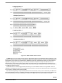
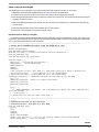
path. Figure 1 shows the simple evaluation board for the MMA745xL which is available online. This board contains the
accelerometer with all pins mapped out to a 14 pin header. The image on the left shows the ground plane which ties the digital
and analog ground pins together. This is necessary to improve the noise performance of the part based on internal trim and is
the recommendation for this part. The image in the center is the front side of the board which shows all the other connections.
This board can be wired to a Freescale MCU evaluation or demo board and programmed for various application functions which
are described in detail below.
Back View
Front View
Actual Image of the Board
Figure 1. MMA745xL Accelerometer Simple Evaluation Board
APPLICATIONS AND SENSING CAPABILITIES OF THE MMA745XL
The MMA745xL is the first family of digital 3-axis consumer accelerometers that Freescale has designed. There are several
sensing functions that accelerometers are capable of detecting. These are motion, freefall, shock, vibration, and tilt. The
advantage of a digital accelerometer is that the A/D converter is implemented within the sensor and an MCU can be used to
accompany the sensor that does not require the A/D converter. The sensor can connect directly to the SPI or IIC into the MCU.
The disadvantage is that there are selected digital filters within the sensor which limits the sampling rate for certain applications.
Motion Detection
Typically motion detection is used to identify if an object is in use or not based on change in acceleration output. The purpose
of power cycling is to try to minimize the power consumption for the application. By moving into a standby (low power) mode when
the device is not in use then switching to measurement mode (active mode) which is a full power mode, the overall power
consumption can be decreased. The power consumption is the same regardless of the two sampling rate options in the active
modes. The MMA745xL can be put into standby mode for a set period of time consuming only 5 µA. Then the device must be
programmed to switch over to measurement mode to monitor the X, Y, Z outputs to determine if a significant change in
acceleration has occurred. This can be done using a timer function in the MCU. The device will not auto wake from standby mode.
When in an active mode the device consumes 400 - 450 µA of current. The device can be power cycled between standby mode
and measurement mode minimizing the overall current consumption for the application. This is useful in a wide variety of
applications. It is particularly important in handheld devices which require batteries to operate.
© Freescale Semiconductor, Inc., 2008. All rights reserved.
Hints for a Power Cycling Algorithm
During a power cycling routine the device will be set to standby mode until the MCU timer triggers. Then the MCU will switch
the sensor into measurement mode and take one reading from X, Y and Z. If the RMS value is a certain threshold greater than
1 g or less than 1 g then motion is detected and the device will stay in measurement mode. Otherwise the MCU will switch
accelerometer back into standby mode. The timing will be somewhat dependant on the circumstances of the application and the
tradeoff between the reaction time vs. the consumed current.
Motion Detection using the MMA745xL Logic Interrupts
The Level Detection mode can be used to detect motion with an interrupt. The threshold level can be set and the interrupt will
occur when a motion greater than the threshold occurs. There are no timers in the Level Detection mode and false readings are
possible. It is recommended to set the threshold level to 2 g or greater for motion detection using the Level Detection to minimize
false readings. The Pulse Detection mode can detect motion as a single pulse or as a double pulse. The threshold and the time
of the pulse must be set. In pulse mode the detection occurs when X or Y or Z is greater than the set threshold within the set
time window (less than the time window). It is not able to detect motion for a time period greater than a set time window. Motion
detection can also be done in measurement mode sampling the X, Y and Z outputs with a set timer. This method would require
programming the algorithm with the MCU. This last method would be necessary to detect a motion for greater than a set time
period.
Freefall
Freefall is a sensing function that can be used to identify that a large impact is highly probable. This is useful in notebook
computers to park the drive heads before impact. This is useful in general for many types of electronic equipment to shut down
before impact. Freefall can also be used for warranty protection along with shock to identify how high an object has fallen to
determine the approximate resultant force. For a robust algorithm there are various different freefall conditions that should be
considered. These are linear freefall, projectile fall and rotational fall. Cheaper freefall solutions typically only consider linear
freefall.
Linear Freefall using the MMA745xL Logic Interrupts
The MMA745xL has internal logic to detect linear freefall using either the Level detection or the Pulse Detection modes. The
level detection is not as robust because it does not have any timers associated with it. It simply detects any resultant output of
X&&Y&&Z < Set Threshold. The pulse detection Freefall condition is more robust because it has a timer. The pulse detection
freefall algorithm looks at X&&Y&&Z < Threshold for > Latency Timer. The timer in the pulse detection helps avoid false readings.
Advanced Freefall Algorithm Hint
Using a microcontroller to store some of the past history and to analyze the outputs linear, projectile and rotational falls can
be detected using the MMA745xL to detect if any of these different conditions are occurring.
Shock
Shock is a sensing function of the accelerometer that is useful for warranty protection, shipping and handling and to detect the
end of a fall condition. It is also used to detect tapping. Shock is a sensing function that can be difficult to detect with the consumer
low-g accelerometers because shocks are typically high accelerations. The MMA745xL is capable of detecting up to 8g of
acceleration. In some cases freefall can be used to determine the height of a fall using the standard Newtonian equations of
motion and then back calculating for the distance.
Detecting Shock using the MMA745xL Logic Interrupts
The Level Detection interrupt can be used to detect shock in the same manner it is done for motion detection. The single and
double pulse interrupts are the most useful for shock.
Vibration
Vibration sensing is limited by the digital filtering in the accelerometer. The MMA745xL has a maximum sampling rate of
250 Hz. Therefore it is capable of detecting from DC to 125 Hz of vibration. The MMA745xL is suitable for these lower
frequencies.
AN3468
Sensors
Freescale Semiconductor
2
Tilt
Tilt is used for a lot of different applications. The cell phone and PMP market has exploded with opportunities for
accelerometers to perform tilt functions. The most popular features are portrait/landscape orientation detection, scrolling, and
menu selection. The two main challenges of tilt are to determine the required resolution and the required accuracy for the
application. The MMA745xL has a maximum sensitivity of 64 counts/g. The resolution is the smallest detectable change in
acceleration which is 16 mg per count. This corresponds to about 1.5 degrees of resolution using two axes. The accuracy is how
closely the true value is equal to the measured value from the accelerometer. This is dependant on the sum of all errors from the
accelerometer. Typically after calibration the accuracy is about ±4 degrees.
SENSOR PLACEMENT
Sensor placement is very important and is often overlooked. The MEMS sensor inside the package is very sensitive to
stresses. Small deflections inside the MEMS sensor on the order of 10 nm correspond to a change in acceleration of 1 g. Care
must be taken to ensure that the package is not stressed by holes or components on the PCB placed too closely to the
accelerometer. Please review the mounting guidelines in AN3484. It is important to not place the sensor near an edge where it
may be knocked around or touched by people’s hands. Also avoid bending the PCB as the PCB stress is transferred to the
accelerometer. Temperature can also be an issue. It is good to avoid placing the sensor far away from components that may have
large temperature variations, or that are constantly very hot as this will also affect the offset of the sensor. For optimal motion
detection, place the sensor away from the center of the device. This will ensure better acceleration readings and make them more
significant to detect smaller motions, from a higher moment of inertia than if placed right on the center of movement.
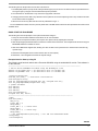
Connecting the MMA745xL to an MCU using I2C Communication
Connecting this evaluation board to an MCU using I2C communication is simple. Connect power and ground, SDA and the
SCL lines appropriately to the MCU.
Figure 2. I2C Communication Sensor Connections
AN3468
Sensors
Freescale Semiconductor
3
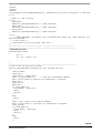
Figure 3. IIC Read and Write Protocol Format
The MMA745XL IIC communication protocol follows the Philips Semiconductors (now NXP Semiconductors) standard. In this
interface only two bus lines are required: a serial data line (SDA) and a serial clock line (SCL). Serial, 8-bit oriented bidirectional
data transfers can be made at up to 100 kbit/s in the Standard-mode and up to 400 kbit/s in the fast-mode. These modes are
adjustable by changing the clock frequency. The maximum allowable bus capacitance is 400pF. Both SDA and SCL are
bidirectional lines, connected to a positive supply voltage via a pull-up resistor. The recommended value is between 2.2 kΩ –
4.7 kΩ. The accelerometer is always considered the slave and the MCU is always considered the master. The accelerometer is
not capable of stretching the clock.
The benefits of the I2C Communication interface is that many ICs can be added to this bus. The only limitation is the bus
capacitance. The simple 2-wire serial I2C-bus minimizes interconnections so ICs have fewer pins and there are not as many PCB
traces, resulting in smaller and less expensive PCBs.
Each device is recognized by a unique address (whether it is a microcontroller, memory or an accelerometer). The MMA7455L
has an extra address bit to allow for two different addresses available but the address pin on this sensor has been disabled. This
device is addressed by $1D only. The IADDR0 pin is enabled on the MMA7458L, which will be available in Q4 2008.
AN3468
Sensors
Freescale Semiconductor
4
The following are four simple rules of the IIC bus to be aware of:
1. The SDA (data) and SCL (clock) cannot actively be driven high by any I2C device. I2C devices must use open-drain drivers.
The logic is high by using the recommended external pull-up resistors.
2. The information on the data line is only read on the high phase of the clock.
3. Changing the level of the data is only allowed in the low phase of the clock except during start or stop conditions and this
is how these events are signified.
4. When the bus is not busy SDA and SCL lines are pulled back to logic “1”.
For more detailed information on the IIC protocol please refer to the NXP Semiconductor IIC bus specification and user manual
available online.
BASIC START-UP PROCEDURE
The following are some simple steps to set up the accelerometer using IIC.
1. Set up the microcontroller hardware shown above for IIC communication.
2. Configure the clock speed and all the pins required. The speed is set by adjusting the baud rate.
3. Write simple single byte Read and Write command to communicate to the device. The example below was done using the
MC9S08QE hardware controller for the IIC.
4. Write to the MMA745xL Register $16, sending in a value of 0x05 to set up the device for measurement mode with ±2g
dynamic range.
5. Read the Control Register $16 to ensure that the value is correct (0x05).
6. Read the X, Y and Z registers and watch the outputs change.
Example Code for Start-up using IIC
The following code has been written with a Freescale S08 MCU using the embedded IIC module. This software is
for the host side.
//--------------------------------------------------------------------------------// HW I2C driver embedded I2C module using FSL MC9S08QE K. Tuck
#define IIC_WriteAdr 0x1D // $1D shifted in with a 0 had been $3A
#define IIC_ReadAdr 0x1D // $1D shifted in with a 1 had been $3B
//Function Definitions
void MCU_init(void); // From Device initialization
void Delay(byte count);
void IIC_SingleByteWrite(unsigned char reg, unsigned char val);
char IIC_SingleByteRead(unsigned char reg);
// global variables
char Xdata=0;
char Ydata=0;
char Zdata=0;
char ControlRegVal=0;
unsigned char ACK, write1;
//-----------------------------------------------------------------------//Main
void main(void) {
MCU_init();
IIC2C1_MST = 0;
Delay(0xFF);
IIC2C1_MST = 1; // create start
Delay(0xFF);
IIC2C1_MST = 0; // create stop
Delay(0xFF);
/ //IIC_SingleByteWrite(0x16,0x05); // Put ION into Measurement Mode
Delay(0xFF);
ControlRegVal=0;
AN3468
Sensors
Freescale Semiconductor
5
Xdata=0;
Ydata=0;
Zdata=0;
ControlRegVal= IIC_SingleByteRead(0x16); //Read back out the value of Register 16, make sure
it is 5
// Read X, Y, and Z forever
for(;;) {
Delay(0xFF);
Xdata=IIC_SingleByteRead(0x06); // Read X Register
Delay(0xFF);
Ydata=IIC_SingleByteRead(0x07); // Read Y Register
Delay(0xFF);
Zdata=IIC_SingleByteRead(0x08); // Read Z Register
}
for(;;) {
/* __RESET_WATCHDOG(); by default, COP is disabled with device init. When enabling, also
reset the watchdog. */
} /* loop forever */
/* please make sure that you never leave main */
}
//------------------------------------------------------------------------//------------------------------------------------------------------------//Simple Delay Function
void Delay(byte count)
{
byte i;
for (i=0; i<count; i++)
{
}
}
//--------------------------------------------------------------------------// This is the I2C byte write function
void IIC_SingleByteWrite(unsigned char reg, unsigned char val)
{
IIC2C1_IICEN=1;
IIC2C1_TX=1;
IIC2C1_MST=1; //Sends Start;
IIC2D = (IIC_WriteAdr<<1);
// send the accelerometer address
while (IIC2S_IICIF==0);//Waiting for transmission to complete
Delay(100);
IIC2S_IICIF=1;
Delay(100);
if (IIC2S_RXAK==1){
IIC2C_MST=0; //send stop
ACK=0;
while(1);
}
else{
ACK=1;
}
IIC2D = reg; //write in the register address
while (IIC2S_IICIF==0 );//Waiting for transmission to complete
IIC2S_IICIF=1;
if (IIC2S_RXAK==1){
IIC2C1_MST=0; //send stop
ACK=0;
while(1);
}
else{
ACK=1;
}
AN3468
Sensors
Freescale Semiconductor
6
IIC2D = val;
// send the data to be written
while (IIC2S_IICIF==0);//Waiting for transmission to complete
IIC2S_IICIF=1;
if (IIC2S_RXAK==1){
IIC2C_MST=0; //send stop
ACK=0;
while(1);
}
else{
ACK=1;
}
IIC2C1_MST=0;
write1=1;
}
//-----------------------------------------------------------------------------//-----------------------------------------------------------------------------// This is the I2C byte read function
char IIC_SingleByteRead(unsigned char reg)
{
char data;
IIC2C1_IICEN=1;
IIC2C1_TX=1;
IIC2C1_MST=1; //Sends Start;
IIC2D = (IIC_WriteAdr<<1);
// send the accelerometer address
Delay(0x50);
while (IIC2S_IICIF==0);//Waiting for transmission to complete
IIC2S_IICIF=1;
if (IIC2S_RXAK==1){
IIC2C_MST=0; //send stop
ACK=0;
while(1);
}
else{
ACK=1;
}
IIC2D = reg; //write in the register address
Delay(0x50);
//Check_ACK(); //check ACK
while (IIC2S_IICIF==0);//Waiting for transmission to complete
IIC2S_IICIF=1;
if (IIC2S_RXAK==1){
IIC2C_MST=0; //send stop
ACK=0;
while(1);
}
else{
ACK=1;
}
//Sending a Restart, the device Address with a Read
IIC2C1_TX=1;
IIC2C1_RSTA=1; //Sends Start;
IIC2D =(IIC_ReadAdr<<1)|0x01;
// Send the accelerometer device address with the Read Bit
//Delay(100);
//Check_ACK(); //check ACK
while (IIC2S_IICIF==0);//Waiting for transmission to complete
IIC2S_IICIF=1;
if (IIC2S_RXAK==1)
{
IIC2C_MST=0; //send stop
ACK=0;
while(1);
AN3468
Sensors
Freescale Semiconductor
7
}
else{
ACK=1;
}
IIC2C1_TX=0; // Change over to Receiver Mode
IIC2C_TXAK = 1;
// send NACK in the next read
data=IIC2D;
//dummy read
while (IIC2S_IICIF==0);
IIC2S_IICIF=1;
// wait until the transmission ends
data = IIC2D;
//This is the real Read command
while (IIC2S_IICIF==0);
// wait until the transmission ends
IIC2S_IICIF=1;
//Clear the interrupt flag
IIC2C1_MST = 0;
// send a stop, leave master mode
return(data);
}
//---------------------------------------------------------------------------
General Pseudo Code using IIC
The following is general IIC code based on work by V.Himpe1.
n,x = general BYTE
SIZE = max number
DATA(SIZE) = an array holding up to SIZE number of bytes. This will contain the data transmitted and store received data.
BUFFER = a byte value holding immediate received or transmit data.
/ $$$$$$$$$$$$$$$$$$$$$$$$$$$$$$$$$$$$$$$$$$$$$$$$$$$$$$$$$$$$$$$$$$$$$$$ / / **** I2C Driver
General I2C Pseudo Code Released as Public Domain **** / /
$$$$$$$$$$$$$$$$$$$$$$$$$$$$$$$$$$$$$$$$$$$$$$$$$$$$$$$$$$$$$$$$$$$$$$$ /
DECLARE N,SIZE,BUFFER,X Byte
DECLARE DATA() Array of SIZE elements
SUBroutine I2C_INIT / call this immediately after power-on /
SDA=1
SCK=0
FOR n = 0 to 3
CALL STOP
NEXT n
ENDsub
SUBroutine START
SCK=1
SDA=1
SDA=0
SCK=0
SDA=1
ENDsub
SUBroutine STOP
SDA=0
SCK=1
SDA=1
ENDsub
SUBroutine PUTBYTE(BUFFER)
FOR n = 7 TO 0
SDA= BIT(n) of BUFFER
SCK=1
SCK=0
NEXT n
SDA=1
ENDsub
SUBroutine GETBYTE
FOR n = 7 to 0
1. http://www.esacademy.com/faq/i2c/general/i2cpseud.htm
AN3468
Sensors
Freescale Semiconductor
8
SCK=1
BIT(n) OF BUFFER = SDA
SCK=0
NEXT n
SDA=1
ENDsub
SUBroutine GIVEACK
SDA=0
SCK=1
SCK=0
SDA=1
ENDsub
SUBroutine GETACK
SDA=1
SCK=1
WAITFOR SDA=0
SCK=0
ENDSUB
/ this concludes the low-level set of instructions for the I2C driver
The next functions will handle the telegram formatting on a higher level /
SUBroutine READ(Device_address,Number_of_bytes)
Device_adress=Device_adress OR (0000.0001)b /This sets the READ FLAG/
CALL START
CALL PUTBYTE(Device_adress)
CALL GETACK
FOR x = 0 to Number_of_bytes
CALL GETBYTE DATA(x)=BUFFER /Copy received BYTE to DATA array /
IF X< Number_of_bytes THEN /Not ack the last byte/
CALL GIVEACK
END IF
NEXT x
CALL STOP
ENDsub
SUBroutine WRITE(Device_address,Number_of_bytes)
Device_adress=Device_adress AND (1111.1110)b / This clears READ flag /
CALL START
CALL PUTBYTE(Device_adress)
CALL GETACK
FOR x = 0 to Number_of_bytes
CALL PUTBYTE (DATA(x))
CALL GETACK
NEXT x
CALL STOP
ENDsub
SUBroutine RANDOMREAD(Device_adress,Start_adress,Number_of_bytes)
Device_adress=Device_adress AND (1111.1110)b / This clears READ flag /
CALL START
CALL PUTBYTE(Device_adress)
CALL GETACK
CALL PUTBYTE(Start_adress)
CALL GETACK
CALL START /create a repeated start condition/
Device_adress=Device_adress OR (0000.0001)b /This sets the READ FLAG/
CALL PUTBYTE(Device_adress)
CALL GETACK
FOR x = 0 to Number_of_bytes
CALL GETBYTE
DATA(x)=BUFFER
CALL GIVEACK
NEXT x
CALL STOP
ENDsub
AN3468
Sensors
Freescale Semiconductor
9
For further information and examples using the QE128 Freescale S08 with the MMA745xL there is an example with a SW
implementation of the driver available in the following software application notes on-line.
• AN3479SW: shows the programming required to communicate to the device using the IIC bus.
• AN3468SW: has examples of using measurement mode, level mode and pulse detection.
• AN3571SW: shows different settings for using either the level or the pulse detection mode
Connecting the MMA745xL to an MCU using SPI Communication
When connecting the sensor to the MCU using SPI communications there are 6 connections into the MCU. These connections
are power, ground, the clock (SPSCK), MOSI (data), MISO (data) and CS which is the slave select line.
Figure 4. SPI Communication Sensor Connections
AN3468
Sensors
Freescale Semiconductor
10
Figure 5. SPI Timing Diagrams
SPI communication can be implemented using 4 lines: MOSI (master-output/slave-input), MISO (master-input/slave-output),
SS (slave select), and SPSCK (SPI serial clock). The master device initiates all SPI data transfers. During a transfer, the master
shifts data out (on the MOSI pin) to the slave while simultaneously shifting data in on the MISO pin from the slave (SDO). The
transfer effectively exchanges the data that was in the SPI shift registers of the two SPI systems. The SPSCK signal is a clock
output from the master and an input to the slave. The slave device must be selected by a low level on the slave select input (CS
pin). The MMA745xL is in SPI 4 wire mode by default. Register $16 contains a bit labeled SPI3W, which is set to 0 by default for
4 wire mode. SPI communication can also be implemented using 3 lines: MIMO (master-in/master-out), SS(slave select), SPSCK
(SPI serial clock). The SDA/I/O line on the MMA745xL changes from being an input into the accelerometer and becomes a
bidirectional line. To set up the sensor for 3 wire SPI communication bit SPI3W in Register $16 (Control Register 1) must be set
to 1. For four wire SPI mode SPI3W is set to 0. The following example shows how to set up the register in either mode and into
2 g measurement mode.
WriteRegister (0x16, 0x25) to set the accelerometer into SPI 3 wire mode 2 g measurement mode.
WriteRegister (0x15, 0x05) to set the accelerometer into SPI 4 wire mode 2 g measurement mode.
When using the SPI bus the register value is sent with the first value being a 1 to indicate write or 0 to indicate a read command.
Note this is opposite from the IIC R/W bit. The address is 6 bits, followed by a “Don’t Care” bit, which has no meaning to the slave.
For example to send a read command the six bit register data is simply shifted left 1 bit. (SPI2D= ((reg &0x3F)<<1);). For a write
command the first bit is a 1. SPI2D=(((reg &0x3F)<<1)|0x80);
The SPI clock speed of the sensor can go up to 4 MHz which is configured by the baud rate chosen in the MCU. This is the
maximum achievable speed when DVdd is less than 2.4 V. When DVdd is greater than 2.4 V up to 8 MHz is achievable.
AN3468
Sensors
Freescale Semiconductor
11
BASIC START-UP PROCEDURE
The following are some simple steps to set up the accelerometer with an MCU for the SPI communication.
1. Set-up the microcontroller hardware shown in Figure 4 for SPI communication.
2. Configure the clock speed and all the pins required. The speed is set by adjusting the baud rate.
3. Write simple single byte Read and Write command to communicate to the device. The example below was done using the
hardware controller for the SPI.
4. Write to the MMA745xL Register $16, sending in a value of 0x05 to set up the device for measurement mode with ±2g
dynamic range.
5. Read the Control Register $16 to ensure that the value is correct (0x05).
6. Read the X, Y and Z registers and watch the outputs change.
Example Code for Start-up using SPI
The following example code was developed with a Freescale S08 MCU using the embedded SPI module. This software is for
the host side. This example shows the code for both 4Wire Mode and 3Wire Mode. The MCU can be initialized for 3-Wire Mode
or for 4-Wire Mode and the following code will execute.
//--------------------------------------------------------------------------------// HW SPI driver embedded SPI module using FSL S08QE MCU K. Tuck
//--------------------------------------------------------------#define CS PTDD_PTDD3
byte Xdata,Ydata,Zdata,CTLReg;
void MCU_init(void); /* Device initialization function declaration */
byte spi_read(byte reg);
void spi_write(byte reg, byte data);
void main(void) {
MCU_init(); /* call Device Initialization */
PTDD_PTDD3=1; //CS Pin description
PTDDD_PTDDD3=1;
Xdata=0;
CTLReg=0;
//Set up sensor for SPI 3 Wire Mode or 4 Wire Mode by writing to SPI3W in Register $16
spi_write(0x16,0x25);
//3 Wire Mode Set up in the Accelerometer
// spi_write(0x16,0x05); //4 Wire Mode Set up in the Accelerometer
CTLReg=spi_read(0x16); // Read back the value that has been set for the Mode
for (;;){
Xdata=spi_read(0x06); //Read X,Y,Z outputs from Sensor
Ydata=spi_read(0x07);
Zdata=spi_read(0x08);
}
for(;;) {
/* __RESET_WATCHDOG(); by default, COP is disabled with device init. When enabling, also
reset the watchdog. */
} /* loop forever */
/* please make sure that you never leave main */
}
//--------------------------------------------------------------------------------------------------// Function Definitions for Read and Write
// Read function SPI 3 Wire Mode or 4 Wire Mode
byte spi_read(byte reg){
byte x;
CS=0;
x=SPI2S;
x=SPI2D;
while (!SPI2S_SPTEF);
SPI2D= ((reg &0x3F)<<1); // write in the register address with the read command
while(!SPI2S_SPRF); //wait for transfer
AN3468
Sensors
Freescale Semiconductor
12
x=SPI2D;
SPI2C2_BIDIROE = 0;
// MOSI become input when 3 wire mode
SPI2D = 0x00;
// send 2nd byte
while (!SPI2S_SPRF);
// wait transfer done
x = SPI2D;
SPI2C2_BIDIROE = 1;
//change direction back to output when in 3 wire mode
CS=1;
return (x);
}
//--------------------------------------------------------------------------------------------------//Write function SPI 3 Wire or SPI 4 Wire Mode
void spi_write(byte reg, byte data){
byte x;
CS=0;
SPI2D=(((reg &0x3F)<<1)|0x80);
while (!SPI2S_SPRF); //wait for transmission complete
x=SPI2D; //dummy read
SPI2D=data;
while (!SPI2S_SPRF); //wait for transmission complete
x=SPI2D;
CS=1;
}
//------------------------------------------------------------------------------------------------------
General Pseudo Code using SPI
This is pseudo code for general communication.
1. SS = 0 Slave Select is cleared
2. Assert MOSI most significant bit
3. Toggle the clock
4. Shift the next data bit onto the MOSI pin
5. Repeat 3 and 4 until done
6. SS = 1 Slave Select is set
For further examples using the SPI SW protocol please refer to
• AN3468SW: has examples of using measurement mode, level mode and pulse detection.
• AN3480SW: shows the programming required to communicate to the device using the SPI bus.
• AN3571SW: shows different settings for using either the level or the pulse detection mode
AN3468
Sensors
Freescale Semiconductor
13
PROGRAMMING THE MMA745XL
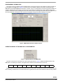
This section focuses on explaining all the available features of the device which are all accessible by reading and writing to
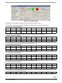
the 32 registers of the MMA745xL. Figure 6 is a screen shot of an evaluation interface for this device. This GUI uses the
MMA745xL with the MC9S08QG8 microcontroller on a small 1 inch by 1 inch board which connects through SCI to USB to the
computer. It displays the 3-axis output on a scope screen to view motion of the different axes. All the different settings and
operation modes of the device are displayed on the menu buttons or sliders. On the right hand side all the useful registers of the
device are displayed. This allows the user to view how the registers change when different settings are changed.
Figure 6. MMA745XL Evaluation Software Interface
OPERATION MODES OF THE MMA745XL ACCELEROMETER
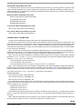
Figure 7. Operation Modes of the MMA745XL
All modes of the device are controlled in the mode control register (MCTL). Figure 7 displays the different modes of the
MMA745XL. The following are the bits in the register and the different modes that the device can be set.
$16
MCTL
LPEN
DRPD
SPI3W
STON
GLVL[1]
GLVL[0]
MOD[1]
MOD[0]
Standby mode is a low power mode consuming less than 5 µA. This mode is used when the sensor is not needed to take new
data. In standby mode the sensor can read and write to the registers and the other sensor detection modes are easily enabled.
AN3468
Sensors
Freescale Semiconductor
14
Standby Mode: RegisterWrite (0x16, 0x00)
In measurement mode the device can be set up for 3 different dynamic ranges (2 g, 4 g and 8 g). With the 8 g dynamic range
8-bit or 10-bit data is available. The 2 g and 4 g ranges are only 8-bit data. The 10-bit data is available by reading X: $00-01,
Y$02-03 and Z$04-05. In 2 g mode and 4 g mode the ten bit data will match the 8-bit data. In 8 g mode the 10-bit data is going
to be 4 times that of the 8-bit data.
Measurement Mode: RegisterWrite (0x16,0x01)
Dynamic Range Settings: In Measurement Mode
2g: RegisterWrite(0x16, 0x05)
4g RegisterWrite (0x16,0x09)
8g RegisterWrite (0x16,0x01)
Level Detection Mode: RegisterWrite (0x16, 0x02)
*Note: Dynamic range setting is automatically 8 g
Pulse Detection Mode: RegisterWrite (0x16, 0x03)
*Note: Dynamic range setting is automatically 8 g
CALIBRATION OF THE MMA745XL
The offset can be calibrated by storing the offset values in the designated offset drift registers
$10 to $15 in the accelerometer. These values will be stored until the part loses power and therefore it is a good idea to store
these values in the memory of a microcontroller, used in conjunction with the sensor. This will provide automatic calibration of the
sensor each time the sensor is turned back on. In order to calibrate the MMA745xL 0g offset, the predetermined digital offset
values should be subtracted from the reading of the actual digital sensing values. The following procedure is a recommendation
for how this can be accomplished:
Step 1. After power up, set up the “Mode Control Register”(Register $16) to be in “measurement mode” by writing $05 into
Register $16. Then read the X, Y and Z offset values from the Registers $00-$08. The first 6 registers of the 9 are 10-bit XYZ
output values: LSB, first; MSB, second. Please verify with the data sheet for detailed register information.
Step 2. In this step, the offset compensation is calculated to shift the offset to zero. For example, if the 0g offset is calibrated
flat (where X = 0 g, Y = 0 g and Z = +1 g) in 2 g mode (64 LSB/g sensitivity), the outputs from Registers $00-$08 might be the
following: X = +18,Y = -20, Z = +44. In this case,
• X must be shifted by -18 to get X back to zero
• Y must be shifted by +20 to get to zero
• Z must be shifted by (+64-44) = +20 to get to +64 (since Z is in the +1 g orientation)
Step 3. These compensation values can be written in hexadecimal into the “Offset Drift Registers” $10-$15.The Offset Drift
Registers require each value to be½ LSB, therefore the calibration values calculated in Step 2 must be multiplied by two. Note
that there will still be a bit of offset shift, and you may need to multiply by a bit more than two to exactly subtract the offset.
If the register values in the X = 0 g, Y = 0 g and Z = +1 g orientation are the following:
X=+18, Y=-20, Z=+44
Write -36 (DC Hex) into the X drift Register $10
Write +40 (28 Hex) into the Y drift Register $12
Write +40 (28 Hex) into the Z drift Register, $14
If the compensation requires negative values, remember that 2’s complement is always used in hexadecimal for storing the
signed value as was done for the X axis above. If using 10-bit mode, and the calibrated values are greater than 8 bits, then there
is another register for up to 3 more bits:
• Register $10 and $11 are for X
• Register $12 and $13 are for Y
• Register $14 and $15 are for Z
These registers follow signed byte data using 2’s complement. Reading or writing low byte (X, Y or Z) OUTL latches high byte
data (X, Y, or Z) OUTH to allow coherent 10-bit reads or writes. (X, Y, or Z) OUTH should be read/written directly following (X, Y
or Z) OUTL.
Step 4. After this compensation process is complete, you can continue to modify the values by overcompensating until you get
the final output to be right at 0 for X and Y and at 64 for Z. Note this is an iterative process.
AN3468
Sensors
Freescale Semiconductor
15
Step 5. Now the calibrated values are stored in the “Offset Drift Registers”. To avoid the values being erased when the power
is turned off, it is recommended to store these values in flash or a nonvolatile memory in the main processor or external to the
processor. It is also recommended to include a short start-up sequence to write the compensation values stored in flash or
nonvolatile memory to the registers $10-$15 in the accelerometer on start-up. If a microcontroller is used, a recursive program is
available to auto-calibrate the device.
To set the 0 g offset the following recursive program can be written as a routine in the software.
Place the part flat in the x = 0 g,y = 0 g, z = 1 g orientation:
1. Set the Accelerometer in measurement Mode: 2g
RegisterWrite (0x16,0x01)
2. Initialize the X Y and Z calibration variables to 0.
Xcal=0;
Ycal=0;
Zcal=0;
3. Read X, Y and Z data
Xdata=RegisterRead (0x00);
While (Xdata>1 || Xdata<-1){
Xcal += -2*Xdata;
Delay (0xFF);
Xdata=RegisterRead(0x00);
}
Ydata=RegisterRead (0x02);
While (Ydata>1 || Ydata<-1){
Ycal += -2*Ydata;
Delay (0xFF);
Ydata=RegisterRead(0x02);
}
Zdata=RegisterRead (0x04);
While (Zdata>65 || Zdata< 63){
If (Zdata>65){Zcal+=(Zdata-64)*2}
Else{Zcal+=(64-Zdata)*2}
Delay(0xFF);
Zdata=RegisterRead(0x04);
}
SETTING UP THE SAMPLING FREQUENCY AND SELF TEST
To set the bandwidth filter to 62.5 Hz the sampling frequency will be 125 Hz. Clear DFBW in Control Register 1.
RegisterWrite (0x18,regs[0x18] & 0xEF)
$18
CTL1
DFBW
THOPT
ZDA
YDA
XDA
INTRG[1]
INTRG[0]
INTPIN
$18
mask
0
1
1
1
1
1
1
1
$18
result
0
THOPT
ZDA
YDA
XDA
INTRG[1]
INTRG[0]
INTPIN
To set the bandwidth filter to 125 Hz the sampling frequency will be 62.5 Hz. Set DFBW in Control Register 1.
RegisterWrite (0x18,regs[0x18] | 0x80)
$18
CTL1
DFBW
THOPT
ZDA
YDA
XDA
INTRG[1]
INTRG[0]
INTPIN
$18
mask
1
0
0
0
0
0
0
0
$18
result
1
THOPT
ZDA
YDA
XDA
INTRG[1]
INTRG[0]
INTPIN
AN3468
Sensors
Freescale Semiconductor
16
To verify the self test. Set STON in Mode Control Register $16. Clear STON to turn off self test.
RegisterWrite(0x16, regs[0x16] ^ 0x10)
$16
MCTL
LPEN
DRPD
SPI3W
STON
GLVL[1]
GLVL[0]
MOD[1]
MOD[0]
$16
mask
0
0
0
1
0
0
0
0
$16
result
LPEN
DRPD
SPI3W
~STON
GLVL[1]
GLVL[0]
MOD[1]
MOD[0]
SETTING UP INT1 AND INT2 INTERRUPT REGISTERS
This section explains how to set up the interrupt pins in all possible configurations.
The interrupt registers are set up in the Control 1 (CTL1) Register to determine which interrupt is assigned to Level detection
and which is assigned to Pulse detection. Figure 6 and Figure 8 displays the different options for setting up the interrupt pins.
Figure 8. Setting up the Interrupt Registers for Level and Pulse Detection
INT1 reg= Level and INT2 reg= Pulse
RegisterWrite(0x18, regs[0x18]&0xF9)
$18
CTL1
DFBW
THOPT
ZDA
YDA
XDA
INTRG[1]
INTRG[0]
INTPIN
$18
mask
1
1
1
1
1
0
0
1
$18
result
DFBW
THOPT
ZDA
YDA
XDA
0
0
INTPIN
INT1 reg= Pulse and INT2 reg= Level
RegisterWrite(0x18,(regs[0x18]&0xFB)|0x02)
$18
CTL1
DFBW
THOPT
ZDA
YDA
XDA
INTRG[1]
INTRG[0]
INTPIN
$18
mask
1
1
1
1
1
0
1
1
$18
result
DFBW
THOPT
ZDA
YDA
XDA
0
1
INTPIN
INT1 reg= Single Pulse and INT2 reg= Pulse
RegisterWrite(0x18,(regs[0x18]&0xFD)|0x04)
$18
CTL1
DFBW
THOPT
ZDA
YDA
XDA
INTRG[1]
INTRG[0]
INTPIN
$18
mask
1
1
1
1
1
1
0
1
$18
result
DFBW
THOPT
ZDA
YDA
XDA
1
0
INTPIN
INT1pin assigned to DRDY
This pin can be set to allow INT1 to be used to indicate when data is ready from the sensor
RegisterWrite(0x16, reg[0x16]^0x40)
$16
MCTL
LPEN
DRPD
SPI3W
STON
GLVL[1]
GLVL[0]
MOD[1]
MOD[0]
$16
mask
0
1
0
0
0
0
0
0
$16
Result
LPEN
~DRPD
SPI3W
STON
GLVL[1]
GLVL[0]
MOD[1]
MOD[0]
AN3468
Sensors
Freescale Semiconductor
17
INT1pin assigned to INT1 Reg (INT2pin =INT2 Reg)
RegisterWrite(0x18, regs[0x18]&FE)
$18
CTL1
DFBW
THOPT
ZDA
YDA
XDA
INTRG[1]
INTRG[0]
INTPIN
$18
mask
1
1
1
1
1
1
1
0
$18
result
DFBW
THOPT
ZDA
YDA
XDA
INTRG[1]
INTRG[0]
0
INT1pin assigned to INT2 Reg (INT2pin = INT1 Reg)
RegisterWrite(0x18, regs[0x18] | 0x01)
$18
CTL1
DFBW
THOPT
ZDA
YDA
XDA
INTRG[1]
INTRG[0]
INTPIN
$18
mask
0
0
0
0
0
0
0
1
$18
result
DFBW
THOPT
ZDA
YDA
XDA
INTRG[1]
INTRG[0]
1
LEVEL DETECTION MODE
Level detection mode is capable of detecting both motion and freefall. There are no timers associated with the level detection.
The OR logic is used for motion detection and the AND logic is used for freefall detection. Then there is signed threshold detection
(+ or -) or absolute (+ and -).
Figure 9. Level Detection Settings
These are the following available options for Level Detection Mode and how they can be enabled.
For motion or for freefall detection there is an absolute condition that can be used.
RegisterWrite(0x18,regs[0x18]&0xBF)
$18
CTL1
DFBW
THOPT
ZDA
YDA
XDA
INTRG[1]
INTRG[0]
INTPIN
$18
mask
1
0
1
1
1
1
1
1
$18
result
DFBW
0
ZDA
YDA
XDA
INTRG[1]
INTRG[0]
INTPIN
For motion detection there is a positive/negative detection condition that can be used.
RegisterWrite (0x18,regs[0x18]|0x40)
$18
CTL1
DFBW
THOPT
ZDA
YDA
XDA
INTRG[1]
INTRG[0]
INTPIN
$18
mask
0
1
0
0
0
0
0
0
$18
result
DFBW
1
ZDA
YDA
XDA
INTRG[1]
INTRG[0]
INTPIN
AN3468
Sensors
Freescale Semiconductor
18
For motion detection only there is an or logic condition that can be used. LDPL=0
RegisterWrite (0x19,regs[0x19]&0xFE)
$19
CTL2
--
--
--
--
--
DRVO
PDPL
LDPL
$19
mask
1
1
1
1
1
1
1
0
$19
Result
--
--
--
--
--
DRVO
PDPL
0
For freefall detection only there is an and logic condition that can be used. LDPL=1
RegisterWrite1(0x19,regs[0x19]|0x01)
$19
CTL2
--
--
--
--
--
DRVO
PDPL
LDPL
$19
mask
0
0
0
0
0
0
0
1
$19
result
--
--
--
--
--
DRVO
PDPL
1
This is an example of how to toggle the XDA bit to enable or disable the X-axis.
RegisterWrite1(0x18,regs[0x18]^0x08)
$18
CTL1
DFBW
THOPT
ZDA
YDA
XDA
INTRG[1]
INTRG[0]
INTPIN
$18
mask
0
0
0
0
1
0
0
0
$18
result
DFBW
THOPT
ZDA
YDA
~XDA
INTRG[1]
INTRG[0]
INTPIN
This is an example of how to toggle the YDA bit to enable or disable the Y-axis.
RegisterWrite1(0x18,regs[0x18]^0x10)
$18
CTL1
DFBW
THOPT
ZDA
YDA
XDA
INTRG[1]
INTRG[0]
INTPIN
$18
mask
0
0
0
1
0
0
0
0
$18
result
DFBW
THOPT
ZDA
~YDA
XDA
INTRG[1]
INTRG[0]
INTPIN
XDA
INTRG[1]
INTRG[0]
INTPIN
This is an example of how to toggle the ZDA bit to enable or disable the Z-axis.
RegisterWrite1(0x18,regs[0x18]^0x20)
$18
CTL1
DFBW
THOPT
ZDA
YDA
$18
mask
0
0
1
0
0
0
0
0
$18
result
DFBW
THOPT
~ZDA
YDA
XDA
INTRG[1]
INTRG[0]
INTPIN
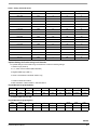
This is the register for setting the threshold value. In Threshold Detection Mode the sensitivity is 16 counts/g. The threshold is
set in the LDTH $1A 8-bit Register.1 shows the hex values with the associated counts and g-values to understand how to program
in the level value that corresponds to the acceleration threshold desired.
$1A
LDTH
LDTH[7]
LDTH[6]
LDTH[5]
LDTH[4]
LDTH[3]
LDTH[2]
LDTH[1]
LDTH[0]
In Threshold Detection Mode the sensitivity is 16 counts/g. The threshold is set in the LDTH $1A 8-bit Register.
AN3468
Sensors
Freescale Semiconductor
19
Table 1. Setting Threshold Values
Binary
Hex
Decimal
Counts
g-value
0000 0000
0x00
0
0
0g
0001 0000
0x10
16
16
1g
0010 0000
0x20
32
32
2g
0011 0000
0x30
48
48
3g
0100 0000
0x40
64
64
4g
0101 0000
0x50
80
80
5g
0110 0000
0x60
96
96
6g
0111 0000
0x70
112
112
7g
0111 1111
0x7F
127
127
8g
1000 0000
0x80
-128
128
-8g
1001 0000
0x90
-112
144
-7g
1010 0000
0xA0
-96
160
-6g
1011 0000
0xB0
-80
176
-5g
1100 0000
0xC0
-64
192
-4g
1101 0000
0xD0
-48
208
-3g
1110 0000
0xE0
-32
224
-2g
1111 0000
0xF0
-16
240
-1g
1111 1111
0xFF
-1
255
0g
Optimal Settings for Freefall using Level Detection
For optimal settings for the freefall using Level Detection choose the following settings:
1. Absolute Logic (THOPT)
2. X, Y, and Z must be enabled (ZDA,YDA,XDA)
3. Negative AND Logic (LDPL=1)
4. LDTH: Level Detection Threshold =0x03=0.19g
1. THOPT=0 Absolute Condition
2. ZDA=0 Enable Z, YDA=0 Enable Y, XDA=0 Enable X
RegisterWrite(0x18,regs[0x18]&0x87)
$18
CTL1
DFBW
THOPT
ZDA
YDA
XDA
INTRG[1]
INTRG[0]
INTPIN
$18
mask
1
0
0
0
0
1
1
1
$18
result
DFBW
0
ZDA
YDA
XDA
INTRG[1]
INTRG[0]
INTPIN
--
--
--
--
DRVO
PDPL
LDPL
3. Negative AND Logia Set LDPL
RegisterWrite(0x19,regs[0x19]|0x01)
$19
CTL2
--
$19
mask
0
0
0
0
0
0
0
1
$19
Result
--
--
--
--
--
DRVO
PDPL
1
AN3468
Sensors
Freescale Semiconductor
20
4. Set Threshold = 0.19 g
RegisterWrite(0x1A,0x03)
$1A
LDTH
LDTH[7]
LDTH[6]
LDTH[5]
LDTH[4]
LDTH[3]
LDTH[2]
LDTH[1]
LDTH[0]
Set the threshold to 3 counts (3/16 = 0.1875 g)
Optimal Settings for Motion using Level Detection
For optimal settings for the motion using Level Detection choose the following settings:
1. Absolute Logic (THOPT)
2. X, Y enabled (YDA,XDA) with Z disabled
3. Positive OR Logic (LDPL=0)
4. LDTH: Level Detection Threshold =0x20 (2 g)
1. THOPT=0 Absolute Condition
2. ZDA=1 Disable Z, YDA=0 Enable Y, XDA=0 Enable X
RegisterWrite(0x18,((regs[0x18]&0x87) | 0x20)
$18
CTL1
DFBW
THOPT
ZDA
YDA
XDA
INTRG[1]
INTRG[0]
INTPIN
$18
mask
1
0
1
0
0
1
1
1
$18
result
DFBW
0
ZDA
YDA
XDA
INTRG[1]
INTRG[0]
INTPIN
--
--
--
--
DRVO
PDPL
LDPL
3. Positive OR Logic Clear LDPL
RegisterWrite(0x19,regs[0x19]&0xFE)
$19
CTL2
--
$19
mask
1
1
1
1
1
1
1
0
$19
result
--
--
--
--
--
DRVO
PDPL
0
LDTH[7]
LDTH[6]
LDTH[5]
LDTH[4]
LDTH[3]
LDTH[2]
LDTH[1]
LDTH[0]
4. Set Threshold to 2 g
RegisterWrite(0x1A,0x20)
$1A
LDTH
Set the threshold to 32 counts (32/16 = 2 g)
Pulse Detection Mode
Pulse detection mode is capable of detecting both motion and freefall. There are timers associated with the pulse detection.
The OR logic is used for motion detection where either a single or a double pulse can be detected. For motion detection the logic
is set up to detect an event when a programmed “Threshold” has been reached for < TimeWindow. It is not possible to set up
motion detection for Threshold reached for > Time Window. The AND logic is used for freefall detection. In this case when below
the set “Threshold” for > Latency Timer the Pulse Detection flag is set.
AN3468
Sensors
Freescale Semiconductor
21
Figure 10. Pulse Mode Settings
The following are all the available settings that can be used in the pulse detection mode.
For the OR logic used for single or double pulse detection the following register should be set with PDPL = 0.
RegisterWrite(0x19,regs[0x19]&0xFD)
$19
CTL2
--
--
--
--
--
DRVO
PDPL
LDPL
$19
mask
1
1
1
1
1
1
0
1
$19
result
--
--
--
--
--
DRVO
0
LDPL
For the AND logic used for pulse freefall detection the following register should be set with PDPL=1.
RegisterWrite(0x19,regs[0x19]|0x02)
$19
CTL2
--
--
--
--
--
DRVO
PDPL
LDPL
$19
mask
0
0
0
0
0
0
1
0
$19
result
--
--
--
--
--
DRVO
1
LDPL
This is an example of how to toggle the XDA bit to enable or disable the X-axis.
RegisterWrite(0x18,regs[0x18]^0x08)
$18
CTL1
DFBW
THOPT
ZDA
YDA
XDA
INTRG[1]
INTRG[0]
INTPIN
$18
mask
0
0
0
0
1
0
0
0
$18
result
DFBW
THOPT
ZDA
YDA
1
INTRG[1]
INTRG[0]
INTPIN
This is an example of how to toggle the YDA bit to enable or disable the Y-axis.
RegisterWrite(0x18,regs[0x18]^0x10)
$18
CTL1
DFBW
THOPT
ZDA
YDA
XDA
INTRG[1]
INTRG[0]
INTPIN
$18
mask
0
0
0
1
0
0
0
0
$18
result
DFBW
THOPT
ZDA
1
XDA
INTRG[1]
INTRG[0]
INTPIN
This is an example of how to toggle the ZDA bit to enable or disable the Z-axis.
RegisterWrite(0x18,regs[0x18]^0x20)
$18
CTL1
DFBW
THOPT
ZDA
YDA
XDA
INTRG[1]
INTRG[0]
INTPIN
$18
mask
0
0
1
0
0
0
0
0
$18
result
DFBW
THOPT
1
YDA
XDA
INTRG[1]
INTRG[0]
INTPIN
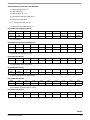
This is the pulse detection threshold value that can be set according to In Threshold Detection Mode the sensitivity is 16 counts/g.
The threshold is set in the LDTH $1A 8-bit Register.1.
$1B
PDTH
PDTH[7]
PDTH[6]
PDTH[5]
PDTH[4]
PDTH[3]
PDTH[2]
PDTH[1]
PDTH[0]
AN3468
Sensors
Freescale Semiconductor
22
This register defines the pulse width of the first pulse window. The pulse duration increments in ½ ms values, so every count is
½ ms. The total range is from 0-127.5ms.
$1C
PW
PD[7]
PD [6]
PD [5]
PD [4]
PD [3]
PD [2]
PD [1]
PD [0]
This register defines the latency time, which is the time in between pulses for double pulse, or the amount of time to trigger a
freefall condition. The scale increases from 0ms-255ms 0x00-0xFF. Every count is equal to 1ms.
$1D
LT
LT[7]
LT [6]
LT [5]
LT [4]
LT [3]
LT [2]
LT [1]
LT [0]
This is the timing window for the second pulse when setting up the double pulse condition. The scale is in ms increments from
0ms-255ms 0x00-0xFF.
$1E
TW
TW[7]
TW [6]
TW [5]
TW [4]
TW [3]
TW [2]
TW [1]
TW [0]
Optimal Settings for Single Pulse Detection
1. Positive OR logic: PDPL=0
2. X,Y,Z enabled
3. PDTH=0x40 (4g)
4. PD=0x10
1. Positive OR Logic PDPL=0
RegisterWrite(0x19,regs[0x19]&0xFD)
$19
CTL2
--
--
--
--
--
DRVO
PDPL
LDPL
$19
mask
1
1
1
1
1
1
0
1
$19
result
--
--
--
--
--
DRVO
0
LDPL
2. X,Y,Z enabled
RegisterWrite1(0x18,regs[0x18]&0x87)
$18
CTL1
DFBW
THOPT
ZDA
YDA
XDA
INTRG[1]
INTRG[0]
INTPIN
$18
mask
1
0
0
0
0
1
1
1
$18
result
DFBW
0
0
0
0
INTRG[1]
INTRG[0]
INTPIN
3. PDTH (Pulse Threshold) set to 4 g
RegisterWrite(0x1B,0x40)
$1B
PDTH
PDTH[7]
PDTH[6]
PDTH[5]
PDTH[4]
PDTH[3]
PDTH[2]
PDTH[1]
PDTH[0]
$1B
result
0
1
0
0
0
0
0
0
4. PD (Pulse Duration) set to 8 ms
RegisterWrite(0x1C,10)
$1C
PW
PD[7]
PD [6]
PD [5]
PD [4]
PD [3]
PD [2]
PD [1]
PD [0]
$1C
result
0
0
0
1
0
0
0
0
AN3468
Sensors
Freescale Semiconductor
23
Optimal Settings for Double Pulse Detection
1. Positive OR Logic PDPL = 0
2. Z axis enabled only
3. Pulse Threshold set to 4 g
4. Pulse Duration=$3C (60 counts) 30 ms
5. Latency Time=0x5A 90ms
6. 2nd Time Window 0x82 (130 ms)
1. Positive OR Logic Enabled PDPL = 0
RegisterWrite(0x19,regs[0x19]&0xFD)
$19
CTL2
--
--
--
--
--
DRVO
PDPL
LDPL
$19
mask
1
1
1
1
1
1
0
1
$19
result
--
--
--
--
--
DRVO
0
LDPL
2. Z only enabled
RegisterWrite(0x18,(regs[0x18]&0x98)|0x18)
$18
CTL1
DFBW
THOPT
ZDA
YDA
XDA
INTRG[1]
INTRG[0]
INTPIN
$18
mask
1
0
0
1
1
0
0
0
$18
result
DFBW
0
0
1
1
INTRG[1]
INTRG[0]
INTPIN
3. PDTH (Pulse Threshold) set to 4 g
RegisterWrite(0x1B,0x40)
$1B
PDTH
PDTH[7]
PDTH[6]
PDTH[5]
PDTH[4]
PDTH[3]
PDTH[2]
PDTH[1]
PDTH[0]
$1B
result
0
1
0
0
0
0
0
0
4. Pulse Duration for first pulse 30 ms
RegisterWrite(0x1C,0x3C)
$1C
PW
PD[7]
PD [6]
PD [5]
PD [4]
PD [3]
PD [2]
PD [1]
PD [0]
$1C
result
0
0
1
1
1
1
0
0
5. Latency time between the pulses 90 ms
RegisterWrite(0x1D,0x5A)
$1D
LT
LT[7]
LT [6]
LT [5]
LT [4]
LT [3]
LT [2]
LT [1]
LT [0]
$1D
result
0
1
0
1
1
0
1
0
6. Time Window for Second Pulse = 130 ms
ReigsterWrite(0x1E,0x82)
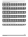
$1E
TW
TW[7]
TW [6]
TW [5]
TW [4]
TW [3]
TW [2]
TW [1]
TW [0]
$1E
result
1
0
0
0
0
0
1
0
AN3468
Sensors
Freescale Semiconductor
24
Table 2. User registers Summary
Address
Name
Bit 7
Bit 6
Bit 5
Bit 4
Bit 3
Bit 2
Bit 1
Bit 0
$00
XOUTL
XOUT[7]
XOUT[6]
XOUT[5]
XOUT[4]
XOUT[3]
XOUT[2]
XOUT[1]
XOUT[0]
$01
XOUTH
--
--
--
--
--
--
XOUT[9]
XOUT[8]
$02
YOUTL
YOUT[7]
YOUT[6]
YOUT[5]
YOUT[4]
YOUT[3]
YOUT[2]
YOUT[1]
YOUT[0]
$03
YOUTH
--
--
--
--
--
--
YOUT[9]
YOUT[8]
$04
ZOUTL
ZOUT[7]
ZOUT[6]
ZOUT[5]
ZOUT[4]
ZOUT[3]
ZOUT[2]
ZOUT[1]
ZOUT[0]
$05
ZOUTH
--
--
--
--
--
--
ZOUT[9]
ZOUT[8]
$06
XOUT8
XOUT[7]
XOUT[6]
XOUT[5]
XOUT[4]
XOUT[3]
XOUT[2]
XOUT[1]
XOUT[0]
$07
YOUT8
YOUT[7]
YOUT[6]
YOUT[5]
YOUT[4]
YOUT[3]
YOUT[2]
YOUT[1]
YOUT[0]
$08
ZOUT8
ZOUT[7]
ZOUT[6]
ZOUT[5]
ZOUT[4]
ZOUT[3]
ZOUT[2]
ZOUT[1]
ZOUT[0]
$09
STATUS
--
--
--
--
--
PERR
DOVR
DRDY
$0A
DETSRC
LDX
LDY
LDZ
PDX
PDY
PDZ
INT2
INT1
$0B
TOUT
TMP[7]
TMP[6]
TMP[5]
TMP[4]
TMP[3]
TMP[2]
TMP[1]
TMP[0]
$0C
--
--
--
--
--
--
--
--
--
$0D
I2CAD
I2CDIS
DAD[6]
DAD[5]
DAD[4]
DAD[3]
DAD[2]
DAD[1]
DAD[0]
$0E
USRINF
UI[7]
UI[6]
UI[5]
UI[4]
UI[3]
UI[2]
UI[1]
UI[0]
$0F
WHOAM
ID[7]
ID[6]
ID[5]
ID[4]
ID[3]
ID[2]
ID[1]
ID[0]
$10
XOFFL
XOFF[7]
XOFF[6]
XOFF[5]
XOFF[4]
XOFF[3]
XOFF[2]
XOFF[1]
XOFF[0]
$11
XOFFH
--
--
--
--
--
XOFF[10]
XOFF[9]
XOFF[8]
$12
YOFFL
YOFF[7]
YOFF[6]
YOFF[5]
YOFF[4]
YOFF[3]
YOFF[2]
YOFF[1]
YOFF[0]
$13
YOFFH
--
--
--
--
--
YOFF[10]
YOFF[9]
YOFF[8]
$14
ZOFFL
ZOFF[7]
ZOFF[6]
ZOFF[5]
ZOFF[4]
ZOFF[3]
ZOFF[2]
ZOFF[1]
ZOFF[0]
$15
ZOFFH
--
--
--
--
--
ZOFF[10]
ZOFF[9]
ZOFF[8]
$16
MCTL
LPEN
DRPD
SPI3W
STON
GLVL[1]
GLVL[0]
MOD[[1]]
MOD[0]
$17
INTRST
--
--
--
--
--
--
CLRINT2
CLRINT1
$18
CTL1
DFBW
THOPT
ZDA
YDA
XDA
INTRG[1]
INTRG[0]
INTPIN
$19
CTL2
--
--
--
--
--
DRVO
PDPL
LDPL
$1A
LDTH
LDTH[7]
LDTH[6]
LDTH[5]
LDTH[4]
LDTH[3]
LDTH[2]
LDTH[1]
LDTH[0]
$1B
PDTH
PDTH[7]
PDTH[6]
PDTH[5]
PDTH[4]
PDTH[3]
PDTH[2]
PDTH[1]
PDTH[0]
$1C
PW
PD[7]
PD [6]
PD [5]
PD [4]
PD [3]
PD [2]
PD [1]
PD [0]
$1D
LT
LT[7]
LT [6]
LT [5]
LT [4]
LT [3]
LT [2]
LT [1]
LT [0]
$1E
TW
TW[7]
TW [6]
TW [5]
TW [4]
TW [3]
TW [2]
TW [1]
TW [0]
$1F
--
--
--
--
--
--
--
--
--
NOTES:
1. http://www.esacademy.com/faq/i2c/general/i2cpseud.htm
AN3468
Sensors
Freescale Semiconductor
25
How to Reach Us:
Home Page:
www.freescale.com
Web Support:
http://www.freescale.com/support
USA/Europe or Locations Not Listed:
Freescale Semiconductor, Inc.
Technical Information Center, EL516
2100 East Elliot Road
Tempe, Arizona 85284
1-800-521-6274 or +1-480-768-2130
www.freescale.com/support
Europe, Middle East, and Africa:
Freescale Halbleiter Deutschland GmbH
Technical Information Center
Schatzbogen 7
81829 Muenchen, Germany
+44 1296 380 456 (English)
+46 8 52200080 (English)
+49 89 92103 559 (German)
+33 1 69 35 48 48 (French)
www.freescale.com/support
Japan:
Freescale Semiconductor Japan Ltd.
Headquarters
ARCO Tower 15F
1-8-1, Shimo-Meguro, Meguro-ku,
Tokyo 153-0064
Japan
0120 191014 or +81 3 5437 9125
[email protected]
Asia/Pacific:
Freescale Semiconductor China Ltd.
Exchange Building 23F
No. 118 Jianguo Road
Chaoyang District
Beijing 100022
China
+86 010 5879 8000
[email protected]
For Literature Requests Only:
Freescale Semiconductor Literature Distribution Center
P.O. Box 5405
Denver, Colorado 80217
1-800-441-2447 or +1-303-675-2140
Fax: +1-303-675-2150
[email protected]
AN3468
Rev. 0
08/2008
Information in this document is provided solely to enable system and software
implementers to use Freescale Semiconductor products. There are no express or
implied copyright licenses granted hereunder to design or fabricate any integrated
circuits or integrated circuits based on the information in this document.
Freescale Semiconductor reserves the right to make changes without further notice to
any products herein. Freescale Semiconductor makes no warranty, representation or
guarantee regarding the suitability of its products for any particular purpose, nor does
Freescale Semiconductor assume any liability arising out of the application or use of any
product or circuit, and specifically disclaims any and all liability, including without
limitation consequential or incidental damages. “Typical” parameters that may be
provided in Freescale Semiconductor data sheets and/or specifications can and do vary
in different applications and actual performance may vary over time. All operating
parameters, including “Typicals”, must be validated for each customer application by
customer’s technical experts. Freescale Semiconductor does not convey any license
under its patent rights nor the rights of others. Freescale Semiconductor products are
not designed, intended, or authorized for use as components in systems intended for
surgical implant into the body, or other applications intended to support or sustain life,
or for any other application in which the failure of the Freescale Semiconductor product
could create a situation where personal injury or death may occur. Should Buyer
purchase or use Freescale Semiconductor products for any such unintended or
unauthorized application, Buyer shall indemnify and hold Freescale Semiconductor and
its officers, employees, subsidiaries, affiliates, and distributors harmless against all
claims, costs, damages, and expenses, and reasonable attorney fees arising out of,
directly or indirectly, any claim of personal injury or death associated with such
unintended or unauthorized use, even if such claim alleges that Freescale
Semiconductor was negligent regarding the design or manufacture of the part.
Freescale™ and the Freescale logo are trademarks of Freescale Semiconductor, Inc.
All other product or service names are the property of their respective owners.
© Freescale Semiconductor, Inc. 2008. All rights reserved.