1
UM1057
User manual
STM3220G-EVAL evaluation board
Introduction
The STM3220G-EVAL evaluation board is a complete demonstration and development
platform for the STM32F2 series and includes an embedded STM32F207IGH6 highperformance ARM®Cortex™-M3 32-bit microcontroller .
The full range of hardware features on the board is provided to help you evaluate all
peripherals (USB OTG HS, USB OTG FS, ethernet, motor control, CAN, MicroSD Card™,
smartcard, USART, Audio DAC, RS-232, IrDA, SRAM, MEMS, EEPROM… etc.) and
develop your own applications. Extension headers make it possible to easily connect a
daughter board or wrapping board for your specific application.
The in-circuit ST-LINK tool can be easily used for JTAG and SWD interface debugging and
programming.
Figure 1.
January 2012
STM3220G-EVAL evaluation board
Doc ID 018499 Rev 5
1/66
www.st.com
Contents
UM1057
Contents
1
2
3
Overview . . . . . . . . . . . . . . . . . . . . . . . . . . . . . . . . . . . . . . . . . . . . . . . . . . 4
1.1
Features . . . . . . . . . . . . . . . . . . . . . . . . . . . . . . . . . . . . . . . . . . . . . . . . . . . 4
1.2
Demonstration software . . . . . . . . . . . . . . . . . . . . . . . . . . . . . . . . . . . . . . . 4
1.3
Order code . . . . . . . . . . . . . . . . . . . . . . . . . . . . . . . . . . . . . . . . . . . . . . . . . 4
1.4
Delivery recommendations . . . . . . . . . . . . . . . . . . . . . . . . . . . . . . . . . . . . . 5
Hardware layout and configuration . . . . . . . . . . . . . . . . . . . . . . . . . . . . . 6
2.1
Power supply . . . . . . . . . . . . . . . . . . . . . . . . . . . . . . . . . . . . . . . . . . . . . . . 9
2.2
Boot option . . . . . . . . . . . . . . . . . . . . . . . . . . . . . . . . . . . . . . . . . . . . . . . . 10
2.3
Clock source . . . . . . . . . . . . . . . . . . . . . . . . . . . . . . . . . . . . . . . . . . . . . . . 11
2.4
Reset source . . . . . . . . . . . . . . . . . . . . . . . . . . . . . . . . . . . . . . . . . . . . . . 11
2.5
Audio . . . . . . . . . . . . . . . . . . . . . . . . . . . . . . . . . . . . . . . . . . . . . . . . . . . . 11
2.6
EEPROM . . . . . . . . . . . . . . . . . . . . . . . . . . . . . . . . . . . . . . . . . . . . . . . . . 12
2.7
CAN . . . . . . . . . . . . . . . . . . . . . . . . . . . . . . . . . . . . . . . . . . . . . . . . . . . . . 12
2.8
RS-232 and IrDA . . . . . . . . . . . . . . . . . . . . . . . . . . . . . . . . . . . . . . . . . . . 13
2.9
Motor control . . . . . . . . . . . . . . . . . . . . . . . . . . . . . . . . . . . . . . . . . . . . . . 14
2.10
Smartcard . . . . . . . . . . . . . . . . . . . . . . . . . . . . . . . . . . . . . . . . . . . . . . . . . 15
2.11
MicroSD Card . . . . . . . . . . . . . . . . . . . . . . . . . . . . . . . . . . . . . . . . . . . . . . 15
2.12
MEMS . . . . . . . . . . . . . . . . . . . . . . . . . . . . . . . . . . . . . . . . . . . . . . . . . . . . 16
2.13
Potentiometer . . . . . . . . . . . . . . . . . . . . . . . . . . . . . . . . . . . . . . . . . . . . . . 16
2.14
ADC . . . . . . . . . . . . . . . . . . . . . . . . . . . . . . . . . . . . . . . . . . . . . . . . . . . . . 16
2.15
USB OTG FS . . . . . . . . . . . . . . . . . . . . . . . . . . . . . . . . . . . . . . . . . . . . . . 16
2.16
Ethernet . . . . . . . . . . . . . . . . . . . . . . . . . . . . . . . . . . . . . . . . . . . . . . . . . . 17
2.17
USB OTG HS . . . . . . . . . . . . . . . . . . . . . . . . . . . . . . . . . . . . . . . . . . . . . . 18
2.18
Camera module . . . . . . . . . . . . . . . . . . . . . . . . . . . . . . . . . . . . . . . . . . . . 18
2.19
SRAM . . . . . . . . . . . . . . . . . . . . . . . . . . . . . . . . . . . . . . . . . . . . . . . . . . . . 19
2.20
Development and debug support . . . . . . . . . . . . . . . . . . . . . . . . . . . . . . . 20
2.21
Display and input devices . . . . . . . . . . . . . . . . . . . . . . . . . . . . . . . . . . . . . 21
Connectors . . . . . . . . . . . . . . . . . . . . . . . . . . . . . . . . . . . . . . . . . . . . . . . 22
3.1
2/66
Daughter board extension connectors CN1, 2, 3 and 4 . . . . . . . . . . . . . . 22
Doc ID 018499 Rev 5
UM1057
Contents
3.2
Motor control connector CN5 . . . . . . . . . . . . . . . . . . . . . . . . . . . . . . . . . . 29
3.3
MicroSD connector CN6 . . . . . . . . . . . . . . . . . . . . . . . . . . . . . . . . . . . . . . 30
3.4
Ethernet RJ45 connector CN7 . . . . . . . . . . . . . . . . . . . . . . . . . . . . . . . . . 30
3.5
USB OTG FS Micro-AB connector CN8 . . . . . . . . . . . . . . . . . . . . . . . . . . 31
3.6
USB OTG HS Micro-AB connector CN9 . . . . . . . . . . . . . . . . . . . . . . . . . 31
3.7
CAN D-type 9-pin male connectors CN10 (CAN1 or CAN2) . . . . . . . . . . 32
3.8
Audio connector CN11 . . . . . . . . . . . . . . . . . . . . . . . . . . . . . . . . . . . . . . . 32
3.9
Trace debugging connector CN13 . . . . . . . . . . . . . . . . . . . . . . . . . . . . . . 32
3.10
JTAG debugging connector CN14 . . . . . . . . . . . . . . . . . . . . . . . . . . . . . . 33
3.11
Camera module connector CN15 . . . . . . . . . . . . . . . . . . . . . . . . . . . . . . . 34
3.12
RS-232 connector CN16 . . . . . . . . . . . . . . . . . . . . . . . . . . . . . . . . . . . . . 35
3.13
Power connector CN18 . . . . . . . . . . . . . . . . . . . . . . . . . . . . . . . . . . . . . . 35
3.14
TFT LCD connector CN19 . . . . . . . . . . . . . . . . . . . . . . . . . . . . . . . . . . . . 35
3.15
Smartcard connector CN20 . . . . . . . . . . . . . . . . . . . . . . . . . . . . . . . . . . . 36
3.16
ST-LINK/V2 connector CN21 . . . . . . . . . . . . . . . . . . . . . . . . . . . . . . . . . . 36
3.17
Camera extension connector CN23 . . . . . . . . . . . . . . . . . . . . . . . . . . . . . 36
3.18
STM3220G-EVAL pinout . . . . . . . . . . . . . . . . . . . . . . . . . . . . . . . . . . . . . 37
4
Schematics . . . . . . . . . . . . . . . . . . . . . . . . . . . . . . . . . . . . . . . . . . . . . . . 43
5
Revision history . . . . . . . . . . . . . . . . . . . . . . . . . . . . . . . . . . . . . . . . . . . 65
Doc ID 018499 Rev 5
3/66
Overview
UM1057
1
Overview
1.1
Features
1.2
■
STM32F207IGH6 microcontroller
■
16 Mbit SRAM
■
1 Gbyte or more MicroSD Card
■
Boot from user Flash, system memory or SRAM
■
Both ISO/IEC 14443 type A and B smartcard support
■
I2C compatible serial interface 8 Kbytes EEPROM, MEMS and I/O expander
■
IEEE 802.3-2002 compliant ethernet connector
■
Two CAN 2.0 A/B channels on the same DB connector
■
RS-232 communication
■
IrDA transceiver
■
USB OTG (HS and FS) with Micro-AB connector
■
Inductor motor control connector
■
I2S Audio DAC, stereo audio jack for headset
■
3.2" 240x320 TFT color LCD with touchscreen
■
4 color LEDs
■
Camera module and extension connector for ST camera plug-in
■
Joystick with 4-direction control and selector
■
Reset, wakeup, tamper and user button
■
RTC with backup battery
■
Extension connector for daughterboard or wrapping board
■
JTAG, SW and trace debug support
■
Embedded ST-LINK/V2
■
Five 5V power supply options: Power jack, USB FS connector, USB HS connector,
ST-LINK/V2 or daughterboard
■
MCU consumption measurement circuit
Demonstration software
Demonstration software is preloaded in the board's Flash memory for easy demonstration of
the device peripherals in standalone mode. For more information and to download the latest
version, please refer to STM3220G-EVAL demonstration software available on web:
www.st.com/mcu
1.3
Order code
To order the STM32F207IGH6 MCU evaluation board, use the order code STM3220GEVAL.
4/66
Doc ID 018499 Rev 5
UM1057
1.4
Overview
Delivery recommendations
Several verifications are needed before using the board for the first time to make sure that
nothing has been damaged during shipment and no components are unplugged and lost.
When the board is extracted from its plastic bag, please check that no component remains
in the bag. Main components to verify are:
1.
The 25 MHz crytals (X1 and X4) may have been removed by a shock.
2.
The camera connected on socket CN15 located on the right side of the board under the
JTAG connector may be unplugged. If this is the case, please refer to the note in
Section 2.18: Camera module to make sure to replug it in the correct position.
3.
The MicroSD Card may have been ejected from its connector CN6 (top left corner of
the board).
The plastic protection on the camera should be removed carefully as the connection is very
fragile.
Doc ID 018499 Rev 5
5/66
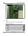
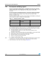
Hardware layout and configuration
2
UM1057
Hardware layout and configuration
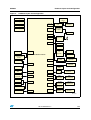
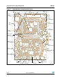
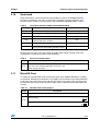
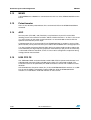
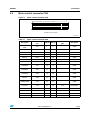
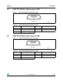
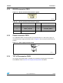
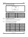
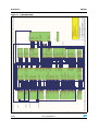
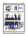
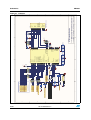
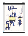
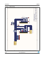
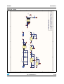
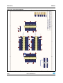
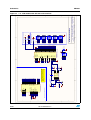
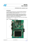
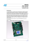
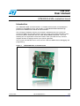
The STM3220G-EVAL evaluation board is designed around the STM32F207IGH6 in the
UFBGA176 package. Figure 2 illustrates the connection between STM32F207IGH6 and
peripherals (camera module, LCD, SRAM, EEPROM, MEMS, USART, IrDA, USB OTG HS,
USB OTG FS, Ethernet, Audio, CAN bus, Smart card, MicroSD Card and motor control) and
Figure 3 helps you locate these features on the actual evaluation board.
6/66
Doc ID 018499 Rev 5
UM1057
Hardware layout and configuration
Figure 2.
Hardware layout and configuration
9UHJXODWRU
86%SRZHU
VZLWFK
9UHJXODWRU
27*+6
9UHJXODWRU
$'&
9UHJXODWRU
86%+6
3+<
86%0LFUR$%
FRQQHFWRU
0LFURSKRQH
$PSOLILHU
$XGLR-DFN
'$&
,6
,&
$XGLR'$&
0(06
((3520
/('V.H\
,2
H[SDQGHU
*3,2
670),*+
([WHQVLRQ
FRQQHFWRUIRU
*3,2V
7RXFKVFUHHQ
'&0,
65$0
)60&
-R\VWLFN
&DPHUD
PRGXOH
&DPHUDH[WHQVLRQ
FRQQHFWRU
86%0LFUR$%
FRQQHFWRU
27*)6
86%SRZHU
VZLWFK
7)7/&'
0LFUR6'
FDUG
6',2
0&FRQWURO
FRQQHFWRU
0&
0,,50,,
&$1
&$1
3+<
,QWHJUDWHG5-
FRQQHFWRU
&$1
WUDQVFHLYHU
&$1
'%FRQQHFWRU
56
WUDQVFHLYHU
56
'%FRQQHFWRU
-7$*
'HEXJ
7UDFH
86$57
67/,1.9
3RWHQWLRPHWHU
$'&
86$57
,U'$
WUDQVFHLYHU
6PDUWFDUG
LQWHUIDFH
6PDUWFDUG
FRQQHFWRU
069
Doc ID 018499 Rev 5
7/66
Hardware layout and configuration
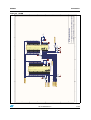
Figure 3.
UM1057
STM3220G-EVAL evaluation board layout
%!&
3
!
"
#$%
#$&
'(!)*
3
'
7-.
CONNECTOR $4"
(
,60
++,
"
1560
+-.
3
4+
#
3.
8/66
#
20,1
+
#
+1
Doc ID 018499 Rev 5
#
.0/
/.0
UM1057
2.1
Hardware layout and configuration
Power supply
The STM3220G-EVAL evaluation board is designed to be powered by a 5 V DC power
supply and to be protected by PolyZen from a wrong power plug-in event. It is possible to
configure the evaluation board to use any of following five sources for the power supply:
●
5 V DC power adapter connected to JP18, the power jack on the board
●
5 V DC power with 500 mA limitation from CN8, the USB OTG FS Micro-AB connector
●
5 V DC power with 500 mA limitation from CN9, the USB OTG HS Micro-AB connector
●
5 V DC power with 500 mA limitation from CN21, the ST-LINK/V2 USB connector
●
5 V DC power from both CN1 and CN3, the extension connector for daughterboard
(DTB for daughterboard on silkscreen)
The power supply is configured by setting the related jumpers JP4, JP32, JP18 and JP19 as
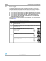
described in Table 1.
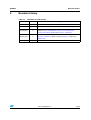
Table 1.
Jumper
Power related jumpers and solder bridges
Description
JP4
Jumper reserved for future use (RFU).
Default setting: Fitted
JP32
MCU_VDD is connected to 3.3 V power when JP32 is closed and MCU current
consumption measurement can be done manually by a multimeter when JP32 is open.
Default setting: Fitted
JP18 selects one of the five possible power supply sources. To
select the ST-LINK/V2 USB connector (CN21) power supply,
set JP18 as shown:
(Default setting)
HS
FS
DTB
PSU
STlk
To select power supply jack (CN18) power supply, set JP18
as shown:
HS
FS
DTB
PSU
STlk
JP18
To select daughterboard connector (CN1 and CN3) power
supply, set JP18 as shown:
Doc ID 018499 Rev 5
HS
FS
DTB
PSU
STlk
9/66
Hardware layout and configuration
Table 1.
UM1057
Power related jumpers and solder bridges (continued)
Jumper
Description
To select USB OTG FS (CN8) power supply, set JP18 as
shown:
To select USB OTG HS (CN9) power supply, set JP18 as
shown:
JP18
(cont.)
To select power supply jack (CN18) power supply to both
STM3220G-EVAL and daughterboard connected on CN1 and
CN3, set JP18 as shown (daughterboard must not have its
own power supply connected)
HS
FS
DTB
PSU
STlk
HS
FS
DTB
PSU
STlk
HS
FS
DTB
PSU
STlk
To connect Vbat to the battery, set JP19 as shown:
JP19
1 2 3
To connect Vbat to 3.3 V power, set JP19 as shown:
(Default setting)
1 2 3
Note:
LED LD9 is lit when the STM3220G-EVAL evaluation board is powered by the 5 V correctly.
2.2
Boot option
The STM3220G-EVAL evaluation board is able to boot from:
●
Embedded user Flash
●
System memory with boot loader for ISP
●
Embedded SRAM for debugging
The boot option is configured by setting switch SW1 (BOOT1) and SW2 (BOOT0). The
BOOT0 can be configured also via the RS-232 connector CN16.
Table 2.
10/66
Boot related jumpers
BOOT 0
BOOT 1
Boot source
0
0 or 1
1
1
STM3220G-EVAL boots from Embedded SRAM
1
0
STM3220G-EVAL boots from System Memory
STM3220G-EVAL boots from User Flash (Default setting)
Doc ID 018499 Rev 5
UM1057
2.3
Hardware layout and configuration
Clock source
Four clock sources are available on the STM3220G-EVAL evaluation board for the
STM32F207IGH6 and embedded RTC:
2.4
●
X1, 25 MHz crystal for ethernet PHY with socket. It can be removed when clock is
provided by MCO pin of the MCU
●
X2, 26 MHz crystal for USB OTG HS PHY
●
X3, 32 kHz crystal for embedded RTC
●
X4, 25 MHz crystal with socket for the STM32F207IGH6 microcontroller. (It can be
removed from socket when internal RC clock is used.)
Reset source
The reset signal of the STM3220G-EVAL evaluation board is low active and the reset
sources include:
2.5
●
Reset button B1
●
Debugging tools from JTAG connector CN14 and trace connector CN13
●
Daughterboard from CN3
●
RS-232 connector CN16 for ISP
●
ST-LINK/V2
Audio
The STM3220G-EVAL evaluation board enables stereo audio play and microphone
recording by an external headset connected on audio jack CN11. An audio DAC CS43L22 is
connected to both an I2S2 port and a DAC channel while a microphone amplifier is
connected to the ADC of the STM32F207IGH6. The CS43L22 can be configured via I2C1
and external PLL (U36) can provide an external clock which is connected to I2S_CKIN pin
(PC9).
Note:
To avoid speaker damage it is mandatory to connect the headphone to the board on CN11
during audio code debug. When the program is stopped on a breakpoint, a DC voltage may
be applied to the speaker which induces power consumption incompatible with the speaker.
Warning:
Table 3.
Jumper
Signal I2S_SD (PI3) is close to signal TCK/SWCLK of the
JTAG/SWD interface, so to avoid possible communication
issues on JTAG/SWD when the I2S interface is used the
recommendations are to:
1) Prefer usage of embedded ST-LINK/V2 to external tool
connected on CN14.
2) Configure PI3 GPIO in low speed (2 MHz or 10 MHz).
Audio related jumpers
Description
JP16
Description of JP16 is in Table 10 on page 15.
JP33
The microphone amplifier can be disabled when JP33 is fitted. Default setting: Not fitted.
Doc ID 018499 Rev 5
11/66
Hardware layout and configuration
2.6
UM1057
EEPROM
A 64 KBit EEPROM is connected to the I2C1 bus of the STM32F207IGH6.
Table 4.
EEPROM related jumper and solder bridge
Jumper
JP24
2.7
Description
The EEPROM is in Write Protection mode when JP24 is not fitted.
Default setting: Not fitted.
CAN
The STM3220G-EVAL evaluation board enables two channels of CAN2.0A/B compliant
CAN bus communication based on a 3.3 V CAN transceiver on one DB9 connector (CN10).
The two CAN buses can be disconnected by jumpers from relevant STM32F207IGH6 I/Os
which are shared with FSMC and USB OTG HS. Jumpers JP3 and JP10 must be refitted to
enable CAN1 or CAN2 as listed in Table 5.
High-speed, Standby and Slope Control modes are selected by setting JP7.
Table 5.
Jumper
CAN-related jumpers
Description
To connect CAN1_TX to CAN transceiver, set JP3 as shown:
JP3
To connect CAN2_TX to CAN transceiver, set JP3 as shown:
To connect CAN1_RX to CAN transceiver, set JP10 as shown:
JP10
To connect CAN2_RX to CAN transceiver, set JP10 as shown:
1 2 3
1 2 3
1 2 3
1 2 3
PD0 and PB5 are disconnected from the CAN transceiver and used for FSMC and
USB_OTG_HS when jumper JP10 is not fitted (Default setting).
To enable the selected CAN transceiver to work in Standby mode, set JP7 as
shown:
JP7
To enable the selected CAN transceiver to work in High-speed mode, set JP7 as
shown (Default setting):
1 2 3
1 2 3
To enable the selected CAN transceiver to work in Slope Control mode, do not fit a jumper
on JP7.
JP9
12/66
To enable the terminal resistor for the selected CAN, fit a jumper on JP9.
(Default setting: Not fitted).
Doc ID 018499 Rev 5
UM1057
2.8
Hardware layout and configuration
RS-232 and IrDA
Both RS-232 and IrDA communication is enabled by a D-type 9-pin RS-232 connector
(CN16) and IrDA transceiver U11 which are connected to USART3 of the STM32F207IGH6
on the STM3220G-EVAL evaluation board.
For ISP support, two signals are added on the RS-232 connector CN16:
●
Bootloader_RESET (shared with CTS signal)
●
Bootloader_BOOT0 (shared with DSR signal)
RS-232 or IrDA can be selected by setting JP22 and ISP can be enabled by setting JP29
and JP34.
Table 6.
Jumper
RS-232 and IrDA related jumper
Description
To connect USART3_RX to IrDA transceiver and enable IrDA communication,
set JP22 as shown:
JP22
To connect USART3_RX to RS-232 transceiver and enable RS-232
communication, set JP22 as shown (Default setting):
1 2 3
1 2 3
To enable MicroSD Card, which shares same I/Os with RS-232, JP22 is not fitted.
JP29
Bootloader_BOOT0 is managed by pin 6 of CN16 (RS-232 DSR signal) when JP29 is
closed. This configuration is used for boot loader application only.
Default setting: Not fitted.
JP34
Bootloader_RESET is managed by pin 8 of CN16 (RS-232 CTS signal) when JP34 is
fitted. This configuration is used for boot loader application only.
Default setting: Not fitted.
Doc ID 018499 Rev 5
13/66
Hardware layout and configuration
2.9
UM1057
Motor control
The STM3220G-EVAL evaluation board enables a three-phase brushless motor control via
a 34-pin connector (CN5), which provides all required control and feedback signals to and
from the motor power-driving board. Available signals on this connector include emergency
stop, motor speed, 3-phase motor current, bus voltage, heatsink temperature coming from
the motor driving board and 6 channels of PWM control signal going to the motor driving
circuit.
The solder bridge (SB18) allows to choose two kinds of synchronization methods for PFCs
(Power Factor Correction) while SB17 can be set for different signals on pin 31 of CN5.
The I/O pins used on motor control connector CN5 are multiplexed with some peripherals on
the board; either motor control connector or multiplexed peripherals can be enabled by the
setting of solder bridges SB10, SB11, SB12, SB14, SB15 and SB16.
Table 7.
Motor control solder bridges
Solder
bridge
Description
SB18
When closed, SB18 redirects the PFC synchronized signal to the timer 3
input capture pin 2 in addition to the timer 3 external trigger input.
Default setting: Open
SB17
For CN5 encoder signal input (pin 31), SB17 must be open.
For CN5 special motor analog signal input (pin 31), SB17 must be closed.
Default setting: Open
SB16
To connect MC_EmergencySTOP to PI4, close SB16.
Default setting: Open
SB10
To connect MC_EnIndex to PB8, close SB10.
Default setting: Open
SB11
To connect MC_CurrentA to PC1, close SB11.
Default setting: Open
SB12
To connect MC_CurrentB to PC2, close SB12.
Default setting: Open
SB14
To connect MC_EnB to PD13, close SB14.
Default setting: Open
SB15
To connect MC_EnA to PD12 close SB15.
Default setting: Open
Multiplexed
peripherals
Camera module
connected to
CN15
Ethernet
FSMC
Note:
1
Some 0 ohm resistors have to be removed or soldered to enable motor control application
except the solder bridges configurations mentioned above:
– R34, R58 & R51 to be removed
– R66, R204 & R205 to be soldered
2
14/66
The MicroSD Card must be removed from CN6 for motor control application.
Doc ID 018499 Rev 5
UM1057
2.10
Hardware layout and configuration
Smartcard
STMicroelectronics smartcard interface chip ST8024 is used on the STM3220G-EVAL
board for asynchronous 3 V and 5 V smartcards. It performs all supply protection and
control functions based on the connections with the STM32F207IGH6 listed in Table 8:
Table 8.
Connection between ST8024 and STM32F207IGH6
ST8024 signals
Description
Connect to STM32F207IGH6
5V/3V
Smartcard power supply selection pin
PH15
I/OUC
MCU data I/O line
PC6
XTAL1
Crystal or external clock input
PG7
Detect presence of a card, MCU interrupt, share
same pin with motor controller
PF6
Card reset input from MCU
PF7
OFF
RSTIN
CMDVCC
Start activation sequence input (Active Low),
share same pin with I2S DAC and Motor control
PG12
Smartcard shares some I/Os with I2S bus for Audio. Some jumper settings need to be
reconfigured to enable smartcard as indicated below:
Table 9.
Smartcard related jumper
Jumper
JP21
2.11
Description
To connect Smartcard_IO to PC6, JP21must be fitted.
JP21 must not be fitted for Audio DAC connection to I2S.
Default setting: Not Fitted
MicroSD Card
A 1 GByte or more MicroSD Card connected to SDIO of the STM32F207IGH6 is available
on the board. MicroSD Card detection is managed by the standard I/O port PH13. MicroSD
Card shares I/Os with motor control, RS-232 and audio. The jumpers JP22 and JP16 must
be refitted and the motor control connector (CN5) must be disconnected for MicroSD Card
function.
Table 10.
Jumper
JP22
MicroSD Card related jumpers
Description
Description of JP22 is in Section 2.8: RS-232 and IrDA
PC9 is connected to MicroSDCard_D1 when JP16 is set as shown to the right:
(Default setting):
1 2 3
JP16
PC9 is connected to I2S_CKIN when JP16 is set as show to the right:
Doc ID 018499 Rev 5
1 2 3
15/66
Hardware layout and configuration
2.12
UM1057
MEMS
A ST MEMS device LIS302DL is connected to the I2C1 bus of the STM32F207IGH6 on the
board.
2.13
Potentiometer
There is one 10 Kohm potentiometer, RV1, connected to PF9 of the STM32F207IGH6 on
the board.
2.14
ADC
Two test points (TP3 AIN-) and (TP4 AIN+) are placed close to port PC1 of the MCU
allowing precise measurements on ADC1, ADC2 or ADC3 channel 11. As PC1 is also used
as current A input on the motor control connector it is recommended to remove R219 to
optimize noise immunity on this input.
A potentiometer RV1 is connected to PF9 of STM32F207IGH6. If needed, a low pass filter
(R74 and C59) can be placed on this input to reduce the bandwidth of the analog input PF9.
It is also possible to place the Ethernet PHY (U5) in low power mode in order to reduce the
noise induced by this high frequency peripheral. Power down pin (MII_INT in the schematic)
is connected to PB14 of the MCU, so this I/O can be to be configured as output low during
analog precision measurement.
2.15
USB OTG FS
The STM3220G-EVAL evaluation board enables USB OTG full speed communication via a
USB Micro-AB connector (CN8) and USB power switch (U1) connected to VBUS. The
evaluation board can be powered by this USB connection at 5V DC with a 500 mA current
limitation.
LED LD6 indicates that power switch (U1) is ON and STM3220G-EVAL functions as a USB
host or that the VBUS is powered by another USB host while the STM3220G-EVAL
functions as a USB device. LED LD5 indicates an over-current.
16/66
Doc ID 018499 Rev 5
UM1057
2.16
Hardware layout and configuration
Ethernet
The STM3220G-EVAL evaluation board enables 10/100M ethernet communication by a
PHY DP83848CVV (U5) and integrated RJ45 connector (CN7). Both MII and RMII interface
modes can be selected by setting jumpers JP5, JP6 and JP8 as listed below:
Table 11.
Jumper
JP8
Ethernet related jumpers and solder bridges
Description
JP8 selects MII or RMII interface mode.
To enable MII, JP8 is not fitted. To enable RMII interface mode, JP8 is fitted.
Default setting: Not fitted
To enable MII interface mode, set JP6 as shown (Default setting):
JP6
To enable RMII interface mode, set JP6 as shown:
To provide 25 MHz clock for MII or 50 MHz clock for RMII by MCO at PA8, set
JP5 as shown (Default setting):
JP5
To provide 25 MHz clock by external crystal X1 (for MII interface mode only) set
JP5 as shown:
1 2 3
1 2 3
1 2 3
1 2 3
When clock is provided by external oscillator U3, JP5 must not be fitted (Default setting).
SB1
Note:
SB1 is used to select clock source only for RMII mode.
To connect the clock from MCO to RMII_REF_CLK, close SB1. The resistor R212 has to
be removed in this case.
Default setting: Open
1
A test point (TP2) is available on the board for the PTP_PPS feature test.
2
The Ethernet PHY U5 can be powered down by regulating PB14.
3
In RMII mode it is not possible to use MCO to output the 50 MHz clock to PHY due to the
PLL limitation explained in chapter 2.6.5 of STM32F20x & STM32F21x Errata sheet
(ES0005). In such a case it is possible to provide the 50 MHz clock by soldering a 50 MHz
oscillator (ref SM7745HEV-50.0M or equivalent) on the U3 footprint located under CN3 and
also removing jumper on JP5. This oscillator is not provided with the board.
Doc ID 018499 Rev 5
17/66
Hardware layout and configuration
2.17
UM1057
USB OTG HS
The STM3220G-EVAL evaluation board enables USB OTG high speed communication via a
USB Micro-AB connector (CN9), USB high speed PHY (U8) and USB power switch (U4)
connected to VBUS. The evaluation board can be powered by this USB connector (CN9) at
5 V DC with a 500 mA current limitation.
The LED LD7 indicates that power switch (U4) is On and that the STM3220G-EVAL is
working as a USB host or that VBUS is powered by another USB host when STM3220GEVAL is working as a USB device. The LD8 indicates an over-current.
The USB ULPI bus is shared with CAN2 bus, JP10 and JP3 must be open for USB OTG HS.
Table 12.
MicroSD Card related jumper
Jumper
JP31
Description
To disable USB OTG PHY U8, remove JP31. Default setting: Fitted
Note:
On boards MB786 prior to version B03 it is possible that after a board RESET the MCU is no
longer able to control communication with the OTG PHY (U8). When this issue occurs the
only way to recover OTG PHY control is to power the board OFF and ON. This issue is fixed
on MB786 version B03 or newer.
2.18
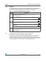
Camera module
A camera module is connected to the DCMI bus of the STM32F207IGH6 and shares the
same I/Os with the motor control connector. SB16 must be kept open for camera module
application.
There are two possible modules and omnivision cameras populated on the CN15 connector
of the board:
●
1.3 Megapixel: Module CN01302H1045-C: Camera OV9655
●
2 Megapixel: Module CN020VAH2554-C: Camera OV2640
Table 13.
Jumper
Note:
Camera module related jumpers
Description
JP26
To set power down mode for the camera module, JP26 is fitted.
Default setting: Not fitted
SB16
Description of SB16 is in Section 2.9: Motor control.
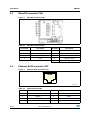
1
When the camera demo loaded in Flash is executed, some green pixels may appear in high
contrast zones, depending on the image captured.
2
The camera is not firmly restricted on its connector (CN15). It is possible that during
shipment the camera could be unplugged. In such case you need to plug it into the right
position as shown on the picture below (pin 1 dot on top left corner of the socket).
It is not recommended to remove it in order to avoid false contact later.
18/66
Doc ID 018499 Rev 5
UM1057
Hardware layout and configuration
Figure 4.
Pin 1 camera plug
The camera extension connector CN23 is available on the boards to connect the ST camera
plug-in board.
2.19
SRAM
The 16 Mbit SRAM is connected to the FSMC bus of the STM32F207IGH6 which shares the
same I/Os with the CAN1 bus. JP3 and JP10 must not be fitted for SRAM and LCD
application.
Table 14.
Jumper
SRAM related jumpers
Description
Connect PE4 to SRAM as A20 by setting JP1 as shown (Default setting):
JP1
Connect PE4 to trace connector CN13 as TRACE_D1 by setting JP1 as shown:
Connect PE3 to SRAM as A19 by settiing JP2 as shown (Default setting):
JP2
Connect PE3 to trace connector CN13 as TRACE_D0 by setting JP2 as shown:
Doc ID 018499 Rev 5
1 2 3
1 2 3
1 2 3
1 2 3
19/66
Hardware layout and configuration
2.20
UM1057
Development and debug support
Version 2 of the ST-LINK, called ST-LINK/V2, is embedded on the board. This tool allows
onboard program loading and debugging of the STM32F using the JTAG or SWD interface.
Third-party debug tools are also supported by the JTAG (CN14) or Trace (CN13)
connectors.
To communicate with the embedded ST-LINK/V2, a specific driver needs to be installed on
your PC. To download and install this driver, refer to the software and development tools
page for the STM32F family available on www.st.com (the install shield is called
ST-LINK_V2_USBdriver.exe).
Third-party toolchains, Atollic TrueSTUDIO, KEIL ARM-MDK, IAR EWARM and Tasking VXToolset support ST-LINK/V2 according to the following table:
Table 15.
Third-party toolchain support
Manufacturer
Toolchain
Version
Atollic
TrueSTUDIO
2.1
IAR
EWARM
6.20.4
Keil
MDK-ARM
4.20
Tasking
VX-Toolset
ARM Cortex-M 4.0.1
The embedded ST-LINK/V2 connects to the PC via a standard USB cable from connector
CN21. The bicolor LED LD10 (COM) indicates the status of the communication as follows:
Note:
20/66
●
Slow blinking Red/Off: At power-on before USB initialization
●
Fast blinking Red/Off: After the first correct communication between PC and
ST-LINK/V2 (enumeration)
●
Red LED On: When initialization between PC and ST-LINK/V2 is successfully finished
●
Green LED On: After successful target communication initialization
●
Blinking Red/Green: During communication with target
●
Green On: Communication finished and OK
●
Orange On: Communication failure
1
It is possible to power the board via CN21 (embedded ST-LINK/V2 USB connector) even if
an external tool is connected to CN13 (trace) or CN14 (external JTAG and SWD).
2
If the I2S interface is used, refer to the warning in Chapter 2.5.
Doc ID 018499 Rev 5
UM1057
2.21
Hardware layout and configuration
Display and input devices
The 3.2” TFT color LCD connected to the FSMC bus and 4 general purpose color LEDs (LD
1, 2, 3, 4) are available as display devices. A touchscreen connected to an I/O expander
(U24), 4-direction joystick with selection key, general purpose button (B4), wakeup button
(B2) and tamper detection button (B3) are available as input devices.
Table 16.
LCD modules
Pin on
CN19
Pin name
Pin connection
Pin on
CN19
Pin name
Pin connection
1
CS
FSMC_NE3 (PG10)
18
PD14
FSMC_D12
2
RS
FSMC_A0
19
PD15
FSMC_D13
3
WR/SCL
FSMC_NWE
20
PD16
FSMC_D14
4
RD
FSMC_NOE
21
PD17
FSMC_D15
5
RESET
RESET#
22
BL_GND
GND
6
PD1
FSMC_D0
23
BL_Control
+5V
7
PD2
FSMC_D1
24
VDD
+3V3
8
PD3
FSMC_D2
25
VCI
+3V3
9
PD4
FSMC_D3
26
GND
GND
10
PD5
FSMC_D4
27
GND
GND
11
PD6
FSMC_D5
28
BL_VDD
+5V
12
PD7
FSMC_D6
29
SDO
NC
13
PD8
FSMC_D7
30
SDI
NC
14
PD10
FSMC_D8
31
XL
I/O expander U24
15
PD11
FSMC_D9
32
XR
I/O expander U24
16
PD12
FSMC_D10
33
YD
I/O expander U24
17
PD13
FSMC_D11
34
YU
I/O expander U24
Doc ID 018499 Rev 5
21/66
Connectors
UM1057
3
Connectors
3.1
Daughter board extension connectors CN1, 2, 3 and 4
Four male headers, CN1, 2, 3 and 4, can be used to connect with a daughterboard or
standard wrapping board to the STM3220G-EVAL evaluation board. A total number of140
GPIOs are available on the board.
Each pin on CN1, 2, 3 and 4 can be used by a daughterboard after disconnecting it from the
corresponding function block on the STM3220G-EVAL evaluation board. Refer to Table 17
and Table 20 for details.
Table 17.
Pin
22/66
Daughter board extension connector CN1
Description
Alternative function
How to disconnect with function block on
STM3220G-EVAL board
1
GND
-
-
3
PE3
Trace_D0 and FSMC_A19
Keep JP2 on 2<->3
5
PE5
Trace_D2
7
PI8
LCD_HSYNC
-
9
PC14
OSC32_IN
Remove R84, SB4 closed
11
PC15
OSC32_OUT
Remove R85, SB5 closed
13
PI10
MII_RX_ER
Remove RS3
15
PF0
FSMC_A0
-
17
PF2
FSMC_A2
-
19
GND
-
-
21
PF5
FSMC_A5
-
23
PF7
Smartcard_RST
-
25
PF9
Potentiometer
Remove R151
27
PH0
OSC_IN
SB6 closed
29
PC0
ULPI_STP
-
31
PC1
MII_MDC
SB11 open
33
PC3
MII_TX_CLK
Remove R51
35
PA0
WakeUP
Remove R139
37
PA2
MII_MDIO
-
39
GND
-
-
41
PH4
ULPI_NXT
Remove R61
43
NC
-
-
45
NC
-
-
47
EMU_3V3
-
-
49
EMU_5V
-
-
Doc ID 018499 Rev 5
UM1057
Connectors
Table 17.
Pin
Daughter board extension connector CN1 (continued)
Description
Alternative function
How to disconnect with function block on
STM3220G-EVAL board
2
PE2
Trace_CLK
-
4
PE4
Trace_D1 & FSMC_A20
Keep JP1 on 2<->3
6
PE6
Trace_D3
-
8
PC13
Anti-Tamper
Remove R143
10
GND
-
-
12
PI9
LED3
Remove R141
14
PI11
ULPI_DIR
Remove R62
16
PF1
FSMC_A1
-
18
PF3
FSMC_A3
-
20
PF4
FSMC_A4
-
22
PF6
Smartcard_OFF
Remove R126
24
PF8
LCD_CS
26
PF10
Audio_IN
Remove R196
28
PH1
OSC_OUT
Remove R86, SB7 closed
30
GND
-
-
32
PC2
MII_TXD2 & MC
SB12 open
34
VREF+
-
-
36
PA1
MII_RX_CLK
JP6 open
38
PH2
MII_CRS
Remove RS3
40
PH3
MII_COL
Remove RS3
42
PH5
OTG_FS_PowerSwitchOn
Remove R18
44
NC
-
-
46
NC
-
-
48
APP_3V3
-
-
50
GND
-
-
Table 18.
Pin
Daughterboard extension connector CN2
Description
Alternative function
How to disconnect with function block on
STM3220G-EVAL board
1
GND
-
-
3
PA3
ULPI_D0
-
5
PA5
ULPI_CLK
Remove R69
7
PA7
MII_RX_DV
Remove RS2, JP8 open
9
PC5
MII_RXD1
Remove R58
Doc ID 018499 Rev 5
23/66
Connectors
UM1057
Table 18.
Pin
24/66
Daughterboard extension connector CN2 (continued)
Description
Alternative function
How to disconnect with function block on
STM3220G-EVAL board
11
PB0
ULPI_D1
-
13
PB2
BOOT1
-
15
PF12
FSMC_A6
-
17
PF14
FSMC_A8
-
19
GND
-
-
21
PG1
FSMC_A11
-
23
PE8
FSMC_D5
-
25
PE10
FSMC_D7
-
27
PE12
FSMC_D9
-
29
PE14
FSMC_D11
-
31
PE15
FSMC_D12
-
33
PB11
ULPI_D4
-
35
PH7
MII_RXD3
Remove RS3
37
PH9
DCMI_D0
Remove camera module from CN15
39
GND
-
-
2
APP_VCC
-
-
4
PA4
Audio_DAC_OUT
Remove R115
6
PA6
DCMI_PIXCK
Remove camera module from CN15
8
PC4
MII_RXD0
Remove RS2
10
GND
-
-
12
PB1
ULPI_D2
-
14
PF11
OTG_FS_Overcurrent
Remove R15
16
PF13
FSMC_A7
-
18
PF15
FSMC_A9
-
20
PG0
FSMC_A10
-
22
PE7
FSMC_D4
-
24
PE9
FSMC_D6
-
26
PE11
FSMC_D8
-
28
PE13
FSMC_D10
-
30
GND
-
-
32
PB10
ULPI_D3
-
34
PH6
MII_RXD2
Remove RS5
36
PH8
DCMI_HSYNC & MC
Remove camera module from CN15.
Disconnect motor control board from CN5.
Doc ID 018499 Rev 5
UM1057
Connectors
Table 18.
Pin
Daughterboard extension connector CN2 (continued)
Description
Alternative function
How to disconnect with function block on
STM3220G-EVAL board
38
PH10
DCMI_D1 &MC
Remove camera module from CN15.
Disconnect motor control board from CN5.
40
PH11
DCMI_D2 &MC
Remove camera module from CN15.
Disconnect motor control board from CN5.
Table 19.
Pin
Daughter board extension connector CN3
Description
Alternative function
How to disconnect with function block on
STM3220G-EVAL board
1
GND
-
-
3
PI1
I2S_CK
-
5
PH15
Smartcard_3/5V and MC
Disconnect motor control board from CN5
7
PH13
MicroSDCard_detect and MC
Remove MicroSD Card from CN6.
Disconnect motor control board from CN5.
9
PC13
Anti-tamper
Remove R143
11
RESET#
Reset button
-
13
PA11
OTG_FS_DM
Remove R17
15
PA9
VBUS_FS
Remove USB cable from CN8.
Remove R18.
17
PC9
MicroSDCard_D1 & I2S_CKIN Keep JP16 on open
19
EMU_5V
-
-
21
PC6
I2S_MCK & Smartcard_IO
JP21 open
23
PG7
Smartcard_CLK
-
25
PG5
FSMC_A15
-
27
PG3
FSMC_A13
-
29
PD15
FSMC_D1
-
31
PD14
FSMC_D0
-
33
PD12
FSMC_A17
SB15 open
35
PD10
FSMC_D15
-
37
PD8
FSMC_D13
-
39
GND
-
-
41
PB13
ULPI_D6 & CAN2_TX
-
43
PH12
DCMI_D3 & MC
Remove camera module from CN15.
Disconnect motor control board from CN5.
45
NC
-
-
47
EMU_3V3
-
-
49
EMU_5V
-
-
Doc ID 018499 Rev 5
25/66
Connectors
UM1057
Table 19.
Pin
Description
Alternative function
How to disconnect with function block on
STM3220G-EVAL board
2
PI2
IO_Expandor_INT
Remove R136
4
PI0
I2S_CMD
-
6
PH14
DCMI_D4 & MC
Remove camera module from CN15.
Disconnect motor control board from CN5.
8
PA13
TMS/SWDIO
-
10
GND
-
-
12
PA12
OTG_FS_DP
Remove R19
14
PA10
OTG_FS_ID
Remove R21
16
PA8
MCO
JP5 open
18
PC8
MicroSDCard_D0 & MC
Remove MicroSD Card from CN6.
Disconnect motor control board from CN5.
20
PC7
LED4
Remove R140
22
PG8
LED2
Remove R154
24
PG6
LED1
Remove R155
26
PG4
FSMC_A14
-
28
PG2
FSMC_A12
-
30
GND
-
-
32
PD13
FSMC/MC
SB14 open.
Disconnect motor control board from CN5.
34
PD11
FSMC_A16
-
36
PD9
FSMC_D14
-
38
PB15
OneNAND_INT
Remove R53
40
PB14
MII_INT
Remove R41
42
PB12
ULPI_D5
-
44
NC
-
-
46
NC
-
-
48
APP_3V3
-
-
50
GND
-
-
Table 20.
Pin
26/66
Daughter board extension connector CN3 (continued)
Daughter board extension connector CN4
Description
Alternative function
How to disconnect with function block on
STM3220G-EVAL board
1
GND
-
-
3
PI6
DCMI_D6 & MC
Remove camera module from CN15.
Disconnect motor control board from CN5.
Doc ID 018499 Rev 5
UM1057
Connectors
Table 20.
Pin
Daughter board extension connector CN4 (continued)
Description
Alternative function
How to disconnect with function block on
STM3220G-EVAL board
5
PI4
DCMI_D5 & MC
Remove camera module from CN15.
SB16 open
7
PE0
FSMC_BL0
-
9
PB8
MII_TXD3 & MC
Remove RS5
SB10 open
Disconnect motor control board from CN5.
11
BOOT0
BOOT0
-
13
PB6
I2C1_SCL
Remove R103
15
PB4
TRST
-
17
PG15
User button
Remove R150
19
GND
-
-
21
PG12
Smartcard_CMDVCC &
CLD_VSYNC
Remove R128
23
PG10
FSMC_NE3
Remove LCD board MB785 from CN19
25
PD7
FSMC_NE1
Remove R52
27
PD5
FSMC_NWE
-
29
PD3
FSMC_CLK
-
31
PD2
MicroSDCard_CMD
-
33
PD0
FSMC_D2 & CAN1_RX
JP10 open
35
PC11
MicroSDCard_D3 &
RS232/IrDA_RX
JP22 open
Remove MicroSD Card from CN6
37
PA15
TDI
-
39
GND
-
-
2
PI7
DCMI_D7 & MC
Remove camera module from CN15
Disconnect motor control board from CN5
4
PI5
DCMI_VSYNC & MC
Remove camera module from CN15
Disconnect motor control board from CN5
6
PE1
FSMC_BL1
-
8
PB9
I2C1_SDA
Remove R111
10
GND
-
-
12
PB7
FSMC_NL
-
14
PB5
ULPI_D7 & CAN2_RX
JP10 open
16
PB3
TDO/SWO
-
18
PG14
MII_TXD1
Remove RS6
20
PG13
MII_TXD0
Remove RS6
22
PG11
MII_TX_EN
Remove RS6
Doc ID 018499 Rev 5
27/66
Connectors
UM1057
Table 20.
Pin
28/66
Daughter board extension connector CN4 (continued)
Description
Alternative function
How to disconnect with function block on
STM3220G-EVAL board
24
PG9
FSMC_NE2
Remove R47
26
PD6
FSMC_NWAIT
Remove R54
28
PD4
FSMC_NOE
-
30
GND
-
-
32
PD1
FSMC_D3 & CAN1_TX
JP3 open
34
PC12
MicroSDCard_CLK
Remove MicroSD Card from CN6
36
PC10
MicroSDCard_D2 &
RS232/IrDA_TX
Remove MicroSD Card from CN6
38
PA14
TCK/SWCLK
-
40
PI3
I2S_DIN
-
Doc ID 018499 Rev 5
UM1057
3.2
Connectors
Motor control connector CN5
Figure 5.
Motor control connector CN5
6IEWEDFROMABOVE0#"
-36
Table 21.
Motor control connector CN5
Description
STM32F207IGH6
pin
CN5 pin CN5 pin
STM32F207IGH6
pin
Description
EMERGENCY
STOP
PI4
1
2
GND
PWM-UH
PI5
3
4
GND
PWM-UL
PH13
5
6
GND
PWM-VH
PI6
7
8
GND
PWM-VL
PH14
9
10
GND
PWM-WH
PI7
11
12
GND
PWM-WL
PH15
13
14
PHASE A
CURRENT
PC1
15
16
GND
PHASE B
CURRENT
PC2
17
18
GND
PHASE C
CURRENT
PC3
19
20
GND
NTC BYPASS
RELAY
PH8
21
22
GND
DISSIPATIVE
BRAKE PWM
PC8
23
24
GND
+5V power
+5V
25
26
PFC SYNC
PH10 and PH11
27
28
VDD_Micro
PFC PWM
PH12
29
30
GND
Encoder A
PD12
31
32
GND
Encoder B
PD13
33
34
Doc ID 018499 Rev 5
PC4
PC5
PB8
BUS VOLTAGE
Heatsink
temperature
Encoder Index
29/66
Connectors
3.3
3.4
UM1057
MicroSD connector CN6
Figure 6.
MicroSD connector CN6
Table 22.
MicroSD connector CN6
Pin number
Description
Pin number
Description
1
SDIO_D2 (PC10)
5
SDIO_CLK (PC12)
2
SDIO_D3 (PC11)
6
Vss/GND
3
SDIO_CMD (PD2)
7
SDIO_D0 (PC8)
4
+3V3
8
SDIO_D1 (PC9)
10
MicroSDcard_detect (PH13)
Ethernet RJ45 connector CN7
Figure 7.
Ethernet RJ45 connector CN7
"
%85
Table 23.
30/66
RJ45 connector CN7
Pin
Description
Pin
Description
1
TxData+
2
TxData-
3
RxData+
4
Shield
5
Shield
6
RxData-
7
Shield
8
Shield
Doc ID 018499 Rev 5
UM1057
3.5
Connectors
USB OTG FS Micro-AB connector CN8
Figure 8.
USB OTG FS Micro-AB connector CN8
&RONTVIEW
Table 24.
3.6
USB OTG FS Micro-AB connector CN8
Pin
Description
Pin
Description
1
VBUS (PA9)
4
ID (PA10)
2
D- (PA11)
5
GND
3
D+ (PA12)
USB OTG HS Micro-AB connector CN9
Figure 9.
USB OTG HS Micro-AB connector CN9
&RONTVIEW
Table 25.
USB OTG HS Micro-AB connector CN9
Pin
Description
Pin
Description
1
VBUS
4
ID
2
D-
5
GND
3
D+
Doc ID 018499 Rev 5
31/66
Connectors
3.7
UM1057
CAN D-type 9-pin male connectors CN10 (CAN1 or CAN2)
Figure 10. CAN D-type 9-pin male connector CN10 (CAN1 or CAN2)
"
%85
Table 26.
3.8
CAN D-type 9-pin male connector CN10 (CAN1 or CAN2)
Pin
Description
Pin
Description
1,4,8,9
NC
7
CANH
3,5,6
GND
2
CANL
Audio connector CN11
A 3.5mm stereo audio jack CN11 is available on the STM3220G-EVAL board to support
headset (headphone and microphone integrated).
3.9
Trace debugging connector CN13
Figure 11. Trace debugging connector CN13
""
59+:84
#
Table 27.
32/66
Trace debugging connector CN13
Pin
Description
Pin
Description
1
3.3 V power
2
TMS/PA13
3
GND
4
TCK/PA14
5
GND
6
TDO/PB3
7
KEY
8
TDI/PA15
9
GND
10
RESET#
11
GND
12
TraceCLK/PE2
13
GND
14
TraceD0/PE3 or SWO/PB3
15
GND
16
TraceD1/PE4 or nTRST/PB4
17
GND
18
TraceD2/PE5
19
GND
20
TraceD3/PE6
Doc ID 018499 Rev 5
UM1057
3.10
Connectors
JTAG debugging connector CN14
Figure 12. JTAG debugging connector CN14
""
59+:84
#
Table 28.
JTAG debugging connector CN14
Pin
Description
Pin
Description
1
3.3V power
2
3.3V power
3
PB4
4
GND
5
PA15
6
GND
7
PA13
8
GND
9
PA14
10
GND
11
RTCK
12
GND
13
PB3
14
GND
15
RESET#
16
GND
17
DBGRQ
18
GND
19
DBGACK
20
GND
Doc ID 018499 Rev 5
33/66
Connectors
3.11
UM1057
Camera module connector CN15
Figure 13. Camera module connector CN15
&RONTVIEW
-36
Table 29.
34/66
Camera module connector CN15
Pin
Description
Pin
Description
1
DGND
13
XCLK1
2
DGND
14
Y6(PI6)
3
SIO_D (PB9)
15
DGND
4
AVDD (2.8V)
16
Y5(PI4)
5
SIO_C (PB6)
17
PCLK (PA6)
6
RESET
18
Y4(PH14)
7
VSYNC (PI5)
19
Y0 (PH9)
8
PWDN
20
Y3(PH12)
9
HREF (PH8)
21
Y1(PH10)
10
DVDD (1.8V)
22
Y2(PH11)
11
DOVDD (2.8V)
23
AGND
12
Y7(PI7)
24
AGND
Doc ID 018499 Rev 5
UM1057
3.12
Connectors
RS-232 connector CN16
Figure 14. RS-232 connector CN16 with ISP support
"
%85
Table 30.
3.13
RS-232 connector CN16 with ISP support
Pin
Description
Pin
Description
1
NC
6
Bootloader_BOOT0
2
RS232_RX (PC11)
7
NC
3
RS232_TX (PC10)
8
Bootloader_RESET
4
NC
9
NC
5
GND
Power connector CN18
The STM3220G-EVAL evaluation board can be powered from a 5 V DC power supply via
the external power supply jack (CN18) shown in Figure 15. The central pin of CN18 must be
positive.
Figure 15. Power supply connector CN18
$#6
'.$
-36
3.14
TFT LCD connector CN19
One 34-pin male header CN19 is available on the board for connecting the LCD module
board MB785. Refer to Section 2.21: Display and input devices for details.
Doc ID 018499 Rev 5
35/66
Connectors
3.15
UM1057
Smartcard connector CN20
Figure 16. Smartcard connector CN20
&RONTVIEW
-36
Table 31.
3.16
Smartcard connector CN20
Pin
Description
Pin
Description
1
VCC
5
GND
2
RST
6
NC
3
CLK
7
I/O
4
NC
8
NC
17
Card presence detection pin
18
Card presence detection pin
ST-LINK/V2 connector CN21
The USB type B connector CN21 is for ST-LINK/V2 connected between the
STM3220G-EVAL evaluation board and the PC for board debugging.
3.17
Camera extension connector CN23
Table 32.
36/66
Camera extension connector CN23
Pin
Description
Pin
Description
1
+1V8
2
+1V8
3
GND
4
GND
5
NC
6
NC
7
GND
8
GND
9
NC
10
NC
11
GND
12
GND
13
SCL
14
SDA
15
Camera_Plug
16
GND
17
Camera_RST
18
NC
Doc ID 018499 Rev 5
UM1057
Connectors
Table 32.
3.18
Camera extension connector CN23
Pin
Description
Pin
Description
19
Camera_XSDN
20
Camera_CLK
21
GND
22
GND
23
DCMI_D0
24
DCMI_D1
25
DCMI_D2
26
DCMI_D3
27
DCMI_D4
28
DCMI_D5
29
DCMI_D6
30
DCMI_D7
31
HSYSC
32
VSYSC
33
PIXCLK
34
NC
35
NC
36
NC
37
GND
38
GND
39
+2V8
40
+2V8
STM3220G-EVAL pinout
Table 33.
STM3220G-EVAL pinout
Pin
Pin name
Description
A2
PE2
TRACE_CLK / FSMC_A23
A1
PE3
TRACE_D0 / FSMC_A19
B1
PE4
TRACE_D1 / FSMC_A20
B2
PE5
TRACE_D2 / FSMC_A21
B3
PE6
TRACE_D3 / FSMC_A22
C1
VBAT
D2
PI8- ANTI TAMP2
LCD_HSYNC
D1
PC13-ANTI_TAMP
ANTI-TAMPER_BUTTON
E1
PC14-OSC32_IN
32K_OSC
F1
PC15-OSC32_OUT
32K_OSC
D3
PI9
LED2
E3
PI10
ETHER_RX_ER
E4
PI11
USB_HS_DIR
F2
VSS_13
F3
VDD_13
E2
PF0
FSMC_A0
H3
PF1
FSMC_A1
H2
PF2
FSMC_A2
J2
PF3
FSMC_A3
VBAT
Doc ID 018499 Rev 5
37/66
Connectors
UM1057
Table 33.
38/66
STM3220G-EVAL pinout (continued)
Pin
Pin name
Description
J3
PF4
FSMC_A4
K3
PF5
FSMC_A5
G2
VSS_5
G3
VDD_5
K2
PF6
SmartCard_OFF
K1
PF7
SmartCard_RESET
L3
PF8
LCD_CS
L2
PF9
POTENTIOMETER
L1
PF10
Audio_IN
G1
PH0 - OSC_IN
OSC_IN
H1
PH1 - OSC_OUT
J1
NRST
M2
PC0
USB_HS_STP
M3
PC1
ETHER_MDC / MC_ADC123_11 pin 15 (Current A)
M4
PC2
ETHER_TXD2 / MC_ADC123_1 2 pin 17 (Current B)
M5
PC3
ETHER_TX_CLK / MC_ADC123_13 pin 19 (Current C)
M1
VSSA
N1
VREF-
P1
VREF+
R1
VDDA
N3
PA0-WKUP
N2
PA1
ETHER_RX_CLK
P2
PA2
ETHER_MDIO
F4
PH2
ETHER_CRS
G4
PH3
ETHER_COL
H4
PH4
USB_HS_NXT
J4
PH5
USB_FS_POWER_ON
R2
PA3
USB_HS_D0
L4
BYPASS
K4
VDD_4
N4
PA4
Audio_DAC_OUT
P4
PA5
USB_HS_CK
P3
PA6
CAM_PIXCK
R3
PA7
ETHER_DV
N5
PC4
ETHER_RXD0 / MC_ADC12_14 pin 14 (Bus voltage)
OSC_OUT
RESET_BUTTON
WAKEUP_BUTTON
BYPASS
Doc ID 018499 Rev 5
UM1057
Connectors
Table 33.
STM3220G-EVAL pinout (continued)
Pin
Pin name
Description
P5
PC5
ETHER_RXD1 / MC_ADC12_15 pin 26 (Heatsink
temperature)
R5
PB0
USB_HS_D1
R4
PB1
USB_HS_D2
M6
PB2
BOOT1 /
R6
PF11
USB_FS_OVERCURRENT
P6
PF12
FSMC_A6
M8
VSS6
N8
VDD_6
N6
PF13
FSMC_A7
R7
PF14
FSMC_A8
P7
PF15
FSMC_A9
N7
PG0
FSMC_A10
M7
PG1
FSMC_A11
R8
PE7
FSMC_D4
P8
PE8
FSMC_D5
P9
PE9
FSMC_D6
M9
VSS_7
N9
VDD_7
R9
PE10
FSMC_D7
P10
PE11
FSMC_D8
R10
PE12
FSMC_D9
N11
PE13
FSMC_D10
P11
PE14
FSMC_D11
R11
PE15
FSMC_D12
R12
PB10
USB_HS_D3
R13
PB11
ULPI_D4
M10
VCAP1
N10
VDD_1
M11
PH6
ETHER_RXD2
N12
PH7
ETHER_RXD3
M12
PH8
CAM_HSYNC / MC_NTC_bypass
M13
PH9
CAM_D0
L13
PH10
CAM_D1 / MC_TIM5_ETR pin 27 (PFC SYNC)
L12
PH11
CAM_D2 / MC_TIM3_CH2 pin 27 (PFCSYNC)
VCAP / 1.2V
Doc ID 018499 Rev 5
39/66
Connectors
UM1057
Table 33.
40/66
STM3220G-EVAL pinout (continued)
Pin
Pin name
Description
K12
PH12
H12
VSS_14
J12
VDD_14
P12
PB12
ULPI_D5
P13
PB13
ULPI_D6 / CAN2_TX
R14
PB14
ETHER_INT
R15
PB15
OneNAND_INT
P15
PD8
FSMC_D13
P14
PD9
FSMC_D14
N15
PD10
FSMC_D15
N14
PD11
FSMC_A16
N13
PD12
FSMC_A17 / MC_TIM4_CH2 pin 33 (EnB)
M15
PD13
FSMC_A18 / MC_TIM4_CH2 pin 33 (EnB)
J13
VDD_8
M14
PD14
FSMC_D0
L14
PD15
FSMC_D1
L15
PG2
FSMC_A12
K15
PG3
FSMC_A13
K14
PG4
FSMC_A14
K13
PG5
FSMC_A15
J15
PG6
LED0
J14
PG7
SmartCard_CK
H14
PG8
LED1
G12
VSS_9
H13
VDD_9
H15
PC6
SmartCard_IO / Audio_I2S_ MCK
G15
PC7
LED3
G14
PC8
SDIO_D0/ MC_TIM3_CH3 pin23 (Dissipative Brake)
F14
PC9
SDIO_D1 I2S_CKIN
F15
PA8
MCO
E15
PA9
USB_FS_VBUS
D15
PA10
USB_FS_ID
C15
PA11
USB_FS_DM
B15
PA12
USB_FS_DP
A15
PA13
JTAG_TMS
CAM_D3 / TIM5_CH3 pin 29 (PFCPWM)
Doc ID 018499 Rev 5
UM1057
Connectors
Table 33.
STM3220G-EVAL pinout (continued)
Pin
Pin name
Description
F13
VCAP2
F12
VSS 2
G13
VDD_2
E12
PH13
MC_TIM8_CH1N pin 5 (UL) / MicroSD Card detect
E13
PH14
CAM_D4 / MC_TIM8_CH2N pin 9 (VL)
D13
PH15
MC_TIM8_CH3N pin 13 (WL) / SmartCard_3/5V
E14
PI0
Audio_I2S_WS
D14
PI1
Audio_I2S_CK
C14
PI2
Expander_INT
C13
PI3
Audio_I2S_DOUT
D9
VSS_15
C9
VDD_15
A14
PA14
JTAG_TCK
A13
PA15
JTAG_TDI
B14
PC10
SDIO_D2 / RS232_TX
B13
PC11
SDIO_D3 / RS232_RX
A12
PC12
SDIO_CK
B12
PD0
FSMC_D2 / CAN1_RX
C12
PD1
FSMC_D3 / CAN1_TX
D12
PD2
SDIO_CMD
D11
PD3
FSMC_CLK
D10
PD4
FSMC_NOE
C11
PD5
FSMC_NWE
D8
VSS_10
C8
VDD_10
B11
PD6
FSMC_NWAIT
A11
PD7
FSMC_NE1
C10
PG9
FSMC_NE2
B10
PG10
FSMC_NE3
B9
PG11
ETHER_TXEN
B8
PG12
SmartCard_CMDVCC
A8
PG13
ETHER_TXD0
A7
PG14
ETHER_TXD1
D7
VSS_11
C7
VDD_11
VCAP / 1.2V
Doc ID 018499 Rev 5
41/66
Connectors
UM1057
Table 33.
42/66
STM3220G-EVAL pinout (continued)
Pin
Pin name
Description
B7
PG15
A10
PB3
JTAG_TDO
A9
PB4
JTAG_TRST
A6
PB5
CAN2_RX / ETHER_PPS_OUT / ULPI_D7
B6
PB6
I2C1_SCL
B5
PB7
FSMC_NL
D6
BOOT0
A5
PB8
ETHER_TXD3 / MC_TIM4_CH3 pin 34 (Index)
B4
PB9
I2C1_SDA
A4
PE0
FSMC_NBL0
A3
PE1
FSMC_NBL1
D5
VSS_SA
C6
VDD_3
C5
VDD_SA
D4
PI4
CAM_D5 / MC_TIM8_BKIN pin 1 (Stop)
C4
PI5
CAM_VSYNC / MC_TIM8_CH1 pin 3 (UH)
C3
PI6
CAM_D6 / MC_TIM8_CH2 pin 7 (VH)
C2
PI7
CAM_D7 / MC_TIM8_CH3 pin 11 (WH)
USER_BUTTON
BOOT0
POR Disable
Doc ID 018499 Rev 5
UM1057
4
Schematics
Schematics
The following schematic diagrams are listed:
●
Figure 17: STM3220G-EVAL on page 44
●
Figure 18: MCU on page 45
●
Figure 19: USB OTG HS on page 46
●
Figure 20: Camera on page 47
●
Figure 21: Ethernet on page 48
●
Figure 22: Audio on page 49
●
Figure 23: USB OTG FS on page 50
●
Figure 24: SRAM on page 51
●
Figure 25: LCD on page 52
●
Figure 26: RS-232 and IrDA on page 53
●
Figure 27: CAN on page 54
●
Figure 28: I/O peripherals on page 55
●
Figure 29: I/O Expandor on page 56
●
Figure 30: MicroSD Card on page 57
●
Figure 31: Motor control on page 58
●
Figure 32: Smartcard on page 59
●
Figure 33: JTAG and Trace on page 60
●
Figure 34: Power on page 61
●
Figure 35: Extension connector on page 62
●
Figure 36: ST-LINK/V2 on page 63
●
Figure 37: 3.2” LCD module with SPI and 16-bit interface on page 64
Doc ID 018499 Rev 5
43/66
44/66
Doc ID 018499 Rev 5
D
C
B
A
1
U_Camera connector
Camera connector.SchDoc
U_ExtensionConnector
ExtensionConnector.SchDoc
U_USART&IrDA
USART&IrDA.SchDoc
U_Audio
Audio.SchDoc
1
RESET#
PI[0..11]
PH[0..15]
PG[0..15]
PF[0..15]
PE[0..15]
PD[0..15]
PC[0..15]
PB[0..15]
PA[0..15]
RS232/IrDA_RX
Bootloader_BOOT0
Bootloader_RESET
RS232/IrDA_TX
I2S_MCK
Audio_RST
Audio_SDA
Audio_SCL
I2S_SCK
I2S_SD
I2S_WS
Audio_DAC_OUT
2
SmartCard_OFF
SmartCard_CMDVCC
SmartCard_CLK
SmartCard_RST
SmartCard_IO
SmartCard_3/5V
U_SmartCard
SmartCard.SchDoc
MC_PFCpwm
MC_DissipativeBrake
MC_NTC
MC_WH
MC_UL
MC_UH
MC_VL
MC_VH
MC_WL
MC_PFCsync2
MC_PFCsync1
MC_EmergencySTOP
MC_CurrentA
MC_CurrentB
MC_CurrentC
MC_EnA
MC_EnB
MC_HeatsinkTemperature
MC_BusVoltage
MC_EnIndex
U_MotorControl
MotorControl.SchDoc
MII_TX_CLK
MII_RXD0
MII_RX_ER
MII_RX_DV/RMII_CRSDV
MII_RX_CLK/RMII_REF_CLK
MII_COL
MII_CRS
MII_RXD1
MII_RXD2
MII_RXD3
MII_INT
MII_TXD3
MII_TXD2
MII_TXD1
RESET#
MCO
MII_MDIO
MII_MDC
MII_TX_EN
MII_TXD0
U_Ethernet
Ethernet.SchDoc
Camera_PLUG DCMI_PIXCK
DCMI_VSYNC
DCMI_HSYNC
I2C1_SDA
I2C1_SCL
Camera_XSDN
Camera_RST
DCMI_D[0..7]
BOOT0
Audio_IN
I2S_CKIN
MCO
2
3
3
ULPI_NXT
ULPI_DIR
ULPI_CLK
ULPI_D[0..7]
ULPI_STP
CAN1_TX
CAN2_TX
CAN2_RX
CAN1_RX
I2C1_SCL
I2C1_SDA
IO_Expandor_INT
Potentiometer
Anti_Tamper
WAKEUP
User_Button
LED4
LED3
LED1
LED2
TDI
TRACE_D3
TRACE_D2
TRACE_D1
TRACE_D0
TRACE_CK
TDO/SWO
TCK/SWCLK
TMS/SWDIO
TRST
FSMC_BLN0
FSMC_BLN1
FSMC_CLK
FSMC_NL
OneNAND_INT
FSMC_NWAIT
FSMC_NE1
FSMC_NE2
4
MicroSDCard_CLK
SmartCard_OFF
MicroSDCard_CMD
SmartCard_CMDVCC
MicroSDCard_D0
SmartCard_CLK
MicroSDCard_D1
SmartCard_RST
MicroSDCard_D2
SmartCard_IO
MicroSDCard_D3
SmartCard_3/5V
MicroSDCard_Detect
MC_PFCpwm
MC_DissipativeBrake
MC_NTC
MC_WH
MC_UL
MC_UH
MC_VL
MC_VH
MC_WL
MC_PFCsync2
MC_PFCsync1
MC_EmergencySTOP
MC_CurrentA
MC_CurrentB
MC_CurrentC
MC_EnA
MC_EnB
MC_HeatsinkTemperature
MC_BusVoltage
MC_EnIndex
MCO
MII_MDIO
MII_MDC
MII_TX_EN
MII_TXD0
MII_TX_CLK
LCD_VSYNC
MII_RXD0
LCD_HSYNC
MII_RX_ER
LCD_CS
MII_RX_DV/RMII_CRSDV
MII_RX_CLK/RMII_REF_CLK
D[0..15]
MII_COL
A[0..20]
MII_CRS
FSMC_NWE
MII_RXD1
FSMC_NOE
MII_RXD2
FSMC_NE3
MII_RXD3
MII_INT
MII_TXD3
MII_TXD2
MII_TXD1
DCMI_D[0..7]
DCMI_PIXCK
DCMI_VSYNC
DCMI_HSYNC
BOOT0
RESET#
PI[0..11]
PH[0..15]
PG[0..15]
PF[0..15]
PE[0..15]
PD[0..15]
PC[0..15]
PB[0..15]
PA[0..15]
OTG_FS_PowerSwitchOn
RS232/IrDA_RX
OTG_FS_DM
Bootloader_BOOT0
OTG_FS_DP
Bootloader_RESET
OTG_FS_ID
RS232/IrDA_TX
OTG_FS_OverCurrent
I2S_SCK
I2S_SD
I2S_WS
Audio_DAC_OUT
I2S_MCK
Audio_IN
I2S_CKIN
4
R103
R111
0
0
U_MCU
MCU.SchDoc
U_CAN
CAN.SchDoc
5
5
MicroSDCard_CLK
MicroSDCard_CMD
MicroSDCard_D0
MicroSDCard_D1
MicroSDCard_D2
MicroSDCard_D3
MicroSDCard_Detect
U_MicroSDCard
MicroSDCard.SchDoc
TRACE_D3
TRACE_D2
TRACE_D1
TRACE_D0
TRACE_CK
TDO/SWO
TCK/SWCLK
TMS/SWDIO
TRST
RESET#
TDI
U_JTAG&Trace
JTAG&Trace.SchDoc
TMS/SWDIO
TDO/SWO
TDI
TRST
TCK/SWCLK
A[0..20]
D[0..15]
FSMC_NE1
FSMC_NE2
FSMC_NWE
FSMC_NOE
FSMC_BLN0
FSMC_BLN1
FSMC_CLK
FSMC_NL
OneNAND_INT
FSMC_NWAIT
RESET#
U_SRAM&OneNAND
SRAM&OneNAND.SchDoc
LCD_VSYNC
LCD_HSYNC
LCD_CS
RESET#
TouchScreen_YD[0..15]
TouchScreen_Y+
A[0..20]
TouchScreen_XFSMC_NWE TouchScreen_X+
FSMC_NOE
FSMC_NE3
PC[0..15]
CAN1_TX
CAN2_TX
CAN2_RX
CAN1_RX
Potentiometer
Anti_Tamper
WAKEUP
User_Button
LED4
JOY_SEL
LED3
JOY_DOWN
LED1
JOY_LEFT
LED2
JOY_RIGHT
EEPROM_SCL
JOY_UP
EEPROM_SDA MEMS_INT1
MEMS_SCL
MEMS_INT2
MEMS_SDA
U_IO Peripherals
IO Peripherals.SchDoc
OTG_FS_PowerSwitchOn
OTG_FS_DM
OTG_FS_DP
OTG_FS_ID
OTG_FS_OverCurrent
U_USB_OTG_FS
USB_OTG_FS.SchDoc
ULPI_NXT
ULPI_DIR
ULPI_CLK
ULPI_D[0..7]
ULPI_STP
RESET#
6
U_ST_LINK
ST_LINK.SCHDOC
U_LCD
LCD.SchDoc
+2V8
R118 R133
1K5 1K5
U_USB_OTG_HS
USB_OTG_HS.SchDoc
6
EXP_IO6
8
7
Rev: C.2(PCB.SCH) Date: 11/11/2011
STM32 20-21-45-46 G-EVAL
Number:MB786
Title:
STMicroelectronics
8
Sheet 1
of
Modifications on PCB rev.C.2:
1. Add note to highlight capacitors C33 & C50 are ceramic capacitor with low ESR.
Modifications on PCB rev.C.1:
1. Add capacitor CX1.
2. Add RESET# connection on pin C4 of U8.
3. Add SB1&R212 related configuration table.
4. Change F4 MCU partnumber.
5. Remove PC12 from LCD extention connector CN22
U_Power
Power.SchDoc
TouchScreen_YTouchScreen_Y+
TouchScreen_XTouchScreen_X+
IO_Expandor_SCK
IO_Expandor_SDA
IO_Expandor_INT
EXP_IO11
EXP_IO12
EXP_IO8
EXP_IO7
EXP_IO1
EXP_IO2
EXP_IO3
EXP_IO4
EXP_IO5
EXP_IO10
EXP_IO9
U_IO_Expandor
IO_Expandor.SchDoc
7
20
D
C
B
A
Schematics
UM1057
Figure 17. STM3220G-EVAL
D
C
B
A
R205
[N/A]
R58
1
I2S_CKIN
MicroSDCard_D1
CAN1_TX
CAN1_RX
R86
390
JP16
2
C72
20pF
C73
20pF
1
C70 2
6.8pF
R84
0
X3
D[0..15]
A[0..20]
3
4
A16
A17
A18
BOOT0
C71
6.8pF
R85
0
D[0..15]
A[0..20]
100nF
C123
RESET
2
RESET#
4
3
do not fit
R137
+3V3
MC306-G-06Q-32.768 (manufacturer JFVNY)
B1
1
2
SB15
SB14
25MHz (with socket)
X4
MC_EnA
3
1
MicroSDCard_CMD
FSMC_CLK
FSMC_NOE
FSMC_NWE
FSMC_NWAIT
FSMC_NE1
MCO2
MicroSDCard_CLK
Anti_Tamper
LED4
ULPI_D[0..7]
TP15
JP21
[N/A]
0
ULPI_STP
MII_INT
OneNAND_INT
I2C1_SDA
I2C1_SCL
FSMC_NL
Audio_DAC_OUT
ULPI_CLK
DCMI_PIXCK
MII_RX_DV/RMII_CRSDV
MCO
VBUS_FS
OTG_FS_ID
OTG_FS_DM
OTG_FS_DP
TMS/SWDIO
TCK/SWCLK
+3V3
TDI
1 SW1
2
3
R88
10K
09.03290.01
TDO/SWO
TRST
MCO1
WAKEUP
MII_RX_CLK/RMII_REF_CLK
MII_MDIO
ULPI_D[0..7]
TP14
RS232/IrDA_RX
MC_EnB
R66
R51
SB12
SB11
TP2
PTP_PPS
MicroSDCard_D2
RS232/IrDA_TX
MicroSDCard_D3
I2S_MCK
SmartCard_IO
MicroSDCard_D0
MC_DissipativeBrake
MC_CurrentB
MII_TXD2
MC_CurrentC
MII_TX_CLK
0
0
SB10
R204
[N/A]
R34
MC_CurrentA
MII_MDC
CAN2_TX
MC_HeatsinkTemperature
MII_RXD1
MC_BusVoltage
MII_RXD0
MII_TXD3
MC_EnIndex
CAN2_RX
IOs Multiplexed
2
JP34
3
BAT60JFILM
D2
+3V3
PC0
PC1
PC2
PC3
PC4
PC5
PC6
PC7
PC8
PC9
PC10
PC11
PC12
PC13
PB0
PB1
PB2
PB3
PB4
PB5
PB6
PB7
PB8
PB9
PB10
PB11
PB12
PB13
PB14
PB15
PA10
PA11
PA12
PA13
PA14
PA15
PI11
PI10
PI9
PI8
PI7
PI6
PI5
PI4
PI3
PI2
PI1
PI0
PH15
PH14
PH13
PH12
PH11
PH10
PH9
PH8
PH7
PH6
PH5
PH4
PH3
PH2
PG15
PG14
PG13
PG12
PG11
PG10
PG9
PG8
PG7
PG6
PG5
PG4
PG3
PG2
PG1
PG0
PF15
PF14
PF13
PF12
PF11
PF10
PF9
PF8
PF7
PF6
PF5
PF4
PF3
PF2
PF1
PF0
PE15
PE14
PE13
PE12
PE11
PE10
PE9
PE8
PE7
PE6
PE5
PE4
PE3
PE2
PE1
PE0
STM32F207IGH6
STM32F217IGH6
STM32F407IGH6
STM32F417IGH6
NRST
BOOT0
PC14
PC15
PH0
PH1
PD0
PD1
PD2
PD3
PD4
PD5
PD6
PD7
PD8
PD9
PD10
PD11
PD12
PD13
PD14
PD15
PC0
PC1
PC2
PC3
PC4
PC5
PC6
PC7
PC8
PC9
PC10
PC11
PC12
PC13
PB0
PB1
PB2
PB3
PB4
PB5
PB6
PB7
PB8
PB9
PB10
PB11
PB12
PB13
PB14
PB15
PA0
PA1
PA2
PA3
PA4
PA5
PA6
PA7
PA8
PA9
PA10
PA11
PA12
PA13
PA14
PA15
U16A
Bootloader_RESET
Bootloader_BOOT0
D1
BAT60JFILM
JP29
E1
F1
PC14
PC15
J1
D6
G1
H1
B12
C12
D12
D11
D10
C11
B11
A11
P15
P14
N15
N14
N13
M15
M14
L14
M2
M3
M4
M5
N5
P5
H15
G15
G14
F14
B14
B13
A12
D1
R5
R4
M6
A10
A9
A6
B6
B5
A5
B4
R12
R13
P12
P13
R14
R15
N3
N2
P2
R2
N4
P4
P3
R3
F15
E15
D15
C15
B15
A15
A14
A13
PH0
PH1
CPUCK
PD0
PD1
PD2
PD3
PD4
PD5
PD6
PD7
PD8
PD9
PD10
PD11
PD12
PD13
PD14
PD15
TP16
SW2
09.03290.01
R89
10K
BOOT0
D0
D1
D13
D14
D15
D2
D3
ULPI_D3
ULPI_D4
ULPI_D5
ULPI_D6
ULPI_D7
ULPI_D1
ULPI_D2
ULPI_D0
PA0
PA1
PA2
PA3
PA4
PA5
PA6
PA7
PA8
4
E4
E3
D3
D2
C2
C3
C4
D4
C13
C14
D14
E14
D13
E13
E12
K12
L12
L13
M13
M12
N12
M11
J4
H4
G4
F4
B7
A7
A8
B8
B9
B10
C10
H14
J14
J15
K13
K14
K15
L15
M7
N7
P7
R7
N6
P6
R6
L1
L2
L3
K1
K2
K3
J3
J2
H2
H3
E2
R11
P11
N11
R10
P10
R9
P9
P8
R8
B3
B2
B1
A1
A2
A3
A4
4
PI11
PI10
PI9
PI8
PI7
PI6
PI5
PI4
PI3
PI2
PI1
PI0
PH15
PH14
PH13
PH12
PH11
PH10
PH9
PH8
PH7
PH6
PH5
PH4
PH3
PH2
PG15
PG14
PG13
PG12
PG11
PG10
PG9
PG8
PG7
PG6
PG5
PG4
PG3
PG2
PG1
PG0
PF15
PF14
PF13
PF12
PF11
PF10
PF9
PF8
PF7
PF6
PF5
PF4
PF3
PF2
PF1
PF0
PE2
PE1
PE0
PE15
PE14
PE13
PE12
PE11
PE10
PE9
PE8
PE7
PE6
PE5
DCMI_D5
DCMI_D7
DCMI_D6
DCMI_D3
DCMI_D2
DCMI_D1
DCMI_D0
DCMI_D4
A15
A14
A13
A12
A11
A10
A5
A4
A3
A2
A1
A0
A9
A8
A7
A6
D12
D11
D10
D9
D8
D7
D6
D5
D4
A19
A20
DCMI_D[0..7]
5
I2S_SD
IO_Expandor_INT
I2S_SCK
I2S_WS
ULPI_DIR
MII_RX_ER
LED3
LCD_HSYNC
MII_RXD3
MII_RXD2
OTG_FS_PowerSwitchOn
ULPI_NXT
MII_COL
MII_CRS
MII_TX_EN
FSMC_NE3
FSMC_NE2
LED2
SmartCard_CLK
LED1
User_Button
MII_TXD1
MII_TXD0
OTG_FS_OverCurrent
Audio_IN
Potentiometer
LCD_CS
SmartCard_RST
SmartCard_OFF
TRACE_CK
FSMC_BLN1
FSMC_BLN0
TRACE_D3
TRACE_D2
5
1
3
PE3
PE4
TRACE_D0
TRACE_D1
DCMI_D[0..7]
6
MC_EmergencySTOP
MC_WH
MC_VH
MC_UH
DCMI_VSYNC
MC_VL
MC_UL
MicroSDCard_Detect
MC_PFCpwm
MC_PFCsync1
MC_PFCsync2
MC_NTC
DCMI_HSYNC
MC_WL
SmartCard_3/5V
SmartCard_CMDVCC
LCD_VSYNC
JP2
1
JP1
3
SB16
2
2
IOs Multiplexed
6
VDDA
C69
100nF
VREF+
+3V3
STM32F207IFT6
CR1220 holder
BT1
JP19
P1
R1
C1
VDD_SA
VDD
VSS
VDD
VSS
VDD
VSS
VDD
VSS
VDD
VSS
VDD
VSS
VDD
VSS
VDD
VSS
VDD
VSS
VDD
VSS
VDD VSS_SA
VDD VREFVDD
BYPASS_REG
RFU
VREF+ VSSA
VDDA VCAP
VBAT VCAP
U16B
C33
2.2uF
R71
10K
VDD_MCU
PI[0..11]
PH[0..15]
PG[0..15]
PF[0..15]
PE[0..15]
PD[0..15]
PC[0..15]
PB[0..15]
PA[0..15]
PI[0..11]
PH[0..15]
PG[0..15]
PF[0..15]
PE[0..15]
PD[0..15]
PC[0..15]
PB[0..15]
PA[0..15]
C34
C67
C54
C60
C48
C37
C35
100nF 100nF 100nF 100nF 100nF 100nF 100nF
VDD_MCU
Number:MB786
7
Rev: C.2(PCB.SCH) Date: 11/11/2011
8
Sheet 2
STM32 20-21-45-46 G-EVAL MCU
of 20
C58
4.7uF
C65
C49
C53
C57
C56
C36
C61
C66
100nF 100nF 100nF 100nF 100nF 100nF 100nF 100nF
STMicroelectronics
Title:
C50
2.2uF
R81
10K
JP4
Optional
+3V3
Ceramic capacitor (Low ESR)
L4
C6
M1
F13
M10
F2
G2
M8
M9
H12
G12
F12
D9
D8
D7
D5
N1
8
- RFU means Reserved for Future Use.
- As an option, RFU could be tied to VDD or VSS for forward
compatibility with future STM32F products. However, user may leave
RFU pin connected to VDD, or VSS, or NC for STM32F2xx exclusive
use.
- JP4 should be fitted for future backward compatibility with sTM32F2xx.
C74
1uF
47
R87
L3
BEAD TP5
VREF
VDD_MCU
C75
1uF
C5
C7
C8
C9
G13
H13
J13
C68
100nF J12
N10
N8
N9
K4
F3
G3
VDD_MCU
7
2
3
1
2
1
Doc ID 018499 Rev 5
3
3
1
D
C
B
A
UM1057
Schematics
Figure 18. MCU
45/66
Doc ID 018499 Rev 5
D
C
B
A
RESET#
ULPI_D[0..7]
ULPI_NXT
ULPI_DIR
ULPI_STP
ULPI_CLK
1
C40
33pF
26MHz
X2
1M
R55
ULPI_D[0..7]
PH4
PI11
PC0
PA5
C41
33pF
R70
100K
CHIP_SEL_N
RESET_N
XTAL2
XTAL1
D7
D6
D5
D4
D3
D2
D1
D0
NXT
DIR
STP
CLOCK
R72 ISP1705AET
[N/A]
C3
C4
F6
F5
C6
B6
A6
A5
A3
A2
A1
B1
D5
E5
D6
A4
+3V3
ULPI_D7
ULPI_D6
ULPI_D5
ULPI_D4
ULPI_D3
ULPI_D2
ULPI_D1
ULPI_D0
+3V3
JP31
0
R69
PB5
PB13
PB12
PB11
PB10
PB1
PB0
PA3
0
0
R61
R62
U8
VCC(I/O)
VCC(I/O)
VCC
REG_3V3
REG1V8
NC
NC
CFG0
CFG1
CFG2
GND
GND
GND
VBUS
DM
DP
ID
PSW_N
FAULT
RREF
2
D4
E2
C2 R50
12K[1%]
F4
C1
D1
D3
+3V3
B2
B5
F3
E3
E6
F1
C31
F2
4.7uF
E1
+3V3
B4
B3
C5
C24
D2
E4
0.1uF
R31
10K
+3V3
+5V
C26
0.1uF
2
5
4
FAULT
OUT
C44
4.7uF
R46
C42
0.1uF
2K2
C39
0.1uF
3
1
STMPS2141STR@54
GND
IN
EN
U4
C29
0.1uF
Red
10K
LD8
2
R32
620
R29
3
C43
0.1uF
C25
4.7uF
1
3
+3V3
A2
A1
U10
USBULC6-2F3
47K
R207
R206
[N/A]
T3
9013
C46
0.1uF
0
C47
0.1uF
Shield
C64
0.1uF
USB_Micro-AB receptacle
C131
0.1uF
Rev: C.2(PCB.SCH)
4
Date: 11/11/2011
Sheet 3
of
20
STM32 20-21-45-46 G-EVAL USB OTG HS
Number:MB786
Title:
4
CN9
VBUS_HS 475900001
1
VBUS
2
DM
3
DP
4
ID
5
GND
LD7
Green
U12
ESDA14V2-2BF3
2
R28
330
+3V3
STMicroelectronics
B2
B1
2
A2
A1
1
2
3
1
46/66
B2
B1
1
D
C
B
A
Schematics
UM1057
Figure 19. USB OTG HS
Doc ID 018499 Rev 5
D
C
B
A
R130
10K
I2C1_SCL
I2C1_SDA
Camera_RST
1
DCMI_PIXCK
DCMI_VSYNC
DCMI_HSYNC
DCMI_D[0..7]
+2V5
1
4
1
OUT
GND
3
2
PB6
PB9
SCL
SDA
+2V8
JP26
DCMI_D0
DCMI_D1
DCMI_D2
DCMI_D3
DCMI_D4
DCMI_D5
DCMI_D6
DCMI_D7
R109
10K
PH9
PH10
PH11
PH12
PH14
PI4
PI6
PI7
Camera_CLK
Camera_RST
R108
10K
+2V8
PA6
PIXCLK
PI5
VSYSC
PH8
HSYSC
DCMI_D[0..7]
SM7745HEW-24.0M
VCC
EN
U27
5
3
6
8
13
17
7
9
19
21
22
20
18
16
14
12
DGND
DGND
DGND
AGND
AGND
2
24-5805-024-000-829+
SIO_C
SIO_D
RESET
PWDN
XCLK1 AVDD(2.8V)
PCLK
DVDD(1.8V)
VSYNC DOVDD(2.8V)
HREF
Y0
Y1
Y2
Y3
Y4
Y5
Y6
Y7
CN15
2
15
2
1
24
23
4
10
11
C90
0.1uF
+2V8
C85
0.1uF
+1V8
+2V8
Camera_XSDN
Camera_PLUG
C84
0.1uF
3
R213
10K
+2V8
3
+2V8
C151
0.1uF
1
3
5
7
9
11
13
15
17
19
21
23
25
27
29
31
33
35
37
39
2
4
6
8
10
12
14
16
18
20
22
24
26
28
30
32
34
36
38
40
CN23
CLM-120-02-L-D
C152
0.1uF
+2V8
C150
0.1uF
DCMI_D1
DCMI_D3
DCMI_D5
DCMI_D7
VSYSC
Camera_CLK
SDA
+1V8
Rev: C.2(PCB.SCH)
4
Date: 11/11/2011
Sheet 4
of
STM32 20-21-45-46 G-EVAL Camera
Number:MB786
Title:
STMicroelectronics
DCMI_D0
DCMI_D2
DCMI_D4
DCMI_D6
HSYSC
PIXCLK
Camera_RST
SCL
+1V8
C149
0.1uF
4
20
D
C
B
A
UM1057
Schematics
Figure 20. Camera
47/66
48/66
Doc ID 018499 Rev 5
D
C
B
A
MII_TX_EN
MII_TXD0
MII_TXD1
Unused in RMII mode
MII_CRS
MII_RX_ER
MII_COL
MII_RXD3
MII_RXD2
MII_TXD3
MII_TXD2
MII_TX_CLK
2K2
R40
1
Board configuration
STM324xG-EVAL
STM322xG-EVAL
MCO
SB1
Close
Open
MII_RX_CLK/RMII_REF_CLK
+3V3
2
+3V3
R26
10K
C14
22pF
C15
22pF
JP6
1
3
PC5
PC4
PA7
PG11
PG13
PG14
PH2
PI10
PH3
PH7
PH6
PB8
PC2
PC3
R212
Not fitted
150ohm
PA1
JP8
MII_RXD1
MII_RXD0
MII_RX_DV/RMII_CRSDV
1
R208
VCC
EN
U3
OUT
GND
PA8
3
3
2
JP5
1
2
PC1
PA2
SM7745HEV-50.0M (do not fit)
4
1
51
150
R24
R212
MII_MDC
MII_MDIO
RESET#
SB1
0
TP1
X1
25MHz
25MHz (with socket)
51
51
RS2
RS6
MII_INT
R44
RS5
51
0
2
PB14
+3V3
2
R42
4.87K
R25
2K2
R41
0
RS3
51
R43
1.5K
+3V3
C17
0.1uF
DP83848CVV
RBIAS
PFBIN2
PFBIN1
PFBOUT
X2
X1
25MHz_OUT
TD+
TDRD+
RDNC
NC
NC
NC
NC
C13
10uF
+3V3
C16
0.1uF
AGND
AGND
IOGND
IOGND
DGND
AVDD33
IOVDD33
IOVDD33
NC
NC
LED_LINK/AN0
LED_SPEED/AN1
LED_ACT/COL/AN_EN
C19
0.1uF
RESET_N
PWR_DOWN/INT
MDC
MDIO
COL/PHYAD0
CRS/CRS_DV/LED_CFG
RXD_0/PHYAD1
RXD_1/PHYAD2
RXD_2/PHYAD3
RXD_3/PHYAD4
RX_ER/MDIX_EN
RX_DV/MII_MODE
RX_CLK
TX_CLK
TX_EN
TXD_0
TXD_1
TXD_2
TXD_3/SNI_MODE
U5
C21
0.1uF
24
37
18
23
33
34
25
29
7
31
30
42
40
43
44
45
46
41
39
38
1
2
3
4
5
6
+3V3
C27
0.1uF
3
19
15
47
35
36
22
48
32
+3V3
RS4
51
C6
0.1uF
R22 R1
240 240
7
8
13
14
9
10
12
11
3
5
6
1
4
2
J0011D21B
Second source: SI-60116-F
NC
CHS GND
Shield
Shield
LED(green)_A
LED(green)_K
LED(Yellow)_A
LED(Yellow)_K
RD+
RCT
RD-
TD+
TCT
TD-
CN7
4
Rev: C.2(PCB.SCH)
4
Date: 11/11/2011
Sheet 5
of
STM32 20-21-45-46 G-EVAL Ethernet
Number:MB786
Title:
STMicroelectronics
+3V3
2K2
RS1
+3V3
C20
0.1uF
2K2
2K2
C7
0.1uF
21 R30
20 R33
28
27
26
17
16
14
13
12
11
10
9
8
3
20
D
C
B
A
Schematics
UM1057
Figure 21. Ethernet
Doc ID 018499 Rev 5
D
C
B
A
[N/A]
C155
[N/A]
C154
I2S_CKIN
+3V3
PC9
1
CS2200-CP
VD
GND
CLK_OUT
AUX_OUT
TST_IN
Audio_RST
1
2
3
4
5
U36
2
1
C92
0.1uF
+2V5
10K
R134
10
9
8
7
6
C98
0.1uF
R198
0
R197
1K
C103
0.1uF
I2S_MCK
I2S_SCK
I2S_SD
I2S_WS
PC6
PI1
PI3
PI0
PB9
PB6
0
20
36
33
35
0
100nF
2
5
2
4
22
100nF
C144
TS472IQT
INBYP
GND
GND
BIAS
IN+
U33
CS43L22
I2C address 0x94
VCC
C1
C2
OUT+
OUTSTBY
GS
20
14
15
17
16
21
9
1uF
100pF
C145
19
28
27
18
17
30
29
26
25
24
23
22
21
4
6
7
9
8
5
15
14
31
R195
10K
R200
JP33
47
C140 +3V3
VQ
AFILTB
AFILTA
FILT+
AGND
AIN1B
AIN1A
AIN2B
AIN2A
AIN3B
AIN3A
AIN4B
AIN4A
SPKR_OUTA+
SPKR_OUTASPKR_OUTB+
SPKR_OUTBVP
VP
HP/LINE_OUTA
HP/LINE_OUTB
SPKR/HP
TSTO
TSTO
VL
DGND
GND/Thermal Pad
+VHP
VA
VD
FLYP
-VHPFILT
FLYN
MCLK
SCLK
SDIN
LRCK
RESET
SDA
SCL
A0
U23
0
MCO
10
8
C142
1uF
C104
0.1uF
+3V3
13
16
34
12
10
11
37
38
39
40
32
1
2
3
R221
10K
R209
PA8
+3V3
2
C143
C141
1uF
C95
1uF
C87
1uF (X7R)
R211
Audio_SDA
Audio_SCL
C88
1uF(X7R)
SDA/CDIN
SCL/CCLK
AD0/CS
XTI/REF_CLK
XTO
U34
KECG2740TBL[N/A]
From IO expandor
X6
[N/A]
1uF
C158 0.1uF
C159
1
+3V3
100pF
C146
0
R115 PA4
C108
150pF(COG)
3
C147
0ohm
R199
100K
PF10
R215
0
PJ3028B-3
Rev: C.2(PCB.SCH)
4
Date: 11/11/2011
R218
[N/A]
Sheet 6
of
20
Fit for Nokia headset
R217
[N/A]
STM32 20-21-45-46 G-EVAL Audio
Number:MB786
Title:
R216
0
4
Fit for Iphone headset
4
2
3 CN11
6
STMicroelectronics
0
R196
Audio_IN
Audio_DAC_OUT
0ohm resistor mounted for DC coupling
C107
150pF(COG)
R113
100K
C101
1uF(X5R)
1uF(X7R)
C102
1uF(X5R)
100
R122
C94
0.1uF
C105
+5V
KSS-1508 or KSSG1708
C97
0.022uF
R112
51
U19
C93
0.1uF
1
2
C86
0.022uF
R110
51
3
D
C
B
A
UM1057
Schematics
Figure 22. Audio
49/66
D
C
B
1
VBUS_FS
OTG_FS_DM
OTG_FS_DP
OTG_FS_ID
OTG_FS_PowerSwitchOn
R18
R21
PH5
PA9
PA11
PA12
PA10
0
0
2
2
B3
C3
D3
A2
B2
+5V
R20
10K
+3V3
FAULT
OUT
3
1
ID
D+in
D-in
Pd1
Pd2
22
22
GND
R17
R19
D2
A3
C1
D1
B1
C2
STMPS2141STR@54
GND
IN
EN
EMIF02-USB03F2
Vbus
D+out
D-out
Dz
Pup
U2
2
5
4
U1
C5
4.7uF
R16
47K
1
2
+3V3
R23
620
LD5
Red
R15
0
3
3
47K
R180
PF11
T1
9013
USB_Micro-AB receptacle
4
D
C
B
A
Rev: C.2(PCB.SCH)
4
Date: 11/11/2011
Sheet 7
of
20
STM32 20-21-45-46 G-EVAL USB_OTG_FS
Number:MB786
Title:
STMicroelectronics
R181
[N/A]
2
LD6
Green
475900001
Shield
VBUS
DM
DP
ID
GND
CN8
R27
330
+3V3
0
1
2
3
4
5
OTG_FS_OverCurrent
1
2
Doc ID 018499 Rev 5
3
50/66
1
A
1
Schematics
UM1057
Figure 23. USB OTG FS
Doc ID 018499 Rev 5
D
C
B
A
1
1
R47 0
H6
G2
H1
D3
E4
F4
F3
G4
G3
H5
H4
H3
H2
D4
C4
C3
B4
B3
A5
A4
A3
B5
G5
A2
A1
B2
D[0..15]
A[0..20]
A20
A19
A18
A17
A16
A15
A14
A13
A12
A11
A10
A9
A8
A7
A6
A5
A4
A3
A2
A1
A0
R49
10K
+3V3
0
R35
10K
+3V3
PD5
PD4
PD3
PB7
PD6 R54
PE0
PE1
PG9
FSMC_NWE
FSMC_NOE
FSMC_CLK
FSMC_NL
FSMC_NWAIT
FSMC_BLN0
FSMC_BLN1
FSMC_NE2
D[0..15]
A[0..20]
VSS
VSS
CE2
VCC
VCC
I/O15
I/O14
I/O13
I/O12
I/O11
I/O10
I/O9
I/O8
I/O7
I/O6
I/O5
I/O4
I/O3
I/O2
I/O1
I/O0
D1
E6
A6
D6
E1
G1
F1
F2
E2
D2
C2
C1
B1
G6
F6
F5
E5
D5
C6
C5
B6
2
FSMC_NE1
100nF
100nF
C30
D15
D14
D13
D12
D11
D10
D9
D8
D7
D6
D5
D4
D3
D2
D1
D0
+3V3 C23
IS61WV102416BLL-10MLI
CY7C1071DV33-12BAXI
A20
A19
A18
A17
A16
A15
A14
A13
A12
A11
A10
A9
A8
A7
A6
A5
A4
A3
A2
A1
A0
CE
WE
OE
BLE
BHE
U6
2
PD7
R52 0
R45
10K
+3V3
A15
A14
A13
A12
A11
A10
A9
A8
A7
A6
A5
A4
A3
A2
A1
A0
DQ0
DQ1
DQ2
DQ3
DQ4
DQ5
DQ6
DQ7
DQ8
DQ9
DQ10
DQ11
DQ12
DQ13
DQ14
DQ15
+3V3
R48
10K
3
+3V3
G4
H6
E5
E4
A5
A4
C6
B6
C22
100nF
C18
100nF
4
Rev: C.2(PCB.SCH)
4
Date: 11/11/2011
Sheet 8
of
20
STM32 20-21-45-46 G-EVAL SRAM & OneNAND
Number:MB786
Title:
STMicroelectronics
OneNAND_INT
+3V3
D3 D0
B3 D1
E3 D2
C5 D3
C2 D4
D5 D5
D6 D6
C1 D7
B2 D8
B5 D9
C4 D10
C3 D11
B1 D12
A6 D13
A3 D14
D1 D15
R53 0 PB15
KFG1216U2A-DIB6
Not fitted
VccIO
CE
VccCore
WE
OE
NC
CLK
NC
AVD
NC
RDY
NC
RP
Vss
INT
Vss
A15
A14
A13
A12
A11
A10
A9
A8
A7
A6
A5
A4
A3
A2
A1
A0
U7
C28 R36
100nF 10K
E2
A1
B4
E1
F3
H1
A2
G1
D4
F1
F2
D2
F5
G5
E6
F6
F4
G6
H3
H2
H5
H4
G3
G2
3
D
C
B
A
UM1057
Schematics
Figure 24. SRAM
51/66
52/66
Doc ID 018499 Rev 5
D
C
B
A
1
1
+5V
+3V3
R67
R68
FSMC_NWE
FSMC_NOE
RESET#
FSMC_NE3
A[0..20]
D[0..15]
0
[N/A]
PD5
PD4
PG10
A[0..20]
D[0..15]
BEAD
L2
BEAD
L1
C153
100nF
C148
10uF
A0
2
2
150
150
150
150
LCD_VSYNC
LCD_HSYNC
LCD_CS
+3V3
R78
R119
R162
R164
22
23
24
25
26
27
28
29
30
1
2
3
4
5
XL
XR
YD
YU
PD10
PD11
PD12
PD13
PD14
PD15
PD16
PD17
PD1
PD2
PD3
PD4
PD5
PD6
PD7
PD8
150
150
150
150
150
150
150
150
R170
R171
R172
R173
R174
R175
R176
R177
14
15
16
17
18
19
20
21
31
32
33
34
150
150
150
150
150
150
150
150
R82
R161
R163
R165
R166
R167
R168
R169
6
7
8
9
10
11
12
13
D8
D9
D10
D11
D12
D13
D14
D15
D0
D1
D2
D3
D4
D5
D6
D7
2
4
6
PC10
PC11
PC[0..15]
Header 3X2H
Reserved for LCD connector
1
3
5
CN22
3
PC[0..15]
To IO expandor
4
Rev: C.2(PCB.SCH)
4
Date: 11/11/2011
Sheet 9
STM32 20-21-45-46 G-EVAL LCD
Number:MB786
Title:
STMicroelectronics
TouchScreen_XTouchScreen_X+
TouchScreen_YTouchScreen_Y+
3.2" LCD_connector (MB785 with AM-240320D4TOQW-T00H(R))
BL_GND
BL_Control
VDD
VCI
GND
GND
BL_VDD
SDO
SDI
CS
RS
WR/SCL
RD
RESET
CN19
3
of
20
D
C
B
A
Schematics
UM1057
Figure 25. LCD
Doc ID 018499 Rev 5
D
C
B
A
1
1
RS232/IrDA_RX
RS232/IrDA_TX
PC11
PC10
2
JP22
3
1
C45
4.7uF
+3V3
2
C51
0.1uF
47
R63
Bootloader_RESET
C55
4.7uF
C80
100nF
100nF
C78
Bootloader_BOOT0
2
5
nEN
R1OUTB
R2OUTB
R1OUT
R2OUT
R3OUT
R4OUT
R5OUT
T1IN
T2IN
T3IN
C1+
C1C2+
C2-
ST3241EBPR
C52
0.1uF
R64
23
21
20
19
18
17
16
15
14
13
12
28
24
1
2
U17
1
2
6
7
8
3
4
5
nSHDN
R1IN
R2IN
R3IN
R4IN
R5IN
T1OUT
T2OUT
T3OUT
VCC
GND
V+
VC77
100nF
C79
100nF
+3V3
IrDA
TFDU6300
Anode (VCC2)
Cathode
VCC1
NC
GND
TxD
RxD
SD
U11
22
4
5
6
7
8
9
10
11
26
25
27
3
+3V3
3
3
C76
100nF
1
6
2
7
3
8
4
9
5
Rev: C.2(PCB.SCH)
4
Date: 11/11/2011
Sheet 10 of
20
STM32 20-21-45-46 G-EVAL RS232&IrDA
Number:MB786
Title:
STMicroelectronics
TXD
CTS
DSR
RXD
CN16
DB9-male UART3 or 4
4
D
C
B
A
UM1057
Schematics
Figure 26. RS-232 and IrDA
53/66
54/66
Doc ID 018499 Rev 5
1
3
1
PD0
PB5
JP10
2
JP3
2
100nF
1
2
3
4
RS
CANH
CANL
Vref
SN65HVD230
D
GND
VCC
R
U9
8
7
6
5
+3V3
JP7
0
Default setting: 1<->2
R39
3
+3V3
R56
do not fit
R38
120
JP9
1
6
2
7
3
8
4
9
5
R60
0
Default setting: Open
3
STMicroelectronics
CN10
DB9-male CAN connector
4
20
B
A
Rev: C.2(PCB.SCH)
4
Date: 11/11/2011
Sheet 11 of
STM32 20-21-45-46 G-EVAL CAN
Number:MB786
Title:
D
1
PB13
2
10K
R37
1
D
3
PD1
C32
3
C
CAN2_RX
CAN1_RX
CAN2_TX
CAN1_TX
+3V3
2
2
C
B
A
1
Schematics
UM1057
Figure 27. CAN
D
C
B
BUTTON
User_Button
PG15
1
0
R150
To IO expandor
JOY_SEL
JOY_DOWN
JOY_LEFT
JOY_RIGHT
JOY_UP
+2V8
VCC
WC
SCL
SDA
MT008-A
DWON
LEFT
RIGHT
UP
Selection
COMMON
U32
R143
0
2
100
B3
Tamper
R142
4K7
100
Anti_Tamper
PC13
+3V3
C118
100nF
EEPROM
R156
C130
100nF
+3V3
3
1
4
6
2
5
R102
JP24
100nF
10K
8
7
6
PB6
EEPROM_SCL
5
PB9
EEPROM_SDA
M24C64-RMN6TP
E0
E1
E2
VSS
U18
100nF
C121
1
2
3
4
100nF
C129
C81
100nF
C120
R160
B4
USER
R148
4K7
+3V3
2
1
100
2
1
A
3
4
100nF
C128
R149
10K
R147
10K
R146
10K
R145
10K
R144
10K
100nF
C119
2
WAKEUP
PA0 R139
330
Joystick
R153
220K
+3V3
C124
do not fit
100
R138
1
2
R159
3
4
4
3
B2
WKUP
3
3
LD1
Green
1
LD2
Orange
R154
1
680
LD3
Red
R141
1
680
LD4
Blue
R140
1
680
510
R155
2
2
2
2
PF9
0
C122
10nF
R151
R152 2
1K
LIS302DL
R107
10K
Potentiometer
MEMS
LEDs
Rev: C.2(PCB.SCH)
4
Date: 11/11/2011
Sheet 12 of
20
STM32 20-21-45-46 G-EVAL IO Peripherals
Number:MB786
Title:
7
12
2
10
5
4
11
+2V8
4
RV1
3386P-103H[10%]
+3V3
+2V8 U20
1
VDD_IO
CS
6
VDD
SDO
3
100nF
Reserved
GND
PB9
13
SDA
GND
14
PB6
SCL
GND
8
INT1
GND
9
INT2
Reserved
C89
PC7
PI9
PG8
PG6
STMicroelectronics
Potentiometer
To IO expandor
MEMS_SDA
MEMS_SCL
MEMS_INT1
MEMS_INT2
LED4
LED3
LED2
LED1
1
Doc ID 018499 Rev 5
3
1
D
C
B
A
UM1057
Schematics
Figure 28. I/O peripherals
55/66
56/66
Doc ID 018499 Rev 5
D
C
B
A
1
1
IO_Expandor_SCK
IO_Expandor_SDA
IO_Expandor_INT
PB6
PB9
PI2
R136
2
2
R121
10K
+2V8
0
+2V8
R131
10K
6
14
10
4
5
2
7
3
6
14
10
4
5
2
7
3
R135
10K
+2V8
C115
100nF
+2V8
R117
10K
C99
100nF
+2V8
YXY+
X+
IN3
IN2
IN1
IN0
YXY+
X+
IN3
IN2
IN1
IN0
STMPE811QTR
I2C device address:0x88
VCC
Vio
GND
SCLK
SDAT
INT
Data in
A0/Data Out
U29
STMPE811QTR
I2C device address:0x82
VCC
Vio
GND
SCLK
SDAT
INT
Data in
A0/Data Out
U24
1
16
15
13
12
11
9
8
1
16
15
13
12
11
9
8
R132
100K
R116
100K
3
EXP_IO1
EXP_IO2
EXP_IO3
EXP_IO4
EXP_IO5
EXP_IO6
EXP_IO7
EXP_IO8
TouchScreen_YTouchScreen_XTouchScreen_Y+
TouchScreen_X+
EXP_IO9
EXP_IO10
EXP_IO11
EXP_IO12
3
Rev: C.2(PCB.SCH)
4
Date: 11/11/2011
Sheet 13 of
20
STM32 20-21-45-46 G-EVAL IO_Expandor
Number:MB786
Title:
STMicroelectronics
4
D
C
B
A
Schematics
UM1057
Figure 29. I/O Expandor
Doc ID 018499 Rev 5
D
C
B
1
MicroSDCard_D1
MicroSDCard_D0
MicroSDCard_D3
MicroSDCard_D2
MicroSDCard_CLK
MicroSDCard_CMD
2
2
PC9
PC8
PC11
PC10
PC12
PD2
R8
47K
R11
47K
R10
47K
+3V3
0
R2
MicroSD card
PH13
CN6
PJS008-2000
SMS064FF or SMS128FF
R9
47K
MicroSDCard_Detect
R65
47K
+3V3
1
2
3
4
5
6
7
8
SW2
SW1
9
10
A
1
3
3
Rev: C.2(PCB.SCH)
4
Date: 11/11/2011
Sheet 14 of
20
STM32 20-21-45-46 G-EVAL MicroSD card
Number:MB786
Title:
STMicroelectronics
4
D
C
B
A
UM1057
Schematics
Figure 30. MicroSD Card
57/66
58/66
Doc ID 018499 Rev 5
D
C
B
A
MC_PFCsync1
MC_PFCsync2
0
R14
R59 0
R57 0
PH11
R74 0
C59
do not fit
PH10
PC3 R79
0
MC_CurrentC
PC1 R73
0
MC_CurrentB
1
TP4
AIN+
PI4
PC2 R76
0
MC_CurrentA
TP3
AIN-
MC_EmergencySTOP
1
SB18
C10
do not fit
R80 0
C63
do not fit
R77 0
C62
do not fit
0
R219
C4
1nF
R7
3.3K
+3V3
C11
do not fit
Default setting: Open
MC_PFCpwm
MC_EnA
MC_EnB
2
MC_NTC
MC_DissipativeBrake
MC_UH
MC_UL
MC_VH
MC_VL
MC_WH
MC_WL
2
PD12
PD13
+5V
PH8
PC8
PI5
PH13
PI6
PH14
PI7
PH15
MC_connector
C38
do not fit
C2
10nF
SB17
C9
do not fit
C8
do not fit
EMERGENCY STOP
MC-UH
MC_UL
MC_VH
MC_VL
MC_WH
MC_WL
CURRENT A
CURRENT B
CURRENT C
NTC BYPASS RELAY
DISSIPATIVE BRAKE
+5V POWER
PFC SYNC
PFC PWM
Encoder A
Encoder B
CN5
Default setting: Open
1
3
5
7
9
11
13
15
17
19
21
23
25
27
29
31
33
3
GND
GND
GND
GND
GND
GND
BUS VOLTAGE
GND
GND
GND
GND
GND
Heatsink Temperature
Vdd_Micro
GND
GND
Encoder Index
Motor control connector
3
2
4
6
8
10
12
14
16
18
20
22
24
26
28
30
32
34
0
R4
0
C1
do not fit
R3
C12
100nF
C3
100nF
0
R5
R6
100K
PB8
PC5
MC_EnIndex
Rev: C.2(PCB.SCH)
4
Date: 11/11/2011
Sheet 15 of
20
STM32 20-21-45-46 G-EVAL Motor control
Number:MB786
Title:
MC_BusVoltage
MC_HeatsinkTemperature
R13 PC4
0
STMicroelectronics
+3V3
0
R12
4
D
C
B
A
Schematics
UM1057
Figure 31. Motor control
Doc ID 018499 Rev 5
D
C
B
A
1
1
+5V
C126
100nF
C117
47uF
C127
C125
R157
4K7
+3V3
2
1
2
3
4
100nF 5
6
7
100nF 8
9
10
11
12
13
14
2
5
6
7
8
CN20
C816
GND
NC
I/O
NC
VCC
RST
CLK
NC
100nF
ST8024CDR
C109
CLKDIV1 AUX2UC
CLKDIV2 AUX1UC
5V/3V
I/OUC
PGND
XTAL2
C1+
XTAL1
Vddp
OFF
C1GND
Vup
Vdd
PRES
RSTIN
PRES
CMDVCC
I/O
PORADJ
AUX2
Vcc
AUX1
RST
CGND
CLK
U31
18
17
1
2
3
4
28
27
26
25
24
23
22
21
20
19
18
17
16
15
100K
R158
+3V3
R128
R126
R127
R124 R125
10K 10K
+3V3
0
0
0
R129
10K
R123
10K
+3V3
3
TP11
AUX2
TP12
AUX1
3
PF7
PG12
C111
100nF
PG7
PF6
PC6
PH15
Rev: C.2(PCB.SCH)
4
Date: 11/11/2011
Sheet 16 of
20
STM32 20-21-45-46 G-EVAL Smart card
Number:MB786
Title:
STMicroelectronics
SmartCard_RST
SmartCard_CMDVCC
+3V3
C114
47uF
SmartCard_CLK
SmartCard_OFF
SmartCard_IO
SmartCard_3/5V
4
D
C
B
A
UM1057
Schematics
Figure 32. Smartcard
59/66
Doc ID 018499 Rev 5
D
C
B
1
TMS/SWDIO
TCK/SWCLK
TDO/SWO
TDI
TRST
RESET#
D8
D7
Z5V1
D6
Z5V1
D5
Z5V1
D4
Z5V1
D3
Z5V1
60/66
Z5V1
A
1
2
2
PE6
PE5
PE4
PE3
PE2
R104 0
R100 do not fit
R94 0
R91 do not fit
KEY
Trace connector
TRACE_D3
TRACE_D2
TRACE_D1
TRACE_D0
TRACE_CK
CN13
FTSH-110-01-L-DV
+3V3
1
2
3
4
5
6
7
8
9
10
11
12
13
14
15
16
17
18
19
20
22
RS7
PA13
PA14
PB3
PA15
PB4
R96
[N/A]
1
2
3
4
5
6
7
8
9
10
11
12
13
14
15
16
17
18
19
20
+3V3
10K
10K
R106
3
R98
do not fit
4
Rev: C.2(PCB.SCH)
4
Date: 11/11/2011
Sheet 17 of
20
STM32 20-21-45-46 G-EVAL JTAG & Trace
Number:MB786
Title:
STMicroelectronics
R99
10K
+3V3
R105
JTAG connector
CN14
JTAG
R97 R101 R95 R92
[N/A][N/A][N/A][N/A]
+3V3
3
D
C
B
A
Schematics
UM1057
Figure 33. JTAG and Trace
Doc ID 018499 Rev 5
D
C
B
+5V
+5V
3
C113
220uF
DC-10B
C96
220uF
3
1
1
Vin
3
Vout
2
Vin
C91
10uF
+2V5
Vout
U22
LD1086D2M33TR
U21
LD1117S25TR
1
2
3
2
U28
ZEN056V130A24LS
2
TP6
2V5
C83
10uF
3
C112
100nF
+3V3
C82
100nF
TP7
3V3
Z1
SMAJ5.0A-TR
2
Vin
CV
Vout
2
BNX002-01
SG CG1
CG2
CG3
SV
U25
U30
LD1117S18TR
2
1
1
CN18
GND
1
2
C116
10uF
+1V8
TP10
1V8
4
5
6
3
+5V
3
C106
10uF
Vin
R120
150
Vout
U26
LD1117STR
E5V
1
A
1
2
C100
10uF
3
TP9
2V8
VDD_MCU
C110
10uF
+2V8
JP32
R114
120
+3V3
3
D5V
E5V
U5V_ST_LINK
2
4
6
8
10
Header 5X2
1
3
5
7
9
JP18
R93
1K
LD9
red
TP8
5V
+5V
TP13
Ground
Rev: C.2(PCB.SCH)
4
Date: 11/11/2011
Sheet 18 of
STM32 20-21-45-46 G-EVAL Power
Number:MB786
Title:
STMicroelectronics
VBUS_FS
VBUS_HS
4
1
2
1
20
D
C
B
A
UM1057
Schematics
Figure 34. Power
61/66
D
C
B
PC15
PC14
PH1
PH0
1
Close to crystal on PCB
SB5
SB4
SB7
SB6
PB9
PE1
PI5
PI7
PD4
PD6
PG9
PG11
PG13
PG14
PB3
PB5
PB7
PG15
PB4
PB6
BOOT0
PB8
PE0
PI4
PI6
EXT_PC15
EXT_PC14
EXT_PH1
EXT_PH0
PI2
PI0
PH14
PA13
VBUS_FS
PI1
PH15
PH13
PC13
RESET#
PA11
PE2
PE4
PE6
PC13
PA15
PC11
PD0
PD2
PD3
PD5
PD7
PG10
PG12
21N22564-40S10B
39
37
35
33
31
29
27
25
23
21
19
17
15
13
11
9
7
5
3
1
EMU_5V
VREF+
PC2
PC9
2
PE3
PE5
PI8
EXT_PC14
EXT_PC15
PI10
PF0
PF2
40
38
36
34
32
30
28
26
24
22
20
18
16
14
12
10
8
6
4
2
PA12
PA10
PA8
PC8
PC7
PG8
PG6
PG4
PG2
PC6
PG7
PG5
PG3
PD15
PD14
PD12
PD10
PD8
PI9
PI11
PF1
PF3
PF4
PF6
PF8
PF10
EXT_PH1
PI3
PA14
PC10
PC12
PD1
CX1
33pF
PB13
PH12
PA1
PH2
PH3
PH5
PF5
PF7
PF9
EXT_PH0
PC0
PC1
PC3
PA0
PA2
Doc ID 018499 Rev 5
PH4
CN4 (Left)
2
PD13
PD11
PD9
PB15
PB14
PB12
APP_3V3
2
4
6
8
10
12
14
16
18
20
22
24
26
28
30
32
34
36
38
40
42
44
46
48
50
APP_3V3
EMU_3V3
1
3
5
7
9
11
13
15
17
19
21
23
25
27
29
31
33
35
37
39
41
43
45
47
49
2
4
6
8
10
12
14
16
18
20
22
24
26
28
30
32
34
36
38
40
42
44
46
48
50
62/66
EMU_3V3
1
3
5
7
9
11
13
15
17
19
21
23
25
27
29
31
33
35
37
39
41
43
45
47
49
A
1
EMU_5V
3
CN1 (Buttom)
21N22564-50S10B
EMU_5V
CN3 (Top)
21N22564-50S10B
3
APP_VCC
APP_VCC
D5V
39
37
35
33
31
29
27
25
23
21
19
17
15
13
11
9
7
5
3
1
21N22564-40S10B
40
38
36
34
32
30
28
26
24
22
20
18
16
14
12
10
8
6
4
2
CN2 (Right)
APP_3V3
PF14
PF12
PB2
PB0
PC5
PA7
PA5
PA3
PH9
PH7
PB11
PE15
PE14
PE12
PE10
PE8
PG1
BOOT0
RESET#
PI[0..11]
PH[0..15]
PG[0..15]
PF[0..15]
PE[0..15]
PD[0..15]
PC[0..15]
PB[0..15]
PA[0..15]
RESET#
PI[0..11]
PH[0..15]
PG[0..15]
PF[0..15]
PE[0..15]
PD[0..15]
PC[0..15]
PB[0..15]
PA[0..15]
BOOT0
Rev: C.2(PCB.SCH)
4
Date: 11/11/2011
Sheet 19 of
20
STM32 20-21-45-46 G-EVAL Extension connector
Number:MB786
Title:
STMicroelectronics
PC4
PA6
PA4
PE13
PE11
PE9
PE7
PG0
PF15
PF13
PF11
PB1
PH11
PH10
PH8
PH6
PB10
+3V3
EMU_5V
4
D
C
B
A
Schematics
UM1057
Figure 35. Extension connector
D
C
B
A
100K
R183
1
2
3
4
0
0
1
USB-typeB connector
VCC
DD+
GND
SHELL
SHELL
CN21
U5V_ST_LINK
JTAG
1
3
5
CN17
C139
20pF
C135
100nF
STM_JTMS_SWDIO
STM_JTCK_SWCLK
+3V3
8MHz
C138
X5
20pF 1
2
C134
100nF
2
4
R192
R193
+3V3
VBAT
PC13
PC14
PC15
OSC_IN
OSC_OUT
/RST
VSSA
VDDA
PA0
PA1
U2_TX
+3V3
1.5K
R194
10 USB_DM
10 USB_DP
1
2
3
SWIM_PU_CTRL 4
5
OSC_IN
OSC_OUT 6
STM_RST 7
8
C137
9
+3V3
100nF
AIN_1 10
11
12
+3V3
C136
100nF
R187 R188
[N/A]10K
C133
100nF
100K
R191
36K
2
R189
10K
U5V_ST_LINK
100K
R184
T_JTCK
T_JTDO
T_JTDI
T_NRST
T_JRST
+3V3
T2
9013
2
+3V3
VDD_2
VSS_2
JTMS
PA12
PA11
PA10
PA9
PA8
S2_MOSI
S2_MISO
S2_CK
PB12
36
35
34
33
32
31
30
29
28
27
26
25
USB
MCU
T_JTMS
T_JTCK
T_SWDIO_IN
MCO
STM_JTMS_SWDIO
USB_DP
USB_DM
T_SWO
LED_STLINK
+3V3
U15
STM32F103C8T6
2
LED_STLINK
Red
3
T_JTDO
T_SWO
T_SWDIO_IN
T_JTMS
T_NRST
T_JRST
T_JTDI
T_JTCK
3
R201
100
R190
0
4K7
AIN_1
JTAG
Rev: C.2(PCB.SCH)
4
Date: 11/11/2011
Sheet 20 of
20
STM32 20-21-45-46 G-EVAL ST-LINK/V2
Number:MB786
Title:
R186
4K7
4
R185
TMS/SWDIO
RESET#
TRST
TDI
TCK/SWCLK
TDO/SWO
+3V3
STMicroelectronics
LD10
HSMF-A201-A00J1
Yellow
R202
100
+3V3
2
1
R182
STM_JTCK_SWCLK
48
47
46
45
44
43
42
41
40
39
38
37
VDD_3
VSS_3
PB9
PB8
BOOT0
PB7
PB6
PB5
JNRST
JTDO
JTDI
JTCK
U2_RX
U2_CK
S1_CK
S1_MISO
S1_MOSI
PB0
PB1
PB2/BOOT1
PB10
PB11
VSS_1
VDD_1
13
14
15
16
17
18
19
20
21
22
23
24
3
Doc ID 018499 Rev 5
1
3
4
+3V3
1
D
C
B
A
UM1057
Schematics
Figure 36. ST-LINK/V2
63/66
64/66
Doc ID 018499 Rev 5
D
C
B
A
SDO
SDI
22
23
24
25
26
27
28
29
30
1
2
3
4
5
1
XL
XR
YD
YU
PD10
PD11
PD12
PD13
PD14
PD15
PD16
PD17
PD1
PD2
PD3
PD4
PD5
PD6
PD7
PD8
31
32
33
34
14
15
16
17
18
19
20
21
6
7
8
9
10
11
12
13
BLVDD
XL
XR
YD
YU
PD10
PD11
PD12
PD13
PD14
PD15
PD16
PD17
PD1
PD2
PD3
PD4
PD5
PD6
PD7
PD8
BLGND
4.7uH(1A)
L1
2
8
1
7
3
9
STLD40DPMR
SW
Vo
Vi
NC
EN
GND
FB
PGND Rset
U1
STPS1L40M
Z1
4
2
6
5
2
C1
4.7uF/50V
BLGND
R7
10
BLGND
R6
100K
The 34-pin connector to mother board for both
serial & 16bit interface. Compatible with
MB694 with Touch screen signals added on
Pin 31-34.
R8
do not fit
BL_Control R5
0
BLGND
C2
2.2uF
BLVDD
3.2LCD_connector
BL_GND
BL_Control
VDD
VCI
GND
GND
BL_VDD
SDO
SDI
CS
RS
WR/SCL
RD
RESET
CN1
LCD board connector to Mother board
BLVDD
VDD
BL_Control
BLGND
CS
RS
WR
RD
#RESET
1
32
#RESET
A
K
YU
YD
XR
XL
D0
D1
D2
D3
D4
D5
D6
D7
D8
D9
D10
D11
D12
D13
D14
D15
D16
D17
IM1
IM3
IM0/ID
5
4
3
2
30
29
28
27
26
25
24
23
22
21
20
19
18
17
16
15
14
13
8
9
7
10K
RP6
VDD
FF0245SS1
AM-240320D4TOQW-T00H(R)
LED_A
LED_K
VSS
VSS
VSS
VSS
VCC
VCC
RESET
SDO
SDI
CS
WR/SCL
RD
RS
NC
VSYNC
HSYNC
DOTCLK
ENABLE
CN2
HSYNC
Enable
VSYNC
DotClk
44
43
6
42
45
1
40
41
10
12
SDO
SDI
VDD
31
34
35
33
11
36
37
38
39
CS
WR
RD
RS
VSYNC
HSYNC
DotClk
Enable
3
C3
1uF/50V
YU
YD
XR
XL
PD0
PD1
PD2
PD3
PD4
PD5
PD6
PD7
PD8
PD9
PD10
PD11
PD12
PD13
PD14
PD15
PD16
PD17
3
4K7
4K7
R2
R3
VDD
10K
10K
RP5
10K
RP4
10K
RP3
10K
RP2
RP1
0
Rev: A.1(PCB.SCH)
4
Date: 3/27/2009
Sheet 1
of
1
3.2" LCD module with both SPI & 16bit interface
Number:MB785
Title:
STMicroelectronics
PD7
PD5
PD3
PD1
PD17
PD15
PD13
PD11
PD9
PD0
RS
RD
PD8
PD6
PD4
PD2
PD16
PD14
PD12
PD10
R4
Soldered for Serial interface only
SDO
SDI
10K
R1
Soldered for i80-system 16-bit interface
4
D
C
B
A
Schematics
UM1057
Figure 37. 3.2” LCD module with SPI and 16-bit interface
UM1057
5
Revision history
Revision history
Table 34.
Document revision history
Date
Revision
Changes
15-Apr-2011
1
Initial release.
23-May-2011
2
Updated preliminary watermarks.
26-July-2011
3
Added Section 1.4: Delivery recommendations.
Updated Section 2.16: Ethernet, Section 2.17: USB OTG HS,
Section 2.18: Camera module and Section 4: Schematics.
07-Oct-2011
4
Updated Table 1 JP4 description, Table 4 JP24 description and
Section 4: Schematics. Added warning in Chapter 2.5 and note in
Chapter 2.20.
09-Jan-2012
5
Added note in Chapter 2.5 and updated Chapter 4: Schematics.
Doc ID 018499 Rev 5
65/66
UM1057
Please Read Carefully:
Information in this document is provided solely in connection with ST products. STMicroelectronics NV and its subsidiaries (“ST”) reserve the
right to make changes, corrections, modifications or improvements, to this document, and the products and services described herein at any
time, without notice.
All ST products are sold pursuant to ST’s terms and conditions of sale.
Purchasers are solely responsible for the choice, selection and use of the ST products and services described herein, and ST assumes no
liability whatsoever relating to the choice, selection or use of the ST products and services described herein.
No license, express or implied, by estoppel or otherwise, to any intellectual property rights is granted under this document. If any part of this
document refers to any third party products or services it shall not be deemed a license grant by ST for the use of such third party products
or services, or any intellectual property contained therein or considered as a warranty covering the use in any manner whatsoever of such
third party products or services or any intellectual property contained therein.
UNLESS OTHERWISE SET FORTH IN ST’S TERMS AND CONDITIONS OF SALE ST DISCLAIMS ANY EXPRESS OR IMPLIED
WARRANTY WITH RESPECT TO THE USE AND/OR SALE OF ST PRODUCTS INCLUDING WITHOUT LIMITATION IMPLIED
WARRANTIES OF MERCHANTABILITY, FITNESS FOR A PARTICULAR PURPOSE (AND THEIR EQUIVALENTS UNDER THE LAWS
OF ANY JURISDICTION), OR INFRINGEMENT OF ANY PATENT, COPYRIGHT OR OTHER INTELLECTUAL PROPERTY RIGHT.
UNLESS EXPRESSLY APPROVED IN WRITING BY TWO AUTHORIZED ST REPRESENTATIVES, ST PRODUCTS ARE NOT
RECOMMENDED, AUTHORIZED OR WARRANTED FOR USE IN MILITARY, AIR CRAFT, SPACE, LIFE SAVING, OR LIFE SUSTAINING
APPLICATIONS, NOR IN PRODUCTS OR SYSTEMS WHERE FAILURE OR MALFUNCTION MAY RESULT IN PERSONAL INJURY,
DEATH, OR SEVERE PROPERTY OR ENVIRONMENTAL DAMAGE. ST PRODUCTS WHICH ARE NOT SPECIFIED AS "AUTOMOTIVE
GRADE" MAY ONLY BE USED IN AUTOMOTIVE APPLICATIONS AT USER’S OWN RISK.
Resale of ST products with provisions different from the statements and/or technical features set forth in this document shall immediately void
any warranty granted by ST for the ST product or service described herein and shall not create or extend in any manner whatsoever, any
liability of ST.
ST and the ST logo are trademarks or registered trademarks of ST in various countries.
Information in this document supersedes and replaces all information previously supplied.
The ST logo is a registered trademark of STMicroelectronics. All other names are the property of their respective owners.
© 2012 STMicroelectronics - All rights reserved
STMicroelectronics group of companies
Australia - Belgium - Brazil - Canada - China - Czech Republic - Finland - France - Germany - Hong Kong - India - Israel - Italy - Japan Malaysia - Malta - Morocco - Philippines - Singapore - Spain - Sweden - Switzerland - United Kingdom - United States of America
www.st.com
66/66
Doc ID 018499 Rev 5