1
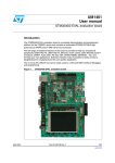
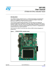
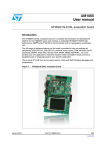
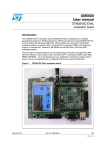
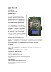
UMxxxx
User Manual
STM3220F-EVAL
Evaluation Board
Introduction
Figure 1: STM3220F-EVAL evaluation board
The STM32F207IFT6 evaluation board
STM3220F-EVAL is designed as complete
development platform for STMicroelectronic’s
ARM Cortex-M3 core-based STM32F207IFT6
microcontroller with digital camera module
interface, High speed USB OTG, Full speed
USB OTG, Ethernet MAC, FSMC interface, two
channels of CAN2.0A/B compliant interface, 2
channels I2S, 3 channels I2C, 6 channels
USART with smart card support, 3 channels SPI,
SDIO, 3 ADC, 2 DAC, internal 128KB SRAM
and 1MB Flash, JTAG&SWD debugging
support.
The full range of hardware features on the
board is able to help you evaluate all
peripherals (USB OTG HS, USB OTG FS,
Ethernet, Motor Control, CAN, MicroSD card,
Smart card, USART, Audio DAC, RS232, IrDA,
PSRAM, OneNAND, MEMS, EEPROM… etc.)
and develop your own applications. Extension
headers make it possible to easily connect a
daughter board or wrapping board for your
specific application.
Features
■
■
■
■
■
■
■
■
■
■
■
■
■
■
■
Four 5V power supply options: Power jack, USB FS connector, USB HS connector or
daughter board.
Boot from User Flash, System memory or SRAM.
I2S Audio DAC, stereo audio jack.
1GByte or more MicroSD card.
Both type A&B Smart card support.
I2C compatible serial interface 64KBit EEPROM, MEMS and IO Expander.
RS232 communication.
IrDA transceiver.
USB OTG HS and FS with Micro-AB connector.
IEEE-802.3-2002 compliant Ethernet connector.
Camera module
4Mbit PSRAM
512Mbit OneNAND
Two channels of CAN2.0A/B compliant connection.
Inductor Motor Control connector.
STM3220F-EVAL Board
■
■
■
■
■
■
■
■
JTAG ,SW and Trace Debug support.
3.2” 240x320 TFT color LCD with touch screen.
Joystick with 4-direction control and selector.
Reset, Wakeup, Tamper and User button.
4 color LEDs.
RTC with backup battery.
MCU consumption measurement circuit
Extension connector for daughter board or wrapping board.
Qing SHAO
Page 2
03/06/2009
STM3220F-EVAL Board
Contents
1. Hardware Layout and configuration ...................................................................................... 4
1.1 Power Supply .................................................................................................................. 6
1.2 Boot Option ..................................................................................................................... 7
1.3 Clock Source ................................................................................................................... 8
1.4 Reset Source................................................................................................................... 8
1.5 Audio ............................................................................................................................... 8
1.6 EEPROM......................................................................................................................... 8
1.7 CAN ................................................................................................................................. 8
1.8 RS232 & IrDA................................................................................................................ 10
1.9 Motor Control................................................................................................................. 10
1.10 Smart Card .................................................................................................................. 11
1.11 MicroSD card............................................................................................................... 12
1.12 MEMS.......................................................................................................................... 12
1.13 Analog Input ................................................................................................................ 12
1.14 USB OTG FS............................................................................................................... 13
1.15 Ethernet....................................................................................................................... 13
1.16 USB OTG HS .............................................................................................................. 14
1.17 Camera Module........................................................................................................... 14
1.18 PSRAM and OneNAND .............................................................................................. 14
1.19 Development and Debug support ............................................................................... 14
1.20 Display and Input devices ........................................................................................... 14
1.21 IDD measurement and comparator............................................................................. 15
2. Connector ............................................................................................................................ 17
2.1 Daughter board extension connector CN1,2,3 and CN4 .............................................. 17
2.2 Motor control connector CN5 ........................................................................................ 21
2.3 MicroSD connector CN6 ............................................................................................... 22
2.4 Ethernet RJ45 connector CN7 ...................................................................................... 22
2.5 USB OTG FS Micro-AB connector CN8 ....................................................................... 23
2.6 USB OTG HS Micro-AB connector CN9 ....................................................................... 23
2.7 CAN D-type 9-pins male connector CN10(CAN2) & CN12(CAN1) .............................. 24
2.8 Audio connector CN11 .................................................................................................. 24
2.9 Trace debugging connector CN13 ................................................................................ 24
2.10 JTAG debugging connector CN14 .............................................................................. 25
2.11 Camera module connector CN15................................................................................ 25
2.12 RS232 connector CN16 .............................................................................................. 26
2.13 Analog input connector CN17 ..................................................................................... 26
2.14 Power connector CN18 ............................................................................................... 26
2.15 TFT LCD connector CN19 .......................................................................................... 27
2.16 Smart card connector CN20........................................................................................ 27
3. Known limitations and bugs on PCB rev A.......................................................................... 28
4. Schematic ............................................................................................................................ 29
Appendix A STM3220F-EVAL IO Assignment ........................................................................ 49
Appendix B Document Revision History.................................................................................. 53
Qing SHAO
Page 3
03/06/2009
STM3220F-EVAL Board
1. Hardware Layout and configuration
The STM3220F-EVAL evaluation board is designed around the STM32F207IFT6 in 176-pin
TQFP package. The hardware block diagram Figure 2 illustrates the connection between
STM32F207IFT6 and peripherals (Camera module, LCD, PSRAM, OneNAND, EEPROM,
MEMS, USART, IrDA, USB OTG HS, USB OTG FS, Ethernet, Audio, CAN bus, Smart card,
MicroSD card and Motor Control) and Figure 3 will help you locate these features on the
actual evaluation board.
Figure 2: Hardware Block Diagram
1.8V regulator
USB power
switch
2.5V regulator
OTG HS
USB HS
PHY
USBMicro-AB
connector
2.8V regulator
DAC
3.3V regulator
I2S2
MCU
consumption
measurement
Audio DAC
I2C1
MEMS
EEPROM
Joystick
LEDs,Key
GPIO
IO expandor
Touchscreen
Extension
connector for
GPIOs
STM32F207IFT6
DCMI
Camera
module
OneNAND
PSRAM
FSMC
USB power
switch
TFT LCD
MicroSD
card
SDIO
MC control
connector
MC
MII/RMII
CAN
DB9 connector
CAN2
CAN
transceiver
CAN
DB9 connector
RS232
transceiver
RS232
DB9 connector
USART3
IrDA
transceiver
ADC
USART6
Potentiometer
Qing SHAO
Integrated RJ45
connector
CAN
transceiver
Debug
Trace
PHY
CAN1
JTAG/SWD
BNC connector
USB Micro-AB
connector
OTG FS
Page 4
Smart Card
interface
Smart Card
connector
03/06/2009
STM3220F-EVAL Board
Figure 3: STM3220F-EVAL Evaluation board layout
CN17
Motor control
CN1-CN4
Extension header
CN6
MicroSD
card
CN7
RJ45
connector
CN8
USB OTG FS
U16
STM32F207IFT6
CN9
USB OTG HS
CN10
CAN2
U11
IrDA
CN11
Audio Jack
CN12
CAN1
CN13
Trace
CN14
JTAG
CN16
USART3
CN19
Color LCD
CN15
Camera module
CN17
BNC connector
CN18
5V power jack
RV1
Potentiometer
B4
User Key
B1
RESET
B2
WAKEUP
Qing SHAO
U32
Joystick
B3
Tamper
CN20
Smartcard
Page 5
03/06/2009
STM3220F-EVAL Board
1.1 Power Supply
STM3220F-EVAL evaluation board is designed to be powered by 5V DC power supply and to
be protected by PolyZen from wrong power plug-in event. It’s possible to configure the
evaluation board to use any of following Four sources for the power supply.
■
■
■
■
5V DC power adapter connected to CN18, the Power Jack on the board (PSU on silk
screen for Power Supply Unit).
5V DC power with 500mA limitation from CN8, the USB OTG FS Micro-AB connector
(FS on silkscreen).
5V DC power with 500mA limitation from CN9, the USB OTG HS Micro-AB connector
(HS on silkscreen).
5V DC power from both CN1 and CN3, the extension connector for daughter board
(DTB for Daughter Board on silkscreen).
The power supply is configured by setting the related jumpers JP17, JP18 & JP19 as
described in table 1.
Table 1 Power related Jumpers
Jumper
JP17
Description
JP17 is used to measure MCU current consumption manually by multimeter.
Default setting: Fitted
JP18 is used to select one of the four possible power supply resources.
JP18
For power supply jack(CN18) to the STM3220F-EVAL only, JP18 is set
as shown to the right:
(Default Setting)
HS
FS
DTB
PSU
For power supply from the daughter board connectors(CN1 and CN3) to
STM3220F-EVAL only, JP18 is set as shown to the right:
HS
FS
DTB
PSU
For power supply from USB OTG FS (CN8) to STM3220F-EVAL only,
JP18 is set as shown to the right:
HS
FS
DTB
PSU
For power supply from USB OTG HS (CN9) to STM3220F-EVAL only,
JP18 is set as shown to the right:
HS
FS
DTB
PSU
Qing SHAO
Page 6
03/06/2009
STM3220F-EVAL Board
For power supply from power supply jack(CN18) to both STM3220FEVAL and daughter board connected on CN1 and CN3, JP18 is set as
shown to the right (daughter board must not have its own power
supply connected)
HS
FS
DTB
PSU
Vbat is connected to battery when JP19 is set as shown to the right:
1 2 3
JP19
Vbat is connected to 3.3V power when JP19 is set as shown to the right:
(Default setting)
1 2 3
To enable MCU power consumption measurement, JP16 should be re-configured as
described in table 2.
Table 2 MCU Power consumption measurement related Jumpers
JP16 is useded to bypass MCU power consumption measurement circuit,
it’s set to close by default.
JP16
JP16 need to be re-configured to open for MCU power consumption
measurement.
Default setting: Fitted
The LED LD9 is lit when the STM3220F-EVAL evaluation board is powered by the 5V
correctly.
1.2 Boot Option
The STM3220F-EVAL evaluation board is able to boot from:
■
■
■
Embedded User Flash
System memory with boot loader for ISP
Embedded SRAM for debugging
The boot option is configured by setting switch SW1 (BOOT1) and SW2 (BOOT0). The
BOOT0 can be configured also via RS232 connector CN16.
Table 3 Boot related Switch
Switch
BOOT0 & 1
Boot from
Switch
configuration
STM3220F-EVAL boot from User Flash when BOOT0 is
set as shown to the right. BOOT1 is don’t care in this
configuration.
(Default setting)
STM3220F-EVAL boot from Embedded SRAM when
BOOT0 and BOOT1 are set as shown to the right.
STM3220F-EVAL boot from System Memory when
BOOT0 and BOOT1 are set as shown to the right.
Qing SHAO
Page 7
03/06/2009
STM3220F-EVAL Board
1.3 Clock Source
Four clock sources are available on STM3220F-EVAL evaluation board for STM32F207IFT6
and RTC embedded.
■
■
■
■
X1, 25MHz Crystal for Ethernet PHY.
X2, 24MHz Crystal for USB OTG HS PHY.
X3, 32KHz Crystal for embedded RTC.
X4, 25MHz Crystal with socket for STM32F207IFT6 Microcontroller, it can be
removed from socket when internal RC clock is used.
1.4 Reset Source
The reset signal of STM3220F-EVAL evaluation board is low active and the reset sources
include:
■
■
■
■
Reset button B1
Debugging Tools from JTAG connector CN14 and Trace connector CN13
Daughter board from CN3
RS232 connector CN16 for ISP.
Table 4 Reset Related Jumpers
Jumper
JP25
Description
Enable reset of the STM32F207IFT6 embedded JTAG TAP controller each
time a system reset occurs. JP25 connects the TRST signal from the
JTAG connection with the system reset signal RESET#.
Default Setting: Not fitted
1.5 Audio
STM3220F-EVAL evaluation board supports stereo audio play thanks to an audio DAC
CS43L22 connected to both I2S2 port and one channels of DAC of microcontroller
STM32F207IFT6. The CS43L22 can be configured via I2C1. The automatically switch
between the speaker and headphone is supported by both CS43L22 and audio jack with plug
detection pin.
1.6 EEPROM
A 64KBit EEPROM connected to I2C1 bus of STM32F207IFT6.
Table 5 EEPROM Related Jumpers
Jumper
Description
The EEPROM is in Write protection mode when JP24 is closed.
JP24
Default Setting: Not fitted
1.7 CAN
STM3220F-EVAL evaluation board supports two channels of CAN2.0A/B complaint CAN bus
communication based on 3.3V CAN transceiver. The two CAN bus are disabled and
disconnected by jumpers from relevant STM32F207IFT6 IO’s which are shared with FSMC
and USB OTG HS. The jumper JP14 and JP15 must be re-set to enable CAN1 while JP10
and JP11 must be re-set to enable CAN2 as listed in table 6 and table 7.
The High-speed mode, standby mode and slope control mode are available and can be
selected by setting JP12 for CAN1 and JP7 for CAN2.
Qing SHAO
Page 8
03/06/2009
STM3220F-EVAL Board
Table 6 CAN1 related Jumpers
Jumper
Description
CAN1 transceiver is working in standby mode when JP12 is set as shown
to the right:
1 2 3
JP12
CAN1 transceiver is working in high-speed mode when JP12 is set as
shown to the right: (default setting)
1 2 3
CAN1 transceiver is working in slope control mode when JP12 is open.
CAN1 terminal resistor is enabled when JP13 is fitted.
JP13
JP14
JP15
Default setting: Not fitted
CAN1_TX is connected to PD1 and all peripherals connected to FSMC
(LCD, PSRAM & OneNAND) are disabled when JP14 is closed.
Default setting: Not fitted
CAN1_RX is connected to PD0 and all peripherals connected to FSMC
(LCD, PSRAM & OneNAND) are disabled when JP15 is closed.
Default setting: Not fitted
.
Table 7 CAN2 related Jumpers
Jumper
Description
CAN2 transceiver is working in standby mode when JP7 is set as shown to
the right:
1 2 3
JP7
CAN2 transceiver is working in high-speed mode when JP7 is set as
shown to the right: (default setting)
1 2 3
CAN2 transceiver is working in slope control mode when JP7 is open.
CAN2 terminal resistor is enabled when JP9 is fitted.
JP9
JP10
JP11
Default setting: Not fitted
CAN2_TX is connected to PB13 and USB OTG HS is disabled when JP10
is closed. JP10 must be open for USB OTG HS application.
Default setting: Not fitted
CAN2_RX is connected to PB5 and USB OTG HS is disabled when JP11
is closed. JP11 must be open for USB OTG HS application.
Default setting: Not fitted
Qing SHAO
Page 9
03/06/2009
STM3220F-EVAL Board
1.8 RS232 & IrDA
Both RS232 and IrDA communication is supported by D-type 9-pins RS232 connectors CN16
and IrDA transceiver U11 which are connected to USART3 of STM32F207IFT6 on
STM3220F-EVAL evaluation board. Two signals, Bootloader_BOOT0 and
Bootloader_RESET, are added on RS232 connector for ISP support.
RS232 or IrDA can be selected by setting of JP22:
Table 8 RS232 & IrDA Related Jumpers
Jumper
Description
USART3_RX is connected to IrDA transceiver and IrDA communication is
enabled when JP22 is set as shown to the right:
1 2 3
JP22
USART3_RX is connected to RS232 transceiver and RS232
communication is enabled when JP22 is set as shown to the right(Default
setting):
1 2 3
JP22 must be set to open to enable MicroSD card witch shares same IOs
with RS232.
1.9 Motor Control
STM3220F-EVAL evaluation board supports three-phase brushless motor control via a 34pins connector CN17, which provides all required control and feedback signals to and from
motor power-driving board. Available signals on this connector includes emergency stop,
motor speed, 3 phase motor current, bus voltage, Heatsink temperature coming from the
motor driving board and 6 channels of PWM control signal going to the motor driving circuit.
JP2 allows to choose two kind to synchronization methods for PFCs (Power Factor
Correction).
The I/O pins used on Motor control connector CN17 are multiplexed with some peripherals on
the board; either motor control connector or multiplexed peripherals can be enabled by setting
of jumpers JP4, JP20 and JP3:
Table 9 Motor Control Related Jumpers
Qing SHAO
Page 10
03/06/2009
STM3220F-EVAL Board
Jumper
JP2
Description
JP2 allows to have a PFC synchronization signal redirected to the timer 3
input capture 2 pin, additionally to the timer3 external trigger input.
Default setting: Not Fitted
JP1 should be kept on open when encoder signal is input from pin31 of
CN5 while it should be kept on close when analog signal is from pin31 of
CN5 for special motor.
JP1
SB3
Default setting: Not Fitted
Solder bridge SB3 is closed by default to connect BNC connector and
Motor control connector to PF8. For external analog input connected to
TP3 and TP4, SB3 may be disconnected. It allows to connect an analogue
source to ADC for accuracy and reliability evaluation with minimum noise
induced by components on the board.
Default setting: close
Jumper
Multiplexed
peripherals
Description
MC_BusVoltage is connected to PF6 when JP20 is set as
shown to the right:
1 2 3
JP20
SmartCard_OFF is connected to PF6 when JP20 is set as
show to the right (Default setting):
Smart card
1 2 3
MC_HeatsinkTemperature is connected to PF7 when JP3 is
closed. JP3 must be open for Smart card.
JP3
Default setting: Not Fitted
MC_EmergencySTOP is connected to PI4 when JP4 is
closed.
JP4
Default setting: Not Fitted
Note: MicroSD card must be removed from CN6 for Motor control application.
Camera
module
connected
to CN15
1.10 Smart Card
STMicroelectronics Smart card interface chip ST8024 is used on STM3220F-EVAL board for
asynchronous 3V and 5V smart cards. It performs all supply protection and control functions
based on the connections with STM32F207IFT6 listed in table 10:
Table 10 Connection between ST8024 and STM32F207IFT6
Signals of
ST8024
5V/3V
I/OUC
XTAL1
OFF
RSTIN
CMDVCC
Qing SHAO
Description
Smart card power supply selection pin.
MCU data I/O line
Crystal or external clock input
Detect presence of a card, Interrupt to MCU, share same
pin with Motor controller
Card Reset Input from MCU
Start activation sequence input (Active Low), share same pin
with I2S DAC and Motor control
Page 11
Connect to
STM32F207IFT6
PH15
PC6
PG7
PF6
PF7
PG12
03/06/2009
STM3220F-EVAL Board
Smart card shares some IO’s with Motor control connector CN5 and I2S bus for Audio.
Some jumper has to be re-configured to enable Smartcard as listed below:
Table 11 Smartcard Related Jumpers
Jumper
Description
SmartCard_IO is connected to PC6 when JP21 is closed. JP21 must be
open for Audio DAC connected to I2S.
JP21
JP3 & JP20
Default setting: Not Fitted
Description of JP3 and JP20 is in chapter 1.9 Motor control.
1.11 MicroSD card
The 1GByte or more MicroSD card connected to SDIO of STM32F207IFT6 is available on the
board. MicroSD card Detection is managed by standard IO port PH13. MicroSD card shares
same IO’s with Motor control & RS232. The jumper JP22 must be open and Motor control
connector (CN6) must be disconnected for MicroSD card.
Table 12 MicroSD card related Jumpers
Jumper
JP22
Description
Description of JP22 is in chapter 1.8 RS232 & IrDA.
1.12 MEMS
A ST MEMS device LIS302DL is connected to I2C1 bus of STM32F207IFT6 on the board.
1.13 Analog Input
One BNC connectors CN17 is connected to PF8 of STM32F207IFT6 as external analog input
when Motor control connector is not used. The 50 ohm terminal resistor can be enabled by
closing of solder bridge SB8. A low pass filter can be implemented for BNC connector by
replacing of R74 and C59 with right value of resister and capacitor as requested by end user’s
application.
Note: For ADC accuracy measurement please use TP3 & TP4 as described in table 9 on
chapter 1.9
There are also 2 analog signals available on the board:
1. 10K ohm potentiometer RV1 connected to PC2 via jumper JP23.
2. IDD measurement output signal connected to PF9 for power consumption test in RUN,
SLEEP and STOP mode.
Table 13 Potentiometer related Jumpers
Jumper
JP23
Description
Potentiometer RV1 is connected to PC2 when JP23 is closed. JP23 must
be open for Ethernet application.
Default setting: Not fitted
The 50ohm terminal resistor is enabled when SB8 is closed.
SB8
Default setting: open
Qing SHAO
Page 12
03/06/2009
STM3220F-EVAL Board
1.14 USB OTG FS
STM3220F-EVAL evaluation board support USB OTG full speed communication via a USB
Micro-AB connector (CN8) and USB power switch (U1) connected to VBUS. The evaluation
board can be powered by this USB connection at 5V DC with 500mA current limitation.
The LED LD6 will be light when power switch (U1) is ON and STM3220F-EVAL works as a
USB host or if VBUS is powered by another USB host when STM3220F-EVAL works as a
USB device. The LD5 will be light when over-current is occurred.
1.15 Ethernet
STM3220F-EVAL evaluation board support 10M/100M Ethernet communication by a PHY
DP83848CVV (U5) and integrated RJ45 connector (CN7). Both MII and RMII interface mode
are supported and can be selected by setting of jumpers JP5, JP6 and JP8 as listed below:
Table 14 Ethernet Related Jumpers and solder bridges
Jumper
Description
JP8 is used to select MII or RMII interface mode. MII is enabled when JP8
is open while RMII interface mode is enabled when JP8 is close.
JP8
Default setting: Not Fitted
JP6 should be set as shown to the right when MII interface mode is
enabled(Default setting):
1 2 3
JP6
JP6 should be set as shown to the right when RMII interface mode is
enabled:
1 2 3
25MHz clock for MII or 50MHz clock for RMII is provided by MCO at PA8
when JP5 is set as shown to the right (Default setting):
1 2 3
JP5
25MHz clock is provided by external crystal X1 (for MII interface mode
only) when JP5 is set as shown to the right:
1 2 3
JP23
SB1
SB2
JP5 has to be kept open when clock is provided by external oscillator U3
(not fit by default)
Description of JP23 is in chapter 1.13 Analog Input.
SB1 is used to select clock source only for RMII mode, the clock from
MCO is connected to RMII_REF_CLK when SB1 is closed.
Default setting: open
SB2 is used to select clock source only for RMII mode, the clock from
pin25 of Ethernet PHY U5 is connected to RMII_REF_CLK when SB2 is
closed.
Default setting: close
A tes tpoint TP2 is available on the board for PTP_PPS feature test, it can be used only when
JP11 is kept on open. (Note: there are no problem of conflict between PTP_PPS output &
ULPI data bus, pls. refer to 6.1.9.3 interface protection of USB3300. TBC)
Qing SHAO
Page 13
03/06/2009
STM3220F-EVAL Board
1.16 USB OTG HS
STM3220F-EVAL evaluation board support USB OTG High speed communication via a USB
Micro-AB connector (CN9), USB High speed PHY (U8) and USB power switch (U4)
connected to VBUS. The evaluation board can be powered by this USB connector (CN9) at
5V DC with 500mA current limitation.
The LED LD7 will be light when power switch (U4) is ON and STM3220F-EVAL works as a
USB host or if VBUS is powered by another USB host when STM3220F-EVAL works as a
USB device. The LD8 will be light when over-current is occurred.
The USB ULPI bus is shared with CAN2 bus, the JP10 and JP11 must be kept on open for
USB OTG HS.
1.17 Camera Module
A 1.3Mega Pixel camera module is connected to DCMI bus of STM32F207IFT6 and shares
same IOs with motor control connector. JP4 must be kept on open for Camera module
application.
Table 15 Camera module Related Jumpers
Jumper
Description
The camera module is in power down mode when JP26 is closed.
JP26
Default setting: Not Fitted
JP4
Description of JP4 is in chapter 1.9 Motor control.
1.18 PSRAM and OneNAND
The 4Mbit PSRAM and 512Mbit OneNAND are connected to FSMC bus of STM32F207IFT6
which shares same IO’s with CAN1 bus. The JP14 and JP15 must be kept on open for
PSRAM, OneNAND and LCD application.
1.19 Development and Debug support
The two debug connectors available on STM3220F-EVAL evaluation board are:
1. CN14, standard 20-pins JTAG interface connector that is compliant with debug tools of
ARM7 and ARM9.
2. CN13, SAMTEC 20-pins connector FTSH-110-01-L-DV for both SWD and Trace that is
compliant with ARM CoreSight debug tools.
1.20 Display and Input devices
The 3.2” TFT color LCD connected to FSMC bus and 4 general purpose color LED’s (LD
1,2,3,4) are available as display device. A touch screen connected to IO expander (U24), 4direction joystick with selection key, general purpose button (B4), Wakeup button (B2) and
Tamper detection button (B3) are available as input devices.
Table 16 LCD modules
Pin on
CN16
1
2
3
4
5
6
7
8
Pin name
CS
RS
WR/SCL
RD
RESET
PD1
PD2
PD3
Qing SHAO
3.2” TFT LCD with touch screen (CN16)
Pin connection
Pin on
Pin name
CN16
FSMC_NE3 (PG10)
18
PD14
FSMC_A0
19
PD14
FSMC_NWE
20
PD16
FSMC_NOE
21
PD17
RESET#
22
BL_GND
FSMC_D0
23
BL_Control
FSMC_D1
24
VDD
FSMC_D2
25
VCI
Page 14
Pin connection
FSMC_D12
FSMC_D13
FSMC_D14
FSMC_D15
GND
+5V
+3V3
+3V3
03/06/2009
STM3220F-EVAL Board
9
10
11
12
13
14
PD4
PD5
PD6
PD7
PD8
PD10
FSMC_D3
FSMC_D4
FSMC_D5
FSMC_D6
FSMC_D7
FSMC_D8
26
27
28
29
30
31
GND
GND
BL_VDD
SDO
SDI
XL
15
PD11
FSMC_D9
32
XR
16
PD12
FSMC_D10
33
YD
17
PD13
FSMC_D11
34
YU
GND
GND
+5V
NC
NC
IO expander
U24
IO expander
U24
IO expander
U24
IO expander
U24
1.21 IDD measurement and comparator
For IDD measurement the circuit below is implemented on STM3220F-EVAL.
Figure 4: STM3220F-EVAL IDD measurement circuit
In Run mode, IDD current is measured thanks to TSC101BILT (U14) connected to the 1ohm
shunt resistor. In this case IDD_CNT_EN remains at high level during measurement and
JP16 jumper must be removed.
In Halt mode, the operational amplifier TSC101BILT (U14) is connected on the 1Kohm shunt
resistor. To measure a current corresponding to the Halt mode the procedure is:
1. Configure ADC to measure voltage on IDD_measurement pin.
2. Configure PA0 as interrupt input on falling edge
3. Enter in Halt or active Halt mode with IDD_CNT_EN Low
4. LP_WAKEUP falling edge wakeup the MCU after 100ms
5. start ADC conversion as soon as possible after wakeup in order to measure the
voltage corresponding to Sleep mode on 1uF capacitor
6. Reset the counter by programming IDD_CNT_EN High in less than 50mS after
the wakeup to avoid 1Kohm to be connected later on VDD_MCU
In Halt mode, the 1K resistor is connected when T1 become off after entering in Halt mode.
Q13 output of the counter allows connecting the 1K when the current IDD becomes very low.
The measurement timing is given below:
Figure 5: STM3220F-EVAL IDD Halt mode measurement timing diagram
Qing SHAO
Page 15
03/06/2009
STM3220F-EVAL Board
Halt mode IDD measurement timing
Run
W ake-up
ID D Measu re
C lear C N T
H alt
MC U mo de
0
150mS
300mS
450mS
ID D_C N T_EN (PI8)
Q13= L OW _POW ER _EN
(T1 p in 3)
Q14 = L P_W AK EU P
(PA0)
Q14n = Switch
co ntro l (U 15 p in 4)
The halt mode measurement procedure can be used in Halt mode and slow or fast active Halt
modes if the IDD current do not exceed 60uA else the Run measurement procedure need to
be used up to 60mA.
Qing SHAO
Page 16
03/06/2009
STM3220F-EVAL Board
2. Connector
2.1 Daughter board extension connector CN1,2,3 and CN4
Four male headers CN1,2,3 and CN4 can be used to connect with daughter board or
standard wrapping board to STM3220F-EVAL evaluation board. All total 140 GPI/Os are
available on it.
Each pin on CN1,2,3 and CN4 can be used by a daughter board after disconnecting it from
the corresponding function block on STM3220F-EVAL evaluation board. Please refer to table
17 to table 20 for detail.
Table 17 Daughter board extension connector CN1
Pin
Description
Alternative
How to disconnect with function block
Function
on STM3220F-EVAL board
1
GND
3
PE3
Trace_D0
5
PE5
Trace_D2
7
PI8
IDD_CNT_EN
9
PC14
OSC32_IN
SB4 open
11
PC15
OSC32_OUT
SB5 open
13
PI10
MII_RX_ER
Remove RS3
15
PF0
FSMC_A0
17
PF2
FSMC_A2
19
GND
21
PF5
FSMC_A5
23
PF7
SmartCard_RS JP3 open
T &MC
25
PF9
IDD_Measure
Remove R82
ment & MC
Disconnect Motor Control board from CN5
27
PH0
OSC_IN
SB6 open
29
PC0
ULPI_STP
31
PC1
MII_MDC
33
PC3
MII_TX_CLK
Remove RS5
35
PA0
WakeUP
Remove R139
37
PA2
MII_MDIO
39
GND
41
PH4
ULPI_NXT
Can not be used on daughter board
43
NC
45
NC
47
EMU_3V3
49
EMU_5V
2
PE2
Trace_CLK
4
PE4
Trace_D1
6
PE6
Trace_D3
8
PC13
Anti-Tamper
Remove R143
10
GND
12
PI9
LED3
Remove R141
14
PI11
ULPI_DIR
Can not be used on daughter board
16
PF1
FSMC_A1
18
PF3
FSMC_A3
20
PF4
FSMC_A4
22
PF6
SmartCard_OF JP20 open
F & MC
24
PF8
MC
Disconnect Motor Control board from CN5
26
PF10
MC
Disconnect Motor Control board from CN5
28
PH1
OSC_OUT
SB7 open
Qing SHAO
Page 17
03/06/2009
STM3220F-EVAL Board
30
32
GND
PC2
34
36
38
40
42
VREF+
PA1
PH2
PH3
PH5
44
46
48
50
NC
NC
APP_3V3
GND
MII_TXD2 &
potentiometer
MII_RX_CLK
MII_CRS
MII_COL
OTG_FS_Pow
erSwitchOn
-
JP23 open
JP6 open
Remove RS3
Remove RS3
Remove R18
-
Table 18 Daughter board extension connector CN2
Pin
Description
Alternative
How to disconnect with function block
Function
on STM3220F-EVAL board
1
GND
3
PA3
ULPI_D0
5
PA5
ULPI_CLK
Can not be used on daughter board
7
PA7
MII_RX_DV
Remove RS2, JP8 open
9
PC5
MII_RXD1
Remove RS2
11
PB0
ULPI_D1
13
PB2
BOOT1
15
PF12
FSMC_A6
17
PF14
FSMC_A8
19
GND
21
PG1
FSMC_A11
23
PE8
FSMC_D5
25
PE10
FSMC_D7
27
PE12
FSMC_D9
29
PE14
FSMC_D11
31
PE15
FSMC_D12
33
PB11
ULPI_D4
35
PH7
MII_RXD3
Remove RS3
37
PH9
DCMI_D0
Remove camera module from CN15
39
GND
2
APP_VCC
4
PA4
Audio_DAC_O Remove R115
UT
6
PA6
DCMI_PIXCK
Remove camera module from CN15
8
PC4
MII_RXD0
Remove RS2
10
GND
12
PB1
ULPI_D2
14
PF11
OTG_FS_Over Remove R15
current
16
PF13
FSMC_A7
18
PF15
FSMC_A9
20
PG0
FSMC_A10
22
PE7
FSMC_D4
24
PE9
FSMC_D6
26
PE11
FSMC_D8
28
PE13
FSMC_D10
30
GND
32
PB10
ULPI_D3
34
PH6
MII_RXD2
Remove RS5
36
PH8
DCMI_HSYNC Remove camera module from CN15
& MC
Disconnect Motor Control board from CN5
38
PH10
DCMI_D1 &MC Remove camera module from CN15
Qing SHAO
Page 18
03/06/2009
STM3220F-EVAL Board
40
PH11
DCMI_D2 &MC
Disconnect Motor Control board from CN5
Remove camera module from CN15
Disconnect Motor Control board from CN5
Table 19 Daughter board extension connector CN3
Pin
Description
Alternative
How to disconnect with function block
Function
on STM3220F-EVAL board
1
GND
3
PI1
I2S_CK
5
PH15
SmartCard_3/5 Disconnect Motor Control board from CN5
V & MC
7
PH13
MicroSDCard_ Remove MicroSD card from CN6
defect & MC
Disconnect Motor Control board from CN5
9
PC13
Anti-Tamper
Remove R143
11
RESET#
Reset button
13
PA11
OTG_FS_DM
Remove R17
15
PA9
VBUS_FS
Remove USB cable from CN8
Remove R18
17
PC9
MicroSDCard_ Remove MicroSD card from CN6
D1 & MC
Disconnect Motor Control board from CN5
19
EMU_5V
21
PC6
I2S_MCK &
JP21 open
SmartCard_IO
23
PG7
SmartCard_CL K
25
PG5
FSMC_A15
27
PG3
FSMC_A13
29
PD15
FSMC_D1
31
PD14
FSMC_D0
33
PD12
FSMC_A17
35
PD10
FSMC_D15
37
PD8
FSMC_D13
39
GND
41
PB13
ULPI_D6 &
CAN2_TX
43
PH12
DCMI_D3 &
Remove camera module from CN15
MC
Disconnect Motor Control board from CN5
45
NC
47
EMU_3V3
49
EMU_5V
2
PI2
IO_Expandor_I Remove R136
NT
4
PI0
I2S_CMD
6
PH14
DCMI_D4 &
Remove camera module from CN15
MC
Disconnect Motor Control board from CN5
8
PA13
TMS/SWDIO
10
GND
12
PA12
OTG_FS_DP
Remove R19
14
PA10
OTG_FS_ID
Remove R21
16
PA8
MCO
JP5 open
18
PC8
MicroSDCard_ Remove MicroSD card from CN6
D0 & MC
Disconnect Motor Control board from CN5
20
PC7
LED4
Remove R140
22
PG8
LED2
Remove R154
24
PG6
LED1
Remove R155
26
PG4
FSMC_A14
28
PG2
FSMC_A12
30
GND
-
Qing SHAO
Page 19
03/06/2009
STM3220F-EVAL Board
32
34
36
38
40
42
44
46
48
50
PD13
PD11
PD9
PB15
PB14
PB12
NC
NC
APP_3V3
GND
MC
FSMC_A16
FSMC_D14
OneNAND_INT
MII_INT
ULPI_D5
-
Disconnect Motor Control board from CN5
Remove R53
Remove R41
-
Table 20 Daughter board extension connector CN4
Pin
Description
Alternative
How to disconnect with function block
Function
on STM3220F-EVAL board
1
GND
3
PI6
DCMI_D6 &
Remove camera module from CN15
MC
Disconnect Motor Control board from CN5
5
PI4
DCMI_D5 &
Remove camera module from CN15
MC
JP4 open
7
PE0
FSMC_BL0
9
PB8
MII_TXD3 &
Remove RS5
MC
Disconnect Motor Control board from CN5
11
BOOT0
BOOT0
13
PB6
I2C1_SCK
Remove R103
15
PB4
TRST
17
PG15
User button
Remove R150
19
GND
21
PG12
SmartCard_C
Remove R128
MDVCC
23
PG10
FSMC_NE3
Remove LCD board MB785 from CN19
25
PD7
FSMC_NE1
Remove R52
27
PD5
FSMC_NWE
29
PD3
FSMC_CLK
31
PD2
MicroSDCard_ CMD
33
PD0
FSMC_D2 &
JP15 open
CAN1_RX
35
PC11
MicroSDCard_ JP22 open
D3 &
Remove MicroSD card from CN6
RS232/IrDA_R
X
37
PA15
TDI
39
GND
2
PI7
DCMI_D7 &
Remove camera module from CN15
MC
Disconnect Motor Control board from CN5
4
PI5
DCMI_VSYNC Remove camera module from CN15
& MC
Disconnect Motor Control board from CN5
6
PE1
FSMC_BL1
8
PB9
I2C1_SDA
Remove R111
10
GND
12
PB7
FSMC_NL
14
PB5
ULPI_D7 &
JP11 open
CAN2_RX
16
PB3
TDO/SWO
18
PG14
MII_TXD1
Remove RS6
20
PG13
MII_TXD0
Remove RS6
22
PG11
MII_TX_EN
Remove RS6
24
PG9
FSMC_NE2
Remove R47
26
PD6
FSMC_NWAIT Remove R54
Qing SHAO
Page 20
03/06/2009
STM3220F-EVAL Board
28
30
32
PG4
GND
PD1
34
PC12
36
PC10
38
40
PA14
PI3
FSMC_A14
FSMC_D3 &
CAN1_TX
MicroSDCard_
CLK
MicroSDCard_
D2 &
RS232/IrDA_T
X
TCK/SWCLK
I2S_DIN
JP14 open
Remove MicroSD card from CN6
Remove MicroSD card from CN6
-
Note: The 0ohm resister will added on PCB rev.B for PI11(ULPI_DIR), PA5(ULPI_CLK) &
PH4(ULPI_NXT) usage on daughter board. For ULPI[0..7], it’s in input status for PHY
USB3300 by default, so, 0ohm resister is not needed, TBC.
2.2 Motor control connector CN5
Figure 6 Motor Control connector CN5
33 31 29 27 25 23 21 19 17 15 13 11 9 7 5
3
1
34 32 30 28 26 24 22 20 18 16 14 12 10 8 6
4
2
Viewed from above PCB
Table 21 Motor Control connector CN5
PI4
PI5
PH
PI6
PH14
PI7
PH15
3
5
7
9
11
13
4
6
8
10
12
14
PF8
15
16
GND
GND
GND
GND
GND
BUS
VOLTAGE
GND
PF9
17
18
GND
PF10
19
20
GND
PH8
21
22
GND
PC8
23
24
GND
+5V
25
26
EMERGENCY
STOP
PWM-UH
PWM-UL
PWM-VH
PWM-VL
PWM-WH
PWM-WL
Qing SHAO
Description
Pin
number
of CN17
2
Pin of
STM32F207IFT6
PHASE A
CURRENT
PHASE B
CURRENT
PHASE C
CURRENT
NTC BYPASS
RELAY
DISSIPATIVE
BRAKE PWM
+5V power
Pin of
STM32F207IFT6
Pin
number
of CN17
1
Description
Page 21
GND
PF6
PF7
Heatsink
03/06/2009
STM3220F-EVAL Board
PFC SYNC
PFC PWM
Encoder A
Encoder B
PH10 and PH11
PH12
PB8
PD13
27
29
31
33
28
30
32
34
temperature
VDD_Micro
GND
GND
Encoder
Index
PC9
2.3 MicroSD connector CN6
Figure 7 MicroSD connector CN6
Viewed from front
Table 22 MicroSD connector CN6
Pin number
Description
1
2
3
4
SDIO_D2 (PC11)
SDIO_D2 (PC10)
SDIO_CMD (PD2)
+3V3
Pin
number
5
6
7
8
9
Description
SDIO_CLK (PC12)
Vss/GND
SDIO_D0 (PC9)
SDIO_D1 (PC8)
MicroSDcard_detect (PH13)
2.4 Ethernet RJ45 connector CN7
Figure 8 Ethernet RJ45 connector CN7
Viewed from front
Qing SHAO
Page 22
03/06/2009
STM3220F-EVAL Board
Table 23 RJ45 connector CN7
Pin number
Description
1
3
5
7
TxData+
RxData+
Shield
Shield
Pin
number
2
4
6
8
Description
TxDataShield
RxDataShield
2.5 USB OTG FS Micro-AB connector CN8
Figure 9 USB OTG FS Micro-AB connector CN8
Viewed from front
Table 24 USB OTG FS Micro-AB connector CN8
Pin number
1
2
3
Description
VBUS (PA9)
D- (PA11)
D+ (PA12)
Pin number
4
5
Description
ID (PA10)
GND
2.6 USB OTG HS Micro-AB connector CN9
Figure 10 USB OTG HS Micro-AB connector CN9
Viewed from front
Table 25 USB OTG HS Micro-AB connector CN9
Pin number
1
2
3
Qing SHAO
Description
VBUS
DD+
Pin number
4
5
Page 23
Description
ID
GND
03/06/2009
STM3220F-EVAL Board
2.7 CAN D-type 9-pins male connector CN10(CAN2) &
CN12(CAN1)
Figure 11 CAN D-type 9-pins male connector CN10 (CAN2) & CN12 (CAN1)
Viewed from front
Table 26 CAN D-type 9-pins male connector CN10 (CAN2) & CN12 (CAN1)
Pin number
Description
Pin number Description
1,4,8,9
NC
7
CANH
2
CANL
3,5,6
GND
2.8 Audio connector CN11
A 3.5mm Stereo audio jack CN11 with plug-detection feature connected to audio DAC is
available on STM3220F-EVAL board.
2.9 Trace debugging connector CN13
Figure 12 Trace debugging connector CN13
19 17 15 13 11 9 7 5
3
1
20 18 16 14 12 10 8 6
4
2
Viewed from above PCB
Table 27 Trace debugging connector CN13
Pin number
Description
1
3
5
7
9
11
13
15
17
19
Qing SHAO
3.3V power
GND
GND
KEY
GND
GND
GND
GND
GND
GND
Pin
number
2
4
6
8
10
12
14
16
18
20
Page 24
Description
TMS/PA13
TCK/PA14
TDO/PB3
TDI/PA15
RESET#
TraceCLK/PE2
TraceD0/PE3 or SWO/PB3
TraceD1/PE4 or nTRST/PB4
TraceD2/PE5
TraceD3/PE6
03/06/2009
STM3220F-EVAL Board
2.10 JTAG debugging connector CN14
Figure 13 JTAG debugging connector CN14
19 17 15 13 11 9 7 5
3
1
20 18 16 14 12 10 8 6
4
2
Viewed from above PCB
Table 28 JTAG debugging connector CN14
Pin number
Description
1
3
5
7
9
11
13
15
17
19
3.3V power
PB4
PA15
PA13
PA14
RTCK
PB3
RESET#
DBGRQ
DBGACK
Pin
number
2
4
6
8
10
12
14
16
18
20
Description
3.3V power
GND
GND
GND
GND
GND
GND
GND
GND
GND
2.11 Camera module connector CN15
Figure 14 Camera module connector CN15
Viewed from front
Table 29 Camera module connector CN15
Pin number
1
2
3
4
5
6
7
8
9
10
Qing SHAO
Description
DGND
DGND
SIO_D (PB9)
AVDD (2.8V)
SIO_C (PB6)
RESET
VSYNC (PI5)
PWDN
HREF (PH8)
DVDD (1.8V)
Pin number
13
14
15
16
17
18
19
20
21
22
Page 25
Description
XCLK1
Y6(PI6)
DGND
Y5(PI4)
PCLK (PA6)
Y4(PH14)
Y0 (PH9)
Y3(PH12)
Y1(PH10)
Y2(PH11)
03/06/2009
STM3220F-EVAL Board
11
12
VOVDD (2.8V)
Y7(PI7)
23
24
AGND
AGND
2.12 RS232 connector CN16
Figure 15 RS232 connector CN16 with ISP support
Viewed from front
Table 30 RS232 connector CN16 with ISP support
Pin number
Description
Pin
number
1
Bootloader_RESET
6
2
RS232_RX (PC11)
7
3
RS232_TX (PC10)
8
4
NC
9
5
GND
Description
NC
NC
Bootloader_BOOT0
NC
2.13 Analog input connector CN17
Figure 16 Analog input connector CN17
1
1
2
5
4
3
Viewed from bottom
Table 31 Analog input connector CN17
Pin number
Description
1
2
3
GND
GND
GND
Pin
number
4
5
Description
GND
Analog input PF8
2.14 Power connector CN18
Your STM3220F-EVAL evaluation board can be powered from a DC 5V power supply via the
external power supply jack (CN18) shown in Figure17. The central pin of CN18 must be
positive.
Figure 17 Power supply connector CN18
Qing SHAO
Page 26
03/06/2009
STM3220F-EVAL Board
DC +5V
GND
Viewed from front
2.15 TFT LCD connector CN19
One 34-pin male header CN19 is available on the board to connect LCD module board
MB785. Please refer to chapter 1.20 for detail.
2.16 Smart card connector CN20
Figure 18 Smart card connector CN20
1 2 3 4
17 18
5 6 7 8
Viewed from front
Table 32 Smart card connector CN20
Pin
number
1
2
3
4
17
Qing SHAO
Description
VCC
RST
CLK
NC
Detection pin of card presence
Pin
number
5
6
7
8
18
Page 27
Description
GND
NC
I/O
NC
Detection pin of card presence
03/06/2009
STM3220F-EVAL Board
3. Known limitations and bugs on PCB rev A
•
•
•
•
•
When using MB760 adapter to connect the board to the STice some precautions
need to be considered to avoid short-circuits between MB760 PCB and the daughter
boards connectors CN2, CN3 and CN4 pins. An adhesive strip on bottom side of
MB760 used as isolation may be damaged when the MB687 (flexPCB) is plugged on
MB760 J2 connector. To avoid this issue it strongly recommended to connect first the
MB687 to MB760 then to screw MB760 to MCU socket on evaluation board (MB786).
On Mother board (MB786) Sheet 1 & 4 PB6 and PB9 are named respectively
I2C2_SCL and I2C2_SDA. Actually PB6 and PB9 alternate function are on I2C1
DCD signal on RS232 connector is connected to board RESET for bootloader
applications. It is not possible to disconnect this signal from RESET directly on the
board so when using RS232 interface the host need to maintain DCD signal low or
the corresponding pin needs to be disconnected on RS232 cable or connector.
BOOT0 and BOOT1 switches are swapped on the silkscreen.
Joystick is rotated by 180° compared to signals names on the schematic. Therefore a
workaround is needed in the software to swap up with down and right with left signals.
Qing SHAO
Page 28
03/06/2009
STM3220F-EVAL Board
4. Schematic
Qing SHAO
Page 29
03/06/2009
STM3220F-EVAL Board
Qing SHAO
Page 30
03/06/2009
STM3220F-EVAL Board
Qing SHAO
Page 31
03/06/2009
STM3220F-EVAL Board
Qing SHAO
Page 32
03/06/2009
STM3220F-EVAL Board
Qing SHAO
Page 33
03/06/2009
STM3220F-EVAL Board
Qing SHAO
Page 34
03/06/2009
STM3220F-EVAL Board
Qing SHAO
Page 35
03/06/2009
STM3220F-EVAL Board
Qing SHAO
Page 36
03/06/2009
STM3220F-EVAL Board
Qing SHAO
Page 37
03/06/2009
STM3220F-EVAL Board
Qing SHAO
Page 38
03/06/2009
STM3220F-EVAL Board
Qing SHAO
Page 39
03/06/2009
STM3220F-EVAL Board
Qing SHAO
Page 40
03/06/2009
STM3220F-EVAL Board
Qing SHAO
Page 41
03/06/2009
STM3220F-EVAL Board
Qing SHAO
Page 42
03/06/2009
STM3220F-EVAL Board
Qing SHAO
Page 43
03/06/2009
STM3220F-EVAL Board
Qing SHAO
Page 44
03/06/2009
STM3220F-EVAL Board
Qing SHAO
Page 45
03/06/2009
STM3220F-EVAL Board
Qing SHAO
Page 46
03/06/2009
STM3220F-EVAL Board
Qing SHAO
Page 47
03/06/2009
STM3220F-EVAL Board
Qing SHAO
Page 48
03/06/2009
STM3220F-EVAL Board
Pin No.
Appendix A STM3220F-EVAL IO Assignment
1
2
3
4
5
6
7
8
9
10
11
12
13
14
15
16
17
18
19
20
21
22
23
24
25
26
27
28
29
30
31
32
33
34
35
36
37
38
39
40
41
42
43
44
Pin Name
STM3220F-EVAL IO Assignment
PE2
PE3
PE4
PE5
PE6
VBAT
PI8- ANTI
TAMP2
PC13ANTI_TAMP
PC14-OSC32_IN
PC15OSC32_OUT
PI9
PI10
PI11
VSS_13
VDD_13
PF0
PF1
PF2
PF3
PF4
PF5
VSS_5
VDD_5
PF6
PF7
PF8
PF9
PF10
PH0 - OSC_IN
PH1 - OSC_OUT
NRST
PC0
PC1
PC2
PC3
VDD_12
VSSA
VREF+
VDDA
PA0-WKUP
PA1
PA2
PH2
PH3
TRACE_CLK / FSMC_A23
TRACE_D0 / FSMC_A19
TRACE_D1 / FSMC_A20
TRACE_D2 / FSMC_A21
TRACE_D3 / FSMC_A22
VBAT
Qing SHAO
IDD_CNT_EN
ANTI-TAMPER_BUTTON
32K_OSC
32K_OSC
LED2
ETHER_RX_ER
USB_HS_DIR
FSMC_A0
FSMC_A1
FSMC_A2
FSMC_A3
FSMC_A4
FSMC_A5
MC_ADC3_4 pin 14 (Busvoltage) / SmartCard_OFF
MC_ADC3_4 pin 26 (Heatsinktemp) / SmartCard_RESET
MC_ADC3_6 pin 15 (Current A) / BNC
MC_ADC3_7 pin 17 (Current B) / ADC13_IDD_Measure
MC_ADC3_8 pin 19 (Current C)
OSC_IN
OSC_OUT
RESET_BUTTON
USB_HS_STP
ETHER_MDC
ETHER_TXD2 / POTENTIOMETER
ETHER_TX_CLK
WAKEUP_BUTTON
ETHER_RX_CLK
ETHER_MDIO
ETHER_CRS
ETHER_COL
Page 49
03/06/2009
STM3220F-EVAL Board
45
46
47
48
49
50
51
52
53
54
55
56
57
58
59
60
61
62
63
64
65
66
67
68
69
70
71
72
73
74
75
76
77
78
79
80
81
82
83
84
85
86
87
88
89
90
91
92
93
94
95
96
97
98
99
Qing SHAO
PH4
PH5
PA3
VSS_4
VDD_4
PA4
PA5
PA6
PA7
PC4
PC5
PB0
PB1
PB2
PF11
PF12
VSS6
VDD_6
PF13
PF14
PF15
PG0
PG1
PE7
PE8
PE9
VSS_7
VDD_7
PE10
PE11
PE12
PE13
PE14
PE15
PB10
PB11
VCAP1
VDD_1
PH6
PH7
PH8
PH9
PH10
PH11
PH12
VSS_14
VDD_14
PB12
PB13
PB14
PB15
PD8
PD9
PD10
PD11
USB_HS_NXT
USB_FS_POWER_ON
USB_HS_D0
Audio_DAC_OUT
USB_HS_CK
CAM_PIXCK
ETHER_DV
ETHER_RXD0
ETHER_RXD1
USB_HS_D1
USB_HS_D2
BOOT1 /
USB_FS_OVERCURRENT
FSMC_A6
FSMC_A7
FSMC_A8
FSMC_A9
FSMC_A10
FSMC_A11
FSMC_D4
FSMC_D5
FSMC_D6
FSMC_D7
FSMC_D8
FSMC_D9
FSMC_D10
FSMC_D11
FSMC_D12
USB_HS_D3
ULPI_D4
ETHER_RXD2
ETHER_RXD3
CAM_HSYNC / MC_NTC_bypass
CAM_D0
CAM_D1 / MC_TIM5_ETR pin 27 (PFC SYNC)
CAM_D2 / MC_TIM3_CH2 pin 27 (PFCSYNC)
CAM_D3 / TIM5_CH3 pin 29 (PFCPWM)
ULPI_D5
ULPI_D6 / CAN2_TX
ETHER_INT
OneNAND_INT
FSMC_D13
FSMC_D14
FSMC_D15
FSMC_A16
Page 50
03/06/2009
STM3220F-EVAL Board
100
101
102
103
104
105
106
107
108
109
110
111
112
113
114
115
116
117
118
119
120
121
122
123
124
125
126
127
128
129
130
131
132
133
134
135
136
137
138
139
140
141
142
143
144
145
146
147
148
149
150
151
152
153
154
Qing SHAO
PD12
PD13
VSS_8
VDD_8
PD14
PD15
PG2
PG3
PG4
PG5
PG6
PG7
PG8
VSS_9
VDD_9
PC6
PC7
PC8
PC9
PA8
PA9
PA10
PA11
PA12
PA13
VCAP2
VSS 2
VDD_2
PH13
PH14
PH15
PI0
PI1
PI2
PI3
VSS_15
VDD_15
PA14
PA15
PC10
PC11
PC12
PD0
PD1
PD2
PD3
PD4
PD5
VSS_10
VDD_10
PD6
PD7
PG9
PG10
PG11
FSMC_A17
MC_TIM4_CH2 pin 33 (EnB)
FSMC_D0
FSMC_D1
FSMC_A12
FSMC_A13
FSMC_A14
FSMC_A15
LED0
SmartCard_CK
LED1
SmartCard_IO / Audio_I2S_ MCK
LED3
SDIO_D0/ MC_TIM3_CH3 pin23 (Dissipative Brake)
SDIO_D1 / MC_TIM5_CH3 pin 34 (Index)
MCO
USB_FS_VBUS
USB_FS_ID
USB_FS_DM
USB_FS_DP
JTAG_TMS
MC_TIM8_CH1N pin 5 (UL) / Usdcard detect
CAM_D4 / MC_TIM8_CH2N pin 9 (VL)
MC_TIM8_CH3N pin 13 (WL) / SmartCard_3/5V
Audio_I2S_WS
Audio_I2S_CK
Expander_INT
Audio_I2S_DOUT
JTAG_TCK
JTAG_TDI
SDIO_D2 / RS232_TX
SDIO_D3 / RS232_RX
SDIO_CK
FSMC_D2 / CAN1_RX
FSMC_D3 / CAN1_TX
SDIO_CMD
FSMC_CLK
FSMC_NOE
FSMC_NWE
FSMC_NWAIT
FSMC_NE1
FSMC_NE2
FSMC_NE3
ETHER_TXEN
Page 51
03/06/2009
STM3220F-EVAL Board
155
156
157
158
159
160
161
162
163
164
165
166
167
168
169
170
171
172
173
174
175
176
Qing SHAO
PG12
PG13
PG14
VSS_11
VDD_11
PG15
PB3
PB4
PB5
PB6
PB7
BOOT0
PB8
PB9
PE0
PE1
VSS_3
VDD_3
PI4
PI5
PI6
PI7
SmartCard_CMDVCC
ETHER_TXD0
ETHER_TXD1
USER_BUTTON
JTAG_TDO
JTAG_TRST
CAN2_RX / ETHER_PPS_OUT / ULPI_D7
I2C1_SCL
FSMC_NL
BOOT0
ETHER_TXD3 / MC_TIM4_CH3 pin 31 (EnA)
I2C1_SDA
FSMC_NBL0
FSMC_NBL1
CAM_D5 / MC_TIM8_BKIN pin 1 (Stop)
CAM_VSYNC / MC_TIM8_CH1 pin 3 (UH)
CAM_D6 / MC_TIM8_CH2 pin 7 (VH)
CAM_D7 / MC_TIM8_CH3 pin 11 (WH)
Page 52
03/06/2009
STM3220F-EVAL Board
Appendix B Document Revision History
Table Document Revision History
Date
Version
09,Apr.2009
0.1
0.2
28,May.2009
Qing SHAO
Revision Details
First version
Updated after review and completed with PCB rev A known
limitations
Page 53
03/06/2009
STM3220F-EVAL Board
Information furnished is believed to be accurate and reliable. However, STMicroelectronics assumes no responsibility for the
consequences of use of such information nor for any infringement of patents or other rights of third parties which may result
from its use. No license is granted by implication or otherwise under any patent or patent rights of STMicroelectronics.
Specifications mentioned in this publication are subject to change without notice. This publication supersedes and replaces
all information previously supplied. STMicroelectronics products are not authorized for use as critical components in life
support devices or systems without express written approval of STMicroelectronics.
The ST logo is a registered trademark of STMicroelectronics.
All other names are the property of their respective owners.
© 2004 STMicroelectronics - All rights reserved
STMicroelectronics GROUP OF COMPANIES
Australia - Belgium - Brazil - Canada - China - Czech Republic - Finland - France - Germany Hong Kong - India - Israel - Italy - Japan - Malaysia - Malta - Morocco - Singapore Spain - Sweden - Switzerland - United Kingdom - United States
www.st.com
Qing SHAO
Page 54
03/06/2009