1
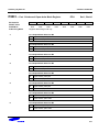
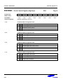
CONTROL REGISTERS
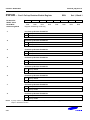
S3F84YB_UM_REV1.00
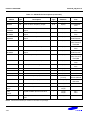
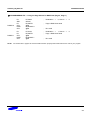
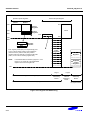
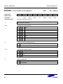
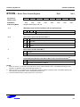
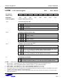
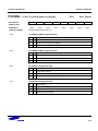
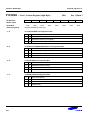
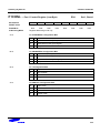
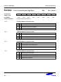
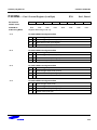
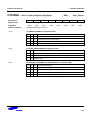
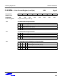
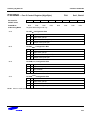
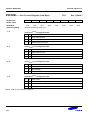
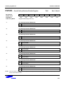
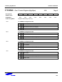
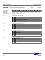
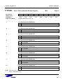
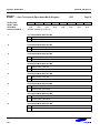
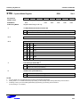
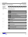
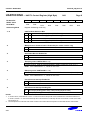
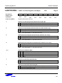
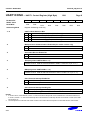
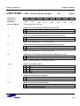
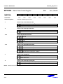
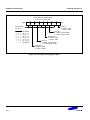
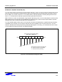
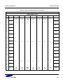
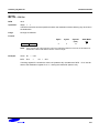
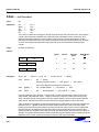
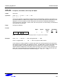
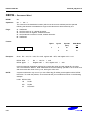
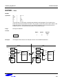
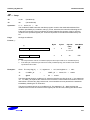
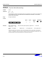
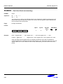
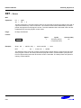
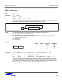
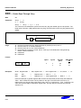
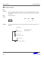
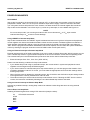
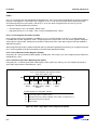
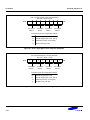
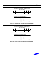
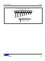
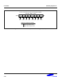
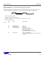
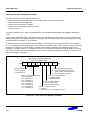
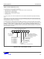
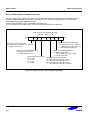
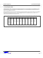
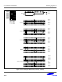
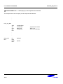
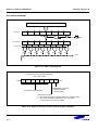
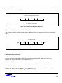
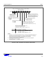
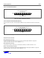
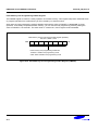
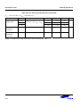
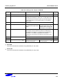
TD0CON — Timer D0 Control Register
FAH
Set 1, Bank 1
Bit Identifier
.7
.6
.5
.4
.3
.2
.1
.0
RESET Value
0
0
0
0
0
0
0
0
R/W
R/W
R/W
R/W
R/W
R/W
R/W
R/W
Read/Write
Addressing Mode
Register addressing mode only
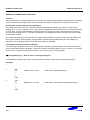
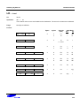
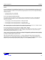
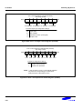
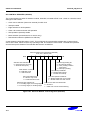
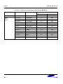
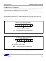
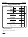
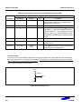
.7–.5
Timer D0 Clock Selection Bits
.4–.3
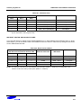
.2
.1
.0
0
0
0
fxx/1024
0
0
1
fxx/256
0
1
0
fxx/64
0
1
1
fxx/8
1
0
0
fxx/1
1
0
1
External clock (TD0CLK) falling edge
1
1
0
External clock (TD0CLK) rising edge
1
1
1
Counter stop
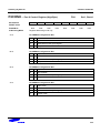
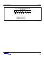
Timer D0 Operating Mode Selection Bits
0
0
Interval mode (TD0OUT)
0
1
Capture mode (Capture on rising edge, counter running, OVF can occur)
1
0
Capture mode (Capture on falling edge, counter running, OVF can occur)
1
1
PWM mode (OVF and match interrupt can occur)
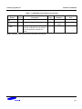
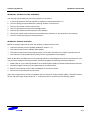
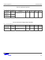
Timer D0 Counter Clear Bit
0
No effect
1
Clear the timer D0 counter (when write)
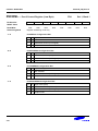
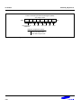
Timer D0 Match/Capture Interrupt Enable Bit
0
Disable interrupt
1
Enable interrupt
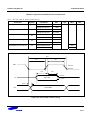
Timer D0 Overflow Interrupt Enable Bit
0
Disable overflow interrupt
1
Enable overflow interrupt
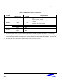
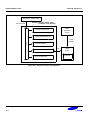
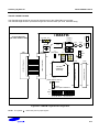
NOTE: The TD0CON.2 value is automatically cleared to "0" after being cleared counter.
4-68