1
Using Your
M68DKIT912C32
Microcontroller Kit
www.technologicalarts.com
DISCLAIMER
While we have made every effort to avoid errors in the preparation of this manual, we
cannot be held responsible for any misinformation or omissions that may have occurred.
Furthermore, as manufacturer of this product, Technological Arts’ sole liability and the buyer’s exclusive remedy shall be refund of the amount paid or repair or replacement of the
product, at the manufacturer’s option. The manufacturer disclaims all other warranties, expressed or implied, including but not limited to implied warranties of merchantability and
fitness for a particular purpose, with respect to the product and accompanying written material, hardware, and firmware. In no event shall the manufacturer or its suppliers be held
liable for any damages whatsoever (including, without limitation, damages for loss of business profits, business interruption, loss of business information, or any other loss) arising out
of the use of, or inability to use, the product, even if the manufacturer has been advised of
the possibility of such damages. The product is not designed, intended, nor authorized for use
in applications in which the failure of the product could bring about a scenario in which personal injury or death may occur. If used in any such unintended or unauthorized application,
the manufacturer and its suppliers shall be held harmless against all claims, even if any such
claim alleges that the manufacturer was negligent regarding the design or implementation of
the product.
Product features, availablility, and prices may change without notice.
All trademarks used in this document are the property of their respective holders.
PRECAUTIONS
1) Electro-Static Discharge (ESD) prevention measures should be followed when handling
this product. ESD damage is not covered by the warranty.
2) Electro-magnetic Compatibility:
a) This product, as shipped from the factory with associated power supply and cables,
has been tested to meet the requirements of CE and the FCC as a “Class A” product.
b) This product is designed and intended for use as a platform for the development of
hardware or software in an educational or professional laboratory.
c) In a domestic environment this product may cause radio interference in which case
the user may be required to take adequate prevention measures.
d) Attaching additional wiring to this product or modifying the product’s configuration
from the factory default may affect its performance. Such alteration may cause
interference with other apparatus in the immediate vicinity. If such interference is
detected, suitable preventive measures should be taken.
1 Introduction
1.1
Congratulations!
With M68DKIT912C32, you are now ready to explore the power and versatility of the
latest member of Motorola’s most advanced 16-bit microcontroller family! Whether you’re
new to Motorola microcontrollers or you’ve used some of the earlier ones, such as 68HC05,
68HC11, or 68HC12, you’ll be impressed with the well thought-out design and implementation of the 9S12C family. And the ‘DKIT912C32 gives you the opportunity to explore the
9S12C family’s potential at a very affordable price! Add to that the proven advantages of it’s
popular design approach, and you’ll see why you picked a real winner!
1.2
Support
To help you get the most out of this product, and to make the experience as enjoyable
and productive as possible, we’ve put together a comprehensive website, loaded with resources, support, and applications information. If you experience any difficulties, or need
help with your application, the World Wide Web is arguably the most valuable resource available to you. There you’ll find the latest information, software, and troubleshooting help, as
well as discussion groups where you can network with people around the globe to get the
answers you need. So if you still need help, or have questions after reading this manual and
perusing the contents of the included CD, visit our website: www.technologicalarts.com and
tap into the collective! Pay particular attention to our Support, Applications, and Resources
webpages. While on our Support page, be sure to join our techart-micros discussion group
and Motorola’s HC12 discussion group.
1.3
Product Configuration
M68DKIT912C32 was designed as a versatile evaluation and application tool for the
Motorola MCS12 “C” family of microcontrollers. While it is based on the 9S12C32, it is also
suitable for developing applications for any of the forthcoming derivatives (9S12C64,
9S12C96, 9S12C128, etc.). All of the subsystems are identical, with the differentiating factor
among the chips being the amounts of Flash and RAM offered.
In addition to the MCU module (M68MOD912C32), the M68DKIT912C32 includes a
Docking Module, which provides convenient support circuitry for working with the microcontroller. This includes a power regulator, a socket for the MCU module, a couple of user LEDs
and pushbuttons, and a snap-off prototyping area. A power supply and serial cable are included with the kit to help you get plugged in. A resource CD containing this manual, example programs, and all the MCU documentation, along with a CodeWarrior C compiler on CD
complete the package.
The M68MOD912C32 MCU module is supplied in a 32-pin DIP footprint that plugs into
the 40-pin DIP socket on the Docking Module. The Docking Module is designed to support
other MCU modules to be introduced later in 24-pin and 40-pin DIP packages.
A BDM connector is provided on the MCU Module for development tool application and
is compatible with standard HCS12 BDM interface cables and software.
1.4
Features and Specifications
The design consists of two parts: a ‘C32 MCU Module in 32-pin wide DIP form-factor, and
a Docking module which provides a programming interface with a personal computer. The
MCU module, once programmed, can be used independent of the Docking Module, and is
compatible with standard 0.6” wide DIP sockets and solderless breadboards.
1
Rev. 1
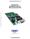
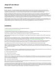
Figure 1 - Identification of Hardware Features
9S12C32 MCU Module
Voltage Regulator
RS232C Interface
BDM Connector
8 MHz Crystal
6-pin BDM Connector
M68DEMO9S12C32
MOTOROLA
9S12C32 MCU
0.6”
Boot/Run Switch
TOP VIEW
END VIEW
BOTTOM VIEW
PINOUT
9S12C Docking Module
DC Voltage In
(use J1 or J2)
Adjustable
Regulator
Select 3.3V or
‘Scope Grounding Point
5V operation
Power LED
Snappable
Prototyping
Area
Reset Button
9-pin RS232
Connector
CAN options
(for 40-pin DIP
version only)
CAN connector
(for 40-pin DIP
version only)
User LEDs
User Buttons
CAN termination
(for 40-pin DIP
version only)
2
Socket accomodates
24-, 32, and 40-pin
MCU Modules
Optional Expansion
Connectors
The MCU module includes the following features:
• 9S12C32 MCU in 48-pin LQFP
• 8 Mhz crystal
• PLL circuit
• local 5 Volt low-dropout 100 mA regulator
• RS232 transceiver circuit
• standard 6-pin BDM connector
• on-chip Serial Monitor
• BOOT/RUN switch to support Serial Monitor
• 32K Bytes Flash
• 2K Bytes Ram
• user access to 16 digital port lines, including Port M, Port T, and PORTE
• user access to eight 10-bit analog input or digital I/O port lines (Port AD)
• five PWM timer channels (PT0 - PT4)
• eight Input Capture/Output Compare (Port T)
• serial peripheral interface (SPI)
• serial communications interface (SCI)
• controller area network (CAN 2.0)
• key wake-up inputs
• user access to MCU reset signal
• background debug mode (BDM) connector
• pinout is super-set of competing 24-pin modules on the market
The Docking Module implements the following features:
• 9-pin D-sub socket for serial interface to user personal computer
• dual-voltage regulator configuration to permit user-selectable 3.3V and 5V
operation
• low-dropout, low-power regulator, with thermal shutdown and reverse-polarity
protection
• polarized power connector to prevent reverse polarity application by user
• oscilloscope grounding point
• high-efficiency green LED power indicator
• reset button
• 40-pin DIP socket to accomodate a range of modules from 24 to 40 pins
• rubber feet
• user application support features:
- dual high-efficiency red user LEDs (PT0, PT1)
- dual user pushbuttons (PAD0, PAD1)
- snappable prototyping area (sea of plated-through holes on 0.1” grid)
- accomodation for dual 40-pin I/O bus expansion connectors (user-installed
option)
- expansion connectors supports available accessories (eg. standard ribbon
cable, prototyping card, motor driver, etc.)
Specifications:
• MCU Module:
size: 1.7” x 0.75”
pin-spacing: 0.1” x 0.6”
pin 1 location: 0.75” x 0.05” (with respect to corner of circuit board)
pins: 0.03” round, machined, gold-plated
input voltage range (Vin): 5 to 15VDC
current draw: 25 mA, nominal (@24 MHz bus speed)
• Docking Module:
Power Input: +6 to +20VDC, 9VDC typical
Current Draw: 5 mA, nominal, with 9VDC input
Documentation:
• Quick Start Guide (2-page hardcopy)
• schematics and pinout/component placement drawings (on CD)
• manual with details of design features, suggested uses, and examples (on CD)
• datasheets on all semiconductors used in the design
3
Software:
• Code Warrior CD from Metrowerks
• Resource CD (Serial Monitor GUI for Windows, code examples, schematic, manual,
data sheets, etc.)
1.5
M68DKIT912C32 vs. Traditional Evaluation Boards
Most available evaluation and development systems tend to be too expensive and
bulky for embedding into a real application, so they lie on a shelf gathering dust once you’ve
reached a certain point in the learning curve. Or maybe you think up some clever way to
hack it apart and make it fit inside your robot or product prototype. Even then, the prototyping area provided is often limited, and does not lend itself to re-usability. And what if you
burn out a chip the night before the contest or product demo? What a mess to repair or redesign!
The M68DKIT912C32 solves all of these problems and more! Since the MCU module is
packaged in a standard 32-pin DIP footprint, it is modular and re-usable. It can simply be
plugged into your application, or moved from one application board to another, allowing your
whole system to be re-configured at the last minute. The prototyping area on the Docking
Module offers you a platform for your initial application, which can be snapped off and discarded when you no longer need it. Two 40-pin connector footprints remain, and can be used
with various types of connectors, ribbon cables, backplanes, prototyping cards, etc. that are
available now or are under development. Make a point to visit our website from time to time,
just to see what’s new.
The detachable nature of the prototyping card means that you can easily replace it
with other cards, including some application cards available from Technological Arts. You can
build up a collection of different application circuits, and use them all with the same microcontroller board. Of course, if the prototyping card approach doesn’t suit you, the standard
32-pin DIP format of the MCU Module makes it easy for you to incorporate it into your own
designs. In fact, it’s pinout is a superset of the popular 24-pin DIP MCU modules available
from other vendors. You can plug it into a DIP socket in your application, or directly into a
solderless breadboard.
The modular nature of this product is especially advantageous in an educational environment, where the student can progress from simple to more complex applications throughout a semester, or from one course to the next-- even incorporating the board into a final
project. In fact, where budgets are tight, different students can share the same microcontroller module, and plug in their own interface cards when it’s their turn to use it.
1.6
Resident Debug/Monitor
Residing in a 2K protected block of on-chip flash memory is Motorola’s versatile Serial
Monitor program. When used with the included (on CD) free uBug12 Windows application
running on a personal computer, you can display and edit memory and registers, erase and
program flash, set breakpoints, and do instruction tracing. In Run Mode, your program runs
automatically from Flash, following reset. See Chapter 2 and Appendix A for details on
uBug12 and the resident monitor.
1.7
Communications
An RS-232C serial interface port (RX & TX only) is included on the Docking Module,
allowing communication with a PC com port, or any other device which has an RS-232 serial
port. The RS-232 channel (implemented via the SCI of the MCU) is available via a 9-pin
D-sub connector on the Docking Module. When the MCU Module is reset in Load mode, the
resident serial monitor uses this port to communicate with an appropriate program running
on your PC.. In RUN mode, the port is available for your application.
While the MCU does supports Controller Area Network (CAN), no physical layer circuit
is provided. If you would like to use CAN, you’ll need to add the appropriate transceiver cir4
cuit externally to PM0 and PM1 (pins 18 and 17 of the MCU module).
In passing, it should be mentioned that the MCU also supports SPI. Since this is a
logic-level protocols, meant for local communications among peripheral chips, no transceivers
are required nor are they provided. Commonly used SPI chips and modules include serial
memory, temperature controllers, clock/calendar chips, DACs, MP3 decoders, etc. See the
MCU datasheets for details on these subsystems.
5
2 Getting Started
2.1 Introduction
Support software for the M68DKIT912C32 is designed to be used with any computing
platform running one of the Windows 98/NT/2000/XP operating systems. Users should also
familiarize themselves with the hardware and software operation of the target HCS12 device.
Refer to the Motorola 9S12C Family Device User Guide and the CPU12 Reference Manual for
details. The ‘DKIT912C32 serves to promote the features of the 9S12C32 device and to assist
the user in quickly developing an application within a known working environment. Users
who are familiar with memory mapping techniques, various memory types, and embedded
software design are likely to experience the most successful and rapid application development.
Development may be performed through the resident Serial Debug Monitor, or by attaching a compatible HCS12 BDM cable and employing supporting host software. The Serial Monitor utilizes the SCI port as its connection to the host PC, and does not use the traditional
background debug mode, thus eliminating the need for a BDM pod or cable.
The Serial Monitor interfaces with a program running on a host personal computer (PC) to
provide an effective, low-cost debug approach. The Serial Monitor provides the user with the
ability to erase and program the MCU’s Flash memory, and also to load and debug application
programs. Windows-based host software (uBug12) is included to provide an interface to the
monitor. Host support is also built into the CodeWarrior C Development environment .
Serial Monitor firmware resides in a 2K protected block of the MCU’s internal flash memory, and reserves some of the MCU resources for its operation. Refer to Appendix A and
Motorola’s Serial Monitor application note for details.
Once a user program has been loaded into Flash via monitor contorl, the BOOT/RUN
switch (SW1) on the MCU Module determines whether control is passed to the user program
(RUN) or to the Serial Monitor. The Monitor will remain in protected flash memory for future
use if needed. It is possible to erase and re-load the Serial Monitor via a BDM pod.
2.2 Getting Started with uBug12
• Perform a quick visual check of the MCU Module and Docking Module for any damage during transit
• Ensure that the MCU Module is properly oriented and seated in the Docking Module’s 40-pin socket
(square white dot indicates pin 1)
• Connect the Docking Module’s RS232 port (J3) to a COM port of a personal computer, using the cable supplied
• Locate and install the Windows application called uBug12, included on the CD (also on webpage). You will also
need to install the Microsoft .NET framework (included on CD) if it is not already on your computer.
• Launch uBug12
• Activate the serial port connection by entering CON x (where x is the COM port you are using; usually 1 or 2)
• Set switch SW2 to the BOOT position
• Connect the supplied power source to barrel jack J2
• uBug12 will display a short message, followed by its command prompt
• The Monitor is now ready for your commands (see Appendix B for full list of uBug12 commands)
2.3 Loading a Program via uBug12
To download one of the supplied example programs into flash and execute it, follow these steps:
• Type fbulk <enter> at the uBug12 prompt to erase any existing program
• Type fload ;b <enter>
• From the displayed file browser, select one of the example program’s output files (they will have a filename
extension of .s19, .s2 or .sx)
• After loading has finished, move SW2 to the RUN postion, and press the Reset button (SW1)
• If you wish to debug the program, move SW2 back to the BOOT position and press Reset
• The uBug12 prompt will appear
• Use Monitor commands to debug your code, if desired
6
2.4 Getting Started with CodeWarrior 3.0
1) Attach included serial cable between Docking Module serial port and an available COM port on the host PC.
2) Install uBug12 Serial Monitor user interface software on the host PC
3) Ensure that the MCU Module is properly oriented and seated in the Docking Module 40-pin socket (square
white dot indicates pin 1)
4) Plug in the included power supply, and attach it to J2 of the Docking Module
5) Verify that Power LED D1 is illuminated.
6) Move MCU Module BOOT/RUN switch SW1 to BOOT position
7) Press Docking Module RESET button SW1 to enable the Serial Monitor.
8) Install CodeWarrior and launch it
9) Create a new project:
Click File
Click New
Click HC(S)12 Project Wizard
In the dialog box for Project Name, type Example1, select OK
Click on MC9S12C32, select Next
Click C Programming, select Next
Click No to Processor Expert, select Next
Click No to PC Lint, select Next
Click None for Floating Point, select Next
Click Small for Memory Model, select Next
Click Motorola Serial Monitor Hardware Debugging, select Next
10) Copy and paste the follwing code into the main.c file. (under Sources in the project window)
------------------------------------CODE------------------------------------------------#pragma CODE_SEG DEFAULT
void main(void) {
DDRT = 0x03;
ATDCTL23 = 0x0;
ATDCTL45 = 0x0;
ATDDIEN = 0xFF;
while(1){
PTT = ~(PTAD/64);
}
}
--------------------------------CODE------------------------------------------------------------
7
11) Click on Project -> Make (F7)
12) Launch uBug12
13) Type con 1 or con 2 (to connect to the comport you are using)
14) Type fbulk to ensure flash is erased
15) Type fload ;b
16) Navigate to "My Documents\Example1\Bin\ " and select the .s19 file (it should have the name
Monitor.abs.s19)
17) Type go
18) Now when you press either of the user buttons on the Docking Module, the corresponding user
LED will glow.
2.5 Serial Monitor Operation
Refer to the Serial Monitor application note (AN2548) for complete details of operation.
The following paragraphs present the basics. The Monitor resides in a 2K byte protected
block of Flash memory, and uses about 50 bytes of stack space. It implements a binary command set via the HC12 SCI port. Serial communication is enabled at 115.2Kbps, using the
MCU’s SCI Interrupt features. The Monitor enables the PLL to boost the MCU bus speed to
24Mhz.
2.6 Commands
Unlike previous HC12 resident debuggers (eg. D-Bug12), the Serial Monitor does not
implement a text-based (ASCII) command set. Instead, the command set is binary, which
means a user interface is required on the host pc. This approach allows the Monitor to occupy
a very small footprint, yet retain a high level of functionality. As a result, however, it is not
possible to enter commands directly via a terminal program (eg. HyperTerminal).
2.7 Interrupt Service Support
The Monitor implements vector relocation in the 9S12C32 Flash (also known as pseudovectors). The user interrupt vectors are implemented in a block of non-protected Flash from
0xF780 to 0xF7FF. SCI, SWI, and RESET vectors are inaccessible to the user while the monitor is operating. Programming the user Reset vector will cause the monitor to execute the
user program upon Reset.
2.8 Monitor Memory Map
0x0000 - 0x03FF
0x0400 - 0x37FF
0x3800 - 0x3FFF
0x4000 - 0x7FFF
0x8000 - 0xBFFF
0xC000 - 0xF77F
0xF780 - 0xF7FF
0xF800 - 0xFFFF
9S12C32 Register Space. See the 9S12C32 User Manual for details
Not used
9S12C32 Ram space, user application ram Initial Monitor stack = 0x3FFF (reserve 50
bytes)
User Application Flash Memory
Do not use
User Application Flash Memory
User Interrupt Vectors
Monitor Flash Memory Space (Protected)
8
3 M68DKIT912C32 Operation
The M68DKIT912C32 provides input and output features to assist in application development. These features may be isolated from the applied HCS12 I/O ports by the option jumpers. This allows alternate use of the HCS12 I/O ports for other application and connection on
the I/O port connectors. Caution should be observed so that the HCS12 I/O port pin applied
to an on board feature is not also applied to external components by the user.
3.1 Power Supply
Input power is applied by external connection to the J1 or J2 power jack of the Docking
Module. J1 is an optional power input, compatible with a 2-pin Molex connector (pin 1 is
positive). J2 is the the default external power input to the board. It accepts a standard
2.1mm center barrel plug connector (center positive) to provide the VIN supply of +6 to
+20VDC (+9VDC typical). A 9VDC power supply is included with M68DKIT912C32 for this
purpose. VIN is fed to voltage regulator U2, which provides the regulated +5V supply (VDD)
for the MCU Module. By placing a shunt on JB1, 3.3V operation is enabled.
3.2 MCU Module Power
If the MCU Module is to be operated independent of the Docking Module, a supply of +6 to
+15VDC can be applied across VIN (pin 32) and VSS (pin 31). The onboard regulator is capable of supplying a total of 100 mA. Since the MCU Module uses about 25 mA, an additional 75
mA or less of regulated 5V is available for user applications via the VCC pin (29). If a BDM
pod is connected to the BDM connector (J1), it will probably require all or most of the available 5V power. If a BDM pod with external power supply is used, this is not an issue. Check
the specifications of the BDM pod to be used to ensure compatibility. If the current draw is
too large, the on-board regulator will enter thermal shutdown, and the module will stop working until the overcurrent condition is resolved.
Optionally, a regulated 5V or 3.3V supply may be fed directly into the VCC pin (pin 29) of
the MCU Module. In this configuration, VIN should be left open, and the on-board regulator is
unused.
3.3 Reset Switch
Reset Switch operation will place the MCU in the Reset state. Caution: the RESET switch
should not be pressed while a BDM cable is connected to the MCU Module. Instead, the BDM
should control Reset generation via the connection on the BDM connector.
3.4 MODA and MODB Options
The 48-pin version of 9S12C32 used on the MCU Module supports Single-chip mode by
default. MODA, MODB, and address/databus signals are not pinned out, so it is not possible
to operate the MCU in expanded modes.
3.5 MODC Option
MODC selects Special Background Mode when in the GND or logic low state. MODC is in
the default Normal mode position at all times unless a BDM cable is attached to the BDM
connector.
3.6 J3 RS232 Port
Connector J3 on the Docking Module provides the connection point for a standard RS232C compatible serial port controlled by the MCU’s SCI port. The physical interface transceiver circuit is implemented on the MCU Module itself, and the signals TX (pin1) and RX
9
(pin2) of the MCU Module socket are routed to the 9-pin D-sub connector J3 on the Docking
Module. PB4 of the MCU is used for an optional DTR signal, which may be implemented by
the user. Note that the Monitor communication does not implement the DTR signal.
3.7 BDM Connector
For proper functioning of a BDM pod, pin 1 on the BDM cable must mate with pin 1 of the
BDM connector on the MCU Module. The location of pin 1 is marked with a square white dot.
The cable usually has a colored stripe on one edge, and/or an index mark on the connector.
If the BDM pod you are using has a 10-pin plug, only the first six pins are used-- let the
other four pins overhang the connector, as shown in the photo below.
10
4 Software Considerations
4.1 Using the Serial Monitor
When you are working without a BDM pod, the Serial Monitor program is the only method
available to load and erase flash. It is in a protected block of flash, so there’s virtually no way
to accidentally erase it. There are two modes, controlled by switch SW2: Run and Load. The
monitor mode is determined immediately following reset by checking the position of switch
SW2. When working with the monitor program in place, there are a few points to be noted:
1) while the user vectors are implemented by the monitor at 0xF780 to 0xF7FF, you don’t
really have to worry about it, because the monitor program will automatically adjust them
when your s-record is loaded. It’s good to know, however, so you don’t get alarmed
when you are snooping around in the vector area and don’t see what you expected.
2) the monitor relocates RAM to the address range 0x3800 to 0x4000 from the default
location after MCU reset of 0x0000 to 0x07FF.
3) the monitor program enables the phase-locked loop (PLL), so the target is running at
a bus speed of 24MHz (when in LOAD mode) and not at the startup bus speed of 4Mhz.
If you intend to use the PLL, you’ll need to enable it in your code, though.
4) the user code must clear the CCR I-Bit (eg. via CLI instruction in assembler).
5) SCI0 cannot be used by the user program when in BOOT mode, since it is dedicated to
the monitor program; however, it is available to the user in RUN mode.
6) COP cannot be disabled in BOOT mode.
4.2 Using a BDM Pod
You can ignore the on-chip serial monitor altogether if you have an appropriate BDM pod
(such as the MicorBDM12SX, from Technological Arts). When using a BDM pod, you’ll find
that the memory resources are mapped as per the Motorola documents, following a reset
event. So your program will need to take care of any desired initializations to relocate resources or enable PLL, as relevant to your application.
If you use an assembler or compiler other than CodeWarrior, you’ll probably need to use
the SRecCvt utility to properly format the s-records generated by the compiler/assembler
before attempting to load them into the target chip’s flash. Use the following command line:
sreccvt.exe -m C0000 FFFFF 32 -lp -o outfile.s2 infile.s19
where infile refers to the file you are converting and outfile is the result
11
5 Tutorial
As mentioned in the Quick Start Guide included with the M68DKIT912C32, the MCU Module is shipped from the factory with a Demo program loaded into its memory. This program is
useful for familiarizing yourself with the hardware features of the MCU. It was written in
assembler, using Motorola’s MCUez Windows integrated development environment
(http://e-www.motorola.com/files/soft_dev_tools/software_tools/ide_integrated_
development_environment_/MCUEZIDE.html). The sourcecode can be found on the included Resource CD, if you would like to examine or modify it.
If you’ve already erased the demo program, you may use uBug12 to re-load it. Then
follow the relevant steps in the QuickStart Guide to open HyperTerminal and achieve the
display shown below.
5.1 Executing Demo Commands
• Type the digit 0 repeatedly and observe that LED D2 toggles on and off.
• Type the digit 1 repeatedly and observe that LED D3 toggles on and off.
• Type the letter F to cause LED D2 to flash twice.
Typing E, H, M, or T will cause a hex number to be displayed, whose bit values represent
V CC
the logic levels of the respective pins. If
the pins are unconnected to external circuitry, they will assume a logic 1 level,
due to internal pullup resistors.
1
LS1
D1
1N4148
5.2 A Simple Audio Circuit
Connect a simple audio transducer
circuit, as shown, and type the letter F.
LED D2 will flash twice, and two audible
“beep” tones will be emitted from the
transducer. If you press and release the
PT0
PIN 27 on H1 HEA DER
12
1
R1
4K7
2
2
2
Q1
2N3904
V CC
Reset button on the Docking module, LED D2 will flash
four times, and you’ll hear four “beep” sounds from the
transducer.
R1
LIGHT SENSOR
5.3 A Simple Analog Circuit
Connect a CdS light sensitive resistor (photocell) in
the configuration shown. Then type the letter R to see
the value of AN00 change as you vary the amount of light
reaching the photocell. The value displayed is a 10-bit
representation of the voltage level on the AN00 pin, with
fullscale being approximately 5V (represented by the
hexadecimal number 3FF).
13
A N00
PIN 5 on H1 HEA DER
R1
10K
14
Appendix A - Serial Monitor
Introduction
This appendix describes the Motorola 2 Kbyte monitor program for the HC9S12 series
MCU. This program supports 23 primitive debug commands to allow FLASH / EEPROM programming and debug through an RS232 serial interface to a personal computer. These include commands to reset the target MCU, read or modify memory (including FLASH /EEPROM
memory), read or modify CPU registers, go, halt, or trace single instructions. In order to allow
a user to specify the address of each interrupt service routine, this monitor redirects interrupt
vectors to an unprotected portion of FLASH just below the protected monitor program. This
monitor is intended to be device unspecific, this single application with very slight modification should execute on any HC9S12 derivative. A user on a tight budget can evaluate the MCU
by writing programs, programming them into the MCU, then debug using only a serial I/O
cable and free software (uBug12) for their personal computer.
This monitor does not use any RAM other than the stack itself. The COP watchdog is utilized for a cold reset function; user code should not disable the COP (ie. by writing 0x00 to
COPCTL). This development environment assumes you reset to the monitor when you are
going to perform debug operations. If your code takes control directly from reset, and then
an SCI0 interrupt or a SWI attempts to enter the monitor, the monitor may not function because SCI0, the phase locked loop (PLL), and memory initialization registers may not be
initialized as they would be for a cold reset into the monitor. There is no error handling for the
PLL. If the frequency source is missing or broken, the monitor will not function. The monitor
sets the operating speed of the MCU to 24 MHz. Modification of the MCU speed by the user
with out considerations for the monitor program will render the monitor nonfunctional. If the
PLL loses lock during operation, the monitor will fail.
Block Protection
In order to prevent accidental changes to the monitor program itself, the 2 Kbyte block of
FLASH memory where it resides ($F800-$FFFF), is block protected. Additionally all write commands are restricted from modifying the monitor memory space. The only way to change the
contents of this protected block is to use a BDM-based development. In the lowest cost applications where the monitor is used with an SCI serial interface to the RS232 serial port on a
personal computer, there is no way to accidentally erase or modify the monitor software.
COP Configuration
The monitor as written creates hard reset function by using the COP watchdog timer. It
does so by enabling the COP and waiting for a COP timeout reset to occur. If the user application uses the COP two issues must be considered.
• If the COP is disabled in the user application, the monitor will be unable to perform a
hard reset and will soft reset to the start of the monitor instead.
• The monitor does not service the COP timer. If the user application implements COP
timer servicing, upon re-entry into the monitor a hard reset is likely to occur.
Memory Configuration
1) Register space is $0000-$03FF.
2) Flash memory is any address greater than $4000. All paged addresses are assumed to
be Flash memory.
3) RAM ends at $3FFF and builds down to the limit of the device’s available RAM.
4) External devices attached to the multiplexed external bus interface are not supported.
15
Serial Port Usage
In order for this monitor to function the SCI0 serial interface is used. It is assumed that
the monitor has exclusive use of this interface. User application code should not implement
communications on this serial channel. This monitor accommodates RS232 serial communications through SCI0 at 115.2 kbaud. For applications requiring the use of SCI0, you should
purchase a BDM pod which allows for more advanced debugging.
Vector Redirection and Interrupt Use
Access to the user vectors is accomplished via a jump table located within the monitor
memory space. This table points all interrupt sources to a duplicate vector table located just
below the monitor. ($F780-$F7FE). The monitor will automatically redirect vector programming operations to these user vectors. The user’s code should therefore continue to implement the normal (non-monitor) vector locations ($FF80-$FFFE). If execution of an interrupt
with an un-programmed vector is attempted, behavior is undefined. For this reason, the user
is strongly encouraged to implement a software trace for all vectors, as is good programming
practice. The monitor depends on interrupts being available for monitor re-entry after GO or
TRACE commands. Therefore, it is important that the user application executes with interrupts enabled.
16
APPENDIX B - uBUG12 Command LIST
-------------------------------------- REGISTERS ----------------------------------------RD
- Register Display
RM
<RegisterName> <Data8/16>
- Register Modify
CCR
<Data8>
- Set CCR register
D <Data16>
- Set D register
PC <Data16>
- Set PC register
PP <Data8>
- Set PP register
SP <Data16>
- Set SP register
X <Data16>
- Set X register
Y <Data16>
- Set Y register
----------------------------------- MEMORY MODIFY -----------------------------------BF <StartAdd> <EndAdd> <Data8>
- Block fill
BFW
<StartAdd> <EndAdd> <Data16> - Block fill word
MD <StartAdd> [<EndAdd>]
- Memory display
MDW
<StartAdd> [<EndAdd>]
- Memory display word
MM <Address> <Data8>
- Memory modify byte
MMW
<Address> <Data16>
- Memory modify word
------------------------------------------- FLASH -------------------------------------------FBULK
- Flash bulk erase
FLOAD
[;B][;M]
- Flash load
--------------------------------------- DEVICE INFO -------------------------------------DEVICE
- Get device name
---------------------------------------- GO/HALT -------------------------------------------GO [<StartAddress>]
- Start execution
HALT
- Halt execution
RESET
- Reset target
------------------------------------------- GUI ------------------------------------------------CON
<Comport>
- Connect to target
DISCON
- Disconnect from target
EXIT
- Terminate GUI
HELP
- Display help
OP <Opacity%>
- Set main GUI opacity
17
APPENDIX C - M68MOD912C32 Pinout
18