1
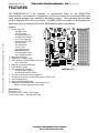
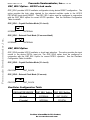
Freescale Semiconductor, Inc.
M68EVB912C32
Freescale Semiconductor, Inc...
Evaluation Board for Motorola MC9S12C32
! Axiom Manufacturing • 2813 Industrial Lane • Garland, TX 75041
Email: [email protected] Web: http://www.axman.com !
For More Information On This Product,
Go to: www.freescale.com
M 6 8 E V B 9 1 2 C 3 2
Freescale Semiconductor, Inc. 0 5 / 1 5 / 0 3
CONTENTS
CAUTIONARY NOTES ...........................................................................................................................................................3
TERMINOLOGY ......................................................................................................................................................................3
FEATURES................................................................................................................................................................................4
GETTING STARTED...............................................................................................................................................................5
M68EVB912C32 STARTUP ..................................................................................................................................................5
REFERENCE DOCUMENTATION .................................................................................................................................................6
DEBUG MONITOR OPERATION .........................................................................................................................................6
MONITOR MEMORY MAP: .................................................................................................................................................7
Freescale Semiconductor, Inc...
M68EVB912C32 BOARD OPERATION................................................................................................................................7
POWER SUPPLY ...................................................................................................................................................................7
ON_OFF Switch ..................................................................................................................................................................7
PWR - Power Jack ...............................................................................................................................................................8
TB1 - Power Access Term Block..........................................................................................................................................8
VDDR_EN ...........................................................................................................................................................................8
RESET AND RESET CONFIGURATION .....................................................................................................................................8
RESET SWITCH ..................................................................................................................................................................9
LV1 Reset Generator ...........................................................................................................................................................9
LV1_EN Option ...................................................................................................................................................................9
RESET Indicator..................................................................................................................................................................9
MODA and MODB Options.................................................................................................................................................9
MODC Option ...................................................................................................................................................................10
ROM_EN Option ...............................................................................................................................................................10
TEST Option ......................................................................................................................................................................10
OSCILLATOR X1 AND Y1........................................................................................................................................................10
OSC_SEL1 Option – HCS12 clock mode ..........................................................................................................................11
OSC_SEL2 Option .............................................................................................................................................................11
Oscillator Configuration Table .........................................................................................................................................11
COM1 (SCI) PORT .................................................................................................................................................................12
COM1 Connection .............................................................................................................................................................12
RX_EN Option ...................................................................................................................................................................12
RTS_EN and CTS_EN Options..........................................................................................................................................12
CAN PORT .............................................................................................................................................................................13
CAN_TXEN and CAN_RXEN Options ..............................................................................................................................13
RS Test Pad and Cut Option 1...........................................................................................................................................13
RC11,12,and 13 CAN Terminations ..................................................................................................................................14
LED 1-8 INDICATORS AND LED_EN OPTION ........................................................................................................................14
SW1 DIP SWITCH AND SW1_EN OPTION .............................................................................................................................14
OPTIONAL SERIAL EEPROM .................................................................................................................................................14
M68EVB912C32 I/O PORT CONNECTORS ......................................................................................................................15
ANALOG AND PAD0-7 I/O PORT CONNECTOR ....................................................................................................................15
VRH_EN and VRL_EN Options.........................................................................................................................................15
MCU I/O PORT CONNECTOR..................................................................................................................................................16
BDM PORT...........................................................................................................................................................................16
2 On This Product,
For More Information
Go to: www.freescale.com
M 6 8 E V B 9 1 2 C 3 2
Freescale Semiconductor, Inc. 0 5 / 1 5 / 0 3
Cautionary Notes
1) Electrostatic Discharge (ESD) prevention measures should be applied whenever handling
this product. ESD damage is not a warranty repair item.
2) Axiom Manufacturing does not assume any liability arising out of the application or use of
any product or circuit described herein; neither does it convey any license under patent
rights or the rights of others.
3) EMC Information on the M68EVB912C32 board:
Freescale Semiconductor, Inc...
a) This product as shipped from the factory with associated power supplies and cables, has
been tested to meet with requirements of CE and the FCC as a CLASS A product.
b) This product is designed and intended for use as a development platform for hardware
or software in an educational or professional laboratory.
c) In a domestic environment this product may cause radio interference in which case the
user may be required to take adequate prevention measures.
d) Attaching additional wiring to this product or modifying the products operation from the
factory default as shipped may effect its performance and also cause interference with
other apparatus in the immediate vicinity. If such interference is detected, suitable
mitigating measures should be taken.
Terminology
This development board applies option selection jumpers. Terminology for application of the
option jumpers is as follows:
Jumper on, in, or installed = jumper is a plastic shunt that fits across 2 pins and the
shunt is installed so that the 2 pins are connected with the shunt.
Jumper off, out, or idle = jumper or shunt is installed so that only 1 pin holds the shunt,
no 2 pins are connected, or jumper is removed. It is recommended that the jumpers be
idled by installing on 1 pin so they will not be lost.
This development board applies hardwired option selections for several option jumper
selections. This option selection applies a circuit trace between the option pads to complete a
default connection. This type connection places an equivalent Jumper Installed type option.
The circuit trace between the option pads may be cut with a razor blade or similar type knife to
isolate the default connection provided. Applying the default connection again can be
performed by installing the option post pins and shunt jumper, or by applying a wire between
the option pads.
3 On This Product,
For More Information
Go to: www.freescale.com
M 6 8 E V B 9 1 2 C 3 2
Freescale Semiconductor, Inc. 0 5 / 1 5 / 0 3
FEATURES
Freescale Semiconductor, Inc...
The M68EVB912C32 is an evaluation or development board for the MC9S12C32
microcontroller. Development of applications is quick and easy with the included DB9 serial
cable, sample software tools, examples, and debug monitor. The prototyping area provides
space to apply the MCU I/O to your needs. The BDM_PORT is provided for development tool
application and is compatible with HCS12 BDM interface cables and software.
Features:
♦ MC9S12C32 CPU
* 32K Byte Flash
* 2K Bytes Ram
* 61 I/O lines (80 pins)
* 6 PWM Timer channels
* 8 I/O Timer Channels
* 8 Channel 10 BIT A/D
* SPI Serial Port
* SCI Serial Port
* CAN 2.0 Port
* Key Wake-up Ports
* BDM DEBUG Port
* Clock generator w/ PLL
* Up to 25Mhz operation
♦ 8Mhz Clock Oscillator
♦ Regulated +5V power supply
♦ SCI1 Serial Port w/ RS232 DB9-S Connector
* SCI1 Serial Port
♦ CAN Port w/ 1M baud transceiver
♦ Power ON/OFF switch
♦ User Components Provided
* 8 LED Indicators (PB0-7)
* 8 Position DIP Switch (PA0-7)
♦ MCU Port connector provides all digital I/O
♦ Analog Port connector provides analog inputs or PAD0-7 I/O
♦ Large Prototype Area
♦ Optional SPI Serial EEPROM
♦ Supplied with DB9 Serial Cable, Documentation (CD),
Manual, and Wall plug type power supply.
M68EVB912C32
Specifications:
Board Size 5” x 6”
Power Input: +6 to +20VDC, 9VDC typical
Current Consumption: 40ma @ 9VDC input
4 On This Product,
For More Information
Go to: www.freescale.com
M 6 8 E V B 9 1 2 C 3 2
Freescale Semiconductor, Inc. 0 5 / 1 5 / 0 3
GETTING STARTED
Freescale Semiconductor, Inc...
The M68EVB912C32 single board computer is a fully assembled, fully functional development
board for the Motorola MC9S12C32 microcontroller. Provided with wall plug power supply,
support disk, and serial cable. Support software for this development board is provided for
Windows 95/98/NT/2000/XP operating systems.
Development board users should also be familiar with the hardware and software operation of
the target HCS12 device, refer to the provided Motorola User Manual for the device and the
HCS12 Reference Manual for details. The EVB board purpose is to promote the features of
the 9S12C32 device or to assist the user in quickly developing an application with a known
working environment. Users should be familiar with memory mapping, memory types, and
embedded software design for the quickest successful application development.
Application development may be performed by applying the provided embedded serial
interface Debug Monitor, or by applying a compatible HCS12 BDM cable with supporting host
software. The debug monitor dedicates the SCI serial port as its connection to the host PC and
does not use the traditional background debug mode, thus eliminating the necessity for a
background debug mode cable.
The Debug Monitor in conjunction with a program running on a host personal computer (PC)
provides an effective and low cost debug method. Debug monitor operation enables a user to
erase device FLASH memory, program FLASH memory, load application programs, and
debug the application programs. Free host software is available for execution on a PC as an
interface to the monitor.
Debug monitor firmware is provided in the development board HC12 device internal flash
memory and applies some HC12 resources for operation. See the Monitor commands
application note from Motorola for details and the Debug Monitor chapter in this manual for
more information. User applications operated under monitor control may be configured for
dedicated operation by applying the User Reset Vector (0xF7FE/F) and programming the
application into the device flash. The monitor will remain in protected flash memory for future
use if needed.
M68EVB912C32 STARTUP
1) Apply power to the EVB board with the provided wall-plug power supply.
2) Install the provided serial cable between the EVB board COM1 port and an available COM
port on the host PC.
3) Install monitor hosting software on the host PC and launch.
4) Set the EVB board ON - OFF switch to the ON position and verify the POWER indicator is
ON. The EVB is ready to use.
5) Note that if the User Reset vector is programmed, the SW1_EN option jumper must be
installed and SW1 position 6 set to the ON position to enable the monitor.
5 On This Product,
For More Information
Go to: www.freescale.com
M 6 8 E V B 9 1 2 C 3 2
Freescale Semiconductor, Inc. 0 5 / 1 5 / 0 3
Reference Documentation
Reference documents are provided on the support CD in Acrobat Reader format.
Monitor Commands – HCS12 Serial Monitor application note.
9S12C32 manual – 9S12C32 user manuals
CPU12RM – HCS12 core user manual with instruction set
M68EVB912C32_SCH_C.pdf – M68EVB912C32 board schematics
Freescale Semiconductor, Inc...
DEBUG MONITOR OPERATION
See the Monitor commands application note on the monitor for complete details of operation.
Basic operation is provided in this manual. The monitor occupies 2K bytes of flash memory
and about to 50 bytes of stack space. It provides a binary command set via the HC12 SCI port
and COM1 connection. Monitor operation provides a 24Mhz bus or E clock frequency by
default with an 8Mhz reference frequency input.
COMMUNICATION:
The monitor provides 115.2K baud serial communication on the SCI1 interface port. Monitor
applies the SCI Interrupt service in the HC12 device.
POWER ON or RESET PROMPT:
The monitor will provide a binary prompt to the EVB board serial COM1 port.
COMMANDS:
No user commands can be applied with a keyboard with software such as HyperTerminal or
AxIDE. The monitor commands are binary and not compatible with keyboard (ASCII) entry or
display. Host based software should interface with the monitor on the serial communication
port to provide development support.
INTERRUPT SERVICE SUPPORT:
The monitor provides vector relocation in the 9S12C32 flash so user interrupt vectors appear
from 0xF780 to 0xF7FF memory space. User will not have access to the SCI, SWI, and
RESET vectors while the monitor is operating. Programming the user Reset vector will cause
the monitor to execute the user program on Reset. Interrupt and Reset vectors are remapped
from 0xFF80 – 0xFFFF to the 0xF780 – 0xF7FF memory range on a one to one basis for user
application access.
6 On This Product,
For More Information
Go to: www.freescale.com
M 6 8 E V B 9 1 2 C 3 2
Freescale Semiconductor, Inc. 0 5 / 1 5 / 0 3
Freescale Semiconductor, Inc...
MONITOR MEMORY MAP:
0x0000 0x03FF
0x0400 0x37FF
0x3800 0x3FFF
0x4000 0x7FFF
0x8000 0xF77F
0xF780 0xF7FF
0xF800 0xFFFF
9S12C32 Register Space.
See the 9S12C32 User Manual for details
Not applied on the EVB
9S12C32 Ram space, user application ram
Initial Monitor stack = 0x3FFF (reserve 50 bytes)
Not applied on the EVB
User Application Flash Memory
User Interrupt Vectors
Monitor Flash Memory Space (Protected)
M68EVB912C32 Board Operation
The M68EVB912C32 board provides input and output features to assist in application
development. These features may be isolated from the applied HCS12 I/O ports by the option
jumpers. This allows alternate use of the HCS12 I/O ports for other application and connection
on the I/O port connectors. Caution should be observed so that the HCS12 I/O port pin
applied to an on board feature is not also applied to external components by the user.
POWER SUPPLY
Input power is applied by external connection to the J1 power jack or TB1 power access term
block. ON_OFF switch operation will enable the +VIN power source from either connection.
+VIN is polarity protected by D3 and current limited by FZ1. VR1 provides the main regulated
+5V supply and VR2 provides a regulated 2.5V core interface supply applied by the X1 clock
oscillator buffer circuits.
ON_OFF Switch
The ON_OFF slide switch provides board power on and off control. With the switch in the ON
position +VIN is applied to the regulator circuits. With +VIN applied and ON_OFF in the ON
position, the POWER indicator should be ON.
7 On This Product,
For More Information
Go to: www.freescale.com
M 6 8 E V B 9 1 2 C 3 2
Freescale Semiconductor, Inc. 0 5 / 1 5 / 0 3
PWR - Power Jack
PWR provides the default external power input to the board. The PWR jack accepts a
standard 2.0 ~ 2.1mm center barrel plug connector (positive voltage center) to provide the
+VIN supply of +6 to +20VDC (+9VDC typical).
Freescale Semiconductor, Inc...
+Volts, 2mm center
TB1 - Power Access Term Block
TB1 provides access to either apply or tap the +VIN power source to the EVB or to tap the +5V
regulated supply for external application. User may apply up to 100ma of +5V to external
circuits with a 9VDC +VIN supply. +VIN supply application to user circuits is determined by the
+VIN source supply rating or 1 Amp, whichever is greater.
TB1
+VIN
GND
+5V
VDDR_EN
The VDDR_EN option is hardwired by circuit trace to enable the MC9S12C32 internal 2.5V
regulator. The user should not need to modify this connection.
RESET and RESET Configuration
Operation of the MC9S12C32 during RESET condition allows several options to be configured.
These options include Mode of operation, memory configuration, clock source, and
development mode selection. The Mode of operation including development modes is defined
by the MODA, MODB, and MODC option jumpers. Memory configuration of the internal flash
is provided by the ROM_EN option. Refer to the Oscillator X1 and Y1 chapter for clock source
configuration.
8 On This Product,
For More Information
Go to: www.freescale.com
Freescale Semiconductor, Inc. 0 5 / 1 5 / 0 3
M 6 8 E V B 9 1 2 C 3 2
RESET SWITCH
RESET Switch operation will place the MC9S12C32 in the Reset state. An additional 150
millisecond delay is provided by LV1 after the switch is released. The RESET switch should
not be applied with BDM cables connected to the EVB board. The BDM should control RESET
generation from the connection on the BDM Port.
LV1 Reset Generator
Freescale Semiconductor, Inc...
Power up Reset is generated by the LV1 voltage detector. The detector will maintain the
Reset condition whenever the +5V supply is below 4.5V. The Reset signal is delayed by 150
milliseconds from the correct voltage condition.
LV1_EN Option
The LV1_EN option is a hardwired by circuit trace enabled option. This option allows the user
to isolate the LV1 reset generator and Reset switch from the Reset signal to the MC9S12C32.
this option does not need modified by the typical EVB board user.
RESET Indicator
Reset indicator will light during the active low Reset signal.
MODA and MODB Options
MODA and MODB jumper options configure the MC9S12C32 in single chip, peripheral, or
expanded bus operation at Reset. The M68EVB912C32 board supports the Single-chip mode
by default and does not provide the necessary circuits to operate a bus. The user should not
need to change the MODA and MODB option from the default positions. Refer to the
MC9S12C32 user manual for additional details.
MODB
MODA
GND (Logic low, Default = Single Chip Mode)
+5V (Logic high)
9 On This Product,
For More Information
Go to: www.freescale.com
M 6 8 E V B 9 1 2 C 3 2
Freescale Semiconductor, Inc. 0 5 / 1 5 / 0 3
MODC Option
MODC jumper option selects Special or Development Mode of operation when in the GND or
logic low position. The MODC option jumper must be configured correctly for proper operation
of the EVB board and 9S12C32. The option jumper should be in the default Normal mode
position at all times unless a BDM cable is attached to the BDM PORT. When a BDM cable is
attached to the BDM_PORT the MODC option must be placed in the Special Mode or GND
position.
MODC
Freescale Semiconductor, Inc...
GND (Logic low, Special Modes and BDM cable is attached)
+5V (Logic high, Default = Normal Modes)
ROM_EN Option
ROM_EN option is a hardwired by circuit trace option that enables the MC9S12C32 internal
flash in all modes. The EVB board does not provide expanded mode operation support circuits
so this option should not need modified by the user.
TEST Option
The TEST option is provided for factory use and should not be modified by the user.
Oscillator X1 and Y1
The EVB provides versatile oscillator application with the Y1 crystal circuit or the X1 clock
oscillator location. Option jumpers OSC_SEL and OSC_SEL2 select the oscillator source and
type for the HCS12 device. The option jumpers allow both types of oscillator source to be
installed on the EVB board without conflicts.
Default oscillator on the EVB is an 8Mhz clock oscillator installed in the X1 socket. The X1
socket provides for installation of standard half or full size CAN type clock oscillators that
operate at 5VDC. A buffer circuit (U3) provided on the EVB limits the X1 output to 2.5Vpp for
compatibility with the HCS12 EXTAL input.
Crystal location Y1 and associated components C1, C2, R34, and R35 (SMT 1206 size)
provide for user application of a crystal oscillator. The user should refer to the HCS12 device
user manual for information on frequency selection. The large Y1 component landing pads
accommodate several types of surface mount crystal packages however, the surface mount
HC49US type is most common. Loading capacitors C1 and C2 should be determined by the
crystal specification. R34 provides series loading and R35 provides parallel loading with the
crystal.
10 On This Product,
For More Information
Go to: www.freescale.com
Freescale Semiconductor, Inc. 0 5 / 1 5 / 0 3
M 6 8 E V B 9 1 2 C 3 2
OSC_SEL1 Option – HCS12 clock mode
OSC_SEL1 provides HCS12 oscillator configuration during device RESET configuration. The
option provides the logic value desired for the selected oscillator mode to the HCS12
PE7/XCLKS input during RESET. The OSC_SEL1 option must be configured in conjunction
with the OSC_SEL2 option for correct HCS12 operation. See the Oscillator Configuration
Table for details.
OSC_SEL1 – Crystal Oscillator Mode (Y1 circuit)
INTERNAL
EXTERNAL
Freescale Semiconductor, Inc...
OSC_SEL1 – External Clock Mode (X1 source default)
INTERNAL
EXTERNAL
OSC_SEL2 Option
OSC_SEL2 provides HCS12 oscillator or clock input selection. The option provides the input
source to the device EXTAL input pin. The OSC_SEL2 option must be configured in
conjunction with the OSC_SEL1 option for correct HCS12 operation. See the Oscillator
Configuration Table for details.
OSC_SEL2 – Crystal Oscillator Mode (Y1 circuit)
CRYSTAL
EXT_CLOCK
OSC_SEL2 – External Clock Mode (X1 source)
CRYSTAL
EXT_CLOCK
Oscillator Configuration Table
OSCILLATOR SOURCE
OSC_SEL1 Setting
OSC_SEL2 Setting
X1 clock
EXTERNAL
EXT_CLOCK
Y1 crystal
INTERNAL
CRYSTAL
11 On This Product,
For More Information
Go to: www.freescale.com
M 6 8 E V B 9 1 2 C 3 2
Freescale Semiconductor, Inc. 0 5 / 1 5 / 0 3
COM1 (SCI) Port
COM1 is a standard RS-232 compatible serial port controlled by the 9S12C32 SCI port. The
RX_EN, CTS_EN, and RTS_EN option jumpers provide HCS12 I/O port connection to the
COM1 port on the EVB board. This allows the user to apply the provided communication
transceiver or to apply the associated I/O to other purposes. The option jumper positions
should be reviewed first if any operational problems are encountered with the COM1 or HCS12
SCI port.
Freescale Semiconductor, Inc...
COM1 Connection
The COM1 port provides standard 9 pin connection with RS232 type interface to the HCS12
SCI peripheral. Refer to the options for enabling the HCS12 signals applied to these ports.
The COM1 port is applied by default with the Debug Monitor. The HCS12 SCI module TxD
and RxD signals are converted to RS232 levels by U11 and provided to the DB9 serial
connectors. Following is the DB9S connection reference.
COM1
1
TXD
RXD
4
GND
1
2
3
4
5
6
7
8
9
X
6
7 CTS in
8 RTS out
9
Female DB9 connector that interfaces to the HCS12
internal SCI serial port via the U11 RS232 transceiver.
1,4,6 connected
Notes:
1) COM1 pins 1, 4, and 6 can be isolated from each other on the bottom of the EVB board
under the COM1 connection test pads by cutting the associated test pad circuit trace.
2) COM1 pin 8 (RTS) is pulled to the active flow control enabled level when the RTS_EN
option is open. (flow is enabled)
3) Test pad connections are provided for COM1 pins 1-4 and 6-9. The test pads are located
behind the COM1 connector on the EVB board.
RX_EN Option
The RX_EN option jumper will isolate the HCS12 SCI RxD pin (PS0) from the RS-232
transceiver (U11). This allows the HCS12 I/O pin or Transceiver output to be applied to some
other user application.
Note that this option jumper must be installed for monitor
communication.
RTS_EN and CTS_EN Options
These options allow the user to apply RS-232 serial flow control on the COM1 port. Note that
the Monitor communication does not support the flow control operation and that if the user
application has configured the RTS output disabled the monitor will not operate.
12 On This Product,
For More Information
Go to: www.freescale.com
M 6 8 E V B 9 1 2 C 3 2
Freescale Semiconductor, Inc. 0 5 / 1 5 / 0 3
RTS_EN
The RTS-EN option installed will connect HCS12 I/O port PJ6 (output mode) to the transceiver
as the RTS flow control output signal. User application should configure PJ6 as an output and
apply a logic low to enable the reception of data from the distant end (PC host normally). A
logic high on PJ6 will indicate to the distant end that data should not be sent. User should not
apply PJ6 on the MCU_PORT connector if the RTS_EN option is installed.
Freescale Semiconductor, Inc...
CTS_EN
The CTS-EN option installed will connect HCS12 I/O port PJ7 (input mode) to the transceiver
as the CTS flow control input signal. User application should configure PJ7 as an input and
test for a logic low input before transmitting serial data to the distant end (PC host normally). A
logic high input on PJ7 will indicate that the distant end is not ready to receive data and no
data should be transmitted. User should use caution not to apply PJ7 on the MCU_PORT
connector if the CTS operation is applied or to configure PJ7 as an output with the CTS_EN
option installed.
CAN Port
The CAN PORT provides a 1M baud CAN network transceiver (U12) with CAN_TXEN and
CAN_RXEN options to connect the 9S12C32 CAN signals to the transceiver. Termination and
bias component locations RC11, RC12, and RC13 are also provided on the CAN_PORT. The
CAN_PORT is a 4 position .1 inch space header pin connector with .025sq. pins. See the
MC9S12C32 User Manual for information on operating the device CAN peripheral.
CAN_PORT
1 = GND
2 = CAN-HI signal
3 = CAN-LO signal
4 = +5V
CAN_TXEN and CAN_RXEN Options
The CAN_TXEN and CAN_RXEN options connect the HCS12 ports PM1/TXCAN and
PM0/RXCAN respectfully to the CAN transceiver (U12). User should open these option
jumpers to apply the PM0 and PM1 I/O ports on the MCU_PORT for other applications.
RS Test Pad and Cut Option 1
CAN Transceiver U12 is enabled at all times by the default connection to ground provided by
Cut Option 1. The user may cut the Cut Option 1 to isolate the ground connection from the
transceiver and apply an HCS12 I/O port output to the RS Test pad to control the CAN
transceiver. Cut Option 1 is located on the bottom of the EVB board under the CAN_PORT.
Operation of the RS Test Pad with a HCS12 port output would be logic low to enable the
transceiver and logic high to disable the transceiver.
13 On This Product,
For More Information
Go to: www.freescale.com
M 6 8 E V B 9 1 2 C 3 2
Freescale Semiconductor, Inc. 0 5 / 1 5 / 0 3
RC11,12,and 13 CAN Terminations
RC11, RC12, and RC13 provide SMT 1206 size component locations to apply CAN network
termination and bias. The values of these components should be determined by the media
type and CAN network requirements.
RC12 = Termination, connected between CAN-HI and CAN-LO.
RC11 = BIAS, CAN-HI idle bias to ground potential.
Freescale Semiconductor, Inc...
RC13 = BIAS, CAN-LO idle bias to +5V potential.
LED 1-8 Indicators and LED_EN Option
LED Indicators 1–8 are provided for user application and reflect HCS12 I/O ports PTB0 –
PTB7 logic value respectfully when the LED_EN option is installed. PTB0 – PTB7 are buffered
from the LED indicators by U5. The LED indicators will light with a logic high signal applied
from the respective HCS12 I/O port. The user may apply the PTB signals as inputs or outputs.
PTB outputs will allow the user application to control LED indication with a logic high output.
PTB inputs will provide a logic input status indication and should be driven from external
circuits connected on the MCU_PORT.
SW1 DIP Switch and SW1_EN Option
With SW1_EN option installed the SW1 positions 1 – 8 provide input to HCS12 ports PTA0 –
PTA7 respectfully. The user should apply caution that the PTA0-7 ports are configured to be
inputs at all times when the SW1_EN option is installed. The SW1 positions provide a logic
low input when in the OFF position and a logic high input when in the ON position. SW1
position 6 also provides the EVB Monitor selection during Reset or power on condition. (Refer
to M68EVB912C32 STARTUP).
Optional Serial EEPROM
The U4 socket and JP1-4 Options provide for the optional installation and connection of an
industry standard SPI type Serial EEPROM device. The standard device referred to for
installation in the EVB is the ATMEL AT25010 or larger capacity device. The JP1-4 option s
will complete the HCS12 SPI port to EEPROM connections if installed. Refer to the
M68EVB912C32 schematic drawing for more detail.
14 On This Product,
For More Information
Go to: www.freescale.com
M 6 8 E V B 9 1 2 C 3 2
Freescale Semiconductor, Inc. 0 5 / 1 5 / 0 3
M68EVB912C32 I/O PORT CONNECTORS
ANALOG and PAD0-7 I/O Port Connector
This port connector provides access to the PAD I/O or Analog input signals.
Freescale Semiconductor, Inc...
VRL 10 9
PAD7/AN7/ETRIG 8 7
PAD5/AN5 6 5
PAD3/AN3 4 3
PAD1/AN1 2 1
VRH
PAD6/AN6
PAD4/AN4
PAD2/AN2
PAD0/AN0
VRH_EN and VRL_EN Options
These options are hard wired by circuit trace on the EVB board to default potentials. The user
may isolate the default connections by cutting the circuit trace between the option pads on the
top of the EVB board. Application of alternate potentials can then be applied at the Analog
Port location for the respective signal.
15 On This Product,
For More Information
Go to: www.freescale.com
M 6 8 E V B 9 1 2 C 3 2
Freescale Semiconductor, Inc. 0 5 / 1 5 / 0 3
MCU I/O Port Connector
Freescale Semiconductor, Inc...
This port connector provides access to all the MC9S12C32 I/O ports except PAD analog port.
The signals in brackets are EVB alternate application signals.
GND
PT7
PT5
PT3
PT1
PP7
PP5
PP3
PP1
GND
(CTS) PJ7/KWJ7
PM5/SCK
PM3/SS*
PM1/TXCAN
PS3
PS1/TXD
PE7/XCLKS*
PE5/MODA
PE3/LSTRB*
PE1/IRQ*
GND
(SW1-8) PA7
(SW1-6) PA5
(SW1-4) PA3
(SW1-2) PA1
(LED8) PB7
(LED6) PB5
(LED4) PB3
(LED2) PB1
GND
60
58
56
54
52
50
48
46
44
42
40
38
36
34
32
30
28
26
24
22
20
18
16
14
12
10
8
6
4
2
59
57
55
53
51
49
47
45
43
41
39
37
35
33
31
29
27
25
23
21
19
17
15
13
11
9
7
5
3
1
+5V
PT6
PT4
PT2
PT0
PP6
PP4
PP2
PP0
+5V
PJ6/KWJ6 (RTS)
PM4/MOSI
PM2/MISO
PM0/RXCAN
PS2
PS0/RXD
PE6/MODB
PE4/ECLK
PE2/RW*
PE0/ XIRQ*
+5V
PA6 (SW1-7)
PA4 (SW1-5)
PA2 (SW1-3)
PA0 (SW1-1)
PB6 (LED7)
PB4 (LED5)
PB2 (LED3)
PB0 (LED1)
+5V
BDM PORT
The BDM port is a 6 pin header compatible with a Motorola Background Debug Mode (BDM)
Pod. This allows the connection of a background debugger for software development,
programming and debugging in real-time without using HCS12 I/O resources. Note that the
MODC option jumper must be correctly configured to apply a BDM cable.
BGND 1 2 GND
3 4 RESET*
5 6 +5V
See the HCS12 User Manual for complete
documentation of the BDM.
16 On This Product,
For More Information
Go to: www.freescale.com