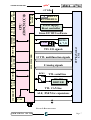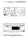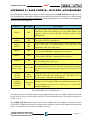
1
GMM ACB Zero
grifo® Mini Module AT89C51CC03
TECHNICAL MANUAL
Via dell'Artigiano, 8/6
® 40016 San Giorgio di Piano
(Bologna) ITALY
ITALIAN TECHNOLOGY
E-mail: [email protected]
http://www.grifo.it
http://www.grifo.com
Tel. +39 051 892.052 (a.r.) FAX: +39 051 893.661
grifo
GMM ACB Zero
Rel. 5.00
Edition 13 June 2007
®
®
, GPC , grifo , are trade marks of grifo®
GMM ACB Zero
grifo® Mini Module AT89C51CC03
TECHNICAL MANUAL
Male socket with 40 pins, dual in line, 100 mils pitch, 600 mils width; very small
dimension: 21 x 54 x 13 mm; 4 layers PCB to obtain best noisy resistance and
best EMI performance; requires single power supply at +5 Vdc, 48 mA;
availability of low power modes as Idle and Power Down; Atmel 89C51CC03
microcontroller (8051 code compatible) with 14.74 Mhz crystal; programmable
machine speed at 12 or 6 clock cycle; 64K FLASH for code, 2K FLASH for
Boot Loader, 256 bytes IRAM for data, 2K ERAM for data, 2K EEPROM for
data. Expansion signals for external memories and devices: up to 64K as data
access. 8 A/D converter channels with 10 bits resolution, 20 µsec conversion
time; 19 interrupt sources with 4 priority levels; 3 Timers Counters up to 16 bits;
5 PCA channels at 16 bits with PWM, compare, capture, etc. functionalities; 34
digital I/O lines available on connector; some of these have multifunctions
capabilities. Hardware serial line with Baud Rate programmable up to 115200
Baud, at TTL level or buffered in RS 232 with protection against ±15 KV
discharges. Reset and power supply control circuit. Software I2C BUS line,
available on connector; CAN controller compatible with 2.0A and 2.0B standards.
8 configuration Dip switches with 3 ways acquired by software; 2 signal LEDs
managed by software, through digital I/Os.
Internal FLASH and EEPROM can be managed through the In System
Programming, by using only the serial communication line, even when the
module is already mounted. Free software for PC that supports the ISP modality
in a fast and comfortable way. Wide range of development tools as: C compilers
(µC/51, HTC51, SYS51CW, DDS Micro C51); BASIC compilers (BASCOM
8051); PASCAL compilers (SYS51PW); Contact Logic (LADDER WORK);
etc. Long list of demo programs and use examples supplied under source (duly
remarked) and executable format, for the available development tools.
Via dell'Artigiano, 8/6
® 40016 San Giorgio di Piano
(Bologna) ITALY
ITALIAN TECHNOLOGY
E-mail: [email protected]
http://www.grifo.it
http://www.grifo.com
Tel. +39 051 892.052 (a.r.) FAX: +39 051 893.661
grifo
GMM ACB Zero
Rel. 5.00
Edition 13 June 2007
®
®
, GPC , grifo , are trade marks of grifo®
DOCUMENTATION COPYRIGHT BY grifo® , ALL RIGHTS RESERVED
No part of this document may be reproduced, transmitted, transcribed, stored in a
retrieval system, or translated into any language or computer language, in any form or
by any means, either electronic, mechanical, magnetic, optical, chemical, manual, or
otherwise, without the prior written consent of grifo®.
IMPORTANT
Although all the information contained herein have been carefully verified, grifo®
assumes no responsability for errors that might appear in this document, or for damage
to things or persons resulting from technical errors, omission and improper use of this
manual and of the related software and hardware.
grifo® reserves the right to change the contents and form of this document, as well as the
features and specification of its products at any time, without prior notice, to obtain
always the best product.
For specific informations on the components mounted on the card, please refer to the
Data Book of the builder or second sources.
SYMBOLS DESCRIPTION
In the manual could appear the following symbols:
Attention: Generic danger
Attention: High voltage
Attention: ESD sensitive device
Trade Marks
, GPC®, grifo® : are trade marks of grifo®.
Other Product and Company names listed, are trade marks of their respective companies.
grifo®
ITALIAN TECHNOLOGY
GENERAL INDEX
INTRODUCTION ........................................................................................................................ 1
VERSION ...................................................................................................................................... 3
NOTES ABOUT MINI MODULE NAME .............................................................................. 3
GENERAL INFORMATION ...................................................................................................... 4
SERIAL COMMUNICATION ................................................................................................. 5
DIGITAL I/O LINES................................................................................................................. 6
I2C BUS LINE ........................................................................................................................... 6
ANALOG INPUTS AND A/D CONVERTER ......................................................................... 6
MEMORY DEVICES................................................................................................................ 8
WATCH DOG ............................................................................................................................ 8
CLOCK ...................................................................................................................................... 8
BOARD CONFIGURATION ................................................................................................... 9
EXPANSION BUS ..................................................................................................................... 9
CAN CONTROLLER ............................................................................................................. 10
POSSIBLE APPLICATIONS ................................................................................................. 10
TECHNICAL FEATURES ........................................................................................................ 12
GENERAL FEATURES .......................................................................................................... 12
PHYSICAL FEATURES ......................................................................................................... 12
ELECTRIC FEATURES ........................................................................................................ 13
INSTALLATION ........................................................................................................................ 14
VISUAL SIGNALATIONS ..................................................................................................... 14
POWER SUPPLY .................................................................................................................... 14
CONNECTIONS ..................................................................................................................... 15
CN1 - CONNECTOR WITH MINI MODULE SIGNALS............................................... 16
RESET, POWER SUPPLY CONTROL, WATCH DOG ..................................................... 17
DIP SWITCH ........................................................................................................................... 18
INTERRUPTS ......................................................................................................................... 19
CONNECTOR SIGNALS INTERFACEMENT .................................................................. 20
SERIAL COMMUNICATION SELECTION ....................................................................... 20
OPERATING MODE SELECTION ..................................................................................... 22
EXTERNAL EXPANSIONS ................................................................................................... 22
CAN INTERFACE .................................................................................................................. 23
SUPPORT CARDS ..................................................................................................................... 24
USE WITH GMB HR168 MODULE..................................................................................... 24
USE WITH GMM TST AND GMM TST 2 BOARDS ......................................................... 26
HOW TO START ....................................................................................................................... 28
A) CONNECTIONS ARRANGEMENT ............................................................................... 28
B) TEST OF DEMO PROGRAM SAVED ON MINI MODULE ....................................... 29
C) FLASH REPROGRAMMING WITH DEMO PROGRAM .......................................... 29
GMM ACB Zero Rel. 5.00
Page I
grifo®
ITALIAN TECHNOLOGY
D) GENERATE EXECUTABLE CODE OF DEMO PROGRAM ..................................... 33
D3A) RECOMPILE WITH BASCOM 8051 ...................................................................... 33
D3B) RECOMPILE WITH µC/51 ...................................................................................... 35
D3C) RECOMPILE WITH LADDER WORK ................................................................. 38
E) FINAL PREPARATION OF APPLICATION ................................................................. 40
SOFTWARE DEVELOPMENT TOOLS ................................................................................. 42
PERIPHERAL DEVICES SOFTWARE DESCRIPTION ..................................................... 43
CONFIGURATION INPUTS ................................................................................................. 43
VISUALIZATION LEDS ........................................................................................................ 43
MULTIFUNCTIONS SIGNALS ............................................................................................ 44
MEMORY ACCESS ................................................................................................................ 44
BIBLIOGRAPHY ....................................................................................................................... 45
APPENDIX A: ON BOARD DEVICES DESCRIPTION .................................................... A-1
AT89C51CC03 ....................................................................................................................... A-1
APPENDIX B: GMM TST 2 ELECTRIC DIAGARAM ...................................................... B-1
APPENDIX C: BASE CONFIG., OPTIONS, ACCESSORIES ........................................... C-1
APPENDIX D: ALPHABETICAL INDEX ............................................................................ D-1
Page II
GMM ACB Zero Rel. 5.00
grifo®
ITALIAN TECHNOLOGY
FIGURES INDEX
FIGURE 1: LOCATION OF PRINTED CIRCUIT VERSION .......................................................................... 3
FIGURE 2: BLOCK DIAGRAM ............................................................................................................. 7
FIGURE 3: COMPLETE VIEW .............................................................................................................. 9
FIGURE 4: COMPONENTS MAP (TOP VIEW) ....................................................................................... 11
FIGURE 5: COMPONENTS MAP (BOTTOM VIEW) ................................................................................ 11
FIGURE 6: TOP VIEW ...................................................................................................................... 13
FIGURE 7: LEDS TABLE ................................................................................................................. 14
FIGURE 8: LEDS, DIP SWITCH, CONNECTOR LOCATION ................................................................... 15
FIGURE 9: CN1: SOCKET WITH MINI MODULE SIGNALS ................................................................. 16
FIGURE 10: DIP SWITCH TABLE (1 OF 2) ......................................................................................... 18
FIGURE 11: DIP SWITCH TABLE (2 OF 2) .......................................................................................... 19
FIGURE 12: TTL SERIAL LINE CONNECTION EXAMPLE ..................................................................... 21
FIGURE 13: RS 232 SERIAL LINE CONNECTION EXAMPLE ................................................................. 21
FIGURE 14: EXPANSION BUS FOR DATA AREA ................................................................................. 23
FIGURE 15: GMB HR168 + GMM ACB ZERO COUPLE .............................................................. 25
FIGURE 16: GMM TST + GMM ACB ZERO COUPLE .................................................................. 27
FIGURE 17: RS 232 SERIAL CONNECTION BETWEEN GMM ACB ZERO AND PC ............................ 28
FIGURE 18: DEMO PROGRAMS TABLE .............................................................................................. 30
FIGURE 19: FLIP SETTINGS WINDOW (1 OF 3) ................................................................................ 31
FIGURE 20: FLIP SETTINGS WINDOW (2 OF 3) ................................................................................ 31
FIGURE 21: FLIP SETTINGS WINDOWS (3 OF 3) .............................................................................. 32
FIGURE 22: LOAD SOURCE FILE WITH BASCOM 8051 .................................................................. 34
FIGURE 23: CONFIGURE COMPILER WITH BASCOM 8051 ............................................................ 34
FIGURE 24: COMPILE WITH BASCOM 8051................................................................................. 35
FIGURE 25: LOAD ENVIRONMENT FILE WITH µC/51 AND JFE ......................................................... 36
FIGURE 26: COMPILE WITH µC/51 AND JFE .................................................................................. 36
FIGURE 27: LOAD SOUCE FILE WITH µC/51 AND UEDIT .................................................................. 37
FIGURE 28: LOAD PROJECT FILE WITH µC/51 AND UMSHELL ......................................................... 37
FIGURE 29: COMPILE WITH µC/51 AND UMSHELL ......................................................................... 38
FIGURE 30: LOAD SCHEMATIC FILE WITH LADDER WORK ........................................................ 38
FIGURE 31: CONFIGURE COMPILER WITH LADDER WORK ........................................................ 39
FIGURE 32: COMPILE WITH LADDER WORK ............................................................................ 39
FIGURE 33: COMPILING RESULT WITH LADDER WORK ............................................................. 39
FIGURE 34: CONNECTION EXAMPLES .............................................................................................. 41
FIGURE C1: DEFAULT CONFIGURATION ......................................................................................... C-1
GMM ACB Zero Rel. 5.00
Page III
grifo®
Page IV
ITALIAN TECHNOLOGY
GMM ACB Zero Rel. 5.00
ITALIAN TECHNOLOGY
grifo®
INTRODUCTION
The use of these devices has turned - IN EXCLUSIVE WAY - to specialized personnel.
This device is not a safe component as defined in directive 98-37/CE.
Pins of module are not provided with any kind of ESD protection. Many pins of the card are directly
connected to their respective pins of on board's components and these last are sensitive to
electrostatic noises. So personnel who handles the product/s is invited to take all necessary
precautions that avoid possible damages caused by electrostatic discharges.
The purpose of this handbook is to give the necessary information to the cognizant and sure use of
the products. They are the result of a continual and systematic elaboration of data and technical tests
saved and validated from the manufacturer, related to the inside modes of certainty and quality of
the information.
The reported data are destined- IN EXCLUSIVE WAY- to specialized users, that can interact with
the devices in safety conditions for the persons, for the machine and for the enviroment, impersonating
an elementary diagnostic of breakdowns and of malfunction conditions by performing simple
functional verify operations, in the height respect of the actual safety and health norms.
The informations for the installation, the assemblage, the dismantlement, the handling, the adjustment,
the reparation and the contingent accessories, devices, installation, etc. are destined - and then
executable - always and in exclusive way from specialized warned and educated personnel, or
directly from the AUTHORIZED TECHNICAL ASSISTANCE, in the height respect of the
manufacturer recommendations and the actual safety and health norms.
The devices can't be used outside a box. The user must always insert the cards in a container that
rispect the actual safety normative. The protection of this container is not threshold to the only
atmospheric agents, but specially to mechanic, electric, magnetic, etc. ones.
To be on good terms with the products, is necessary guarantee legibility and conservation of the
manual, also for future references. In case of deterioration or more easily for technical updates,
consult the AUTHORIZED TECHNICAL ASSISTANCE directly.
GMM ACB Zero Rel. 5.00
Page 1
grifo®
ITALIAN TECHNOLOGY
To prevent problems during card utilization, it is a good practice to read carefully all the information
of this manual. After this reading, the user can use the general index and the alphabetical index,
respectly at the begining and at the end of the manual, to find information in a faster and more easy
way.
grifo® provid this documentation "as is" without warranty of any kind. In no event shall grifo® be
liable for indirect, special, incidental or consequential damages of any kind arising from any error
in this documentation, including any loss or interruption of business, profits, use , or data. Moreover
is not guaranteed the updating of the product for new computers or new operating systems, that will
become available in the future.
All trademarks listed in this manual are copyright of the relative manufacturers.
Page 2
GMM ACB Zero Rel. 5.00
grifo®
ITALIAN TECHNOLOGY
VERSION
This handbook make reference to printed circuit version 140207 and following ones. The validity
of the information contained in this manual is subordinated to the version number on the used card,
and so the user must always verify the correct correspondence between the notations. The version
number is reported in several places on the electronic part of the product, and following figure shows
the most accessible one.
PRINTED CIRCUIT
version
FIGURE 1: LOCATION OF PRINTED CIRCUIT VERSION
NOTES ABOUT MINI MODULE NAME
Please note that near the printed circuit revision number, just described, the card name is GMM ACB.
In fact GMM ACB Zero is realized by using the GMM ACB printed circuit where it is mounted an
89C51CC03 microcontroller.
In order to distinguish GMM ACB and GMM ACB Zero it is necessary to check the component
installed on IC3 and then use the following corrispondence:
Mounted microcontroller
Atmel 89C51CC03
Atmel 89C51AC2
GMM ACB Zero Rel. 5.00
->
->
->
Module name
GMM ACB Zero
GMM ACB
Page 3
grifo®
ITALIAN TECHNOLOGY
GENERAL INFORMATION
GMM ACB Zero is a Mini Module based on microcontroller Atmel 89C51CC03, that is a powerful
and complete system on chip provided with CPU, internal memories and a rich list of peripherals
suitable for typical requirements of automation applications.
The module has already mounted inside its reduced size the components that exploit the main features
of microcontroller and allows the use of all the operating modes; furtermore it includes some other
components that simplify and increase the application fields.
GMM ACB Zero can be used for many installations either in the industrial, domestic, automotive
and didactic environments, as described in following paragraphs.
The card use is simplified by a wide range of software developement tools based either on low or high
level programming languages which allow to work at the best conditions using only a standard PC.
Noteworthy among these tools there are the C, PASCAL, BASIC compilers and a graphic
programming environment based on logic contact (LADDER). Special care has been devoted to the
application developing, by selecting tools which allow on board FLASH burning with user
application program and remote debug directly on the card, always with the simple use of a standard
PC.
The GMM ACB Zero is equipped with a normalized standard connector that allows immediate
mounting on support cards as GMM TST 2, GMB HR168 and GMB HR246 or mounted directly
on a board developed by the user, as a macro component. Both the solutions ensure a short time to
market: the user can obtain a prototype or even a ready product in one week.
Overall features of GMM ACB Zero are:
- Standard format with 40 pins male socket, Dual In Line, 100 mils pitch, 600 mils width.
- Very small dimension: 21 x 54 x 13 mm.
- 4 layers printed circuit board to obtain best noisy resistance and best EMI performances.
- Single power supply required +5 Vdc (the current consumption may vary according to
module connections and status).
- Availability of low consumtion modality as Idle and Power Down Modes.
- Atmel 89C51CC03 microcontroller (8051 code compatibile) with 14.74 MHz crystal.
- Programmable machine speed at 12 or 6 clock cycle.
- 64K FLASH for code, 2K FLASH for Boot Loader, 256 bytes IRAM for data, 2K
ERAM for data, 2K EEPROM for data.
- Expansion signals for external devices addressed as data.
- As external expansion can be easily connected up to 64K of SRAM.
- 8 A/D converter channels with 10 bits resolution, 20 µsec conversion time.
- 19 interrupt sources with 4 priority levels.
- 3 Timers Counters up to 16 bits.
- 5 PCA channels up to 16 bits with PWM, compare, capture on event, frequency
generator, etc. functionalities.
- Watch dog section that ensure right work of the controlled system in any operating
conditions.
- 34 digital I/O lines available on connector. Some of these have multiple functions.
- Hardware serial line with programmable Baud Rate up to 115200 Baud, at TTL level
or RS 232 buffered.
- RS 232 driver with protection against ±15 kV discharges.
- Reset and power supply control circuit.
Page 4
GMM ACB Zero Rel. 5.00
ITALIAN TECHNOLOGY
grifo®
- Software I2C BUS line, available on connector.
- CAN controller compatible with 2.0A and 2.0B standards that can be connected to each
line based on this protocol, through a proper external driver.
- 8 configuration Dip switches; 3 of them can be acquired by software.
- 2 status LEDs managed by software through I/O lines.
- Internal FLASH and EEPROM can be managed through ISP (In System Programming),
that is with the module already mounted, by using only the serial communication line.
- Free software for PC, that supports the ISP programmation of the generated code, inside
the on board FLASH.
- Wide range of development tools that requires only a standard PC. Among the most
diffused there are: C compilers (µC/51, MCC51, HTC51, SYS51CW, DDS Micro C51);
BASIC compiler (BASCOM 8051); PASCAL compiler (SYS51PW); language with
contact logic (LADDER WORK); etc.
- Long list of demo programs and user examples supplied under source form, duly
remarked, for the available development tools.
Here follows a description of the board's functional blocks, with an indication of the operations
performed by each one. To easily locate such sections and verify their connections please refer to
figure 2.
SERIAL COMMUNICATION
On GMM ACB Zero it is always available an hardware serial line that is completely software
configurable for physical protocol (baud rate, stop bits number, lenght of character, etc) by simply
programming some microprocessor's internal registers.
The serial line is connected to CN1 connector at TTL or RS 232 level, thanks to some on board Dip
switches for configuration. When the card must be connected in a network or at long distance or with
other systems that use different electric protocols, the user must provide proper external drivers (i.e.
RS 232,RS 422, RS 485, Current Loop, etc.). In addition to standard receive and transmit signals on
CN1 connector there are also other I/O signals that can be driven by software; these signals can be
used to define the RS 485 line direction, to enable the RS 422 transmit drive or to generate the
RS 232 hardware handshakes. For example the MSI 01 module can convert a TTL serial line in any
other electric standards, in a pratical and inexpensive way.
Please read SERIAL COMMUNICATION SELECTION paragraph of this manual or contact
directly grifo® technicians, for further explanations or any other necessary information about
electric protocols. Viceversa please read the manufacturer documentation in APPENDIX A of this
manual and the numerous supplied examples, for detailed description of the internal registers that
defines physical protocol and manages basic aspects of communication.
As described in following pages it is important remind that the module supports also other different
types of serial communication, as the I2C BUS and the CAN BUS.
GMM ACB Zero Rel. 5.00
Page 5
grifo®
ITALIAN TECHNOLOGY
DIGITAL I/O LINES
The Mini Module GMM ACB Zero provides 34 digital I/O lines at TTL level, of the microprocessor
Atmel 89C51CC03, grouped in four 8 bits ports (P0, P1, P2 and P3) and in one 2 bits port (P4). A
standard rules defines the names of all the signals on the Port as P0.0÷7, P1.0÷7, P2.0÷7, P3.0÷7 and
P4.0÷1.
These lines are connected directly to 40 pins connector with a standard pin out, common for all the
grifo® Mini Module, by allowing a direct connection to several interface cards.
By software it is possible to define and acquire the function, the direction and the status of these lines,
and also to match them to peripheral devices (i.e. Timer, Counter, Interrupt, A/D, PCA, CAN
controller, etc.), through a simple programming of some microcontroller internal registers.
For further information please refer to paragraph CONNECTIONS and PERIPHERAL DEVICES
SOFTWARE DESCRIPTION.
I2C BUS LINE
On standard connector of GMM ACB Zero there are the signals of an I2C BUS interface emulated
by software, and managed by two I/O lines of microcontroller.
This interface allows to connect the devices featuring the same communication standard in order to
expand local potentialities of module.
There is wide range of software examples that manage most common devices with I2C BUS interface
like A/D and D/A converters, display drivers, memories, temperature sensors, etc.
If you are intrested in this interfaces, it can be useful to consider the K51-AVR card, for which both
technical manual featuring electric diagram and a complete set of examples programs are available.
In addition remind also some models of QTP operator panel that can be driven with an I2C BUS line
as an alternative to asynchronous communication line.
ANALOG INPUTS AND A/D CONVERTER
Mini Module GMM ACB Zero provides 8 analog inputs connected to A/D converter section of
microcontroller. These inputs can be connected to external sensors that convert many physic
quantities (as temperature, pressure, speed, weight, etc.) or any other system that supplies a
compatible voltage signal.
Main feautes of this section are: resolution 10 bits, 8 indipendent analog inputs, maximum accepted
range 0÷3 V, conversion time on a single channel 20 µsec, very easy software management, end of
conversion interrupt.
A/D conversions are performed using the successive approximations technique and are made
through opportune manipulation of specific microcontroller internal registers.
In order to simplify the A/D converter management, some software packages are provided with
specific procedures that manage all details of this section.
For further information please refer to data sheet of APPENDIX A of this manual or paragraph
CONNECTIONS.
Page 6
GMM ACB Zero Rel. 5.00
grifo®
ITALIAN TECHNOLOGY
INTERRUPT
2K BOOT
LOADER
DSW1.1
RUN/DEBUG
Power supply,
Reset controller
Linea I2C BUS software
DSW1.
6, 7, 8
LED
MULTIPLEXER
TTL I/O signals
12 TTL multifunction signals
40 Pins Socket
CN1
CPU
AT89C51CC03
2K
64 K 2,2 K
WATCH UART
PCA: PWM, PORT I/O TIMER/
A/D
DOG
COUNTER
COUNTER FLASH RAM EEPROM
+5 Vdc
8 Analog signals
DSW1
TTL serial line
RS 232
DRIVER
TTL CAN line
ALE, /PSEN for expansions
CAN
FIGURE 2: BLOCK DIAGRAM
GMM ACB Zero Rel. 5.00
Page 7
grifo®
ITALIAN TECHNOLOGY
MEMORY DEVICES
The card is provided of 70.25K of memory divided in the following types:
- 64K Bytes of FLASH EPROM;
- 2K Bytes of FLASH EPROM for Boot Loader;
- 256 Bytes of internal IRAM;
- 2K Bytes of external ERAM;
- 2K Bytes of EEPROM.
All these memories, except the FLASH for Boot Loader, are completely available for user
requirements, both for code and data of his application program.
Thanks to on board EEPROM there is the possibility to keep data also when power supply is failed;
in this way the card is always able to maintain parameters, logged data, system status, configurations
and so on, in each working conditions.
Whenever the amount of memory for data is not sufficient (i.e. for data loghin systems or special
applications), it is always possible to connect external memory devices (with SRAM, EEPROM,
FLASH, EPROM technologies) through the efficient expansion BUS and/or the comfortable I2C
BUS interface of the card (please see propers paragraphs).
The addressing and management of memory devices is controlled by microcontroller as described
in paragraph MEMORY ACCESS and inside the component data sheet or in APPENDIX A of this
manual.
WATCH DOG
Microcontroller 89C51CC03 includses an hardware Watch Dog capable to reset the CPU if the user
program doesn't retrigger it before than the selected intervent time elapses. The main purpose of this
section is to supply a real security to the system controlled by Mini Module in order to work correctly
in any operating conditions and to avoid dangerous malfunctions not examined during develop
phase.
The intervent time rangeof Watch Dog is rather wide, from a minimum of about 6 millisecond to a
maximum of 1.7 second.
For further information refer to microcontroller data sheet or to APPENDIX A of this manual.
CLOCK
On GMM ACB Zero module there is one clock circuitery that generates the clock signal for the
microcontroller. Such circuitery is based on a crystal that generates a 14.7456 MHz frequency that
is used, directly or indirectly, by all the peripherals of the module that requires timings as the
asynchronous serial line, the Timers, the Watch Dog, the PCA channel, etc.
In order to improve speed performance, on GMM ACB Zero the user can also set the machine cycle
duration to 12 or 6 clock cycles (X2 mode). In X2 mode code execution is two times faster than a
classic 8051 architecture.
Page 8
GMM ACB Zero Rel. 5.00
ITALIAN TECHNOLOGY
grifo®
BOARD CONFIGURATION
The GMM ACB Zero is provided with a Dip switch with 8 ways that allow to configure the module
and its application program. Three of these dips can be acquired by software and they let the user
manages different conditions through a single program, with no renounce to other input lines (the
typical applications are: languages selection, definition of program parameters, operating modes
selection, etc.).
Moreover one dip is used at power on or after a reset to determine which working modality, RUN
or DEBUG, is used, that is respectively, whether the microcontroller has to run the user application
program or the Boot Loader.
In addition, the board is also provided with two signalation LEDs; these are software manageable,and
can be used to signal the board status and configurations in a visual ways , as described in the specific
paragraphs.
All the configuration resources described are completely software manageable by simply using few
specific registers of the microcontroller.
For further information refer to paragraphs DIP SWITCH, VISUAL SIGNALATIONS and
VISUALIZATION LEDS.
EXPANSION BUS
The GMM ACB Zero is provided of an interesting and innovative feature for grifo® Mini Module
that is the possibility to obtain an expansion BUS. By connecting some of the signals on CN1
connector to a very simple external circuit, you obtain a real parallel BUS with 8 bits, complete of
data, addresses and control lines.
As described in EXTERNAL EXPANSIONS paragraph with this feature can be connected either
parallel memories and/or numerous I/O peripherals, by obtaining an extraordinary enlargement of
the potentialities and possible application fields of the module.
FIGURE 3: COMPLETE VIEW
GMM ACB Zero Rel. 5.00
Page 9
grifo®
ITALIAN TECHNOLOGY
CAN CONTROLLER
The CAN controller of GMM ACB Zero is charged of the complete management of the homonimous
protocol in all its modalities and aspects. In details the overall features of this section are briefly
described below:
- supports for BasicCAN protocol (2.0 A);
- supports for PeliCAN protocol (2.0 B);
- identifiers lenghts supported: 11 and 29 bits;
- 15 indipendent messages managers;
- separated identifiers, masks and commands for each manager;
- programmable receive buffer size;
- programmable timer for triggers and synchronizations;
- readable errors counters;
- generates some different interrupts according with current controller status;
- completely managed through microcontroller's internal registers;
- etc.
For further information please refer to CAN INTERFACE paragraph and to APPENDIX A of this
manual.
POSSIBLE APPLICATIONS
Possible applications of GMM ACB Zero modules are several. The following example can be listed:
- Smart intelligent nodes with local functionalities as PID algorithms for controlling temperatures,
motors, valves, etc.
- Decentralized systems as robots, automation of production line machines, big factory automations,
etc.
- Teleacquisition and telecontrol on medium and low distances.
- Application in home automation where it performs tasks like lights turning ON/OFF, heating and
cooling systems control, supervision of electric devices, security and acces control systems,
gardens sprinkle, etc.
- Car automations (automotive) as lights turning ON/OFF, heating and cooling systems control,
supervision services for drivers, anti-teft and acces control systems, functionality checks, etc.
- Also the CAN applications are possible, but only when the Mini Module is integrated with an
external line driver. So it can be used again in automotive applications, in the connection to CAN
networks based on propietary protocols or standard protocols as CANopen, DeviceNet, SDS, CAN
Kingdom J1939, etc.
- Last but not least, the didactics use in fact GMM ACB Zero offers a very low cost system suitable
to learn microcontroller with famous 8051 core and to develop the typical start applications for the
students. For this purpose it is likewise interesting the GMM TST or GMM TST 2 support cards
that solve the problems of power supply, of serial connection to development PC and of module
lines connection. In the same support cards there are a matrix keyboard and a LCD display that allow
to study and test some low cost user interface solutions.
- All the applications where it is necessary to reduce developing time and price: in fact the module
can be mounted directly on the board developed by the user, as a ready to use macro component.
Page 10
GMM ACB Zero Rel. 5.00
grifo®
ITALIAN TECHNOLOGY
FIGURE 4: COMPONENTS MAP (TOP VIEW)
FIGURE 5: COMPONENTS MAP (BOTTOM VIEW)
GMM ACB Zero Rel. 5.00
Page 11
grifo®
ITALIAN TECHNOLOGY
TECHNICAL FEATURES
GENERAL FEATURES
Devices:
34 lines of TTL digital I/O
8 analog inputs on A/D converter
5 PCA sections for compare, capture, PWM, frequency signals
1 Watch Dog section
3 Timers, Counters multifunctions
19 interrupt sources with 4 levels
1 reset and power supply controller circuit
1 RS 232 or TTL serial line
1 CAN controller
1 Dip switch with 8 ways
2 visualization LEDs
Memories:
64K Byte FLASH
2K Byte FLASH
2K Byte EEPROM
2K Byte ERAM
256 Bytes IRAM
Microcontroller:
Atmel 89C51CC03
Clock frequency:
14.7465 MHz
A/D resolution:
10 bits
A/D conversion time:
20 µsec
Reset time:
typical 200 msec
Watch Dog intervent time:
programmable from about 6 msec to 1.7 sec
user program
boot loader
user data (last 8 Bytes are reserved)
user data
user data
PHYSICAL FEATURES
Size:
21 x 54 x 13 mm
Weight:
9g
Connectors:
CN1: 40 pins male socket DIL,100 mils pitch, 600 mils width.
Temperature range:
0÷50 °C
Relative humidity:
20%÷90%
Page 12
(without condense)
GMM ACB Zero Rel. 5.00
grifo®
ITALIAN TECHNOLOGY
ELECTRIC FEATURES
Power supply voltage:
+5 Vdc ± 5%
Current consumption:
48 mA
64 mA
Analog inputs voltage range:
0÷Vref
A/D reference voltage Vref:
0÷3 V
Analog inputs impedance:
high
Power failure theshold:
typical 4.65 Vdc
RS 232 protection:
±15 KV
(*)
*
*
(normal)
(maximum)
The reported values are referred to 20 C° environment temperature (for further information
please refer to chapter POWER SUPPLY).
FIGURE 6: TOP VIEW
GMM ACB Zero Rel. 5.00
Page 13
grifo®
ITALIAN TECHNOLOGY
INSTALLATION
In this chapter there are the information for a right installation and correct use of the card GMM ACB
Zero. In detail there are the locations and functions of each connector, of the user settable Dip
switches, LEDs, and so on.
VISUAL SIGNALATIONS
GMM ACB Zero is provided of the LEDs described in the following table:
LED
COLOUR
FUNCTION
LD1
Green
When lighted, indicates that signal P2.6 (pin 5 of Mini Module) is at
low level (zero volt) or that DSW1.7 is in ON position.
LD2
Red
When lighted, indicates that signal P2.7 (pin 6 of Mini Module) is at
low level (zero volt) or that DSW1.6 is in ON position.
FIGURE 7: LEDS TABLE
The main function of LEDs is to inform the user about card status, with a simple visual indication
and in addition to this, LEDs make easier the debug and test operations of the complete system.
To recognize the LEDs location on the card, please refer to figure 8, while for further information
about management, please refer to paragraph VISUALIZATION LEDS.
POWER SUPPLY
Mini Module nust be supplied with a stabilized +5 Vdc ± 5% voltage connected to proper pins 20
and 34 of CN1.
On the board all the circuits and components have been chosen in order to obtain the best noisy
immunity and the lowest consumption, including the possibility to use some different low power
modalities; this feature is really important when the module is supplied by batteries for example in
portable applications. In details it can be set the power down and the idle modes plus the machine
cycle speed of the microcontroller, through the proper internal register PCON. The user application
program can reduce supply consumption and eventually restore the normal working mode when a
specific event occours, like an interrupt, a variation on an analog or digital input, a timeout, etc.
For further information please refer to paragraph ELECTRIC FEATURES.
Page 14
GMM ACB Zero Rel. 5.00
grifo®
ITALIAN TECHNOLOGY
LD1
DSW1
CN1
LD2
FIGURE 8: LEDS, DIP SWITCH, CONNECTOR LOCATION
CONNECTIONS
The GMM ACB Zero module has 1 connector that can be linkeded to other devices or directly to
the field, according to system requirements.
In this paragraph there are connector pin out, a short signals description (including the signals
direction) and connectors location (see figure 8) that simplify and speed the installation phase.
Some additional figures shows the pins functionalities and some of the most frequently used
connections.
All the connectors of grifo® cards follows standard pin outs in order to obtain a modular electronics
where each cards can be changed with many others, of the same or different type. This reduces times
and costs when modules become obsolete or insufficient for the application requirements.
GMM ACB Zero Rel. 5.00
Page 15
grifo®
ITALIAN TECHNOLOGY
CN1 - CONNECTOR WITH MINI MODULE SIGNALS
CN1 is a 40 pins, male, dual in line, socket connector with 100 mils pitch and 600 mils width.
On this connector are available all the interfacement signals of the Mini Module as the power supply,
the I/O lines, the asynchronous and synchronous communication lines, the on board peripheral
devices signals, the expansion signals, etc.
Many pins of the connector have multiple functions in fact, by software, some internal sections of
microcontroller can be multiplexed with I/O signals and the following figure list all these possible
functionalities. So the signals available on CN1 have different characteriistics, as described in the
following CONNECTOR SIGNALS INTERFACEMENT paragraph, and they follow grifo® Mini
Module standard pin out.
In order to avoid problems on pin counting and numbers the figure 9 shows the signals directly on
the top view of the GMM ACB Zero; moreover the serigraph reports the pins number on the four
corners of the card both on bottom and top side.
AD0 , P0.0
AD1 , P0.1
AD2 , P0.2
AD3 , P0.3
DSW1.7 , LD1 , A14 , P2.6
DSW1.6 , LD2 , A15 , P2.7
Vref
/RES
RX RS232 , RX TTL , P3.0
TX RS232 , TX TTL , P3.1
DSW1.8 , A13 , P2.5
SCL , A8 , P2.0
SDA , A9 , P2.1
TxD CAN , P4.0
RxD CAN , P4.1
A12 , P2.4
A11 , P2.3
A10 , P2.2
/RD , P3.7
GND
1
2
3
4
5
6
7
8
9
10
11
12
13
14
15
16
17
18
19
20
40
39
38
37
36
35
34
33
32
31
30
29
28
27
26
25
24
23
22
21
/PSEN
ALE
P0.7 , AD7
P0.6 , AD6
P0.5 , AD5
P0.4 , AD4
+5 Vdc
P1.0 , AN0 , T2
P1.1 , AN1 , T2EX
P1.2 , AN2 , ECI
P1.3 , AN3 , CEX0
P1.4 , AN4 , CEX1
P1.5 , AN5 , CEX2
P1.6 , AN6 , CEX3
P1.7 , AN7 , CEX4
P3.2 , /INT0
P3.3 , /INT1
P3.4 , T0
P3.5 , T1
P3.6 , /WR
FIGURE 9: CN1: SOCKET WITH MINI MODULE SIGNALS
Signals description:
RX RS232
TX RS232
RX TTL
TX TTL
Px.n
DSW1.n
LDn
/INTn
Tn
T2EX
SCL
SDA
Page 16
= I - Receive Data of serial line buffered in RS 232
= O - Transmit Data of serial line buffered in RS 232
= I - Receive Data of TTL serial line
= O - Transmit Data of TTL serial line
= I/O - Signal n of Port x of microcontroller digital I/Os
= O - Signal connected to contact n of Dip switch DSW1, that short circuit to
ground
= O - Signal connected to visualization LED LDn
= I - Interrupt lines n of microcontroller
= I - Signal connected to section Timern of microcontroller
= I - External trigger signal for Ttimer 2
= I/O - Clock lines of software I2C BUS interface
= I/O - Data lines of software I2C BUS interface
GMM ACB Zero Rel. 5.00
ITALIAN TECHNOLOGY
RxD CAN
TxD CAN
Vref
ANn
CEXn
ECI
ADn
An
/WR
/RD
/PSEN
ALE
/RES
+5 Vdc
GND
grifo®
= I - Receive Data of CAN controller
= O - Transmit Data of CAN controller
= I - A/D converter reference voltage
= I - Analog inputs connected to A/D converter section
= I/O - Signal connected to section PCAn (PWM outputs, capture and compare
inputs, etc.)
= I - External clock signal of PCA sections
= I/O - Low addresses signals and data signals of expansion BUS
= O - High addresses signals of expansion BUS
= O - Write signal for data area of expansion BUS
= O - Read signal for data area of expansion BUS
= O - Read signal for code area of expansion BUS
= O - Latch signal for low addresses of expansion BUS
= I - Reset signal
= I - +5 Vdc power supply voltage
=
- Ground
RESET, POWER SUPPLY CONTROL, WATCH DOG
On GMM ACB Zero are available three different reset sources, that can be so summarized:
1) Power supply control circuit that enables the reset when the power supply voltage decreases down
to the 4.65 Vdc threshold.
2) Signal connected to pin 8 of CN1, active low, that can be connected to a simple normally open push
button; once the button is pressed it must short circuit the /RES signal to ground GND and
consequently the reset is enabled. The main purpose of this signal is the forced exit from endless
loop, especially during the debug phase, or the re-execution of the application program with no
interruptions on the power supply of the card.
3) Watch Dog circuit, inside the microcontroller, that is really efficient and easy to use by software.
In details the main features of this circuit are the following ones:
- astable functionality;
- intervent time programmable by software from about 6 msec to about 1700 msec;
- software enable through a double consecutive write operation on management registers;
- software retrigger.
In astable mode when intervent time is elapsed the circuit becomes active, it stays active for a short
reset time and after it is deactivated. The main purpose of this section is to supply a real security
about right execution of application program by the card. In fact when the program is no more
executed correctly, it doesn't perform the periodic retrigger operation of the circuit and the card
will be reset at the end of intervent time. For further information about Watch Dog section and
retrigger operation, please refer to the microcontroller data sheet or APPENDIX A of this manual.
For the first two sources, the reset circuit stays enabled for the reset time (about 200 msec) and then
it is disabled, while for the third source it is enabled only for few µsec. At this point all the sections
of the card are reset, in order to warrant a complete reset status, and it resumes execution of the
program stored on FLASH, at the address 0000H.
The reset circuit with these features ensures the right functionality of the card and of all the possible
connected electronics, in each working condition and especially during the dangerous and difficult
phases of power on and power off.
GMM ACB Zero Rel. 5.00
Page 17
grifo®
ITALIAN TECHNOLOGY
DIP SWITCH
On GMM ACB Zero module there is an 8 ways Dip switch, named DSW1, that defines some
configurations of the card. In the following figures is reported their list and their functions in all the
available connection modes.
SWITCH
POSITION
ON
1
OFF
ON
2
OFF
ON
3
OFF
FUNCTION
DEF.
Connects /PSEN signal of microcontroller to ground (zero
volt). When Mini Module is turned on or reset in this
condition, DEBUG mode is enabled and Boot Loader runs.
Does not connect /PSEN signal of microcontroller. When
Mini Module is turned on or reset in this condition, RUN
mode is enabled and the program saved in microcontroller
FLASH memory, runs.
Connects transmission signal, on pin 10 of CN1, to RS 232
serial driver. DSW1.4 must be OFF to avoid conflicts. Used
in conjunction with switches 3, 4, 5.
Does not connect transmission signal, on pin 10 of CN1, to
RS 232 serial driver, by allowing direct connection to
microcontroller.
Connects reception signal, on pin 9 of CN1, to RS 232 serial
driver. DSW1.5 must be OFF to avoid conflicts. Used in
conjunction with switches 2, 4, 5.
Does not connect reception signal, on pin 9 of CN1, to
RS 232 serial driver, by allowing direct connection to
microcontroller.
ON
Connects transmission signal, on pin 10 of CN1, directly to
microcontroller. DSW1.2 must be OFF to avoid conflicts.
Used in conjunction with switches 2, 3, 5.
OFF
Does not connect transmission signal, on pin 10 of CN1,
directly to microcontroller, by allowing the connection to
RS 232 serial driver.
ON
Connects reception signal, on pin 9 of CN1, directly to
microcontroller. DSW1.3 must be OFF to avoid conflicts.
Used in conjunction with switches 2, 3, 4.
4
5
OFF
ON
6
OFF
Does not connect reception signal, on pin 9 of CN1, directly
to microcontroller, by allowing the connection to RS 232
serial driver.
Connects pin 6 of Mini Module to ground. This condition
forces the P2.7 signal of microcontroller to 0 logic level,
and it acts as a configuration input acquired by software.
Furthermore it enables the LED LD2.
Does not connect pin 6 of Mini Module and it lets the signal
P2.7, and the LED LD2, completely driven by user.
*
*
*
*
*
*
FIGURE 10: DIP SWITCH TABLE (1 OF 2)
Page 18
GMM ACB Zero Rel. 5.00
grifo®
ITALIAN TECHNOLOGY
SWITCH
POSITION
FUNCTION
DEF.
Connects pin 5 of Mini Module to ground. This condition
forces the P2.6 signal of microcontroller to 0 logic level,
and it acts as a configuration input acquired by software.
Furthermore it enables the LED LD1.
Does not connect pin 5 of Mini Module and it lets the
signal P2.6, and the LED LD1, completely driven by
user.
ON
7
OFF
Connects pin 11 of Mini Module to ground. This
condition forces the P2.5 signal of microcontroller to 0
logic level, and it acts as a configuration input acquired
by software.
Does not connect pin 11 of Mini Module and it lets the
signal P2.5 completely driven by user.
ON
8
OFF
*
*
FIGURE 11: DIP SWITCH TABLE (2 OF 2)
In the previous tables the * (asterisk) denotes the default connection, or on the other hand the
connection set up at the end of testing phase, that is the configuration the user receives. The user can
check the base configuration originally received, also in APPENDIX C of the manual.
In order to locate the Dip switch, please refer to figure 8.
INTERRUPTS
One of the most important GMM ACB Zero features is the powerful interrupts management. Below
there is a short description of which devices can geneate interrupts and their modalities; for further
information about interrputs management please refer to the microcontroller data sheet or APPENDIX
A of this manual.
- Pin 25 of CN1
- Pin 24 of CN1
- Peripheral devices
->
->
->
Generates /INT0 = P3.2 on the microcontroller.
Generates /INT1 = P3.3 on the microcontroller.
Generate an internal interrupt. Possible sources of internal interrupts
are the sections: Timer 0, Timer 1, Timer 2, PCA, UART, A/D
converter, CAN controller, CAN timer, etc.
An interrupt management section, integrated in microcontroller, allows to enable, disable, mask and
prioritize, so the user has the possibility to service promptly and efficently any external event. The
same interrupt section let the user manage the 19 interrupt sources with 4 priority levels; the addresses
of the interrupt service routines can be software programmed by the user placing them on the proper
code area; viceversa the interrupts priority level and activation are sofware programmable through
specific internal registers. So the application program can always react promptly to every events, by
defining also the priority of contemporaneous interrupts.
GMM ACB Zero Rel. 5.00
Page 19
grifo®
ITALIAN TECHNOLOGY
CONNECTOR SIGNALS INTERFACEMENT
In order to prevent possible connecting problems between GMM ACB Zero and the external
systems, the user has to respect carefully all the indications and figures of the manual and he must
follow these instructions:
- For RS 232 signals the user must follow the standard specifications of this protocol, defined by
CCITT normatives.
- All TTL signals must follow the rules of this electric standard. The connected digital signals must
be always referenced to card ground (GND) and then the 0V level corresponds to logic status 0,
while the 5V level corresponds to logic status 1. The connection of these lines to devices of the
controlled system (encoders, switches, proximity, electric valves, relays, motors, etc.) must be
performed through proper power interfaces; it is preferible to adopt opto coupled interfaces that
ensure an electric insulation between Mini Module electronic and external noisy, typically
generated by power electronic.
- The inputs for analog section must be connected to low impedance signals in the range 0÷3.0 V,
that assure greater stability and precision. This range is valid also for the reference voltage Vref,
used by A/D section, that must be perfectly filtered and stabilized.
- The PWM signals generated by Timer, Counter and PCA sections are TTL type so they must be
properly buffered in order to drive the power circuitery. Typical interfaces can be a simple current
driver (when a PWM signal is still required) or an intergrator circuit, when analog voltage is
necessary.
- Also I2C BUS signals are at TTL level, as defined by the same standards; for completeness it is
remarked that in a network with several devices and rather long, it is better to study the connection
lay out and to set properly the output stage, the operational modes and the programmable bit rate:
the best values of all these settings allow right communications in any condition. Each I2C BUS
connection must have two pull up resistors at the extremes of the cable, that is near the two units
at the greatest distance, as defined by standard specification of this interface.
- The CAN communication signals are at TTL level and they can't be directly connected to signals
of the CAN lines, but it must be interposed a proper line driver, as described in paragraph CAN
INTERFACE.
SERIAL COMMUNICATION SELECTION
Asynchronous serial line of GMM ACB Zero can be buffered in RS 232 or TTL. In case it is buffered
in RS 232, the line signals are protected against discharges up to ±15 KV.
By software the serial line can be programmed to operate with all the standard physical protocols,
in fact the bits per character, parity, stop bits and baud rates can be defined by setting proper
microprocessor's internal registers.
By hardware can be selected which one of the electric protocols is used, through Dip switches
configuration, as described in the previous tables; the user can select autonomously one or the other
type by following the information listed below. Moreover the following figures shows how a generic
external system can be connected to GMM ACB Zero serial line, with both the electric standards.
Page 20
GMM ACB Zero Rel. 5.00
grifo®
ITALIAN TECHNOLOGY
- SERIAL LINE IN TTL
=
=
=
=
OFF
OFF
ON
ON
RX TTL
TX
TX TTL
RX
9
10
GND
External System
CN1 GMM ACB Zero
DSW1.2
DSW1.3
DSW1.4
DSW1.5
GND
20
FIGURE 12: TTL SERIAL LINE CONNECTION EXAMPLE
- SERIAL LINE IN RS 232 (default configuration)
=
=
=
=
ON
ON
OFF
OFF
RX RS232
TX
TX RS232
RX
9
10
GND
External System
CN1 GMM ACB Zero
DSW1.2
DSW1.3
DSW1.4
DSW1.5
GND
20
FIGURE 13: RS 232 SERIAL LINE CONNECTION EXAMPLE
GMM ACB Zero Rel. 5.00
Page 21
grifo®
ITALIAN TECHNOLOGY
OPERATING MODE SELECTION
As described on figure 10 and in next chapters, the Dip switch DSW1.1 selects the operating mode
of GMM ACB Zero Mini Module. In detail are available two modes obtained from the following
configurations:
DSW1.1
OFF
ON
->
->
Operating mode
RUN mode
DEBUG mode
In RUN mode after a reset or power on the application program saved in FLASH is always executed,
independently by external conditions, while in DEBUG mode the Boot Loader of microcontroller
is always executed.
Programs for PC, as the FLIP, comunicates with Boot Loader through the serial line and allow to read,
erase and write some on board memories through the ISP modality.
The ISP tecnique (In System Programming) reduces the cost and the time for development in fact
it eliminates the use of external EPROMs, programmer, eraser, etc. For further information about ISP
please consult the specific technical documentation released by ATMEL.
EXTERNAL EXPANSIONS
On CN1 connector are available all the signals required to obtain a BUS external to Mini Module
that allows the connection of many devices and thus to expand the resources and the functionalities
of GMM ACB Zero.
The most important features of the expansion BUS are listed in the following points:
- parallel BUS type.
- Provided of 8 data bits and 16 address bits.
- Complete of control signals required either for acces on data area and code area, according with
typical modalities of microcontroller.
- Maximum address spaces: 64K Bytes only in data area in fact the code area is completely used by
the 64K Bytes of the on board FLASH.
- Very simple interfacement circuit that normally requires a single latch (for example a 74HCT573
component) that memorizes the low part of the addresses multiplexed with data.
- Suitable for connection of external parallel memories as SRAM, EPROM, FLASH EPROM,
EEPROM.
- Suitable for connection of all the external peripherals provided of a parallel BUS, as digital I/O
controllers, A/D converters, D/A converters, serial communication controllers (CAN, USB,
asynchronous serial lines, etc.), hardware counters, etc.
- The expansion BUS can be easily used to realize a standard ABACO® I/O BUS interface that allows
an istantaneous connection to the wide range of grifo® peripheral cards, ready to use.
- Simple software management of the expansion BUS that is addressed with all the instrunctions for
external memory access provided by the microcontroller or by the selected programming language.
Page 22
GMM ACB Zero Rel. 5.00
grifo®
ITALIAN TECHNOLOGY
The block diagaram of the following figure shows how the expansion BUS can be realized in a
simplified mode, for the available addressable area.
FIGURE 14: EXPANSION BUS FOR DATA AREA
Detailed electric diagrams and/or additional information about expansion BUS are available directly
from grifo® technicians and inside microcontroller data sheets.
CAN INTERFACE
About electric specifications of CAN BUS, according with ISO-11898 standard, it is a differential
line with a 60 Ω impedance. This line is considerably different from the two CAN communication
signals available on CN1, that are at TTL level. For this reason the connection of GMM ACB Zero
to any CAN interface must be absolutely performed by inserting a proper CAN line driver.
For detailed descriptions of this driver please read the data sheet of the selected components, that
normally supplies also some application schematics (for example it can be examined the PHILIPHS
P82C250 component).
By developing a right connection of the driver both on TTL side (signals from controller of Mini
Module) and differential side of CAN BUS, it can be reached the 1 Mbit/sec speed and it can
communicate with each device provided of the same interface. For example on the CAN line it is
suggested to add two termination resistors (120 Ω), at the edges of the same, that ensure the right
impedance; whenever the systems connected on the CAN network have high differences of
potentials, the subsequent problems of communication and/or functionality can be solved by wiring
also the grounds of the systems.
Among grifo® cards there is a rich list of cards provided of CAN interface that are ready to use, even
in the Mini Module format: the user can examine these products before than he adds the driver to
GMM ACB Zero.
GMM ACB Zero Rel. 5.00
Page 23
grifo®
ITALIAN TECHNOLOGY
SUPPORT CARDS
GMM ACB Zero Mini Module can be used as a macro components for some support cards either
developed by the user or directly chosen from the grifo® boards. In the following paragraphs are
described the coupling with the most interesting support cards.
USE WITH GMB HR168 MODULE
The GMB HR168 is signalized because it is specifically designed to connect the 28 or 40 pins Mini
Modules to field signals, through proper power circuits, optocoupled, in order to be easily and fastly
installed in the electric control box of the system that must be developed.
The complete description of this product is available in the relative data sheet and technical manual
while in this paragraph are listed the advantages obtained by using this pair of cards and the
configuration of each part.
GMB HR168 allows easily to:
- supply power to Mini Module through the on board switching section that accept a wide range input
voltage either DC or AC;
- connect sixteen TTL lines of the I/O ports to optocoupled inputs that can be indifferently NPN or
PNP type. The status of all the 16 inputs is visualized through green and yellow LEDs. As the
connected lines of Mini Module are multiplexed with internal peripheral devices it is possible to
obtain high level functions as counters, combinations chack, events manager, interrupts, etc.;
- generate a galvanic insulated voltage that supplies the NPN or PNP inputs, in order to connect
simple and low cost external pure contacts;
- connect eight TTL lines of the I/O ports to bufferd relays outputs, visualized through red LEDs;
- connect the I2C BUS, complete of power supply, on a dedicated connector;
- connect the communication serial line through a comfortable 8 pins standard AMP MODU II
connector;
- buffer the signals of the TTL serial line from Mini Module in RS 422, RS 485 or passive Current
Loop;
- connect the PWM signals through a comfortable standard AMP MODU II 8 pins connector;
- generate a reference voltage for A/D section and connect one analog input;
- when .RTC option is ordered, obtain a commplete Real Time Clock installed on board featuring
date and time, periodic interrupt generation, 240 Bytes of SRAM and Lithium batterty backup;
- provide comfortable wiriings by quick release screw terminal connectors and other standard
connectors;
- perform a fast mechanical mounting on omega rails.
Page 24
GMM ACB Zero Rel. 5.00
ITALIAN TECHNOLOGY
grifo®
FIGURE 15: GMB HR168 + GMM ACB ZERO COUPLE
The following configurations allow to use the couple GMB HR168 + GMM ACB Zero in RUN
mode, with RS 232 serial line:
GMM ACB Zero configuration
GMB HR168 configuration
DSW1.1 =
OFF
J1 , J2
=
2-3
DSW1.2 =
ON
J3 , J4
=
not connected
DSW1.3 =
ON
J5
=
2-3
DSW1.4 =
OFF
J6 , J7 , J8
=
2-3
DSW1.5 =
OFF
J9
=
not connected
DSW1.6 =
OFF
J10
=
1-2 , 4-5
DSW1.7 =
OFF
J11
=
1-2
DSW1.8 =
OFF
J12
=
connected
J13 , J19 , J20 =
not connected
J14
=
1-2
J15
=
1-2
J16
=
2-3
J17
=
2-3
J18
=
2-3
Serial connection cable with development PC = AMP8 Cable with female D9 connector.
GMM ACB Zero Rel. 5.00
Page 25
grifo®
ITALIAN TECHNOLOGY
USE WITH GMM TST AND GMM TST 2 BOARDS
Amongst grifo® cards, GMM TST and GMM TST 2 are the ones designed specifically to be the
evaluation boards for GMM xxx Mini Modules, with 28 and 40 pins.
The GMM TST 2 is an evolution of GMM TST, but for GMM ACB Zero mini module both them
can be used indifferently. This manual will describe the latest GMM TST 2 but everyone can easily
use the other model by following the instructions of relative technical manual.
In APPENDIX B it is available also the complete electric diagram of GMM TST 2.
GMM TST 2 allows easily to:
- supply power to Mini Module through the on board linear section that accept a wide range input
voltage either DC or AC;
- connect the lines of the I/O ports and A/D converter signals to comfortable low profile connectors
compliant to standard I/O ABACO®; this standard pin out is available on some cards that buffer the
digital I/Os in different modes: relays, transistors, optocoupled inputs, LSDs, push buttons, etc.;
- connect RS 232 signals through a comfortable D9 female type connector;
- set and visualize the status of 2 Mini Module I/O signals through coloured push buttons and LEDs,
disconnectable by jumpers;
- generate sound feedback using the on board buzzer;
- generate a reference voltage for A/D section;
- restart the mounted Mini Module through a comfortable reset push button;
- develop quickly and comfortably user interface applications by taking advantage of on board LCD
display (backlit 2 rows x 20 characters) and matrix keyboard (4x4=16 keys);
- develop easily a support card that satisfy customer requirements starting from the supplied electric
diagram;
- support the programming of Mini Module through proper external ISP programmers (features not
used with GMM ACB Zero);
The following configurations allow to use the couple GMM TST 2 + GMM ACB Zero in RUN
mode, with RS 232 serial line:
GMM ACB Zero configuration
GMM TST 2 configuration
DSW1.1 =
OFF
J1 =
2-3
DSW1.2 =
ON
J2 =
2-3
DSW1.3 =
ON
J3 =
1-2
DSW1.4 =
OFF
J4 =
2-3
DSW1.5 =
OFF
J5 =
2-3
DSW1.6 =
OFF
J6 =
2-3
DSW1.7 =
OFF
J7 =
2-3
DSW1.8 =
OFF
Serial connection cable with development PC = CCR 9+9E (that is an extension cable provided of
D9 Female and D9 Male connectors).
Page 26
GMM ACB Zero Rel. 5.00
grifo®
ITALIAN TECHNOLOGY
FIGURE 16: GMM TST + GMM ACB ZERO COUPLE
In corrispondence of the first purchase included in the received materials (floppy disks or CD) there
are numerous demo programs that allow to use immediately, both the resources of Mini Module plus
support boards.
GMM ACB Zero Rel. 5.00
Page 27
grifo®
ITALIAN TECHNOLOGY
HOW TO START
In this chapter are listed the operations that must be performed to start using the GMM ACB Zero
in a pratical and fast way, solving the typical beginners problems.
The chapter includes some common sections and other parts that are different according with used
development environment; all these paragraphs contains interesting information even for the users
that already know the product, in fact there is the description of a fast and complete functional test.
Moreover it is supposed that the user already have the accessories (power supplier and serial
connection cable) and a PC provided of the necessary features in order to execute the programs
described in the following points. This PC is identified with the name development PC and its
minimum requirements are listed in the documentation of the used programs.
A) CONNECTIONS ARRANGEMENT
A1) Perform the serial connection between Mini Module GMM ACB Zero and development PC
or on the other hand connect the two communication signals (TX RS232, RX RS232) and the
reference ground signal (GND), to a free COMx serial port of PC. Obviously this connection
changes according with possible support card used but generally it is described by following
figure.
RX RS232
9
TX
3
TX RS232
2
3
3
2
7
5
RX
2
10
GND
GND
20
DB25F DB9F
5
COMx serial line
of PC
CN1 GMM ACB Zero
DB9M
CN5
GMM TST 2
FIGURE 17: RS 232 SERIAL CONNECTION BETWEEN GMM ACB ZERO AND PC
On figure 17 it can be easily discovered that the connection cable with GMM TST 2 + GMM
ACB Zero is a normal serial extension cable (as those used for example for RS 232 modems)
and it can be also ordered to grifo® with the code CCR 9+9E.
A2) Provide a suitable power supply: when the Mini Module is used alone this voltage must be
applied as described in POWER SUPPLY paragraph, for example by using a laboratory bench
model. Viceversa when a couple is used it can be used many different power sources, as
described in technical manual of the support card where Mini Module is installed.
Page 28
GMM ACB Zero Rel. 5.00
grifo®
ITALIAN TECHNOLOGY
B) TEST OF DEMO PROGRAM SAVED ON MINI MODULE
B1) Found the HYPERTERMINAL communication program on the development PC, that
normally is located on Windows menu: Start | Program | Accessories | Communication,
execute it and through the properties windows, setup the communication parameters to:
Connect
Bit rate
Data Bits
Parity
Stop Bit
Flow control
directly to COM x (those used at point A1)
19200
8
No
1
None
As an alternative it can be used any other serial communication program and also the terminal
emulation integrated in BASCOM 8051.
B2) Select RUN mode, that is DSW1.1 of GMM ACB Zero in OFF position.
B3) Supply power voltage to Mini Module, or reset it, and then check that its LED or LEDs
continuosly blink; contemporaneously on development PC monitor appears the demo program
presentation message. Each GMM ACB Zero, received for the first time, is delivered with its
demo program already saved in FLASH and arranged to start automatically at power on, with
the described functionalities.
If these results are not obtained, please check again the power supply, the serial connection and
the DSW1 configurations.
B4) Follow the instructions of the demo, test all the resources of Mini Module and verify the
obtained effects directly on hardware: the user can interact with demo by using the development
PC as a console.
B5) When demo execution is completed turn off GMM ACB Zero power supply.
B6) Exit from HYPERTERMINAL program on development PC.
C) FLASH REPROGRAMMING WITH DEMO PROGRAM
C1) On the received grifo® disk find and then install the utility program FLIP on a comfortable
folder of development PC hard disk. FLIP manages the ISP programming of FLASH EPROM
on GMM ACB Zero and it interacts with the Boot Loader executed by the same module.
You can freely dowload and install the latest version of FLIP directly from Atmel web site:
www.atmel.com.
C2) Create a new folder on hard disk of development PC that will be the place where the user saves
all his files; up to now this folder is named working folder.
GMM ACB Zero Rel. 5.00
Page 29
grifo®
ITALIAN TECHNOLOGY
C3) On the received grifo® CD find the demo program of GMM ACB Zero: this file has the name
visualized in the start up phase, at point B3, and it can be reached from the start page of CD
by follwing the path: English | Examples Tables | Mini Block and Mini Modules programs. In
the displayed table it must be clicked the red push button placed on the cross betwwen the
column with used programming language abd the row with the card neme. Whenever the row
for GMM ACB Zero is not in the table, it can be used those for GMM AC Zero: the demo
programs of the two cards can be exchanged.
C4) Copy all the files found at previous point to working folder created at point C2. At the end,
please ensure that all the files copied on hard disk have the Read only attribute disabled.
FIGURE 18: DEMO PROGRAMS TABLE
C5) Select DEBUG mode, that is Dip switch DSW1.1 of GMM ACB Zero in position ON.
C6) Turn off and then turn on the Mini Module or reset it.
Page 30
GMM ACB Zero Rel. 5.00
grifo®
ITALIAN TECHNOLOGY
C7) Run the FLIP program, installed at point C1. It can be used the Start | Programs | ATMEL |
FLIP x.y.z | FLIPlink, when the default setting have been used during installation of the same
program.
C8) Select the device to program by clicking the first button on the top left, picking the
AT89C51CC03 in the Device Selection window and then press OK:
FIGURE 19: FLIP SETTINGS WINDOW (1 OF 3)
C9) Select the communication mode for ISP programmation by cliking the second button on the
top left, picking in sequence: RS 232, the serial Port of development PC, 115200 Baud and then
press Connect. At this point the FLIP starts communication with microcontroller Boot Loader
and fill in a list of data in its main window. If communication fails and after about 20 seconds
the window Timeout error appears, try to reduce communication speed, from 115200 to 19200
Baud, and recheck previous points.
FIGURE 20: FLIP SETTINGS WINDOW (2 OF 3)
C10) Load the file to write in FLASH (that is the one with .HEX extension copied at point C4) by
clicking the third button on top right side and then select the file by using the displayed dialog
box. In the frame FLASH Buffer Information several information about the file just loaded
appear; in detail the box HEX File: must report the file name.
GMM ACB Zero Rel. 5.00
Page 31
grifo®
ITALIAN TECHNOLOGY
C11) Select all the check boxes in the frame Operations Flow as in figure 21, in order to let FLIP
execute in sequence the four operations: erase, blank check, program and verify.
C12) At this point make sure that main windows of FLIP looks like figure 21; in details the data in
the Size:, X2, Device SSB and BSB / EB / SBV boxes must exactly match.
FIGURE 21: FLIP SETTINGS WINDOWS (3 OF 3)
C13) Press button Run in the main window to start the preselected ISP operations. All this operations
will program the on board FLASH with the loaded code.
C14) Wait the execution end of ISP operation . The status bar on the bottom reports operation progess
and near text box, on the left, reports operation status; the check boxes become red and then
green when the respective operation is succesfully completed. Thus wait for Verify check box
to become green.
C15) At thisp point the FLASH is programmed and FLIP can be closed.
C16) Retest the program just saved by repeating the steps B1÷B6.
Page 32
GMM ACB Zero Rel. 5.00
ITALIAN TECHNOLOGY
grifo®
The steps just described must be repeated for any test of the application program and for this reason
it could be preferible to speed up their execution, by using the BatchISP modality of FLIP. This
automatically performs the instructions of a proper command file, as the following one:
-device AT89C51CC03
-hardware RS232
-port COM1
-baudrate 115200
-operation
memory FLASH
erase F
loadbuffer "<user file>.HEX"
addrange 0x0000 0xFFFF
program
verify
For further information on ISP programmation and FLIP use, please consult the specific technical
documentation released by ATMEL.
D) GENERATE EXECUTABLE CODE OF DEMO PROGRAM
D1) Install the software environment selected to develop the application program on the hard disk
of the development PC. As described in the chapter DEVELOPMENT TOOLS there are many
different software packages that satisfy any customers requirements but here we remind only
the most diffused as the BASCOM 8051, µC/51 and LADDER WORK. For detailed
information on this products please refer to relative user manuals or the proper on line helps.
D2) Check that at point C4 from grifo® CD had been copied all the files of the demo program, not
only the one with executable code. In detail in the working folder must be available the source
file, the project file, the declaration files, provided of the following extensions according with
the used development tools
Development tools Language Source
Project Declaration Environment
BASCOM 8051
BASIC
.BAS
.DAT
µC/51
C
.C
.MAK
.H
.WSP
LADDER WORK LADDER .PJN
.PJN
D3) Compile the source file by using the selected software tools in order to obtain the .HEX file
identic to those received and already used, at point C. This operation is really different
according with the selected development tools, so here follows the detailed steps properly
divided and organized:
D3A) RECOMPILE WITH BASCOM 8051
D3A1)
Copy the declaration file .DAT described at point D2 inside the installation folder of
BASCOM 8051: \MCS Electronics\BASCOM8051\.
GMM ACB Zero Rel. 5.00
Page 33
grifo®
D3A2)
ITALIAN TECHNOLOGY
Execute the BASCOM 8051 and when his IDE is opened, load the source file (with .BAS
extension), through the menu File | Open:
FIGURE 22: LOAD SOURCE FILE WITH BASCOM 8051
D3A3)
Open the configuration window of BASCOM 8051 compiler, by selecting the command
Option | Compiler | Misc, then define the settings described in the following figure and
finally confirm with Ok button.
The setting for Register file field must match the used microcontroller and it can be
seleted only when the declaration files have been correctly copied, as described at point
D3A1.
FIGURE 23: CONFIGURE COMPILER WITH BASCOM 8051
D3A4)
Page 34
Compile the source file of demo program with the simple pressure of the hot key F7, or
by selecting the command Program | Compile, and verify that no errors happens. An
.HEX file must be obtained equal to those available on grifo® disk and already used at
points C.
GMM ACB Zero Rel. 5.00
grifo®
ITALIAN TECHNOLOGY
The compiling time change according to used development PC; anyway the user must
wait that both the passes are completed, through a specific status window displayed
during compilation, and then check that the bottom side of IDE doesn't show errors. In
other words at the end of compilation it must be displayed a window similar to those
reported in following figure.
FIGURE 24: COMPILE WITH BASCOM 8051
D3B) RECOMPILE WITH µC/51
D3B1)
The µC/51 software package includes two separated development tools. The first is the
JFE editor that is a complete IDE provided of multifiles editor, tree garbages manager
and an executer of external programs. This can be configured by proper programs in
order to obtain a complete environment capable to perform all the operations required
by application program development.
The second includes an editor named uEdit useful to examine and change the source and
a project manager, named UmShell, that can compile the source and obtain the
executable code for GMM ACB Zero.
The following steps list the basic operations required by each tools of µC/51, while for
detailed information about all the described programs, please read the complete
documentation included in the software package.
GMM ACB Zero Rel. 5.00
Page 35
grifo®
D3B2)
ITALIAN TECHNOLOGY
By using JFE editor, first of all run the homonimous program from Windows start menu
and then open the environment file of the demo program, with .WSP extension, through
the menu File | Open Workspace. Whenever this file is not availabl, the user can generate
it or alternatively he can use the uEdit and UmShell programs described later.
FIGURE 25: LOAD ENVIRONMENT FILE WITH µC/51 AND JFE
At this point everything is ready to use and in order to create the executable code of the
program it is sufficient press the RE-MAKE button on the command bar of JFE. Then,
when compilation stops, verify that no errors have been found, as visualized in the
following figure.
FIGURE 26: COMPILE WITH µC/51 AND JFE
Page 36
GMM ACB Zero Rel. 5.00
grifo®
ITALIAN TECHNOLOGY
At this point an .HEX file must be obtained equal to those available on grifo® disk and
already used at points C.
D3B3)
By using uEdit and UmShell, first of all run the first program from Windows start menu
and then open the sourcefile of the demo program, with .C extension, through the menu
File | Open
FIGURE 27: LOAD SOUCE FILE WITH µC/51 AND UEDIT
D3B3)
Going on with uEdit and UmShell, then run the second program from Windows start
menu and then open the project file of the demo program, with .MAK extension, through
the menu File | Open
FIGURE 28: LOAD PROJECT FILE WITH µC/51 AND UMSHELL
The project file defines all the compiler modalities of the source and so it decides the
features of the generated executable code, especially for data and code areas allocation,
optimizations, console management, etc.
D3B5)
Still using uEdit and UmShell, now compile the source by pressing the second button
from the right of UmShell, or alternatively through its menu Make | Remake Target.
During the compile phase it must be checked that no errors are found and at the end an
.HEX file must be obtained equal to those available on grifo® disk and already used at
points C
GMM ACB Zero Rel. 5.00
Page 37
grifo®
ITALIAN TECHNOLOGY
The compiling time change according to used development PC; anyway the user must
wait that all the phases are completed, as properly visualized by UmShell window, by
obtaining a condition similar to following figure.
FIGURE 29: COMPILE WITH µC/51 AND UMSHELL
D3C) RECOMPILE WITH LADDER WORK
D3C1)
First of all execute the LADDER WORK from Windows start menu and, when his IDE
is opened, load the schematic of demo program (with .PJN extension) through the menu
File | Open:
FIGURE 30: LOAD SCHEMATIC FILE WITH LADDER WORK
Page 38
GMM ACB Zero Rel. 5.00
grifo®
ITALIAN TECHNOLOGY
D3C2)
Ensure that the selected profile is the right one specific for Mini Module GMM ACB
Zero:
FIGURE 31: CONFIGURE COMPILER WITH LADDER WORK
D3C3)
Compile the source schematic pressing the first button from the right:
FIGURE 32: COMPILE WITH LADDER WORK
D3C4)
During the compile phase no errors must be visualized as in the following figure:
FIGURE 33: COMPILING RESULT WITH LADDER WORK
GMM ACB Zero Rel. 5.00
Page 39
grifo®
ITALIAN TECHNOLOGY
The compiling time change according to used development PC; anyway the user must
wait that all the phases are completed, as described in the low window of IDE. At this
point an .HEX file must be obtained equal to those available on grifo® disk and already
used at points C.
D4) Reperform the programming and the test of the .HEX file obtained by compiler, by executing
again the steps C5÷C16.
D5) When during execution of the steps above described a problem or a malfunction is found, we
suggest to read and repeat again all the steps carefully and if malfunction persists please contact
directly grifo® technicians.
Instead when execution of all the steps is right, the user has realized his first application
program that coincides with demo of GMM ACB Zero.
At this point it is possible to modify the source of the demo/s program according to application
requirements and test the obtained program with the steps above listed (from B1 to D4) in cyclic
mode, until the developed application program is completely well running.
About the FLIP settings, please remind that they could be inserted only the first time in fact
the same program mantains the last settings sucesfully used. Alternatively it could be used the
batch modality, that can be often integrated in the development tool IDE, in order to speed up
the programming and debug phase of the program.
When this focus is reached the developmnet PC can be eliminated, by obtaining a self running
card, as below described:
E) FINAL PREPARATION OF APPLICATION
E1) Set the RUN mode, that is DSW1.1 in OFF position, and disconnect the development PC if it
is not required by same application.
Page 40
GMM ACB Zero Rel. 5.00
ITALIAN TECHNOLOGY
grifo®
FIGURE 34: CONNECTION EXAMPLES
GMM ACB Zero Rel. 5.00
Page 41
grifo®
ITALIAN TECHNOLOGY
SOFTWARE DEVELOPMENT TOOLS
A wide selection of software development tools can be obtained, allowing the best use of the module
features and to easily complete the necessary applications in a very short time. Generally all software
packages available for the mounted microprocessor (or in other words the numerous tools for the 51
family) can be used, either at high and low level.
All the software development tools supplied by grifo® always include many example programs, in
source and executable format, fully remarked, that shows how to manage each section of the card.
As described in previous chapter these demo program are ready to use and so they speed up the
evaluation of the module and the development phase of final application.
Among these we remind:
HI TECH C 51: cross compiler for C source programs. It is a powerful software tool that includes
editor, C compiler, assembler, optimizer, linker, library, and remote symbolic debugger, in one easy
to use integrated development environment. Moreover the libraries source files are included.
SYS51CW: cross compiler for C source programs. It is a powerful software tool that includes editor,
C compiler, assembler, optimizer, linker, library, simulator and remote symbolic debugger, included
in an easy to use integrated development environment for Windows.
SYS51PW: cross compiler for PASCAL source programs. It is a powerful software tool that includes
editor, PASCAL compiler, assembler, optimizer, linker, library, simulator and remote symbolic
debugger, included in an easy to use integrated development environment for Windows.
DDS MICRO C 51: low cost ross compiler for C source programs. It is a powerful software tool that
includes editor, C compiler (integer), assembler, optimizer, linker, library, and remote debugger, in
one easy to use IDE. Includes the library sources and many utilities programs.
BASCOM 8051: cross compiler for BASIC source programs. It is a powerful software tool that
includes editor, BASIC compiler and simulator included in an easy to use integrated development
environment for Windows. Many memory models, data types and direct use of hardware resource
instructions are available.
µC/51: It is a comfortable, low cost, software package with a complete IDE that allows to use an
editor, and ANSI C compiler, and assembler, a linker and a remote source level debugger user
configurable. Souces of main libraries and remote debugger are included, and so severl utility and
demo programs.
LADDER WORK: it is an easy to use system capable to generate automation application using the
very famouts and diffused contacts logic. It includes a graphic editor to place and connect hardware
components of the card (like digital I/O, counters, A/D, etc.) like on an electric diagram and define
their properties, an efficent compiler to create the executable code and an utility to download it to
card memories. Integrated IDE makes comfortable use of all these tools. Delivered on a CD for
Windows with user manual and hardware key.
Page 42
GMM ACB Zero Rel. 5.00
grifo®
ITALIAN TECHNOLOGY
PERIPHERAL DEVICES SOFTWARE DESCRIPTION
Below there is a specific description of the software managements of the on board peripheral devices.
Whenever the reported documentation is not sufficient, please search a more detailed description of
the devices in manufacturing company data sheets. Furthermore in this chapter the microprocontroller
internal peripheral devices (Timer, Counter, PCA, I/O Port s, A/D, UART, Interrupt, Watch Dog,
CAN controller, etc.) are not described; so if their programmation is necessary, please refer to
APPENDIX A of this manual.
In the following paragraphs the D7÷D0 and .0÷7 indications denote the eight bits of the combination
involved in I/O operations.
CONFIGURATION INPUTS
The status of three switches of the on board DSW1 can be obtained by software, through a simple
read operation of the relative bits on Port 2:
DSW1.6
DSW1.7
DSW1.8
->
->
->
P2.7
P2.6
P2.5
The acquisition is in inverted logic, in fact ON position corresponds to logic level 0 and OFF position
cooresponds to logic level 1. During the development of application program the user must consider
that the configuration inputs preclude the use of the connected signals as user I/Os or for visualization
LEDs. When one of these functionality is required the DSW1.6÷8 must absolutely be in OFF
position.
Moreover the DSW1.1 acts as a RUN or DEBUG selector: after a reset or a power on the switch is
in ON position the Boot Loader is run, otherwise when the switch is OFF the user program saved in
internal FLASH is executed, starting from address 0 of code area.
VISUALIZATION LEDS
The LEDs LD1 and LD2 can be software driven and their status can be defined by simple operations
on relative bits of Port 2:
LD1 (green)
LD2 (red)
->
->
P2.6
P2.7
Driving is in inverted logic, in fact LED is ON when bit is 0 and LED is OFF when the corresponding
bit is 1.
All signals of Port 2 are kept at logic level 1 during the reset or the power on, so when one of these
phases happen, both LEDs are disabled.
GMM ACB Zero Rel. 5.00
Page 43
grifo®
ITALIAN TECHNOLOGY
MULTIFUNCTIONS SIGNALS
Numerous signals connected to CN1 can be used with different functionalities that are software
selectable by developed application program. The specializations of the multiplexed signals is
performed through proper settings of internal registers of microcontroller, as described in the
component data sheet. For example the pins 26÷33 can operate as analog inputs (ANn) or as digital
I/Os (P1.n) according with setting of ADCF register; when they are configured as I/Os then they can
operates as Timer 2 or PCA signals, by enabling properly these two peripherals.
MEMORY ACCESS
On GMM ACB Zero Mini Module are available different memory types that can be easily managed
by user application program, as below described:
Memory
32K bytes of FLASH
Allocation
Code area
Access
Management
R
Instructions for code area reading
W
Calls to Boot Loader functions
256 bytes of IRAM
Internal data area
R/W Instructions for internal RAM either with
direct and indirect access
1K bytes of ERAM
External data area R/W Instructions for external RAM access
2K bytes of EEPROM Dedicated area
R/W Through dedicated Special Function Registers
while externally it can be connected the following memories, on the expansion BUS:
64K bytes of SRAM,
FLASH, EEPROM
Data area
R/W
Instructions for external RAM access
The addressing modalities and the instructions for memory access of the microcontroller are
explained in the data sheets of the device, so please consult them or the APPENDIX A at the end of
this manual. This know how become necessary when the user program is coded in assembly,
viceversa when an high level development tools is used the memories are located and managed
automatically and confortably by using specific format specifiers in the variables declarations.
It is is important remind that the last 8 bytes of on board EEPROM are reserved for calibration data
and they must can't be modified. Both the user application program and the ISP management of
EEPROM must preserve these bytes in order to avoid malfunctions of Mini Module.
Page 44
GMM ACB Zero Rel. 5.00
ITALIAN TECHNOLOGY
grifo®
BIBLIOGRAPHY
In this chapter there is a complete list of technical books, where the user can find all the necessary
documentations on the components mounted on GMM ACB Zero.
ATMEL manual:
Data sheet AT89C51CC03
MAXIM manual:
MAXIM manual:
MAXIM technincal documentation:
New Releases Data Book - Volume IV
New Releases Data Book - Volume V
True RS 232 Transceivers
PHILIPS manual:
PHILIPS manual:
80C51 - Based 8-Bit Microcontrollers
Application notes and development tools for 80C51
microcontrollers
The described manuals can be requested directly to manufacturer or local dealers. Alternatively this
information and/or their upgrades can be found in specific internet web pages, of the listed
companies.
Many manuals in electronic format are available also in our technical documentation service, as
described in APPENDIX A.
GMM ACB Zero Rel. 5.00
Page 45
grifo®
Page 46
ITALIAN TECHNOLOGY
GMM ACB Zero Rel. 5.00
ITALIAN TECHNOLOGY
grifo®
APPENDIX A: ON BOARD DEVICES DESCRIPTION
grifo® provides a completely free technical documentation service to make available the data sheets
of on board components, through its web site. This chapter shows only the first pages of the data
sheets, but the user can dowload the complete documents from the "Technical documentation
Service" link, on the home page.
AT89C51CC03
Features
•
•
•
•
•
•
•
•
•
•
•
•
•
•
•
•
•
•
•
1.
80C51 Core Architecture
256 Bytes of On-chip RAM
2048 Bytes of On-chip ERAM
64K Bytes of On-chip Flash Memory
– Data Retention: 10 Years at 85°C
Read/Write Cycle: 100K
2K Bytes of On-chip Flash for Bootloader
2K Bytes of On-chip EEPROM
Read/Write Cycle: 100K
14-sources 4-level Interrupts
Three 16-bit Timers/Counters
Full Duplex UART Compatible 80C51
Maximum Crystal Frequency 40 MHz
– In X2 Mode, 20 MHz (CPU Core, 20 MHz)
Five Ports: 32 + 4 Digital I/O Lines
Five-channel 16-bit PCA with
– PWM (8-bit)
– High-speed Output
– Timer and Edge Capture
Double Data Pointer
21-bit WatchDog Timer (7 Programmable Bits)
A 10-bit Resolution Analog to Digital Converter (ADC) with 8 Multiplexed Inputs
SPI Interface, (PLCC52, VPFP64 and CABGA 64 packages only)
Full CAN Controller
– Fully Compliant with CAN Rev 2.0A and 2.0B
– Optimized Structure for Communication Management (Via SFR)
– 15 Independent Message Objects
– Each Message Object Programmable on Transmission or Reception
– Individual Tag and Mask Filters up to 29-bit Identifier/Channel
– 8-byte Cyclic Data Register (FIFO)/Message Object
– 16-bit Status and Control Register/Message Object
– 16-bit Time-Stamping Register/Message Object
– CAN Specification 2.0 Part A or 2.0 Part B Programmable for Each Message
Object
– Access to Message Object Control and Data Registers Via SFR
– Programmable Reception Buffer Length Up To 15 Message Objects
– Priority Management of Reception of Hits on Several Message Objects at the
Same Time (Basic CAN Feature)
– Priority Management for Transmission
– Message Object Overrun Interrupt
– Supports
– Time Triggered Communication
– Autobaud and Listening Mode
– Programmable Automatic Reply Mode
– 1-Mbit/s Maximum Transfer Rate at 8 MHz (1) Crystal Frequency in X2 Mode
– Readable Error Counters
– Programmable Link to On-chip Timer for Time Stamping and Network
Synchronization
– Independent Baud Rate Prescaler
– Data, Remote, Error and Overload Frame Handling
On-chip Emulation Logic (Enhanced Hook System)
Power Saving Modes
– Idle Mode
– Power-down Mode
At BRP = 1 sampling point will be fixed.
GMM ACB Zero Rel. 5.00
Enhanced 8-bit
MCU with CAN
Controller and
Flash Memory
AT89C51CC03
Advance
Information
Rev. 4182A–CAN–07/03
Page A-1
grifo®
ITALIAN TECHNOLOGY
• Power Supply: 3 volts to 5.5 volts
• Temperature Range: Industrial (-40° to +85°C)
• Packages: VQFP44, PLCC44, VQFP64, PLCC52, CA-BGA64
Description
The AT89C51CC03 is the third member of the CANaryTM family of 8-bit microcontrollers
dedicated to CAN network applications.
In X2 mode a maximum external clock rate of 20 MHz reaches a 300 ns cycle time.
Besides the full CAN controller AT89C51CC03 provides 64K Bytes of Flash memory
including In-System Programming (ISP), 2K Bytes Boot Flash Memory, 2K Bytes
EEPROM and 2048 byte ERAM.
Primary attention is paid to the reduction of the electro-magnetic emission of
AT89C51CC03.
TxDC
RxDC
T2EX
T2
PCA
ECI
Vss
Vcc
TxD
RxD
Block Diagram
XTAL1
RAM
256x8
UART
XTAL2
ALE
C51
CORE
PSEN
ERAM
2048
Flash Boot
EE
64k x 8 loader PROM
2kx8 2kx8
PCA
Timer2
CAN
CONTROLLER
IB-bus
CPU
EA
Timer 0
Timer 1
RD
INT
Ctrl
Notes:
Emul
Unit
10 bit
ADC
SPI
Interface
MOSI
SCK
MISO
P4(2)
P3
P2
P1(1)
P0
INT1
INT0
T1
T0
RESET
WR
2
Parallel I/O Ports and Ext. Bus Watch
Dog
Port 0 Port 1 Port 2 Port 3 Port 4
1. 8 analog Inputs/8 Digital I/O
2. 5-Bit I/O Port
AT89C51CC03
4182A–CAN–07/03
Page A-2
GMM ACB Zero Rel. 5.00
grifo®
ITALIAN TECHNOLOGY
APPENDIX B: GMM TST 2 ELECTRIC DIAGARAM
A
B
C
D
+5V
Z1
Matrix
Keyboard
4x4
LCD 20x2
RR1
1
TST1
23
22
21
19
D4
D5
D6
D7
24
25
R/S
E
R/W
4
D
C
B
A
#
9
6
3
0
8
5
2
*
7
4
1
2
1
R2
15
3
R1
1
3
8
7
6
5
2
4
6
8
RV1
+5V
+
2
14
C11
2
C3
C12
2
16
1
7
SN 7407
1
CN2
+5V
3
5
9
IC2
RR2
3
33
32
31
30
29
28
27
26
3
+5V
R6
L2
12
T1
R7
L3
13
1
4
7
*
2
5
8
0
3
6
9
#
A
B
C
D
1
2
3
4
5
6
7
8
T2
1 2 3 4 5 6 7 8
4
5
4
PZ1
39
CN3
15
16
2
1
4
3
6
5
8
7
9
10
12
11
14
13
17
18
12
13
1
2
3
4
35
36
37
38
5
6
11
16
17
18
20
34
40
Z2
1
2
3
4
35
36
37
38
5
6
11
16
17
18
20
34
40
19
PZ4
20
7
8
9
10
GMM ACB Zero Rel. 5.00
1 78053
CN1
2
PD1
-
+
+
C4
IC1
R3
C1
C2
L1
5
Title: GMM TST 2
D.S.:1 1 1 0 0 3
Date: 1 7 / 1 1 / 2 0 0 2
Page 1: of 3
PZ3
7
8
9
10
A
+5V
DC POWER JACK
B
grifo®
Note:
C
D
Page B-1
grifo®
A
B
C
Z2
1
ITALIAN TECHNOLOGY
D
Z1
8
8
9
10
9
10
7
7
1
CN3
2
2
1
4
3
6
5
8
7
9
10
12
15
16
11
14
13
1
2
3
4
35
36
37
38
5
6
11
12
13
16
17
18
1
2
3
4
35
36
37
38
5
6
11
2
16
17
18
19
PZ4
20
PZ3
+5V
3
34
18
34
+
40
C5
C6
C8
3
C9
40
20
17
20
CN4
4
14
9
15
10
25
24
23
22
21
19
15
16
13
14
11
12
PZ6
PZ5
5
33
32
31
30
29
28
27
26
14
15
4
19
20
2
1
4
3
6
5
8
7
5
+5V
17
18
39
C10
Title: GMM TST 2
D.S.: 1 1 1 0 0 3
Date: 1 7 / 1 1 / 2 0 0 2
Page :2 of 3
PZ2
grifo®
Note:
A
Page B-2
B
C
D
GMM ACB Zero Rel. 5.00
grifo®
ITALIAN TECHNOLOGY
A
B
C
D
+5V
R11
1
1
CN6
D1
R8
1
2
3
4
5
6
7
8
9
R9
R12
R10
DZ1
DZ2
2
2
+5V
CN7
3
1
2
3
4
5
6
7
8
9
10
MISO
C13
MOSI
SCK
J7 1
J6 1
2
2
3
/RESET
J5 1
J4 1
2
3
2
3
3
3
+5V
BZ1
Z1
J2 3
• •
2
15
1
4
18
4
14
J3 1
2
8
3
/RESET
P1
CN5
9
10
5
+5V
4
DTR
3
RX
2
TX
7
RTS
5
GND
5
R5
J1 3
2
7
R4
C7
1
Title: GMM TST 2
D.S.: 1 1 1 0 0 3
Date: 1 7 / 1 1 / 2 0 0 2
Page :3 of 3
grifo®
Note:
A
GMM ACB Zero Rel. 5.00
B
C
D
Page B-3
grifo®
Page B-4
ITALIAN TECHNOLOGY
GMM ACB Zero Rel. 5.00
grifo®
ITALIAN TECHNOLOGY
APPENDIX C: BASE CONFIG., OPTIONS, ACCESSORIES
In corrispondence of the first purchase, or after a reparation, the GMM ACB Zero is supplied in its
base configuration. The features of this configuration has been described many times in the manual
(by using also the name default configuration) and in this appendix they are summarized, opportunely
divided in the following table.
DEVICE
CONFIG.
FUNCTION
DSW1.1
OFF
Does not connect /PSEN signal of microcontroller and it selects
RUN mode: after each turning on or reset of Mini Module, the
program saved in microcontroller FLASH memory, runs
automatically.
DSW1.2
DSW1.3
ON
ON
Connect the transmission and reception signals, on the proper
CN1 pins, to RS 232 serial driver.
DSW1.4
DSW1.5
OFF
OFF
Do not connect the transmission and reception signals, on the
proper CN1 pins, to microcontroller and they allow the
connection to RS 232 serial driver.
DSW1.6
OFF
Does not connect pin 6 of Mini Module and it lets the signal
P2.7, and the LED LD2, completely driven by user.
DSW1.7
OFF
Does not connect pin 5 of Mini Module and it lets the signal
P2.6, and the LED LD1, completely driven by user.
DSW1.8
OFF
Does not connect pin 11 of Mini Module and it lets the signal
P2.5 completely driven by user.
FLASH for
Boot Loader
Internal
FLASH
for user
Internal
EEPROM
for user
When the DEBUG mode is selected (DSW1.1=OFF) it allows
the communication with a PC that executes the FLIP program
Boot Loader
and it allows the ISP management of the internal memories for
user.
Demo
program
Blinks the signal LEDs and it interacts with a console connected
to RS 232 serial line and configured for 19200 Baud, 8 bit x
chr, No parity, 1 Stop bit, No handshake.
The last 8 bytes of this memory are reserved for calibration data
Calibration and they can't be changed. Either the application program or the
ISP management must preserve these bytes, to avoid Mini
data
Module malfunctions.
FIGURE C1: DEFAULT CONFIGURATION
Previous table can be reduced anymore by asserting that the product is supplied calibrated, with all
the I/O lines free for user and ready for an RS 232 serial communication, with a physic protocol of
19200, 8, No, 1.
The GMM ACB Zero hasn't options that can be added in the order phase; as described in the
SUPPORT CARDS chapter there are other boards suitable for direct Mini Module mounting, that
allows an immediate use of all the available resources.
GMM ACB Zero Rel. 5.00
Page C-1
grifo®
Page C-2
ITALIAN TECHNOLOGY
GMM ACB Zero Rel. 5.00
grifo®
ITALIAN TECHNOLOGY
APPENDIX D: ALPHABETICAL INDEX
Simboli
.HEX 31, 34, 37, 40
/RES 17
µC/51 33, 35, 42
A
A/D converter 6, 12, 13, 20
Access 44
Accessories 28, C-1
Analog inputs 13, 17
Assistance 1
AT89C51CC03 12, 31, 33, A-1
Attribute 30
B
BASCOM 8051 33, 35, 42
BatchISP 33
Baud rate 29, 31
Bibliography 45
Bits x chr 29
Boot Loader 22, 31, 43
BUS 9, 17, 44
C
CAN 10, 17, 23
Clock 12
CN1 16
Code area 22
Communication 5, 29
COMx 28
Connector 16
Container 1
Control signals 17
Conversion time 12
Counter 12, 16
CPU 12
Current consumption 13
D
Data area 22, 44
Data bits 29
Data sheets A-1
DDS MICRO C 51
42
GMM ACB Zero Rel. 5.00
Page D-1
grifo®
ITALIAN TECHNOLOGY
DEBUG 18, 19, 22, 43
Declaration file 34
Default configuration 19, C-1
Demo programs 29, 30, C-1
Development PC 28
Dip switch 12, 16, 22
Directive 1
Directives 1
Display LCD 26
Documentation 1, A-1
DSW1 16, 19, 22, C-1
E
EEPROM 22, 44
Electrostatic noises 1
EPROM 22
ERAM 44
ESD 1
Expansion BUS 9, 17, 22, 44
F
First use 28
FLASH 22, 44
FLIP 29, 32
Flow control 29
G
General information 4
GMB HR168 24, 41
GMM TST 26
GMM TST 2 26, 41, B-1
Ground 17
H
Handshake 29
HI TECH C 51 42
HYPERTERMINAL 29
I
I2C BUS 16
Impedance 13
Interrupt 12, 19
Introduction 1
IRAM 44
ISP 22, 29, 32
Page D-2
GMM ACB Zero Rel. 5.00
grifo®
ITALIAN TECHNOLOGY
J
JFE
36
L
LADDER WORK 33, 38, 42
Latch 22
LEDs 14, 16, 18, 19, 43
Locations 3
M
Matrix keyboard 26
Memory 8, 12, 22, 44
Memory allocation 44
MSI 01 5, 41
N
Normative 1
O
Options C-1
optocoupled inputs 24
P
Parity 29
PC 28, 41
PCA 17
Peripherals 22, 43
Physic protocol 29
Pitch 16
Port 6, 16, 43
Power down 14
Power failure theshold
Power on time 12
Power supply 13
Priority 19
Protection 1
13
R
Real Time Clock 24
Reference voltage 17
Relative humidity 12
Relay outputs 24
Reset 17
Resolution 12
GMM ACB Zero Rel. 5.00
Page D-3
grifo®
ITALIAN TECHNOLOGY
RS 232 5, 13, 16, 21, 28, C-1
Rules 1
RUN 18, 22, 29, 40, 43, C-1
S
Safety 1
Security 8
Serial communication selection 20
Serial line 19
Size 12
Socket 16
SRAM 44
Stop bits 29
Support cards 24
SYS51CW 42
SYS51PW 42
T
Temperature 13
Temperature range 12
Timeout error 31
Timer 12, 16
Trademarks 2
TTL 5, 20, 21
V
Version 3
Vref 17
W
Warranty 1
Watch Dog 8, 12, 17
Weight 12
X
X2 mode
Page D-4
8
GMM ACB Zero Rel. 5.00