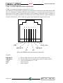
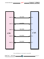
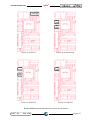
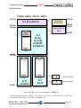
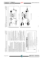
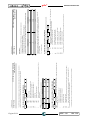
1
GPC® 324 General Purpose Controller 80C32, 80C320, etc. serie 4 MANUALE TECNICO Via dell' Artigiano, 8/6 ® 40016 San Giorgio di Piano grifo (Bologna) ITALY E-mail: [email protected] http://www.grifo.it http://www.grifo.com Tel. +39 051 892.052 (r.a.) FAX: +39 051 893.661 ITALIAN TECHNOLOGY GPC® 324 Edizione 3.20 Rel. 13 Luglio 2000 ® ® , GPC , grifo , sono marchi registrati della ditta grifo® GPC® 324 General Purpose Controller 80C32, 80C320, etc. serie 4 MANUALE TECNICO Modulo Intelligente Abaco® BLOCK, della serie 4, nel formato 100x50 mm. Contenitore, opzionale, per guide ad Ω tipo DIN 46277-1 e DIN 46277-3. CPU 80c32 o 80C320, da 22 MHz e tutti i modelli compatibili. E' inoltre completamente supportata la programmazione in system dei PHILIPS 89CRx+/2. Configurazione di memoria massima di 104K Bytes: 32K SRAM, zoccolo per 32K EPROM, zoccolo per 32K EPROM SRAM EPROM FLASH EPROM ed EEPROM seriale da 256 a 8192 Bytes. Real Time Clock autonomo in grado di generare INT. Circuiteria di Back Up per SRAM e RTC, tramite batteria al LITIO di bordo ed esterna. Watch dog settabile via hardware e software. 5 linee TTL di I/O; tre timer counter a 16 bits; jumper per selezione modo RUN/DEBUG. 2 linee seriali in RS232, di cui una settabile in RS422, RS485 o current loop. Connettore di espansione standard ABACO® I/O BUS da 26 vie. Numerose sorgenti d'interrupt, tra cui un'efficiente circuiteria di Power Failure. Unica tensione di alimlentazione a 5Vdc, 115 mA con diverse modalita' di riduzione consumi. Protezione della logica di bordo dai transienti tramite TransZorb™. Vasta disponibilità di software di sviluppo quali: Monitor Debugger (MDP, FMO52, NOICE); Assembler (MCA51); GET 51; compilatori C (MCC51, HTC51, SYS51CW, DDS Micro C51); BASIC (BASIC 324, BXC51, BASCOM 8051); compilatori PASCAL (SYS51PW); ecc. Via dell' Artigiano, 8/6 ® 40016 San Giorgio di Piano grifo (Bologna) ITALY E-mail: [email protected] http://www.grifo.it http://www.grifo.com Tel. +39 051 892.052 (r.a.) FAX: +39 051 893.661 ITALIAN TECHNOLOGY GPC® 324 Edizione 3.20 Rel. 13 Luglio 2000 ® ® , GPC , grifo , sono marchi registrati della ditta grifo® Vincoli sulla documentazione grifo® Tutti i Diritti Riservati Nessuna parte del presente manuale può essere riprodotta, trasmessa, trascritta, memorizzata in un archivio o tradotta in altre lingue, con qualunque forma o mezzo, sia esso elettronico, meccanico, magnetico ottico, chimico, manuale, senza il permesso scritto della grifo®. IMPORTANTE Tutte le informazioni contenute in questo manuale sono state accuratamente verificate, ciononostante grifo® non si assume nessuna responsabilità per danni diretti o indiretti a cose e/o persone derivanti da errori tecnici ed omissioni o dall'uso del presente manuale, del software o dell' hardware ad esso associato. grifo® altresi si riserva il diritto di modificare il contenuto e la veste di questo manuale senza alcun preavviso, con l' intento di offrire un prodotto sempre migliore, senza che questo rappresenti un obbligo per grifo®. Per le informazioni specifiche sui componenti montati sulla scheda, l'utente deve fare riferimento ai Data Book delle case costruttrici o delle seconde sorgenti. LEGENDA SIMBOLI Nel presente manuale possono comparire i seguenti simboli: Attenzione: Pericolo generico Attenzione: Pericolo di alta tensione Marchi Registrati , GPC®, grifo® : sono marchi registrati della grifo®. Altre marche o nomi di prodotti sono marchi registrati dei rispettivi proprietari. ITALIAN TECHNOLOGY grifo® INDICE GENERALE INTRODUZIONE......................................................................................................................... 1 VERSIONE SCHEDA .................................................................................................................. 1 CARATTERISTICHE GENERALI ........................................................................................... 2 ABACO® I/O BUS ...................................................................................................................... 3 COMUNICAZIONE SERIALE ............................................................................................... 3 PROCESSORE .......................................................................................................................... 4 CLOCK ...................................................................................................................................... 4 DISPOSITIVI PERIFERICI DI BORDO ............................................................................... 6 CONTATTO DI RESET............................................................................................................ 6 DISPOSITIVI DI MEMORIA ................................................................................................. 7 LOGICA DI CONTROLLO ..................................................................................................... 7 ALIMENTAZIONE ................................................................................................................... 7 SPECIFICHE TECNICHE ......................................................................................................... 8 CARATTERISTICHE GENERALI ........................................................................................ 8 CARATTERISTICHE FISICHE ............................................................................................. 8 CARATTERISTICHE ELETTRICHE ................................................................................... 9 INSTALLAZIONE ..................................................................................................................... 10 CONNESSIONI CON IL MONDO ESTERNO ................................................................... 10 CN2 - CONNETTORE PER BATTERIA ESTERNA DI BACK UP .............................. 10 CN1 - CONNETTORE PER ABACO® I/O BUS .............................................................. 11 CN3A - CONNETTORE PER LINEA SERIALE A ......................................................... 12 CN3B - CONNETTORE PER LINEA SERIALE B ......................................................... 14 CN5 - CONNETTORE PER I/O E TENSIONE DI PROG. DELLA CPU ..................... 20 INTERFACCIAMENTO DEGLI I/O CON IL CAMPO ..................................................... 22 INTERFACCE PER I/O DIGITALI ...................................................................................... 22 JUMPERS ................................................................................................................................ 24 JUMPERS A 2 VIE ............................................................................................................... 26 JUMPERS A 3 VIE ............................................................................................................... 27 JUMPERS A 5 VIE ............................................................................................................... 27 SELEZIONE MEMORIE ....................................................................................................... 28 JUMPER A STAGNO.............................................................................................................. 28 INTERRUPTS.......................................................................................................................... 29 RESET E WATCH DOG ........................................................................................................ 29 COMUNICAZIONE SERIALE ............................................................................................. 30 BACK UP ................................................................................................................................. 33 POWER FAILURE .................................................................................................................. 33 PROGRAMMAZIONE IN SYSTEM (ISP) .......................................................................... 33 DESCRIZIONE SOFTWARE ................................................................................................... 34 GPC® 324 Rel. 3.20 Pagina I grifo® ITALIAN TECHNOLOGY MAPPAGGI ED INDIRIZZAMENTI ...................................................................................... 36 INTRODUZIONE.................................................................................................................... 36 MAPPAGGIO DELLE RISORSE DI BORDO .................................................................... 36 MAPPAGGIO DELLE MEMORIE ...................................................................................... 36 MAPPAGGIO 0 .................................................................................................................... 37 MAPPAGGIO 1 .................................................................................................................... 38 MAPPAGGIO 3 .................................................................................................................... 39 MAPPAGGIO DELL’I/O ........................................................................................................ 40 DESCRIZIONE SOFTWARE DELLE PERIFERICHE DI BORDO .................................. 41 INGRESSO CONFIGURAZIONE: J1 (RUN/DEBUG) ...................................................... 41 WATCH DOG ESTERNO ...................................................................................................... 41 DIREZIONALITA' RS 422, RS 485 ...................................................................................... 41 EEPROM SERIALE ............................................................................................................... 42 REAL TIME CLOCK ............................................................................................................. 42 PERIFERICHE DELLA CPU ............................................................................................... 43 SCHEDE ESTERNE .................................................................................................................. 44 BIBLIOGRAFIA ........................................................................................................................ 48 APPENDICE A: MONTAGGIO MECCANICO ................................................................... A-1 APPENDICE B: DESCRIZIONE COMPONENTI DI BORDO ......................................... B-1 µP 80C32 ................................................................................................................................. B-1 µP 80C320 ............................................................................................................................... B-7 FAMIGLIA 51 ..................................................................................................................... B-14 APPENDICE C: SCHEMI ELETTRICI ............................................................................... C-1 APPENDICE D: INDICE ANALITICO ................................................................................ D-1 Pagina II GPC® 324 Rel. 3.20 ITALIAN TECHNOLOGY grifo® INDICE DELLE FIGURE FIGURA 1: CARATTERISTICHE MICROPROCESSORE ............................................................................. 4 FIGURA 2: SCHEMA A BLOCCHI ......................................................................................................... 5 FIGURA 3: FOTO DELLA SCHEDA ....................................................................................................... 9 FIGURA 4: CN2 - CONNETTORE PER BATTERIA ESTERNA DI BACK UP ............................................... 10 FIGURA 5: CN1 - CONNETTORE PER ABACO® I/O BUS .............................................................. 11 FIGURA 6: CN3A-CONNETTORE PER LINEA SERIALE A ................................................................... 12 FIGURA 7: DISPOSIZIONE P1, MEMORIE, BATTERIA E CONNETTORI ................................................... 13 FIGURA 8: CN3B-CONNETTORE PER LINEA SERIALE B ................................................................... 14 FIGURA 9: SCHEMA DI COMUNICAZIONE SERIALE ............................................................................. 15 FIGURA 10: ESEMPIO COLLEGAMENTO PUNTO PUNTO IN RS 232 ..................................................... 16 FIGURA 11: ESEMIPO COLLEGAMENTO PUNTO PUNTO IN RS 422 ..................................................... 16 FIGURA 12: ESEMPIO COLLEGAMENTO PUNTO PUNTO IN RS 485 ..................................................... 16 FIGURA 13: ESEMPIO COLLEGAMENTO IN RETE IN RS 485 .............................................................. 17 FIGURA 14: ESEMPIO COLLEGAMENTO PUNTO PUNTO IN CURRENT LOOP A 4 FILI .............................. 18 FIGURA 15: ESEMPIO COLLEGAMENTO PUNTO PUNTO IN CURRENT LOOP A 2 FILI .............................. 18 FIGURA 16: ESEMPIO COLLEGAMENTO RETE IN CURRENT LOOP A 4 FILI ........................................... 19 FIGURA 17: CN5 - CONNETTORE PER I/O E TENSIONE DI PROGRAMMAZIONE DELLA CPU ................ 20 FIGURA 18: SCHEMA COLLEGAMENTO LINEE DI I/O ........................................................................ 21 FIGURA 19: PIANTA COMPONENTI (LATO COMPONENTI) ................................................................... 23 FIGURA 20: PIANTA COMPONENTI (LATO STAGNATURE) .................................................................... 23 FIGURA 21: TABELLA RIASSUNTIVA JUMPERS ................................................................................... 24 FIGURA 22: DISPOSIZIONE JUMPERS LATO COMPONENTI ................................................................... 25 FIGURA 23: DISPOSIZIONE JUMPERS LATO STAGNATURE ................................................................... 25 FIGURA 24: TABELLA JUMPERS A 2 VIE ........................................................................................... 26 FIGURA 25: TABELLA JUMPERS A 3 VIE ........................................................................................... 27 FIGURA 26: TABELLA JUMPERS A 5 VIE ........................................................................................... 27 FIGURA 27: TABELLA DI SELEZIONE MEMORIE ................................................................................ 28 FIGURA 28: DISPOSIZIONE DRIVER PER COMUNICAZIONE SERIALE .................................................... 31 FIGURA 29: MAPPAGGIO DELLE MEMORIE IN MODO 0 .................................................................. 37 FIGURA 30: MAPPAGGIO DELLE MEMORIE IN MODO 1 .................................................................. 38 FIGURA 31: MAPPAGGIO DELLE MEMORIE IN MODO 3 .................................................................. 39 FIGURA 32: TABELLA INDIRIZZAMENTO I/O .................................................................................... 40 FIGURA 33: SCHEMA DELLE POSSIBILI CONNESSIONI PER GPC® 324 ............................................... 45 FIGURA A1: DIMA DI FORATURA PER MONTAGGIO IN PIGGY BACK ................................................. A-1 FIGURA A2: MONTAGGIO IN PIGGY-BACK .................................................................................... A-2 FIGURA A3: MONTAGGIO SU GUIDA WEIDMULLER ........................................................................ A-2 FIGURA C1: SCHEMA ELETTRICO DI ESPANSIONE PPI ................................................................... C-1 FIGURA C2: SCHEMA ELETTRICO SPA 03 .................................................................................... C-2 FIGURA C3: SCHEMA ELETTRICO QTP 16P ................................................................................. C-3 FIGURA C4: SCHEMA ELETTRICO QTP 24P 1/2 ........................................................................... C-4 FIGURA C5: SCHEMA ELETTRICO QTP 24P 2/2 ........................................................................... C-5 FIGURA C6: SCHEMA ELETTRICO IAC 01 .................................................................................... C-6 FIGURA C7: SCHEMA ELETTRICO DI I/O SU ABACO® I/O BUS .................................................. C-7 FIGURA C8: SCHEMA ELETTRICO INTERFACCIA BUS .................................................................... C-8 GPC® 324 Rel. 3.20 Pagina III grifo® Pagina IV ITALIAN TECHNOLOGY GPC® 324 Rel. 3.20 ITALIAN TECHNOLOGY grifo® INTRODUZIONE L’uso di questi dispositivi è rivolto - IN VIA ESCLUSIVA - a personale specializzato. Scopo di questo manuale è la trasmissione delle informazioni necessarie all’uso competente e sicuro dei prodotti. Esse sono il frutto di un’elaborazione continua e sistematica di dati e prove tecniche registrate e validate dal Costruttore, in attuazione alle procedure interne di sicurezza e qualità dell'informazione. I dati di seguito riportati sono destinati - IN VIA ESCLUSIVA - ad un utenza specializzata, in grado di interagire con i prodotti in condizioni di sicurezza per le persone, per la macchina e per l’ambiente, interpretando un’elementare diagnostica dei guasti e delle condizioni di funzionamento anomale e compiendo semplici operazioni di verifica funzionale, nel pieno rispetto delle norme di sicurezza e salute vigenti. Le informazioni riguardanti installazione, montaggio, smontaggio, manutenzione, aggiustaggio, riparazione ed installazione di eventuali accessori, dispositivi ed attrezzature, sono destinate - e quindi eseguibili - sempre ed in via esclusiva da personale specializzato avvertito ed istruito, o direttamente dall’ASSISTENZA TECNICA AUTORIZZATA, nel pieno rispetto delle raccomandazioni trasmesse dal costruttore e delle norme di sicurezza e salute vigenti. I dispositivi non possono essere utilizzati all'aperto. Si deve sempre provvedere ad inserire i moduli all'interno di un contenitore a norme di sicurezza che rispetti le vigenti normative. La protezione di questo contenitore non si deve limitare ai soli agenti atmosferici, bensì anche a quelli meccanici, elettrici, magnetici, ecc. Per un corretto rapporto coi prodotti, è necessario garantire leggibilità e conservazione del manuale, anche per futuri riferimenti. In caso di deterioramento o più semplicemente per ragioni di approfondimento tecnico ed operativo, consultare direttamente l’Assistenza Tecnica autorizzata. Al fine di non incontrare problemi nell’uso di tali dispositivi, è conveniente che l’utente - PRIMA DI COMINCIARE AD OPERARE - legga con attenzione tutte le informazioni contenute in questo manuale. In una seconda fase, per rintracciare più facilmente le informazioni necessarie, si può fare riferimento all’indice generale e all’indice analitico, posti rispettivamente all’inizio ed alla fine del manuale. VERSIONE SCHEDA Il presente manuale è riferito alla scheda GPC® 324 versione 110400 e sucessive. La validità delle informazioni riportate è quindi subordinata al numero di versione della scheda in uso e l'utente deve quindi sempre verificare la giusta corrispondenza tra le due indicazioni. Sulla scheda il numero di versione è riportato in più punti sia a livello di serigrafia che di stampato (ad esempio vicino al connettore CN5 ed allo zoccolo IC14 sul lato componenti). GPC® 324 Rel. 3.20 Pagina 1 grifo® ITALIAN TECHNOLOGY CARATTERISTICHE GENERALI La scheda GPC® 324, che fa parte della Serie 4 delle CPUcon ingombro di 100x50 mm, é un potente modulo di controllo, della fascia a basso prezzo, in grado di funzionare autonomamente come periferica intelligente e/o remotata in una più vasta rete di telecontrollo e/o di acquisizione. La GPC® 324 può essere fornita di un supporto in plastica provvisto degli attacchi per le guide ad Omega tipo DIN 46277-1 e DIN 46277-3. In questo modo non é necessario l’uso di un rack, ma la scheda può essere montata, in modo più economico, direttamente nel quadro elettrico. Viste le ridotte dimensioni della scheda GPC® 324, questa può essere montata nella stessa guida in plastica che contiene le periferiche di I/O, come ad esempio le ZBR xxx e ZBT xxx , formando in questo modo un unico elemento BLOCK. Un'altra tipica applicazione della scheda GPC® 324, é quella di essere adoperata come un modulo di CPU da montare in Piggy Back su schede periferiche realizzate direttamente dall'utente; in questo caso e' possibile realizzare una rapida prototipizzazione tramite schede come la SPA 03 e SPA 04. La presenza dell'ABACO® I/O BUS consente inoltre di poter pilotare direttamente le schede CAN 14, ADC 812, DAC 212, ecc. ed anche le numerose schede periferiche disponibili sul BUS ABACO®, tramite l'ABB 03, ABB 05. L'aspetto più interessante di questa scheda é data dal fatto che può essere equipaggiata da una vasta schiera di µP. E' infatti possibile averla con il normale 80C32; con il velocissimo DALLAS 80C320, con i nuovi PHILIPS 89CRx+/2o con molti dei modelli compatibili. Le caratteristiche della scheda rimangono fondamentalmente le stesse pur variando notevolmente in prestazioni a secondo del tipo di µP montato. Attualmente sono disponibili diversi pacchetti software che consentono di usare la scheda come sistema di sviluppo di se stessa, sia in assembler che con linguaggi evoluti. Una particolare menzione va' ai vari compilatori C, PASCAL e BASIC ed il comodo BASIC 324. Quest'ultimo é compatibile con il diffusissimo MCS® BASIC 52 della INTEL, a cui sono stati aggiunti dei nuovi comandi. Tra i nuovi é doveroso citarne alcuni come quelli relativi alla seconda linea seriale ed all'EEPROM seriale. Aggiungendo un 82C55, esterno alla scheda é possibile gestire dei display LCD o Fluorescenti e di una tastiera a matrice. Per un uso immediato di questi nuovi comandi, sono disponibili delle schede della serie KDx x24 oppure, per chi ha bisogno di un oggetto finito, esiste il pannello operatore tipo QTP xxP. Questi pannello operatore, offerto nella versione a giorno, ha la stessa estetica della QTP xx ma, non disponendo di intelligenza locale viene comandato direttamente dalla GPC® 324, consentendo così una notevole riduzione dei costi. Il BASIC 324 e l'accoppiata BASCOM 8051 + FMO52, oltre alla nota facilità di debugger, consente di programmare direttamente a bordo scheda una EEPROM o FLASH EPROM con il programma utente. - Modulo Intelligente Abaco® BLOCK, della serie 4, nel formato 100x50 mm. - Contenitore, opzionale, per guide ad Ω tipo DIN 46277-1 e DIN 46277-3. - CPU 80c32 o 80C320, da 22 MHz e tutti i modelli compatibili. E' inoltre completamente supportata la programmazione in system dei PHILIPS 89CRx+/2. - Configurazione di memoria massima di 104K Bytes: 32K SRAM, zoccolo per 32K EPROM, zoccolo per 32K EPROM SRAM EPROM FLASH EPROM ed EEPROM seriale da 256 a 8192 Bytes. - Real Time Clock autonomo in grado di generare INT. - Circuiteria di Back Up per SRAM e RTC, tramite batteria al LITIO di bordo ed esterna. - Watch dog settabile via hardware e software. - 5 linee TTL di I/O; tre timer counter a 16 bits; jumper per selezione modo RUN/ DEBUG. - 2 linee seriali in RS232, di cui una settabile in RS422, RS485 o current loop. Pagina 2 GPC® 324 Rel. 3.20 ITALIAN TECHNOLOGY grifo® - Connettore di espansione standard ABACO® I/O BUS da 26 vie. - Numerose sorgenti d'interrupt, tra cui un'efficiente circuiteria di Power Failure. - Unica tensione di alimlentazione a 5Vdc, 115 mA con diverse modalita' di riduzione consumi. - Protezione della logica di bordo dai transienti tramite TransZorb™. - Vasta disponibilità di software di sviluppo quali: Monitor Debugger (MDP, FMO52, NOICE); Assembler (MCA51); GET 51; compilatori C (MCC51, HTC51, SYS51CW, DDS Micro C51); BASIC (BASIC 324, BXC51, BASCOM 8051); compilatori PASCAL (SYS51PW); ecc. Viene di seguito riportata una descrizione dei blocchi funzionali della scheda, con indicate le operazioni effettuate da ciascuno di essi. Per una più facile individuazione di tali blocchi e per una verifica delle loro connessioni, fare riferimento alla figura 1. ABACO® I/O BUS Una delle caratteristiche di fondamentale importanza della GPC® 324 è quella di disporre del cosiddetto ABACO® I/O BUS, ovvero un connettore normalizzato con cui è possibile collegare la scheda ad una serie di moduli esterni intelligenti e non. Tra questi si trovano moduli per l'acquisizione di segnali analogici (A/D), per la generazione di segnali analogici (D/A), per la gestione di linee di I/O logico, per counter, ecc. e ne possono essere realizzati anche su specifiche richieste dell'utente. Utilizzando un mother board come l'ABB 03 o l'ABB 05 é inoltre possibile gestire tutte le schede periferiche in formato europa con interfaccia per BUS ABACO®. Tale caratteristica rende la scheda espandibile con un ottimo rapporto prezzo/prestazioni e quindi adatta a risolvere molti dei problemi dell'automazione industriale. COMUNICAZIONE SERIALE La GPC® 324 dispone sempre di una linea seriale hardware (definita seriale A) ed una seconda linea seriale (definita seriale B) gestita come segue: µP 80C32: µP 80C320: seriale software gestita tramite due linee di I/O del microprocessore; seriale hardware gestita tramite registri interni del microprocessore; Il protocollo fisico (baud rate, stop bit, bit x chr, ecc.) delle linee seriali hardware é completamente settabile via software tramite la programmazione dei registri interni al microcontrollore di cui la scheda è provvista, quindi per ulteriori informazioni si faccia riferimento alla documentazione tecnica della casa costruttrice o alle appendici di questo manuale. Per la linea seriale software il protocollo fisico é invece direttamente definito da apposite procedure che agiscono direttamente sulla linea di ricezione e trasmissione. Alcuni pacchetti software (come il BASIC 324 ed il BASCOM 8051) gestiscono la linea seriale software tramite istruzioni ad alto livello. La linea seriale B è sempre bufferata in RS 232 mentre per la seriale A è possibile selezionare, tramite una serie di comodi jumpers, il protocollo elettrico di comunicazione. In particolare può essere bufferata in RS 232, Current Loop passivo, RS 422 o RS 485; in questi ultimi casi è definibile se la comunicazione avviene in full duplex o half duplex. GPC® 324 Rel. 3.20 Pagina 3 grifo® ITALIAN TECHNOLOGY PROCESSORE La scheda GPC® 324 è predisposta per accettare tutti i processori con pin out compatibile con la famiglia 51 INTEL, tra questi ricordiamo: 80C32, 80C52, 87C52, 89C52 (prodotti da INTEL e numerose altre case), 89S8252 (prodotto da ATMEL), 89CRx+/2 (prodotti da PHILIPS), 80C320,87C320 (prodotti da DALLAS). Tali processori ad 8 bits sono codice compatibile con la famiglia INTEL 8051, largamente diffusa a livello mondiale, e sono caratterizzati da: un esteso set di istruzioni, un’alta velocità di esecuzone e di manipolazione dati, da un efficiente gestione degli interrupts e da una ricca serie di periferiche harware integrate. In questo manuale in tutti i paragrafi viene riportata una descrizione delle caratteristiche comuni a tutti i microprocessori effettuando, quando necessario, le dovute distinzioni. Di seguito viene riportato un elenco delle caratteristiche principali delle CPU disponibili: Microprocessore Dimensione BUS dati Clock per ciclo macchina RAM interna (bytes) ROM interna (kbytes) EEPROM interna (kbytes) Area codice esterna (kbytes) Area dati esterna (kbytes) Ports di I/O Timer/Counters a 16 bits Sorgenti d'nterrupt Livelli di priorità interrupt Linee seriali a/sincrone Modalità a basso consumo Gestione consumo e controllo Watch dog timer interno Programmazione su scheda Programmazione da applicativo 80C32 8 12 256 8 0 64 64 4 3 6 2 1 Si No No No No 89S8252 89CRx+/2 80C320 8 8 8 12 6 4 256 256 256 8 64 8 2 0 0 64 64 64 64 64 64 4 4 4 3 3 3 9 7 13 2 4 3 1 1 2 Si Si Si Si No Si Si No Si Si Si No No Si No FIGURA 1: CARATTERISTICHE MICROPROCESSORE Per maggiori informazioni si faccia riferimento all’apposita documentazione della casa costruttrice o all'appendice B di questo manuale. Si ricorda che la precedente tabella descrive le caratteristiche generali dei microprocessori ed alcune di queste possono non essere supportate dalla scheda. L'utente deve specificare il microprocessore richiesto durante la fase di ordine ed in caso di assenza di indicazioni la scheda é fornita nella sua versione base con 80C32. La versione con il DALLAS 80C320 é invece indicata con il suffisso D = GPC® 324D. CLOCK Sulla GPC® 324 é presente una circuiteria che provvede a generare la frequenza di clock per la CPU (22,1184 MHz); da cui vengono ricavate anche le frequenze necessarie per le altre sezioni della scheda (Timer Counter, Seriali, ecc.). Si ricorda inoltre che la frequenza di clock della CPU può essere divisa via software, in modo da ridurre il consumo. Pagina 4 GPC® 324 Rel. 3.20 grifo® ITALIAN TECHNOLOGY CN3A CN3B SERIAL LINE A SERIAL LINE B CN2 - BACK UP 3V LITHIUM BATTERY DRIVERS RS 232 RS 422 RS 485 CURRENT LOOP + RS 232 RTC IC7 SRAM IC 8 EPROM CPU 51 family IC 5 EPROM, SRAM, FLASH, EEPROM WATCH DOG POWER FAILURE IC 9 SERIAL EEPROM CN5 CN1 I/O lines, Vpp ABACO® I/O BUS JUMPER RUN/DEBUG CONTROL LOGIC FIGURA 2: SCHEMA A BLOCCHI GPC® 324 Rel. 3.20 Pagina 5 grifo® ITALIAN TECHNOLOGY DISPOSITIVI PERIFERICI DI BORDO La scheda GPC® 324, nata per risolvere molteplici problemi di controllo e comando di automatismi, è dotata di alcuni componenti periferici che si occupano dell’interfacciamento con il mondo esterno. In particolare: -Watch dog esterno: circuiteria di tipo astabile in grado di resettare la scheda ad intervallo di tempo di circa 1,4 sec. Via software l'utente é in grado di retriggerare la circuiteria per evitare il reset tramite l'acceso ad opportuni registri situati nello spazio d’indirizzamento della CPU. Nel caso in cui la scheda utilizzi microprocessori provvisti di sezione di watch dog interna l'utente può disporre di due circuiterie separate con caratteristiche diverse e quindi con un livello di sicurezza superiore. e conferisce al sistema basato sulla scheda, una sicurezza estrema - EEPROM seriale: il modulo di EEPROM seriale (IC9) è molto utile in caso si debbano mantenere delle informazioni anche in assenza di alimentazione, senza ricorrere al back up della RAM, con una sicurezza estrema sulla validità dei dati. Tale modulo può avere un size che varia nel range 256÷8192 bytes e di default viene montato un modulo con un size di 512 bytes. - Ingresso configurazione: sulla scheda é disponibile il jumper J1 per rendere configurabile la scheda ed in particolare il programma applicativo sviluppato. La possibilità di acquisire via software lo stato di questo jumper, fornisce all’utente la possibilità di gestire diverse condizioni tramite un unico programma, senza dover rinunciare ad altre linee d’ingresso (le applicazioni caratteristiche sono: selezione della lingua di rappresentazione, definizione parametri del programma, selezione della modalità operativa, ecc.). Alcuni pacchettisoftware sviluppati per la GPC® 324 usano il jumper J1 per selezionare la modalità operativa di RUN o DEBUG, come descritto negli appositi manuali d'uso degli stessi pacchetti. - Real time clock: la GPC® 324 dispone di un completo Real Time Clock in grado di gestire ore, minuti, secondi, giorno del mese, mese, anno e giorno della settimana in modo completamente autonomo. L’alimentazione del componente é fornita dalla circuiteria di back up in modo da garantire la validità dei dati in ogni condizione operativa ed é completamente gestito via software, tramite la programmazione di 16 registri situati nello spazio di indirizzamento della CPU dalla logica di controllo. La sezione di RTC può inoltre generare interrupt in corrispondenza di intervalli di tempo programmabili via software, in modo da poter periodicamente distogliere la CPU dalle normali operazioni oppure periodicamente risvegliarla dagli stati di basso assorbimento. - Linee di I/O: cinque linee dei 4 port della CPU sono connesse al connettore CN5. La direzione delle linee é settabile a livello di bit e possono essere generati interrupt. In questo modo uno stato esterno può ottenere il controllo della CPU in ogni condizione con un minimo tempo di risposta. I port sono completamente gestiti via software tramite la programmazione degli appositi registri interni del microprocessore. Per ulteriori informazioni a riguardo dei dispositivi periferici descritti, si faccia riferimento al capitolo DESCRIZIONE SOFTWARE DELLE PERIFERICHE DI BORDO ed all'appendice B. CONTATTO DI RESET Sulla GPC® 324 è presente un contatto di reset (P1) che ha la funzione di resettare e quindi far ripartire la scheda da una condizione di azzeramento generale. La funzione principale di questo contatto è quella di uscire da condizioni di loop infinito, soprattutto durante la fase di debug o di garantire uno stato certo di partenza. Per una facile individuazione di tale contatto di reset a bordo scheda, si faccia riferimento alla figura 7. Pagina 6 GPC® 324 Rel. 3.20 ITALIAN TECHNOLOGY grifo® DISPOSITIVI DI MEMORIA E’ possibile dotare la scheda di un massimo di 104K di memoria variamente suddivisi con un massimo di 32K EPROM su zoccolo; 32K SRAM; 32K SRAM, EPROM, EEPROM o FLASH EPROM on socket ed infine 8K di EEPROM seriale. La scelta della configurazione delle memorie presenti sulla scheda può avvenire in relazione all'applicazione da risolvere e quindi in relazione alle esigenze dell'utente. Da questo punto di vista si ricorda che la scheda viene normalmente fornita con 32K SRAM di lavoro e 512 bytes di EEPROM seriale; tutte le rimanenti memorie devono essere quindi opportunamente specificate in fase di ordine della scheda. Tramite la circuiteria di back up presente a bordo scheda c'è inoltre la possibilità di tamponare i 32K RAM di lavoro (IC7) aggiungendo quindi la possibilità di mantenere i dati anche in assenza di alimentazione. Questa caratteristica fornisce alla scheda la possibilità di ricordare in ogni condizione, una serie di parametri come ad esempio la configurazione o lo stato del sistema. La circuiteria di back up è basata su due batterie: una a bordo scheda ed una esterna collegabile tramite un apposito connettore. Qualora la quantità di SRAM tamponata risulti insufficiente (ad esempio per sistemi di data loghin) si possono sempre utilizzare i moduli di RAM tamponata e/o di EEPROM su IC5. Il mappaggio delle risorse di memoria avviene tramite una opportuna circuiteria di bordo, che provvede ad allocare i dispositivi all’interno dello spazio d’indirizzamento del microprocessore; tale logica di controllo provvede a gestire in modo completamente automatico diversi tipi di mappaggi che si adattano ai diversi pacchetti software disponibili per la GPC® 324. Per maggiori informazioni fare riferimento ai paragrafi MAPPAGGIO DELLE MEMORIE e SELEZIONE MEMORIE. LOGICA DI CONTROLLO Il mappaggio di tutti i registri delle periferiche presenti sulla scheda e dei dispositivi di memoria, è affidata ad un’opportuna logica di controllo, realizzata con una logica programmabile, che si occupa di allocare tali dispositivi nello spazio d’indirizzamento della CPU. Per maggiori informazioni fare riferimento al capitolo MAPPAGGI ED INDIRIZZAMENTI. ALIMENTAZIONE L'unica tensione di alimentazione necessaria deve essere fornita tramite i pin 25 (GND) e 26 (+5 Vdc) del connettore CN1. Sulla scheda sono state adottate tutte le scelte circuitali e componentistiche che tendono a ridurre i consumi, compresa la possibilità di far lavorare alcuni microcontrollori in power down ed idle mode ed a ridurre la sensibilità ai disturbi. Una interessante circuiteria di power failure consente di riconoscere l'imminente caduta dell'alimentazione e quindi di intervenire opportunamente via software, tramite una procedura di risposta all'interrupt. Si ricorda inoltre che é presente una circuiteria di protezione tramite TransZorb™ per evitare danni dovuti a tensioni non corrette. GPC® 324 Rel. 3.20 Pagina 7 grifo® ITALIAN TECHNOLOGY SPECIFICHE TECNICHE CARATTERISTICHE GENERALI Risorse di bordo: 5 input/output programmabili TTL 1 linea bidirezionale RS 232, RS 422, RS 485 o Current Loop 1 linea bidirezionale RS 232 (hardware/software) 1 watch dog 1 contatto locale di reset 1 ingresso configurazione leggibile da software 1 interfaccia di espansione ABACO® I/O BUS 1 orologio tamponato 1 circuiteria di power failure Memoria indirizzabile: IC 8: IC 7: IC 5: IC 9: Tempo accesso memorie: 70 nsec CPU di bordo: INTEL 80C32 e compatibili ATMEL 89S8252 e compatibili PHILIPS 89CRx+/2 e compatibili DALLAS 80C320 e compatibili Frequenza di clock: 22,1184 MHz Tempo intervento watch dog: da 940 msec a 2060 msec (tipico 1420 msec) EPROM da 32K x 8 SRAM da 32K x 8 SRAM,EPROM,EEPROM,FLASH EPROM da 32K x 8 EEPROM seriale da 256 bytes a 8192 bytes CARATTERISTICHE FISICHE Dimensioni: 100 x 50 x 25 mm 110 x 60 x 60 mm (senza contenitore) (con contenitore per guide DIN) Peso: 75 g 130 g (senza contenitore) (con contenitore per guide DIN) Connettori: CN1: CN2: CN3A: CN3B: CN5: Range di temperatura: da 0 a 50 gradi Centigradi Umidità relativa: 20% fino a 90% Pagina 8 26 vie scatolino verticale M 2 vie scatolino verticale M PLUG a 6 vie PLUG a 6 vie 4+4 strip verticale M (senza condensa) GPC® 324 Rel. 3.20 grifo® ITALIAN TECHNOLOGY CARATTERISTICHE ELETTRICHE Tensione di alimentazione: +5 Vdc Corrente assorbita sui 5 Vdc: 115 mA 160 mA Batteria di back up di bordo: 3,0 Vdc; 180 mAh Batteria di back up esterna: 3,6÷5 Vdc Corrente di Back up: 4,2 µA 5,5 µA Rete terminazione RS422-485: terminazione linea = 120 Ω pull up sul positivo = 3,3 KΩ pull down sul negativo = 3,3 KΩ (configurazione default) (configurazione massima) (batteria di bordo) (batteria esterna da 3,6 V) Soglia intervento power failure: 52 mV prima dell'intervento del reset FIGURA 3: FOTO DELLA SCHEDA GPC® 324 Rel. 3.20 Pagina 9 grifo® ITALIAN TECHNOLOGY INSTALLAZIONE In questo capitolo saranno illustrate tutte le operazioni da effettuare per il corretto utilizzo della scheda. A questo scopo viene riportata l’ubicazione e la funzione dei connettori, dei jumpers ed alcuni diagrammi illustrativi. CONNESSIONI CON IL MONDO ESTERNO Il modulo GPC®324 è provvisto di 5 connettori con cui vengono effettuate tutte le connessioni con il campo e con le altre schede del sistema di controllo da realizzare. Di seguito viene riportato il loro pin out ed il significato dei segnali collegati; per una facile individuazione di tali connettori, si faccia riferimento alla figura 7, mentre per ulteriori informazioni a riguardo del tipo di connessioni, fare riferimento alle figure successive che illustrano il tipo di collegamento effettuato a bordo scheda. CN2 - CONNETTORE PER BATTERIA ESTERNA DI BACK UP CN2 è un connettore a scatolino, verticale, maschio, con passo 2,54 mm, a 2 vie. Tramite CN2 può essere collegata una batteria esterna che provveda a mantenere i dati della SRAM di bordo (IC7) e del real time clock anche in assenza di tensione di alimentazione. Per ulteriori informazioni vedere i paragrafi CARATTERISTICHE ELETTRICHE, BACK UP e SELEZIONE MEMORIE. +Vbat 1 2 GND FIGURA 4: CN2 - CONNETTORE PER BATTERIA ESTERNA DI BACK UP Legenda +Vbat GND Pagina 10 = I - Positivo della batteria esterna di back up = - Negativo della batteria esterna di back up GPC® 324 Rel. 3.20 grifo® ITALIAN TECHNOLOGY CN1 - CONNETTORE PER ABACO® I/O BUS CN1 è un connettore a scatolino, verticale, maschio, con passo 2.54 mm, a 26 piedini. Tramite CN1 si effettua la connessione tra la scheda e la serie di moduli esterni di espansione, da utilizzare per l’interfacciamento diretto con i segnali del campo. Tale collegamento è effettuato tramite lo standard ABACO® I/O BUS di cui questo connettore riporta tutti i segnali a livello TTL. D0 1 2 D1 D2 3 4 D3 D4 5 6 D5 D6 7 8 D7 A0 9 10 A1 A2 11 12 A3 A4 13 14 A5 A6 15 16 A7 /WR 17 18 /RD /IORQ 19 20 /RESET N.C. 21 22 N.C. /INT BUS 23 24 /NMI BUS GND 25 26 +5 Vdc FIGURA 5: CN1 - CONNETTORE PER ABACO® I/O BUS Legenda: A0-A7 = O D0-D7 = I/O /INT BUS = I /NMI BUS = I /IORQ = O /RD = O /WR = O /RESET = O +5 Vdc = I GND = N.C. = GPC® 324 Address BUS: BUS degli indirizzi. Data BUS: BUS dei dati. Interrupt request: richiesta d’interrupt. Deve essere in open collector Non Mascable Interrupt: richiesta d’interrupt non mascherabile. Input Output Request: richiesta operazione Input Output su I/O BUS. Read cycle status: richiesta di lettura. Write cycle status: richiesta di scrittura. Reset: azzeramento. Linea di alimentazione a +5 Vdc. Linea di massa. Non Collegato. Rel. 3.20 Pagina 11 grifo® ITALIAN TECHNOLOGY CN3A - CONNETTORE PER LINEA SERIALE A CN3A è un connettore femmina, del tipo PLUG a 6 vie. Sul connettore sono disponibili i segfnali per la comunicazione della linea seriale A, in RS 232, RS 422, RS 485 o Current Loop,che é fisicamente collegato alla linea seriale hardware 0 dem microprocessore. La disposizione di tali segnali, riportata di seguito, è stata studiata in modo da ridurre al minimo le interferenze ed in modo da facilitare la connessione con il campo, mentre i segnali rispettano le normative definite dal CCITT relative ad ognuno degli standard di comunicazione usati. 6 5 4 3 2 1 GND +5 Vdc / GND RXA RS232 / RXA+ RS422 / RXTXA+ RS485 / RXA+ C.L. RXA- RS422 / RXTXA- RS485 / RXA- C.L. TXA RS232 / TXA+ RS422 / TXA- C.L. TXA- RS422 / TXA+ C.L. FIGURA 6: CN3A-CONNETTORE PER LINEA SERIALE A Legenda: RXA RS232 TXA RS232 RXA- RS422 RXA+ RS422 TXA- RS422 TXA+ RS422 RXTXA- RS485 Pagina 12 = I - Receive Data: linea ricezione in RS 232 della seriale A. = O - Transmit Data: linea trasmissione in RS 232 della seriale A. = I - Receive Data Negative: linea bipolare negativa di ricezione differenziale in RS 422 della seriale A. = I - Receive Data Positive: linea bipolare positiva di ricezione differenziale in RS 422 della seriale A. = O - Transmit Data Negative: linea bipolare negativa di trasmissione differenziale in RS 422 della seriale A. = O - Transmit Data Positive: linea bipolare positiva di trasmissione differenziale in RS 422 della seriale A. =I/O- Receive Transmit Data Negative: linea bipolare negativa di ricezione e trasmissione differenziale in RS 485 della seriale A. GPC® 324 Rel. 3.20 grifo® ITALIAN TECHNOLOGY RXTXA+ RS485 RXA- C.L. RXA+ C.L. TXA- C.L. TXA+ C.L. +5 Vdc GND =I/0- Receive Transmit Data Positive: linea bipolare positiva di ricezione e trasmissione differenziale in RS 485 della seriale A. = I - Receive Data Negative: linea bipolare negativa di ricezione in Current Loop della seriale A. = I - Receive Data Positive: linea bipolare positiva di ricezione in Current Loop della seriale A. = O - Transmit Data Negative: linea bipolare negativa di trasmissione in Current Loop della seriale A. = O - Transmit Data Positive: linea bipolare positiva di trasmissione in Current Loop della seriale A. = I - Linea di alimentazione a +5 Vdc. = - Linea di massa. CN3A CN3B BT1 CN5 IC8 CN1 EPROM IC5 CN2 SRAM,FLASH EEPROM, EPROM P1 FIGURA 7: DISPOSIZIONE P1, MEMORIE, BATTERIA E CONNETTORI GPC® 324 Rel. 3.20 Pagina 13 grifo® ITALIAN TECHNOLOGY CN3B - CONNETTORE PER LINEA SERIALE B CN3B è un connettore femmina, del tipo PLUG a 6 vie. Sul connettore sono disponibili i segfnali per la comunicazione della linea seriale B bufferata in RS 232 che é fisicamente collegato alla linea seriale hardware 1 o software del microprocessore. La disposizione di tali segnali, riportata di seguito, è stata studiata in modo da ridurre al minimo le interferenze ed in modo da facilitare la connessione con il campo, mentre i segnali rispettano le normative definite dal CCITT relative ad ognuno degli standard di comunicazione usati. 6 5 4 3 2 GND 1 +5 Vdc / GND RXB RS232 TXB RS232 N.C. N.C. FIGURA 8: CN3B-CONNETTORE PER LINEA SERIALE B Legenda: RXB RS232 TXB RS232 +5 Vdc GND N.C. Pagina 14 = I - Receive Data: linea di ricezione in RS 232 della seriale B. = O - Transmit Data: linea di trasmissione in RS 232 della seriale B. = I - Linea di alimentazione a +5 Vdc. = - Linea di massa. = - Non Collegato. GPC® 324 Rel. 3.20 grifo® ITALIAN TECHNOLOGY DIR RS 422 RS 485 CURRENT LOOP DRIVERS C P U HARDWARE SERIAL LINE A C N 3 A RS 232 D R I V E R SOFTWARE/ HARDWARE SERIAL LINE B C N 3 B FIGURA 9: SCHEMA DI COMUNICAZIONE SERIALE GPC® 324 Rel. 3.20 Pagina 15 ITALIAN TECHNOLOGY 5 RXA, RXB TX 2 TXA, TXB RX 6 GND GND External System CN3A,B GPC® 324 grifo® FIGURA 10: ESEMPIO COLLEGAMENTO PUNTO PUNTO IN RS 232 RXA - TX- RXA+ TX+ TXA- RX- TXA+ RX+ GND GND 5 3 External System CN3A GPC® 324 4 2 6 RXTXA- TX- / RX- RXTXA+ TX+ / RX+ 4 5 GND GND External System CN3A GPC® 324 FIGURA 11: ESEMIPO COLLEGAMENTO PUNTO PUNTO IN RS 422 6 FIGURA 12: ESEMPIO COLLEGAMENTO PUNTO PUNTO IN RS 485 Pagina 16 GPC® 324 Rel. 3.20 grifo® ITALIAN TECHNOLOGY Master + Tx / Rx - + 120 Ω 4 6 TXRXA CN3A GND GPC® 324 Unit GND Slave 1 5 Slave 2 6 + TXRXA GND +5V 5 + 4 GPC® 324 Unit 4 CN3A Slave n CN3A TXRXA - 6 GND GPC® 324 Unit 5 FIGURA 13: ESEMPIO COLLEGAMENTO IN RETE IN RS 485 Da notare che in una rete RS 485, devono essere presenti due resistenze di forzatura lungo la linea e due resitenze di terminazione (120 Ω), alle estremità della stessa, rispettivamente vicino all'unità Master ed all'ultima unità Slave. A bordo della GPC® 324 è presente la circuiteria di terminazione e forzatura, che può essere inserita o disinserita, tramite appositi jumpers, come illutrato in seguito. In merito alla resistenza di terminazione dell'unità Master, provvedere a collegarla solo se questa non é già presente al suo interno (ad esempio molti convertitori RS232-RS485 ne sono già provvisti). Per maggiori informazioni consultare il Data-Book TEXAS INSTRUMENTS, "RS 422 and RS 485 Interface Cicuits", nella parte introduttiva riguardante le reti RS 422-485. GPC® 324 Rel. 3.20 Pagina 17 grifo® - VCL ITALIAN TECHNOLOGY + R RXA - Master Remote System TX+ CN3A GPC® 324 4 RXA+ TX- 5 R TXA - RX+ 2 RX- TXA+ 3 FIGURA 14: ESEMPIO COLLEGAMENTO PUNTO PUNTO IN CURRENT LOOP A 4 FILI - VCL + R RXA - TX+ RXA+ TX- TXA- RX+ TXA+ RX- External System CN3A GPC® 324 4 5 2 3 FIGURA 15: ESEMPIO COLLEGAMENTO PUNTO PUNTO IN CURRENT LOOP A 2 FILI Pagina 18 GPC® 324 Rel. 3.20 grifo® ITALIAN TECHNOLOGY + Master R Slave 1 5 + RXA 4 - + TX R + RX - VCL CN3A + TXA 2 GPC® 324 Unit 3 Slave 2 5 + RXA 4 CN3A 3 + TXA 2 GPC® 324 Unit Slave n 5 + RXA 4 CN3A 3 + TXA 2 GPC® 324 Unit FIGURA 16: ESEMPIO COLLEGAMENTO RETE IN CURRENT LOOP A 4 FILI Per il collegamento in Current Loop passivo sono possibili due diversi tipi di collegamento: a 2 fili ed a 4 fili. Tali connessioni sono riportate nelle figure 14÷16; in esse é indicata la tensione per alimentare l’anello (VCL) e le resistenze di limitazione della corrente (R). I valori di tali componenti variano in funzione del numero di dispositivi collegati e della caduta sul cavo di collegamento; bisogna quindi effettuare la scelta considerando che: - si deve garantire la circolazione di una corrente di 20 mA; - su ogni trasmettitore cadono mediamente 2,35 V con una corrente di 20 mA; - su ogni ricevitore cadono mediamente 2,52 V con una corrente di 20 mA; - in caso di cortocircuito sulla rete ogni trasmettitore dissipi al massimo 125 mW; - in caso di cortocircuito sulla rete ogni ricevitore dissipi al massimo 90 mW. Per maggiori informazioni consultare il manuale HEWLETT-PACKARD, nella parte che riguarda gli opto accoppiatori per Current Loop denominati HCPL 4100 e HCPL 4200. GPC® 324 Rel. 3.20 Pagina 19 grifo® ITALIAN TECHNOLOGY CN5 - CONNETTORE PER I/O E TENSIONE DI PROGRAMMAZIONE DELLA CPU CN5 è un connettore a strip, verticale, con passo 2.54 mm, a 4+4 piedini. Tramite CN5 si effettua la connessione tra alcuni segnali dei port 1 e 3 della CPU e l’ambiente esterno e l'eventuale tensione di programmazione richiesta dalla programmazione in system dei microcontrollori PHILIPS. Da ricordare che la linea P3.3 può essere usata solo quando il jumper J2 é non connesso. P1.5 1 2 P1.4 P1.6 3 4 P1.7 GND 5 6 +5 Vdc P3.3 7 8 Vpp FIGURA 17: CN5 - CONNETTORE PER I/O E TENSIONE DI PROGRAMMAZIONE DELLA CPU Legenda: P1.n P3.3 Vpp +5 Vdc GND Pagina 20 = I/O - Linea digitale n del port 1 della CPU. = I/O - Linea digitale 3 del port 3 della CPU = /INT1. = I - Tensione di programmazione a +12 Vdc o +5 Vdc (per ulteriori informazioni vedere paragrafo PROGRAMMAZIONE IN SYSTEM) = O - Linea di alimentazione a +5 Vdc. = - Linea di massa per sezione digitale. GPC® 324 Rel. 3.20 grifo® ITALIAN TECHNOLOGY I/O LINE PORT 1.4 I/O LINE PORT 1.5 I/O LINE PORT 1.6 PIN 2 PIN 1 PIN 3 CN5 CPU I/O LINE PORT 1.7 I/O LINE PORT 3.3 PIN 4 PIN 7 FIGURA 18: SCHEMA COLLEGAMENTO LINEE DI I/O GPC® 324 Rel. 3.20 Pagina 21 grifo® ITALIAN TECHNOLOGY INTERFACCIAMENTO DEGLI I/O CON IL CAMPO Al fine di evitare eventuali problemi di collegamento della scheda con tutta l'elettronica del campo a cui la GPC® 324 si deve interfacciare, si devono seguire le informazioni riportate nei precedenti paragrafi e nelle relative figure che illustrano le modalità interne di connessione. - Per tutti i segnali che riguardano la comunicazione seriale con i protocolli RS 232, RS 422, RS 485 e current loop fare riferimento alle specifiche standard di questo protocollo. - Per tutti i segnali a livello TTL possono essere collegati a linee dello stesso tipo riferite alla massa digitale della scheda. Il livello 0V corrisponde allo stato logico 0, mentre il livello 5V corrisponde allo stato logico 1. Se un isolamento elettrico é necessario, allora un'interfaccia optoisolata deve essere interposta sul collegamento. INTERFACCE PER I/O DIGITALI Tramite CN1 (connettore standard ABACO® I/O BUS) si può collegare la GPC® 324 ai numerosi moduli del carteggio grifo® che riportano lo stesso pin out. Di particolare interesse é il collegamento alla scheda ETI 324 che espande le linee di I/O e che consente un collegamento diretto a molte interfaccie di I/O pronte all'uso. L’installazione di queste interfacce richiede un semplice flat cable da 20 vie (codice FLT20+20) e dal punto di vista software la gestione é altrettanto semplice ed immediata, infatti i pacchetti software disponibili per la GPC® 324 sono provvisti di tutte le procedure necessarie. Quest’ultime per la maggioranza dei pacchetti software disponibili, coincidono con dei driver software o delle librerie, aggiunte al linguaggio di programmazione, che consentono di utilizzare direttamente le istruzioni ad alto livello dello stesso linguaggio di programmazione e quindi tutta la loro potenza. Di particolare interesse é la possibilità di collegare una serie di moduli come: - QTP 16P, QTP 24P, KDL x24, KDF 224, DEB 01, ecc. con cui risolvere tutti i problemi di interfacciamento operatore locale. Questi moduli sono già dotati delle risorse necessarie per gestire un buon livello di colloquio uomo-macchina (includono infatti display alfanumerici, tastiera a matrice e LEDs di visualizzazione) ad una breve distanza dalla GPC® 324. Dal punto di vista software i driver disponibili rendono utilizzabili le risorse dell’interfaccia operatore direttamente con le istruzioni ad alto livello per la gestione della console. - MCI 64 con cui risolvere tutti i problemi di salvataggio di grosse quantità di dati. Questo modulo é dotato di un connettore per memory card PCMCIA su cui possono essere inserite vari tipi di memory card (RAM, FLASH, ROM, ecc) nei vari size disponibili. Dal punto di vista software i driver disponibili coincidono con un completo file system e rendono utilizzabili le memory card direttamente con le istruzioni ad alto livello per la gestione dei files. - IAC 01, DEB 01 con cui gestire una stampante con interfaccia parallela CENTRONICS. Quest’ultima può essere collegata direttamente all’interfaccia, con un cavo standard, e quindi gestita con le istruzioni relative alla stampante del linguaggio di programmazione utilizzato. - RBO xx, TBO xx, XBI xx, OBI xx con cui bufferare i segnali di I/O TTL nei confronti del campo. Con questi moduli i segnali di input vengono convertiti in ingressi optoisolati di tipo NPN o PNP, mentre i segnali di output vengono convertiti in uscite galvanicamente isolate a transistor o relé. Per maggiori informazioni relative alle interfaccie per I/O digitali si veda il capitolo “SCHEDE ESTERNE” e la documentazione del software utilizzato. Pagina 22 GPC® 324 Rel. 3.20 grifo® ITALIAN TECHNOLOGY FIGURA 19: PIANTA COMPONENTI (LATO COMPONENTI) FIGURA 20: PIANTA COMPONENTI (LATO STAGNATURE) GPC® 324 Rel. 3.20 Pagina 23 grifo® ITALIAN TECHNOLOGY JUMPERS Esistono a bordo della GPC® 324 19 jumpers, con cui è possibile effettuare alcune selezioni che riguardano il modo di funzionamento della stessa. Di seguito ne è riportato l’elenco, l’ubicazione e la loro funzione nelle varie modalità di connessione. JUMPERS N° VIE UTILIZZO J1 2 Seleziona lo stato dell'ingresso di configurazione RUN/DEBUG. J2 2 Seleziona il mappaggio memorie. J3 3 Seleziona il mappaggio memorie. J4 5 Seleziona dispositivo di memoria su IC5 . J9 3 Seleziona l'interfaccia elettrica per la linea seriale A. J10, J11 2 Collegano la linea seriale A, bufferata in RS 232, al connettore CN3A. J12 3 Seleziona la direzione ed il modo operativo per la linea seriale A tra RS 422 ed RS 485. J13 3 Seleziona tipo di collegamento per il pin 32 (/PSEN) della CPU. J14 5 Seleziona tipo di collegamento per il pin 35 (/EA) della CPU. JS1, JS2 2 Collegano la circuiteria di terminazione e forzatura alla linea di comunicazione seriale A in RS 422 ed RS 485. JS3 3 Seleziona tipo di collegamento per il pin 1 di CN3A. JS4 3 Seleziona tipo di collegamento per il pin 1 di CN3B. JS10 2 Gestisce l'abilitazione hardware della circuiteria di watch dog. JS14 2 Collega batteria di bordo BT1 alla circuiteria di back up. JS19 2 Collega circuiteria di power failure all'interrupt del microprocessore. JS23 2 Collega interrupt del real time clock al microprocessore. FIGURA 21: TABELLA RIASSUNTIVA JUMPERS Di seguito è riportata una descrizione tabellare delle possibili connessioni dei 19 jumpers con la loro relativa funzione. Per riconoscere tali connessioni sulla scheda si faccia riferimento alla serigrafia della stessa o alle figure 19, 20 di questo manuale, dove viene riportata la numerazione dei pins dei jumpers, che coincide con quella utilizzata nella seguente descrizione. Per l’individuazione dei jumpers a bordo della scheda, si utilizzino invece le figure 22, 23. In tutte le seguenti tabelle l'* indica la connessione di default, ovvero quella impostata in fase di collaudo, con cui la scheda viene fornita. Pagina 24 GPC® 324 Rel. 3.20 grifo® ITALIAN TECHNOLOGY J11 J12 J10 J9 J4 J14 J13 J1 J2 J3 FIGURA 22: DISPOSIZIONE JUMPERS LATO COMPONENTI JS4 JS3 JS2 JS1 JS23 JS19 JS14 JS10 FIGURA 23: DISPOSIZIONE JUMPERS LATO STAGNATURE GPC® 324 Rel. 3.20 Pagina 25 grifo® ITALIAN TECHNOLOGY JUMPERS A 2 VIE JUMPERS CONNESSIONE UTILIZZO J1 non connesso Setta ingresso di configurazione al livello logico 1 (modalità DEBUG). connesso Setta ingresso di configurazione al livello logico 0 (modalità RUN). * non connesso Questo jumper é usato assieme a J3 per la selezione del mappaggio memorie. Per ulteriori informazioni vedere il paragrafo "INDIRIZZI MEMORIE". * J2 connesso J10, J11 JS1, JS2 JS10 JS14 JS19 JS23 DEF. non connessi Non collegano la linea seriale A ai relativi pin di CN3A. connessi Collegano la linea seriale A ai relativi pin di CN3A. * non connessi Non collegano la circuiteria di terminazione e forzatura alla linea seriale A in RS 422 o RS 485. * connessi Collegano la circuiteria di terminazione e forzatura alla linea seriale A in RS 422 o RS 485. non connesso Non collega circuiteria di watch dog a circuiteria di reset. connesso Collega circuiteria di watch dog a circuiteria di reset. non connesso Non collega la batteria di bordo BT1 alla circuiteria di back up. connesso Collega la batteria di bordo BT1 alla circuiteria di back up. non connesso Non collega la circuiteria di power failure al segnale di interrupt /INT0 del microprocessore. connesso Collega la circuiteria di power failure al segnale di interrupt /INT0 del microprocessore. non connesso Non collega il segnale di interrupt del real time clock al segnale /INT1 del microprocessore. connesso Collega il segnale di interrupt del real time clock al segnale /INT1 del microprocessore. * * * * FIGURA 24: TABELLA JUMPERS A 2 VIE Pagina 26 GPC® 324 Rel. 3.20 grifo® ITALIAN TECHNOLOGY JUMPERS A 3 VIE JUMPERS CONNESSIONE UTILIZZO DEF. J3 non connesso posizione 1-2 posizione 2-3 Questo jumper é usato assieme a J2 per la selezione del mappaggio memorie. Per ulteriori informazioni vedere il paragrafo "INDIRIZZI MEMORIE". * J9 posizione 1-2 Configura la linea seriale A per lo standard elettrico RS 232. * posizione 2-3 Configura la linea seriale A per gli standard elettrici RS 422 ed RS 485. posizione 1-2 Configura la linea seriale A per lo standard elettrico RS 485 (half duplex a 2 fili). posizione 2-3 Configura la linea seriale A per lo standard elettrico RS 422 (full duplex a 4 fili). posizione 1-2 Collega pin 32 (/PSEN) della CPU a GND, per abilitare la programmazione della FLASH interna del microprocessore. posizione 2-3 Collega pin 32 (/PSEN) della CPU alla logica di controllo della scheda. * posizione 1-2 Collega pin 1 di CN3A a GND. * posizione 2-3 Collega pin 1 di CN3A a +5 Vdc. posizione 1-2 Collega pin 1 di CN3B a GND posizione 2-3 Collega pin 1 di CN3B a +5 Vdc. J12 J13 JS3 JS4 * * FIGURA 25: TABELLA JUMPERS A 3 VIE JUMPERS A 5 VIE JUMPERS J4 CONNESSIONE UTILIZZO DEF. posizione 1-2 e 3-4 Predispone IC5 per FLASH EPROM da 32K. posizione 2-3 e 4-5 Predispone IC5 per SRAM ed EEPROM da 32K. J14 posizione 3-4 Predispone IC5 per EPROM da 32K. posizione 1-2 Collega pin 35 (/EA) della CPU a Vpp di CN5, per fornire la tensione di programmazione della FLASH interna del microprocessore. posizione 2-3 o 3-4 Collega pin 35 (/EA) della CPU a GND, per disabilitare la ROM interna del microprocessore. posizione 4-5 * * Collega pin 35 (/EA) della CPU a +5 Vdc, per abilitare la ROM interna del microprocessore. FIGURA 26: TABELLA JUMPERS A 5 VIE GPC® 324 Rel. 3.20 Pagina 27 grifo® ITALIAN TECHNOLOGY SELEZIONE MEMORIE La GPC® 324 può montare fino ad un massimo di 104K bytes di memoria variamente suddivisa. In particolare valgono le informazioni riportate nella seguente tabella: IC DISPOSITIVO DIMENSIONE CONFIGURAZIONE JUMPERS 5 SRAM, EEPROM 32K Bytes J4 in 2-3 e 4-5 FLASH EPROM 32K Bytes J4 in 1-2 e 3-4 EPROM 32K Bytes J4 in 3-4 7 SRAM 32K Bytes - 8 EPROM 32K Bytes - 9 EEPROM 256÷8192 Bytes - FIGURA 27: TABELLA DI SELEZIONE MEMORIE Gli zoccoli IC5 e IC8 seguono lo standard JEDEC, quindi i dispositivi di memoria che possono essere installati dovranno essere conformi a questo standard. Il dispositivo di memoria seriale presente su IC9 può essere installato solo dai tecnici della grifo® e deve essere richiesto in fase di ordine. Il settaggio dei jumpers indicato nella figura 27 influisce solo sulla configurazione degli zoccoli indicati nella tabella stessa, mentre gli indirizzi di mappaggio delle memorie sono definiti da altri jumers, come descritto nel paragrafo MAPPAGGIO DELLE MEMORIE. Normalmente la GPC® 324 viene fornita nella configurazione di default che comprende 32K SRAM installati su IC7 e 512 bytes di EEPROM installati su IC9; ogni configurazione diversa da questa deve essere specificata in fase di ordine o montata autonomamente dall'utente. Di seguito vengono riportati i codici delle opzioni di memoria disponibili: .32K .32KMOD .32EE .32KF .EE02 .EE08 .EE16 .EE32 .EE64 -> -> -> -> -> -> -> -> -> 32K x 8 SRAM 32K x 8 SRAM tamponata 32K x 8 EEPROM parallela 32K x 8 FLASH EPROM parallela 2K bit (256 byte) EEPROM seriale 8K bit (1K byte) EEPROM seriale 16K bit (2K byte) EEPROM seriale 32K bit (4K byte) EEPROM seriale 64K bit (8K byte) EEPROM seriale Per ulteriori informazioni si prega di contattare direttamente la grifo®. JUMPER A STAGNO La connessione di default dei jumpers a stagno denominati JSxx, é effettuata con una sottile pista sul lato stagnature. Quindi, se tale configurazione deve essere variata, si deve prima tagliare la pista con un taglierino affilato e poi effettuare la connessione richiesta con uno stagnatore di bassa potenza utilizzando dello stagno non corrosivo. Pagina 28 GPC® 324 Rel. 3.20 ITALIAN TECHNOLOGY grifo® INTERRUPTS Una caratteristica peculiare della GPC® 324 è la notevole potenza nella gestione delle interruzioni. Di seguito viene riportata una breve descrizione di come possono essere gestiti i segnali hardware di interrupt della scheda; per quanto riguarda la gestione di tali interrupts si faccia riferimento ai data sheets del microprocessore oppure all’appendice B di questo manuale. -Periferiche della CPU:Le possibili sorgenti d'interrupt interno sono le sezioni: timer counter 0÷2; linee seriali 0, 1; interrupt esterni 0÷5; watch dog interno, ecc. - Segnali di I/O: P3.3 di CN5 é direttamente collegato al pin /INT1 = P3.3 della CPU. - Real Time Clock: E' collegato in open collector al pin /INT1 = P3.3 della CPU, a seconda del collegamento di JS23. - Power failure: E' collegato in open collector al pin /INT0 = P3.2 della CPU, a seconda del collegamento di JS19. - ABACO® I/O BUS: /INT BUS di CN1 é direttamente collegata al pin /INT0 = P3.2 della CPU. /NMI BUS di CN1 é direttamente collegata al pin T2 = P1.0 della CPU. L'ultimo collegamento é particolarmente importante per due diversi motivi: ogni attivazione del segnale /NMI BUS può generare un interrupt oppure ogni variazione dello stesso segnale può essere contata. La gestione del segnale /NMI BUS é definita con la programmazione del timer counter 2, quindi l'utente può selezionare il modo preferito via software. Questa caratteristica é veramente interessante se utilizzata in abbinamento alle schede ZBT xxx e ZBR xxx. Con quest'ultime infatti dei segali digitali optoisolati d'ingresso possono generare interrupts od essere semplicemente contati. Il microprocessore gestisce una catena di priorità hardware che regolamenta l'attivazione contemporanea di più interrupts. Gli indirizzi delle procedure di risposta agli interrupts possono essere programmati arbitrariamente dall'utente nell'area codice, mentre i livelli di priorità e le attivazioni sono definibili tramite i registri interni al microprocessore. In questo modo l’utente ha sempre la possibilità di rispondere in maniera efficace e veloce a qualsiasi evento esterno, stabilendo anche la priorità delle varie sorgenti. RESET E WATCH DOG La scheda GPC® 324 è dotata di una circuiteria di watch dog molto efficiente e di facile gestione software. In particolare le caratteristiche di questa circuiteria sono le seguenti: - funzionamento astabile; - tempo d’intervento tipico di 1420 msec; - attivazione via hardware tramite il jumper JS10; - retrigger via software; Si ricorda che nel funzionamento astabile una volta scaduto il tempo d’intervento la circuiteria si attiva, rimane attiva per il tempo di reset (circa 200 msec) e quindi si disattiva nuovamente. Il jumper JS10 collega la circuiteria di watch dog alla circuiteria di reset mentre per l’operazione di retrigger si faccia riferimento al paragrafo WATCH DOG. Dopo un'attivazione e sucessiva disattivazione del segnale di /RESET, la scheda riprende l'esecuzione del programma salvato su IC8 all'indirizzo 0000H, partendo da una condizione di azzeramento generale di tutti i dispositivi di bordo Si ricorda inoltre che tra le sorgenti di /RESET della GPC® 324, oltre all'eventuale circuiteria di watch dog, sono sempre presenti la circuiteria di power good ed il pulsante P1. I due pin di P1 possono essere collegati ad un conrtatto normalmente aperto (ad esempio un pulsante) e quando il contatto e chiuso (due pin cortocircuitati) la circuiteria di reset é attivata. GPC® 324 Rel. 3.20 Pagina 29 grifo® ITALIAN TECHNOLOGY COMUNICAZIONE SERIALE La linea di comunicazione seriale A della scheda GPC® 324 può essere bufferata in RS 232, RS 422, RS 485 o in current loop. La selezione del tipo d'interfacciamento avviene via hardware e viene effettuata tramite un opportuno strippaggio dei jumpers di bordo, come può essere desunto dalla lettura delle precedenti tabelle. Dal punto di vista software sono invece definibili tutti i parametri del protocollo fisico di comunicazione (baud rate, stop bit, bit per carattere, ecc) tramite la programmazione dei registri interni della CPU. Alcuni componenti necessari per le configurazioni RS 422, RS 485 e current loop non sono montati e collaudati sulla scheda in configurazione di default; per questo la prima configurazione della seriale A non in RS 232 deve essere sempre effettuata dai tecnici grifo®. A questo punto l'utente può cambiare autonomamente la configurazione seguendo le informazioni sotto riportate (da notare che i jumpers non menzionati nella sucessiva descrizione, non hanno alcuna influenza ai fini della comunicazione, qualunque posizione essi occupino): - LINEA SERIALE A SETTATA IN RS 232 (configurazione default) IC1 = nessun componente J9 = posizione 1-2 IC2 = nessun componente J10, J11 = connessi IC3 = nessun componente J12 = indifferente IC4 = nessun componente JS1, JS2 = non connessi IC13 = driver MAX 202 - LINEA SERIALE A SETTATA IN CURRENT LOOP (opzione .CLOOP) IC1 = nessun componente J9 = posizione 2-3 IC2 = driver HP 4200 J10, J11 = non connessi IC3 = nessun componente J12 = indifferente IC4 = driver HP 4100 JS1, JS2 = non connessi IC13 = indifferente Da ricordare che l’interfaccia seriale in current loop é di tipo passivo e si deve quindi collegare una linea current loop attiva, ovvero provvista di un proprio alimentatore. L’interfaccia current loop può essere utilizzata per realizzare sia connessioni punto punto che multipunto con un collegamento a 4 o 2 fili. - LINEA SERIALE A SETTATA IN RS 422 (opzione .RS 422) IC1 = driver SN 75176 J9 = posizione 2-3 IC2 = nessun componente J10, J11 = non connessi IC3 = driver SN 75176 J12 = posizione 1-2 IC4 = nessun componente JS1, JS2 = (*) IC13 = indifferente Lo stato del segnale DIR, gestito via software, consente di abilitare o disabilitare il trasmettitore come segue: DIR = livello basso = stato logico 0 -> trasmettitore attivo DIR = livello alto = stato logico 1 -> trasmettitore disattivo Per sistemi punto punto, la linea DIR può essere mantenuta sempre bassa (trasmettitore sempre attivo), mentre per sistemi multipunto si deve attivare il trasmettitore solo in corrispondenza della trasmissione. Pagina 30 GPC® 324 Rel. 3.20 grifo® ITALIAN TECHNOLOGY MAX 202 HP 4200 HP 4100 Seriale A in RS 232 Seriale A in current loop SN 75176 SN 75176 SN 75176 Seriale A in RS 422 Seriale A in RS 485 FIGURA 28: DISPOSIZIONE DRIVER PER COMUNICAZIONE SERIALE GPC® 324 Rel. 3.20 Pagina 31 grifo® ITALIAN TECHNOLOGY - LINEA SERIALE A SETTATA IN RS 485 (opzione .RS 485) IC1 = driver SN 75176 J9 = posizione 2-3 IC2 = nessun componente J10, J11 = non connessi IC3 = nessun componente J12 = posizione 2-3 IC4 = nessun componente JS1, JS2 = (*) IC13 = indifferente In questa modalità le linee da utilizzare sono i pin 4 e 5 di CN3A, che quindi diventano le linee di trasmissione o ricezione a seconda dello stato del segnale DIR, gestito via software, come segue: DIR = livello basso = stato logico 0 -> linea in trasmissione DIR = livello alto = stato logico 1 -> linea in ricezione Questa comunicazione la si utilizza sia per connessioni punto punto che multipunto con un collegamento a 2 fili. Sempre in questa modalità si riceve quanto trasmesso, in modo da fornire al sistema la possibilità di verificare autonomamente la riuscita della trasmissione; infatti in caso di conflitti sulla linea, quanto trasmesso non viene ricevuto correttamente e viceversa. (*) Nel caso si utilizzi la linea seriale in RS 422 o RS 485, con i jumpers JS1 e JS2 é possibile connettere la circuiteria di terminazione e forzatura sulla linea . Tale circuiteria deve essere sempre presente nel caso di sistemi punto punto, mentre nel caso di sistemi multipunto, deve essere collegata solo sulle schede che risultano essere alla maggior distanza, ovvero ai capi della linea di comunicazione. In fase di reset o power on, il segnale DIR è mantenuto a livello logico alto di conseguenza in seguito ad una di queste fasi il driver RS 485 è in ricezione o il driver di trasmissione RS 422 è disattivo, in modo da eliminare eventuali conflittualità sulla linea di comunicazione. La GPC® 324 dispone di una seconda linea di comunicazione seriale (B) che può essere bufferata solo in RS 232. Tale linea ha caratteristiche diverse a seconda del microcontrollore usato, come di seguito descritto: - µP 80C32 e compatibili La linea seriale B è una linea seriale software gestita tramite due linee di I/O del microcontrollore (pin 4 = P1.2 = RXB e pin 5 = P1.3 = TXB). I parametri della comunicazione sono quindi definibili via software parametrizzando il firmware di gestione (per maggiori informazioni fare riferimento al manuale d'uso del pacchetto software). - µP 80C320 e compatibili La linea seriale B è una linea seriale hardware gestita direttamente dalla seriale 1 del microcontrollore (pin 4 = RXB = RX1 e pin 5 = TXB = TX1). I parametri della comunicazione sono quindi definibili via software accedendo agli appositi registri interni (consultarela documentazione della casa costruttrice o l'appendice B di questo manuale). Per ulteriori informazioni relative alla comunicazione seriale fare riferimento agli esempi di collegamento delle figure 10÷16 ed al paragrafo DIREZIONALITA' RS 422, RS 485. Pagina 32 GPC® 324 Rel. 3.20 ITALIAN TECHNOLOGY grifo® BACK UP La GPC® 324 é provvista di una batteria al litio BT1 che provvede a tamponare la SRAM ed il RTC di bordo anche in assenza della tensione di alimentazione. Il jumper JS14 provvede a collegare o meno questa batteria in modo da salvaguardarne la durata prima dell’installazione o in tutti i casi in cui il back up non é necessario. Una seconda batteria esterna può essere collegata alla circuiteria di back up tramite il connettore CN2: quest’ultima non é interessata dalla configurazione del jumper JS14 e sostituisce a tutti gli effetti la BT1. L'utente può ordinare una batteria esterna (2,1 Ah) pronta per essere collegata a CN2 con il codice: .LITIO. Per la scelta della batteria esterna di back up seguire le indicazioni del paragrafo “CARATTERISTICHE ELETTRICHE”, mentre per la sua individuazione si veda la figura 7. POWER FAILURE In abbinamento alla circuiteria di power management gestita dalla CPU della GPC® 324 é inoltre disponibile un'interessante circuiteria di power failure. Quest'ultima, con il jumper JS19, può essere collegata all'interrupt /INT0 del microprocessore. La circuiteria si preoccupa di controllare la tensione di alimentazione e quando questa scende al valore di soglia (52 mV prima dell'intervento del reset), provvede ad attivare l'uscita richiedendo l'attenzione della CPU nel caso che JS19 sia collegato. Da notare che il tempo che intercorre tra l'attivazione del power failure e quello del reset, varia in funzione del tipo di alimentazione della scheda; questo normalmente é nell'ordine dei 100 µsec, sufficienti solo per eseguire procedure di risposta veloci (ad esempio il salvataggio di un flag nella memoria tamponata). L'uso classico della circuiteria di power failure é quello di informare la scheda dell'imminente caduta della tensione di alimentazione, in modo da salvare le necessarie condizioni di stato, grazie alla carica residua della stessa sezione alimentatrice. PROGRAMMAZIONE IN SYSTEM (ISP) Una delle caratteristiche più importanti della GPC® 324 é la possibilità di usare i nuovi microprocessori della PHILIPS 89CRx+/2 che supportano la programmazione in system, ovvero la programmazione effettuata bordo scheda, senza dover togliere la CPU. Di seguito sono descritti i passi da effettuare: 1) sviluppare il programma applicativo tramite un pacchetto software che generi un codice eseguibile 2) connettere il jumper J13 in posizione 1-2 e J14 in posizione 1-2 3) connettere la tensione di programmazione (+12 V per 89CRx+ o +5 V per 89CRx2) al pin 8 di CN5, riferita al pin 5 sempre di CN5 4) collegare la linea seriale A in RS 232 ad una linea COM libera di un personal computer 5) alimentare la scheda 6) programmare la FLASH EPROM interna del microprocessore usando l'apposito programma fornito dalla PHILIPS: WINISP. 7) togliere alimentazione alla scheda 8) scollegare tensione di programmazione da CN5, collegare J13 in posizione 2-3 e J14 in posizione 4-5 per abilitare la ROM interna del microprocessore 9) rialimentare la scheda: il programma applicativo é eseguito dalla FLASH ROM interna. L'ISP riduce i costi complessivi dell'applicazione, infatti elimina l'uso di EPROM, programmatore di EPROM, FLASH EPROM, ecc. Per ulteriori informazioni relative alla programmazione ISP fare riferimento alla specifica documentazione tecnica della PHILIPS. GPC® 324 Rel. 3.20 Pagina 33 grifo® ITALIAN TECHNOLOGY DESCRIZIONE SOFTWARE Questa scheda ha la possibilità di usufruire di una ricca serie di strutture software che consentono di utilizzarne al meglio le caratteristiche. In generale la scheda può sfruttare tutte le risorse software per il microprocessore montato e tutti i pacchetti ideati per la famiglia 51, sia ad alto che a basso livello. Tra questi ricordiamo: GET51: Completo programma di EDITOR , Comunicazione e gestione delle Memorie di Massa per le schede della famiglia 51. Questo programma, sviluppato dalla grifo®, consente di operare in condizioni ottimali, in abbinamento ai pacchetti software BASIC 324, MDP, BXC51, FMO52, ecc. Una serie di comodi menù a tendina facilita l’uso del programma, il quale può funzionare anche in abbinamento ad un mouse. Il programma, oltre che girare in ambiente MS-DOS, gira tranquillamente anche sulle macchine MACINTOSH in abbinamento al programma VIRTUAL-PC. Viene fornito su dischetti MS-DOS da 3”1/2. MDP: monitor debugger in grado di caricare e debuggare un qualsiasi file HEX con codice ‘I51. Dispone di tutti i comandi normalmente disponibili con un'emulatore e fornisce quindi all'utente la possibilità di operare comodamente con tutte le risorse di bordo. Per questo pacchetto software é sufficiente disporre di un P.C. che effettua le sole operazioni di console nei confronti dell'utente. FMO52: monitor debugger in grado di caricare e debuggare un qualsiasi file HEX con codice ‘I51. Dispone di tutti i comandi normalmente disponibili con un'emulatore e fornisce quindi all'utente la possibilità di operare comodamente con tutte le risorse di bordo. Per questo pacchetto software é sufficiente disporre di un P.C. che effettua le sole operazioni di console nei confronti dell'utente. E’ inoltre in grado di programmare su FLASH EPROM l’applicativo sviluppato dall’utente e sucessivamente eseguirlo in modalità di autorun. FORTH: completa struttura di sviluppo che consente di programmare la scheda in FORTH. Richiede un P.C. per l'interfaccia utente e rende disponibili strutture dati e di programmazione ad alto livello, che velocizzano lo sviluppo dell'applicativo con ottime caratteristiche in termini di codice sviluppato e velocità di esecuzione. BASIC 324: completa struttura di sviluppo che consente di programmare la scheda con un BASIC interpretato adatto alle applicazioni industriali. Per opearare é sufficiente un P.C. che svolge le funzioni di consolle nei confronti della scheda su cui viene invece sviluppato, debuggato, provato e salvato il programma da realizzare. La programmazione é ad alto livello ed interessa la maggioranza dei dispositivi a bordo scheda, di cui vengono già forniti i driver software di facile utilizzo. BXC51: Cross compilatore per files sorgenti scritti in BASIC 324. Disponibile in ambiente MS-DOS, permette un notevole incremento in termini di velocità di esecuzione rispetto all’equivalente programma in BASIC interpretato. MCA 51: Macro Cross Assembler. Disponibile in ambiente MS-DOS e nella versione assoluta o rilocabile, permette una facile ed efficiente programmazione in assembler, dei microcontrollori basati sull’8051. In versione rilocabile, viene anche fornito un linker ed un gestore di librerie. MCC 51: Integer Cross Compiler per files sorgenti scritti in linguaggio C. Disponibile in ambiente MS-DOS, genera un source assembly compatibile con il MICRO/ASM 51 o con il macro assembler rilocabile dell'Intel (MCS-51). Pagina 34 GPC® 324 Rel. 3.20 ITALIAN TECHNOLOGY grifo® MCS 51: Simulatore e Debugger a livello source. Simulatore/Debugger in grado di simulare i microcontrolloridella famiglia I51 e di monitorare lo stato di esecuzione di un programma. Permette tramite un PC e senza l'aggiunta di emulatori o hardware addizionale, il caricamento o il salvataggio di file HEX o simbolici, il settaggio di breakpoints, l'esecuzione in modalità trace di istruzioni C e/ o assembler, la visualizzazione di qualsiasi registro o variabile, ecc. MCK 51: E' la somma dei pacchetti MCC 51 e MCA 51 e coincide con un completo compilatore C in grado di generare codice eseguibile per la famiglia '51 Intel e di generare un file simbolico utilizzabile dall'MCS 51. HI TECH C 51: Cross compilatore per file sorgenti scritti in linguaggio C. E’ un potente pacchetto software che tramite un comodo I.D.E. permette di utilizzare un editor, un compilatore C (floating point), un assemblatore, un ottimizzatore, un linker e un remote debugger. Sono inoltre inclusi i source delle librerie. SYS51CW: Cross compilatore per programmi scritti in C, disponibile in ambiente WINDOWS con un comodo IDE che mette a disposizione: editor, compilatore C, assemblatore, ottimizzatore, linker, librerie ed un debugger simbolico remoto. SYS51PW: Cross compilatore per programmi scritti in PASCAL, disponibile in ambiente WINDOWS con un comodo IDE che mette a disposizione: editor, compilatore PASCAL, assemblatore, ottimizzatore, linker, librerie ed un debugger simbolico remoto. DDS MICRO C 51: E’ un comodo pacchetto software, a basso costo, che tramite un completo I.D.E. permette di utilizzare un editor, un compilatore C (integer), un assemblatore, un linker e un remote debugger abbinato ad un monitor. Sono inclusi i sorgenti delle librerie ed una serie di utility. NOICE 51: Potente struttura di debugger composta da un monitor debugger residente sulla scheda e da un apposito programma MS-DOS. I due programmi comunicano tramite una linea seriale in RS 232. Il NOICE include: debug a livello sorgente, disassemblatore, visualizzatore di file, editor e visualizzazione della memoria, numero di breakpoint illimitato, esecuzione di singole istruzioni indipendente dall'hardware, definizione di simboli, possibilità di eseguire file di comandi, gestione del back trace, help in linea, ecc. OPEN 51/UNI: Emulatore in circuit per la famiglia '51 Intel. E' un potente pacchetto hardware e software che include: debug a livello sorgente e simbolico, gestione di progetti, editor multi finestra, esecuzione di compilatori, assemblatori esterni, debug di più moduli contemporaneo, disassemblatore, funzioni di step e trace a livello sorgente, funzioni di animazione, veloce gestione dei breakpoint sempre a livello sorgente, visualizzazione e modifica di variabili, anche strutturate, ad alto livello. BASCOM 8051: Cross compilatore a basso costo per files sorgenti scritti in BASIC, disponibile in ambiente WINDOWS con un comodo IDE che mette a disposizione un editor, il compilatore ed un simulatore molto potente per il debugger del sorgente. Comprende molti modelli di memoria, svariati tipi di dati ed istruzioni dedicate alle risorse hardware. SOFTICE: E' un debugger simbolico remoto con cross assemblatore. Dispone dei classici comandi disponibili su un emulatore hardware ma richiede solo un P.C. collegato tramite una linea seriale. Una interfaccia utente ad alto livello, provvista di numerose finestre separate, mostra lo stato del processore e della scheda. GPC® 324 Rel. 3.20 Pagina 35 grifo® ITALIAN TECHNOLOGY MAPPAGGI ED INDIRIZZAMENTI INTRODUZIONE In questo capitolo ci occuperemo di fornire tutte le informazioni relative all’utilizzo della scheda, dal punto di vista della programmazione via software. Tra queste si trovano le informazioni riguardanti il mappaggio della scheda e la gestione software delle sezioni componenti. MAPPAGGIO DELLE RISORSE DI BORDO La gestione delle risorse della scheda è affidata ad una logica di controllo completamente realizzata con logiche programmabili. Essa si occupa del mappaggio delle memorie e di tutte le periferiche di bordo, semplificando l'operatività dell' utente. La logica di controllo è realizzata in modo da gestire separatamente il mappaggio delle memorie di bordo ed il mappaggio delle periferiche viste in input/ output. Complessivamente le CPU disponibili indirizzano direttamente 64K di area codice e 64K di area dati, quindi alla logica di controllo è assegnato il compito di allocare i dispositivi di memoria installabili nello spazio fisico massimo di 128K Bytes. Questa gestione è effettuata via hardware tramite lo strippaggio di alcuni jumpers (J2, J3, J4) con cui si può definire quali memorie utilizzare e il range di indirizzamento per ciascuna di esse. Per quanto riguarda il mappaggio dell’I/O si deve invece ricordare che la logica di controllo provvede naturalmente a non utilizzare le locazioni riservate per le periferiche interne della CPU, in modo da evitare ogni problema di conflittualità. Riassumendo i dispositivi mappati sulla scheda sono: - 32K bytes di EPROM su IC 8 - 32K bytes di SRAM su IC 7 - 32K bytes di SRAM, EPROM, EEPROM, FLASH EPROM su IC 5 - ABACO® I/O BUS - RUN/DEBUG (stato di J1) - Retrigger watch dog esterno - Real time clock Questi occupano gli indirizzi riportati nei paragrafi seguenti e non possono essere riallocati in nessun altro indirizzo. La EEPROM seriale di IC 9, è sempre gestita dalla logica di controllo, ma effettivamente non occupa spazio d'indirizzamento in quanto sfrutta una comunicazione seriale sincrona gestita tramite linee di I/O della CPU. MAPPAGGIO DELLE MEMORIE Per quanto riguarda il mappaggio delle memorie, la scheda può essere configurata in 3 modi. Di seguito viene riportata una schematizzazione di questi indirizzamenti, con le indicazioni di come devono essere settati i jumpers J2 e J3 che svolgono questa selezione. La scelta del mappaggio deve essere effettuata dall'utente in base al pacchetto software utilizzato e/o le richieste dell'applicazione. Si ricorda che la posizione 1-2 del jumper J3 non é descritta in quanto é riservata per future espansioni. Pagina 36 GPC® 324 Rel. 3.20 grifo® ITALIAN TECHNOLOGY MAPPAGGIO 0 CODE AREA DATA AREA FFFFH FFFFH RUNDEB, RWD, RTC ON BOARD I/O FF80H FF7FH FF00H FEFFH ABACO ® I/O BUS NOT USED 7EFFH FF00H IC5 RAM, FLASH, EPROM, EEPROM 0000H 32 K 8000H 7FFFH 0000H 7FFFH 7FFFH 0000H 32 K 0000H 32 K J2 Not connected IC7 RAM J3 Not connected IC8 EPROM 3 2 1 FIGURA 29: MAPPAGGIO DELLE MEMORIE IN MODO 0 Usato dai pacchetti software: BASIC 324; BXC51; HI TECH C; DDS MICRO C; SYS51PW; SYS51CW; BASCOM 8051; SOFTICE (J3 in 2-3); ecc. GPC® 324 Rel. 3.20 Pagina 37 grifo® ITALIAN TECHNOLOGY MAPPAGGIO 1 CODE AREA DATA AREA FFFFH FFFFH RUNDEB, RWD, RTC ON BOARD I/O FF80H FF7FH FF00H FEFFH ABACO ® I/O BUS FF00H NOT USED 7EFFH IC7 RAM 0000H 32 K 8000H 7FFFH 7FFFH IC8 EPROM 0000H 32 K 0000H J2 Connected J3 Not connected 3 2 1 FIGURA 30: MAPPAGGIO DELLE MEMORIE IN MODO 1 Usato da pacchetti software come: HI TECH C; DDS MICRO C; SYS51PW; SYS51CW; BASCOM 8051; ecc. Pagina 38 GPC® 324 Rel. 3.20 grifo® ITALIAN TECHNOLOGY MAPPAGGIO 3 CODE AREA DATA AREA FFFFH FFFFH RUNDEB, RWD, RTC ON BOARD I/O FF80H FF7FH FF00H FEFFH ABACO ® I/O BUS NOT USED 7EFFH 0000H FF00H IC5 RAM, FLASH, EPROM, EEPROM 32 K 8000H 7FFFH 7FFFH 2000H IC7 RAM NOT USED 32 K 2000H 1FFFH NOT USED 1FFFH 0000H IC8 EPROM J2 Connected J3 Position 2-3 3 2 1 0000H 32 K FIGURA 31: MAPPAGGIO DELLE MEMORIE IN MODO 3 Usato da pacchetti software come: MD/P; LUCIFER HI TECH C; DDS MICRO C; SYS51PW; SYS51CW; BASCOM 8051; FMO 52; NO ICE 51; ecc. GPC® 324 Rel. 3.20 Pagina 39 grifo® ITALIAN TECHNOLOGY MAPPAGGIO DELL’I/O Per l'I/O sono utilizzati gli ultimi 256 indirizzi (128 utilizzati per l'ABACO® I/O BUS, e 128 bytes per la lettura di RUN/DEBUG, il retrigger del watch dog ela gestione del real time clock) dei 64K bytes dell'area dati gestita dalla CPU. Per maggior chiarezza nella seguente tabella si riportano i nomi dei registri, i loro indirizzi, i tipi di accesso ed una breve descrizione del loro significato: DISPOSITIVO ABACO® I/O BUS RUN/DEBUG REG. INDIRIZZO I/O BUS FF00H÷FF7FH RUNDEB FF80H÷FFFFH R/W SIGNIFICATO ® R/W Indirizzi ABACO I/O BUS R Acquisizione stato ingresso configurazione J1 R Retrigger watch dog esterno WATCH DOG RWD FFC0H÷FFFFH REAL SEC1 FFC0H R/W Registro dati per unità secondi TIME SEC10 FFC1H R/W Registro dati per decine secondi CLOCK MIN1 FFC2H R/W Registro dati per unità minuti MIN10 FFC3H R/W Registro dati per decine minuti HOU1 FFC4H R/W Registro dati per unità ore HOU10 FFC5H R/W DAY1 FFC6H R/W Registro dati per unità giorno DAY10 FFC7H R/W Registro dati per decine giorno MON1 FFC8H R/W Registro dati per unità mese MON10 FFC9H R/W Registro dati per decine mese YEA1 FFCAH R/W Registro dati per unità anno YEA10 FFCBH R/W Registro dati per decine anno WEE FFCCH R/W REGD FFCDH R/W Registro di controllo D REGE FFCEH R/W Registro di controllo E REGF FFCFH R/W Registro di controllo F Registro dati per decine ore ed AM/PM Registro dati per giorno della settimana FIGURA 32: TABELLA INDIRIZZAMENTO I/O Per quanto riguarda la descrizione del significato dei registri qui sopra riportati, si faccia riferimento al capitolo sucessivo “DESCRIZIONE SOFTWARE DELLE PERIFERICHE DI BORDO”. Pagina 40 GPC® 324 Rel. 3.20 grifo® ITALIAN TECHNOLOGY DESCRIZIONE SOFTWARE DELLE PERIFERICHE DI BORDO Nel paragrafo precedente sono stati riportati i nomi e gli indirizzi dei registri di tutte le periferiche esterne alla CPU e di seguito viene riportata una descrizione dettagliata della loro funzione e del loro significato. Qualora la documentazione riportata fosse insufficiente o per le sezioni che fanno parte del microprocessore fare riferimento direttamente alla documentazione tecnica della casa costruttrice. Nei paragrafi sucessivi si usano le indicazioni D0÷D7 e .0÷7 per fare riferimento ai bits della combinazione utilizzata nelle operazioni di I/O. INGRESSO CONFIGURAZIONE: J1 (RUN/DEBUG) Il jumper J1 può essere acquisito via software, effettuando una semplice operazione di lettura all’indirizzo del registro RUNDEB. Il significato dei bits del registro é il seguente: D7 D6÷D0 -> -> Stato di J1 RISERVATI Il jumper NON CONNESSO fornisce lo stato logico 1, mentre il jumper CONNESSO fornisce lo stato logico 0. Il registro RUNDEB condivide lo stesso indirizzo di altre periferiche di bordo, quindi l'utente deve ricordare che la sua acquisizione ha effetti anche su altre sezioni della scheda. Si ricorda che tale jumper svolge la funzione di selettore delle modalità RUN o DEBUG, caratteristica di alcuni pachetti software della grifo®. WATCH DOG ESTERNO Il retrigger della circuiteria di watch dog esterna presente sulla GPC® 324, avviene tramite una semplice operazione di lettura al registro RWD. Tale registro condivide lo stesso indirizzo di altre periferiche ma questo non genera conflitti infatti il retrigger é un'operazione di input ed il dato acquisito é privo di significato. Affinchè la circuiteria di watch dog esterna non intervenga, è indispensabile retriggerarla ad intervalli regolari di durata inferiore al tempo d’intervento. Se ciò non avviene e tramite il jumper JS10 la circuiteria è connessa alla sezione di reset, una volta scaduto il tempo d'intervento la scheda viene resettata. Il tempo d’intervento della cirruiteria è di circa 1,4 sec. DIREZIONALITA' RS 422, RS 485 Per gestire la direzione della linea RS 485 o l'attivazione del driver di trasmissione della linea RS 422, sulla GPC® 324 viene utilizzata un'apposita linea di I/O del microprocessore, denominata DIR. Tale linea è collegata direttamente al pin 3 della CPU (P1.1) e come descritto ha la seguente funzione: - RS 485: DIR = 1 DIR = 0 -RS 422: DIR = 1 DIR = 0 -> -> -> -> Linea seriale RS 485 in ricezione Linea seriale RS 485 in trasmissione Trasmettitore RS 422 disattivo Trasmettitore RS 422 attivo In fase di reset o power on, il segnale DIR è mantenuto a livello logico alto di conseguenza il driver RS 485 è in ricezione o il driver di trasmissione RS 422 è disattivo, in modo da eliminare i conflitti. GPC® 324 Rel. 3.20 Pagina 41 grifo® ITALIAN TECHNOLOGY EEPROM SERIALE Per quanto riguarda la gestione della EEPROM seriale di IC9, si faccia riferimento alla documentazione specifica del componente ed agli esempi forniti con la scheda. Si deve comunque realizzare una comunicazione con il protocollo standard I2C BUS, tramite due pin del microprocessore. Si ricorda solo che i primi 32 bytes (0...31) sono riservati, da alcuni pacchetti software che ne fanno un’utilizzo specifico, perciò si deve evitare la modifica dei medesimi. Le uniche informazioni necessarie sono: linea DATA (SDA) linea CLOCK (SCL) linea indirizzo A2 linea indirizzo A1 linea indirizzo A0 -> -> -> -> -> pin 16 (P3.4) della CPU pin 17 (P3.5) della CPU GND (stato logico 0) GND (stato logico 0) GND (stato logico 0) REAL TIME CLOCK Questa periferica è vista in 16 locazioni di I/O consecutive di cui 3 di stato e le rimanenti 13 per i dati. I registri dati sono utilizzati sia per operazioni di input (acquisizione dell'orario attuale) che di output (per l'inizializzazione dell'orologio) così come i registri di stato i quali sono utilizzati in scrittura (per la programmazione del modo di funzionamento dell'orologio) ed in lettura (per determinare lo stato dell'orologio). Per quanto riguarda il significato dei registri dati vale la corrispondenza: SEC1 SEC10 MIN1 MIN10 HOU1 HOU10 - Unità dei secondi - Decine dei secondi - Unità dei minuti - Decine dei minuti - Unità delle ore - Decine delle ore DAY1 DAY10 MON1 MON10 YEA1 YEA10 WEE - Unità del giorno - Decine del giorno - Unità del mese - Decine del mese - Unità dell'anno - Decine dell'anno - Giorno della settimana - 4 bit meno significativi: SEC1.3÷SEC1.0 - 3 bit meno significativi: SEC10.2÷SEC10.0 - 4 bit meno significativi: MIN1.3÷MIN1.0 - 3 bit meno significativi: MIN10.2÷MIN10.0 - 4 bit meno significativi: HOU1.3÷HOU1.0 - 2 bit meno significativi: HOU10.1÷HOU10.0 Il terzo bit di tale registro, HOU10.2, indica l'AM/PM - 4 bit meno significativi: DAY1.3÷DAY1.0 - 2 bit meno significativi: DAY10.1÷DAY10.0 - 4 bit meno significativi: MON1.3÷MON1.0 - 1 bit meno significativo: MON10.0 - 4 bit meno significativi: YEA1.3÷YEA1.0 - 4 bit meno significativi: YEA10.3÷YEA10.0 - 3 bit meno significativi: WEE.2÷WEE.0 Per quest'ultimo registro vale la corrispondenza: WEE.2 WEE.1 WEE.0 Giorno della settimana 0 0 0 Domenica 0 0 1 Lunediì 0 1 0 Martedì 0 1 1 Mercoledì 1 0 0 Giovedì 1 0 1 Venerdì 1 1 0 Sabato I tre registri di controllo sono invece utilizzati come segue: Pagina 42 GPC® 324 Rel. 3.20 ITALIAN TECHNOLOGY grifo® D7 D6 D5 D4 D3 D2 D1 D0 REGD = NU NU NU NU 30S IF B H dove: NU = Non usato 30S = Se attivo (1) permette di effettuare una correzione di 30 secondi dell'orario. Una volta settato i secondi del RTC vengono azzerati ed i minuti incrementati se il precedente valore dei secondi era superiore o uguale a 30. IF = Gestisce lo stato d'interrupt del RTC. In lettura riporta lo stato attuale d'interrupt (1=attivo e viceversa), mentre se resettato con una scrittura determina la fine interrupt, quando il RTC lavora in interrupt mode. B = Indica se possono essere effettuate operazioni di lettura/scrittura dei registri: 1 -> operazioni impossibili e viceversa. H = Se attivo (1) effettua la memorizzazione dell'orario fissato. D7 D6 D5 D4 D3 D2 D1 D0 REGE = NU NU NU NU T1 T0 I M dove: NU = Non usato. T1 T0 = Determinano la durata del periodo di interrupt 0 0 -> 1/64 secondo 0 1 -> 1 secondo 1 0 -> 1 minuto 1 1 -> 1 ora I = Determina modalità di gestione interrupt: se settato seleziona l'interrupt mode in cui l'interrupt si attiva allo scadere del periodo programmato e si disattiva con un reset del bit IF del registro D; se resettato seleziona lo standard mode in cui l'interrupt si attiva allo scadere del periodo programmato e si disattiva autonomamente dopo 7,8 msec. M = Se settato disabilita il pin di interrupt del RTC e viceversa. D7 D6 D5 D4 D3 D2 D1 D0 REGF = NU NU NU NU T 24/12 S R dove: NU = Non usato. T = Stabilisce da quale contatore interno prelevare il segnale di conteggio: 1 -> contatore principale (conteggio veloce per test); 0 -> 15° contatore (conteggio normale). 24/12 = Stabilisce il modo di conteggio delle ore: 1 -> 0÷23; 0 -> 0÷11 con AM/PM. S = Se settato provoca l'arresto dell'avanzamento dell'orologio fino alla sucessiva abilitazione. R = Se settato (1) provoca il reset di tutti i contatori interni. PERIFERICHE DELLA CPU La descrizione dei registri e del relativo significato di tutte le periferiche interne della CPU (linea seriale, timer/counter, linee di I/O) é disponibile nell'appendice B. GPC® 324 Rel. 3.20 Pagina 43 grifo® ITALIAN TECHNOLOGY SCHEDE ESTERNE La scheda GPC® 324 si interfaccia a buona parte dei moduli della serie BLOCK e di interfaccia utente. Le risorse di bordo possono essere facilmente aumentate collegando la GPC® 324 alle numerose schede periferiche del carteggio grifo® tramite l'ABACO® I/O BUS. Anche schede in formato Europa con BUS ABACO® possono essere collegate, sfruttando gli appositi mother boards. A titolo di esempio ne riportiamo un elenco con una breve descrizione delle caratteristiche di massima, per maggiori informazioni, richiedere la documentazione specifica. ADC 812 Analog to Digital Converter, 8 channels, 12 bits multi-range Modulo periferico della serie 4 (100x50 mm); A/D converter DAS (Data Acquisition System) multirange a 8 canali da 12 bit; Track-Hold; tempo di conversione 6µs; range dei segnali d’ingresso ±10, ±5, +10, +5Vdc oppure 0÷20, 4÷20mA; interfaccia per ABACO® I/O BUS; possibilità di montaggio diretto su guide Ω di tipo DIN 46277-1 e 3. DAC 212 Digital to Analog Converter 12 bits, multi-range Modulo periferico della serie 4 (100x50 mm); D/A converter multi-range a 2 canali da 12 bit; range del segnali d’uscita ± 10 o 0/+10 Vdc; interfaccia per ABACO® I/O BUS; possibilità di montaggio diretto su guide Ω di tipo DIN 46277-1 e 3. CAN 14 Control Area Network, 1 channel, galvanically insulated Modulo periferico della serie 4 (100x50 mm); UART CAN SJA1000; 1 canale seriale galvanicamentesolato; interfaccia per ABACO® I/O BUS; possibilità di montaggio diretto su guide Ω di tipo DIN 46277-1 e 3. ETI 324 ncoder Timer I/O, 3 counters, 24 I/O 3 Timers Counters pilotati da 82C54; ingresso optoisolato bidirezionale per encoder; identificatiore di direzione; moltiplicatore di fase; 24 linee digitali pilotate da 82C55 su due interfacce standard I/ O ABACO®; possibilità di montaggio diretto su guide Ω di tipo DIN 46277-1 e 3; dimensione serie 4 del carteggio grifo®. KDL X24 - KDF 224 Keyboard Display LCD 2,4 righe 24 tasti - Keyboard Display Fluorescent 2 righe 24 tasti Interfaccia tra 16 I/O TTL su connettore normalizzato I/O ABACO® a 20 vie e tastiera a matrice esterna da 24 tasti; display alfanumerico fluorescente 20x 2 o LCD 20x2, 20x4 retroilluminato a LEDs. Predisposizione per collegamento a tastiera telefonica. QTP 24 - QTP 24P Quick Terminal Panel 24 tasti con interfaccia Parallela Interfaccia operatore provvista di display alfanumerico fluorescente o LCD,retroilluminato a LEDs, da 20x2 o 20x4 caratteri; tastiera a membrana da 24 tasti di cui 12 configurabili dall'utente; 16 LEDs di stato; alimentatore a bordo scheda in grado di pilotare anche carichi esterni. Tasti ed etichette personalizzabili tramite serigrafie da inserire in apposite tasche; contenitore metallico. Interfaccia parallela basata su 16 I/O TTL di un connettore normalizzato I/O ABACO® a 20 vie sulla versione P oppure interfaccia seriale in RS 232, RS 422, RS 485 o current loop. Pagina 44 GPC® 324 Rel. 3.20 GPC® 324 Rel. 3.20 QTP G28 ABACO ® I/O BUS 1 Hardware Serial Line RS 232, RS 422, RS 485, Current Loop PLC IPC 52, UAR 24, etc. ANY I/O TYPE CI/O R16-T16, etc. ABB 03 or ABB 05, etc. ZBx series PC like or Macintosh ABACO ® BUS ETI 324 55 82C55 882c PLC QTP 22QTP G26 OPTO COUPLED TRANSISTOR - + INPUTS CONNECTION TO QTP 24P, QTP 16P, KDx xxx, MCI 64, etc. EXTERNAL LITIUM BATTERY 3,6 V RELAY RBO 08, XBI R4, XBI T4, etc. 5 DIGITAL TTL INPUT/OUTPUT Vpp programming voltage 1 Hardware/Software Serial Line RS 232 PC like or Macintosh ITALIAN TECHNOLOGY grifo® FIGURA 33: SCHEMA DELLE POSSIBILI CONNESSIONI PER GPC® 324 Pagina 45 grifo® ITALIAN TECHNOLOGY QTP G28 Quick Terminal Panel 28 tasti con LCD grafico Interfaccia operatore provvista di display grafico da 240x128 pixel retroilluminato con lampada a catodo freddo; tastiera a membrana da 28 tasti di cui 5 configurabili dall'utente; 16 LEDs di stato; alimentatore a bordo scheda; interdaccia seriale in RS 232, RS 422-485 o current loop galvanicamente isolata; linea seriale ausiliaria in RS 232; interfaccia CAN. Tasti ed etichette personalizzabili dall'utente tramite serigrafie da inserire in apposite tasche; contenitore metallico e plastico; EEPROM di set up; 256K EPROM o FLASH; Real Time Clock; 128K RAM; buzzer. Firmware di gestione che svolge funzione di terminale con primitive grafiche. OBI N8 - OBI P8 Opto BLOCK Input NPN-PNP Interfaccia per 8 input optoisolati e visualizzati tipo NPN, PNP, connettore a morsettiera, connettore normalizzato I/O ABACO® a 20 vie; sezione alimentatrice; attacco rapido per guide DIN 46277-1 e DIN 46277-3. TBO 01 - TBO 08 Transistor BLOCK Output Interfaccia per 16 connettore normalizzato I/O ABACO® a 20 vie; 16 o 8 output a transistor in Open Collector da 45 Vcc 3 A su connettore a morsettiera. Uscite optoisolate e visualizzate; attacco rapido per guide DIN 6277-1 e 3. XBI R4 - XBI T4 miXed BLOCK Input-Output Interfaccia per connettore normalizzato I/O ABACO® a 20 vie; 4 relé da 3 A con MOV o 4 transistor open collectors da 3 A optoisolati; 4 linee di input optoisolate; linee di I/O visualizzate; connettore a morsettiera; attacco rapido per guide DIN tipo C e guide Ω. FBC 20 - FBC 120 Flat Block Contact 20 vie Interfaccia tra 2 o 1 connettori a perforazione di isolante (scatolino da 20 vie maschi) e la filatura da campo (morsettiere a rapida estrazione). Attacco rapido per guide tipo DIN 46277-1 e 3. IBC 01 Interface Block Comunication Scheda di conversioni per comunicazioni seriali. 2 linee RS 232; 1 linea RS 422-485; 1 linea in fibra ottica; interfaccia DTE/DCE selezionabile; attacco rapido per guide tipo DIN 46277-1 e 3. DEB 01 Didactis Experimental Board Scheda di supportro per l’utilizzo di 16 linee di I/O TTL. Comprende: 16 tasti; 16 LED; 4 digits; tastiera a matrice da 16 tasti; interfaccia per stampante Centronics, dislay LCD, display Fluorescente, connettore I/O GPC® 68; collegamento con il campo. MCI 64 Memory Cards Interfaces 64 MBytes Interfaccia per la gestione di Memory cards PCMCIA a 68 pins tramite un connettore normalizzato I/O ABACO®; sono disponibili driver per linguaggi ad alto livello. Pagina 46 GPC® 324 Rel. 3.20 grifo® ITALIAN TECHNOLOGY ZBR xxx Zipped BLOCK Relays xx Input + xx Output Periferica per xx Input optoisolati e visualizzati tipo NPN; xx relé da 3A con MOV; connettori a morsettiera per ingressi optoisolati e uscite; connettore normalizzato ABACO® I/O BUS; 61 LEDs di visualizzazione; sezione alimentatrice a bordo; attacco rapide per guide Ω. Le possibili configurazioni in termini di numero di I/O sono: xxx=324 con 32 In e 24 Out; xxx=246 con 24 In e 16 Out; xxx=168 con 16 In e 8 Out. ZBT xxx Zipped BLOCK Transistors xx Input + xx Output Periferica per xy Input optoisolati e visualizzati tipo NPN; yz darlinghton da 3A con diodo di ricircolo; connettori a morsettiera per ingressi optoisolati e uscite; connettore normalizzato ABACO® I/O BUS; 61 LEDs di visualizzazione; sezione alimentatrice a bordo; attacco rapide per guide Ω. Le possibili configurazioni in termini di numero di I/O sono: xxx=324 con 32 In e 24 Out; xxx=246 con 24 In e 16 Out; xxx=168 con 16 In e 8 Out. ABB 05 ABACO® Block BUS 5 slots Mother board ABACO® da 5 slots; passo 4 TE; guidaschede; connettori normalizzati di alimentazione; tasto di reset; LEDs per alimentazioni; interfaccia ABACO® I/O BUS; sezione alimentatrice per +5 Vdc; sezione alimentatrice per +V Opto; sezioni alimentatrici galvanicamente isolate; tre tipi di alimentazione: da rete, bassa tensione o stabilizzata. Attacco rapido per guide Ω. ABB 03 ABACO Block BUS 3 slots Mother board ABACO® da 3 slots; passo 4 TE; guidaschede; connettori normalizzati di alimentazione; tasto di reset; LEDs per alimentazioni; interfaccia ABACO® I/O BUS. Attacco rapido per guide Ω. ® IPC 52 Intelligent Peripheral Controller Scheda periferica intelligente in grado di acquisire 24 segnali analogici generati da trasduttori da campo; 8 ingressi per PT 100, PT 1000; 8 ingressi per termocoppie J,K,S,T; 8 ingressi per segnali in tensione ±2 V o corrente 0÷20 mA; interrogazione tramite BUS ABACO® o tramite linea seriale in RS 232, RS 422-485 o current loop; 16 linee di I/O TTL; risoluzione di 16 bit più segno; 0,1 °C di precisione; 5 acquisizioni al secondo; funzionamento come data logher. RKD LT Remote Keyboard Display LCD Toshiba e Fluorescent FUTABA Terminale intelligente con interfacciamento seriale (RS 232, RS 422-485, current loop) o parallelo (BUS ABACO®). Gestisce tastiera a matrice da 56 tasti; display fluorescenti FUTABA e/o LCD TOSHIBA; buzzer; 8 LEDs di segnalazione; EEPROM di configurazione. JMS 34 Jumbo Multifunction Support per controllo assi Scheda periferica per il controllo assi. 3 ingressi optoisolati per l'acquisizione di encoder incrementali bidirezionali; gestione tacca di zero. 4 canali di D/A converter da 12 bits; range di uscita ±10 V. 8 ingressi optoisolati NPN. 8 uscite a transistor in Open Collector da 45 Vcc, 500 mA. Tutte le linee di I/O visualizzate tramite LEDs; BUS a 8 bit; indirizzamento esteso. GPC® 324 Rel. 3.20 Pagina 47 grifo® ITALIAN TECHNOLOGY BIBLIOGRAFIA E' riportato di seguito, un elenco di manuali e note tecniche, a cui l'utente può fare riferimento per avere maggiori chiarimenti, sui vari componenti montati a bordo della scheda GPC® 324. Manuale TEXAS INSTRUMENTS: Manuale TEXAS INSTRUMENTS: The TTL Data Book - SN54/74 Families RS-422 and RS-485 Interface Circuits Manuale NEC: Memory Products Manuale MAXIM: Manuale MAXIM: New Releases Data Book - Volume 4 New Releases Data Book - Volume 5 Manuale XICOR: Data Book Manuale PHILIPS: Manuale PHILIPS: 80C51 - Based 8-Bit Microcontrollers 80C51 - 8 bit Flash microcontroller family Manuale DALLAS SEMICONDUCTOR: 1992-1993 Product Data Book SUPPLEMENT Manuale INTEL: 8 Bit Embedded Microcontrollers Manuale TOSHIBA: Mos Memory Products Documentazione SEIKO EPSON: RTC-62421 Real Time Clock module Per ulteriori informazioni e aggiornamenti si prega di fare riferimento alle pagine Internet specifiche gestite dalle compagnie costruttrici. Pagina 48 GPC® 324 Rel. 3.20 ITALIAN TECHNOLOGY grifo® APPENDICE A: MONTAGGIO MECCANICO La GPC® 324 può essere interfacciata al mondo esterno in due modalità; il primo é il cosidetto montaggio in piggy back, che consiste nel montare la scheda al di sopra del proprio hardware, sfruttando il prolungamento dei pin dei connettori CN1 e CN5. Questi infatti si estendono nel lato saldature per circa 7 mm, permettendo quindi un comodo inserimento su connettori femmina, del tipo strip a passo 2.54 mm. La seconda modalità di montaggio, invece, consiste nell’inserire la scheda su una guida Weidmuller tipo RS/100 (codice 414487), per il montaggio su barre Ω del tipo DIN 46277-1 e 3; questo contenitore plastico può essere ordinato alla grifo® come opzione BLOCK 100.4T. Con questo montaggio la scheda può essere anche abbinata ad altre schede periferiche (ad esempio un modulo tipo ZBR o ZBT), ottenendo quindi un singolo elemento; in questo caso deve essere ordinata l'estensione della guida con il codice .EXT-WMlll, dove lll indica la lunghezza desiderata in mm. In questo caso il collegamento elettrico tra la GPC® 324 e la scheda periferica avviene tramite un flat cable a 26 vie, che deve essere il più corto possibile, ed eventualmente può essere ordinato alla grifo®, con il codice FLT 26+26 I/O. Nelle figure seguenti sono riportate le quote meccaniche, relative alla posizioni dei connettori ed alcune immagini riguardanti queste due modalità di connessione. FIGURA A1: DIMA DI FORATURA PER MONTAGGIO IN PIGGY BACK GPC® 324 Rel. 3.20 Pagina A-1 grifo® ITALIAN TECHNOLOGY FIGURA A2: MONTAGGIO IN PIGGY-BACK FIGURA A3: MONTAGGIO SU GUIDA WEIDMULLER Pagina A-2 GPC® 324 Rel. 3.20 ITALIAN TECHNOLOGY grifo® APPENDICE B: DESCRIZIONE COMPONENTI DI BORDO µP 80C32 Philips Semiconductors Product specification CMOS single-chip 8-bit microcontrollers DESCRIPTION 80C32/87C52 PIN CONFIGURATIONS The Philips 80C32/87C52 is a high-performance microcontroller fabricated with Philips high-density CMOS technology. The Philips CMOS technology combines the high speed and density characteristics of HMOS with the low power attributes of CMOS. Philips epitaxial substrate minimizes latch-up sensitivity. The 87C52 contains an 8k × 8 EPROM and the 80C32 is ROMless. Both contain a 256 × 8 RAM, 32 I/O lines, three 16-bit counter/timers, a six-source, two-priority level nested interrupt structure, a serial I/O port for either multi-processor communications, I/O expansion or full duplex UART, and on-chip oscillator and clock circuits. In addition, the 80C32/87C52 has two software selectable modes of power reduction—idle mode and power-down mode. The idle mode freezes the CPU while allowing the RAM, timers, serial port, and interrupt system to continue functioning. The power-down mode saves the RAM contents but freezes the oscillator, causing all other chip functions to be inoperative. P1.0/T2 1 40 VDD P1.1/T2EX 2 39 P0.0/AD0 P1.2 3 38 P0.1/AD1 P1.3 4 37 P0.2/AD2 P1.4 5 36 P0.3/AD3 P1.5 6 35 P0.4/AD4 P1.6 7 34 P0.5/AD5 P1.7 8 33 P0.6/AD6 RST RxD/P3.0 See 80C52/80C54/80C58 datasheet for ROM device specifications. FEATURES • 80C51 based architecture • 8032 compatible – 8k × 8 EPROM (87C52) – ROMless (80C32) – 256 × 8 RAM 9 10 CERAMIC AND PLASTIC DUAL IN-LINE PACKAGE 32 P0.7/AD7 31 EA/V PP 30 ALE/PROG TxD/P3.1 11 INT0/P3.2 12 29 PSEN INT1/P3.3 13 28 P2.7/A15 T0/P3.4 14 27 P2.6/A14 T1/P3.5 15 26 P2.5/A13 WR/P3.6 16 25 P2.4/A12 RD/P3.7 17 24 P2.3/A11 XTAL2 18 23 P2.2/A10 XTAL1 19 22 P2.1/A9 VSS 20 21 P2.0/A8 SU00060 – Three 16-bit counter/timers – Full duplex serial channel – Boolean processor • Memory addressing capability – 64k ROM and 64k RAM • Power control modes: – Idle mode – Power-down mode • CMOS and TTL compatible • Three speed ranges: – 3.5 to 16MHz – 3.5 to 24MHz – 3.5 to 33MHz • Five package styles • Extended temperature ranges • OTP package available 2 1996 Aug 16 GPC® 324 Rel. 3.20 853–1562 17195 Pagina B-1 Pagina B-2 Transition Detector C/T2 = 1 C/T2 = 0 TR2 Control EXF2 Control GPC® 324 X X Reload RCAP2H TH2 (8-bits) 0 1 1 1 TR2 It should be noted that when Timer 2 is running (TR2 = 1) in “timer” function in the baud rate generator mode, one should not try to read or write TH2 or TL2. Under these conditions the timer is being incremented every state time, and the results of a read or write may not be accurate. The RCAP registers may be read, but should not be written to, because a write might overlap a reload and cause write and/or reload errors. Turn the timer off (clear TR2) before accessing the Timer 2 or RCAP registers, in this case. 10 ÷2 MODE “0” “0” “0” “1” Timer 1 Overflow ÷ 16 ÷ 16 SU00068 TX Clock TCLK RX Clock RCLK SMOD 80C32/87C52 Timer 2 Overflow Rate 16 32 Oscillator Frequency [65536 (RCAP2H, RCAP2L)] RCAP2H, RCAP2L 65536 Oscillator Frequency 32 Baud Rate To obtain the reload value for RCAP2H and RCA02L, the above equation can be rewritten as: Baud Rate And if it is being clocked internally, the baud rate is: Baud Rate For this purpose, Timer 2 must be used in the baud rate generating mode. If Timer 2 is being clocked through pin T2 (P1.0) the baud rate is: Using Timer/Counter 2 to Generate Baud Rates Except for the baud rate generator mode, the values given for T2CON do not include the setting of the TR2 bit. Therefore, bit TR2 must be set, separately, to turn the timer on. See Table 3 for set-up of timer 2 as a timer. See Table 4 for set-up of timer 2 as a counter. Timer/Counter 2 Set-up (off) “1” “1” Baud rate generator 16-bit Capture 16-bit Auto-reload Figure 4. Timer 2 in Baud Rate Generator Mode Timer 2 as a baud rate generator is shown in Figure 4. This figure is valid only if RCLK + TCLK = 1 in T2CON. Note that a rollover in TH2 does not set TF2, and will not generate an interrupt. Therefore, the Timer 2 interrupt does not have to be disabled when Timer 2 is in the baud rate generator mode. Note too, that if EXEN2 is set, a 1-to-0 transition in T2EX will set EXF2 but will not cause a reload from (RCAP2H, RCAP2L) to (TH2, TL2). Thus when Timer 2 is in use as a baud rate generator, T2EX can be used as an extra external interrupt, if desired. 1 X 1 0 0 CP/RL2 0 1996 Aug 16 Timer 2 Interrupt RCAP2L TL2 (8-bits) Note availability of additional external interrupt. EXEN2 Timer 2 Operating Modes ÷2 RCLK + TCLK Table 2. T2EX Pin T2 Pin OSC NOTE: OSC. Freq. is divided by 2, not 12. CMOS single-chip 8-bit microcontrollers Product specification 1996 Aug 16 RST EA ALE PSEN VSS VCC XTAL1 OSCILLATOR PD TIMING AND CONTROL B REGISTER RAM ADDR REGISTER BLOCK DIAGRAM XTAL2 ACC RAM P1.0–P1.7 PORT 1 DRIVERS PORT 1 LATCH PSW TMP2 5 TH0 TH2 TL1 IP RCAP2H TL2 IE TH1 TCON TL0 TMOD STACK POINTER P3.0–P3.7 PORT 3 DRIVERS PORT 3 LATCH INTERRUPT, SERIAL PORT AND TIMER BLOCKS RCAP2L SBUF SCON PCON PORT 2 LATCH PORT 0 LATCH T2CON PORT 2 DRIVERS PORT 0 DRIVERS ALU P2.0–P2.7 P0.0–P0.7 TMP1 CMOS single-chip 8-bit microcontrollers Philips Semiconductors INSTRUCTION REGISTER Philips Semiconductors ROM/ EPROM DPTR PROGRAM COUNTER PC INCREMENTER BUFFER PROGRAM ADDRESS REGISTER SU00064 80C32/87C52 Product specification grifo® ITALIAN TECHNOLOGY Rel. 3.20 GPC® 324 Rel. 3.20 B register Data pointer (2 bytes) Data pointer high Data pointer low Interrupt enable Interrupt priority Port 0 Port 1 Port 2 Port 3 Power control Program status word Capture high Capture low Serial data buffer Serial controller Stack pointer Timer control Timer 2 control Timer high 0 Timer high 1 Timer high 2 Timer low 0 Timer low 1 Timer low 2 B* DPTR: DPH DPL IE* IP* P0* P1* P2* P3* PCON1 PSW* RCAP2H# RCAPL# SBUF SCON* SP TCON* T2CON*# TH0 TH1 TH2# TL0 TL1 TL2# 8CH 8DH CDH 8AH 8BH CCH C8H 88H 81H 98H 99H CBH CAH D0H 87H B0H A0H 90H 80H B8H A8H 83H 82H F0H E0H CE EXF2 CF TF2 TR1 8E SM1 9E TF1 8F SM0 9F AC D6 D7 CY – SMOD WR B6 RD B7 A6 A14 A7 A15 – 96 – 97 86 AD6 87 AD7 – BE BF – – AE F6 E6 EA AF F7 E7 RCLK CD TF0 8D SM2 9D F0 D5 – T1 B5 A13 A5 – 95 AD5 85 PT2 BD ET2 AD F5 E5 TCLK CC TR0 8C REN 9C RS1 D4 – T0 B4 A12 A4 – 94 AD4 84 PS BC ES AC F4 E4 EXEN2 CB IE1 8B TB8 9B RS0 D3 GF1 INT1 B3 A11 A3 – 93 AD3 83 PT1 BB ET1 AB F3 E3 Pagina B-3 1996 Aug 16 6 C/T TR2 CA IT1 8A RB8 9A OV D2 GF0 INT0 B2 A10 A2 – 92 AD2 82 PX1 BA EX1 AA F2 E2 M1 C/T2 C9 IE0 89 TI 99 – D1 PD TxD B1 A9 A1 T2EX 91 AD1 81 PT0 B9 ET0 A9 F1 E1 M0 CP/RL2 C8 IT0 88 RI 98 P D0 IDL RxD B0 A8 A0 T2 90 AD0 80 PX0 B8 EX0 A8 F0 E0 00H 00H 00H 00H 00H 00H 00H 00H 00H 07H 00H xxxxxxxxB 00H 00H 00H 0xxxxxxxB FFH FFH FFH FFH xx000000B 0x000000B 00H 00H 00H 00H RESET VALUE 80C32/87C52 Product specification DIRECT BIT ADDRESS, SYMBOL, OR ALTERNATIVE PORT FUNCTION ADDRESS MSB LSB TMOD Timer mode 89H GATE C/T M1 M0 GATE * Bit addressable # SFRs are modified from or added to the 80C51 SFRs. 1. Bits GF1, GF0, PD, and IDL of the PCON register are not implemented in the NMOS 8XC52. Accumulator DESCRIPTION 8XC52 Special Function Registers ACC* SYMBOL Table 1. CMOS single-chip 8-bit microcontrollers Philips Semiconductors 18 1996 Aug 16 19 XTAL2 31 29 30 9 10 11 12 13 14 15 16 17 10–17 21–28 1 2 1–8 39–32 40 20 DIP XTAL1 EA/VPP PSEN ALE/PROG RST P3.0–P3.7 P2.0–P2.7 P1.0–P1.7 P0.0–0.7 VCC VSS MNEMONIC 20 21 35 32 33 10 11 13 14 15 16 17 18 19 11, 13–19 24–31 2 3 2–9 43–36 44 22 LCC PIN NO. PIN DESCRIPTION 14 15 29 26 27 4 5 7 8 9 10 11 12 13 5, 7–13 18–25 40 41 40–44 1–3 37–30 38 16 QFP O I I O I/O I I O I I I I O O I/O I/O I I I/O I/O I I TYPE 80C32/87C52 Product specification 7 Crystal 2: Output from the inverting oscillator amplifier. Crystal 1: Input to the inverting oscillator amplifier and input to the internal clock generator circuits. External Access Enable/Programming Supply Voltage: EA must be externally held low to enable the device to fetch code from external program memory locations 0000H to 1FFFH. If EA is held high, the device executes from internal program memory unless the program counter contains an address greater than 1FFFH. This pin also receives the 12.75V programming supply voltage (VPP) during EPROM programming. Program Store Enable: The read strobe to external program memory. When the device is executing code from the external program memory, PSEN is activated twice each machine cycle, except that two PSEN activations are skipped during each access to external data memory. PSEN is not activated during fetches from internal program memory. Address Latch Enable/Program Pulse: Output pulse for latching the low byte of the address during an access to external memory. In normal operation, ALE is emitted at a constant rate of 1/6 the oscillator frequency, and can be used for external timing or clocking. Note that one ALE pulse is skipped during each access to external data memory. This pin is also the program pulse input (PROG) during EPROM programming. Reset: A high on this pin for two machine cycles while the oscillator is running, resets the device. An internal diffused resistor to VSS permits a power-on reset using only an external capacitor to VCC. Port 3: Port 3 is an 8-bit bidirectional I/O port with internal pull-ups. Port 3 pins that have 1s written to them are pulled high by the internal pull-ups and can be used as inputs. As inputs, port 3 pins that are externally being pulled low will source current because of the pull-ups. (See DC Electrical Characteristics: IIL). Port 3 also serves the special features of the 80C51 family, as listed below: RxD (P3.0): Serial input port TxD (P3.1): Serial output port INT0 (P3.2): External interrupt INT1 (P3.3): External interrupt T0 (P3.4): Timer 0 external input T1 (P3.5): Timer 1 external input WR (P3.6): External data memory write strobe RD (P3.7): External data memory read strobe Port 2: Port 2 is an 8-bit bidirectional I/O port with internal pull-ups. Port 2 pins that have 1s written to them are pulled high by the internal pull-ups and can be used as inputs. As inputs, port 2 pins that are externally being pulled low will source current because of the internal pull-ups. (See DC Electrical Characteristics: IIL). Port 2 emits the high-order address byte during fetches from external program memory and during accesses to external data memory that use 16-bit addresses (MOVX @DPTR). In this application, it uses strong internal pull-ups when emitting 1s. During accesses to external data memory that use 8-bit addresses (MOV @Ri), port 2 emits the contents of the P2 special function register. Port 1: Port 1 is an 8-bit bidirectional I/O port with internal pull-ups. Port 1 pins that have 1s written to them are pulled high by the internal pull-ups and can be used as inputs. As inputs, port 1 pins that are externally pulled low will source current because of the internal pull-ups. (See DC Electrical Characteristics: IIL). Pins P1.0 and P1.1 also. Port 1 also receives the low-order address byte during program memory verification. Port 1 also serves alternate functions for timer 2: T2 (P1.0): Timer/counter 2 external count input. T2EX (P1.1): Timer/counter 2 trigger input. Port 0: Port 0 is an open-drain, bidirectional I/O port. Port 0 pins that have 1s written to them float and can be used as high-impedance inputs. Port 0 is also the multiplexed low-order address and data bus during accesses to external program and data memory. In this application, it uses strong internal pull-ups when emitting 1s. Port 0 also outputs the code bytes during program verification in the 87C52. External pull-ups are required during program verification. Power Supply: This is the power supply voltage for normal, idle, and power-down operation. Ground: 0V reference. NAME AND FUNCTION CMOS single-chip 8-bit microcontrollers Philips Semiconductors ITALIAN TECHNOLOGY grifo® Pagina B-4 1996 Aug 16 RCLK TCLK EXEN2 Timer 2 Overflow Rate 16 Modes 1, 3 Baud Rate 32 TR2 C/T2 CP/RL2 (LSB) where (RCAP2H, RCAP2L) is the content of RCAP2H and RCAP2L taken as a 16-bit unsigned integer. Oscillator Frequency [65536 (RCAP2H, RCAP2L)] The timer can be configured for either “timer” or “counter” operation. In the most typical applications, it is configured for “timer” operation (C/T2 = 0). “Timer” operation is a little different for Timer 2 when it’s being used as a baud rate generator. Normally, as a timer it would increment every machine cycle (thus at 1/12 the oscillator frequency). As a baud rate generator, however, it increments every state time (thus at 1/2 the oscillator frequency). In that case the baud rate is given by the formula: Modes 1, 3 Baud Rate Now, the baud rates in Modes 1 and 3 are determined by Timer 2’s overflow rate as follows: The baud rate generator mode is similar to the auto-reload mode, in that a rollover in TH2 causes the Timer 2 registers to be reloaded with the 16-bit value in registers RCAP2H and RCAP2L, which are preset by software. In the 8XC52, Timer 2 is selected as the baud rate generator by setting TCLK and/or RCLK in T2CON (see Figure 1). Note that the baud rate for transmit and receive can be simultaneously different. Setting RCLK and/or TCLK puts Timer into its baud rate generator mode, as shown in Figure 4. The serial port of the 8XC52 is identical to that of the 80C51 except that counter/timer 2 can be used to generate baud rates. Serial Port The baud rate generation mode is selected by RCLK = 1 and/or TCLK = 1. It will be described in conjunction with the serial port. GPC® 324 T2CON.0 CP/RL2 8 Figure 1. Timer/Counter 2 (T2CON) Control Register Capture/Reload flag. When set, captures will occur on negative transitions at T2EX if EXEN2 = 1. When cleared, auto-reloads will occur either with Timer 2 overflows or negative transitions at T2EX when EXEN2 = 1. When either RCLK = 1 or TCLK = 1, this bit is ignored and the timer is forced to auto-reload on Timer 2 overflow. Start/stop control for Timer 2. A logic 1 starts the timer. Timer or counter select. (Timer 2) 0 = Internal timer (OSC/12) 1 = External event counter (falling edge triggered). T2CON.1 C/T2 SU00065 Timer 2 external enable flag. When set, allows a capture or reload to occur as a result of a negative transition on T2EX if Timer 2 is not being used to clock the serial port. EXEN2 = 0 causes Timer 2 to ignore events at T2EX. T2CON.3 T2CON.2 TR2 Transmit clock flag. When set, causes the serial port to use Timer 2 overflow pulses for its transmit clock in modes 1 and 3. TCLK = 0 causes Timer 1 overflows to be used for the transmit clock. Receive clock flag. When set, causes the serial port to use Timer 2 overflow pulses for its receive clock in modes 1 and 3. RCLK = 0 causes Timer 1 overflow to be used for the receive clock. Timer 2 external flag set when either a capture or reload is caused by a negative transition on T2EX and EXEN2 = 1. When Timer 2 interrupt is enabled, EXF2 = 1 will cause the CPU to vector to the Timer 2 interrupt routine. EXF2 must be cleared by software. Timer 2 overflow flag set by a Timer 2 overflow and must be cleared by software. TF2 will not be set when either RCLK or TCLK = 1. Name and Significance EXF2 80C32/87C52 Product specification transition at external input T2EX will also trigger the 16-bit reload and set EXF2. The auto-reload mode is illustrated in Figure 3. EXEN2 T2CON.5 T2CON.4 TCLK T2CON.6 RCLK T2CON.7 TF2 Position EXF2 Symbol TF2 (MSB) In the auto-reload mode, there are again two options, which are selected by bit EXEN2 in T2CON. If EXEN2 = 0, then when Timer 2 rolls over it not only sets TF2 but also causes the Timer 2 registers to be reloaded with the 16-bit value in registers RCAP2L and RCAP2H, which are preset by software. If EXEN2 = 1, then Timer 2 still does the above, but with the added feature that a 1-to-0 In the Capture Mode there are two options which are selected by bit EXEN2 in T2CON. If EXEN2 = 0, then Timer 2 is a 16-bit timer or counter which upon overflowing sets bit TF2, the Timer 2 overflow bit, which can be used to generate an interrupt. If EXEN2 = 1, then Timer 2 still does the above, but with the added feature that a 1-to-0 transition at external input T2EX causes the current value in the Timer 2 registers, TL2 and TH2, to be captured into registers RCAP2L and RCAP2H, respectively. (RCAP2L and RCAP2H are new special function registers in the 80C52.) In addition, the transition at T2EX causes bit EXF2 in T2CON to be set, and EXF2 like TF2 can generate an interrupt. The Capture Mode is illustrated in Figure 2. In addition to timer/counters 0 and 1 of the 80C51, the 80C32/87C52 contains timer/counter 2. Like timers 0 and 1, timer 2 can operate as either an event timer or as an event counter. This is selected by bit C/T2 in the special function register T2CON (see Figure 1). It has three operating modes: capture, auto-load, and baud rate generator, which are selected by bits in the T2CON as shown in Table 2. Timer/Counters The special function register space is the same as the 80C51 except that the 80C32/87C52 contains the additional special function registers T2CON, RCAP2L, RCAP2H, TL2, and TH2. Since the standard 80C51 on-chip functions are identical in the 8XC52, the SFR locations, bit locations, and operation are likewise identical. The only exceptions are in the interrupt mode and interrupt priority SFRs (see Table 1). Special Function Registers DIFFERENCES FROM THE 80C51 CMOS single-chip 8-bit microcontrollers Philips Semiconductors 1996 Aug 16 T2EX PIN T2 PIN OSC T2EX Pin T2 Pin OSC TRANSITION DETECTOR ÷ 12 Transition Detector ÷ 12 C/T2 = 1 C/T2 = 0 C/T2 = 1 C/T2 = 0 Control EXEN2 Capture RCAP2L TL2 (8-bits) RCAP2H TH2 (8-bits) TR2 RCAP2L RCAP2H TH2 (8-BITS) 9 Figure 3. Timer 2 in Auto-Reload Mode RELOAD CONTROL TL2 (8-BITS) Figure 2. Timer 2 in Capture Mode CONTROL EXEN2 TR2 Control CMOS single-chip 8-bit microcontrollers Philips Semiconductors EXF2 TF2 EXF2 TF2 SU00067 TIMER 2 INTERRUPT SU00066 Timer 2 Interrupt 80C32/87C52 Product specification grifo® ITALIAN TECHNOLOGY Rel. 3.20 GPC® 324 Rel. 3.20 Transition Detector C/T2 = 1 C/T2 = 0 TR2 EXF2 Control Pagina B-5 X X Reload RCAP2H TH2 (8-bits) 0 1 1 1 TR2 It should be noted that when Timer 2 is running (TR2 = 1) in “timer” function in the baud rate generator mode, one should not try to read or write TH2 or TL2. Under these conditions the timer is being incremented every state time, and the results of a read or write may not be accurate. The RCAP registers may be read, but should not be written to, because a write might overlap a reload and cause write and/or reload errors. Turn the timer off (clear TR2) before accessing the Timer 2 or RCAP registers, in this case. 10 ÷2 MODE “0” “0” “0” “1” Timer 1 Overflow ÷ 16 ÷ 16 SU00068 TX Clock TCLK RX Clock RCLK SMOD 80C32/87C52 Product specification Timer 2 Overflow Rate 16 32 Oscillator Frequency [65536 (RCAP2H, RCAP2L)] RCAP2H, RCAP2L 65536 Oscillator Frequency 32 Baud Rate To obtain the reload value for RCAP2H and RCA02L, the above equation can be rewritten as: Baud Rate And if it is being clocked internally, the baud rate is: Baud Rate For this purpose, Timer 2 must be used in the baud rate generating mode. If Timer 2 is being clocked through pin T2 (P1.0) the baud rate is: Using Timer/Counter 2 to Generate Baud Rates Except for the baud rate generator mode, the values given for T2CON do not include the setting of the TR2 bit. Therefore, bit TR2 must be set, separately, to turn the timer on. See Table 3 for set-up of timer 2 as a timer. See Table 4 for set-up of timer 2 as a counter. Timer/Counter 2 Set-up (off) “1” “1” Baud rate generator 16-bit Capture 16-bit Auto-reload Figure 4. Timer 2 in Baud Rate Generator Mode Timer 2 as a baud rate generator is shown in Figure 4. This figure is valid only if RCLK + TCLK = 1 in T2CON. Note that a rollover in TH2 does not set TF2, and will not generate an interrupt. Therefore, the Timer 2 interrupt does not have to be disabled when Timer 2 is in the baud rate generator mode. Note too, that if EXEN2 is set, a 1-to-0 transition in T2EX will set EXF2 but will not cause a reload from (RCAP2H, RCAP2L) to (TH2, TL2). Thus when Timer 2 is in use as a baud rate generator, T2EX can be used as an extra external interrupt, if desired. 1 X 1 0 0 0 CP/RL2 1996 Aug 16 Timer 2 Interrupt RCAP2L TL2 (8-bits) Note availability of additional external interrupt. EXEN2 Control Timer 2 Operating Modes ÷2 RCLK + TCLK Table 2. T2EX Pin T2 Pin OSC NOTE: OSC. Freq. is divided by 2, not 12. CMOS single-chip 8-bit microcontrollers Philips Semiconductors IE0 TF0 IE1 TF1 RI + TI TF2 + EXF2 Source 34H 24H Baud rate generator receive and transmit same baud rate Receive only 02H 03H Auto-Reload INTERNAL CONTROL (Note 1) 16-bit MODE Timer 2 as a Counter TMOD T2CON 0AH EXTERNAL CONTROL (Note 2) 16H 26H 36H 09H 08H EXTERNAL CONTROL (Note 2) 1996 Aug 16 11 0BH NOTES: 1. Capture/reload occurs only on timer/counter overflow. 2. Capture/reload occurs on timer/counter overflow and a 1-to-0 transition on T2EX (P1.1) pin except when timer 2 is used in the baud rate generator mode. Table 4. 14H 01H INTERNAL CONTROL (Note 1) 16-bit Capture Transmit only Vector Priority Within Address Level 0003H (highest) 000BH 0013H 001BH 0023H 002BH (lowest) Note that they are identical to those in the 80C51 except for the addition of the Timer 2 (TF1 and EXF2) interrupt at 002BH and at the lowest priority within a level. 1. 2. 3. 4. 5. 6. The interrupt vector addresses and the interrupt priority for requests in the same priority level are given in the following: 00H MODE Timer 2 as a Timer 80C32/87C52 Product specification by hardware. That is, interrupts can be generated or pending interrupts can be canceled in software. 16-bit Auto-Reload Table 3. All of the bits that generate interrupts can be set or cleared by software, with the same result as though it has been set or cleared In the 80C32/87C52, the Timer 2 Interrupt is generated by the logical OR of TF2 and EXF2. Neither of these flags is cleared by hardware when the service routine is vectored to. In fact, the service routine may have to determine whether it was TF2 or EXF2 that generated the interrupt, and the bit will have to be cleared in software. The Interrupt Enable Register and the Interrupt Priority Register are modified to include the additional 80C32/87C52 interrupt sources. The operation of these registers is identical to the 80C51. The 80C32/87C52 has 6 interrupt sources. All except TF2 and EXF2 are identical sources to those in the 80C51. Interrupts CMOS single-chip 8-bit microcontrollers Philips Semiconductors ITALIAN TECHNOLOGY grifo® Pagina B-6 Internal External Power-down Power-down 1996 Aug 16 External Idle PROGRAM MEMORY Internal MODE Idle 0 0 1 1 ALE 12 80C32/87C52 Product specification 0 0 1 1 PSEN Float Data Float Data PORT 0 Data Data Data Data PORT 1 Data Data Address Data PORT 2 Data Data Data Data PORT 3 As a precaution to coming out of an unexpected power down, INT0 and INT1 should be disabled prior to enterring power down. Table 5 shows the state of I/O ports during low current operating modes. At power-on, the voltage on VCC and RST must come up at the same time for a proper start-up. DESIGN CONSIDERATIONS In the power-down mode, the oscillator is stopped and the instruction to invoke power-down is the last instruction executed. Only the contents of the on-chip RAM are preserved. A hardware reset is the only way to terminate the power-down mode. the control bits for the reduced power modes are in the special function register PCON. POWER-DOWN MODE of the special function registers remain intact during this mode. The idle mode can be terminated either by any enabled interrupt (at which time the process is picked up at the interrupt service routine and continued), or by a hardware reset which starts the processor in the same manner as a power-on reset. Table 5. External Pin Status During Idle and Power-Down Modes In idle mode, the CPU puts itself to sleep while all of the on-chip peripherals stay active. The instruction to invoke the idle mode is the last instruction executed in the normal operating mode before the idle mode is activated. The CPU contents, the on-chip RAM, and all IDLE MODE A reset is accomplished by holding the RST pin high for at least two machine cycles (24 oscillator periods), while the oscillator is running. To insure a good power-up reset, the RST pin must be high long enough to allow the oscillator time to start up (normally a few milliseconds) plus two machine cycles. RESET To drive the device from an external clock source, XTAL1 should be driven while XTAL2 is left unconnected. There are no requirements on the duty cycle of the external clock signal, because the input to the internal clock circuitry is through a divide-by-two flip-flop. However, minimum and maximum high and low times specified in the data sheet must be observed. XTAL1 and XTAL2 are the input and output, respectively, of an inverting amplifier. The pins can be configured for use as an on-chip oscillator, as shown in the Logic Symbol, page 4. OSCILLATOR CHARACTERISTICS CMOS single-chip 8-bit microcontrollers Philips Semiconductors grifo® ITALIAN TECHNOLOGY GPC® 324 Rel. 3.20 ITALIAN TECHNOLOGY grifo® µP 80C320 DS80C320 DS80C320 High–Speed Micro FEATURES PIN ASSIGNMENT • 80C32–Compatible – – – – – – – Pin–compatible Standard 8051 instruction set Four 8–bit I/O ports Three 16–bit timer/counters 256 bytes scratchpad RAM Multiplexed address/data bus Addresses 64KB ROM and 64KB RAM • High–speed architecture – – – – – – – 4 clocks/machine cycle (8032=12) Wasted cycles removed Runs DC to 33 MHz clock rates Single–cycle instruction in 121 ns Uses less power for equivalent work Dual data pointer Optional variable length MOVX to access fast/ slow RAM /peripherals 9 32 10 DALLAS 31 11 DS80C320 30 12 29 13 28 14 27 15 26 16 25 17 24 18 23 19 22 20 21 6 1 • Available in 40–pin DIP, 44–pin PLCC and TQFP 39 DALLAS DS80C320 17 29 18 DESCRIPTION 44–PIN PLCC 33 The DS80C320 is a fast 80C31/80C32–compatible microcontroller. Wasted clock and memory cycles have been removed using a redesigned processor core. As a result, every 8051 instruction is executed between 1.5 and 3 times faster than the original for the same crystal speed. Typical applications will see a speed improvement of 2.5 times using the same code and same crystal. The DS80C320 offers a maximum crystal rate of 33 MHz, resulting in apparent execution speeds of 82.5 MHz (approximately 2.5X). VCC AD0 AD1 AD2 AD3 AD4 AD5 AD6 AD7 EA ALE PSEN A15 (P2.7) A14 (P2.6) A13 (P2.5) A12 (P2.4) A11 (P2.3) A10 (P2.2) A9 (P2.1) A8 (P2.0) 40 7 • Two full–duplex hardware serial ports • 13 total interrupt sources with six external 40 39 38 37 36 35 34 33 40– PIN DIP • High integration controller includes: – Power–fail reset – Programmable Watchdog timer – Early–warning power–fail interrupt 1 2 3 4 5 6 7 8 P1.0/T2 P1.1/T2EX P1.2/RXD1 P1.3/TXD1 P1.4/INT2 P1.5/INT3 P1.6/INT4 P1.7/INT5 RST P3.0/RXD0 P3.1/TXD0 P3.2/INT0 P3.3/INT1 P3.4/T0 P3.5/T1 P3.6/WR P3.7/RD XTAL2 XTAL1 GND 28 23 34 22 DALLAS DS80C320 44 12 1 11 44–PIN TQFP Copyright 1995 by Dallas Semiconductor Corporation. All Rights Reserved. For important information regarding patents and other intellectual property rights, please refer to Dallas Semiconductor data books. GPC® 324 Rel. 3.20 052296 1/33 Pagina B-7 PORT LATCH 25 MHz 25 MHz 25 MHz 25 MHz 33 MHz 33 MHz 33 MHz 33 MHz 33 MHz 33 MHz 44–pin TQFP 40–pin plastic DIP 44–pin PLCC 44–pin TQFP 40–pin plastic DIP 44–pin PLCC 44–pin TQFP 40–pin plastic DIP 44–pin PLCC 44–pin TQFP INTERRUPT LOGIC 052296 2/33 OSCILLATOR PSW ALU REG. 1 ACCUMULATOR CLOCKS AND MEMORY CONTROL INSTRUCTION DECODE INTERRUPT REG. DPTR0 RESET CONTROL –40°C to +85°C –40°C to +85°C –40°C to +85°C 0°C to +70°C 0°C to +70°C 0°C to +70°C –40°C to +85°C –40°C to +85°C –40°C to +85°C 0°C to +70°C 0°C to +70°C 0°C to +70°C TEMPERATURE RANGE ADDRESS BUS VCC POWER MONITOR WATCHDOG REG. PROG. COUNTER PC INCREMENT BUFFER PC ADDR. REG. POWER CONTROL REG. WATCHDOG TIMER 256 BYTES SFR 8 RAM STACK POINTER ALU REG. 2 DPTR1 25 MHz 44–pin PLCC ALU 25 MHz B REGISTER MAX CLOCK SPEED PACKAGE serial port, seven additional interrupts, programmable watchdog timer, power–fail interrupt and reset. The DS80C320 also provides dual data pointers (DPTRs) to speed block data memory moves. It can also adjust the speed of off–chip data memory access to between two and nine machine cycles for flexibility in selecting memory and peripherals. 40–pin plastic DIP DS80C320 BLOCK DIAGRAM Figure 1 DS80C320–ENL DS80C320–QNL DS80C320–MNL DS80C320–ECL DS80C320–QCL DS80C320–MCL DS80C320–ENG DS80C320–QNG DS80C320–MNG DS80C320–ECG DS80C320–QCG DS80C320–MCG PART NUMBER ORDERING INFORMATION P1.0–P1.7 P3.0–P3.7 PORT 1 PORT 3 TIMER 2 TIMER 1 SERIAL PORT 1 SERIAL PORT 0 PORT LATCH TIMED ACCESS DATA BUS The DS80C320 provides several extras in addition to greater speed. These include a second full hardware XTAL2 PORT LATCH The DS80C320 is pin compatible with all three packages of the standard 80C32 and offers the same timer/ counters, serial port, and I/O ports. In short, the DS80C320 is extremely familiar to 8051 users but provides the speed of a 16–bit processor. ALE TIMER 0 XTAL1 SFR RAM ADDRESS PSEN PORT 0 PORT 2 DS80C320 RST GPC® 324 VCC AD0–AD7 P2.0–P2.7 Pagina B-8 GND 052296 6/33 For absolute timing of real–time events, the timing of software loops will need to be calculated using the table All instructions in the DS80C320 perform the same functions as their 80C32 counterparts. Their affect on bits, flags, and other status functions is identical. However, the timing of each instruction is different. This applies both in absolute and relative number of clocks. INSTRUCTION SET SUMMARY The numerical average of all opcodes is approximately a 2.5 to 1 speed improvement. Individual programs will be affected differently, depending on the actual instructions used. Speed sensitive applications would make the most use of instructions that are three times faster. However, the sheer number of 3 to 1 improved opcodes makes dramatic speed improvements likely for any code. When these architecture improvements are combined with 0.8 µm CMOS, the result is a single cycle instruction execution in 160 ns. The Dual Data Pointer feature also allows the user to eliminate wasted instructions when moving blocks of memory. In this updated core, dummy memory cycles have been eliminated. In a conventional 80C32, machine cycles are generated by dividing the clock frequency by 12. In the DS80C320, the same machine cycle is performed in 4 clocks. Thus the fastest instruction, 1 machine cycle, is executed three times faster for the same crystal frequency. Note that these are identical instructions. A comparison of the timing differences is shown in Figure 2. The majority of instructions on the DS80C320 will see the full 3 to 1 speed improvement. Some instructions will get between 1.5 and 2.4 X improvement. Note that all instructions are faster than the original 80C51. Table 2 below shows a summary of the instruction set including the speed. The DS80C320 is built around a high speed 80C32 compatible core. Higher speed comes not just from increasing the clock frequency, but from a newer, more efficient design. HIGH–SPEED OPERATION DS80C320 rel bit #data #data 16 addr 16 addr 11 Legends: A Rn direct @Ri – – – – – – – – – – Accumulator Register R7–R0 Internal Register address Internal Register pointed–to by R0 or R1 (except MOVX) 2’s complement offset byte direct bit–address 8–bit constant 16–bit constant 16–bit destination address 11–bit destination address INSTRUCTION SET SUMMARY Table 2 The relative time of two instructions might be different in the new architecture than it was previously. For example, in the original architecture, the “MOVX A, @DPTR” instruction and the “MOV direct, direct” instruction used two machine cycles or 24 oscillator cycles. Therefore, they required the same amount of time. In the DS80C320, the MOVX instruction can be done in two machine cycles or eight oscillator cycles but the “MOV direct, direct” uses three machine cycles or 12 oscillator cycles. While both are faster than their original counterparts, they now have different execution times from each other. This is because in most cases, the DS80C320 uses one cycle for each byte. The user concerned with precise program timing should examine the timing of each instruction for familiarity with the changes. Note that a machine cycle now requires just four clocks, and provides one ALE pulse per cycle. Many instructions require only one cycle, but some require five. In the original architecture, all were one or two cycles except for MUL and DIV. below. However, counter/timers default to run at the older 12 clocks per increment. Therefore, while software runs at higher speed, timer–based events need no modification to operate as before. Timers can be set to run at 4 clocks per increment cycle to take advantage of higher speed operation. grifo® ITALIAN TECHNOLOGY Rel. 3.20 GPC® 324 Rel. 3.20 1 2 1 2 1 2 1 2 1 2 1 2 1 2 1 2 2 3 1 2 1 2 2 3 1 2 1 2 1 2 2 2 2 3 2 3 1 2 2 3 Arithmetic Instructions: ADD A, Rn ADD A, direct ADD A, @Ri ADD A, #data ADDC A, Rn ADDC A, direct ADDC A, @Ri ADDC A, #data SUBB A, Rn SUBB A, direct SUBB A, @Ri SUBB A, #data Logical Instructions: ANL A, Rn ANL A, direct ANL A, @Ri ANL A, #data ANL direct, A ANL direct, #data ORL A, Rn ORL A, direct ORL A, @Ri ORL A, #data ORL direct, A ORL direct, #data Data Transfer Instructions: MOV A, Rn MOV A, direct MOV A, @Ri MOV A, #data MOV Rn, A MOV Rn, direct MOV Rn, #data MOV direct, A MOV direct, Rn MOV direct1, direct2 MOV direct, @Ri MOV direct, #data MOV @Ri, A MOV @Ri, direct MOV @Ri, #data MOV DPTR, #data 16 *User Selectable BYTE INSTRUCTION 4 8 4 8 4 8 8 8 8 12 8 12 4 8 8 12 4 8 4 8 8 12 4 8 4 8 8 12 4 8 4 8 4 8 4 8 4 8 4 8 OSCILLATOR CYCLES MOVC A, @A+DPTR MOVC A, @A+PC MOVX A, @Ri MOVX A, @DPTR MOVX @Ri, A MOVX @DPTR, A PUSH direct POP direct XCH A, Rn XCH A, direct XCH A, @Ri XCHD A, @Ri XRL A, Rn XRL A, direct XRL A, @Ri XRL A, #data XRL direct, A XRL direct, #data CLR A CPL A RL A RLC A RR A RRC A SWAP A INC A INC Rn INC direct INC @Ri INC DPTR DEC A DEC Rn DEC direct DEC @Ri MUL AB DIV AB DA A INSTRUCTION 1 1 1 1 1 1 2 2 1 2 1 1 1 2 1 2 2 3 1 1 1 1 1 1 1 1 1 2 1 1 1 1 2 1 1 1 1 BYTE 052296 7/33 12 12 8–36 * 8–36 * 8–36 * 8–36 * 8 8 4 8 4 4 4 8 4 8 8 12 4 4 4 4 4 4 4 4 4 8 4 12 4 4 8 4 20 20 4 OSCILLATOR CYCLES DS80C320 2 3 1 1 2 3 2 1 2 2 2 3 Program Branching Instructions: ACALL addr 11 LCALL addr 16 RET RETI AJMP addr 11 LJMP addr 16 SJMP rel JMP @A+DPTR JZ rel JNZ rel DJNZ Rn, rel DJNZ direct, rel 12 16 16 16 12 16 12 12 12 12 12 16 4 8 4 8 4 8 052296 8/33 #Opcodes 159 51 43 2 255 Speed Improvement 3.0 x 1.5 x 2.0 x 2.4 x Average: 2.5 SPEED ADVANTAGE SUMMARY The table above shows the speed for each class of instruction. Note that many of the instructions have multiple opcodes. There are 255 opcodes for 111 instructions. Of the 255 opcodes, 159 are three times faster than the original 80C32. While a system that emphasizes those instructions will see the most improvement, the large total number that receive a 3 to 1 improvement assure a dramatic speed increase for any system. The speed improvement summary is provided below. 1 2 1 2 1 2 Bit Manipulation Instructions: CLR C CLR bit SETB C SETB bit CPL C CPL bit DS80C320 3 3 3 3 1 2 2 3 3 3 2 2 2 2 2 2 16 16 16 16 4 12 12 16 16 16 8 8 8 8 8 8 The DS80C320 contains no on–chip ROM and 256 bytes of scratchpad RAM. Off–chip memory is accessed using the multiplexed address/data bus on P0 and the MSB address on P2. A typical memory connection is shown in Figure 3. Timing diagrams are provided in the Electrical Specifications. Program memory (ROM) is accessed at a fixed rate determined by the crystal frequency and the actual instructions. As mentioned above, an instruction cycle requires four clocks. Data memory (RAM) is accessed according to a variable speed MOVX instruction as described below. MEMORY ACCESS CJNE A, direct, rel CJNE A, #data, rel CJNE Rn, #data, rel CJNE Ri, #data, rel NOP JC rel JNC rel JB bit, rel JNB bit, rel JBC bit, rel ANL C, bit ANL C, bit ORL C, bit ORL C, bit MOV C, bit MOV bit, C ITALIAN TECHNOLOGY grifo® Pagina B-9 MD0 0 1 0 1 0 1 0 1 0 0 0 0 1 1 1 1 Pagina B-10 2 3 (default) 4 5 6 7 8 9 MEMORY CYCLES 2 4 8 12 16 20 24 28 80 ns 160 ns 320 ns 480 ns 640 ns 800 ns 960 ns 1120 ns STROBE WIDTH TIME @ 25 MHz 82h 83h 84h 85h 86h GPC® 324 ; ; ; ; ; ; NUMBER OF BYTES TO MOVE LOAD SOURCE ADDRESS SAVE LOW BYTE OF SOURCE SAVE HIGH BYTE OF SOURCE SAVE LOW BYTE OF DESTINATION SAVE HIGH BYTE OF DESTINATION 2 3 2 2 2 2 # CYCLES A, @DPTR R1, DPL R2, DPH 052296 10/33 MOVX MOV MOV ; READ SOURCE DATA BYTE ; SAVE NEW SOURCE POINTER ; 2 2 2 MOVE: ; THIS LOOP IS PERFORMED THE NUMBER OF TIMES LOADED INTO R5, IN THIS EXAMPLE 64 R5, #64d DPTR, #SHSL R1, #SL R2, #SH R3, #DL R4, #DH ; SH and SL are high and low byte source address. ; DH and DL are high and low byte of destination address. 64 BYTE BLOCK MOVE WITHOUT DUAL DATA POINTER MOV MOV MOV MOV MOV MOV Low byte original DPTR High byte original DPTR Low byte new DPTR High byte new DPTR DPTR Select (LSB) Sample code listed below illustrates the saving from using the dual DPTR. The example program was original code written for an 8051 and requires a total of 1869 machine cycles on the DS80C320. This takes 299 µs to execute at 25 MHz. The new code using the Dual DPTR requires only 1097 machine cycles taking 175.5 µs. The Dual DPTR saves 772 machine cycles or 123.5 µs for a 64 byte block move. Since each pass through the loop saves 12 machine cycles when compared to the single DPTR approach, larger blocks gain more efficiency using this feature. DPL DPH DPL1 DPH1 DPS loaded, the software simply switches between DPTR and 1. The relevant register locations are as follows. RD or WR STROBE WIDTH IN CLOCKS Data memory block moves can be accelerated using the DS80C320 Dual Data Pointer (DPTR). The standard 8032 DPTR is a 16–bit value that is used to address off–chip data RAM or peripherals. In the DS80C320, the standard data pointer is called DPTR 0 and is located at SFR addresses 82h and 83h. These are the standard locations. No modification of standard code is needed to use DPTR. The new DPTR is located at SFR 84h and 85h and is called DPTR1. The DPTR Select bit (DPS) chooses the active pointer and is located at the LSB of the SFR location 86h. No other bits in register 86h have any effect and are set to 0. The user switches between data pointers by toggling the LSB of register 86h. The increment (INC) instruction is the fastest way to accomplish this. All DPTR–related instructions use the currently selected DPTR for any activity. Therefore only one instruction is required to switch from a source to a destination address. Using the Dual–Data Pointer saves code from needing to save source and destination addresses when doing a block move. Once DUAL DATA POINTER 0 0 1 1 0 0 1 1 CKCON.2–0 MD2 MD1 DATA MEMORY CYCLE STRETCH VALUES Table 3 DS80C320 DPL, R3 DPH, R4 @DPTR, A DPTR R3, DPL R4, DPH DPL, R1 DPH, R2 DPTR R5, MOVE ; ; ; ; ; ; ; ; ; ; NEXT SOURCE ADDRESS FINISHED WITH TABLE? GET NEW SOURCE POINTER WRITE DATA TO DESTINATION NEXT DESTINATION ADDRESS SAVE NEW DESTINATION POINTER LOAD NEW DESTINATION 2 2 2 3 2 2 2 2 3 3 R5, #64 DPTR, #DHDL DPS DPTR, #SHSL MOV MOV INC MOV NUMBER OF BYTES TO MOVE LOAD DESTINATION ADDRESS CHANGE ACTIVE DPTR LOAD SOURCE ADDRESS ; TELL ASSEMBLER ABOUT DPS ; ; ; ; 2 3 2 2 A, @DPTR DPS @DPTR, A DPTR DPS DPTR R5, MOVE ; ; ; ; ; ; ; 2 2 2 3 2 3 3 TIMER RATE CONTROL One important difference exists between the DS80C320 and 80C32 regarding timers. The original 80C32 used a 12 clock per cycle scheme for timers and consequently for some serial baud rates (depending on the mode). The DS80C320 architecture normally runs using 4 clocks per cycle. However, in the area of timers, the DS80C320 will default to a 12 clock per cycle SERIAL PORTS The DS80C320 provides a serial port (UART) that is identical to the 80C32. Many applications require serial communication with multiple devices. Therefore the DS80C320 provides a second hardware serial port that is a full duplicate of the standard one. It optionally uses pins P1.2 (RXD1) and P1.3 (TXD1). This port has duplicate control functions included in new SFR locations. 052296 11/33 The second serial port has similar control registers (SCON1 at C0h, SBUF1 at C1h) to the original. One difference is that for timer based baud rates, the original serial port can use Timer 1 or Timer 2 to generate baud rates. This is selected via SFR bits. The new serial port can only use Timer 1. The second serial port operates in a comparable manner with the first. Both can operate simultaneously but can be at different baud rates. READ SOURCE DATA BYTE CHANGE DPTR TO DESTINATION WRITE DATA TO DESTINATION NEXT DESTINATION ADDRESS CHANGE DATA POINTER TO SOURCE NEXT SOURCE ADDRESS FINISHED WITH TABLE? Peripherals in the DS80C320 are accessed using Special Function Registers (SFRs). The DS80C320 provides several of the most commonly needed peripheral functions in microcomputer–based systems. These functions are new to the 80C32 family and include a second serial port, Power–fail Reset, Power–fail Interrupt, and a programmable Watchdog Timer. These are described below, and more details are available in the High–Speed Microcontroller User’s Guide. PERIPHERAL OVERVIEW MOVX INC MOVX INC INC INC DJNZ MOVE: ; THIS LOOP IS PERFORMED THE NUMBER OF TIMES LOADED INTO R5, IN THIS EXAMPLE 64 DPS, #86h EQU ; SH and SL are high and low byte source address. ; DH and DL are high and low byte of destination address. ; DPS is the data pointer select. Reset condition is DPS=0, DPTR0 is selected. # CYCLES 64 BYTE BLOCK MOVE WITH DUAL DATA POINTER MOV MOV MOVX INC MOV MOV MOV MOV INC DJNZ DS80C320 grifo® ITALIAN TECHNOLOGY Rel. 3.20 GPC® 324 Rel. 3.20 0 1 0 1 0 0 1 1 052296 12/33 WD0 WD1 TIME (@25 MHz) 5.243 ms 41.94 ms 335.54 ms 2684.35 ms 217 clocks 220 clocks 223 clocks 226 clocks 217 + 512 clocks 220 + 512 clocks 223 + 512 clocks 226 + 512 clocks RESET TIME–OUT 5.263 ms 41.96 ms 335.56 ms 2684.38 ms TIME (@25 MHz) The DS80C320 Watchdog also provides a useful option for systems that may not require a reset. If enabled, then 512 clocks before giving a reset, the Watchdog will give an interrupt. The interrupt can also serve as a convenient time–base generator, or be used to wake–up the processor from Idle mode. The Watchdog function is controlled in the Clock Control (CKCON – 8Eh), Watchdog Control (WDCON – D8h), and Extended Interrupt Enable (EIE – E8h) SFRs. CKCON.7 and CKCON.6 are called WD1 and WD0 respectively and are used to select the Watchdog time–out period as shown in Table 4. For applications that can not afford to run out–of–control, the DS80C320 incorporates a programmable Watchdog Timer circuit. It resets the uC if software fails to reset the Watchdog before the selected time interval has elapsed. The user selects one of four time–out values. After enabling the Watchdog, software must reset the timer prior to expiration of the interval, or the CPU will be reset. Both the Watchdog Enable and the Watchdog Reset bits are protected by a “Timed Access” circuit. This prevents accidentally clearing the Watchdog. Time–out values are precise since they are related to the crystal frequency as shown below in Table 4. For reference, the time periods at 25 MHz are also shown. WATCHDOG TIMER Power–fail Interrupt (PFI). When enabled by the application software, this interrupt always has the highest priority. On detecting that the VCC has dropped below VPFW and that the PFI is enabled, the processor will vector to ROM address 0033h. The PFI enable is located in the Watchdog Control SFR (WDCON – D8h). Setting WDCON.5 to a logic one will enable the PFI. The application software can also read a flag at WDCON.4. This bit is set when a PFI condition has occurred. The flag is independent of the interrupt enable and software must manually clear it. INTERRUPT TIME–OUT WATCHDOG TIME–OUT VALUES Table 4 The same reference that generates a precision reset threshold can also generate an optional early warning POWER FAIL INTERRUPT The DS80C320 incorporates a precision band–gap voltage reference to determine when VCC is out–of–tolerance. While powering up, internal circuits will hold the DS80C320 in a reset state until VCC rises above the VRST reset threshold. Once VCC is above this level, the oscillator will begin running. An internal reset circuit will then count 65536 clocks to allow time for power and the oscillator to stabilize. The microcontroller will then exit the reset condition. No external components are needed to generate a power on reset. During power down or during a severe power glitch, as VCC falls below VRST, the microcontroller will also generate its own reset. It will hold the reset condition as long as power remains below the threshold. This reset will occur automatically, needing no action from the user or from the software. Refer to the Electrical Specifications for the exact value of VRST. POWER FAIL RESET The Clock Control register (CKCON – 8Eh) determines these timer speeds. When the relevant CKCON bit is a logic 1, the DS80C320 uses 4 clocks per cycle to generate timer speeds. When the control bit is set to a 0, the DS80C320 uses 12 clocks for timer speeds. The reset condition is a 0. CKCON.5 selects the speed of Timer 2. CKCON.4 selects Timer 1 and CKCON.3 selects Timer 0. Note that unless a user desires very fast timing, it is unnecessary to alter these bits. Note that the timer controls are independent. scheme on a reset. This allows existing code with real– time dependencies such as baud rates to operate properly. If an application needs higher speed timers or serial baud rates, the timers can be set to run at the 4 clock rate. DS80C320 The Idle mode is invoked by setting the LSB of the Power Control register (PCON – 87h). Idle will leave internal clocks, serial port and timer running. No memory access will be performed so power is dramati- The DS80C320 provides the standard Idle and power down (Stop) that are available on the standard 80C32. However the DS80C320 has enhancements that make these modes more useful, and allow more power saving. POWER MANAGEMENT DESCRIPTION Power Fail Interrupt External Interrupt 0 Timer 0 External Interrupt 1 Timer 1 TI0 or RI0 from serial port 0 Timer 2 TI1 or RI1 from serial port 1 External Interrupt 2 External Interrupt 3 External Interrupt 4 External Interrupt 5 Watchdog Time–out Interrupt NAME PFI INT0 TF0 INT1 TF1 SCON0 TF2 SCON1 INT2 INT3 INT4 INT5 WDTI INTERRUPT PRIORITY Table 5 EWT (WDCON.1) is the enable for the Watchdog Timer. Software sets this bit to enable the timer. The bit is pro- WDIF (WDCON.3) is the interrupt flag that is set when there are 512 clocks remaining until a reset occurs. WTRF (WDCON.2) is the flag that is set when a Watchdog reset has occurred. This allows the application software to determine the source of a reset. As shown above, the Watchdog Timer uses the crystal frequency as a time base. A user selects one of four counter values to determine the time–out. These clock counter lengths are 217= 131,072 clocks; 220 = 1,048,576; 223 = 8,388,608 clocks; or 226 = 67,108,864 clocks. The times shown in Table 4 above are with a 25 MHz crystal frequency. Note that once the counter chain has reached a conclusion, the optional interrupt is generated. Regardless of whether the user enables this interrupt, there are then 512 clocks left until a reset occurs. There are five control bits in special function registers that affect the Watchdog Timer and two status flags that report to the user. 1 2 3 4 5 6 7 8 9 10 11 12 13 NATURAL PRIORITY NEW OLD OLD OLD OLD OLD OLD NEW NEW NEW NEW NEW NEW OLD/NEW 052296 13/33 The power–down or Stop mode is invoked by setting the PCON.1 bit. Stop mode is a lower power state than Idle since it turns off all internal clocking. The ICC of a standard Stop mode is approximately 1 µA but is specified in the Electrical Specifications. The CPU will exit Stop mode from an external interrupt or a reset condition. cally reduced. Since clocks are running, the Idle power consumption is related to crystal frequency. It should be approximately 1/2 of the operational power. The CPU can exit the Idle state with any interrupt or a reset. 33h 03h 0Bh 13h 1Bh 23h 2Bh 3Bh 43h 4Bh 53h 5Bh 63h VECTOR The DS80C320 provides 13 sources of interrupt with three priority levels. The Power–fail Interrupt (PFI), if enabled, always has the highest priority. There are two remaining user selectable priorities: high and low. If two interrupts that have the same priority occur simultaneously, the natural precedence given below determines which is a acted upon. Except for the PFI, all interrupts that are new to the 8051 family have a lower natural priority than the originals. INTERRUPTS tected by Timed Access discussed below. RWT (WDCON.0) is the bit that software uses to restart the Watchdog Timer. Setting this bit restarts the timer for another full interval. Application software must set this bit prior to the time–out. As mentioned previously, WD1 and 0 (CKCON .7 and 6) select the time–out. Finally, the Watchdog Interrupt is enabled using EWDI (EIE.4). The Special Function Register map is shown below. DS80C320 ITALIAN TECHNOLOGY grifo® Pagina B-11 GPC® 324 052296 14/33 The control of the band–gap reference is located in the Extended Interrupt Flag register (EXIF – 91h). Setting BGS (EXIF.0) to a one will leave the band–gap reference enabled during Stop mode. The default or reset condition is with the bit at a logic 0. This results in the band–gap being turned off during Stop mode. Note that In Stop mode with the band–gap on, ICC will be approximately 50 µA compared with 1 µA with the band–gap off. If a user does not require a Power–fail Reset or Interrupt while in Stop mode, the band–gap can remain turned off. Note that only the most power sensitive applications should turn off the band–gap, as this results in an uncontrolled power down condition. The DS80C320 provides two enhancements to the Stop mode. As documented above, the DS80C320 provides a band–gap reference to determine Power–fail Interrupt and Reset thresholds. The default state is that the band–gap reference is off when Stop mode is invoked. This allows the extremely low power state mentioned above. A user can optionally choose to have the band– gap enabled during Stop mode. This means that PFI and power–fail reset will be activated and are valid means for leaving Stop mode. STOP MODE ENHANCEMENTS A simple enhancement to Idle mode makes it substantially more useful. The innovation involves not the Idle mode itself, but the watchdog timer. As mentioned above, the Watchdog Timer provides an optional interrupt capability. This interrupt can provide a periodic interval timer to bring the DS80C320 out of Idle mode. This can be useful even if the Watchdog is not normally used. By enabling the Watchdog Timer and its interrupt prior to invoking Idle, a user can periodically come out of Idle perform an operation, then return to Idle until the next operation. This will lower the overall power consumption. When using the Watchdog Interrupt to cancel the Idle state, make sure to restart the Watchdog Timer or it will cause a reset. IDLE MODE ENHANCEMENTS This function is controlled using the RGSL – Ring Select bit at EXIF.1 (EXIF – 91h). When EXIF.1 is set, the ring oscillator will be used to come out of Stop mode quickly. As mentioned above, the processor will automatically switch from the ring (if enabled) to the crystal after a delay of 65536 crystal clocks. For a 3.57 MHz crystal, this is approximately 18 ms. The processor sets a flag called RGMD – Ring Mode to tell software that the ring is being used. This bit at EXIF.2 will be a logic 1 when the ring is in use. No serial communication or precision timing should be attempted while this bit is set, since the operating frequency is not precise. If the user returns to Stop mode prior to switching of crystal, then all clocks will be turned off again. The ring oscillator runs at approximately 4 MHz but will not be a precision value. No real–time precision operations (including serial communication) should be conducted during this ring period. Figure 7 shows how the operation would compare when using the ring, and when starting up normally. The default state is to come out of Stop mode without using the ring oscillator. Using Stop mode turns off the crystal oscillator and all internal clocks to save power. This requires that the oscillator be restarted when exiting Stop mode. Actual start–up time is crystal dependent, but is normally at least 4 ms. A common recommendation is 10 ms. In an application that will wake–up, perform a short operation, then return to sleep, the crystal start–up can be longer than the real transaction. However, the ring oscillator will start instantly. The user can perform a simple operation and return to sleep before the crystal has even stabilized. If the ring is used to start and the processor remains running, hardware will automatically switch to the crystal once a power–on reset interval (65536 clocks) has expired. This value is used to guarantee stability even though power is not being cycled. The second feature allows an additional power saving option. This is the ability to start instantly when exiting Stop mode. It is accomplished using an internal ring oscillator that can be used when exiting Stop mode in response to an interrupt. The benefit of the ring oscillator is as follows. this bit has no control of the reference during full power or Idle modes. uC OPERATING INTERRUPT; CLOCK STARTS 4–10 ms uC ENTERS STOP MODE uC OPERATING CLOCK STABLE INTERRUPT; RING STARTS 0C7h, #0AAh 0C7h, #55h By writing an AAh followed by a 55h to the Timed Access register (location C7h), the hardware opens a two cycle window that allows software to modify one of the protected bits. If the instruction that seeks to modify the protected bit is not immediately proceeded by these instructions, the write will not take effect. The protected bits are: MOV MOV Selected SFR bits are critical to operation, making it desirable to protect against an accidental write operation. The Timed Access procedure prevents an errant cpu from accidentally altering a bit that would cause difficulty. The Timed Access procedure requires that the write of a protected bit be preceded by the following instructions : TIMED ACCESS PROTECTION DS80C320 BGS Band–gap Select POR Power–on Reset flag EWT Enable Watchdog RWT Reset Watchdog WDIF Watchdog Interrupt Flag 052296 15/33 Most special features of the DS80C320 or 80C32 are controlled by bits in special function registers (SFRs). This allows the DS80C320 to add many features but use the same instruction set. When writing software to use a new feature, the SFR must be defined to an assembler or compiler using an equate statement. This is the only change needed to access the new function. The DS80C320 duplicates the SFRs that are contained in the standard 80C32. Table 6 shows the register addresses and bit locations. Many are standard 80C32 registers. The High–Speed Microcontroller User’s Guide describes all SFRs. SPECIAL FUNCTION REGISTERS EXIF.0 WDCON.6 WDCON.1 WDCON.0 WDCON.3 uC ENTERS STOP MODE POWER SAVED uC ENTERS STOP MODE uC OPERATING STOP MODE WITH RING STARTUP uC ENTERS STOP MODE uC OPERATING Diagram assumes that the operation following Stop requires less than 18 ms complete. POWER RING OSCILLATION CRYSTAL OSCILLATION POWER CRYSTAL OSCILLATION STOP MODE WITHOUT RING STARTUP RING OSCILLATOR START–UP Figure 4 ÎÎÎÎÎÎ ÎÎÎÎÎÎ Note that internally generated interrupts (timer, serial port, watchdog) are not useful since they require clocking activity. ÏÏÏÏ ÏÏÏÏ ÎÎÎÎÎÎ ÎÎÎÎÎÎ Pagina B-12 ÎÎÎÎÎÎÎÎ ÎÎÎÎÎÎÎÎ DS80C320 grifo® ITALIAN TECHNOLOGY Rel. 3.20 0 0 0 0 0 0 GPC® 324 ADDRESS Rel. 3.20 MD2 MD1 MD0 M0 89h 88h RS1 RS0 OV FL P C9h 052296 16/33 – PWDI PX5 PX4 PX3 EX3 PX2 EX2 F8h – EX4 F0h – EX5 EIP EWDI E8h – D8h B – RWT E0h – EWT EIE WTRF ACC WDIF D0h PFI WDCON EPFI SMOD_1 PSW POR CDh CY TH2 CCh F0 DCEN TL2 AC T2OE CAh – CBh – CP/RL2 RCAP2H – C/T2 RCAP2L – TR2 C8h – EXEN2 – TCLK 1 T2MOD RCLK 1 C7h EXF2 1 TF2 1 RI_0 T2CON 1 TI_0 C5h LIP RB8_0 TA HIP TB8_0 C1h PIP REN_0 STATUS SM2_0 B8h C0h SM1_0 PX0 SBUF1 SM0/FE_0 PT0 SCON1 PX1 B9h PT1 BAh PS0 SADEN1 PT2 SADEN0 PS1 B0h P3.0 – P3.1 A8h IP P3.2 EX0 AAh P3.3 ET0 P3.7 P3.4 EX1 P3 P3.5 ET1 SADDR1 P3.6 ES0 P2.0 A9h ET2 P2.1 SADDR0 ES1 P2.2 98h 91h EA P2.3 RI_0 IE P2.4 TI_0 99h P2.5 RB8_0 BGS A0h P2.6 TB8_0 RGSL P2.0 REN_0 RGMD P2 SM2_0 – SBUF0 SM1_0 IE2 90h SM0/FE_0 IE3 P1.0 SCON0 IE4 P1.1 IE5 P1.2 EXIF P1.3 8Eh P1.4 P1 P1.5 P1.7 CKCON P1.6 8Dh WD1 TH1 8Bh T0M M1 8Ch T1M C/T IT0 TH0 T2M GATE IE0 TL1 WD0 M0 IT1 8Ah M1 IE1 TL0 C/T TR0 87h GATE TF0 IDLE TMOD TR1 STOP TF1 GF0 TCON GF1 86h – PCON – SMOD_0 DPS SMOD0 85h 0 DPH1 SEL BIT 0 83h BIT 1 84h BIT 2 DPL1 BIT 3 82h BIT 4 DPH BIT 5 81h BIT 6 DPL BIT 7 SP REGISTER SPECIAL FUNCTION REGISTER LOCATIONS Table 6 DS80C320 ITALIAN TECHNOLOGY grifo® Pagina B-13 Pagina B-14 0000 0FFF 1000 FFFF 4k BYTES INTERNAL AND 60k BYTES EXTERNAL OR 0000 FFFF 64k BYTES EXTERNAL Figure 2 shows the different segments of the on-chip RAM. SU00567 3. Scratch Pad Area: 30H through 7FH are available to the user as data RAM. However, if the stack pointer has been initialized to this area, enough bytes should be left aside to prevent SP data destruction. 2. Bit Addressable Area: 16 bytes have been assigned for this segment, 20H-2FH. Each one of the 128 bits of this segment can be directly addressed (0-7FH). The bits can be referred to in two ways, both of which are acceptable by most assemblers. One way is to refer to their address (i.e., 0-7FH). The other way is with reference to bytes 20H to 2FH. Thus, bits 0-7 can also be referred to as bits 20.0-20.7, and bits 8-FH are the same as 21.0-21.7, and so on. Each of the 16 bytes in this segment can also be addressed as a byte. register bank contains eight 1-byte registers 0 through 7. Reset initializes the stack pointer to location 07H, and it is incremented once to start from location 08H, which is the first register (R0) of the second register bank. Thus, in order to use more than one register bank, the SP should be initialized to a different location of the RAM where it is not used for data storage (i.e., the higher part of the RAM). 80C51 family programmer’s guide and instruction set Figure 1. 80C51 Program Memory Direct and Indirect Address Area The 128 bytes of RAM which can be accessed by both direct and indirect addressing can be divided into three segments as listed below and shown in Figure 3. 1. Register Banks 0-3: Locations 0 through 1FH (32 bytes). The device after reset defaults to register bank 0. To use the other register banks, the user must select them in software. Each The 80C51 has 128 bytes of on-chip RAM, plus a number of Special Function Registers (SFRs). The lower 128 bytes of RAM can be accessed either by direct addressing (MOV data addr) or by indirect addressing (MOV @Ri). Figure 2 shows the Data Memory organization. The 80C51 can address up to 64k bytes of data memory to the chip. The MOVX instruction is used to access the external data memory. Program Memory The 80C51 has separate address spaces for program and data memory. The Program memory can be up to 64k bytes long. The lower 4k can reside on-chip. Figure 1 shows a map of the 80C51 program memory. Memory Organization PROGRAMMER’S GUIDE AND INSTRUCTION SET 80C51 Family Philips Semiconductors 00 7F 80 FF 80C51 Family Philips Semiconductors 0000 ... 7F 3F 37 2F 30 28 GPC® 324 07 0 00 REGISTER BANKS BIT ADDRESSABLE SEGMENT SCRATCH PAD AREA Figure 3. 128 Bytes of RAM Direct and Indirect Addressable 0F 17 1F 1 2 10 08 3 18 27 47 38 20 4F 5F 40 67 58 48 6F 60 57 77 68 50 7F 70 8 BYTES Figure 2. 80C51 Data Memory AND 64k BYTES EXTERNAL 78 0 ... DRIECT AND INDIRECT ADDRESSING SFRs DIRECT ADDRESSING ONLY INTERNAL 0FFF SU00569 SU00568 80C51 family programmer’s guide and instruction set grifo® ITALIAN TECHNOLOGY FAMIGLIA 51 Rel. 3.20 GPC® 324 Rel. 3.20 Port 2 Port 3 Power control Program status word Serial data buffer Serial controller Stack pointer Timer control Timer high 0 Timer high 1 Timer low 0 P2* P3* PCON1 PSW* SBUF SCON* SP TCON* TH0 TH1 TL0 8BH 8AH 8DH 8CH 88H 81H 98H 99H D0H 87H B0H A0H 90H 80H B8H A8H 82H 83H F0H E0H DIRECT ADDRESS D6 9F TF1 8F SM0 TR1 8E SM1 9E AC D7 CY – SMOD WR B6 RD B7 A6 A14 A7 A15 – 96 97 – AD6 86 87 AD7 – BE BF – – AE F6 E6 EA AF F7 E7 TF0 8D SM2 9D F0 D5 – T1 B5 A13 A5 – 95 AD5 85 – BD – AD F5 E5 TR0 8C REN 9C RS1 D4 – T0 B4 A12 A4 – 94 AD4 84 PS BC ES AC F4 E4 IE1 8B TB8 9B RS0 D3 GF1 INT1 B3 A11 A3 – 93 AD3 83 PT1 BB ET1 AB F3 E3 IT1 8A RB8 9A OV D2 GF0 INT0 B2 A10 A2 – 92 AD2 82 PX1 BA EX1 AA F2 E2 M1 IE0 89 TI 99 – D1 PD TxD B1 A9 A1 T2EX 91 AD1 81 PT0 B9 ET0 A9 F1 E1 M0 IT0 88 RI 98 P D0 IDL Rxd B0 A8 A0 T2 90 AD0 80 PX0 B8 EX0 A8 F0 E0 BIT ADDRESS, SYMBOL, OR ALTERNATIVE PORT FUNCTION MSB LSB 00H 00H 00H 00H 00H 07H 00H xxxxxxxxB 00H 0xxxxxxxB FFH FFH FFH FFH xx000000B 0x000000B 00H 00H 00H 00H RESET VALUE 80C51 family programmer’s guide and instruction set TMOD Timer mode 89H GATE C/T M1 M0 GATE C/T NOTES: * Bit addressable 1. Bits GF1, GF0, PD, and IDL of the PCON register are not implemented on the NMOS 8051/8031. Timer low 1 Port 1 P1* TL1 Port 0 P0* Data pointer low DPL Interrupt priority Data pointer high DPH IP* Data pointer (2 bytes) DPTR Interrupt enable B register B* IE* Accumulator DESCRIPTION 80C51 Special Function Registers ACC* SYMBOL Table 1. 80C51 Family Philips Semiconductors 80C51 Family Philips Semiconductors SBUF TL0 TL1 TH0 TH1 PCON D7 80 88 90 98 A0 A8 SP TMOD BIT ADDRESSABLE P0 TCON P1 SCON P2 IE P3 DPH Figure 4. SFR Memory Map DPL 87 8F 97 9F A7 AF B7 BF B8 B0 C7 C0 IP CF C8 PSW DF E7 EF F7 FF D0 ACC B 8 BYTES D8 E0 E8 F0 F8 SU00570 80C51 family programmer’s guide and instruction set ITALIAN TECHNOLOGY grifo® Pagina B-15 Pagina B-16 80C51 family programmer’s guide and instruction set PSW.6 PSW.5 PSW.4 PSW.3 PSW.2 PSW.1 PSW.0 AC F0 RS1 RS0 OV – P RS1 RS0 OV – 0 1 0 1 0 0 1 1 3 2 1 0 REGISTER BANK GPC® 324 Not implemented reserved for future use.* General purpose flag bit. General purpose flag bit. Power Down Bit. Setting this bit activates Power Down operation in the 80C51. (Available only in CMOS.) Idle mode bit. Setting this bit activates Idle Mode operation in the 80C51. (Available only in CMOS.) – GF1 GF0 PD IDL * User software should not write 1s to reserved bits. These bits may be used in future 8051 products to invoke new features. If 1s are written to PD and IDL at the same time, PD takes precedence. Not implemented reserved for future use.* – – ET1 EX1 ET0 EX0 Enable or disable External Interrupt 0. Enable or disable the Timer 0 overflow interrupt. Enable or disable External Interrupt 1. Enable or disable the Timer 1 overflow interrupt. Enable or disable the serial port interrupt. Not implemented, reserved for future use.* Not implemented, reserved for future use.* Disables all interrupts. If EA = 0, no interrupt will be acknowledged. If EA = 1, each interrupt source is individually enabled or disabled by setting or clearing its enable bit. ES User software should not write 1s to reserved bits. These bits may be used in future 80C51 products to invoke new features. IE.0 EX0 * IE.1 ET0 IE.2 Not implemented, reserved for future use.* EX1 IE.6 – — IE.3 PD ET1 GF0 IE.4 GF1 IE.7 – ES – EA EA If the bit is 0, the corresponding interrupt is disabled. If the bit is 1, the corresponding interrupt is enabled. IE: INTERRUPT ENABLE REGISTER. BIT ADDRESSABLE. ITx = 1 transition activated ITx = 0 level activated SMOD Double baud rate bit. If Timer 1 is used to generate baud rate and SMOD = 1, the baud rate is doubled when the Serial Port is used in modes 1, 2, or 3. – 0023H 001BH 0013H 000BH 0003H VECTOR ADDRESS In addition, for external interrupts, pins INT0 and INT1 (P3.2 and P3.3) must be set to 1, and depending on whether the interrupt is to be level or transition activated, bits IT0 or IT1 in the TCON register may need to be set to 1. RI & TI TF1 IE1 TF0 IE0 INTERRUPT SOURCE 3. Begin the interrupt service routine at the corresponding Vector Address of that interrupt. See Table below. 2. Set the corresponding individual interrupt enable bit in the IE register to 1. 1. Set the EA (enable all) bit in the IE register to 1. IE.5 – 80C51 family programmer’s guide and instruction set To use any of the interrupts in the 80C51 Family, the following three steps must be taken. INTERRUPTS: 80C51 Family Philips Semiconductors — SMOD IDL 18H-1FH 10H-17H 08H-0FH 00H-07H ADDRESS PCON: POWER CONTROL REGISTER. NOT BIT ADDRESSABLE. RS0 RS1 P Parity flag. Set/cleared by hardware each instruction cycle to indicate an odd/even number of ‘1’ bus in the accumulator. Usable as a general purpose flag. Overflow Flag. Register Bank selector bit 0 (SEE NOTE 1). Register Bank selector bit 1 (SEE NOTE 1). Flag 0 available to the user for general purpose. Auxiliary Carry Flag. Carry Flag. F0 NOTE: 1. The value presented by RS0 and RS1 selects the corresponding register bank. PSW.7 AC CY CY PSW: PROGRAM STATUS WORD. BIT ADDRESSABLE. Those SFRs that have their bits assigned for various functions are listed in this section. A brief description of each bit is provided for quick reference. For more detailed information refer to the Architecture Chapter of this book. 80C51 Family Philips Semiconductors grifo® ITALIAN TECHNOLOGY Rel. 3.20 GPC® 324 80C51 family programmer’s guide and instruction set Rel. 3.20 TCON.2 TCON.1 IT1 IE0 IP: INTERRUPT PRIORITY REGISTER. BIT ADDRESSABLE. IP.5 IP.4 IP.3 IP.2 IP.1 IP.0 – PS PT1 PX1 PT0 PX0 – PT1 PX1 PT0 Defines the External Interrupt 0 priority level. Defines the Timer 0 interrupt priority level. Defines External Interrupt 1 priority level. Defines the Timer 1 interrupt priority level. Defines the Serial Port interrupt priority level. Not implemented, reserved for future use.* Not implemented, reserved for future use.* Not implemented, reserved for future use.* PS PX0 User software should not write 1s to reserved bits. These bits may be used in future 80C51 products to invoke new features. IP.6 * IP.7 – – – – TR0 IE1 IT1 IE0 IT0 Interrupt 0 type control bit. Set/cleared by software to specify falling edge/low level triggered External Interrupt. External Interrupt 0 edge flag. Set by hardware when External Interrupt edge detected. Cleared by hardware when interrupt is processed. Interrupt 1 type control bit. Set/cleared by software to specify falling edge/low level triggered External Interrupt. External Interrupt 1 edge flag. Set by hardware when External Interrupt edge is detected. Cleared by hardware when interrupt is processed. Timer 0 run control bit. Set/cleared by software to turn Timer/Counter 0 ON/OFF. Timer 0 overflow flag. Set by hardware when the Timer/Counter 0 overflows. Cleared by hardware as processor vectors to the service routine. Timer 1 run control bit. Set/cleared by software to turn Timer/Counter 1 ON/OFF. Timer 1 overflow flag. Set by hardware when the Timer/Counter 1 overflows. Cleared by hardware as processor vectors to the interrupt service routine. TF0 M0 0 1 0 1 1 M1 0 0 1 1 1 NOTE 1: 3 3 2 1 0 (Timer 1) Timer/Counter 1 stopped. (Timer 0) TL0 is an 8-bit Timer/Counter controlled by the standart Timer 0 control bits. TH0 is an8-bit Timer and is controlled by Timer 1 control bits. 8-bit Auto-Reload Timer/Counter 16-bit Timer/Counter 13-bit Timer (8048 compatible) Operating Mode Mode selector bit. (NOTE 1) M0 Mode selector bit. (NOTE 1) Timer 0 M1 M0 C/T M1 GATE Timer or Counter selector. Cleared for Timer operation (input from internal system clock). Set for Counter operation (input from Tx input pin). M0 C/T Timer 1 M1 When TRx (in TCON) is set and GATE = 1, TIMER/COUNTERx will run only while INTx pin is high (hardware control). When GATE = 0, TIMER/COUNTERx will run only while TRx = 1 (software control). C/T GATE GATE TMOD: TIMER/COUNTER MODE CONTROL REGISTER. NOT BIT ADDRESSABLE. TCON.0 TCON.3 IT0 TCON.4 TCON.5 IE1 TCON.6 TF0 TCON.7 TR1 TR1 TF1 TF1 TR0 If the bit is 0, the corresponding interrupt has a lower priority and if the bit is 1 the corresponding interrupt has a higher priority. 80C51 family programmer’s guide and instruction set TCON: TIMER/COUNTER CONTROL REGISTER. BIT ADDRESSABLE. 80C51 Family Philips Semiconductors IE0 TF0 IE1 TF1 RI or TI From high to low, interrupt sources are listed below: Priority within level is only to resolve simultaneous requests of the same priority level. PRIORITY WITHIN LEVEL: Remember that while an interrupt service is in progress, it cannot be interrupted by a lower or same level interrupt. In order to assign higher priority to an interrupt the corresponding bit in the IP register must be set to 1. ASSIGNING HIGHER PRIORITY TO ONE OR MORE INTERRUPTS: 80C51 Family Philips Semiconductors ITALIAN TECHNOLOGY grifo® Pagina B-17 Pagina B-18 16-bit Timer 8-bit Auto-Reload One 8-bit Counter 1 2 3 07H 06H 05H 04H INTERNAL CONTROL (NOTE 1) 03H 02H 01H 00H INTERNAL CONTROL (NOTE 1) TMOD TMOD NOTES: 1. The timer is turned ON/OFF by setting/clearing bit TR0 in the software. 2. The Timer is turned ON/OFF by the 1-to-0 transition on INT0 (P3.2) when TR0 = 1 (hardware control). 13-bit Timer 0 COUNTER 0 FUNCTION Two 8-bit Timers 3 MODE 8-bit Auto-Reload 2 As a Counter: 16-bit Timer Table 3. 13-bit Timer TIMER 0 FUNCTION 1 MODE As a Timer: 0 Table 2. TIMER/COUNTER 0 0FH 0EH 0DH 0CH EXTERNAL CONTROL (NOTE 2) 0BH 0AH 09H 08H EXTERNAL CONTROL (NOTE 2) Moreover, it is assumed that the user, at this point, is not ready to turn the timers on and will do that at a different point in the program by setting bit TRx (in TCON) to 1. For example, if it is desired to run Timer 0 in mode 1 GATE (external control), and Timer 1 in mode 2 COUNTER, then the value that must be loaded into TMOD is 69H (09H from Table 2 ORed with 60H from Table 5). Does not run 3 Not available 8-bit Auto-Reload 16-bit Timer 13-bit Timer – 60H 50H 40H INTERNAL CONTROL (NOTE 1) 30H 20H 10H 00H INTERNAL CONTROL (NOTE 1) TMOD TMOD – E0H D0H C0H EXTERNAL CONTROL (NOTE 2) B0H A0H 90H 80H EXTERNAL CONTROL (NOTE 2) 80C51 family programmer’s guide and instruction set NOTES: 1. The timer is turned ON/OFF by setting/clearing bit TR1 in the software. 2. The Timer is turned ON/OFF by the 1-to-0 transition on INT1 (P3.2) when TR1 = 1 (hardware control). 3 2 1 0 COUNTER 1 FUNCTION 8-bit Auto-Reload 2 MODE 16-bit Timer Table 5. 13-bit Timer 0 TIMER 1 FUNCTION 1 As a Counter: MODE As a Timer: Table 4. It is assumed that only one timer is being used at a time. If it is desired to run Timers 0 and 1 simultaneously, in any mode, the value in TMOD for Timer 0 must be ORed with the value shown for Timer 1 (Tables 5 and 6). TIMER/COUNTER 1 80C51 Family Philips Semiconductors Tables 2 through 5 give some values for TMOD which can be used to set up Timer 0 in different modes. 80C51 family programmer’s guide and instruction set TIMER SET-UP 80C51 Family Philips Semiconductors grifo® ITALIAN TECHNOLOGY GPC® 324 Rel. 3.20 GPC® 324 80C51 family programmer’s guide and instruction set Rel. 3.20 SCON.1 SCON.0 TI RI TB8 RB8 RI SCON 10H 50H 90H D0H NA 70H B0H F0H 0 1 2 3 0 1 2 3 Baud Rate FOSC./12 Variable FOSC./64 or FOSC./32 Variable MODE Description Shift Register 8-bit UART 9-bit UART 9-bit UART Mode 1 has a variable baud rate. The baud rate is generated by Timer 1. Serial Port in Mode 1: Mode 0 has a fixed baud rate which is 1/12 of the oscillator frequency. To run the serial port in this mode none of the Timer/Counters need to be set up. Only the SCON register needs to be defined. Osc Freq Baud Rate 12 Multiprocessor Environment (SM2 = 1) Single Processor Environment (SM2 = 0) SM2 VARIATION Receive interrupt flag. Set by hardware at the end of the 8th bit time in mode 0, or halfway through the stop bit time in the other modes (except see SM2). Must be cleared by software. Transmit interrupt flag. Set by hardware at the end of the 8th bit time in mode 0, or at the beginning of the stop bit in the other modes. Must be cleared by software. In modes 2 & 3, is the 9th data bit that was received. In mode 1, if SM2 = 0, RB8 is the stop bit that was received. In mode 0, RB8 is not used. The 9th bit that will be transmitted in modes 2 & 3. Set/Cleared by software. Set/Cleared by software to Enable/Disable reception. Mode 0 1 2 3 Serial Port in Mode 0: TI Enables the multiprocessor communication feature in modes 2 & 3. In mode 2 or 3, if SM2 is set to 1 then RI will not be activated if the received 9th data bit (RB8) is 0. In mode 1, if SM2 = 1 then RI will not be activated if a valid stop bit was not received. In mode 0, SM2 should be 0. (See Table 6.) Serial Port mode specifier. (NOTE 1) GENERATING BAUD RATES Table 6. REN Serial Port mode specifier. (NOTE 1) SM2 SERIAL PORT SET-UP: SM0 0 0 1 1 SM1 0 1 0 1 SCON.2 RB8 NOTE 1: SCON.4 SCON.3 SCON.5 SM2 TB8 SCON.6 REN SCON.7 SM1 SM1 SM0 SM0 SCON: SERIAL PORT CONTROL REGISTER. BIT ADDRESSABLE. 80C51 Family Philips Semiconductors 80C51 family programmer’s guide and instruction set PCON,#80H. The address of PCON is 87H. The baud rate in mode 3 is variable and sets up exactly the same as in mode 1. SERIAL PORT IN MODE 3: To set the SMOD bit: ORL SMOD = 0, Baud Rate = 1/64 Osc Freq. SMOD = 1, Baud Rate = 1/32 Osc Freq. In this mode none of the Timers are used and the clock comes from the internal phase 2 clock. The baud rate is fixed in this mode and is 1/32 or 1/64 of the oscillator frequency, depending on the value of the SMOD bit in the PCON register. SERIAL PORT IN MODE 2: Since the PCON register is not bit addressable, one way to set the bit is logical ORing the PCON register (i.e., ORL PCON,#80H). The address of PCON is 87H. TH1 must be an integer value. Rounding off TH1 to the nearest integer may not produce the desired baud rate. In this case, the user may have to choose another crystal frequency. Most of the time the user knows the baud rate and needs to know the reload value for TH1. K Osc Freq TH1 256 384 baud rate If SMOD = 0, then K = 1. If SMOD = 1, then K = 2 (SMOD is in the PCON register). For this purpose, Timer 1 is used in mode 2 (Auto-Reload). Refer to Timer Setup section of this chapter. K Osc Freq Baud Rate 32 12 [256 (TH1)] USING TIMER/COUNTER 1 TO GENERATE BAUD RATES: 80C51 Family Philips Semiconductors ITALIAN TECHNOLOGY grifo® Pagina B-19 Pagina B-20 C X X X 0 0 X X X 1 OV X X X X X Flag AC X X X CLR C CPL C ANL C,bit ANL C,/bit ORL C,bit ORL C,/bit MOV C,bit CJNE Instruction C OV AC 0 X X X X X X X Flag Signed (two’s complement) 8-bit offset byte. Used by SJMP and all conditional jumps. Range is –128 to +127 bytes relative to first byte of the following instruction. Direct Addressed bit in Internal Data RAM or Special Function Register. rel bit direct @Ri DPTR AB AB A DEC DEC INC MUL DIV DA A,@Ri A,#data ORL ORL GPC® 324 A,@Ri A,#data A Rn SUBB INC INC A,direct SUBB SUBB A,#data Increment register Increment Accumulator Subtract immediate data from A CC with borrow Subtract indirect RAM from ACC with borrow Subtract direct byte from ACC with borrow Subtract Register from ACC with borrow Add immediate data to ACC with carry Add indirect RAM to Accumulator with carry Add direct byte to Accumulator with carry Add register to Accumulator with carry Add immediate data to Accumulator 12 12 12 12 12 12 12 12 12 12 12 12 12 All mnemonics copyrighted Intel Corporation 1980 1 1 2 1 2 1 2 1 2 1 2 1 2 A A SWAP A,Rn A,direct A,@Ri MOV MOV MOV DATA TRANSFER A RR RRC A,@Ri ADDC A,Rn A,direct ADDC SUBB A CPL A,Rn ADDC ADDC A CLR A,#data ADD Add indirect RAM to Accumulator Add direct byte to Accumulator A direct,#data XRL A,@Ri ADD A direct,A XRL A,direct ADD RLC A,#data RL A,@Ri 12 XRL 1 XRL Add register to Accumulator A,Rn ADD A,direct XRL A,Rn A,direct ORL XRL A,Rn ORL direct,#data direct,#data ANL direct,A direct,A ANL ORL A,#data ORL A,@Ri ANL A,direct A,Rn ANL ANL ANL LOGICAL OPERATIONS Rn A @Ri direct DEC DEC INC INC Exclusive-OR indirect RAM to Accumulator Move indirect RAM to Accumulator Move direct byte to Accumulator Move register to Accumulator Swap nibbles within the Accumulator Rotate Accumulator right through the carry Rotate Accumulator right Rotate Accumulator left through the carry Rotate Accumulator left Complement Accumulator Clear Accumulator Exclusive-OR immediate data to direct byte Exclusive-OR Accumulator to direct byte Exclusive-OR immediate data to Accumulator 12 12 12 12 12 12 12 12 12 12 24 12 12 12 12 12 24 12 12 12 12 12 24 12 12 12 12 12 12 48 48 24 12 12 12 12 12 12 OSCILLATOR PERIOD All mnemonics copyrighted Intel Corporation 1980 1 2 1 1 1 1 1 1 1 1 3 2 2 1 2 1 3 2 2 1 2 1 3 2 2 1 2 1 1 1 1 1 1 2 1 1 1 2 BYTE 80C51 family programmer’s guide and instruction set Exclusive-OR direct byte to Accumulator Exclusive-OR register to Accumulator OR immediate data to direct byte OR Accumulator to direct byte OR immediate data to Accumulator OR indirect RAM to Accumulator OR direct byte to Accumulator OR register to Accumulator AND immediate data to direct byte AND Accumulator to direct byte AND immediate data to Accumulator AND indirect RAM to Accumulator AND direct byte to Accumulator AND Register to Accumulator Decimal Adjust Accumulator Divide A by B Multiply A and B Increment Data Pointer Decrement indirect RAM Decrement direct byte Decrement Register Decrement Accumulator Increment indirect RAM Increment direct byte DESCRIPTION 80C51 Instruction Set Summary (Continued) MNEMONIC ARITHMETIC OPERATIONS (Continued) Table 7. 80C51 Family Philips Semiconductors ARITHMETIC OPERATIONS OSCILLATOR PERIOD 11-bit destination address. Used by ACALL and AJMP. The branch will be within the same 2k-byte page of program memory as the first byte of the following instruction. addr 11 BYTE 16-bit destination address. Used by LCALL and LJMP. A branch can be anywhere within the 64k-byte Program Memory address space. addr 16 DESCRIPTION 16-bit constant included in the instruction #data 16 MNEMONIC 8-bit internal data RAM location (0-255) addressed indirectly through register R1 or R0. 8-bit constant included in the instruction. #data 8-bit internal data location’s address. This could be an Internal Data RAM location (0-127) or a SFR [i.e., I/O port, control register, status register, etc. (128-255)]. direct @Ri Register R7-R0 of the currently selected Register Bank. Notes on instruction set and addressing modes: that operations on SFR byte address 208 or bit addresses 209-215 (i.e., the PSW or bits in the PSW) will also affect flag settings. ADD ADDC SUBB MUL DIV DA RRC RLC SETB C Instruction Instructions that Affect Flag Settings (1) Interrupt Response Time: Refer to Hardware Description Chapter. 80C51 Instruction Set Summary 80C51 family programmer’s guide and instruction set Rn (1)Note Table 7. 80C51 FAMILY INSTRUCTION SET 80C51 Family Philips Semiconductors grifo® ITALIAN TECHNOLOGY Rel. 3.20 GPC® 324 Rel. 3.20 A,@Ri,A MOVX MOVX C bit C bit C bit C,bit C,/bit C,bit C,/bit C,bit bit,C rel rel CLR CLR SETB SETB CPL CPL ANL ANL ORL ORL MOV MOV JC JNC BOOLEAN VARIABLE MANIPULATION A,@Ri A,@DPTR MOVX A,@Ri A,@Ri MOVC XCHD A,@A+PC MOVC XCH A,@A+DPTR MOV A,direct DPTR,#data16 MOV A,Rn @Ri,#data MOV XCH @Ri,direct MOV XCH @Ri,A MOV direct direct,#data MOV POP direct,@Ri MOV @DPTR,A direct,direct MOV direct direct,Rn MOV PUSH direct,A MOV MOVX Rn,direct RN,#data MOV Move direct byte to register Jump if carry not set Jump if carry is set Move carry to direct bit Move direct bit to carry OR complement of direct bit to carry OR direct bit to carry AND complement of direct bit to carry AND direct bit to carry Complement direct bit Complement carry Set direct bit Set carry Clear direct bit Clear carry Exchange low-order digit indirect RAM with A CC Exchange indirect RAM with Accumulator Exchange direct byte with Accumulator Exchange register with Accumulator Pop direct byte from stack Push direct byte onto stack Move ACC to external RAM (16-bit addr) Move ACC to external RAM (8-bit addr) Move external RAM (16-bit addr) to A CC Move external RAM (8-bit addr) to A CC Move Code byte relative to PC to A CC Move Code byte relative to DPTR to A CC Load Data Pointer with a 16-bit constant Move immediate data to indirect RAM Move direct byte to indirect RAM Move Accumulator to indirect RAM Move immediate data to direct byte Move indirect RAM to direct byte Move direct byte to direct Move register to direct byte Move Accumulator to direct byte Move immediate data to register 24 24 24 12 24 24 24 24 12 12 12 12 12 12 12 12 12 12 24 24 24 24 24 24 24 24 24 12 24 12 24 24 24 24 12 12 24 12 12 All mnemonics copyrighted Intel Corporation 1980 2 2 2 2 2 2 2 2 2 1 2 1 2 1 1 1 2 1 2 2 1 1 1 1 1 1 3 2 2 1 3 2 3 2 2 2 2 1 2 bit,rel rel rel NOP DJNZ DJNZ CJNE CJNE CJNE CJNE JNZ JZ JMP SJMP LJMP AJMP RETI RET LCALL ACALL direct,rel Rn,rel @Ri,#data,rel RN,#data,rel A,#data,rel A,direct,rel rel rel @A+DPTR rel addr16 addr11 addr16 addr11 PROGRAM BRANCHING JBC JNB No operation Decrement direct byte and jump if not zero Decrement register and jump if not zero Compare immediate to indirect and jump if not equal Compare immediate to register and jump if not equal 3 1 3 2 3 3 3 12 24 24 24 24 24 24 24 24 24 24 24 24 24 24 24 24 24 24 24 OSCILLATOR PERIOD All mnemonics copyrighted Intel Corporation 1980 Compare immediate to ACC and jump if not equal 2 2 1 2 3 2 1 1 3 2 3 3 3 BYTE 80C51 family programmer’s guide and instruction set Compare direct byte to ACC and jump if not equal Jump if Accumulator is not zero Jump if Accumulator is zero Jump indirect relative to the DPTR Short jump (relative addr) Long jump Absolute jump Return from interrupt Return from subroutine Long subroutine call Absolute subroutine call Jump if direct bit is set and clear bit Jump if direct bit is not set Jump if direct bit is set JB Move Accumulator to register Move immediate data to Accumulator Rn,A DESCRIPTION 80C51 Instruction Set Summary (Continued) MNEMONIC A,#data Table 7. MOV OSCILLATOR PERIOD MOV BYTE 80C51 Family BOOLEAN VARIABLE MANIPULATION (Continued) DESCRIPTION 80C51 Instruction Set Summary (Continued) MNEMONIC 80C51 family programmer’s guide and instruction set Philips Semiconductors DATA TRANSFER (Continued) Table 7. 80C51 Family Philips Semiconductors ITALIAN TECHNOLOGY grifo® Pagina B-21 grifo® Pagina B-22 ITALIAN TECHNOLOGY GPC® 324 Rel. 3.20 grifo® ITALIAN TECHNOLOGY APPENDICE C: SCHEMI ELETTRICI n questa appendice sono disponibili gli schemi elettrici delle interfaccie per la GPC® 324 più frequentemente utilizzate. Tutte queste interfaccie possono essere prodotte autonomamente dall'utente mentre solo alcune di esse sono schede grifo® standard e possono quindi essere ordinate. +5V 1 4 +5v b 5 25 1N4148 + Gnd 6 /RES 3 RES 1 74HCT00 10K 22µF Gnd D Po wer s upp ly 100nF 100nF 100nF 26 +5V C 10K 1 +Vcc B 100nF A 1 10K /IRQ +5V 1 P7 P6 P5 P4 P3 P2 P1 P0 Q7 Q6 Q5 Q4 Q3 Q2 Q1 Q0 /G /P=Q 74HCT00 6 5 4 3 2 1 18 16 14 12 9 7 5 3 a 2 2 /RST 1 S tand ard I/ O 20 pin connecto r 2 +5V +5V 10K 17 15 13 11 8 6 4 2 /BIRQ 19 Dip Switch 10K BA7 BA6 BA5 BA4 BA3 BA2 16 15 14 13 12 11 10K 2 A7 A6 A5 A4 A3 A2 22µF + +5V 74LS688 19 18 /CS 100nF +5V 22µF + +5V 100nF /INT /NMI /CS1 /CS2 23 24 21 22 N.C. N.C. N.C. N.C. +5V D7 D6 D5 D4 D3 D2 D1 D0 10K 9 8 7 6 5 4 3 2 BD7 BD6 BD5 BD4 BD3 BD2 BD1 BD0 4 +5V BA1 BA0 /BWR /BRD /BRST 10 9 17 18 20 9 8 7 6 5 4 3 2 A8 A7 A6 A5 A4 A3 A2 A1 19 1 /G2 /G1 Y8 Y7 Y6 Y5 Y4 Y3 Y2 Y1 10K D7 D6 D5 D4 D3 D2 D1 D0 11 12 13 14 15 16 17 18 35 /CS 6 /WR 36 /RD 5 RESET /CS 11 12 13 14 15 16 17 18 10K A1 A0 /WR /RD /RST PA7 PA6 PA5 PA4 PA3 PA2 PA1 PA0 82c55 /WR /RD +5V 74LS541 10K AB ACO® I/O B US 26 pin connecto r B8 B7 B6 B5 B4 B3 B2 B1 RES +5V 74LS245 A8 A7 A6 A5 A4 A3 A2 A1 1 19 DIR /G /CS A1 A0 /WR /RD /RST 19 20 26 Vcc 3 8 7 6 5 4 3 2 1 17 A1 A0 D7 D6 D5 D4 D3 D2 D1 D0 5 PC7 PC6 PC5 PC4 PC3 PC2 PC1 PC0 37 38 39 40 1 2 3 4 7 8 5 6 3 4 1 2 10 11 12 13 17 16 15 14 10 9 12 11 14 13 16 15 +5V GN D N.C. N.C. PA. 7 PA. 6 PA. 5 PA. 4 PA. 3 PA. 2 PA. 1 PA. 0 PC. 7 PC. 6 PC. 5 PC. 4 PC. 3 PC. 2 PC. 1 PC. 0 3 4 8 A1 9 A0 27 28 29 30 31 32 33 34 S tand ard I/ O 20 pin connecto r D7 D6 D5 D4 D3 D2 D1 D0 7 Gnd PB7 PB6 PB5 PB4 PB3 PB2 PB1 PB0 25 24 23 22 21 20 19 18 7 8 5 6 3 4 1 2 PB .7 PB .6 PB .5 PB .4 PB .3 PB .2 PB .1 PB .0 18 +5V 17 GN D 5 +5V 40 pin Dip 9 8 22µF + 74HCT00 100nF 10 c +5V 12 6 13 d 11 74HCT00 6 grifo® Title: PPI example A B Date: 16/11/1998 Rel. 1.1 Page : 1 1 C of D FIGURA C1: SCHEMA ELETTRICO DI ESPANSIONE PPI GPC® 324 Rel. 3.20 Pagina C-1 grifo® A B ITALIAN TECHNOLOGY C D 1 1 CN1 CN4 +5V RR2 D0 D1 D2 D3 D4 D5 D6 D7 100K 1 2 3 4 5 6 7 8 D0 D1 D2 D3 D4 D5 D6 D7 2 2 +5V 3 A0 A1 A2 A3 A4 A5 A6 A7 RR4 9 10 11 12 13 14 15 16 100K A0 A1 A2 A3 A4 A5 A6 A7 1 2 3 4 5 6 +5V 74HCT688 J2 Dip Switch RR1 17 15 13 11 8 6 4 2 P7 P6 P5 P4 P3 P2 P1 P0 100K Q7 Q6 Q5 Q4 Q3 Q2 Q1 Q0 DSW1 1 2 3 4 5 6 7 8 18 16 14 12 9 7 5 3 3 IC1 1 /G 19 /P=Q /CS RR4 100K +5V 4 /IRQ /INT /NMI /CS1 /CS2 /WR /RD /RST RR3 19 23 24 21 22 17 18 20 100K 4 /IRQ /INT /NMI /CS1 /CS2 /WR /RD /RST 5 5 CN2 +5V J1 26 1 R1 1K 100nF C3 +Vd c Gnd Po wer s upp ly R2 1K C4 +5v C1 C2 + LD2 LD1 Rosso Rosso 25 100nF 22µF 100nF 2 Gnd 6 6 AB ACO® I/O B US 26 pin connecto r grifo® Title: SPA-03 Date: 16/11/98 Page : A B C 1 Rel. 1.1 of 1 D FIGURA C2: SCHEMA ELETTRICO SPA 03 Pagina C-2 GPC® 324 Rel. 3.20 grifo® ITALIAN TECHNOLOGY A B S tand ard I/ O 20 p in co nnector +5V CN4 1 7 8 5 6 3 4 1 2 PA. 7 PA. 6 PA. 5 PA. 4 PA. 3 PA. 2 PA. 1 PA. 0 C DISPLAY 4x20 DISPLAY 2x20 CN1 CN2 RR1 D7 D6 D5 D4 D3 D2 D1 D0 14 13 12 11 10 9 8 7 14 13 12 11 10 9 8 7 1 D3 D2 D1 D0 +5V RR2 13 16 15 14 PC. 2 PC. 1 PC. 0 PC. 3 E R/W RS E R/W RS 6 5 4 +5V 2 6 5 4 Contrast 3 3 RV1 J1 18 17 +5V GN D C2 2 1 2 1 16 16 2 +5V C1 R1 15 R3 15 R2 K eybo ard co nnector +5V 3 PC. 4 PC. 5 PC. 6 PC. 7 11 12 9 10 N.C. N.C. 19 20 RR2 R7 4 R6 D C B A # 9 6 3 0 8 5 2 * 7 4 1 1 4 7 * 3 R5 3 R4 2 DC Po wer s upp ly 1 Ma trix K eybo ard 4x4 8 2 3 6 9 # A B C D 5 3 6 7 8 12 3 4 7 6 5 CN3 12345678 A +5V 2 5 8 0 2 4 6 8 1 3 5 9 D0 D1 D2. D3 10 12 11 13 14 B C5 SN7407 7 CN5 4 4 3 PD1 +5V ~ A - + ~ C3 C4 + 4 SWITCHING C9 C6 L1 C8 + REGOLATOR C7 + TZ1 5 O PTION AL B 5 AC Power sup ply Title: Date: 22-07-1998 Rel. 1 1 Page : A B grifo® QTP 16P of 1.2 C FIGURA C3: SCHEMA ELETTRICO QTP 16P GPC® 324 Rel. 3.20 Pagina C-3 grifo® A B I/ O 20 p ins +5V CN5 RR1 1 C LCD 20x2 VF D FU TABA CN2 PA. 7 PA. 6 PA. 5 PA. 4 PA. 3 PA. 2 PA. 1 PA. 0 ITALIAN TECHNOLOGY 7 8 5 6 3 4 1 2 D7 D6 D5 D4 D3 D2 D1 D0 LCD 20x4 CN4 CN6 1 3 5 7 9 11 13 15 14 13 12 11 10 9 8 7 14 13 12 11 10 9 8 7 SD Col.1 Col.2 Col.3 Col.4 Col.5 Col.6 1 +5V PC. 2 PC. 1 PC. 0 PC. 3 PC. 4 2 RR2 13 16 15 14 11 18 17 /BUSY 20 TEST 16 E R/W RS E R/W RS 6 5 4 6 5 4 CLK Contrast 3 3 +5V J1 +5V GN D /SEL /WR 18 17 + 8 2 1 14 10 12 16 16 15 3 N.C. N.C. 19 20 PC. 4 11 + 15 +VLED C10 2 4 6 R7 R5 R6 3 CN3 +5V PC. 5 PC. 6 PC. 7 2 C12 C13 C9 RV1 2 1 R8 12 9 10 10 7 R9 Enter 6 L H D 9 R10 RR2 Esc 0 4 K G C 5 9 3 J F B 1 8 2 I E A Q TP 24 keyb oa rd 4x6 8 R11 7 J2 6 5 4 3 2 1 8 6 10 4 12 2 Metal Panel +5V 4 4 14 C3 IC3 7407 7 9 5 11 3 13 1 Col.6 Col.5 Col.4 Col3 Col.2 Col.1 LD1 LD2 LD3 5 LD5 LD6 LD7 LD8 A B C D LD9 LD10 LD11 LD12 E F G H LD13 LD14 LD15 LD16 I 5 LD4 QTP 24 J K A L 1 2 3 4 5 6 7 8 ESC 9 0 ENTER grifo® Title: QTP 24P B Date: 22-07-1998 Rel. 1.2 Page : 2 of 1 C FIGURA C4: SCHEMA ELETTRICO QTP 24P 1/2 Pagina C-4 GPC® 324 Rel. 3.20 grifo® ITALIAN TECHNOLOGY A B C CN1 +5V IC1 1 + IC2 C5 + C11 + C7 + 3 C8 SWITCHING PD1 1 REGOLATOR M5480 8÷24Vac 17 18 19 20 21 22 23 24 4 LD16 LD15 25 2 2 +5V 14 R1 LD13 27 13 C4 LD14 26 C2 LD12 28 LD11 2 +5V 1 3 3 D4 LD10 D3 3 +5V LD9 4 R4 R3 LD8 5 CLK 15 LD7 6 LD6 7 SD 16 LD5 8 4 4 LD4 9 LD3 10 LD2 11 LD1 12 5 5 Title: Date: 22-07-1998 Rel. 2 2 Page : A B grifo® QTP 24P of 1.2 C FIGURA C5: SCHEMA ELETTRICO QTP 24P 2/2 GPC® 324 Rel. 3.20 Pagina C-5 grifo® A ITALIAN TECHNOLOGY B C D 1 1 CN2 20 pin Low-Profile Male 2 P1.0 P0.0 P0.1 P0.2 P0.3 P0.4 P0.5 P0.6 P0.7 P1.5 P1.7 P1.4 P1.6 P1.1 P1.2 P1.3 +5V GND CN1 25 pin D-Type Female 15 2 1 4 3 6 5 8 7 12 10 11 9 16 20 13 14 19 18 17 3 RR1 4,7 KΩ 9+1 +5V C4 2,2 nF C6 2,2 nF C8 2,2 nF C10 2,2 nF 1 2 3 4 5 6 7 8 9 10 11 12 13 14 15 16 17 18 19 20 21 22 23 24 25 /STROBE D1 D2 D3 D4 D5 D6 D7 D8 /ACK BUSY PE SELECT /AUTOLF /FAULT /RESET MODE 2 3 22 µF 6,3V C2 100 nF + C5 C3 C7 2,2 nF 2,2 nF C11 C9 C1 2,2 nF 2,2 nF 2,2 nF 4 4 5 5 Title: grifo® IAC 01 Date: 13-11-98 Page : A B 1 Rel. 1.1 of 1 C D FIGURA C6: SCHEMA ELETTRICO IAC 01 Pagina C-6 GPC® 324 Rel. 3.20 grifo® ITALIAN TECHNOLOGY A B C D 1 + 25 Gnd +5V 10K /IRQ /INT /NMI /CS1 /CS2 +5V /BIRQ 19 23 24 21 22 1 +5V 9 8 7 6 5 4 3 2 74HCT32 3 a 1 19 +5V /CS /RES 1 11 D0 D1 D2 D3 D4 D5 D6 D7 3 4 7 8 13 14 17 18 18 17 16 15 14 13 12 11 D0 D1 D2 D3 D4 D5 D6 D7 2 5 6 9 12 15 16 19 Y1 Y2 Y3 Y4 Y5 Y6 Y7 Y8 1 19 /G1 /G2 A1 A2 A3 A4 A5 A6 A7 A8 Y8 Y7 Y6 Y5 Y4 Y3 Y2 Y1 6 10K 74HCT32 /WR /RD /RST 3 a A2 A1 A0 RES 2 1 9 10 9 c 19 20 +5V 10 9 12 11 14 13 16 15 GND N.C. N.C. 8 74HCT00 /CS2 2 /WR 10 18 22µF + /RES D0 D1 D2 D3 D4 D5 D6 D7 3 4 7 8 13 14 17 18 /CLR CLK 1Q 1D 2Q 2D 3Q 3D 4Q 4D 5Q 5D 6Q 6D 7Q 7D 8Q 8D 2 5 6 9 12 15 16 19 c 8 18 17 16 15 14 13 12 11 Y1 Y2 Y3 Y4 Y5 Y6 Y7 Y8 1 19 /G1 /G2 A1 A2 A3 A4 A5 A6 A7 A8 17 7 8 5 6 3 4 1 2 /CS2 /RD +5V 2 3 4 5 6 7 8 9 +5V GND PA.7 PA.6 PA.5 PA.4 PA.3 PA.2 PA.1 PA.0 19 20 N.C. N.C. 10 9 12 11 14 13 16 15 PC.7 PC.6 PC.5 PC.4 PC.3 PC.2 PC.1 PC.0 10K A B 13 grifo® Title: I/O example 12 11 74HCT00 d 11 74HCT32 C Date: 28/04/1999 Rel. 1.2 Page : 1 1 of D FIGURA C7: SCHEMA ELETTRICO DI I/O SU ABACO® I/O BUS GPC® 324 Rel. 3.20 4 +5V +5V 12 d 3 PC.7 PC.6 PC.5 PC.4 PC.3 PC.2 PC.1 PC.0 74HCT32 13 2 PA.7 PA.6 PA.5 PA.4 PA.3 PA.2 PA.1 PA.0 Standard I/O 20 pin connector +5V 1 1 11 D0 D1 D2 D3 D4 D5 D6 D7 74HCT00 6 /CS1 /RD 74LS273 /RES 3 a 2 7 8 5 6 3 4 1 2 2 3 4 5 6 7 8 9 74LS541 22µF + 17 +5V +5V 11 12 13 14 15 16 17 18 74HCT00 10K 10K /CLR CLK 1Q 1D 2Q 2D 3Q 3D 4Q 4D 5Q 5D 6Q 6D 7Q 7D 8Q 8D 1 /RST + 10K b 5 18 22µF 74LS541 D7 D6 D5 D4 D3 D2 D1 D0 4 5 1N4148 B8 B7 B6 B5 B4 B3 B2 B1 A8 A7 A6 A5 A4 A3 A2 A1 /G2 /G1 19 1 ABACO® I/O BUS 26 pin connector /WR 74LS273 10K 74LS541 10K 9 8 7 6 5 4 3 2 /BWR /BRD /BRST BA2 BA1 BA0 17 18 20 11 10 9 /CS1 2 +5V 11 12 13 14 15 16 17 18 1 Standard I/O 20 pin connector +5V 1 +5V 19 /P=Q A8 A7 A6 A5 A4 A3 A2 A1 DIR /G +5V /WR /RD /RST A2 A1 A0 1 2 3 4 5 18 16 14 12 9 7 5 3 74LS245 10K BD7 BD6 BD5 BD4 BD3 BD2 BD1 BD0 /CS 4 /G Q7 Q6 Q5 Q4 Q3 Q2 Q1 Q0 N.C. N.C. N.C. N.C. 8 7 6 5 4 3 2 1 D7 D6 D5 D4 D3 D2 D1 D0 P7 P6 P5 P4 P3 P2 P1 P0 10K 17 15 13 11 8 6 4 2 2 /CS /CS1 /CS2 /CS3 /CS4 /CS5 /CS6 /CS7 /CS8 Dip Switch 10K BA7 BA6 BA5 BA4 BA3 16 15 14 13 12 A7 A6 A5 A4 A3 /RES +5V 74LS688 10K Y0 Y1 Y2 Y3 Y4 G1 Y5 /G2A Y6 /G2B Y7 6 4 5 10K 15 14 13 12 11 10 9 7 A B C 100nF Gnd 1 2 3 A0 A1 A2 +5v 22µF 1 3 74LS138 100nF 100nF 100nF 26 +Vcc 100nF 100nF +5V +5V Power supply Pagina C-7 5 6 grifo® +Vcc 26 +5V D Power supply 100nF 1 100nF C 100nF B 100nF A ITALIAN TECHNOLOGY 1 1 +5v 22µF + Gnd 25 Gnd +5V /IRQ /INT /NMI /CS1 /CS2 3 19 /BIRQ 10K 17 15 13 11 8 6 4 2 1 23 24 21 22 /G /P=Q 9 8 7 6 5 4 3 2 1 19 /CS +5V /CS /BWR /BRD /BRST 17 18 20 9 8 7 6 5 4 3 2 19 1 5 +5V +5V A8 A7 A6 A5 A4 A3 A2 A1 DIR /G B8 B7 B6 B5 B4 B3 B2 B1 A8 A7 A6 A5 A4 A3 A2 A1 /G2 /G1 10K 11 12 13 14 15 16 17 18 D7 D6 D5 D4 D3 D2 D1 D0 4 +5V 74LS541 10K ABACO® I/O BUS 26 pin connector Y8 Y7 Y6 Y5 Y4 Y3 Y2 Y1 11 12 13 14 15 16 17 18 10K /WR /RD /RST 5 4 5 6 /RES 22µF + c 10 8 74HCT00 74HCT00 10K 10K 9 b +5V 1 6 2 19 74LS245 10K BD7 BD6 BD5 BD4 BD3 BD2 BD1 BD0 8 7 6 5 4 3 2 1 1N4148 Q7 Q6 Q5 Q4 Q3 Q2 Q1 Q0 3 4 /WR /RD /RST P7 P6 P5 P4 P3 P2 P1 P0 1 2 3 4 5 6 7 8 N.C. N.C. N.C. N.C. +5V D7 D6 D5 D4 D3 D2 D1 D0 Dip Switch 10K 18 16 14 12 9 7 5 3 10K 2 BA7 BA6 BA5 BA4 BA3 BA2 BA1 BA0 10K A7 A6 A5 A4 A3 A2 A1 A0 16 15 14 13 12 11 10 9 +5V 74LS688 2 12 a 3 RES d 13 11 74HCT00 6 74HCT00 /RST 2 1 grifo® Title: BUS interface Date: 16/11/98 Page : A B 1 C Rel. 1.1 of 1 D FIGURA C8: SCHEMA ELETTRICO INTERFACCIA BUS Pagina C-8 GPC® 324 Rel. 3.20 ITALIAN TECHNOLOGY grifo® APPENDICE D: INDICE ANALITICO Simboli µP 80C32 4, B-1 µP 80C320 B-7 82c55 C-1 A ABACO® I/O BUS 3, 11, 29, 40, 44, C-8 Alimentazione 7, 9, 33 Assistenza 1 B Back up 7, 9, 10, 26, 33 Barre Ω A-1 Batteria 9, 33 Bibliografia 48 C Caratteristiche elettriche 9 Caratteristiche fisiche 8 Caratteristiche generali 2, 8 Clock 4, 8 Configurazione default 24, 28, 30 Connettori 8, 10, 13, A-1 CN1 11 CN2 10 CN3A 12, 16, 32 CN3B 14, 16, 32 CN5 20 Contenitore 1, A-1 Corrente assorbita 9 Corrente di Back up 9 CPU 4, 8, 43, B-1 Current loop 3, 8, 12, 18, 19, 30 D Data 42 Debug 6, 26, 41 Dima A-1 Dimensioni 8, A-1 DIR 30, 41 Driver 31 GPC® 324 Rel. 3.20 Pagina D-1 grifo® ITALIAN TECHNOLOGY E EEPROM 7, 28, 36 EEPROM seriale 6, 8, 28, 42 EPROM 7, 28, 36 Espandibilità C-1 Espansioni I/O C-7 F Famiglia 51 B-14 FLASH EPROM 7, 28, 33, 36 Foto 9 G GET 51 34 I I/O della CPU 20 I/O TTL 22, C-7 Indirizzi 36 Ingresso configurazione 6, 26, 41 Interfacciamento I/O 22 Interfaccie 44, C-1 Interfaccie operatore 22, 44, C-3, C-4 Interrupt 33 J Jumpers 24, 37, 41 2 vie 26 3 vie 27 5 vie 27 disposizione 25 Jumpers a stagno 28 L Linea seriale A 12, 30 Linea seriale B 14, 32 Linee seriali 3, 15, 30 M Manutenzione 1 Mappaggi modo 0 37 modo 1 38 modo 3 39 Pagina D-2 GPC®324 Rel. 3.20 ITALIAN TECHNOLOGY grifo® Memoria 7, 8, 13, 26, 27, 28, 36 Microprocessore 4, 8, 43, B-1 Montaggio A-1 O Opzioni 28, 30, 33, A-1 Ora 42 P P1: contatto reset 13, 29 Peso 8 Piggy back A-1 Port 1 20 Port 3 20 Power failure 7, 9, 29, 33 Programmazione in system 20, 27, 33 R RAM 7, 28, 33, 36 Real Time Clock 6, 29, 33, 40, 42 Registri 40, B-3, B-13, B-15 Reset 6, 29, 41 Rete seriale 17 Rete terminazione 9, 17 RS 232 3, 12, 16, 22, 30, 32 RS 422 3, 9, 12, 16, 30, 41 RS 485 3, 9, 12, 16, 17, 32, 41 Run 6, 26, 41 S Schemi elettrici C-1 Seriale A 12, 30 Seriale B 14, 32 Software 34 Stampante 22, C-6 T Temperatura 8 Tempo intervento watch dog 8 Tensione di alimentazione 9 Timer/counter 43 TransZorb™ 7 GPC® 324 Rel. 3.20 Pagina D-3 grifo® ITALIAN TECHNOLOGY U Umidità 8 V Versione scheda 1 W Watch dog Pagina D-4 6, 8, 29, 40, 41 GPC®324 Rel. 3.20