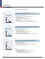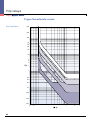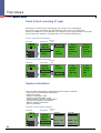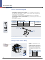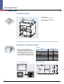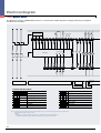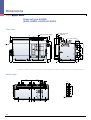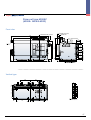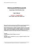
1
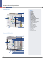
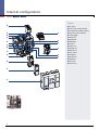
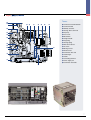
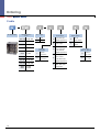
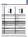
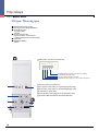
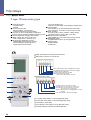
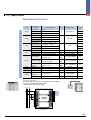
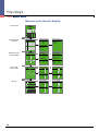
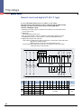
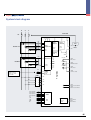
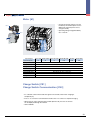
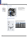
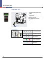
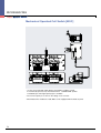
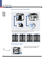
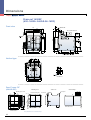
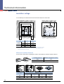
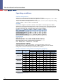
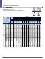
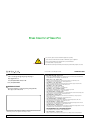
(Marine)
System block diagram
R
S
T
ACB TRIP
AC
Vc
+5
CPU
Output
Display
(LED,LCD)
Vcc/+9V/-9V
CN2CN2-
Filter
Amplicatio
CN2CN2-
SIGNAL CT
MTD
CN2-
Main
PCB
Power
PCB
CN2CN2-
+24
Output
CN2-
Main
PCB
Setting
Part
GND
CN2-
Self power
Vc
RY0 (K1)
CN4-2
PTA contact
+24
POWER
RY1 (K2)
GND
Main
PCB
CN2-
CN4-4
STD/INST contact
+5 V
RY2 (K3)
-5 V
CN4-6
LTD contact
CN4-
Power
PCB
VDM
CN1V
V
V
V
V
V
V
V
CN4-8
Common contact
Trip relay
SMP
CN4-
Additional Source
AC/DC 110~220V
DC 24~48V
CN1CN1CN1-
Input signal (R)
CN3-
Input signal (S)
CN3-
Input signal (T)
Input signal (N)
DC
CN3-
UTX
CN3-
URX
CN3-
CN3-
CN1-5
Remote reset+ terminal
CN1-6
Remote reset- terminal
Test
CN3-
GND
CN3-7/9
AD
CN3-
Main
PCB
Com
Power
PCB
CN4-1
485+ terminal
CN4-3
485- terminal
35