1
Table of Contents
1. Overview of Soldering Technology ................................................................................................. 1
1.1
Soldering Methods .................................................................................................................................................... 2
1.1.1
Types of Soldering Method ............................................................................................................................ 2
1.1.2
Features of the Different Soldering Methods ................................................................................................. 3
1.1.3
Partial Heat Methods ...................................................................................................................................... 4
1.1.4
Total Heating Methods ................................................................................................................................... 6
1.1.5
Adaptation by Package Types ...................................................................................................................... 11
1.1.6
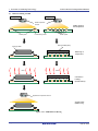
Solder Mounting Processes .......................................................................................................................... 12
1.1.7
Basic Mounting Processes ............................................................................................................................ 12
1.1.8
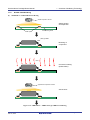
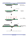
Single-sided Soldering ................................................................................................................................. 13
1.1.9
Double-sided Soldering ................................................................................................................................ 17
2. Printed Wiring Board Design......................................................................................................... 25
2.1
Lead-Type SMDs .................................................................................................................................................... 25
2.1.1
Pin Location Range for Lead-Type SMDs ................................................................................................... 26
2.1.2
Dimensional Examples for Different Package Types................................................................................... 27
2.2
Ball-Type SMD (Including LGA) Packages ........................................................................................................... 36
2.2.1
Pin Positions (Areas) for Ball-Type SMD Packages .................................................................................... 36
2.2.2
Mounting Pad Design for BGA and LGA Packages .................................................................................... 37
2.2.3
Mounting Pad Dimensions (Design Range) ................................................................................................. 37
2.3
THDs....................................................................................................................................................................... 38
2.3.1
THD Pin Location Range ............................................................................................................................. 38
2.3.2
Through Hole Diameter Design ................................................................................................................... 40
2.3.3
Through Hole Diameter Dimensional Design for Printed Wiring Boards (Design Ranges) ........................ 40
2.4
Discrete Devices ..................................................................................................................................................... 41
2.5
Board Materials ....................................................................................................................................................... 41
2.5.1
Preventing Mounting Pad Oxidation ............................................................................................................ 42
2.5.2
Printed Wiring Board Warping .................................................................................................................... 43
2.5.3
Solder Joint Reliability ................................................................................................................................. 43
3. Mounting Processes ....................................................................................................................... 45
3.1
Solder Supply Processes ......................................................................................................................................... 45
3.1.1
Solder Paste .................................................................................................................................................. 45
3.1.2
Solder Paste Printing Processes .................................................................................................................... 48
3.1.3
Amount of Solder Paste Supplied ................................................................................................................ 50
3.2
Component Mounting Processes ............................................................................................................................. 55
3.2.1
Adhesives ..................................................................................................................................................... 55
3.2.2
Component Placement Equipment ............................................................................................................... 55
3.2.3
Self-Alignment Effect .................................................................................................................................. 56
3.3
Soldering Processes ................................................................................................................................................ 64
3.3.1
The Temperature Profile Concept ................................................................................................................ 64
3.3.2
Temperature Profile Conditions ................................................................................................................... 65
3.3.3
Notes on BGA Package Reflow Soldering ................................................................................................... 67
3.3.4
Temperature Distributions in Mixed Mounting............................................................................................ 68
3.4
Cleaning Process ..................................................................................................................................................... 70
3.4.1
Flux Selection............................................................................................................................................... 71
3.4.2
Cleaning Fluid Selection .............................................................................................................................. 71
3.4.3
Selecting the Cleaning Method and Equipment ........................................................................................... 72
3.4.4
Assessment Methods .................................................................................................................................... 73
3.5
Inspection Process ................................................................................................................................................... 74
3.5.1
Visual Inspection Equipment ....................................................................................................................... 75