1
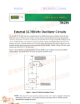
TN235
External 32.768 kHz Oscillator Circuits
An external 32.768 kHz clock is an essential part of any Rabbit-based system. Besides driving the
real-time clock, the 32.768 kHz clock is used by various processor and peripheral subsystems that
are used extensively by Dynamic C software. It is therefore recommended that an external 32.768 kHz
oscillator circuit always be implemented. It is possible to operate the Rabbit without a 32.768 kHz
clock, but several key features will not be available. Without the 32.768 kHz clock, the real-time
clock, the watchdog timer, the periodic interrupt, and asynchronous remote bootstrap will not
function. Neither will any of the low-power features that run off the 32.768 kHz clock.
Figure 1 shows the basic concept behind the external CMOS crystal oscillator circuits used in
Rabbit-based products. The crystal used in the circuit is a parallel resonant crystal.
VBAT
R1
Cin
R1 and R2 control the
power consumed by the
unbuffered inverter.
SN74AHC1GU04
U1A
R2
U2A
NC7SP14
Rp
Rs
CL = 5-12 pF
32.768 kHz
C1
C2
C1 values may vary or
C1 may be eliminated
Figure 1. Basic 32.768 kHz Oscillator Circuit
NOTE: The value of C1 may vary from system to system, or C1 may be completely eliminated
depending on the crystal CL, the amount of frequency deviation from 32.768 kHz, and the
measured drive through the crystal.
022-0084 Rev. E
1
The oscillator is constructed using low-cost single-gate logic. An unbuffered gate is used for the
oscillator because buffered inverters have a tendency to oscillate at higher frequencies and are
prone to startup problems. The output of the oscillator is fed to the Rabbit through a Schmitt trigger buffer. The Schmitt trigger serves two primary functions. First, it prevents power supply or
high-frequency switching noise (primarily from address lines) from getting coupled into the slow
rising clock signal generated by the oscillator; and second, it buffers the output of the oscillator to
generate fast rising/falling (4 ns) square waves.
Internal and External 32.768 kHz Oscillators
The 32.768 kHz oscillator circuit implemented in Rabbit-based systems may vary depending on
the Rabbit processor’s revision and version, low-power requirements, and the type of crystal used.
Table 1 lists the types of crystal oscillator circuits that can be used with each type of Rabbit
microprocessor.
Table 1. 32.768 kHz Crystal Oscillator Circuit Types
32.768 kHz Oscillator
Microprocessor
Internal
Internal
External
Schmitt
Trigger
Rabbit 2000, A–C
Yes
Yes*
Yes†
Rabbit 3000
No
Yes
No
Rabbit 3000A
No
Yes
Yes
* External oscillator is used in low-power applications with
battery backup.
† The Schmitt trigger is part of the on-chip oscillator buffer.
Note that the Rabbit 2000 family of microprocessors contain an internal 32.768 kHz oscillator.
Refer to Chapter 14 of the Rabbit 2000 Microprocessors User’s Manual for more information on
circuit requirements. The internal circuit does not offer the same flexibility as the external circuit
for low-power operation mainly because resistors cannot be placed in series with the power or
ground of the oscillator to limit the switching (crossover) current.
The rest of this technical note will concentrate on external oscillator circuits.
022-0084 Rev. E
2
Rabbit-2000-Based Oscillator and Battery-Backup Circuits
Figure 2 shows the external 32.768 kHz oscillator and battery-backup, and battery-switchover circuits used in Rabbit-2000-based systems. The circuits were designed for low-power operation.
VBAT-EXT
D1
R3
VRAM
2 kW
External Battery
R4
11 kW
Vcc
Rabbit 2000x
VBAT
(pin 42)
D2
R5
10 kW
D4
R6
22 kW
C3
1 nF
C4
1 nF
R1
47 kW
R2
0W
EXT_OSC
U1
Rabbit 2000x
XTALA1
(pin 40)
Rp
22 MW
CONFORMAL
COATING AREA
Rs
Y1
32.768 kHz
C1
10 pF
330 kW
C2
22 pF
Figure 2. Rabbit 2000x 32.768 kHz Oscillator and Battery-Backup Circuits
The current consumption of the circuit is about 4 µA with a 2 V supply. Using this circuit, oscillation continues even when the voltage drops to 0.8 V, and oscillation is still very strong at 1.2 V.
Note that the internal Schmitt trigger of the Rabbit 2000 family of processors does not operate
reliably at voltages below 0.9 V. Furthermore, the oscillator should have its exposed circuit traces
conformally coated to prevent the possibility of loading the circuit by conduction on the PC board
surface in a moist atmosphere. (Rabbit Semiconductor has published an application note on conformal coating, Technical Note TN303, Conformal Coatings.)
022-0084 Rev. E
3
Figure 3 shows the external battery-switchover circuits used in Rabbit-2000-based systems.
VRAM
Vcc
SRAM
Chip Select
VRAM
R11
100 kW
R8*
0W
D
R10* /CSRAM
0W
S
/CS1
Q2
FDV302P G
/RESET
R7
22 kW
R9
10 kW
Q1
MMBT3904
S
D
Q3
FDV302P G
S
D
G
/RESET
* Add resistor R8 to bypass Q2
Add resistor R10 to bypass Q3
Q4
2N7002
C5
1 nF
Figure 3. Rabbit 2000x Battery-Switchover Circuit
022-0084 Rev. E
4
Rabbit-3000-Based Oscillator and Battery-Backup Circuits
Figure 4 shows the external 32.768 kHz oscillator, battery-backup, and battery-switchover circuits
used in Rabbit-3000-based systems found in Z-World and Rabbit Semiconductor board-level
products.
VBAT
RTC Circuit
CLK32K
C3
RESOUT
U2
10 nF
R1
Power to VRAM
Switch
NC7SP14
C4
10 nF
U1
FDV302P
D
R2
22 kW
R3
47 kW
Q1
Rp
22 MW
Y1
CL = 7 pF
C5
100 nF
32.768 kHz
C1
R4
100 W
R5
D1
150 kW
BAT54
VRAM
+3.3 V
0W
SN74AHC1GU04
Rs
330 kW
C2
33 pF
VBAT_EXT
S
G
RESOUT
C6
10 nF
C1 values may vary or
C1 may be eliminated
CONFORMAL
COATING AREA
VRAM
Figure 4. 32.768 kHz Oscillator and Battery-Backup Circuit for Rabbit-3000-Based Systems
The circuit in Figure 4 consumes about 8 µA for a Rabbit 3000 with U2 present and VBAT_EXT
= 3.0 V.
Rabbit-3000A-based systems have special power-up requirements. In these systems, the oscillator
may not start oscillating when the battery is connected for the first time. The input to the internal
Schmitt trigger gets stuck in a region where the Schmitt trigger is unable to latch the data high or
low. Since the oscillator is not running, the output gets stuck somewhere in the linear region
because of Rp. This cycle continues until some amount of random noise disrupts the stability of
the system and kick-starts the oscillator. The stuck condition results in a drop in the battery voltage and an increase in current draw. For the circuit in Figure 4, the current draw measured at R8
increases to 13 µA with the majority of the current going through VBAT. This occurs because R8
is large and is used to provide current to the SRAM, oscillator, and VBAT. The Schmitt trigger
requires a large amount of current at startup, and R8 limits the amount of current available to the
circuit.
022-0084 Rev. E
5
This is not a problem with the circuit in Figure 4 because powering a system only at VBAT_EXT
for a prolonged period doesn’t make any sense and is not normally done. If for some reason a system is only powered at VBAT_EXT (the first time) for a long period of time, the current draw will
not drain the battery significantly. Once main power is applied to the system. the oscillator begins
operating, and when main power is removed, the circuit will switch over to the battery and will
continue to operate reliably.
Note that the circuit in Figure 4 is used for low-power systems. If a Rabbit-3000A-based system
is not battery-backed and the oscillator power consumption is not an issue, the circuit can be simplified as shown in Figure 5 below.
C1 values may vary or
C1 may be eliminated
Vcc = VBAT
CONFORMAL COATING AREA
C3
10 nF
SN74AHC1GU04
CLK32K
U1
Rp
22 MW
Rs
Y1
C1
32.768 kHz
CL = 7 pF
330 kW
C2
33 pF
Figure 5. 32.768 kHz Circuit for Applications not Battery-Backed
For low power circuits, an alternative circuit can be designed that does not exhibit the startup
issue present in the standard circuit shown in Figure 4.
022-0084 Rev. E
6
The circuit in Figure 6 provides separate supplies for the oscillator (VOSC), SRAM (VRAM),
and RTC (VBAT). The circuit consumes about 6.5 µA for VBAT_EXT = 3.0 V, and oscillation
starts at 1.25 V. This solution does not have the startup issue, but is more expensive primarily
because of the extra PMOS transistors.
+3.3 V
CLK32K
D
RESOUT
BAT54
G
S
CONFORMAL
COATING AREA
R3
VBAT_EXT
220 kW
NC7SP14
VOSC
C3
10 nF
R1
0W
+3.3 V
D
RESOUT
G
S
R4
R2
22 kW
VRAM
Rp
22 kW
22 MW
CSRAM = 10 nF
Y1
CL = 7 pF
+3.3 V
32.768 kHz
D
RESOUT
G
S
R5
330 kW
C1
Rs
330 kW
C2
33 pF
VBAT
C1 values may vary or
C1 may be eliminated
C4
10 nF
Figure 6. Alternative Low-Power Circuit for Rabbit-3000A-Based Systems
022-0084 Rev. E
7
Component Selection Guidelines
Rp
The bias resistor, Rp, biases the oscillator buffer (amplifier) to operate in the linear region (VDD/2).
When biased this way, the amplifier has a high gain and will oscillate at the specified frequency.
The recommended value for Rp is between 10 MΩ and 25 MΩ. As the value of Rp increases, the
gain of the amplifier will also increase, enabling the oscillator to start faster and continue operating at a lower voltage.
Rp also limits the short-circuit current when the CMOS gate is switching and thus the overall current consumption.
It is important to note that the 32.768 kHz oscillator circuit draws a very low operating current
and has a high input impedance. The circuit is thus susceptible to noise from nearby high-speed
switching traces and board level contaminants such as dirt and moisture. It is therefore necessary
to protect the oscillator circuit from high-speed switching signals by keeping the oscillator traces
short and using guard traces and copper pours appropriately. Furthermore, the exposed circuit
traces should be conformally coated to protect the circuit from environmental contaminants. Refer
to technical Note TN303, Conformal Coating, for more information.
Rs
The purpose of Rs is to increase the output impedance of the oscillator buffer and limit its drive
current. Rs also affects the amplitude of the voltage swing going into the crystal, and is thus limited by the operating voltage. The value of Rs has to be large enough to prevent the crystal from
being overdriven, but not too large to kill the swing going back into the oscillator. An excessively
large Rs may also cause the circuit to oscillate at an overtone other than that of the fundamental
frequency.
Moderate overdrive of the crystal may be acceptable. However, excessive overdrive may increase
the aging of the crystal and may possibly damage the crystal.
It is somewhat difficult to predict a suitable value for Rs with which to begin. As a starting point,
select a value for Rs such that it has the same impedance as C2 at the operating frequency. From
this point, the value can then be modified to achieve the desired drive level or voltage swing:
1
R s = -------------------------2πf osc * C2
C1, C2
For parallel resonant circuits, the phase shift/load capacitors provide the phase shift and load
capacitance necessary for the oscillator to operate at the tuned frequency. The values of C1 and
C2 can be modified to adjust the oscillator frequency.
022-0084 Rev. E
8
The value of the load capacitors can be calculated in the following manner.
( C1 + C in )* C2
C L = -------------------------------------- + Cs
( C1 + C in ) + C2
In the above equation, Cin represents the input capacitance of the oscillator buffer (roughly 6 to
6.5 pF), CL represents the specified load capacitance of the parallel resonant frequency crystal,
and Cs represents the stray circuit capacitance, which is usually in the range of 2 to 5 pF. Note that
Cin is not constant, but rather is a function of frequency—any measurements of Cin should be done
using a sine wave generator operating at 32.768 kHz.
Ideally C1 and C2 would have equal values because the inverter output introduces a phase shift of
180° and the combination of C1, C2, and the crystal would provide the additional 180° phase shift
required for the phase shift of the loop to equal 360°. However, in reality, the inverter also introduces a phase delay, which creates a phase shift that is somewhat greater than 180°. The capacitors compensate for this phase difference by changing their impedance. This change in impedance
can only occur if the circuit oscillates at a slightly higher frequency than that of the series resonant
frequency of the crystal, which is about 32.765 kHz. In effect, the capacitors pull the oscillation
frequency. The capacitors serve several functions.
• First and foremost, they provide the appropriate load capacitance for the crystal to oscillate at
the correct frequency.
• The capacitors provide the correct amount of phase shift for the circuit to oscillate. Note that
oscillation will not occur if the loop gain is not greater than 1 and if the loop phase shift does
not add up to 360°.
• The RC circuit and the input capacitance of the oscillator buffer control the swing into the
buffer, and the input side capacitance also affects the crystal drive. This affects the power consumption and the maximum operating voltage.
• The capacitors are used to tune the crystal frequency. This is called pullability, and is a function
of the load capacitors.
R1, R2
For low-power applications, these two resistors limit the power consumption of the oscillator buffer
(U1 in Figure 4) by limiting the crossover current during switching. The slower the switching
speed, the longer the transistors stay in the transition region, and thus the greater the crossover
current. Note that the Schmitt trigger does not consume as much current because of its fast switching speed. The key to controlling the current through the oscillator buffer is to limit the amount of
switching current by placing resistors in series with the power and ground of the inverter. These
resistors not only limit the current, but also affect the gain of the oscillator, the startup and stop
voltages, the output duty cycle, and output rise and fall times. The circuit also becomes more susceptible to noise, necessitating the use of the Schmitt trigger. The layout of the oscillator circuit is
therefore extremely important when dealing with such low-current, low-gain, high-input-impedance
circuits. The distances between the Rabbit processor, oscillator buffer, and Schmitt trigger must
be minimized to prevent noise from getting coupled into the circuit.
022-0084 Rev. E
9
Crystal
The 32.768 kHz crystal used in Rabbit-based systems is the same type of crystal as the tuning-fork
quartz crystals used in wristwatches. Table 2 outlines the specifications for these 32.768 kHz crystals.
Table 2. 32.768 kHz Crystal Specifications
Type
—
Through Hole or SMD Tuning-Fork Crystal
Nominal Frequency
F
32.768 kHz
Frequency Tolerance at +25°C
df/F
± 20 ppm
Load Capacitance
CL
7.0–12.5 pF
Series Resistance
RS
50 kΩ (max.)
Drive Level
P
1 µW (max.)
Quality Factor
Q
50,000 (min.)
Turnover Temperature
TT
+ 25°C ± 5°C
Parabolic Curvature Constant
K
-0.04 ppm/°C2 (max.)
Shunt Capacitance
C0
1.4 pF (typical)
Capacitance Ratio
C0/C1
~400 (typical)
Motional Capacitance
C1
0.0035 pF (typical)
Aging
df/F
First year: ± 3 ppm max. at +25°C
Operating Temperature Range
T0
-40°C to +85°C
Storage Temperature Range
TS
-50°C to +125°C
Shock
df/F
5 ppm max.
Vibration
df/F
3 ppm max.
Cut
—
X-Cut
X-cut crystals have a parabolic temperature curve. The maximum frequency variation in tuningfork crystals is roughly -0.04 ppm/°C2. The frequency tolerance at 25°C is typically ± 20 ppm.
Frequency drift per day at 85°C
According to the parabolic temperature curve, the change in frequency at +85°C is -144 ppm.
Since 1 day = 86400 seconds,
86400 seconds/day * (-144 ppm) = -12.44 seconds/day
Frequency drift per day at -45°C
According to the parabolic temperature curve, the change in frequency at -45°C is -196 ppm.
86400 seconds/day * (-196 ppm) = -16.93 seconds/day
NOTE: The -0.04ppm/°C2 parabolic curvature constant is a maximum value. Actual tests of the
crystal yield a drift of -140 ppm (-12.13 seconds/day) at the temperature extremes (-40°C and
+85°C).
022-0084 Rev. E
10
Crystal Drive Level
Typical 32.768 kHz crystals are specified for a maximum drive level of 1 µW. A modest overdrive, perhaps 100% over this limit, will most likely not have any adverse effect except to cause
the crystal to age more rapidly. Aging in a crystal is exhibited as a gradual change of frequency,
about 3 parts per million, and is most significant in the first few months of operation.
The drive power can be computed from P = (I2)*R, where I is the rms AC current and R is the
effective resistance of the crystal. Typical values for R are 25 kΩ for 32.768 kHz turning-fork crystals. Maximum values are often specified as 35 kΩ or 50 kΩ. If the effective resistance is 25 kΩ,
then 1 µW of power is reached when I = 6.3 µA (rms). It is logical to use the typical effective
resistance rather than the maximum total resistance in computing drive-power. If a particular crystal has a higher resistance, it requires more power to sustain the same amplitude of physical flexure of the quartz. This indicates that the stress on the quartz will not be greater even though the
drive power is greater for a unit that happens to have an effective resistance of 35 kΩ rather than
the typical value of 25 kΩ.
In calculating the current through the crystal, the output capacitance of the buffer is not relevant
because the resistor Rs isolates it from the crystal. C1, however, is very important. If C1 is made
smaller, this will increase the voltage swing on the gate input of the oscillator buffer and will
allow the oscillator to operate at a lower voltage. This oscillator will start at about 1.2 V and operate down to about 0.75 V.
The current can be measured directly with a sensitive current probe, but it is easier to calculate the
current by measuring the voltage swing at the gate input with a low-capacitance oscilloscope
probe. The rms voltage at this point is related to the rms current by the relationship
I = Vrms*ω*Ctot
where
Ctot = C1 + CIn + Cprobe
ω = 2π(32768)
Vrms = 0.707(Vp-p)
If Ctot = 12 pF (assuming Cprobe = 1 pF) and the effective resistance is 25 kΩ, then the current in
(µA) and the drive power in (µW) are given by the following approximation.
I = 2.5*Vrms
P = 0.1*(Vrms)2
or
I = 1.75*Vp-p
P = 0.05*(Vp-p)2
Based on the above equations and calculations,
P = 1.25 µW for a 5.0 V (p-p) swing,
P = 0.65 µW for a 3.6 V (p-p) swing, and
P = 0.45 µW for a 3.0 V (p-p) swing.
022-0084 Rev. E
11
From the above analysis it is clear that the value of C1 greatly affects the crystal drive level. The
value of C1 depends on the crystal load capacitance, CL. For this reason, Rabbit-based systems
use crystals with low CL requirements. Currently, Rabbit-2000 and 3000-based systems use
crystals with a load capacitance of 7 pF.
Summary of Values for Rabbit-Based 32.768 kHz Oscillators
Component
Value
Rp
10–25 MΩ
Rs
330–680 kΩ
Limits drive current (crystal-drive level ~ 1 µW)
CL
6.0–12.5 pF
Parallel resonant crystal load capacitance
C1
0–15 pF
C2
15–33 pF
R1, R2
2–22 kΩ
Notes
Affects gain
The values can be used to tune the oscillator frequency, and may
vary depending on the crystal load capacitance used. Appropriate
values can be determined through calculations and optimized
through experimentation.
Approved Manufacturers List
Component
Crystal
Manufacturer
Part Number
Contact
ECS
ECS-0327-6-17
http://www.ecsxtal.com
ILSI
IL3R-HX5F7-32.768
http://www.ilsiamerica.com
Seiko Instruments SSPT7-.032768-7pF
http://www.siielectroniccomponents.com
Texas Instruments SN74AHC1GU04DBVR http://www.ti.com
Unbuffered
Inverter
Schmitt Trigger
Fairchild
Semiconductor
NC7SU04M5
NC7SZU04P5
http://www.fairchildsemi.com
On
Semiconductor
NL17SZU04DF
http://www.onsemi.com/home
Fairchild Semi.
NC7SP14P5
http://www.fairchildsemi.com
022-0084 Rev. E
12
References
Marvin E. Ferking, Crystal Oscillator Design and Temperature Compensation, Van Norstrand Reinhold Company, New York, 1978.
Benjamin Parzen, Design of Crystal and other Harmonic Oscillators, John Wiley and Sons, Inc., New York,
1983.
Norman L. Rogers, Rabbit Semiconductor.
David Salt, HY-Q Handbook of Quartz Crystal Devices, Van Norstrand Reinhold (UK) Co. Ltd., 1987.
Z-World, Inc.
Rabbit Semiconductor
2900 Spafford Street
Davis, California 95616-6800
USA
2932 Spafford Street
Davis, California 95616-6800
USA
Telephone: (530) 757-3737
Fax: (530) 757-3792
Telephone: (530) 757-8400
Fax: (530) 757-8402
www.zworld.com
www.rabbitsemiconductor.com
022-0084 Rev. E
13