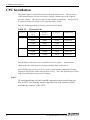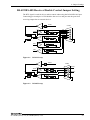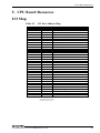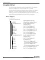
1
SBC Series
NLX BUS SBC for Socket370 CPU
with LAN/VGA
PC-686BX(NLX)-LV
PC-686BX(NLX)-LVV
User’s Manual
CONTEC CO.,LTD.
Copyright
Copyright 2001 CONTEC Co., LTD. ALL RIGHTS RESERVED
No part of this document may be copied or reproduced in any form by any means
without prior written consent of CONTEC Co., LTD.
CONTEC Co., LTD. makes no commitment to update or keep current the information
contained in this document.
The information in this document is subject to change without notice.
All relevant issues have been considered in the preparation of this document.
Should
you notice an omission or any questionable item in this document, please feel free to
notify
CONTEC Co., LTD.
Regardless of the foregoing statement, CONTEC assumes no responsibility for any
errors that may appear in this document nor for results obtained by the user as a result
of using this product.
Trademarks
MS, Microsoft, MS-DOS and Windows are trademarks of Microsoft Corporation.
Other brand and product names are trademarks of their respective holder.
PC-686BX(NLX)-LV, PC-686BX(NLX)-LVV
i
Product Configuration
- CPU board
(PC-686BX(NLX)-LV or PC-686BX(NLX)-LVV) ... 1
- Manual (this booklet)... 1
- IDE 40-pin ribbon cable ... 1
- Floppy disk ribbon cable ... 1
- Bracket for attaching serial port (2x male D-SUB 9-pin) ribbon
cable ... 1
- Bracket for attaching parallel port (1x female D-SUB 25-pin)
ribbon cable ... 1
- Driver disk utility (CD-ROM) ... 1
- Jumper pins ... 6
- 5-pin DIN to 6-pin MINI-DIN keyboard converter cable ... 1
Unpacking:
This board is specially packed in an anti-static bag to prevent damage in shipping.
Check the contents to make sure that you have everything listed above.
If you do
not have all the items, contact your distributor or CONTEC group office where you
purchased.
Note!
Do not remove the board from its protective packaging until the
computer case is open and ready for installation. Electrical static
can cause damage to electrical components.
ii
PC-686BX(NLX)-LV, PC-686BX(NLX)-LVV
Table of Contents
Copyright............................................................................ i
Trademarks ........................................................................ i
Product Configuration ...................................................... ii
1. Introduction ..................................................................1
Features ........................................................................ 1
Limited Three-Years Warranty.................................... 2
How to Obtain Service.................................................. 3
Liability......................................................................... 3
Warning......................................................................... 3
Handling Precautions................................................... 3
Structure of This Manual............................................. 4
2. Specifications ................................................................5
Functional Specifications ............................................. 5
General Specifications.................................................. 6
Power Management.......................................................... 7
Power Supply Requirements ............................................ 9
Power Consumption ..................................................... 9
Board Component Names............................................... 10
Block Diagram ................................................................ 11
3. Hardware Description ................................................. 13
Installation Procedure .................................................... 13
CPU Installation............................................................. 14
Main Memory Installation:DIMM1 and DIMM2 .......... 15
SDRAM............................................................................ 15
Parallel Port Connector: CN1 ........................................ 16
Serial Port Connector: CN2/CN3 ................................... 17
RS-422 / RS-485 Specifications.................................. 18
USB Connector: CN4 ...................................................... 19
Keyboard Connector: CN11 ............................................ 20
PS/2 Mouse Connector: CN6 .......................................... 21
RJ-45 LAN Connector: CN12 ......................................... 21
LCD Connector: CN5 ...................................................... 22
VGA Connector: CN7 ...................................................... 23
CPU Fan Connector: CN9 .............................................. 23
PC-686BX(NLX)-LV, PC-686BX(NLX)-LVV
iii
External Battery Connector: CN10 ............................... 24
4. Jumper Settings ......................................................... 25
Watchdog Timer Output Selector: JP6 .......................... 25
RS-232C/422/485 Selector Switch: JP1/JP2 .................. 26
Transmit Data Control for Half-Duplex Mode.......... 26
RS-422/RS-485 Receiver Disable Control
Jumper Setting ............ 27
I/O Addresses and Commands ................................... 28
RS-422/485 Terminating Resistance: JP3 ..................... 28
On-Board LAN Selector: JP7 ......................................... 29
Disk On Chip Memory Address Selector: JP4............... 29
Display Type Setting: JP5.............................................. 30
CMOS Memory Erase: JP8 ............................................ 31
On Board VGA Selector: JP9 ......................................... 31
POWER Supply AT/ATX Selector: JP10........................ 32
LED Display: .................................................................. 32
5. CPU Board Resources................................................. 33
I/O Map ........................................................................... 33
Memory Map................................................................... 34
DMA Channels................................................................ 34
PCI Configuration Space Map ....................................... 35
Interrupts........................................................................ 35
PCI Interrupt Routing Map ........................................... 36
6. Software Utilities ....................................................... 39
Intel 440BX Chipset Driver ........................................... 39
INF Installation Utility ............................................. 39
Graphics Driver .............................................................. 40
Driver Support............................................................ 40
LAN Driver ..................................................................... 41
Watchdog Timer (WDT) Setup ....................................... 43
Upgrading the BIOS to a New Version.......................... 44
Hardware Monitoring..................................................... 45
7.
BIOS Setup .............................................................. 53
Main Menu...................................................................... 56
Standard CMOS Setup................................................... 58
iv
PC-686BX(NLX)-LV, PC-686BX(NLX)-LVV
BIOS Features Setup...................................................... 61
Chipset Features Setup.................................................. 65
Integrated Peripherals ................................................... 69
Power Management Setup ............................................. 72
PnP/PCI Configuration Setup ........................................ 76
Defaults Menu ................................................................ 79
Load BIOS Defaults ................................................... 79
Load SETUP Defaults ................................................ 79
Supervisor/User Password Setting ................................ 79
Exit Options .................................................................... 81
POST Messages .............................................................. 82
POST Alarm Tones.......................................................... 82
Error Messages ............................................................... 83
POST Codes .................................................................... 89
8. Available Accessories ................................................... 95
PC-686BX(NLX)-LV, PC-686BX(NLX)-LVV
v
vi
PC-686BX(NLX)-LV, PC-686BX(NLX)-LVV
1. Introduction
1. Introduction
Thank you for purchasing the PC-686BX(NLX) board.
The PC-686BX(NLX) is a single-board computer supporting Intel Celeron 300MHz
and higher and Pentium III 500MHz and higher processors.
Please read this manual carefully before connecting to external devices and
configuring systems.
This product is a NLX standard industrial CPU board developed using Intel’s 440BX
chipset and designed for use in harsh industrial environments. A feature of the board
is the use of the socket 370 which is compatible with Intel processors.
The board supports a maximum of 512MB of SDRAM memory.
The board also incorporates an on-board CPU temperature sensor (Winbond W83781D
chipset) to detect processor heating. The circuit complies with the management
(WFM) 2.0 specifications.
The board has a LAN connector that uses the Intel 82559 PCI LAN controller.
The board has an LCD connector that uses the Chips 69030 graphics accelerator
(Chips 69000 only PC-686BX(NLX)-LV).
Features
- Uses the NLX standard for full PC/AT compatibility
- Supports the Intel Celeron and Pentium III CPUs (Socket 370)
- Uses the Award 2MB flash BIOS
- Supports up to 512MB of SDRAM RAM using 2 x DIMM memory
sockets
- Two IDE connectors (Supports up to four extended IDE drives)
- Boot from A, C, D, E, SCSI, CD-ROM, ZIP, or LS selectable via
the BIOS
PC-686BX(NLX)-LV, PC-686BX(NLX)-LVV
1
1. Introduction
- Incorporates an AGP bus C&T 69030 VGA and flat panel
controller board with 4MB VRAM providing full IBM VGA
compatibility (used for PC-686BX(NLX)-LVV), or incorporates an
AGP bus C&T 69000 VGA and flat panel controller board with
2MB VRAM providing full IBM VGA compatibility (used for PC686BX(NLX)-LV). Panel type configurable by H/W or S/W.
- On-board floppy disk drive controller
(720KB/360KB/1.44MB/2.88MB)
- Two serial ports with FIFO function. COM2 is jumper-selectable
between RS-232C, RS-422, and RS-485
- Bi-directional parallel port (supports ECP/EPP mode)
- PS/2 mouse port (MINI-DIN 6-pin)
- Supports the Disk On Chip from M-Systems (selectable expansion
BIOS address)
- Watchdog timeout is software-selectable in the range 0 to 30
seconds (16 levels). Timeout triggers a system reset or NMI.
- Realtime clock and CMOS are backed up by an integrated battery.
- Incorporates a PCI interface 10/100M Ethernet connection (RJ-45
port)
- Supports two USB port interfaces
- PS/2 keyboard (MINI-DIN 6-pin)
Limited Three-Years Warranty
CONTEC Interface boards are warranted by CONTEC Co., LTD. to be free from
defects in material and workmanship for up to three years from the date of purchase by
the original purchaser.
Repair will be free of charge only when this device is returned freight prepaid with a
copy of the original invoice and a Return Merchandise Authorization to the distributor
or the CONTEC group office, from which it was purchased.
This warranty is not applicable for scratches or normal wear, but only for the electronic
circuitry and original boards.
The warranty is not applicable if the device has been
tampered with or damaged through abuse, mistreatment, neglect, or unreasonable use,
or if the original invoice is not included, in which case repairs will be considered
beyond the warranty policy.
2
PC-686BX(NLX)-LV, PC-686BX(NLX)-LVV
1. Introduction
How to Obtain Service
For replacement or repair, return the device freight prepaid, with a copy of the original
invoice.
Please obtain a Return Merchandise Authorization Number (RMA) from the
CONTEC group office where you purchased before returning any product.
* No product will be accepted by CONTEC group without the RMA
number.
Liability
The obligation of the warrantor is solely to repair or replace the product. In no event will
the warrantor be liable for any incidental or consequential damages due to such defect or
consequences that arise from inexperienced usage, misuse, or malfunction of this device.
Warning
Replacing with an incorrect battery is dangerous and may result in explosion.
Always replace with a battery of the same type or the manufacturer’s recommended
equivalent type.
Please dispose of the old battery in accordance with the
manufacturer’s instructions.
Handling Precautions
Take the following precautions when handling this product.
- Do not modify the board. CONTEC accepts no responsibility for
modified products.
- Do not subject the board to impact, bending, or other physical force
as this may damage the board.
- Do not touch the metal plated terminals (edge connectors) on the
board as this can cause bad connections. If you do touch these
connectors, clean using industrial alcohol.
- The board contains a number of switches that must be set in
advance. Check that these are set correctly before installing the
board.
- Do not set the board switches or jumpers to settings other than
those described in the documentation as this may damage the
board.
PC-686BX(NLX)-LV, PC-686BX(NLX)-LVV
3
1. Introduction
- Install the board in an NLX bus expansion slot on the backplane
board.
- Do not insert or remove the board from the slot while the main
power is turned on as this may damage the board. Always turn off
the power to the PC beforehand.
- The total current drawn by the boards installed in the backplane
expansion slots may not exceed the power supply capacity of the
PC. Excess load can result in damage.
Structure of This Manual
Chapter 1
Introduction
Chapter 2
Specifications
Describes specifications relating to the use of the board, operating
environment restrictions, and the names of each component.
Chapter 3
Hardware Description
Explains the setup procedure and describes the various board
connectors.
Chapter 4
Jumper Settings
Describes the jumpers and other board settings.
Chapter 5
CPU Board Resources
Lists the I/O board addresses, interrupt request lines (IRQ), and similar
information.
Chapter 6
Software Utilities
Describes the software utilities provided with the board.
Chapter 7
BIOS Setup
Describes the BIOS settings.
Chapter 8
4
Available Accessories
PC-686BX(NLX)-LV, PC-686BX(NLX)-LVV
2. Specifications
2. Specifications
Functional Specifications
Table 2.1.
Functional Specifications
Item
Processor socket
CPU (Option)
Bus speed
Cache
<1/2>
Specification
Socket370
Intel Celeron 300 to 850MHz
Pentium III 500 to 850MHz (FSB100MHz)
66 MHz/100 MHz
Celeron CPU contains internal 128KB L2 cache
Pentium III CPU contains internal 256KB L2 cache
Memory (Option)
Max. 512MB 168-pin DIMM socket x 2 SDRAM PC100
Chipset
Intel 440BX
C&T 69030 controller (PC-686BX(NLX)-LVV)
VGA
C&T 69000 controller (PC-686BX(NLX)-LV)
CRT connector: VGA compatible HD-SUB 15-pin
CMOS data backed up by Lithium battery (CR2032)
The following table lists the Lithium battery specifications (button-type)
Realtime clock
/calendar
Specification
CR2032
Voltage
3V
Capacity
220mAh
Weight
3.1g
Please change the CR2032 battery when it goes
down under 2.3V.
If you don't change it, when booting system, CMOS
Checksum Error occurs and OS doesn't boot, and
when Power off, RTC maybe stopped.
The battery backup term of CR2032 is 3.0 years or more.(In main power is off.)
Award BIOS, includes Plug&Play (PnP)
BIOS
512KB flash EEPROM
Power management: Uses ACPI
CPU frequency/voltage control (Not modifiable)
Keyboard/mouse
connector
PS/2 keyboard
PS/2 mouse
1 x 5-pin expansion keyboard connector
2 x 16550 compatible UARTs
COM1 : RS-232C
Serial ports
(Includes 10-pin header connector -> D-SUB 9-pin (male) conversion cable)
COM2 : RS-232C/422/485
(Includes 10-pin header connector -> D-SUB 9-pin (male) conversion cable)
Parallel port
1 x SPP, ECP, EPP high speed parallel port
(Includes 26-pin header connector -> D-SUB 25-pin cable)
IDE interface
2 x EIDE ports, Max. 4 x IDE devices UltraDMA/33 connected to NLX BUS
FDD interface
Supports 2 x drives (360K/720K/1.2M/1.44M/2.88M/LS-120), Connected to NLX BUS
SSD socket
Supports M-Systems DiskOnChip 2 - 144MB
PC-686BX(NLX)-LV, PC-686BX(NLX)-LVV
5
2. Specifications
Table 2.1.
Functional Specifications
Item
<2/2>
Specification
Intel 82559
LAN interface
1 x RJ-45 connector
Wake On LAN support (Only when ATX power supply used)
USB interface
Supports 2 x USB ports pin header 10-pin (USB connector cable sold separately)
Timeout settings :
Watchdog
Selectable 0, 2, 6, 8, 10, 12, 14, 16, 18, 20, 22, 24, 26, 28, or 30 seconds
Generates reset or NMI on timeout
DMA
Chipset includes 2 x 82C37 equivalent, 7 channels
Interrupts
Chipset includes 2 x 82C59 equivalent, 15 levels
Expansion bus
NLX BUS
Super I/O
Winbond W83977TF
Monitoring IC
Winbond W83781D
General Specifications
Table 2.2. General Specifications
Item
6
Specification
Current consumption
(For Celeron 733MHz )
+5VDC 10A
+12VDC 200mA
+5VSB (standby) 300mA
(For Pentium III 850MHz )
+5VDC 12A
+12VDC 200mA
+5VSB (standby) 300mA
Ambient temperature (storage)
-40 to +80°C
Ambient temperature (operation)
0 to +60°C
Ambient humidity
20 to 80%RH (No condensation)
Suspended particles
Not especially severe
Corrosive gases
None
System power supply
requirements
DC voltage : +5V (+4.75 - +5.25V)
DC voltage : +12V (+11.4 - +12.6V)
External dimensions (mm)
122(L)×220(W)
Weight
380g
PC-686BX(NLX)-LV, PC-686BX(NLX)-LVV
2. Specifications
Power Management
The PIIX4 power management function provides system designers with a range of
different functions and configuration options for implementing various power saving
modes.
PIIX4 performs the following four general types of power management.
- Clock control and processor complex management
- Peripheral device management
- System management (SMI generation, system management bus)
- System shutdown and restart
The following gives a brief explanation of the main power management functions.
Clock Control
The processor complex (processor, host bridge, DRAM, and L2 cache) does not need
to execute cycles when the operating system (OS), application program, and system
software are not performing any useful work.
At times such as this, the system can
go into standby mode.
Peripheral Device Management
Peripheral resources are monitored to detect when particular devices are idle.
The
system power management software can set the power management state (local
standby or power off, etc.) of individual devices.
PIIX4 notifies specific devices to
the system power management software for monitoring.
System Shutdown
On determining that the system is completely idle or when a significant system event
has occurred, the system power management software can shutdown the system.
provides a significant saving in power consumption.
This
The software specifies
shutdown event, restart event and wakeup event settings to PIIX4 and PIIX4
automatically changes the system to the shutdown state in accordance with these
settings.
Similarly, PIIX4 automatically restarts operation when a valid restart event
is detected.
PC-686BX(NLX)-LV, PC-686BX(NLX)-LVV
7
2. Specifications
- Three different shutdown states are available:
- Power-on shutdown (POS) (Three system reset options are
provided.)
- RAM shutdown (STR)
- Disk shutdown (STD) or software OFF (Soff)
- Long duration standby timer used as a restart timer to monitor the
overall idle state of the system
(Continues to operate during shutdown)
- Power button input
- An override function that changes immediately to the software
OFF mode.
- Shadow registers for the standard AT write-only registers are used
to save and restore the system state
- "Resume Well" function monitors for wakeup events during
shutdown
- Power-on restart and reset procedures
8
PC-686BX(NLX)-LV, PC-686BX(NLX)-LVV
2. Specifications
Power Supply Requirements
A clean and stable power supply is required to ensure reliable operation due to the high
CPU clock frequencies used on the board. The quality of the power supply is even
more important.
To achieve the maximum performance from such high-speed CPUs, ensure that the DC
power supply remains within the range 4.75V to 5.25V.
Power Consumption
In its standard configuration, the CPU board is designed to operate with at least a
200W power supply.
If a high-load configuration is used, a power supply with
greater than 200W capacity is required. The power supply must satisfy the following
requirements.
- Power supply rise time: 2ms to 20ms
- Minimum delay in response to a reset on a good-quality power
supply: 100ms
- Minimum power supply disconnect warning: 1ms
- The 3.3V output must reach the minimum fluctuation ratio level
within 20ms of the +5V output reaching its minimum fluctuation
ratio level.
The table below lists the DC voltage tolerances for the power supply.
Table 2.3.
DC Voltage Tolerances
DC Voltage
Tolerance
+3.3V
±5%
+5V
±5%
+5VSB (standby)
±5%
-5V
±5%
+12V
±5%
-12V
±5%
PC-686BX(NLX)-LV, PC-686BX(NLX)-LVV
9
2. Specifications
Board Component Names
DIMM1
DIMM2
CN1
CN2
CN3
CN4
JP1
JP2
J1
CN5
JP3
LAN
JP6
JP4
MOUSE
CN8
JP5
CN9
JP9
JP8
JP10
CN10
JP7
VGA
KEY
J1, CN8 are not used.
Please do not connect anything.
Figure 2.1.
10
Component Names
PC-686BX(NLX)-LV, PC-686BX(NLX)-LVV
2. Specifications
Block Diagram
VRM
SOCKET370
CLK GEN.
443BX
DIMM x 2
GTL+BUS
GTL
NLX GOLDEN FINGER
TERMINATOR
PCI bus
USB #1, #2
PIIX4E
LAN
VGA
(82371EB)
(82559)
(69030 /
69000 *)
IDE #1, #2
ISA bus
COM #1, #2
BIOS
FDD
H/W
MONITOR
SUPER I/O
(W83977TF)
KB / MS
LPT
* 69000 is used for PC-686BX(NLX)-LV.
Figure 2.2.
Block Diagram
PC-686BX(NLX)-LV, PC-686BX(NLX)-LVV
11
2. Specifications
12
PC-686BX(NLX)-LV, PC-686BX(NLX)-LVV
3. Hardware Description
3. Hardware Description
This chapter describes the board jumper settings and connectors required to setup the
board for operation.
Installation Procedure
(1) Install the processor making sure it is oriented correctly.
(2) Install the DRAM modules making sure they are oriented
correctly.
(3) Attach the fan above the processor and plug into the fan
connector.
(4) Insert all external cables other than for the flat panel
(VGA, hard disk, floppy, keyboard, mouse, LAN, etc.)
(5) Connect a CRT monitor to use for the CMOS setup.
(6) Confirm that the backplane power is turned off.
(7) Insert the CPU board into the backplane.
(8) Turn on the power.
(9) As the system starts to boot, hold down the DEL key to enter
BIOS setup mode.
(10) Set the peripheral setup and standard setup to the correct
settings.
Note!
The CMOS memory may be initialized to an undefined state if the
non-battery backup period has elapsed.
“Cmos Checksum error” may be founded when you are using at first time.
When will
you find it , please hold down the DEL key to Setup BIOS .
PC-686BX(NLX)-LV, PC-686BX(NLX)-LVV
13
3. Hardware Description
CPU Installation
The board supports a single Intel Celeron or Pentium III processor. The processor’s
VID pin automatically sets the CPU board’s voltage variation ratio to the required
processor voltage. The host bus speed is also selected automatically.
The processor
is connected to the CPU board via a 370-pin ZIF PPGA socket.
The CPU board supports the processors listed in the table below.
Table 3.1.
Processor
Celeron
Pentium III
Processor List
Processor
Host Bus
Speed
Frequency
Cache Size
CONTEC Model
433MHz
66MHz
128KB
--
566MHz
66MHz
128KB
PC686C-566
733MHz
66MHz
128KB
--
850MHz
100MHz
128KB
PC686C-850
600MHz
100MHz
256KB
--
700MHz
100MHz
256KB
PC686-700
850MHz
100MHz
256KB
PC686-850
The ZIF PPGA socket has a lever to hold the processor in place.
Ensure that the
notch on the side of the processor is aligned with the notch in the socket.
After installing the processor in the 370 socket, check that the configuration settings
relating to the processor model and speed are correct. The CPU must always be fitted
with a heat sink and fan to prevent overheating.
Note!
To avoid problems such as unstable operation and system hang-up
due to CPU overheating, ensure that the heat sink contacts firmly
with the top surface of the CPU.
14
PC-686BX(NLX)-LV, PC-686BX(NLX)-LVV
3. Hardware Description
Main Memory Installation: DIMM1 and DIMM2
The board provides two dual in-line memory module (168-pin DIMM) sockets giving
a maximum memory size of 512MB.
The BIOS determines the SDRAM size and speed using in the serial presence
detection (SPD) data structure set in E2PROM on the DIMM.
The minimum
memory size is 32MB and the maximum is 512MB. The memory size and speed can
be different for each socket.
The CPU board supports the following memory functions.
- 168-pin DIMM, metal plated earth
- 100MHz SDRAM (PC-100)
- Non-ECC (64-bit) or ECC (72-bit) memory
- 3.3V memory only
- Unbuffered single-port or dual-port DIMMs in the following sizes
SDRAM
Synchronous DRAM (SDRAM) achieves improved memory performance by
performing memory access synchronized by the memory clock.
Whereas SDRAM
can achieve burst transfer speed with x-1-1-1 timing, asynchronous memory subsystems are generally restricted to x-2-2-2 transfer speed.
The CPU board supports single-port or dual-port DIMMs in the following sizes.
Table 3.2.
SDRAM
DIMM Size
Non-ECC
32MB
4Mbit×64
ECC
---
64MB
8Mbit×64
8Mbit×72
128MB
16Mbit×64
16Mbit×72
256MB
32Mbit×64
32Mbit×72
Note!
All memory components and DIMMs used with this board must
comply with the PC SDRAM specification. The PC SDRAM
specification specifies the specifications for PC SDRAM (specific to
memory components), the specifications for DIMMs with no PC
buffer, PC serial presence detection specifications, and similar.
PC-686BX(NLX)-LV, PC-686BX(NLX)-LVV
15
3. Hardware Description
Parallel Port Connector: CN1
The parallel port bracket can be used to add an additional parallel port for connecting
additional parallel devices. The following four options are provided for parallel port
operation.
- Compatible (Standard mode)
- Bidirectional (PS/2 compatible)
- Bidirectional EPP.
A driver must be provided by the peripheral device manufacturer to
use this mode.
- Bidirectional high-speed ECP
Table 3.3.
CN1: Parallel Port Connector
Pin layout after conversion by cable provided (D-SUB 25-pin)
CN1
1
25
16
2
26
Pin No.
Function
Pin No.
Function
Pin No.
Function
Pin No.
1
STROBE
2
ALF
1
STROBE
14
ALF
3
PD0
4
ERROR
2
PD0
15
ERROR
5
PD1
6
INIT
3
PD1
16
INIT
7
PD2
8
SLCT IN
4
PD2
17
SLCT IN
1
14
Function
9
PD3
10
GND
5
PD3
18
GND
11
PD4
12
GND
6
PD4
19
GND
13
PD5
14
GND
7
PD5
20
GND
15
PD6
16
GND
8
PD6
21
GND
17
PD7
18
GND
9
PD7
22
GND
19
ACK
20
GND
10
ACK
23
GND
21
BUSY
22
GND
11
BUSY
24
GND
23
PE
24
GND
12
PE
25
GND
25
SLCT
26
N.C.
13
SLCT
13
25
PC-686BX(NLX)-LV, PC-686BX(NLX)-LVV
3. Hardware Description
Serial Port Connector: CN2/CN3
COM1 (CN2) and COM2 (CN3) are on-board serial ports with 10-pin box head
connectors.
The table below shows the pin layout for these connectors.
Table 3.4.
COM2(CN3)
Serial Port Connector
CN3
1
6
5
10
COM1(CN2)
PIN
RS-232C
RS-422
RS-485
PIN
RS-232C
1
DCD
TX-
TX-
1
DCD
2
RXD
TX+
TX+
2
RXD
3
TXD
RX+
RX+
4
DTR
RX-
RX-
5
GND
GND
6
DSR
RTS-
7
RTS
RTS+
N.C.
8
CTS
CTS+
9
RI
10
N.C.
CN2
3
TXD
4
DTR
GND
5
GND
N.C.
6
DSR
7
RTS
N.C.
8
CTS
CTS-
N.C.
9
RI
N.C.
N.C.
10
N.C.
1
5
6
10
In case of using the accessory Cable (D-SUB 9pin)
1
5
6
9
RS-485
PIN
RS-232C
RS-422
1
DCD
TX-
TX-
2
RXD
TX+
TX+
3
TXD
RX+
RX+
4
DTR
RX-
RX-
5
GND
GND
GND
6
DSR
RTS-
N.C.
7
RTS
RTS+
N.C.
8
CTS
CTS+
N.C.
9
RI
CTS-
N.C.
Notes!
- For RS-485, TX+ (pin 2) and RX+ (pin 3) must be connected by a
jumper in the D-type connector.
- The same applies for TX- (pin 1) and RX- (pin 4).
PC-686BX(NLX)-LV, PC-686BX(NLX)-LVV
17
3. Hardware Description
RS-422 / RS-485 Specifications
- Transmission system: Half or full duplex serial transfer complying
with RS-422 or RS-485
- Baud rate: 19200 to 50 bps (Selectable)
- Signal transmission distance: 1.2km max.
Note!
The mouse and keyboard can be plugged into either PS/2 connector.
However, the power must be turned off before connecting or
disconnecting the keyboard or mouse.
The keyboard controller includes code for old-style keyboard and mouse control
functions and also supports password protection of power-on and reset. The poweron and reset password is specified using the BIOS setup program.
The keyboard controller also supports the <Ctrl><Alt><Del> hotkey sequence and
software reset.
This hotkey sequence jumps to the start of the BIOS code and
executes the power-on self test (POST) function to reset the computer’s software.
Infra-Red Support
The front panel I/O connector includes 6 pins that support a Hewlett Packard HSDL1000 compatible infra-red (IR) transceiver.
Serial port B can be assigned to the connected IR device using the setup program.
this case, the serial port B connector can no longer be used.)
(In
IR connections can be
used for file transfer with mobile devices such as laptops, PDAs, and printers.
The Infra-Red Data Transfer Standards Association (IrDA) specifications support
115Kbit/sec data transfer at a range of 1m.
Consumer Infra-Red Support
The front panel I/O connector includes a pin that supports a consumer infra-red device
(remote control). This pin supports reception only with data transfer rates up to
685.57Kbit/sec.
Consumer infra-red devices can be used to control telephone or multimedia operation
such as changing the volume or CD track.
For the computer to support consumer
infra-red devices both a software interface and hardware interface are required.
18
PC-686BX(NLX)-LV, PC-686BX(NLX)-LVV
3. Hardware Description
USB Connector: CN4
The universal serial bus (USB) is able to automatically detect plug and play computer
peripherals (such as a keyboard, mouse, joystick, scanner, printer, modem/ISDN, CDROM, or floppy disk drive) when they are physically connected without the need to
reboot or install a driver.
The USB connector can be used to connect any of a number of USB devices to the
computer.
Normally, the device driver for the USB device is managed by the
operating system (OS).
However, as keyboard and mouse support is required for the
Setup program before the operating system (OS) boots, the BIOS also supports a USB
keyboard and mouse.
The CPU board has two USB ports and one USB peripheral can be connected to each
port. To connect three or more USB devices, an external hub can be connected to
either of the USB ports.
The CPU includes full support for the universal host controller interface (UHCI) and
uses UHCI compatible software drivers.
The USB functions are as follows.
- Self-identifying peripheral devices can be plugged in while
computer is running (USB Ver.1.1)
- Automatic mapping to driver and configuration functions
- Supports synchronous and asynchronous operation on the same
wire set
- Supports a maximum of 127 physical devices
- Guaranteed bandwidth and short delay time suitable for telephone,
audio and similar applications
- Error handling and fault handling mechanisms are included in the
protocol
Note!
Computer systems may not comply with FCC class B requirements if
a non-approved cable is connected to the USB port, even if no device
is connected to the cable or only a low-speed device is connected.
Always use a cable that meets the requirements of the highest speed
devices.
PC-686BX(NLX)-LV, PC-686BX(NLX)-LVV
19
3. Hardware Description
Table 3.5.
CN4: USB Connector
CN4
2
10
1
9
Function
Pin No.
Function
Pin No.
1
VCC
2
VCC
3
USBP0-
4
USB1-
5
USBP0+
6
USB1+
7
USBG
8
USBG
9
GND
10
GND
Refer to "Chapter 8. Available Accessories" for a list of USB connector cables.
Keyboard Connector: CN11
The CPU board has a standard PS/2 keyboard MINI DIN connector for attaching the
keyboard. The keyboard can be plugged directly into this connector. The connector
pin layout is shown below.
Table 3.6.
CN11: Keyboard Connector
CN11
6
5
4
3
2
20
1
Pin No.
Function
1
K.B DATA
2
N.C.
3
GND
4
+5V
5
K.B CLOCK
6
N.C.
PC-686BX(NLX)-LV, PC-686BX(NLX)-LVV
3. Hardware Description
PS/2 Mouse Connector: CN6
The CPU board has a standard PS/2 mouse MINI DIN connector for attaching a PS/2
mouse.
The PS/2 mouse can be plugged directly into this connector.
The connector
pin layout is shown below.
Table 3.7.
CN6: PS/2 Mouse Connector
CN6
6
5
4
3
1
2
Pin No.
Function
1
MOUSE DATA
2
N.C.
3
GND
4
+5V
5
MOUSE CLOCK
6
N.C.
RJ-45 LAN Connector: CN12
This is the connector for the CPU board’s 10/100Mbps Ethernet interface. The
connector pin layout is shown below.
* Category 5 cable is required for 100Mbps transmission.
Table 3.8.
CN12: RJ-45 LAN Connector
Pin No.
Function
1
TX+
CN12
1
8
PC-686BX(NLX)-LV, PC-686BX(NLX)-LVV
2
TX-
3
RX+
4
N.C.
5
N.C.
6
RX-
7
N.C.
8
N.C.
21
3. Hardware Description
LCD Connector: CN5
CN5 is the 41-pin connector for the LCD digital output.
The connector pin layout is shown below.
(HIROSE: DF9-41P-1V)
Table 3.9.
CN5: LCD Connector
2
40
1
41
Pin No.
Function
Pin No.
Function
1
DP20
2
GND
3
DP16
4
VCC
5
DP21
6
DP0
7
DP17
8
DP8
9
DP22
10
DP1
11
DP18
12
DP9
13
DP23
14
DP2
15
DP19
16
DP10
17
VCC
18
DP3
19
FLM
20
DP11
21
MX
22
DP4
23
LP
24
DP12
25
SHFCLK
26
DP5
27
+3.3V
28
DP13
29
+3.3V
30
DP6
31
ENABLK
32
DP14
33
LCDVDD
34
DP7
35
ENVEE
36
DP15
37
GND
38
+12V
39
GND
40
+12V
41
N.C.
If using the CONTEC digital-input flat panel display series, a special adapter board
(ADPLNK(PC), sold separately) is required.
22
PC-686BX(NLX)-LV, PC-686BX(NLX)-LVV
3. Hardware Description
VGA Connector: CN7
This is a HD-SUB15 (female) VGA CRT connector.
The connector pin layout is shown below.
Table 3.10.
CN7: VGA Connector
Function
PIN No.
1
RED
9
+5V
2
GREEN
10
GND
3
BLUE
11
Pull up to 5V
4
Pull up to 5V
12
D-DATA
5
GND
13
H-SYNC
6
GND
14
V-SYNC
7
GND
15
D-DCLK
8
GND
CN7
5
1
10
6
15
Function
PIN No.
11
CPU Fan Connector: CN9
CN9 is the 3-pin box head connector used to supply power to the CPU cooling fan.
The fan must operate on 12V.
Table 3.11.
CN9
1
2
3
Pin 3 is the fan speed sensor input.
CN9: CPU Fan Connector
Pin No.
Function
1
GND
2
DC+12V
3
Sensor
PC-686BX(NLX)-LV, PC-686BX(NLX)-LVV
Housing : 5102-03 (molex)
Contact : 5103 (molex)
23
3. Hardware Description
External Battery Connector: CN10
This 2-pin connector is used to connect an external battery.
The external battery is used to supply power to the realtime clock and CMOS memory.
Table 3.12.
CN10
1 2
CN10: External Battery Connector
Pin No.
Function
1
GND
2
Ext_bat
Housing : XHP-2(JST)
Contact : SXH-001T-P0.6(JST)
Notes!
- You do not need to remove the internal battery if using an external
battery.
- The external battery must be a 3V lithium battery.
24
PC-686BX(NLX)-LV, PC-686BX(NLX)-LVV
4. Jumper Settings
4. Jumper Settings
Watchdog Timer Output Selector: JP6
The watchdog timer output is triggered if the watchdog timer times out due to a
runaway program or other reason.
JP6 selects whether the timeout output generates
an NMI or a system reset.
Note, however, that Windows 2000 and Windows NT do not support NMIs.
Table 4.1.
JP6: Watchdog Timer Output Selection
JP6
Function
1 2 3
(Default)
NMI
1 2 3
PC-686BX(NLX)-LV, PC-686BX(NLX)-LVV
Reset
25
4. Jumper Settings
RS-232C/422/485 Selector Switch: JP1/JP2
Table 4.2.
RS-232C
(Default)
JP1/JP2: RS-232C/422/485 Selector Switch
JP2
2 4 6 8 10
JP1
2 4 6 8 10 12 14 16 18 20 22 24
1 3 5 7 9
1 3 5 7 9 11 13 15 17 19 21 23
JP2
2 4 6 8 10
JP1
2 4 6 8 10 12 14 16 18 20 22 24
1 3 5 7 9
1 3 5 7 9 11 13 15 17 19 21 23
JP2
2 4 6 8 10
JP1
2 4 6 8 10 12 14 16 18 20 22 24
1 3 5 7 9
1 3 5 7 9 11 13 15 17 19 21 23
RS-422
RS-485
1. For RS-485, the TX+ (pin 2) and RX+ (pin 3) lines must be
jumpered together in the D-type connector.
2. The same applies to the TX- (pin 1) and RX- (pin 4) lines.
Transmit Data Control for Half-Duplex Mode
The transmit buffer must be controlled to prevent transmit data collisions in halfduplex mode. The port controls data transmission using the RTS signal and bit 1 of
the modem control register.
Modem Control Register
(I/O address + 4H) Bit 1:
0 ... RTS high (Transmit disabled)
1 ... RTS low (Transmit enabled)
26
PC-686BX(NLX)-LV, PC-686BX(NLX)-LVV
4. Jumper Settings
RS-422/RS-485 Receiver Disable Control Jumper Setting
The RTS signal is used for driver enable control when using the RS-422/RS-485 port.
Connecting pin 4 and pin 6 of JP2 disables the receiver and prevents the port from
receiving output data to external devices.
RTS#
COM2
JP2: 7-8
TXD#
D
120Ω JP3: 7-8
JP2: 4-6
R
RXD#
1
6
2
7
3
8
4
9
5
120Ω JP3: 5-6
JP2: 5-6
RTS
TXRTSTX+
RTS+
RX+
CTS+
RXCTS-
D
120Ω JP3: 3-4
CTS
R
120Ω JP3: 1-2
Figure 4.1.
RS-422 Setup
RTS#
JP2: 7-8
TXD#
6
D
120Ω JP3: 7-8
Figure 4.2.
7
8
JP2: 4-6
JP2: 5-6
COM2
RXD#
9
R
120Ω JP3: 5-6
1
DATA-
2
3
DATA+
4
5
RS-485 Setup
PC-686BX(NLX)-LV, PC-686BX(NLX)-LVV
27
4. Jumper Settings
I/O Addresses and Commands
The table below lists the I/O addresses used by COM2.
Table 4.3.
I/O Addresses
I/O Address
DLAB
Read/Write
Transmitter hold register
THR
R
Receiver buffer register
RBR
1
W
Divisor latch register (LSB)
DLL
1
W
Divisor latch register (MSB)
DLM
IER
0
02F8H
02F9H
Register
W
0
W
Interrupt enable register
02FAH
X
R
Interrupt ID register
IIR
02FBH
X
W
Line control register
LCR
MCR
02FCH
X
W
Modem control register
02FDH
X
R
Line status register
LSR
02FEH
X
R
Modem status register
MSR
02FFH
X
R/W
Scratch register
SCR
RS-422/485 Terminating Resistance: JP3
Table 4.4.
JP3: RS-422/485 Terminating Resistance
JP3
28
2
8
1
7
2
8
1
7
2
8
1
7
2
8
1
7
2
8
1
7
Terminating resistor
Function
---
No terminating resistor
(default)
CTS for RS-422
Use terminating resistor
RTS for RS-422
Use terminating resistor
RXD for RS-422/485
Use terminating resistor
TXD for RS-422/485
Use terminating resistor
PC-686BX(NLX)-LV, PC-686BX(NLX)-LVV
4. Jumper Settings
On-Board LAN Selector: JP7
When using, please set JP7 short all the time.
Table 4.5.
JP7: On-Board LAN Selector
JP7
Function
Enable (default)
1
2
1
2
Impossible to setting
Disk On Chip Memory Address Selector: JP4
JP4 is used to select the memory address for the Disk On Chip.
The following four
Disk On Chip memory address settings are available.
Table 4.6.
JP4
JP4: Disk On Chip Memory Address Selector
Function
2
1
4
3
0DC00~0DDFFh
2
1
4
3
0D800h~0D9FFh
2
1
4
3
0D400h~0D5FFh
2
1
4
3
Default
0D000h~0D1FFh
PC-686BX(NLX)-LV, PC-686BX(NLX)-LVV
29
4. Jumper Settings
Display Type Setting: JP5
The board supports a range of different LCD display resolutions.
Use JP5 to select
the type of display.
Table 4.7.
JP5: Display Type Setting
JP5
30
LCD Type
Resolution
CONTEC Model
1
3
5
7
2
4
6
8
TFT
1024 x 768 XGA
IPC-DT/H40X(PC)T
1
3
5
7
2
4
6
8
TFT
800 x 600
IPC-DT/L40S(PC)T
1
3
5
7
2
4
6
8
CRT only
(default)
VGA
SVGA
XGA
SXGA
---
PC-686BX(NLX)-LV, PC-686BX(NLX)-LVV
4. Jumper Settings
CMOS Memory Erase: JP8
The date, time, and CMOS settings can be specified using the Setup program.
The
Setup program can reset the CMOS settings to their default values. The RAM data
includes a password and is powered by the on-board button cell battery.
The CMOS
memory can be erased by shorting pins 2 and 3 on JP8 together.
An external button cell battery powers the realtime clock and CMOS memory. The
recommended battery life while the computer is not plugged into the mains power
supply is 3 years.
When the computer is plugged into the main power using ATX
Power Supply, the 3.3V standby current from the power supply supplements the
battery’s life. The accuracy of the clock is ±2 minutes/month at 25°C and 3.3V.
Table 4.8.
JP8: Erasing the CMOS Memory
JP8
1 2 3
Function
Normal operation (Default)
Erase CMOS memory
1 2 3
On Board VGA Selector: JP9
When using, please set JP9 short all the time.
Table 4.9.
JP9: On Board VGA Selector
JP9
1 2
1 2
Function
Enabled (Default)
Impossible to setting
POWER Supply AT/ATX Selector: JP10
JP10 is selected by the Power Supply Unit type.
PC-686BX(NLX)-LV, PC-686BX(NLX)-LVV
31
4. Jumper Settings
Table 4.10.
JP10: Power Supply AT/ATX Selector
JP10
1 2 3
1 2 3
Function
ATX Power Supply(Default)
AT Power Supply
LED Display:
LNK/ACT : TX&RX
100M
: 100BASE-T
Bracket
LNK/ACT
Figure 4.3.
32
100M
LED Display
PC-686BX(NLX)-LV, PC-686BX(NLX)-LVV
5. CPU Board Resources
5. CPU Board Resources
I/O Map
Table 5.1.
I/O Port Address Map
Address (hex)
Size
0000 ~ 000F
0020 ~ 0021
002E ~ 002F
16 bytes
2 bytes
2 bytes
DMA controller
Interrupt control (PIC)
Super I/O controller configuration register
0040 ~ 0043
0048 ~ 004B
4 bytes
4 bytes
System timer 1
System timer 2
0060
0061
1 byte
1 byte
Keyboard controller
NMI, speaker control
0064
0070 ~ 0071
1 byte
2 bytes
Keyboard controller
Real time clock controller
0080 ~ 008F
00A0 ~ 00A1
16 bytes
2 bytes
DMA page register
Interrupt controller 2
00B2 ~ 00B3
00C0 ~ 00DE
2 bytes
31 bytes
APM control
DMA controller 2
00F0 ~ 00FF
0170 ~ 0177
16 bytes
8 bytes
Math processor
Secondary IDE controller
01F0 ~ 01F7
0228 ~ 022F*
8 bytes
8 bytes
Primary IDE controller
LPT3
0274 ~ 0277
0278 ~ 027F*
4 bytes
8 bytes
I/O read data port for ISA PnP attributes
LPT2
0295 ~ 0296
02E8 ~ 02EF*
2 bytes
8 bytes
Hardware monitor
COM4/Video (8514A)
02F8 ~ 02FF*
0376 ~ 0377
8 bytes
2 bytes
COM2
Secondary IDE channel
0378 ~ 037F
03B0 ~ 03BB
8 bytes
12 bytes
LPT1
Video (monochrome)
03C0 ~ 03DF
03E8 ~ 03EF
32 bytes
8 bytes
Video (VGA)
COM3
03F0 ~ 03F5, 03F7
03F6
8 bytes
1 byte
Diskette controller
Primary IDE channel
03F8 ~ 03FF
04D0 ~ 04D1
8 bytes
2 bytes
COM1
Edge or level-triggered PIC
LPT n + 400h
0CF8 ~ 0CFF**
8 bytes
4 bytes
ECP port, LPT n base address + 400h
PCI configuration address register
0CF9***
Description
1 byte
Turbo/reset control register
* Default (However, may be changed to different address range)
** Dword access only
*** Byte access only
PC-686BX(NLX)-LV, PC-686BX(NLX)-LVV
33
5. CPU Board Resources
Memory Map
Table 5.2. Memory Map
Address Range (h)
Size
100000-18000000
512MB
Description
E8000-FFFFF
96KB
System BIOS
E0000-E7FFF
32KB
System BIOS (Can be used for UMB)
C8000-DFFFF
96KB
Available DOS high memory
(Available to ISA bus and PCI bus)
A0000-C7FFF
160KB
Video memory and BIOS
00000-9FFFF
640KB
Original memory
Expanded memory
DMA Channels
Table 5.3.
DMA Channels
Data Size
DMA
34
System Resource
0
8 or 16 bit
Reserved
1
8 or 16 bit
Reserved (or parallel port (for ECP))
2
8 or 16 bit
Diskette driver
3
8 or 16 bit
Reserved (or parallel port (for ECP))
4
---
Unused (Cascade channel)
5
16 bit
Free
6
16 bit
Free
7
16 bit
Free
PC-686BX(NLX)-LV, PC-686BX(NLX)-LVV
5. CPU Board Resources
PCI Configuration Space Map
Table 5.4.
PCI Configuration Space Map
Description
Bus No.
Device No.
Function No.
00
00
00
Intel 82443BX (PAC)
00
01
00
Intel 82443BX PCI bridge (For A.G.P)
00
07
00
Intel 82371EB(PIIX4E) PCI/ISA bridge
00
07
01
Intel 82371EB(PIIX4E) IDE bridge
00
07
02
Intel 82371EB(PIIX4E) USB
00
07
03
Intel 82371EB(PIIX4E) power management
00
0D
00
PCI expansion slot 1
00
0E
00
PCI expansion slot 2
00
0F
00
PCI expansion slot 3
00
10
00
PCI expansion slot 4
01
00
00
A. G. P. connector
Interrupts
Table 5.5.
Interrupt Request Lines (IRQ)
IRQ No.
NMI
System Resource
I/O channel check
0
Reserved (Interval timer)
1
Reserved (keyboard controller)
2
Reserved (Cascade interrupt from slave PIC)
3
COM2*
4
COM1*
5
LPT2 (Plug and Play option). Available to user
6
Diskette drive controller
7
LPT1*
8
Realtime clock
9
ACPI
10
USB (Available to user)
11
Available to user
12
PS/2 mouse port (Available to user if unused) Must be disabled in BIOS
13
Reserved (Math coprocessor)
14
Primary IDE (Available to other users if unused)
15
Secondary IDE (Available to other users if unused)
* Indicates default. However, the default can be changed to a different IRQ.
PC-686BX(NLX)-LV, PC-686BX(NLX)-LVV
35
5. CPU Board Resources
PCI Interrupt Routing Map
This section describes interrupt sharing and how interrupt signals are connected
between the PCI expansion slots and on-board PCI devices.
The PCI specification
stipulates how interrupts are shared between devices connected to the PCI bus.
In
most cases, the additional delay time caused by sharing an interrupt does not affect
device operation or throughput.
However, in some special cases when maximum
performance is required from a device, the device cannot share an interrupt with other
PCI devices.
To avoid interrupt sharing with PCI add-in boards, you need to take
note of the following points.
PCI devices are divided into the following categories to determine their interrupt
group.
- INTA:
By default, all add-in boards that require a single interrupt only
belong to this category. Also, almost all boards that require
multiple interrupts have their first interrupt classified as INTA.
- INTB:
In general, the second interrupt on add-in boards that require
multiple interrupts is classified as INTB. (Although this is not a
mandatory requirement.)
- INTC and INTD:
In general, the third interrupt on an add-in board is classified as
INTC and the fourth interrupt as INTD.
The PIIX4E PCI-ISA bridge has four programmable interrupt request (PIRQ) input
signals.
All PCI interrupts (both on-board and PCI add-in boards) are connected to
one of these PIRQ signals. As only four signals are provided, some PCI interrupts are
physically merged on the CPU board and therefore share the same interrupt.
The
table below lists the PIRQ signals and how these signals are connected to the on-board
PCI interrupts.
36
PC-686BX(NLX)-LV, PC-686BX(NLX)-LVV
5. CPU Board Resources
Table 5.6.
PCI Interrupt Routing Map
PIIX4E
PIRQ
signal l
1st PCI
Slot
2nd PCI
Slot
PIRQA
INTA
PIRQB
INTB
PIRQC
PIRQD
3rd PCI
Slot
4th PCI
Slot
PCI
Audio
A. G. P.
Slot
INTD
INTC
INTB
INTA
INTA
INTD
INTC
INTB
INTC
INTB
INTA
INTD
INTD
INTC
INTB
INTA
USB
Power
Management
INTA
INTA
INTA
For example, if an add-in board with a single interrupt (INTA group) is plugged into
the fourth PCI slot, the INTA group interrupt for this slot is connected to the PIRQD
signal (which also connects to the on-board video source and on-board SB-PCI source).
Accordingly, the add-in board shares the interrupt with these on-board interrupts.
However, in practice, always plug an add-in board with a single interrupt (INTA
group) into the first PCI slot and plug an add-in board with two interrupts (INTA group
and INTB group) into the second PCI slot.
PIRQA.
INTA for the first slot is connected to
INTA for the second slot is connected to PIRQB and INTB for the second
slot is connected to PIRQC.
If no other boards are connected, the three interrupts on
the above two boards are all connected to separate PIRQ signals.
Normally, these
interrupts are not shared.
Note!
Internally, the PIIX4E can connect the PIRQ signal lines to any IRQ
signal (3, 4, 5, 7, 9, 11, 14, or 15). Normally, unique interrupts can
be generated for devices that do not share PIRQ signals. However,
in certain cases when interrupt restrictions apply, two or more PIRQ
signal lines can be connected to the same IRQ signal.
PC-686BX(NLX)-LV, PC-686BX(NLX)-LVV
37
5. CPU Board Resources
38
PC-686BX(NLX)-LV, PC-686BX(NLX)-LVV
6. Software Utilities
6. Software Utilities
This chapter describes the software utilities provided with the CPU board. These
include the 10/100M Ethernet driver, Intel 440BX chipset core PCI&ISA PnP service
and graphics driver for the CRT/flat panel driver, and watchdog timer configuration
utility.
Intel 440BX Chipset Driver
INF Installation Utility
System INF Utility for Windows 98 Second Edition, Windows 98, and Windows
95 OSR 2.x
The Intel INF installation utility installs an INF file on the target system.
The INF
file provides the operating system (OS) with information about how to configure the
chipset components.
This utility is required to make the following Intel 440BX function operate correctly.
Intel INF installation utility for Windows 95 and Windows 98
: \infinst\Setup.exe
One of the following operating systems must be installed on the system:
Windows 95
4.00.950
(Original Release)
Windows 95
4.00.950a
(OSR1)
Windows 95
4.00.950b
(OSR2 without USB Supplement)
Windows 95
4.00.950b
(OSR2.1 with USB Supplement)
Windows 95
4.00.950c
(OSR2.5 with or without USB
Supplement)
Windows 98
4.10.1998
(Original Release)
Windows 98 Second Edition
4.10.2222
(Original Release)
PC-686BX(NLX)-LV, PC-686BX(NLX)-LVV
39
6. Software Utilities
Graphics Driver
The CPU board uses a Chips 69030 (used for PC-686BX(NLX)-LVV) and 69000
(used for PC-686BX(NLX)-LV) in the PCI board VGA / LCD design.
The 69030 and 69000 incorporates high-speed memory technology for the graphics
frame buffer.
The 69030 and 69000 combines the latest flat panel controller
technology, based on the well-established HiQVideo graphics accelerator core, with
memory that features both high performance and low power consumption.
Driver Support
CD-ROM Directories are
GRAPHICS
PC-686BX(NLX)-LV
; for PC-686BX(NLX)-LV
Graphics Driver
Win95
Win98
; Ver.5.2.3 for Windows 95
; Ver.6.2.4 for Windows 98
WinNT351
WinNT40
; Ver.1.1.8 for Windows NT 3.51
; Ver.2.4.7 for Windows NT 4.0
Win31
Win2000
; Ver.1.4.6 for Windows 3.1
; Ver.2.4.7 for Windows 2000
PC-686BX(NLX)-LVV
Win95
Win98
V614
V624
WinNT40
Win2000
40
; CD-ROM Root Directory
; Chips&Tech. Graphics Driver
; for PC-686BX(NLX)-LVV
Graphics Driver
; Ver.5.2.3 for Windows 95
; for Windows 98
; Ver.6.1.4 for Windows 98
(Do not support Dual Display)
; Ver.6.2.4 for Windows 98
(Do not support Japanese version)
; Ver.2.4.7 for Windows NT 4.0
; Ver.2.4.7 for Windows 2000
PC-686BX(NLX)-LV, PC-686BX(NLX)-LVV
6. Software Utilities
LAN Driver
The CPU board uses the 82559 10/100Mbps Fast Ethernet controller chipset with a
10/100Mbps PCI board LAN design.
Specifications
- Power management based on Advanced Configuration and Power
Interface (ACPI) 1.20A
- Wake on magic packet
- Wake on interesting packet
- Management functions based on Advanced System Management
Bus (SMB)
- Wired for Management (WFM) 2.0 compliant
- IP checksum support
- PCI 2.2 compliant
- Complies with PC 98, PC 99, and Server 99
Supported operating systems (Manufacturer’s driver list)
- Microsoft LAN manager (NDIS2.01)
Yes
- Microsoft Windows for Workgroups (NDIS2.01)
Yes (*1)
- Microsoft Windows NT3.51, NT4.0
Yes
- Microsoft Windows 95/98 (NDIS4, 5)
Yes
- Novell NetWare 3.12 Server
Yes
- Novell NetWare 4.1, 5 Server
Yes
- Novell NetWare DOS ODI Client
Yes
*1:
Operation not verified by CONTEC.
PC-686BX(NLX)-LV, PC-686BX(NLX)-LVV
41
6. Software Utilities
LAN Drivers
- Windows 98, Windows 95(OSR 2.x), Windows 95(Retail),
Windows 95(OSR1), Windows NT 4.0, Windows NT 3.51
CD-ROM directory: \LAN
- DOS
CD-ROM directory: \DOS
- NetWare client
CD-ROM directory: \DOS
- NetWare server
CD-ROM directory: \NWSERVER
- Windows 2000
Please use the standard LAN driver included with the OS.
- Microsoft LAN manager
CD-ROM directory: \mslanman.dos
Note!
Please read the text files (*.txt) in the root directory and \LAN and
\LAN\INFO directories before installing the LAN utility.
If installing the LAN driver from floppy disk, use the MAKEMS.BAT
or MAKENW.BAT utilities in the \LAN\MAKEDISK directory of the
CD-ROM.
42
PC-686BX(NLX)-LV, PC-686BX(NLX)-LVV
6. Software Utilities
Watchdog Timer (WDT) Setup
Watchdog timers are widely used in industrial applications to monitor CPU activity.
The application software uses an appropriate timer setting to trigger the WDT.
In a
normally functioning system, the system reloads the WDT before it times out.
Accordingly, the WDT time out never occurs in a normally functioning system.
However, if the system has a fault that results in the WDT not being reloaded, the
WDT times out and the system is automatically reset to recover from the fault.
The CPU board supports 16 different watchdog timer settings which can be specified
by software via an I/O port.
watchdog timer.
Writing a value to I/O address 0441h disables the
Writing a setting code (refer to the WDT setup table) to I/O address
0443h reloads the WDT.
The following shows an example application program for disabling the WDT and
reloading the WDT.
MOV
OUT
MOV
MOV
OUT
DX,0441h REM Write a value to 0441h to disable the WDT
DX,AX;
AX,0001h REM Sets WDT timer = 28 seconds
DX,0443h
DX,AX REM Triggers the WDT with the timer setting value
Table 6.1. Timer Value Table
Value
Timer
Value
Timer
Value
Timer
Value
Timer
0
30sec
4
22sec
8
14sec
C
6sec
1
28sec
5
20sec
9
12sec
D
4sec
2
26sec
6
18sec
A
10sec
E
2sec
3
24sec
7
16sec
B
8sec
F
0sec
PC-686BX(NLX)-LV, PC-686BX(NLX)-LVV
43
6. Software Utilities
Upgrading the BIOS to a New Version
Step 1:
Make a note of the initial or existing BIOS setup parameters.
Press the DEL key
during the power-on self test to run the Setup program and make a note of all the
parameter values.
This will allow you to reconfigure the system correctly after
updating the BIOS.
Step 2:
Create a system disk.
Insert the system disk (3.5 inch disk) in drive A.
enter "format a:/s", then press the ENTER key.
In DOS,
In Windows, select My Computer,
click on the 3.5 inch floppy (A:), then select File/Format from the menu.
Select
"Format 3.5 Inch Floppy (A:) ", select "Copy System Files", then click the [Start]
button.
Step 3:
Copy the updated BIOS bin file and awdflash.exe onto the system disk.
Step 4:
Insert the system disk in drive A and reboot the computer from drive A.
Step 5:
Start the BIOS update.
Entering the [awdflash] command displays "Flash Memory
Writer" on the screen.
Enter the name of the updated BIOS file in response to the
"Program file name:" prompt and enter the name of the file in which to save a backup
of the old BIOS in response to the "Save file name:" prompt.
Next, press [Y] to start
the BIOS update.
Step 6:
Reconfigure the system.
Remove the system disk and reboot the computer.
the DEL key during the power-on self test to run the Setup program.
parameters based on your notes of the original settings.
Press
Reset all the
Save the BIOS settings, exit
Setup, and reboot the system.
44
PC-686BX(NLX)-LV, PC-686BX(NLX)-LVV
6. Software Utilities
Hardware Monitoring
Hardware monitoring is incorporated into the hardware monitoring controller
(Winbond W83781D) which enables the SBC temperature, voltage, and fan sensor
output to be read.
Temperature
The temperature can be read from the two thermistors attached to the SBC.
Sensor1
Sensor 2
Voltage
The3.3V, +5V, -5V, +12V, -12V, VTT (1.5V), and Vcore voltages from the SBC can
be read.
VTT (1.5V):
CPU I/O voltage
Vcore:
CPU core voltage
PC-686BX(NLX)-LV, PC-686BX(NLX)-LVV
45
6. Software Utilities
Speed Sensor
If a fan fitted with a speed sensor is used, the fan speed sensor signal is input to pin 3
of CN9.
This allows the user to read the fan speed.
Note!
If you wish to read the fan speed, you must use a fan with a speed
sensor.
W83781D Register
Two ports are provided for reading the W83781D hardware monitor register.
The
two ports are described below.
Index register
: 295h
Data register
: 296h
Use of the index register is shown below.
<Example program: Read the chip ID register into bx>
mov ax, 4eh;
mov dx,295h;
out dx,ax;
register)
inc dx;
out dx,80h;
mov ax,58h;
mov dx,295h;
out dx,ax;
inc dx;
in bx,dx;
46
(Set the index register as the bank selection
(Set bank = 0)
(Set the index register as the chip ID register)
(Read the chip ID register to bx)
PC-686BX(NLX)-LV, PC-686BX(NLX)-LVV
6. Software Utilities
Table 6.2. Hardware Monitor Index Register
Address
20h
21h
22h
23h
24h
25h
26h
27h
28h
29h
2Ah
2Bh-3Dh
3Eh-3Fh
40h-46h
47h-49h
48h-4Dh, 4Fh
4Eh
Bank 0
50h
51h
52h-55h
56h-57h
58h
59h-5Fh
Bank 1
50h-51h
52h-5Fh
Bank 2
50h-5Fh
Bank 3
50h-5Fh
Bank 4
50h-5Fh
Bank 5
50h-5Fh
Bank 6
50h-5Fh
Automatic Update Address
60h
61h
62h
63h
64h
65h
66h
67h
68h
69h
6Ah
6Bh-7Dh
7Eh-7Fh
-
Description
Read Vcore
Read VTT
Read +3.3V
Read +5V
Read +12V
Read -12V
Read -5V
Read sensor temperature
Read CN9 fan sensor
Not used
Not used
Boundary register (*1)
Not used
Configuration register (*1)
VID/Fan register
Configuration register (*1)
50h-5Fh bank selection register
-
R-T table index port (*1)
R-T table data port (*1)
Winbond test register
Electronic sound control register (*1)
Chip ID register<10h>
Not used
-
Read sensor 2 temperature
Sensor 2 temperature configuration register (*1)
-
Sensor 3 temperature register (Not used)
-
Not used
-
Not used
-
Not used
-
Not used
(*1) Refer to the W83781D manual for details.
PC-686BX(NLX)-LV, PC-686BX(NLX)-LVV
47
6. Software Utilities
Vcore read register (20h)
VTT(V)= 16mV x read value
VTT(1.5V) read register (21h)
Vcore(V) = 16mV x read value
+3.3V read register (22h)
V3.3(V) = 16mV x read value
+5V read register (23h)
V5(V) = 16mV x read value x 1.68
+12V read register (24h)
V+12(V) = 16mV x read value x 3.8
-12V read register (25h)
V-12(V) = (16mV x read value) – (3.48)
-5V read register (26h)
V-5(V) = (16mV x read value) – (1.49)
Temperature register for temperature sensor 1 (27h)
Table 6.3.
48
Data Format Table for Temperature Sensor 1
Temperature
Temperature Sensor Register
+125°C
7Dh
:
:
+25°C
19H
:
:
+5°C
5Hh
:
:
+1°C
01h
+0°C
00h
-1°C
FFh
:
:
-5°C
FBh
:
:
-25°C
E7h
:
:
-55°C
C9h
PC-686BX(NLX)-LV, PC-686BX(NLX)-LVV
6. Software Utilities
CN9 fan sensor read register (28h)
RPM=1.35 x 10⁶ /(ReadData x fan_sensor_1_divisor)
VID/Fan register (47h)
7
6
5
4
3
2
1
0
VID0
VID1
VID2
VID3
an_sensor_1_divisor_B0
Fan_sensor_1_divisor_B1
Fan_sensor_2_divisor_B0 (Not used)
Fan_sensor_2_divisor_B1 (Not used)
Bit 7-6: Fan sensor 2 divisor bit 1-0 (Not used)
Bit 5-4: Fan sensor 1 divisor bit 1-0
Bit 3-0: VID<3:0> input
Fan divisor register (Bank 0:5Dh)
7
6
5
4
3
2
1
0
Not used
DIODES1
DIODES2
DIODES3
Not used
Fan_sensor_1_divisor_B2
Fan_sensor_2_divisor_B2 (Not used)
Fan_sensor_3_divisor_B2 (Not used)
Bit 7:
Bit 6:
Bit 5:
Bit 4:
Bit 3:
Bit 2:
Bit 1:
Bit 0:
Fan sensor 3 divisor bit 3 (Not used)
Fan sensor 2 divisor bit 3 (Not used)
Fan sensor 1 divisor bit 3
Not used
Sensor 3 type selection (Not used)
Sensor 2 type selection (Not used)
Sensor 1 type selection (Set to "0")
Not used
Table 6.4.
Fan Divisor Table
Bit 1
Bit 0
Divisor
0
0
1
0
1
2
1
0
4
1
1
8
Table 6.5. VID (Vcore) Table
PC-686BX(NLX)-LV, PC-686BX(NLX)-LVV
49
6. Software Utilities
Processor pin 0 = Connected to Vss,
1= Open or pulled-up to Vin
Processor pin 0 = Connected to Vss,
1= Open or pulled-up to Vin
Vcore
Vcore
VID4
VID3
VID2
VID1
VID0
VDC
VID4
VID3
VID2
VID1
VID0
0
0
0
0
0
2.05
1
0
0
0
0
VDC
3.5
0
0
0
0
1
2.00
1
0
0
0
1
3.4
0
0
0
1
0
1.95
1
0
0
1
0
3.3
0
0
0
1
1
1.90
1
0
0
1
1
3.2
0
0
1
0
0
1.85
1
0
1
0
0
3.1
0
0
1
0
1
1.80
1
0
1
0
1
3.0
0
0
1
1
0
-
1
0
1
1
0
2.9
0
0
1
1
1
-
1
0
1
1
1
2.8
0
1
0
0
0
-
1
1
0
0
0
2.7
0
1
0
0
1
-
1
1
0
0
1
2.6
0
1
0
1
0
-
1
1
0
1
0
2.5
0
1
0
1
1
-
1
1
0
1
1
2.4
0
1
1
0
0
-
1
1
1
0
0
2.3
0
1
1
0
1
-
1
1
1
0
1
2.2
0
1
1
1
0
-
1
1
1
1
0
2.1
0
1
1
1
1
-
1
1
1
1
1
-
50-5Fh Bank selection register (4Eh)
7
6
5
4
3
2
1
0
BANK_SEL0
BANK_SEL1
BANK_SEL2
Not used
Not used
Not used
Not used
HBACS
Bit 7: 4Fh byte access selection (Not used)
Bit 6-3: Not used
Bit 2-0: Index port 50h - 5Fh bank selection
50
PC-686BX(NLX)-LV, PC-686BX(NLX)-LVV
6. Software Utilities
Chip ID register (Bank0:58h)
7
6
5
4
3
2
1
0
Chip ID
Bit 7-0: Winbond chip ID number
Value returned on reading this register is "11h".
Temperature sensor 2 temperature register 1 (Bank 1:50h)
7
6
5
4
3
2
1
0
TEMP2 <8:1>
Refer to the temperature format table for temperature sensor 2.
Temperature sensor 2 temperature register (Bank 1:51h)
7
6
5
4
3
2
1
0
Not used
Not used
Not used
Not used
Not used
Not used
Not used
TEMP<0>
Refer to the temperature format table for temperature sensor 2.
PC-686BX(NLX)-LV, PC-686BX(NLX)-LVV
51
6. Software Utilities
Table 6.6.
52
Data Format Table for Temperature Sensor 2
Temperature
TEMP<8:1>
TEMP<0>
+125°C
7Dh
0
:
:
:
+25°C
19h
0
:
:
:
+1°C
01h
0
-0.5°C
00h
1
+0°C
00h
0
-0.5°C
FFh
1
-1°C
FFh
0
:
:
:
-25°C
E7h
0
:
:
:
-55°C
C9h
0
PC-686BX(NLX)-LV, PC-686BX(NLX)-LVV
7. BIOS Setup
7. BIOS Setup
This chapter describes the Award Setup program contained in the flash-ROM BIOS
and how to use the program to configure the system.
modify the system configuration.
The Setup program is used to
The configuration data is stored on battery-backed
RAM which maintains the data even when the power is turned off.
Starting the Setup Program
The Award BIOS starts immediately the power is turned on to the computer.
The
BIOS reads the system information stored in CMOS memory and starts the process of
checking and configuring the system.
When this process is complete, the BIOS
searches for an operating system (OS) contained on one of the disks, starts the OS, and
hands over control.
While the BIOS is executing, the Setup program can be started by either of the
following two methods.
1. Press the DEL key immediately after turning on the power to the
system.
2. Press the DEL key when the following message appears briefly at
the bottom of the screen during the power-on self test (POST).
Press the DEL key to enter the setup program.
If this message disappears before you have time to press the DEL key, reboot the
system either by turning the power off then on again or pressing the RESET button on
the computer. You can also reboot the computer by pressing the <Ctrl>, <Alt>, and
<Delete> keys at the same time.
If these keys are not pressed correctly and therefore
the system does not boot, an error message appears prompting you to press one of the
following keys.
Press the F1 key to proceed or press the DEL key to enter setup.
PC-686BX(NLX)-LV, PC-686BX(NLX)-LVV
53
7. BIOS Setup
Using the Setup Program
In general, use the arrow keys to highlight the desired item, use the <Enter> key to
select, use the <PageUp> and <PageDown> keys to change an entry, press the <F1>
key to view help, and press the <Esc> key to exit. The table below lists in detail the
keyboard operations used to navigate around the Setup program.
Table 7.1.
Setup Program Operation
Function
Key
Up arrow
Down arrow
Left arrow
Right arrow
Esc
Move Enter
Move to previous item
Move to next item
Move to item on left (menu bar)
Move to item on right (menu bar)
Main menu: Exit without saving changes
Sub menu: Exit current page and return to previous menu
Move to desired item
PgUp key
Increase or change value
PgDn key
Decrease or change value
+ key
Increase or change value
- key
Decrease or change value
Esc key
Main menu: Exit without saving changes to CMOS
Status Page Setup menu and Option Page Setup menu: Exit current page
and return to main menu
F1 key
Show help on setup navigation keys
F5 key
Load old values from CMOS
F6 key
Load BIOS default values from the BIOS default table
F7 key
Load Setup default settings
F10 key
Exit and save all CMOS changes
Displaying Help
Press the F1 key to display a popup window providing available key operations and
giving a brief explanation of the options for the highlighted item.
Press the <Esc>
key or press the <F1> key again to close the help window.
54
PC-686BX(NLX)-LV, PC-686BX(NLX)-LVV
7. BIOS Setup
When a Fault Occurs
The Award BIOS supports a feature to override the CMOS settings if you find that the
computer is unable to boot after modifying and saving the system settings using the
Setup program.
This resets the system to the default settings.
The best advice for users is to only modify those settings that they fully understand.
In other words, it is strongly recommended that you do not modify the chipset default
settings. These defaults have been carefully chosen by Award and the system
manufacturer to achieve maximum performance and reliability.
Making even what
appear to be small changes to the chipset settings may result in the user needing to use
the override function.
Final Warning about the Setup Program
The contents of this chapter are subject to change in the future without notice.
ROM PCI/ISA BIOS
CMOS SETUP UTILITY
AWARD SOFTWARE, INC.
STANDARD CMOS SETUP
INTEGRATED PERIPHERALS
BIOS FEATURES SETUP
SUPERVISOR PASSWORD
CHIPSET FEATURES SETUP
USER PASSWORD
POWER MANAGEMENT SETUP
IDE HDD AUTO DETECTION
PNP/PCI CONFIGURATION
SAVE & EXIT SETUP
LOAD BIOS DEFAULTS
EXIT WITHOUT SAVING
LOAD SETUP DEFAULTS
Esc
F10
: Quit
: Save & Exit Setup
PC-686BX(NLX)-LV, PC-686BX(NLX)-LVV
: Select Item
(Shift)F2 : Change Color
55
7. BIOS Setup
Main Menu
The main menu appears on the screen when you enter the Award BIOS CMOS setup
utility. The main menu allows you to select a number of different setup functions and
provides two options for exiting the program.
Use the arrow keys to select an item
and press the <Enter> key to display a sub menu for entering settings.
Note that a brief explanation of the highlighted item appears at the bottom of the
screen.
Setup Items
The main menu contains the following major setup categories.
Note that some
systems may not include all items.
STANDARD CMOS SETUP
Use this option to set the basic system configuration.
See "Standard CMOS Setup" in this chapter for details.
BIOS FEATURES SETUP
Use this option to set the advanced functions for the system.
See "BIOS Features Setup" in this chapter for details.
CHIPSET FEATURES SETUP
Use this option to modify chipset register values and to optimize system performance.
See "Chipset Features Setup" in this chapter for details.
POWER MANAGEMENT SETUP
Use this option to specify the settings for power management.
See "Power Management Setup" in this chapter for details.
PNP/PCI CONFIGURATION
This option appears if the system supports PnP and PCI.
See "PnP/PCI Configuration" in this chapter for details.
56
PC-686BX(NLX)-LV, PC-686BX(NLX)-LVV
7. BIOS Setup
LOAD BIOS DEFAULTS
The BIOS default values are preset by the manufacturer.
These defaults represent the minimum settings required for the system to operate.
LOAD SETUP DEFAULTS
The chipset default values are the settings for achieving maximum performance from
the system. Award designs a custom BIOS to achieve maximum performance.
However, the manufacturer may also modify these to suit the requirements of specific
systems.
INTEGRATED PERIPHERALS
Use this option to specify the settings for integrated peripheral devices.
See
"Integrated Peripherals" in this chapter for details.
SUPERVISOR/USER PASSWORD
Use this option to set a user and supervisor password.
See "Supervisor/User Password" in this chapter for details.
SAVE&EXIT SETUP
Save the modified CMOS values in CMOS memory and exit setup.
See "Exit
Options" in this chapter for details.
EXIT WITHOUT SAVING
Exit setup without saving any of the modified CMOS values.
See "Exit Options" in this chapter for details.
PC-686BX(NLX)-LV, PC-686BX(NLX)-LVV
57
7. BIOS Setup
Standard CMOS Setup
The standard CMOS setup items are divided into ten categories.
contains zero, one, or many setup items.
Each category
Use the arrow keys to highlight an item then
press the <PgUp> or <PgDn> key to select the desired setting.
58
PC-686BX(NLX)-LV, PC-686BX(NLX)-LVV
7. BIOS Setup
Selection from Main Menu
The following selections can be made from the main menu.
Table 7.2. Main Menu Selections
Item
Options
Description
Date
mm : dd : yy
Sets the system date. The day of week changes
automatically as you enter the date.
Time
hh : mm : ss
Sets the system time.
IDE Primary Master
The options are displayed in a sub-menu.
(Described in Table 7.3.)
Press the <Enter> key and select from the
detailed options displayed in the sub-menu.
IDE Primary Slave
The options are displayed in a sub-menu.
(Described in Table 7.3.)
Press the <Enter> key and select from the
detailed options displayed in the sub-menu.
IDE Secondary Master
The options are displayed in a sub-menu.
(Described in Table 7.3.)
Press the <Enter> key and select from the
detailed options displayed in the sub-menu.
IDE Secondary Slave
The options are displayed in a sub-menu.
(Described in Table 7.3.)
Press the <Enter> key and select from the
detailed options displayed in the sub-menu.
Drive A
Drive B
None
360K, 5.25 in
1.2M, 5.25 in
720K, 3.5 in
1.44M, 3.5 in
2.88M, 3.5 in
Select the type of floppy disk drive installed in
the system.
Video
EGA/VGA
CGA 40
CGA 80
MONO
Select the default video device.
Halt On
All Errors
No Errors
All, but Keyboard
All, but Diskette
All, but Disk/Key
Select the conditions in which the BIOS should
halt the POST process and notify the user.
Base Memory
N/A
Displays the base memory detected when
booted.
Extended Memory
N/A
Displays the extended memory detected when
booted.
Total Memory
N/A
Displays the total size of memory available to
the system.
PC-686BX(NLX)-LV, PC-686BX(NLX)-LVV
59
7. BIOS Setup
IDE Adapter
The IDE adapter controls the hard disk drive.
Use the separate sub-menus to
configure each of the hard disk drives.
Use the keyboard keys to move to the sub-menu then return to the main menu.
The table below describes how to set the hard disk configuration.
Table 7.3. Hard Disk Configuration
Item
Option
Description
IDE HDD Auto-detection
Press Enter key
Press the Enter key to automatically detect the HDD
on this channel. If successfully detected, the
remaining fields in the menu item are filled
automatically.
IDE Primary Master
None
Auto
Manual
If "manual" is selected, you can set the remaining
fields explicitly. Select a specific disk type.
If you select "USER TYPE", you can enter values for
the number of cylinders, number of heads, and other
parameters.
Note: PRECOMP=65535 means "NONE".
Capacity
Automatically displays
the hard disk size
The size of the disk drive (approx.) Note that this size
is typically slightly larger than the formatted size
from the disk check program.
Access Mode
Normal
LBA
Large
Auto
Select the access mode for the hard disk.
The following options can only be selected when the "IDE primary master" is set to "Manual".
60
Cylinder
Min. = 0
Max. = 65535
Set the number of cylinders on the hard disk.
Head
Min. = 0
Max. = 255
Set the number of read/write heads.
Precomp
Min. = 0
Max. = 65535
**** Warning: Setting 65535 indicates no hard disk is
present.
Landing Zone
Min. = 0
Max. = 65535
****
Sector
Min. = 0
Max. = 255
Number of sectors per track
PC-686BX(NLX)-LV, PC-686BX(NLX)-LVV
7. BIOS Setup
BIOS Features Setup
The BIOS features setup menu is used to configure the system for handling the basic
operation of the computer. This menu can be used to set the default speed, boot
sequence, keyboard operation, shadowing, and security options for the system.
ROM PCI/ISA BIOS
BIOS FEATURES SETUP
AWARD SOFTWARE, INC.
Virus Waming
CPU Internal Cache
External Cache
CPU L2 Cache ECC Checking
Quick Power On Self Test
Boot Sequence
Swap Floppy Drive
Boot Up Floppy Seek
Boot Up NumLock Status
Gate A20 Option
Typematic Rate Setting
Typematic Rate (Chars/Sec)
Typematic Delay (Msec)
Security Option
PCI/VGA Palette Snoop
Assign IRQ For VGA
OS Select For DRAM > 64MB
HDD S.M.A.R.T. capability
Report No FDD For WIN 95
:
:
:
:
:
:
:
:
:
:
:
:
:
:
:
:
:
:
:
Enabled
Disabled
Disabled
Enabled
Disabled
A,C,SCSI
Disabled
Disabled
Off
Normal
Disabled
6
250
Setup
Disabled
Disabled
Non-OS2
Disabled
No
Video BIOS
C8000-CBFFF
CC000-CFFFF
D0000-D3FFF
D4000-D7FFF
D8000-DBFFF
DC000-DFFFF
ESC
F1
F5
F6
F7
:
:
:
:
:
Shadow
Shadow
Shadow
Shadow
Shadow
Shadow
Shadow
:
:
:
:
:
:
:
Disabled
Disabled
Disabled
Disabled
Disabled
Disabled
Disabled
Quit
: Select Item
Help
PU/PD/+/- : Modify
Old Values
(Shift)F2 : Color
Load BIOS Defaults
Load Setup Defaults
Virus Warning
A virus warning function can be selected to protect the boot sector of the IDE hard
disks. The BIOS displays a warning message and sounds an alarm tome if an attempt
is made to write to this area (IDE hard disk boot sector) while this function is enabled.
Enabled
The virus warning function becomes actively immediately after the
system boots. The function dispays a warning message if an attempt
is made to access the boot sector or hard disk partition table.
Disabled
No warning message is displayed if someone tries to access the boot
sector or hard disk partition table.
PC-686BX(NLX)-LV, PC-686BX(NLX)-LVV
61
7. BIOS Setup
CPU Internal/External Cache
Two categories of high speed memory access are provided.
methods depend on the CPU and chipset.
Enabled
Enable cache
Disabled
Disable cache
However, the access
CPU L2 Cache ECC Checking
This setting enables or disables ECC checking of the CPU’s L2 cache.
Selection options: Enabled, Disabled
Quick Power On Self Test
This setting allows a faster power-on self test (POST) to be performed when the
computer is turned on. If this option is enabled, the BIOS shortens or skips some of
the checks performed by the POST.
Enabled
Enable quick POST
Disabled
Standard POST
Boot Sequence
The BIOS selects the device from which to load the operating system (OS) based on
the sequence selected by this option.
Selection options: Floppy, LS/ZIP, HDD, SCSI, CDROM, Disabled
Swap Floppy Drive
If two floppy drives are installed on the system, the logical drive names may be
swapped.
Selection options: Enabled, Disabled
Boot Up Floppy Seek
The BIOS performs a disk drive seek during startup.
Disabling this option speeds up the startup sequence.
Selection options: Enabled, Disabled
Boot Up NumLock Status
Selects the initial NumLock state at startup.
Selection options: Enabled, Disabled
62
PC-686BX(NLX)-LV, PC-686BX(NLX)-LVV
7. BIOS Setup
Gate A20 Option
Selects how to handle the gate A20. The gate A20 is a device used when addressing
memory above 1MB.
keyboard.
Previously, the gate A20 was manipulated by a pin on the
Keyboards still support this function today.
Currently, however, standard
practice is to support the gate A20 via the system chipset and this is the fastest method.
Selection options: Normal, Fast
Typematic Rate Setting
Keystrokes are repeated at a rate set by the keyboard controller.
Enabling this option
allows the keystroke repeat rate and keystroke delay to be selected.
Selection options: Enabled, Disabled
Typematic Rate (Chars/Sec)
Sets the number of keystrokes to generate per second when a key is held down.
Selection options: 6, 8, 10, 12, 15, 20, 24, 30
Typematic Delay (Msec)
Sets the delay between starting to hold down a key and starting to generate repeated
keystrokes.
Selection options: 250, 500, 750, 1000
PC-686BX(NLX)-LV, PC-686BX(NLX)-LVV
63
7. BIOS Setup
Security Option
Selects whether to require password entry every time the computer is started or only
when entering the Setup program.
System
Do not boot the system and do not allow access to the setup program unless
the correct password is entered at the prompt.
Setup
Allow the system to boot but do not allow access to the setup program
unless the correct password is entered at the prompt.
Note!
To disable security, select PASSWORD SETTING from the main menu.
This will prompt you to specify a password. If you just press the
<Enter> key without entering a password, security is disabled. If
security is disabled, the system can be booted and the user can enter
Setup without restriction.
PCI/VGA Palette Snoop
Some non-VGA standard display cards do not display colors correctly. This field is
used to set whether MPEG ISA/VESA VGA cards can operate correctly as PCI/VGA.
If "Enabled" is selected, PCI/VGA can operate in conjunction with an MPEG
ISA/VESA VGA card.
If "Disabled" is selected, PCI/VGA cannot operate in
conjunction with an MPEG ISA/VESA VGA card.
OS Select For DRAM > 64MB
Selects whether the operating system (OS) can operate with more than 64MB RAM
installed on the system.
Selection options: Non-OS2, OS2
Report No FDD For WIN95
Select whether to display "No FDD" for Windows 95.
Selection options: Yes, No
64
PC-686BX(NLX)-LV, PC-686BX(NLX)-LVV
7. BIOS Setup
Chipset Features Setup
ROM PCI/ISA BIOS
CHIPSET FEATURES SETUP
AWARD SOFTWARE, INC.
Auto Configuration
EDO DRAM Speed Selection
EDO CASx# MA Wait State
EDO RASx# Wait State
SDRAM RAS-to-CAS Delay
SDRAM RAS Precharge Time
SDRAM CAS latency Time
SDRAM Precharge Control
DRAM Data Integrity Mode
System BIOS Cacheable
Video BIOS Cacheable
Video RAM Cacheable
8 Bit I/O Recovery Time
16 Bit I/O Recovery Time
Memory Hole At 15M-16M
Passive Release
Delayed Transaction
AGP Aperture Size (MB)
:
:
:
:
:
:
:
:
:
:
:
:
:
:
:
:
:
:
Disabled
60ns
1
1
3
3
2
Disabled
Non-ECC
Disabled
Disabled
Disabled
NA
NA
Disabled
Disabled
Disabled
4
Power-Supply Type
Auto Detect DIMM/PCI Clk
Spread Spectrum
CPU Host Clock (CPU/PCI)
CPU Warning Temperature
Current System Temp.
Current CPU1 Temperature
Current CPUFAN1 Speed
Current CPUFAN2 Speed
Current CPUFAN3 Speed
:
:
:
:
:
:
:
:
:
:
Vcore
+3.3 V
+12 V
- 5 V
:
:
:-
ESC
F1
F5
F6
F7
:
:
:
:
:
:
:
:
:
VTT
+ 5 V
-12 V
At
Enabled
Disabled
Default
Disabled
Quit
: Select Item
Help
PU/PD/+/- : Modify
Old Values
(Shift)F2 : Color
Load BIOS Defaults
Load Setup Defaults
The chipset features setup menu is used to configure the system for the functions
specific to the installed chipset.
The chipset manages the bus speed and access to
system memory resources such as the DRAM and external cache.
handles communication between the PCI bus and old-style ISA bus.
The chipset also
It is important to
make clear that the settings described in this section must not be modified. The
default settings are selected because these achieve optimum system performance.
The only situation in which these settings may need to be modified is if data is erased
during system operation.
DRAM Settings
The above chipset settings apply to CPU access to the dynamic random access
memory (DRAM). The default timings are carefully chosen and therefore should
only be modified if data has been erased. This scenario may occur if DRAM chips
with different speeds are installed on the system and a longer delay needs to be used to
ensure the reliability of data stored on the low speed memory chips.
PC-686BX(NLX)-LV, PC-686BX(NLX)-LVV
65
7. BIOS Setup
SDRAM CAS Latency Time
The CAS latency time can be set to either 2/2 or 3/3 of HCLK. The system designer
needs to set the value in this field based on the installed DRAM and CPU DRAM
installation specifications.
Selection options: 2, 3
DRAM Data Integrity Mode
Select the parity and ECC (error correction code) setting based on the type of DRAM
installed.
Selection options: Non-ECC, ECC
System BIOS Cacheable
If enabled, caching of F0000h-FFFFFh of the BIOS ROM is permitted.
This results
in faster system performance.
However, a system error may occur if a program writes to this memory area.
Selection options: Enabled, Disabled
Video BIOS Cacheable
If enabled, caching of the video BIOS is permitted. This results in faster system
performance.
However, a system error may occur if a program writes to this memory
area.
Selection options: Enabled, Disabled
Video RAM Cacheable
If enabled, caching of video RAM is permitted.
performance.
This results in faster system
However, a system error may occur if a program writes to this memory
area.
66
PC-686BX(NLX)-LV, PC-686BX(NLX)-LVV
7. BIOS Setup
8Bit I/O Recovery Time
The recovery time is the time measured in CPU clock cycles that the system waits after
completing an I/O request. This delay is required because the CPU is operating at a
much faster speed than the I/O bus and therefore needs to be delayed to allow the I/O
to complete.
This setting determines the recovery time allowed for 8-bit I/O.
Selection options: N/A, 1 - 8 CPU clocks
16Bit I/O Recovery Time
This setting determines the recovery time allowed for 16-bit I/O.
Selection options: N/A, 1 - 4 CPU clocks
Memory Hole At 15M-16M
To improve performance, a fixed area can be reserved for use by ISA boards.
This
memory must be mapped into the memory space below 16MB.
Selection options: Enabled: Memory hole supported, Disabled: Memory hole not
supported
Passive Release
If disabled, CPU - PCI bus access is permitted during the passive release time.
If
enabled, the arbiter only handles separate PCI master access to local DRAM.
Selection options: Enabled, Disabled
Delay Transaction
The chipset incorporates a 32-bit post-write buffer to support delay transaction cycles.
Enable this option to comply with Ver.2.1 of the PCI specification.
Selection options: Enabled, Disabled
AGP Aperture Size (MB)
This selects the size of the accelerated graphics port (AGP) aperture. The AGP
aperture is a region of the PCI memory address range reserved for use as the graphics
memory address space.
Host cycles that hit the aperture range are transferred to the AGP without conversion.
Selection options: 4, 8, 16, 32, 64, 128, 256
Power-Supply Type
Selects the type of power supply.
Selection options: AT , ATX
PC-686BX(NLX)-LV, PC-686BX(NLX)-LVV
67
7. BIOS Setup
Auto Detect DIMM/PCI CLK
Selects whether to automatically detect the DIMM and PCI clock.
Selection options: Enabled, Disabled
Spread Spectrum
Used to enable or disable spread spectrum modulation.
Selection options: Enabled, Disabled
CPU Host Clock (CPU/CPI)
Used to select the CPU’s host clock.
This setting cannot be modified.
CPU Warning Temperature
Sets the warning temperature in the case when the computer has a monitoring system.
Selection options: Enabled, Disabled
Current System Temp
If the computer has a monitoring system, this field displays the current temperature.
Current CPU FAN 1/2/3 Speed
If the computer has a monitoring system, these fields display the current speed for up
to three CPU fans.
68
PC-686BX(NLX)-LV, PC-686BX(NLX)-LVV
7. BIOS Setup
Integrated Peripherals
ROM PCI/ISA BIOS
INTEGRATED PERIPHERALS
AWARD SOFTWARE, INC.
IDE HDD Block Mode
IDE Primary Master PIO
IDE Primary Slave PIO
IDE Secondary Master PIO
IDE Secondary Slave PIO
IDE Primary Master UDMA
IDE Primary Slave UDMA
IDE Secondary Master UDMA
IDE Secondary Slave UDMA
On-Chip Primary PCI IDE
On-Chip Secondary PCI IDE
USB Keyboard Support
Init Display First
:
:
:
:
:
:
:
:
:
:
:
:
:
Disabled
Auto
Auto
Auto
Auto
Auto
Auto
Auto
Auto
Enabled
Enabled
Disabled
PCI Slot
KBC input clock
Onboard FDC Controller
Onboard Serial Port 1
Onboard Serial Port 2
UART Mode Select
UART2 Duplex Mode
:
:
:
:
:
:
6 MHz
Disabled
Disabled
Disabled
IrDA
Full
RxD , TxD Active
IR Transmission delay
Onboard Parallel Port
Parallel Port Mode
ECP Mode Use DMA
EPP Mode Select
ESC
F1
F5
F6
F7
:
:
:
:
:
:
:
:
:
:
:
Hi,Hi
Disabled
Disabled
SPP
1
EPP1.9
Quit
: Select Item
Help
PU/PD/+/- : Modify
Old Values
(Shift)F2 : Color
Load BIOS Defaults
Load Setup Defaults
IDE HDD Block Mode
This setting enables the hard disk controller to use high speed block mode when
performing data transfer with a hard disk drive (HDD).
Selection options: Enabled, Disabled
IDE Primary/Secondary Master/Slave PIO
The four IDE PIO (program I/O) fields set the PIO mode (0-4) for each of the four IDE
devices supported by the on-board IDE interface.
progressively from mode 0 to mode 4.
Performance increases
In automatic mode, the system automatically
selects the optimum mode for each device.
Selection options: Auto, Mode 0, Mode 1, Mode 2, Mode 3, Mode 4
PC-686BX(NLX)-LV, PC-686BX(NLX)-LVV
69
7. BIOS Setup
IDE Primary/Secondary Master/Slave UDMA
Ultra DMA/33 can only be used if supported by the IDE hard drive and the operating
system includes a DMA driver (Windows 95 OSR2 or third party IDE bus master
driver).
If both the hard drive and system software support Ultra DMA/33, select
"Auto" to enable BIOS support.
Selection options: Auto, Disabled
On-Chip Primary/Secondary PCI IDE
The integrated peripheral controller includes an IDE interface that supports two IDE
channels.
Select "Enabled" if setting the channels active independently.
Selection options: Enabled, Disabled
USB Keyboard Support
The system includes a universal serial bus (USB) controller.
Enable this setting if
using a USB keyboard.
Selection options: Enabled, Disabled
Init Display First
This setting controls whether to initialize the PCI slot or AGP, Onboard display first.
Selection options: PCI Slot, AGP, Onboard
Onboard FDC Controller
The system board includes a floppy disk controller (FDC).
Enable this setting if the user wishes to use the FDC.
Disable if an add-in FDC is
installed or if no floppy drive is present.
Selection options: Enabled, Disabled
Onboard Serial Port1/Port2
These settings select the address and interrupt for the first and second ports.
Selection options: 3F8/IRQ4, 2E8/IRQ3, 3E8/IRQ4, 2F8/IRQ3, Disabled, Auto
UART Mode Select
This setting specifies which infra-red (IR) function on the on-board I/O chip to use.
Selection options: Standard, ASKIR, HPSIR
70
PC-686BX(NLX)-LV, PC-686BX(NLX)-LVV
7. BIOS Setup
UART2 Duplex Mode
Select the correct value for the IR device connected to the IR port.
In half duplex
mode, transmission can only be performed in one direction at a time.
Selection options: Half, Full
RxD, TxD Active
This setting specifies whether to set RxD and TxD active.
Selection options: "Hi, Hi", "Lo, Lo", "Lo, Hi", "Hi, Lo"
Onboard Parallel Port
Selects the logical LPT port and address for the printer port.
Selection options: 378H/IRQ7, 278H/IRQ5, 3BCH/IRQ7, Disabled
Parallel Port Mode
Selects the operation mode for the on-board parallel port.
Unless you are unsure whether both the hardware and software support EPP mode or
ECP mode, select compatible or expanded.
Selection options: SOOM ECO + EPP1.7, EPP 1.7+SPP, EPP 1.9+SPP; ECP, ECP +
EPP 1.9, Normal
ECP Mode Use DMA
Select the DMA channel for the port.
Selection options: 3, 1
PC-686BX(NLX)-LV, PC-686BX(NLX)-LVV
71
7. BIOS Setup
Power Management Setup
The power management setup allows you to configure the system so that its operation
is compatible with the way you intend to use the computer while at the same time
achieving maximum power savings.
ROM PCI/ISA BIOS
POWER MANAGEMENT SETUP
AWARD SOFTWARE, INC.
ACPI function
Power Management
PM Control by APM
Video Off Method
Video Off After
MODEM Use IRQ
Doze Mode
Standby Mode
Suspend Mode
HDD Power Down
Throttle Duty Cycle
PCI/VGA Act-Monitor
Soft-Off by PWR-BTTN
POWER On by Ring
Resume by Alarm
Wake Up On LAN
IRQ8 Break Suspend
:
:
:
:
:
:
:
:
:
:
:
:
:
:
:
:
:
Enabled
User Define
No
Blank Screen
NA
NA
Disabled
Disabled
Disabled
Disabled
12.5%
Disabled
Instant-Off
Enabled
Disabled
Disabled
Enabled
** Reload Global Timer
IRQ[3-7, 9-15], NMI
Primary IDE 0
Primary IDE 1
Secondary IDE 0
Secondary IDE 1
Floppy Disk
Serial Port
Parallel Port
ESC
F1
F5
F6
F7
:
:
:
:
:
Events **
: Disabled
: Disabled
: Disabled
: Disabled
: Disabled
: Disabled
: Disabled
: Disabled
Quit
: Select Item
Help
PU/PD/+/- : Modify
Old Values
(Shift)F2 : Color
Load BIOS Defaults
Load Setup Defaults
Power Management
The following power saving features can be selected from the main menu of power
management setup.
1. HDD power down
2. Sleep mode
3. Suspend mode
4. Standby mode
Power supply management provides the above four modes.
Of these, three have fixed mode setting values.
72
PC-686BX(NLX)-LV, PC-686BX(NLX)-LVV
7. BIOS Setup
Max. Power Saving
Performs maximum power management. Sleep mode = 1 hour, standby
mode = 1 hour, suspend mode = 1 hour, HDD power off = 15 minutes
Min. Power Saving
Performs minimum power management. Only available on SL CPUs.
Sleep mode = 1 minute, standby mode = 1 minute, suspend mode = 1
minute, HDD power off = 1 minute
User Define
Each mode can be set individually. When this option is enabled, each
mode can be set in the range 1 minute to 1 hour. However, the setting
range for HDD power off is 1 minute to 15 minutes.
PM Control by APM
Enabling this setting activates the advanced power management device and extends
maximum power saving mode to halt the CPU internal clock.
This setting changes to "No" if maximum power saving mode is disabled.
Video Off Method
This setting controls how to blank the monitor.
V/H SYN.C..+Blank
This option causes the system to disconnect the power to the vertical
and horizontal sync ports and blanks the video buffer.
Blank Screen
This option simply blanks the video buffer.
DPMS
Initial power management signal for display
Usually please set “DPMS”.
Video Off After
Setting "Enabled" sets the VGA adapter to power saving mode.
N/A
Monitor remains on even in power saving mode.
Suspend
Monitor display goes blank when the system goes to suspend mode.
Standby
Monitor display goes blank when the system goes to standby mode.
Done
Monitor display goes blank when the system goes to any power saving mode.
MODEM Use IRQ
Specifies the interrupt request (IRQ) assigned to the system’s modem (if installed).
The system wakes up if an interrupt occurs on the specified IRQ.
Selection options: NA, 3, 4, 5, 7, 9, 10, 11
Types of Power Management
The four modes described below are Green PC power management functions.
Values
can only be set for these fields when "User Defined" power management is specified.
See the explanation above for details of the available setting values.
PC-686BX(NLX)-LV, PC-686BX(NLX)-LVV
73
7. BIOS Setup
Doze Mode
Setting "Enabled" reduces the CPU clock speed if the system remains inactive for
longer than a specified time.
However, other devices continue to operate at full
speed.
Standby Mode
Setting "Enabled" halts the fixed disk drive and video if the system remains inactive
for longer than a specified time.
However, other devices continue to operate at full
speed.
Suspend Mode
Setting "Enabled" halts all devices other than the CPU if the system remains inactive
for longer than a specified time.
HDD Power Down
Setting "Enabled" turns off the power to the hard disk drive if the system remains
inactive for longer than a specified time.
However, other devices continue to remain active.
Throttle Duty Cycle
When the system enters sleep mode, the CPU clock only operates intermittently.
Selection options: 12.5%, 25.0%, 37.5%, 50.0%, 62.5%, 75.0%
PCI/VGA Act-Monitor
Enabling this setting restarts the global timer for standby mode when video goes
active.
Selection options: Enabled, Disabled
74
PC-686BX(NLX)-LV, PC-686BX(NLX)-LVV
7. BIOS Setup
Soft-Off by PWR-BTTN
Enabling this setting causes the system to operate with very low power consumption if
the system power supply on/off button is turned off.
In this state, the system only
draws sufficient power to detect power supply button activity and "ring-initiated
restart" activity.
Selection options: Instant-Off, Delay 4sec
Power On by Ring
This restarts the system if an input signal is detected on the serial RI (Ring Indicator)
line (modem receives call).
Selection options: Enabled, Disabled
Resume by Alarm
This recovers the system from the soft-off state if an input signal is detected on the
serial RI (Ring Indicator) line (that is, the modem receives a call).
Wake Up On LAN
The system can be restarted by the "Wake On LAN" function.
board this only applies to the on-board network.
However, on this
In this case, set to "Enabled".
Selection options: Disabled, Enabled
IRQ8 Break Suspend
Monitoring of IRQ8 can be enabled or disabled so that the system does not recover
from suspend mode.
Selection options: Disabled, Enabled
Reload Global Timer Events
Enabling this setting restarts the global timer for standby mode if an event occurs one
of the following devices.
-
IRQ (3 - 7, 9 - 15), NMI
Primary IDE 1
Secondary IDE 1
PCI PIRQ[A-D] #
PC-686BX(NLX)-LV, PC-686BX(NLX)-LVV
-
Primary IDE 0
Secondary IDE 0
FDD, COM, LPT port
75
7. BIOS Setup
PnP/PCI Configuration Setup
This section describes the setup for the PCI bus system.
PCI is a peripheral device
interface (PC interconnect) that enables I/O devices to operate at speeds close to the
CPU execution speed for communication between the CPU and specific components.
This section describes a number of technical settings.
However, the default values
should only be modified by advanced users who fully understand the system.
PNP OS Installed
Select "Yes" if the operating system supports plug & play (for example, Windows 95).
Selection options: Yes, No
Resource Controlled by
The Award plug & play BIOS automatically configures all boot and plug & play
compatible devices.
If "Auto" is selected, the BIOS allocates resources automatically
and therefore all the interrupt request (IRQ) and DMA fields are disabled.
Selection options: Auto, Manual
76
PC-686BX(NLX)-LV, PC-686BX(NLX)-LVV
7. BIOS Setup
Reset Configuration Data
Normally, leave this field disabled.
Only enable the field to reset the extended
system configuration data (ESCD) in cases such as the when you wish to terminate the
setup because the system has been reconfigured due to installing a new add-in
component and this results in a major conflict that prevents the operating system from
booting.
Selection options: Enabled, Disabled
IRQ n Assigned to
When controlling resources manually, assign each system interrupt to one of the
following types of device:
Legacy ISA devices which comply with the original PC AT bus specification and
require a specific interrupt (for example, serial port 1 requires IRQ4).
PCI/ISA PnP devices designed to work with the PCI or ISA bus architecture that
comply with the plug & play standard.
Selection options: Legacy ISA, PCI/ISA PnP
DMA n Assigned to
When controlling resources manually, assign each system DMA channel to one of the
following types of device:
Legacy ISA devices which comply with the original PC AT bus specification.
PCI/ISA PnP devices designed to work with the PCI or ISA bus architecture that
comply with the plug & play standard.
Selection options: Legacy ISA, PCI/ISA PnP
PC-686BX(NLX)-LV, PC-686BX(NLX)-LVV
77
7. BIOS Setup
PCI IDE IRQ Map to
This field is used to select the PCI IDE IRQ mapping or PC AT(ISA) interrupt.
If the
system does not require one or both of the PCI IDE connectors on the system board,
select a value based on the type (PCI or ISA) of IDE interfaces (one or more) installed
on the system. The standard ISA interrupts for the IDE channels are IRQ14 for the
primary IDE and IRQ15 for the secondary IDE.
Selection options: PCI-SLOT1, PCI- SLOT 2, PCI- SLOT 3, PCI- SLOT 4, ISA, PCIAuto
Primary/Secondary IDE INT#
A maximum of four interrupts (INTA#, INTB#, INTC#, and INTD#) can be active for
each PCI peripheral connection.
By default, INTA# is assigned to a PCI connection.
Assigning INTB# is meaningless unless the peripheral device requires two interrupt
services. As the chipset’s PCI IDE interface has two channels, it requires two
interrupt services.
The default settings for the primary and secondary IDE INT#
fields specify values appropriate for two PCI IDE channels and a lower interrupt is
assigned to the primary PCI IDE channel than for the secondary PCI IDE channel.
Used MEM base addr
Selects the base address of the memory area for peripheral devices that require access
to high memory.
Selection options: C800, CC00, D000, D400, D800, DC00, N/A
Used MEM Length
Specifies the size of the memory area specified by the previous field. The memory
length field only appears if a base address is specified.
Selection options: 8K, 16K, 32K, 64K
78
PC-686BX(NLX)-LV, PC-686BX(NLX)-LVV
7. BIOS Setup
Defaults Menu
Selecting "Defaults" from the main menu displays the following two options.
Load BIOS Defaults
Selecting this item and pressing the <Enter> key displays a confirmation dialog box
with the following message.
Load BIOS Defaults (Y/N) ? N
Pressing the <Y> key loads the default BIOS settings that provide the minimum
settings required for as stable system operation as possible.
Load SETUP Defaults
Selecting this item and pressing the <Enter> key displays a confirmation dialog box
with the following message.
Load SETUP Defaults (Y/N) ? N
Pressing the <Y> key loads the factory default settings that provide optimum system
operation.
Supervisor/User Password Setting
The user can specify a supervisor password, user password, or both.
The difference
between supervisor and user passwords is as follows.
SUPERVISOR PASSWORD
Permits both entry and making changes to the setup menu options.
USER PASSWORD
Permits entry but does not permit changes to the setup menu options.
Selecting this
function displays the following prompt message in the center of the screen.
Please enter password
Enter a password with a maximum of eight characters, then press the <Enter> key.
The entered password overwrites any existing password in CMOS memory.
system asks you to confirm the password.
<Enter> key.
The
Enter the password again, then press the
Pressing <Esc> exits the selection and cancels password input.
To disable the password, just press the <Enter> key without entering any characters
when prompted to enter the password.
The following message appears to confirm
that you have disabled the password.
Disabling the password gives users free access
to the Setup utility when the system reboots.
PC-686BX(NLX)-LV, PC-686BX(NLX)-LVV
79
7. BIOS Setup
Password disabled
If the password is enabled, the system prompts the user to enter a password each time
the user enters the Setup utility. This prevents unauthorized users from making any
changes to the system configuration.
Also, if the password is enabled, the BIOS can also request the user to enter the
password whenever the user reboots the system. This prevents unauthorized use of
the computer.
Use the Security Option field in the BIOS Features Setup menu (see section 3) to
specify when password input is required.
When the security option is set to "System",
password input is required both to boot the system and to enter Setup.
When the
security option is set to "Setup", password input is only required to enter Setup.
Note!
Once a password has been set, the password function cannot be
disabled without first entering the password. Ensure you look after
your password carefully.
80
PC-686BX(NLX)-LV, PC-686BX(NLX)-LVV
7. BIOS Setup
Exit Options
Save & Exit Setup
Selecting this option and pressing the <Enter> key displays the following message.
Save to CMOS and exit (Y/N)? Y
Pressing "Y" saves the menu selections to CMOS (a special memory area which
remains on even when the system power is turned off). The next time the computer
boots, the setup options stored in CMOS are used to setup the system. The system
reboots after saving the settings.
Exit Without Saving
Selecting this option and pressing the <Enter> key displays the following message.
Exit without saving (Y/N)? Y
Pressing "Y" exits Setup without saving the changes to CMOS.
In this case, the previous settings remain active.
The next time the computer boots, the setup options stored in CMOS are used to setup
the system. The system reboots after saving the settings. This exits the Setup utility
and reboots the system.
PC-686BX(NLX)-LV, PC-686BX(NLX)-LVV
81
7. BIOS Setup
POST Messages
If the BIOS detects an error that requires remedial action during the power-on self test
(POST), the BIOS sounds an alarm code or displays a message.
If a message is displayed, the following text is also displayed.
Press the F1 key to continue. Press the CTRL-ALT-ESC or
CTRL-ALT-DEL keys to enter Setup.
POST Alarm Tones
The BIOS currently has two different alarm tones.
One tone is used to indicate that a
video error has occurred and therefore the BIOS cannot initialize the video screen to
display additional error information.
This tone consists of a single long tone followed
by two short tones. The other alarm tone indicates a DRAM error and consists of a
repeated long tone.
82
PC-686BX(NLX)-LV, PC-686BX(NLX)-LVV
7. BIOS Setup
Error Messages
On detecting an error when executing the POST, the BIOS may display one or more
messages. The following lists the messages for both the ISA and EISA BIOS.
CMOS battery has failed
The CMOS battery has failed and must be replaced.
CMOS checksum error
The CMOS checksum was incorrect.
This indicates that the CMOS may be corrupted.
This error may also occur if the battery voltage has dropped.
Check the battery and
replace if necessary.
Disk boot failed
[INSERT SYSTEM DISK AND PRESS ENTER]
Unable to find boot device. This indicates either that the boot drive could not be
detected or the boot drive does not contain a valid system boot file.
disk in drive A and press the <Enter> key.
Insert a system
If the system should have been able to
boot from the hard drive, check that the controller is mounted and that all cables are
connected correctly. Also check whether the disk is formatted as a boot device.
Then, attempt to reboot the system.
Diskette drive or diskette type mismatch error
[RUN SETUP]
The type of diskette drive installed in the system is different to the type defined in the
CMOS.
Run Setup and set the correct drive type.
Display switch is set incorrectly
The display switch on the motherboard can be set to either monochrome or color.
This message indicates that the display switch setting is different to the setting in the
Setup.
Determine which setting is correct then turn off the system power and change the
jumper setting or run the Setup utility and change the video selection.
Display type has changed since last BOOT
The display adapter has changed since the last time the system power was turned off.
The system needs to be configured for the new display type.
PC-686BX(NLX)-LV, PC-686BX(NLX)-LVV
83
7. BIOS Setup
EISA configuration checksum error
[PLEASE RUN EISA CONFIGURATION UTILITY]
The checksum on the EISA non-volatile RAM is incorrect or the EISA slot cannot be
read correctly. This may indicate that the EISA non-volatile memory is corrupted or
that the sot is not configured correctly.
Also check that the board is securely mounted
in the slot.
EISA configuration is incomplete
[PLEASE RUN EISA CONFIGURATION UTILITY]
The slot configuration data in the EISA non-volatile memory is incomplete.
Note!
If any of these errors occur, the system boots in ISA mode so that the
EISA configuration utility can be run.
Error encountered initializing hard drive
Unable to initialize hard drive.
Check that the adapter is mounted correctly and that
all cables are correctly and securely connected. Also check that the correct hard drive
type is selected in the setup.
Error initializing hard disk controller
Unable to initialize controller.
Check that the cables are correctly and securely
connected to the bus and that the correct hard drive type is selected in the setup.
Also
check whether any jumpers on the hard drive need to be set correctly.
Floppy disk controller error or no controller present
Unable to find or unable to initialize floppy drive controller.
controller is installed correctly.
Check that the
If no floppy drive is installed, check that the diskette
drive selection in Setup is set to NONE.
EISA configuration invalid
[PLEASE RUN EISA CONFIGURATION UTILITY]
The EISA configuration data stored in non-volatile memory is set incorrectly or is
corrupted.
Run the EISA configuration utility and set the memory correctly.
Note!
If this errors occurs, the system boots in ISA mode so that the EISA
configuration utility can be run.
84
PC-686BX(NLX)-LV, PC-686BX(NLX)-LVV
7. BIOS Setup
Keyboard error or no keyboard present
Unable to initialize keyboard.
Check that the keyboard is connected correctly and
that no keys are pressed when the computer boots.
When intentionally configuring a system with no keyboard, set the Setup error
handling setting to "HALT ON ALL, BUT KEYBOARD" (halt on all device errors
except from the keyboard).
In this case, the BIOS continues to boot if it does not find
a keyboard.
Memory address error at…
This indicates that a memory address error occurred at a specific address.
By
matching this address information with the system memory map, you can identify and
replace the faulty memory chip.
Memory parity error at…
This indicates that a memory parity error occurred at a specific address.
By matching
this address information with the system memory map, you can identify and replace
the faulty memory chip.
Memory size has changed since last BOOT
Memory has been added or removed since the last time the system was booted.
EISA mode, use the configuration utility to reset the memory configuration.
In
In ISA
mode, enter Setup and set the new memory size in the memory field.
Memory verify error at…
This indicates that an error was detected when verifying values previously written to
memory.
By matching this address information with the system memory map, you
can identify and replace the faulty memory chip.
Offending address not found
This message is displayed with I/O channel check messages and RAM parity error
messages if the segment in which the problem occurred cannot be identified.
Offending segment
This message is displayed with I/O channel check messages and RAM parity error
messages if the segment in which the problem occurred can be identified.
PC-686BX(NLX)-LV, PC-686BX(NLX)-LVV
85
7. BIOS Setup
Press a key to REBOOT
This messages appears at the bottom of the screen if an error occurs that requires the
computer to reboot.
Press F1 to disable NMI, F2 to REBOOT
If the BIOS detects a non-maskable interrupt (NMI) during booting, the user can select
whether to disable the NMI and continue the boot sequence or reboot the system with
the NMI still enabled.
RAM parity error
[CHECKING FOR SEGMENT…]
This message indicates that a parity error occurred in random access memory.
Detected unexpected EISA board
[PLEASE RUN EISA CONFIGURATION UTILITY]
Detected a valid board ID in a slot configured with no board ID.
Note!
If this errors occurs, the system boots in ISA mode so that the EISA
configuration utility can be run.
Detected unexpected EISA board
[PLEASE RUN EISA CONFIGURATION UTILITY]
An installed board did not respond to an ID request or the BIOS did not detect a board
ID from the specified slot.
Note!
If this errors occurs, the system boots in ISA mode so that the EISA
configuration utility can be run.
Slot not empty
This message indicates that a board is present in a slot specified as empty by the EISA
setup utility.
Note!
If this errors occurs, the system boots in ISA mode so that the EISA
configuration utility can be run.
System halted, (CTRL-ALT-DEL) to REBOOT...
This message indicates that the system needs to be rebooted because the current boot
86
PC-686BX(NLX)-LV, PC-686BX(NLX)-LVV
7. BIOS Setup
sequence failed.
Hold down the CTRL and ALT keys then press the DEL key.
Board in slot is incorrect
[PLEASE RUN EISA CONFIGURATION UTILITY]
The board ID does not match the ID stored in the EISA non-volatile memory.
Note!
If this errors occurs, the system boots in ISA mode so that the EISA
configuration utility can be run.
Floppy disk(s) fail (80)
Unable to reset floppy sub-system
Floppy disk(s) fail (40)
Floppy type mismatch.
PC-686BX(NLX)-LV, PC-686BX(NLX)-LVV
87
7. BIOS Setup
Hard disk(s) fail (80)
Unable to reset HDD.
Hard disk(s) fail (40)
HDD controller test failed.
Hard disk(s) fail (20)
HDD initialization error
Hard disk(s) fail (10)
Unable to reconfigure fixed disk.
Hard disk(s) fail (08)
Sector verify failed.
Keyboard is locked out – Unlock the key
Please unlock the keyboard.
BIOS has detected that the keyboard is locked.
P17 on
the keyboard controller is low.
Keyboard error or no keyboard present
Unable to initialize keyboard.
Check that the keyboard is connected correctly and
that no keys are pressed when the computer boots.
Manufacturing POST loop
The system repeats the POST procedure indefinitely while P15 on the keyboard
controller is low. This is also used for M/B burn-in.
BIOS ROM checksum error – System halted
The checksum for ROM addresses F0000H-FFFFFH is incorrect.
Memory test fail
BIOS has reported that the memory test failed due to an on-board memory test error.
88
PC-686BX(NLX)-LV, PC-686BX(NLX)-LVV
7. BIOS Setup
POST Codes
Table 7.4.
POST Codes < 1 / 5 >
POST (hex)
Description
CFh
Test CMOS R/W function.
C0h
Initialize initial chipset:
Disable shadow RAM.
Disable L2 cache (Socket7 and above).
Set base chipset register.
C1h
Detect memory:
Automatically detect DRAM size, type and ECC.
Automatically detect L2 cache (Socket7 and above).
C3h
Expand compressed BIOS code in DRAM.
C5h
Call chipset hook and copyback BIOS to E000 & F000 shadow RAM.
01h
Extend Xgroup code located at physical address 1000:0.
02h
Not used
03h
Initial super I/O_Early_Init switch
04h
Not used
05h
1. Clear screen.
2. Clear CMOS error flag.
06h
Not used
07h
1. Clear 8042 interface.
2. Initialize 82.042 self-test.
08h
1. Test special keyboard controller on Winbond 977 series super I/O chip.
2. Enable keyboard interface.
09h
Not used
0Ah
1. Disable PS/2 mouse interface. (option)
2. Automatically detect keyboard and mouse ports then swap ports and interfaces. (option)
3. Reset keyboard on Winbond 977 series super I/O chip.
0Bh
Not used
0Ch
Not used
0Dh
Not used
0Eh
Test F000h segment shadow to verify reading and writing OK. If test fails, sound alarm tone
from speaker.
0Fh
Not used
10h
Automatically detect flash type and load the flash R/W code to the F000 runtime area that
supports ESCD and DMI.
11h
Not used
12h
Use the walking 1 algorithm to test the CMOS circuit interface. Set realtime clock power supply
status and verify overwrite.
13h
Not used
14h
Set default values to chipset. The chipset default values can be changed to MODBIN form by
OEM customer.
15h
Not used
16h
Initial_Init_Onboard_Generator switch
17h
Not used
18h
Detect CPU data including brand, SMI type (Cyrix or Intel), CPU level (586 or 686).
PC-686BX(NLX)-LV, PC-686BX(NLX)-LVV
89
7. BIOS Setup
Table 7.4.
POST Codes < 2 / 5 >
POST (hex)
90
Description
19h
Not used
1Ah
Not used
1Bh
Initial interrupt vector table. Unless otherwise specified, all hardware interrupts are assigned to
SPURIOUS_INT_HDLR and all software interrupts are assigned to SPURIOUS_soft_HDLR.
1Ch
Not used
1Dh
Initial EARLY_PM_INIT switch
1Eh
Not used
1Fh
Load keyboard template. (Notebook platform)
20h
Not used
21h
Initialize HPM. (Notebook platform)
22h
Not used
23h
1. Verify RTC value is valid. For example 5Ah is an invalid value for the RTC minutes field.
2. Load CMOS settings to BIOS stack. If the CMOS checksum is incorrect, use default values.
3. Create the BIOS resource map used by PCI and PnP. If ESCD is enabled, take account of
ESCD legacy data.
4. Initialize on-board clock generator. Disable clock resources and set PCI slots and DIMM slots
empty.
5. Perform initial PCI initialization.
- List PCI bus numbers.
- Allocate memory and I/O resources.
- Search for valid VGA device and VGA BIOS and locate at C000:0.
24h
Not used
25h
Not used
26h
Not used
27h
Initialize INT 09 buffer
28h
Not used
29h
1. Set the 0 - 640K memory addresses in the MTRR (P6 & PII) in the CPU.
2. Initialize APIC for Pentium class CPUs
3. Set the initial chipset based on the CMOS setup. e.g. On-board IDE controller.
4. Measure CPU speed.
5. Call video BIOS.
2Ah
Not used
2Bh
Not used
2Ch
Not used
2Dh
1. Initialize multilingual.
2. Display Award title, CPU, type, CPU speed, and other information on screen.
2Eh
Not used
2Fh
Not used
30h
Not used
31h
Not used
32h
Not used
33h
Reset keyboard. (Other than for the Winbond 977 series super I/O chip)
34h
Not used
35h
Not used
PC-686BX(NLX)-LV, PC-686BX(NLX)-LVV
7. BIOS Setup
Table 7.4.
POST Codes < 3 / 5 >
POST (hex)
Description
36h
Not used
37h
Not used
38h
Not used
39h
Not used
3Ah
Not used
3Bh
Not used
3Ch
Test 8254.
3Dh
Not used
3Eh
Test 8259 interrupt mask bit for channel 1.
3Fh
Not used
40h
Test 8259 interrupt mask bit for channel 2.
41h
Not used
42h
Not used
43h
Test 8259 functions.
44h
Not used
45h
Not used
46h
Not used
47h
Initialize EISA slots.
48h
Not used
49h
1. Calculate total memory size by checking last DWORD in each 64K page.
2. Set write allocation for AMD K5 CPU.
4Ah
Not used
4Bh
Not used
4Ch
Not used
4Dh
Not used
4Eh
1. Set MTRR for M1 CPU.
2. Initialize L2 cache for P6 class CPU and set applicable cache range to CPU.
3. Initialize APIC for P6 class CPU.
4. Set the available cache range for each CPU in a MP platform and adjust available cache size
downwards.
4Fh
Not used
50h
Initialize USB.
51h
Not used
52h
Test all memory. (Zero-clear all extended memory.)
53h
Not used
54h
Not used
55h
Display number of processors. (For a multi-processor platform)
56h
Not used
57h
1. Display PnP logo.
2. Initialize initial ISA PnP.
Assign CSN to all ISA PnP devices.
58h
Not used
59h
Initialize all common virus prevention code combinations.
5Ah
Not used
5Bh
(Optional function)
Display a message requesting that AWDFLASH.EXE be input from the FDD. (Option)
PC-686BX(NLX)-LV, PC-686BX(NLX)-LVV
91
7. BIOS Setup
Table 7.4.
POST Codes < 4 / 5 >
POST (hex)
92
Description
5Ch
Not used
5Dh
1. Initialize Init_onboard_super_IO switch.
2. Initialize Init_onboard_audio switch.
5Eh
Not used
5Fh
Not used
60h
Permit entry to the CMOS Setup utility. In other words, the CMOS Setup utility cannot be
entered until this point in the POST.
61h
Not used
62h
Not used
63h
Not used
64h
Not used
65h
Initialize PS/2 mouse.
66h
Not used
67h
Generate memory size information for function calls (INT 15h ax=E820h).
68h
Not used
69h
Set L2 cache ON.
6Ah
Not used
6Bh
Set chipset registers based on setup and automatic configuration table.
6Ch
Not used
6Dh
1. Allocate resources to all ISA PnP devices.
2. Assign ports to on-board COM ports if the corresponding setting is set to "Auto" in the setup.
6Eh
Not used
6Fh
1. Initialize floppy controller.
2. Setup the 40:hardware floppy-related fields.
70h
Not used
71h
Not used
72h
Not used
73h
(Optional function)
Enter AWDFLASH.EXE in the following case:
AWDFLASH is present in floppy drive.
The ALT+F2 keys are pressed.
74h
Not used
75h
Detect and install all IDE devices (HDD, LS120, ZIP, CDROM, etc.)
76h
Not used
77h
Detect serial and parallel ports.
78h
Not used
79h
Not used
7Ah
Detect and install coprocessor.
7Bh
Not used
7Ch
Not used
7Dh
Not used
7Eh
Not used
PC-686BX(NLX)-LV, PC-686BX(NLX)-LVV
7. BIOS Setup
Table 7.4.
POST Codes < 5 / 5 >
POST (hex)
Description
7Fh
1. If a full-screen logo is supported, change to text mode.
- If an error has occurred, display the error and wait for a key press.
- If no error has occurred, pressing the F1 key continues execution.:
* Erase the EPA logo or customer logo.
80h
Not used
81h
Not used
82h
1. Call the chipset power management hook.
2. Restore the text background used by the EPA logo (rather than a full-screen logo)
3. If a password is set, request password input.
83h
Save all stack data in CMOS.
84h
Initialize ISA PnP boot device.
85h
1. Perform final USB initialization.
2. Network PC: Assemble SYSID structure.
3. Switch screen to text mode.
4. Setup ACPI table at top of memory.
5. Call ISA adaptor ROM.
6. Assign IRQs to PCI devices.
7. Initialize APM.
8. IRQ noise elimination.
86h
Not used
87h
Not used
88h
Not used
89h
Not used
90h
Not used
91h
Not used
92h
Not used
93h
Read HDD boot sector information for common virus prevention code.
94h
1. Enable L2 cache.
2. Set boot speed.
3. Perform final chipset initialization.
4. Perform final power management initialization.
5. Clear summary table from screen and display.
6. Set K6 write allocation.
7. Set P6 class write link.
95h
1. Set summer time.
2. Update keyboard LEDs and keystroke repeat rate.
96h
1. Create MP table.
2. Create and update ESCD.
3. Set CMOS century to 20h or 19h.
4. Load DOS timer increment to CMOS time.
5. Create MSIRQ routing table.
FFh
Attempt to boot (INT 19h).
PC-686BX(NLX)-LV, PC-686BX(NLX)-LVV
93
7. BIOS Setup
94
PC-686BX(NLX)-LV, PC-686BX(NLX)-LVV
8. Available Accessories
8. Available Accessories
LCD connector converter board
- ADPLNK(PC)H
Dedicated SBC panel link I/F board
(ISA bus)
Optional cables
- USB Connector Cable
USB connector cable (shielded)
CPU
- PC686C-566
Celeron 566MHz
- PC686C-850
Celeron 850MHz
- PC686-700
Pentium III 700MHz
- PC686-850
Pentium III 850MHz
Memory
- PC-MSD64-100
168PIN DIMM PC100 SDRAM 64MB
- PC-MSD128-100
168PIN DIMM PC100 SDRAM 128MB
- PC-MSD256-100
168PIN DIMM PC100 SDRAM 256MB
- PC-MSD64E-100
168PIN DIMM PC100 SDRAM 64MB
With ECC
- PC-MSD128E-100
168PIN DIMM PC100 SDRAM 128MB
With ECC
- PC-MSD256E-100
168PIN DIMM PC100 SDRAM 256MB
With ECC
Back Plane Board
- PC-BP2/2(NLX)
- PC-BP4/3(NLX)
PC-686BX(NLX)-LV, PC-686BX(NLX)-LVV
NLX bus compliant backplane
(NLX x 1, PCI x 1, PCI/ISA x 1)
NLX bus compliant backplane
(NLX x 1, PCI x 3, PCI/ISA x 1, ISA x 1)
95
PC-686BX(NLX)-LV
PC-686BX(NLX)-LVV
User’s Manual
CONTEC CO.,LTD.
March 2004 Edition
3-9-31, Himesato, Nishiyodogawa-ku, Osaka 555-0025, Japan
Japanese
http://www.contec.co.jp/
English
http://www.contec.com/
Chinese
http://www.contec.com.cn/
No part of this document may be copied or reproduced in any form by any means without prior written
consent of CONTEC CO., LTD.
[03102004]
[06272001]
[03102004_rev6]
Management No.
Parts No.
A-46-481
LZQ2141